WO2014185349A1 - 被覆電線結合式情報通信網、電磁界結合通信方法及び電磁界結合器 - Google Patents
被覆電線結合式情報通信網、電磁界結合通信方法及び電磁界結合器 Download PDFInfo
- Publication number
- WO2014185349A1 WO2014185349A1 PCT/JP2014/062464 JP2014062464W WO2014185349A1 WO 2014185349 A1 WO2014185349 A1 WO 2014185349A1 JP 2014062464 W JP2014062464 W JP 2014062464W WO 2014185349 A1 WO2014185349 A1 WO 2014185349A1
- Authority
- WO
- WIPO (PCT)
- Prior art keywords
- electric wire
- coupling
- wire
- electrode
- coupling electrode
- Prior art date
- Legal status (The legal status is an assumption and is not a legal conclusion. Google has not performed a legal analysis and makes no representation as to the accuracy of the status listed.)
- Ceased
Links
Images


Classifications
-
- H—ELECTRICITY
- H04—ELECTRIC COMMUNICATION TECHNIQUE
- H04B—TRANSMISSION
- H04B5/00—Near-field transmission systems, e.g. inductive or capacitive transmission systems
- H04B5/20—Near-field transmission systems, e.g. inductive or capacitive transmission systems characterised by the transmission technique; characterised by the transmission medium
- H04B5/24—Inductive coupling
-
- H—ELECTRICITY
- H04—ELECTRIC COMMUNICATION TECHNIQUE
- H04B—TRANSMISSION
- H04B3/00—Line transmission systems
- H04B3/02—Details
- H04B3/46—Monitoring; Testing
-
- H—ELECTRICITY
- H01—ELECTRIC ELEMENTS
- H01R—ELECTRICALLY-CONDUCTIVE CONNECTIONS; STRUCTURAL ASSOCIATIONS OF A PLURALITY OF MUTUALLY-INSULATED ELECTRICAL CONNECTING ELEMENTS; COUPLING DEVICES; CURRENT COLLECTORS
- H01R13/00—Details of coupling devices of the kinds covered by groups H01R12/70 or H01R24/00 - H01R33/00
- H01R13/646—Details of coupling devices of the kinds covered by groups H01R12/70 or H01R24/00 - H01R33/00 specially adapted for high-frequency, e.g. structures providing an impedance match or phase match
- H01R13/6473—Impedance matching
-
- H—ELECTRICITY
- H04—ELECTRIC COMMUNICATION TECHNIQUE
- H04B—TRANSMISSION
- H04B5/00—Near-field transmission systems, e.g. inductive or capacitive transmission systems
- H04B5/20—Near-field transmission systems, e.g. inductive or capacitive transmission systems characterised by the transmission technique; characterised by the transmission medium
- H04B5/22—Capacitive coupling
Definitions
- the present invention relates to a coated wire coupled information communication network, an electromagnetic field coupling communication method, and an electromagnetic field coupler.
- a coated wire used in a local area network (LAN) for performing communication between modules is provided with a coupling portion
- the present invention relates to a configuration for performing high-speed data communication between modules contactlessly using capacitive coupling and inductive coupling.
- a mechanical connection method is used in which the insulation coating of the electric wire is peeled off and connected to the electrodes so that the electrodes are in contact with each other by the force of a spring.
- a communication protocol such as a control area network (Controller Area Network) with enhanced noise resistance is used.
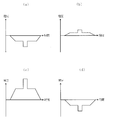
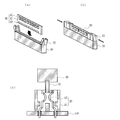
- Fig. 61 (a) is a perspective view showing a state before inserting
- Fig. 61 (b) is a perspective view showing a state after inserting.
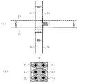
- 61C is an enlarged sectional view, and when the memory module 80 is inserted into the DIMM connector 90 fixed to the circuit board 100, connection terminals provided on the memory module 80 in the spring member 92 provided in the housing 91 are shown. 83 is pinched and electrically contacted.
- the limitations of spring-loaded mechanical structures include the problem that the entire network fails if there is a short circuit failure.
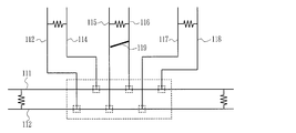
- FIG. 62 is an explanatory diagram of a short circuit fault, assuming that three pairs of wires ((113, 114), (115, 116), (117, 118)) are connected to the buses 111 and 112, respectively.
- a short circuit 119 occurs in the wires 115 and 116 of the above, the other two wires ((113, 114), (117, 118)) are also shorted via the buses 111 and 112, and a network via the buses 111 and 112 There is a problem that the whole will fail.
- the flexible substrate may be forced to be bent rapidly, and a slot (insertion port) is required, which makes it difficult to miniaturize and reduce the height.
- the present invention aims to eliminate the problems associated with the mechanical contact method and the wire exposure structure in the connector.
- a first electric wire provided with a cylindrical inner conductor coated with an insulator, and an inner conductor coated with the insulator And the connection portion of the first electric wire and the connection portion of the second electric wire are disposed close to each other, and the first electric wire and the second electric wire are connected by electromagnetic field coupling. Data connection between the two.
- the data connection is performed without contacting the first wire and the second wire at the connecting portion without using the connector of the mechanical contact method. Therefore, the problems associated with the mechanical contact system and the structure of the wire exposure in the above-mentioned connector can be eliminated.
- the contactless connection prevents direct current signals from passing and short circuit faults do not spread throughout the network. 2) Because of the non-contact connection, communication failure does not occur even if the communication distance changes due to the force of acceleration. 3) Since the electric wire is coated and made waterproof, there is no occurrence of rusting due to water immersion. 4) Even if there is a bus conflict, the current flowing to the bus is a momentary pulse-like small current and does not cause a failure. Also, even if a coupler is used, it is only provided on the first wire side, and the second wire is a general coated wire without a coupler, 5) A connection can be provided at an arbitrary place, so connection to a nearby LAN cable can be made with short wiring.
- the present invention is characterized in that, in the above (1), the second electric wire is wound around the first electric wire a plurality of times in the joint portion. As described above, by winding the second electric wire around the first electric wire a plurality of times, it is possible to effectively increase the prospect angle ⁇ and to increase the coupling efficiency, thereby downsizing the network. Becomes easier.
- the present invention is characterized in that the first electric wire and the second electric wire are disposed in parallel in the connecting portion in the above (1).
- the operation of winding one electric wire around the other electric wire becomes unnecessary.
- the second electric wire has a bonding electrode in which the inner conductor is not covered with the insulator at the bonding portion, and the bonding electrode is the It is characterized in that the circumference of the inner conductor of the electric wire of 1 is enclosed by 90 ° or more at a perspective angle. Since the first wire and the second wire can be brought closer to each other by using the bonding electrode which is not coated with the insulator in this manner, the bonding efficiency can be enhanced.
- the present invention is characterized in that, in the above (4), the bonding electrode is in direct contact with the outer periphery so as to cover the outer periphery of the insulator covering the first electric wire.
- the bonding electrode is in direct contact with the outer periphery so as to cover the outer periphery of the insulator covering the first electric wire.
- the coupling electrode is a conductor layer provided on the inner wall of the cylindrical through hole of the coupler provided with the cylindrical through hole through which the first electric wire is inserted. It is characterized by being composed of Thus, using a coupler with a coupling electrode facilitates the coupling operation and stabilizes the coupling structure.
- the coupling electrode of the second electric wire is matched and terminated. In this way, matching termination can prevent signal reflection, thereby enabling high-speed communication.
- the coupling electrode of the second electric wire is open-ended.
- the open termination eliminates the need for connection of the termination resistor, thus enabling cost reduction.
- the first electric wire has the same structure as the first electric wire which forms a differential pair with the first electric wire.
- the second electric wire has a fourth electric wire of the same structure as the second electric wire forming a differential pair with the second electric wire, and the third electric wire and the third electric wire A fourth electric wire is electromagnetically coupled at a second coupling portion located parallel to the coupling portion.
- the present invention is characterized in that in (9), the coupling electrode of the second electric wire and the coupling electrode of the fourth electric wire are matched and terminated. As described above, by matching and terminating the coupling electrode of the second electric wire and the coupling electrode of the fourth electric wire, high-speed communication can be performed because signal reflection does not occur.
- the coupling electrode of the second electric wire and the coupling electrode of the fourth electric wire are aligned and terminated on the same side in the arrangement direction in which they are arranged in parallel. It is characterized by Thus, by performing matching termination on the same side, it is possible to configure a directional coupler that propagates a signal only to the near end coupling side.
- the coupling electrode of the second electric wire and the coupling electrode of the fourth electric wire are aligned and terminated on opposite sides of the arrangement direction in which they are arranged in parallel. It is characterized by Thus, by terminating on opposite sides, the signal can be propagated left and right with the same amplitude and the same polarity.
- a conductor connecting one end of the pair of coupling electrodes is formed as a termination resistance for the matching termination.
- a transceiver is connected to each end of the pair of coupling electrodes, and the transceiver connected to the downstream side in the propagation direction is provided It is characterized in that the terminating resistor is the termination resistor. In this way, by connecting two transceivers and using the resistance provided in the transceiver as a termination resistor, it is not necessary to take time and effort to connect a termination resistor.
- the present invention is characterized in that, in the above (9), the coupling electrode of the second electric wire and the coupling electrode of the fourth electric wire are open-ended. As described above, the open termination of the coupling electrode of the second electric wire and the coupling electrode of the fourth electric wire makes the connection of the termination resistor unnecessary.
- the coupling electrode of the second electric wire and the coupling electrode of the fourth electric wire are open-ended at the same side in the arrangement direction in which they are arranged in parallel. It is characterized by In this way, by making the open termination on the same side, it is possible to propagate the half signal of the near end coupling side on the far end coupling side where the conventional signal was discarded without changing the polarity.
- the coupling electrode of the second electric wire and the coupling electrode of the fourth electric wire are open-ended on opposite sides of the arrangement direction in which they are arranged in parallel. It is characterized by thus, by open-terminating the opposite sides, the signal can be propagated with the same amplitude and the same polarity to the left and right, although the signal is slightly weakened.
- the present invention is characterized in that, in the above (9), the coupling electrode of the second electric wire and the coupling electrode of the fourth electric wire are coupled without interposing a resistance.
- the coupling electrode of the second electric wire and the coupling electrode of the fourth electric wire are coupled without interposing a resistance.
- the coupling electrode of the second electric wire and the coupling electrode of the fourth electric wire are connected on the same side in the arrangement direction in which they are arranged in parallel. It features. In this way, when connecting on the same side, the degree of coupling can be improved and the directionality can be weakened as compared with the case of matching termination on the same side.
- the coupling electrode of the second electric wire and the coupling electrode of the fourth electric wire are coupled on opposite sides of the arrangement direction in which they are arranged in parallel. It is characterized by Thus, although the signal is weakened by open-terminating the opposite sides, the signal can be propagated with the same amplitude and the same polarity from side to side.
- the first electric wire and the third electric wire are formed at positions different from the coupling portion and the second coupling portion.
- the differential pair is characterized in that the differential pair consisting of the fifth wire and the sixth wire is electromagnetically coupled.
- the first electric wire and the third electric wire are formed at positions where electromagnetic coupling can be performed with the coupling portion and the second coupling portion.
- the differential pair is characterized in that the differential pair consisting of the fifth wire and the sixth wire is electromagnetically coupled.
- the present invention in the above (22) or (23), it has transmitting means for transmitting a digital signal to a differential pair consisting of the second electric wire and the fourth electric wire, and And detecting the polarity of the pulse signal induced in the differential pair consisting of the electric wire and the third electric wire to decode the digital signal.
- transmitting means for transmitting a digital signal to a differential pair consisting of the second electric wire and the fourth electric wire, and And detecting the polarity of the pulse signal induced in the differential pair consisting of the electric wire and the third electric wire to decode the digital signal.
- transmitting means for transmitting a pulse signal of a polarity according to a digital signal to a differential pair consisting of the second electric wire and the fourth electric wire.
- a decoding means for determining the polarity of the bipolar pulse signal induced in the differential pair consisting of the first electric wire and the third electric wire to decode the digital signal.
- a pulse signal of a polarity according to the digital signal may be transmitted, and in this case, the output on the receiving side is a bipolar pulse signal. It is sufficient to determine the polarity and decode.
- the test signal is transmitted to the differential pair electromagnetically coupled to the differential pair consisting of the first electric wire and the third electric wire.
- the test signal is transmitted in advance and the received signal polarity is stored by storing the directivity. It can be returned to the polarity.
- a first electric wire provided with a cylindrical inner conductor coated with an insulator and a second electric wire provided with the inner conductor coated with an insulator.
- the electric wire is brought closer to the sum of the film thickness of the insulator covering the first electric wire in the state not to be deformed by pressing and the film thickness of the insulator covering the second electric wire in the joint portion, and electromagnetic coupling Data connection is made between a first wire and the second wire.
- bringing the two wires closer together usually allows data connection using electromagnetic coupling.
- the first electric wire has a third electric wire having the same structure as the first electric wire which forms a differential pair with the first electric wire
- the second electric wire has a fourth electric wire having the same structure as the second electric wire forming a differential pair with the second electric wire
- the third electric wire and the fourth electric wire are connected to the connection portion.
- Data connection is made between the third electric wire and the fourth electric wire by electromagnetic field coupling.
- the inner portion of a fourth electric wire of the same structure as the second electric wire formed of a conductive layer provided on the inner wall of the second cylindrical through hole and forming a differential pair with the second electric wire is characterized by having a second coupling electrode connected to the conductor.
- a coupler for differential signals can be realized by providing a pair of cylindrical through holes and coupling electrodes.
- the present invention is characterized in that, in the above (30), one end of the first coupling electrode and one end of the second coupling electrode are terminated by a termination resistance.
- the termination resistance is the same as the first coupling electrode and the first coupling electrode on the same side in the extending direction of the first coupling electrode and the second coupling electrode. It is characterized in that it is connected to the two coupled electrodes. Such a configuration makes it possible to construct a directional coupler that propagates a signal only to the near end coupling side.
- the termination resistance is the first coupling electrode and the second coupling electrode on the opposite sides in the extending direction of the first coupling electrode and the second coupling electrode. It is characterized in that it is connected to the second coupling electrode.
- the first coupling electrode is disposed on one side in the extending direction of the first cylindrical through hole in the first cylindrical through hole. It is characterized in that it is provided, and the second combined electrode is provided on the side of the second cylindrical through hole away from the first combined electrode.
- one end of the first coupling electrode and one end of the second coupling electrode are connected by a good conductor.
- the first coupling electrode and the second coupling electrode can be connected without resistance, whereby the coupling efficiency can be improved.
- the good conductor is the same as the first coupling electrode on the same side in the extending direction of the first coupling electrode and the second coupling electrode. It is characterized in that it is connected to the second coupling electrode. Such a configuration makes it possible to weaken the directivity and propagate the signal to the far end coupling side.
- the good conductor is the first coupling electrode on the opposite side of the extending direction of the first coupling electrode and the second coupling electrode. It is characterized in that it is connected to the second coupling electrode.
- the first coupling electrode is disposed on one side in the extending direction of the first cylindrical through hole in the first cylindrical through hole. It is characterized in that it is provided, and the second combined electrode is provided on the side of the second cylindrical through hole away from the first combined electrode.
- the present invention is characterized in that, in the above (30), one end of the first coupling electrode and the one end of the second coupling electrode are open-ended.
- one end of the first coupling electrode and the one end of the second coupling electrode are open-ended.
- connection point of the inner conductor of the first coupling electrode and the second electric wire, and an inner conductor of the second coupling electrode and the fourth electric wire is located on the same side of the extending direction of the first coupling electrode and the second coupling electrode.
- connection point of the inner conductor of the first coupling electrode and the second electric wire, and the inner conductor of the second coupling electrode and the fourth electric wire are opposite to each other with respect to the extending direction of the first coupling electrode and the second coupling electrode.
- the problems associated with the mechanical contact system in the connector and the structure of the electric wire exposure are eliminated using the electromagnetic field coupling system. Becomes possible.
- formula information communication network of Example 11 of this invention It is explanatory drawing (1) of a concrete operation
- FIG. 1 is an explanatory view of a coupled portion in a coated electric wire coupling type information communication network and an electromagnetic field coupling communication method according to an embodiment of the present invention
- FIG. 1 (a) is a perspective view
- FIG. It is a figure
- FIG.1 (c) is a symbol figure.
- the insulator 3 1 first the wire 1 1 having a coated central conductor 2 1, the insulator 3 2 first with the coated center conductor 2 2 of the wire 1 2 And are arranged close to each other in the joint portion 4.
- the signal propagating through one of the wires is connected to the other by conducting the signal to the other wire which is electromagnetically coupled in the coupling portion 4 to make data connection.
- the central conductors 2 1 and 2 2 in this case may be anything as long as they are good conductors, but typically Cu is used.
- As the insulator 3 1, 3 2, may be used polyethylene, it may also be further protected coated with vinyl and the like.
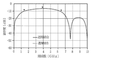
- FIG. 2 is an explanatory view of the frequency dependency of the coupling degree in the electromagnetic field coupling communication method using the coated electric wire, in which the length of the coupling portion is 20 mm and the distance between the outer peripheral surfaces of the central conductors is 2.
- the simulation was performed at 5 mm.
- the degree of coupling was -12 dB in the vicinity of 3 GHz, and it was found that a signal with an intensity of 1/4 of the signal propagating in one of the wires propagates to the second wire by electromagnetic field coupling.
- the data connection can be made by using the electromagnetic field coupling also in the case of the coated electric wire, with the result that the propagation of the signal of 1 ⁇ 4 strength is possible. It is the finding that it is possible.
- flat characteristics are shown in a relatively wide band of 1 GHz to 6 GHz, wide electromagnetic field coupling of a frequency band becomes possible.
- the center conductor 1 1, 1 degree of coupling and the distance between the second outer peripheral surface to less than 2.5mm is high, whereby the communication quality becomes high because reliability is improved, and pressed by the tape or caulking member It is desirable to shorten the distance.
- the coupling degree is reduced, but even if the interval changes within the coupling degree required for communication, communication can be performed without any problem.
- the insulating portion of one of the electric wires may be peeled off and used as a bare electric wire to form a joint electrode.
- This joint electrode may be flat, or may be cylindrical with a part of the circumference missing. It is preferable that the coupling electrode surround the inner conductor of the other wire by 90 ° or more at a perspective angle.
- FIG. 3 is an explanatory view in the case of being applied to the differential communication system
- FIG. 3 (a) is a conceptual cross-sectional view in the case of general proximity arrangement
- the first wire 1 1 and the differential signal flows to the third electrical wires 1 3 of the differential pair
- the second wire 1 2 differential signal to the fourth wire 1 4 differential pair flows the first wire 1 1 and the second wire 1 2 is electromagnetically coupled
- third electrical wires 1 3 fourth wire 1 4 are electromagnetically coupled.
- symbol 5 in a figure is a coating insulation film.
- Figure 4 is an explanatory view of the application of the differential communication system using a coupler, a differential pair of first wire 1 1 and third electrical wires 1 3, second wire 1 2 and the The differential pairs of the four electric wires 14 are electromagnetically coupled using the coupler 10.
- FIG. 5 is an explanatory view of the coupler
- FIG. 5 (a) is a conceptual perspective view of the coupler
- FIG. 5 (b) is a cross-sectional view thereof.
- the coupler 10 is formed with a bottom plate member 11 in which a pair of semi-cylindrical grooves 12 1 , 12 2 are formed, and semi-cylindrical grooves 14 1 , 14 2 in which coupling electrodes 15 1 , 15 2 are provided on the surface.
- the upper cover member 13 In order to avoid exposure of the coupling electrodes 15 1, 15 2, coupling electrodes 15 1, 15 may be coated with a second surface with a thin insulating film.
- the base plate member 11 and the upper lid member 13 may be overlapped and coupled with a screw or the like without forming the hinges 17.
- an insulator sheet is interposed between the base plate member 11 and the upper lid member 13. by pinching, it is possible to arbitrarily set the degree of coupling this insulator in a thickness of the sheet by adjusting the distance d between the wire 1 1, 1 3 and the coupling electrodes 15 1, 15 2.
- the second electric wire 1 2 (center conductor 2 2 ) and the fourth electric wire 1 4 (center conductor 2 4 ) are connected to one end of each of the coupling electrodes 15 1 and 15 2 .
- the other ends of the coupling electrodes 15 1 and 15 2 may be matched and terminated by termination resistors, may be open terminations, or may be coupled without resistance.
- the side on which the second wire 1 second and fourth wire 1 4 are connected may be at the end of the coupling electrodes 15 1, 15 2 of the same side, or to connect to the opposite ends You may
- a resistance film of 100 ⁇ may be formed in advance on one end of the flat surface between the semi-cylindrical grooves 14 1 and 14 2 .
- the coupling electrodes 15 1, 15 connect the transceiver for transmission to the second input, coupled electrodes 15 1, 15 may be connected to transceiver for terminating the second output side, transceiver for termination Can be used as the termination resistor.
- a good electric conductor film may be provided in advance at one end of the flat surface between the semi-cylindrical grooves 14 1 and 14 2 of the upper lid member 13.
- a good conductor having the same characteristic impedance as the conductor of the joint.
- FIG.5 (c) and FIG.5 (d) are sectional drawings of the modification which changed the position of the joint electrode.
- FIG. 5 (c) is a side portions housing 19 1, 19 2 of the center housing 18 is provided, the central housing 18 coupling electrode 15 to the inner surface of the groove formed in the side 3, 15 4 are provided .
- Cylindrical through holes 16 3 and 16 4 are formed by rotating the side casings 19 1 and 19 2 about the hinge 17.
- the central housing 18 and the side housings 19 1 and 19 2 are fixed by using a clip or an engagement mechanism.
- the side casings 19 1 and 19 2 on both sides of the central casing 18 are provided, and the coupling electrode is provided on the inner surface of the groove provided on the side casing 19 1 and 19 2 side.
- 15 5 and 15 6 are provided.
- Cylindrical through holes 16 5 and 16 6 are formed by rotating the side casings 19 1 and 19 2 about the hinge 17. Also in this case, the central housing 18 and the side housings 19 1 and 19 2 are fixed by using a clip and an engagement mechanism.
- the first wire 1 1 and the third wire 1 3 of the differential pair as a bus may be coupled electromagnetically at the junction of the coupling section or different positions in the same position a plurality of differential pairs. With this configuration, the same data can be broadcast to a plurality of differential pairs.
- the following operation and effect can be obtained in data communication using the coated electric wire.
- no DC signal flows and short circuit faults do not spread throughout the network.
- communication failure does not occur even if the communication distance changes due to the force of acceleration.
- the second wire is a general coated wire without a coupler
- a connection can be provided at an arbitrary place, so connection to a nearby LAN cable can be made with short wiring.
- the second electric wire can be closely arranged from the top of the insulation coating without breaking the insulation coating of the first electric wire that will be the bus main line, data can be connected easily, so installation is easy and reliability and durability are secured. It will be possible.
- the coupler is provided on both sides of the first signal line and the second signal line and coated with the same insulator as the signal line, and the signal line and the coupler are parallel plates, and the characteristic impedance is It is prescribed. Also, the communication distance is about 1 mm.
- the coupler is provided on only one side and is not coated with the same insulator as the conductor, and the conductor has a cylindrical shape and the coupler has a simple structure in the shape surrounding the same. As a result, additional connections can be easily made at any place.
- the characteristic distance is not specified (except for the example of terminating the coupler), and the communication distance is 2.5 mm to 7.5 mm as described later, because the film surrounding the cylindrical central conductor is thick. It is applicable and significant improvement in communication distance was obtained.
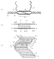
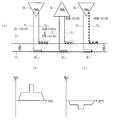
- FIG. 6 is an explanatory view of a connecting portion of the coated electric wire coupling type information communication network of Example 1 of the present invention
- FIG. 6 (a) is a sectional view in a normal state
- FIG. It is sectional drawing at the time of shortening the distance between center conductors by using.
- the coated electric wires 21 1 and 21 2 are brought close to each other to form a coupling portion, and by electromagnetic coupling at the coupling portion, data connection can be made contactlessly without using a connector requiring mechanical contact. It will be possible to do.
- the use of the tape 25 and the clasp 26 makes it possible to bring the two closer to each other to increase the degree of coupling.
- FIG. 7 is a side view of a coupling portion of the covered wire bond-type information communication network of the second embodiment of the present invention, after the center conductor 22 1 was coated with a polyethylene insulator 23 1, further vinyl protective coating 24 the covered wire 21 1 coated with 1, central conductor 22 2 then coated with polyethylene insulator 23 2, coupling section 27 a covered wire 21 2 is further coated with a vinyl protective film 24 2 by winding a plurality of times
- FIG. 8 is an explanatory view of a connection portion of a coated wire coupled information communication network according to a third embodiment of the present invention
- FIG. 8 (a) is a conceptual side view
- FIGS. 8 (b) to 8 (d) are some sectional drawings which show a contact state.
- the coupling portion 27 of the coupling line length L connected to the covered wire 21 2 of the center conductor 22 2 coupling electrode 28, the center conductor 22 of the coupling electrode 28 and the covered wire 21 1 1 and electromagnetic field coupling.
- Coupling electrode 28, FIG. 8 may be the coupling electrode 28 1 of the flat (b), the 8 cylindrical coupling, with parts cut away, of the circumference, as shown in (c) electrode 28 2 But it is good.
- coated electric wires of the differential method as shown in FIG. 8 (d), as the one covered wire 21 3 covers approximately half the circumference in the coupling electrode 28 3 to bind to the coated electric wire 21 1, while covered wire 21 4 may be the cover about half the circumference in the coupling electrode 28 4 bound to the coated electric wire 21 2.
- the longer the coupling line length L the narrower the band but the higher the degree of coupling at low frequencies, so it is suitable for low-speed communication such as for automobiles.
- the shorter the coupling line length L the weaker the degree of coupling at low frequencies, but the wider the band, which is suitable for high-speed communication.
- FIG. 9 is an explanatory view of a simulation result, and in this case, with regard to the type of coupled electrode shown in FIG. 8C, the case where the prospect angle ⁇ is 90 °, 180 °, and 270 ° is shown.
- the degree of coupling is higher as the view angle ⁇ is larger, but there is not much difference, so it is sufficient if it is about 90 °.
- FIG. 10 is an explanatory view of a connection portion of a coated wire information communication network according to a fourth embodiment of the present invention, in which a coupler is used.
- FIG. 10 (a) is an explanatory view of a coupler
- FIG. 10 (b) is an explanatory view of a coupled state.
- the coupler 30 has a bottom plate member 31 having a semi-cylindrical groove 32 formed thereon, and an upper lid member having a semi-cylindrical groove 34 having a coupling electrode 35 formed on the surface. And 33.
- FIG. 10 (b) by superimposing by rotating the bottom plate member 31 and the upper cover member 33 by a hinge 37 to the shaft, covered wire 21 1 a cylindrical through-hole 36 for inserting is formed. Further, the coupling electrode 35 center conductor 22 2 of covered wires 21 2 are connected.
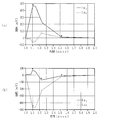
- Figure 11 is an explanatory view of the coupling degree, and the distance d between the center conductor 21 1 and the coupling electrode 35 and 2.5 mm, shows a case where the coupling line length L was 20 mm, the degree of coupling at 3GHz near was -2.584 dB.
- the degree of coupling in Example 1 is also shown for comparison, but it can be seen that the degree of coupling is significantly improved.
- FIG. 12 is an explanatory view of the dependency of the degree of coupling on the distance d.
- the perspective angle ⁇ is 180 °
- the coupling line length L is 20 mm
- the distance d is 2.5 mm, 5 mm, 7.5 mm It shows.
- FIG. 13 is an explanatory view of the coupling line length L dependency of the coupling degree.
- the prospecting angle ⁇ 180 °
- the distance d is 2.5 mm
- the coupling line length L is 20 mm, 40 mm, 60 mm Is shown.
- the degree of coupling is substantially the same, the longer the coupling line length L, the narrower the band but the higher the degree of coupling at low frequencies.
- the coupler it is possible to easily realize electromagnetic field coupling with a predetermined visual angle ⁇ , the distance d and the coupling line length L fixed.
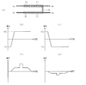
- FIG. 14 is an explanatory view of a connecting portion of the differential type coated electric wire coupling type information communication network of Example 5 of the present invention
- FIG. 14 (a) is a conceptual block diagram
- FIG. 14 (b) and FIG. 14 (c) is an explanatory view of a signal propagation state using a symbol diagram. As shown in FIG.
- the differential equation in the case of applying an electromagnetic coupling method in the covered wires are intertwined and covered wire 21 1 and covered wires 21 3 and the coupling part in the parallel state a part of the An electromagnetic field coupling is performed between the other differential type coated wires 21 2 and 21 4 .
- the output end sides of the covered electric wires 21 2 and 21 4 are matched and terminated by the 100 ⁇ termination resistor 29.
- FIG. 14 (c) is obtained by reversing the input side and the terminal side from FIG. 14 (b), and the signal propagates only in the right direction of the covered electric wires 21 1 and 21 3 forming a differential pair.
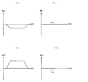
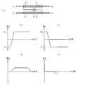
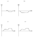
- FIGS. 15 and 16 are explanatory diagrams of the specific operation principle. First, as shown in FIG. 15A, the case where the matching termination is performed at the right end of the coupling portion will be described.
- FIG. 15 (b) is a waveform diagram showing an example of a positive signal propagating through the covered wires 21 2
- FIG. 15 (c) is a waveform diagram showing an example of a negative signal propagating covered electric wire 21 4.
- FIG. 17 is an explanatory view of a connecting portion of the coated cable type information communication network of the differential system of the fifth embodiment in the case of using a coupler
- FIG. 17 (a) is a conceptual block diagram
- b) is a perspective view of the coupler
- FIG. 17 (c) is a symbol diagram of the coupler
- FIG. 17 (d) is a cross-sectional view of the coupler.
- performing the electromagnetic field coupling with the coupler 40 1 is provided in the coupling portion.
- the coupler 40 1 is a bottom plate member 41 1 a groove 42 1 of the pair of semi-cylindrical, 42 2 are formed, coupling electrode 45 1, 45 2 are provided on the surface and a lid member 43 1 groove 44 1 of the semi-cylindrical, 44 2 are formed. Further, the flat surface of the upper cover member 43 first terminating resistor 46 for connecting the coupling electrode 45 1, 45 2 are formed.
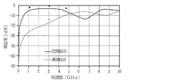
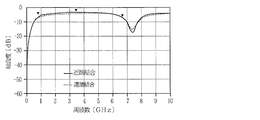
- FIG. 18 is an explanatory diagram of a frequency characteristic of a coupler used in a fifth embodiment of the present invention, in which the degree of coupling of signals by near end coupling propagating leftward becomes about ⁇ 10 dB, and far end propagating rightward The degree of signal coupling by coupling is about -20 dB, and strong directivity can be obtained.
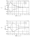
- FIG. 19 is an explanatory diagram of operation waveforms of a coupler used in a fifth embodiment of the present invention, and shows an electromagnetic field simulation result in the case of applying a step signal with an amplitude of 1 V with a rise time of 100 psec after 1 nsec.
- FIG. 19 (a) only the amplitude of 1p 1 and 1n 1 that propagates to the left of the coupler 40 1 polarity is inverted, substantially half the amplitude of the pulse signal of the step signal input Is known to propagate.
- the amplitude at a point indicated by a black inverted triangle in the figure is 0.467 V@1.111 nsec, 16.24 mV@1.520 nsec from the left side.
- the amplitude of 1p 2 and 1n 2 propagating to the right of the coupler 40 1 is very small, it can be seen that substantially no signal is propagated.
- the amplitude at the point indicated by the black inverted triangle in the figure is 70.44 mV@1.100 nsec, -65.05 mV@1.236 nsec, -9.731 mV@1.520 nsec from the left side.
- FIG. 20 is an explanatory diagram of an example of a transmitter-receiver used for a coated wire coupled information communication network according to a fifth embodiment of the present invention, having the same configuration as the transmitter-receiver used for a communication device of electromagnetic field coupling type proposed conventionally.
- Fig. 1 shows a transceiver, the transceiver of such circuitry being suitable for high speed communication.
- FIG. 21 is an explanatory view of another example of the transmitter-receiver used in the coated wire coupled information communication network according to the fifth embodiment of the present invention, and is lower than the transmitter-receiver shown in FIG. Power consumption can be achieved.
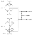
- FIG. 22 is a symbol diagram of the coupling portion of the coated electric wire coupling type information communication network of Example 6 of the present invention, in the coupling portion 27, the transmitter / receiver 381 is connected to one end of the covered electric wires 21 2 and 21 4 it is obtained by connecting the transceiver 38 2 at the other end.
- the resistance provided in the transmission / reception circuits which are disabled can be used as a termination resistance, as in the fifth embodiment.
- Which transmission / reception circuit is to be used for termination may be achieved by switching off the current source of the transmission / reception circuit on the output end side according to the signal transmission direction. For example, case of propagating signals to the left in FIG. (1p 1 and 1n 1 direction), and transmits the data in transceiver 38 1 may be a transceiver 38 2 to disable.
- FIG. 23 is an explanatory view of a connecting portion of a differential type covered wire coupling type information communication network of Example 7 of the present invention
- FIG. 23 (a) is a conceptual block diagram
- FIG. 23 (b) is a symbol It is explanatory drawing of the propagation state of the signal which used the figure.
- FIG. 23C is a perspective view of the coupler. As shown in FIG.
- Example 7 of the present invention the coupler 40 2, in the case of matching termination the end of the covered electric wire 21 2, 21 4, a pair of coupling of the coupler 40 2
- the positive electrode and the negative electrode of the electrode are disposed opposite to each other, and the matching resistor is terminated by the termination resistor 46.
- Propagation state of signal in this case the signal propagating through the covered wire 21 1 is the same as Example 5 above, signals propagating through the covered wires 21 3 propagates in the opposite direction as in Example 5 above. That is, as shown in FIG. 23 (b), 1/2 of the ideal positive signal input from the covered wire 21 2 propagates to the left in figure covered wire 21 1 by electromagnetic coupling, the other 1 / 2 is propagated through the covered electric wire 21 2 to the right, the signal propagated to the right is consumed as heat in the termination resistor 46. Therefore, when propagating a covered wire 21 1 propagates in 1p 1 direction, it does not propagate in the 1p 2 directions. Negative signal input from the covered electric wire 21 4 even with the polarity is reversed, the propagation direction is reversed.
- the calculation is performed assuming that the near end coupling is 0.5 and the far end coupling is 0.
- FIG. 23 (c) is a perspective view of a coupler coupler 40 2 is the bottom plate member 41 2 grooves 42 of the pair of semi-cylindrical 1, 42 2 are formed, coupling electrodes 45 1 to the surface, 45 2 It grooves 44 1 provided semicylindrical, 44 2 and a lid member 43 2 formed. Further, the flat surface of the upper cover member 43 second termination resistor 46 and the connection wiring 60 for connecting the coupling electrode 45 1, 45 2 are formed. In this case, in order to reduce the electromagnetic interference between the coupling electrodes 45 1, 45 2 and the connection wiring 60, it is necessary to take sufficient distance between the coupling electrodes 45 1, 45 2 and the connection wiring 60. Therefore, wider than combiner 40 1 shown in FIG. 17 (b).
- FIGS. 24 and 25 are diagrams for explaining the specific operation principle, and the signal waveform propagating in the 1p 1 direction shown in FIG. 24D and the signal waveform propagating in the 1p 2 direction shown in FIG. The same as in the case of Example 5.
- the signal waveform propagating in the 1n 1 direction shown in FIG. 25A and the signal waveform propagating in the 1n 2 direction shown in FIG. 25B have the same polarity as in Example 5, but the propagation direction is reversed. doing.
- the differential signal as shown in FIG. 25 (c) at the left end, the waveform obtained by superposing the waveform shown in FIG. 24 (d) with the waveform obtained by inverting the waveform shown in FIG. Do.
- a waveform in which the waveform obtained by inverting the waveform shown in FIG. 25 (b) and the waveform shown in FIG. 24 (e) overlap is propagated.
- the coupler propagates with the same amplitude and the same polarity in the left and right.
- FIG. 26 is an explanatory diagram of a frequency characteristic of a coupler used in a seventh embodiment of the present invention, in which the curve of near-end coupling and the curve of far-end coupling overlap and propagate with the same amplitude and the same polarity to the left and right It was confirmed to do.
- the degree of coupling at the point indicated by the black inverted triangle in the figure is from the left side: -10.126 dB@1.410 GHz, -7.255 dB@3.910 GHz, -10.604 dB@6.410 GHz.
- FIG. 27 is an explanatory diagram of an operation waveform of a coupler used in a seventh embodiment of the present invention, and also shows an electromagnetic field simulation result in the case of applying a step signal with an amplitude of 1 V with a rise time of 100 psec after 1 nsec.
- a step signal with an amplitude of 1 V with a rise time of 100 psec after 1 nsec.
- FIG. 27 (a) although 1p 1 propagating to the left of the coupler 40 2 is substantially the same as in Example 5, substantially the same as 1n 2 shows the amplitude of 1n 1 in FIG. 19 (b) become.
- the amplitude at the point indicated by the black inverted triangle in the figure is 0.4667 V@1.111 nsec, 16.24 mV@1.520 nsec from the left side.
- the amplitude at the point indicated by the white inverted triangle is -70.38 mV@1.100 nsec, 65.09 mV@1.236 nsec, 16.24 mV@1.520 nsec from the left side.
- the amplitude of 1p 2 and 1n 2 propagating to the right of the coupler 40 2 is a signal waveform obtained by inverting the 1p 1 and 1n 1 in FIG. 27 (a).
- the amplitude at the point indicated by the black inverted triangle in the figure is 70.44 mV@1.100 nsec, -65.05 mV@1.236 nsec, -9.731 mV@1.520 nsec from the left side.
- the amplitude at a point indicated by a white inverted triangle is ⁇ 469.3 mV@1.100 nsec.
- FIG. 28 is an explanatory view of a connecting portion of a modified example of the covered wire connection type information communication network of the differential type according to the seventh embodiment of the present invention
- FIG. 28 (a) is a conceptual block diagram; ) Is an explanatory view of a signal propagation state using a symbol diagram.
- FIG.28 (c) is a perspective view of a coupler.
- the coupler 40 3 and the positive electrode and the negative electrode of the pair of coupling electrodes of coupler 40 3 placed opposite to each other the terminating resistor 46 when aligning terminating end of the covered electric wire 21 2, 21 4, and eliminates the need for connecting wires the length of the coupler 40 3 long to. Therefore, the width of coupler 40 3 are the same as the width of the coupler 40 1 of Example 7. Also, as shown in FIG. 28 (b), the signal propagation state in this case is the same as that of the seventh embodiment shown in FIG. 23 (b).
- FIG. 28 (c) is a perspective view of a coupler combiner 40 3 bottom plate member 41 3 a groove 42 of a pair of semi-cylindrical 1, 42 2 are formed, coupling electrodes 45 1 to the surface, 45 2 It grooves 44 1 provided semicylindrical, 44 2 and a lid member 43 3 formed.
- one of the coupling electrodes 45 1 provided on the left half of the groove 44 1, and the other coupling electrode 45 2 is provided in the right half of the groove 44 2, directly connected to each other at the terminating resistor 46. Therefore, the step of providing the connection wiring 60 is not necessary, and the electromagnetic interference between the coupling electrodes 45 1 and 45 2 and the connection wiring 60 does not have to be taken into consideration.
- FIG. 29 is an explanatory view of a joint portion of a differential type coated wire coupling type information communication network according to an eighth embodiment of the present invention
- FIG. 29 (a) is a conceptual block diagram
- FIG. 29 (b) is a symbol
- FIG. 29 (c) is an explanatory view of a signal propagation state using a diagram
- FIG. 29 (c) is a perspective view of the coupler when the coupler is used.
- the differential equation in the case of applying an electromagnetic coupling method in the covered wires are intertwined and covered wire 21 1 and covered wires 21 3 and coupler in the parallel state a part of the 40 4 is formed, performing electromagnetic coupling between where the covered wire 21 2, 21 4 other differential equation.
- the output end sides of the covered electric wires 21 2 and 21 4 are opened to be open ends.
- a groove 42 1, 42 2 are bottom plate member 41 4 formed coupler 40 4 of the pair of semi-cylindrical in this case, the coupling electrodes 45 1 to the surface, 45 2 It grooves 44 1 provided semicylindrical, 44 2 and a lid member 43 (4) formed. In this case, no termination resistor is formed. Cylindrical penetration for inserting the covered wire 21 1, 21 3 by this case the bottom plate member 41 4 and the upper cover member 43 4 and the hinge 47 is rotated in the axis superimposed is formed.
- FIG. 30 and 31 are explanatory diagrams of a specific operation principle
- FIG. 30 (a) is a symbol diagram of a coupler, and here, a case where the right end is open-terminated will be described.
- Figure 30 (b) is a waveform diagram showing an example of a positive signal propagating through the covered wires 21 2
- FIG. 30 (c) is a waveform diagram showing an example of a negative signal propagating covered electric wire 21 4.
- An electromagnetic field coupling wave of the waveform shown appears. At the right end, the electromagnetic field coupling wave shown in FIG. 30 (e) appears.
- FIG. 32 is an explanatory diagram of the frequency characteristic of the coupler used in the eighth embodiment of the present invention, and the directivity is weaker than in the case of the matched termination shown in FIG.
- the degree of coupling at the point indicated by the black inverted triangle in the figure is from the left side: ⁇ 4.500 dB@1.160 GHz, ⁇ 1.981 dB@3.860 GHz, ⁇ 4.888 dB@4.960 GHz.
- the degree of coupling at the point indicated by the white inverted triangle is ⁇ 7.555 dB@1.160 GHz, ⁇ 4.453 dB@2.710 GHz, ⁇ 7.707 dB@5.010 GHZ from the left side.
- FIG. 33 is an explanatory diagram of the operation waveform of the coupler used in the eighth embodiment of the present invention, and also shows an electromagnetic field simulation result in the case of applying a step signal with an amplitude of 1 V with a rise time of 100 psec after 1 nsec.
- a step signal with an amplitude of 1 V with a rise time of 100 psec after 1 nsec there is.
- FIG. 33 (a) only the polarity substantially similar 1p 1 and 1n 1 propagates to the left of the coupler 40 4
- Example 5 is inverted, the step signal that is input substantially 1/2
- a pulse signal with an amplitude of Incidentally, the amplitude at a point indicated by a black inverted triangle in the figure is 0.4693 V@1.110 nsec, 9.619 mV@1.520 nsec from the left side.
- the amplitude of 1p 2 and 1n 2 propagating to the right of the coupler 40 4 about half of the amplitude signal of the signal propagating in the 1p 1 and 1n 1 direction is propagated .
- the amplitude at a point indicated by a black inverted triangle in the figure is 227.4 mV@1.520 nsec, 25.67 mV@2.370 nsec from the left side.
- the coupler since the coupler is open-ended, the signal is not discarded by the termination resistance at the far-end coupling, and the strength is effective although it is half the strength of the near-end coupling. It becomes possible to use.
- FIG. 34 is an explanatory view of a joint portion of a differential type coated wire coupling type information communication network of Example 9 of the present invention
- FIG. 34 (a) is a conceptual configuration view
- FIG. 34 (b) is a symbol It is explanatory drawing of the propagation state of the signal which used the figure.
- FIG. 34 (c) is a perspective view of the coupler. As shown in FIG.
- the coupler 40 5 in the case of open-end end portion of the covered wire 21 2, 21 4, a pair of coupling of the coupler 40 5
- the positive electrode and the negative electrode of the electrode are disposed opposite to each other and connected to the coated wires 21 2 and 21 4 .
- Negative signal input from the covered wire 21 4 signal whose polarity is reversed since the input direction is reversed is propagated in opposite directions.
- calculation is performed assuming that the near-end coupling is 0.5 and the far-end coupling is 0.
- FIG. 34 (c) is a perspective view of a coupler combiner 40 5 bottom plate member 41 5 grooves 42 1 of a pair of semi-cylindrical, 42 2 are formed, coupling electrode 45 to the surface 1, 45 2 grooves 44 1 semicylindrical provided, 44 2 and a lid member 43 5 formed.
- this Example 9 connected by opposite ends respectively coupled electrodes 45 1, 45 2 to each other with respect to coupler 40 5 center conductor 22 2, 22 4.
- 35 and 36 are diagrams for explaining the specific operation principle, and the signal waveform propagating in the 1p 1 direction shown in FIG. 35 (d) and the signal waveform propagating in the 1p 2 direction shown in FIG. 35 (e) are implemented. The same as in Example 8.
- the signal waveform propagating in the 1n 1 direction shown in FIG. 36A and the signal waveform propagating in the 1n 2 direction shown in FIG. 36B have the same polarity as in Example 8, but the propagation direction is reversed. doing.
- the differential signal as shown in FIG. 36 (c) at the left end, the waveform obtained by superposing the waveform shown in FIG. 35 (d) with the waveform obtained by inverting the waveform shown in FIG. Do.
- a waveform in which the waveform obtained by inverting the waveform shown in FIG. 36 (b) and the waveform shown in FIG. 35 (e) overlap is propagated.
- the coupler propagates with the same amplitude and the same polarity on the left and right.
- FIG. 37 is an explanatory diagram of a frequency characteristic of a coupler used in a ninth embodiment of the present invention, in which the curve of near-end coupling and the curve of far-end coupling overlap and propagate with the same amplitude on the left and right and the same polarity. It was confirmed to do.
- the degree of coupling at the point indicated by the black inverted triangle in the figure is from the left side: ⁇ 13.520 dB@0.410 GHz, ⁇ 10.450 dB@0.860 GHz, ⁇ 1.543 dB@1.260 GHz.
- FIG. 38 is an explanatory diagram of an operation waveform of a coupler used in a ninth embodiment of the present invention, and also shows an electromagnetic field simulation result in the case of applying a step signal with an amplitude of 1 V with a rise time of 100 psec after 1 nsec.
- 1p 1 propagating to the left of the coupler 40 5 is substantially the same as in Example 8, almost the same as 1n 2 shows the amplitude of 1n 1 in FIG. 33 (b) become.
- the amplitude at a point indicated by a black inverted triangle in the figure is 0.4595 V@1.142 nsec.
- the amplitude at the point indicated by the white inverted triangle is 52.66 mV@1.236 nsec, -227.4 mV@1.520 nsec from the left side.
- the amplitude of 1p 2 and 1n 2 propagating to the right of the coupler 40 2 is a signal waveform obtained by inverting the 1p 1 and 1n 1 in FIG. 38 (a).
- FIG. 39 is an explanatory view of a connection portion of a differential type coated wire coupling type information communication network of Example 10 of the present invention
- FIG. 39 (a) is a conceptual configuration view
- FIG. 39 (b) is a symbol
- FIG. 39 (c) is an explanatory view of a propagation state of a signal using a diagram
- FIG. 39 (c) is a perspective view of the coupler when the coupler is used.
- the differential equation in the case of applying an electromagnetic coupling method in the covered wires are intertwined and covered wire 21 1 and covered wires 21 3 and coupler in the parallel state a part of the 40 6 is formed, performing electromagnetic coupling between where the covered wire 21 2, 21 4 other differential equation. At this time, the output end sides of the covered electric wires 21 2 and 21 4 are connected.
- 1p 1 direction when ideally 1/2 of the normal signal propagating in the right direction by entering from the covered electric wire 21 2 propagating the covered wire 21 1 at the junction ( It propagates in the left direction and does not propagate in the 1p 2 direction (rightward direction).
- 1/2 signals connecting portion 49 to the left 1/2 1/4 of the signal of 1/2 1n 2 direction of the covered wires 21 3 It propagates and does not propagate to the 1n 1 side.
- Negative signal input from the covered electric wire 21 4 also only polarity is reversed, a similar propagation and a positive signal.
- FIG. 40 and 41 are explanatory diagrams of a specific operation principle
- FIG. 40 (a) is a symbol diagram of a coupler, and here, the case where the right ends are connected will be described.
- FIG.40 (b) is a wave form diagram which shows an example of a positive signal
- FIG.40 (c) is a wave form diagram which shows an example of a negative signal. Inductively-coupled current and capacitive coupling current when a positive signal from the covered wire 21 2 propagates toward the right end from the left end of the coupling portion flows induced in the covered wire 21 1.
- a negative signal is also capacitively coupled currents inductively coupled currents it propagates toward the left end from the right end of the covered electric wire 21 2 after exceeding the connecting portion from the covered wire 21 4 is induced in the covered wire 21 1 Flow.
- the coupling portion left covered wire 21 1 the electromagnetic field coupling wave of the waveform shown in FIG. 40 (d) appears. Also, at the right end, the electromagnetic field coupling wave shown in FIG. 40 (e) appears.
- FIG. 42 is an explanatory diagram of the frequency characteristic of the coupler used in the tenth embodiment of the present invention, and it was confirmed that the bandwidth is broadened and the directivity is weakened as compared to the matched terminal.
- the degree of coupling at the point indicated by the black inverted triangle in the figure is -7.477 dB@0.810 GHz, -3.437 dB@3.410 GHz, -7.297 dB@6.660 GHz from the left side.
- FIG. 43 is an explanatory diagram of an operation waveform of a coupler used in a tenth embodiment of the present invention, and also shows an electromagnetic field simulation result in the case of applying a step signal with an amplitude of 1 V with a rise time of 100 psec after 1 nsec.
- a As shown in FIG. 43 (a), only the amplitude of 1p 1 and 1n 1 that propagates to the left of the coupler 40 6 polarity is reversed, approximately 1/2 of the amplitude of the pulse signal of the step signal input Is known to propagate.
- the amplitude at a point indicated by a black inverted triangle in the figure is 0.4682 V@1.111 nsec, 31.65 mV@1.520 nsec from the left side.
- the amplitude of 1p 2 and 1n 2 propagating to the right of the coupler 40 6 is small, and the signal the polarity propagating in 1p 1 and 1n 1 direction is reversed.
- the amplitude at the point indicated by the white inverted triangle in the figure is 0.4107 V@1.236 nsec, 95.79 mV@1.520 nsec from the left side.
- FIG. 44 is an explanatory view of a connection portion of a differential type coated wire coupling type information communication network of Example 11 of the present invention
- FIG. 44 (a) is a conceptual configuration view
- FIG. 44 (b) is a symbol It is explanatory drawing of the propagation state of the signal which used the figure.
- FIG. 44 (c) is a perspective view of the coupler. As shown in FIG.
- Example 11 of the present invention the coupler 40 7, the end of the covered electric wire 21 2, 21 4 when linking with electrically good conductor, the coupler 40
- the positive electrode and the negative electrode of the pair of coupling electrodes 7 are arranged in the opposite direction to each other and are connected by the connecting portion 49.
- the propagation condition if the signal is, as shown in FIG. 44 (b), ideal half the positive signal propagating in the right direction by entering the covered wire 21 2 in the covered wire 21 1 at the junction it propagates in the 1p 1 direction (left direction) when propagating, not propagated in the 1p 2 direction (right direction).
- the remaining half of the signal propagates to the right of the covered wire 21 4 through a connecting portion 49, 1/2 of 1/4 of the signal of 1/2 1n 1 direction of the covered wires 21 3 It propagates and does not propagate to the 1 n 2 side.
- Negative signal input from the covered electric wire 21 4 also only the polarity and direction of propagation is reversed, the same propagation positive signal.
- Figure 44 (c) is a perspective view of a coupler combiner 40 7
- the bottom plate member 41 7 grooves 42 1 of a pair of semi-cylindrical, 42 2 are formed, coupling electrode 45 to the surface 1, 45 2 grooves 44 1 semicylindrical provided, 44 2 and a lid member 43 (7) formed.
- the flat surface of the upper cover member 43 7 is formed a connecting portion 49 connects the coupling electrode 45 1, 45 2 in good conductor.
- 45 and 46 are diagrams for explaining the specific operation principle, and the signal waveform propagating in the 1p 1 direction shown in FIG. 45 (d) and the signal waveform propagating in the 1p 2 direction shown in FIG. 45 (e) are implemented. The same as in Example 10.
- the signal waveform propagating in the 1n 1 direction shown in FIG. 46 (a) and the signal waveform propagating in the 1n 2 direction shown in FIG. 46 (b) have the same polarity as in Example 10 but the propagation direction is reversed. doing.
- the differential signal as shown in FIG. 46 (c) at the left end, the waveform obtained by overlapping the waveform shown in FIG. 46 (a) and the waveform shown in FIG. 45 (d) propagates Do.
- a waveform obtained by superposing the waveform shown in FIG. 46 (b) and the waveform shown in FIG. 45 (e) propagates to the right end side.
- the coupler propagates with the same amplitude and the same polarity on the left and right.
- FIG. 47 is an explanatory diagram of a frequency characteristic of a coupler used in Example 11 of the present invention, in which a curve of near-end coupling and a curve of far-end coupling overlap and propagate with the same amplitude and the same polarity to the left and right It was confirmed to do.
- the degree of coupling at the point indicated by the black inverted triangle in the figure is -6.734 dB@1.160 GHz, -3.909 dB@2.060 GHz, -6.649 dB@2.910 GHz from the left side.
- FIG. 48 is an explanatory diagram of the operation waveform of the coupler used in the eleventh embodiment of the present invention, and also shows an electromagnetic field simulation result in the case of applying a step signal with an amplitude of 1 V with a rise time of 100 psec after 1 nsec.
- a step signal with an amplitude of 1 V with a rise time of 100 psec after 1 nsec.
- the amplitude at a point indicated by a black inverted triangle in the figure is 0.4667 V@1.111 nsec, 22.81 mV@1.520 nsec from the left side.
- the amplitude at the point indicated by the white inverted triangle is -245.2 mV @ 1.520 nsec, -25.76 mV @ 2.370 nsec from the left side.
- the amplitude of 1p 2 and 1n 2 propagating to the right of the coupler 40 7 becomes a signal waveform obtained by inverting the 1p 1 and 1n 1 in FIG. 48 (a).
- FIG. 49 is an explanatory view of a connecting portion of a modified example of the covered wire connection type information communication network of the differential type according to the eleventh embodiment of the present invention
- FIG. 49 (a) is a conceptual block diagram; ) Is an explanatory view of a signal propagation state using a symbol diagram.
- FIG. 49 (c) is a perspective view of the coupler.
- the coupler 40 8 and the positive electrode and the negative electrode of the pair of coupling electrodes of coupler 40 8 placed opposite to each other The ends of the coated electric wires 21 2 and 21 4 are connected at the same position by the connecting portion 49 made of a good conductor. Further, as shown in FIG. 49 (b), the propagation state of the signal in this case is the same as that of the tenth embodiment shown in FIG. 44 (b).
- Figure 49 (c) is a perspective view of a coupler combiner 40 8 a bottom plate member 41 8 groove 42 1 of the pair of semi-cylindrical, 42 2 are formed, coupling electrode 45 to the surface 1, 45 2 grooves 44 1 semicylindrical provided, 44 2 and a lid member 43 8 formed.
- one of the coupling electrodes 45 1 provided on the left half of the groove 44 1, and the other coupling electrode 45 2 is provided in the right half of the groove 44 2, in the central portion, the connecting portion to connect them in good conductor Form 49. Therefore, it is not necessary to consider electromagnetic interference between the coupling electrodes 45 1 and 45 2 and the coupling portion 49.
- FIG. 50 is a symbol diagram of the coupling portion of the coated wire coupled information communication network of the twelfth embodiment of the present invention, in which one differential coated wire pair 21 1 and 21 3 is used as a bus to form three differential pairs ( (21 2 , 21 4 ), (21 5 , 21 6 ), (21 7 , 21 8 )) are electromagnetically coupled at different coupling points.
- FIG. 51 is an explanatory view of a connection portion of the coated wire combination type information communication network of Example 13 of the present invention
- FIG. 51 (a) is a symbol view
- FIG. 51 (b) is a conceptual sectional view in the connection portion. It is.
- two differential pairs ((21 2 , 21 4 ), (21 5 , 21 6 )) are used with one differential covered wire pair 21 1 , 21 3 as a bus. Are electromagnetically coupled at the same coupling point.
- a differential pair of three coated electric wires ((21 2 , 21 4 ), (21 1 , 21 3 ) and (21 5 , 21 6 )) may be pressure-welded using the caulking metal fitting 26.
- the same data propagating through the differential pair of the covered electric wires 21 1 and 21 3 serving as a bus are the differential pair of the covered electric wires 21 2 and 21 4 and the covered electric wire 21 5 it can be broadcast to the differential pair of 21 6.
- FIG. 52 is an explanatory view of a case where a coupler is used
- FIG. 52 (a) is a perspective view of the coupler
- FIG. 52 (b) is a conceptual sectional view showing a coupled state.
- Figure 52 (a) the grooves 42 1, 42 2 are formed the bottom plate member 41 coupler 40 9 coupling electrode 45 3 to the surface, 45 4 pair of which is provided a semi-cylindrical in this case 9, the coupling electrodes 45 1, 45 2 and a lid member 43 9 groove 44 1 of the semi-cylindrical, 44 2 is formed provided on the surface.
- coupling electrode 45 3, 45 4 of the bottom plate member 41 9 corresponds to the covered electric wire 21 2, 21 4, coupling electrode 45 1, 45 2 provided in the upper cover member 43 9 to covered wires 21 5, 21 6 It corresponds.
- the cylindrical through-holes 48 1, 48 2 which is rotated by the shaft inserting the covered wire 21 1, 21 3 by superimposing it is formed a bottom plate member 41 9 and the upper cover member 43 9 and the hinge 47 may .
- FIG. 53 is an explanatory view of a connection portion of a covered wire information communication network according to a modification of the thirteenth embodiment of the present invention
- FIG. 53 (a) is a symbol diagram
- FIG. 53 (b) is a concept of the connection portion.
- Cross-sectional view As shown in FIG. 53 (a), two differential pairs ((21 2 , 21 4 ), (21 5 , 21 6 )) are used with one differential covered wire pair 21 1 , 21 3 as a bus. Are electromagnetically coupled at the same coupling point. At this time, the layers are stacked in the stacking order of (21 1 , 21 3 ) / (21 2 , 21 4 ) / (21 5 , 21 6 ).
- a differential pair of three coated wires ((21 1 , 21 3 ), (21 2 , 21 4 ), (21 5 , 21 6 )) are stacked in the order of (21 1 , 21 3 ) / (21 2 , 21 4 ) / (21 5 , 21 6 ), and then pressure welding is performed using the caulking metal fitting 26. good.
- the same data propagating through the differential pair of the covered electric wires 21 1 and 21 3 serving as a bus are the differential pair of the covered electric wires 21 2 and 21 4 and the covered electric wire 21 5 it can be broadcast to the differential pair of 21 6.
- the signal transmitted to the differential pair of the covered electric wires 21 5 and 21 6 is weaker than the signal transmitted to the differential pair of the covered electric wires 21 2 and 21 4 .
- FIG. 54 is a symbol diagram of the coupled portion of the coated wire coupled information communication network of the fourteenth embodiment of the present invention, in which the pair of coated wires 21 1 and 21 3 is used as a bus to form two differential pairs ((21 2 , 21 4 ) and (21 5 , 21 6 )) are electromagnetically coupled by couplers 40 10 and 40 11 at different coupling points.
- transceiver 38 1 on the transmission side indicated by the symbol of the transmitter
- transceiver 38 2 on the reception side is shown by a symbol of the receiver.
- FIG. 55 is an explanatory view of transmission and reception waveform
- FIG. 55 (a) is a digital signal waveform of NRZ (non-return-to-zero) from the transceiver 38 1.
- Figure 55 (b) is an output waveform of the combiner 40 10, and is obtained by differentiating the waveform of the digital signal.
- Figure 55 (c) is the output waveform of the combiner 40 11, and is further differentiated waveform output of FIG. 55 (b).
- Figure 55 (d) shows a waveform of the received signal in the transceiver 38 2, determined in the transceiver 38 2, the polarity of the output waveform of the combiner 40 11 with hysteresis with the threshold values shown in FIG. 55 (c) And they are decoded into digital signals.
- This fifteenth embodiment also relates to a signal transmission-decoding method, which is an embodiment of the present invention. It is an improvement of the 14 transmission-decoding methods. That is, in the case of the method of the fourteenth embodiment, there is a problem that transmission is not performed when the same bit (0 or 1) continues, and the noise resistance is deteriorated. In addition, since the rhythm of data transmission is not constant, there is a problem that clock extraction becomes more difficult. In addition, a coupling
- 8-bit-10-bit coding or Manchester coding is performed and transmission is performed so that the same bit is not continuous in multiple bits.
- noise immunity is enhanced by latching data using the clock signal extracted by the clock extraction circuit.
- FIG. 56 is a conceptual circuit block diagram of the receiving side according to the fifteenth embodiment of the present invention, including an amplifier circuit 71 for amplifying a received signal, a determination circuit 72 for determining the polarity of the amplified signal, and a clock from the amplified signal.
- a clock extraction circuit 73 for extracting is provided, and both outputs are input to a latch circuit 74 to decode received data.
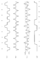
- FIG. 57 is an explanatory view of transmission and reception waveform
- FIG. 57 (a) is a digital signal waveform of NRZ (non-return-to-zero) input to the transceiver 38 1.
- FIG. 57 (b) is a Manchester encoded transmission waveform.
- Figure 57 (c) is a waveform of the transmission signal output from the transceiver 38 1. The transmission signal becomes a waveform which is differentiated by the output of the combiner 40 10, then it becomes more differentiated waveform at the output of the combiner 40 11, it is shown in FIG. 55 (b) and FIG. 55 (c)
- the same as the Figure 57 (d) is a clock waveform extracted by the clock extraction circuit in transceiver 38 2.
- FIG. 57 (e) shows a received data waveform obtained by decoding a Manchester-encoded received signal using a clock waveform.
- a coated wire information communication network according to a sixteenth embodiment of the present invention will now be described with reference to FIGS. 58 and 59.
- This sixteenth embodiment also relates to a signal transmission-decoding method, which is an embodiment of the present invention.
- This is an improvement of the transmission-decoding method of 14 or 15. That is, in the case of the method of the fourteenth or fifteenth embodiment, when the data transfer rate is low, that is, when the time to transmit the next data is long, the transmission current remains flowing. Even though the data transfer rate is slow, the transmission power becomes constant, making it difficult to reduce power consumption.
- the time during which the transmission current flows is made short and constant irrespective of the data transfer rate. Since the transmission current does not flow until the next data transfer, the transmission power can be reduced proportionately if the data transfer rate is slow.
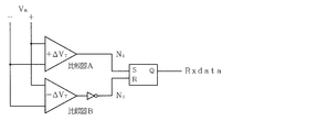
- FIG. 58 is an explanatory diagram of a receiver circuit used in a sixteenth embodiment of the present invention, in which a determination circuit is constituted by two comparison circuits.
- a short pulse is passed through the coupler of the present invention twice for transmission and reception, the signal waveform is second-order differentiated into a bipolar pulse signal as shown in FIG. 59 (c).
- a receiving circuit provided with two comparators with threshold values + ⁇ V t and ⁇ V t set.
- bonding state is the same as that of the coupling
- FIG. 59 is an explanatory view of transmission and reception waveform
- FIG. 59 (a) is a polarity of the pulse signal waveform corresponding to the digital signal from the transceiver 38 1.
- Figure 59 (b) is an output waveform of the combiner 40 10, has a pulse waveform obtained by differentiating the waveform.
- FIG. 59 (c) shows a bipolar pulse signal waveform induced in the coated electric wires 21 5 and 21 6 .
- FIG. 59 (d) compares the bipolar pulse signal waveform shown in FIG. 59 (c) with the threshold values + ⁇ V t and - ⁇ V t set in the two comparators to determine its polarity and decode the original digital signal. It is
- FIG. 60 is an explanatory diagram of a covered wire information communication network according to a seventeenth embodiment of the present invention
- FIG. 60 (a) is a symbol diagram showing a connection state
- FIGS. 60 (b) and 60 (c) are It is explanatory drawing of a received signal.
- Figure 60 (a) the use of couplers 40 12, 40 14 linked to the right of the coupling electrode coupler on the transmission side. Therefore, the differential signal waveform propagated to the left side from the differential pair consisting of the covered electric wires 21 7 and 21 8 connected on the right side becomes the waveform shown in FIG. 60 (b).
- FIG. 60 (c) the differential signal waveform propagated to the right from the differential pair consisting of the covered electric wires 21 2 and 21 4 has the strength by inverting the differential signal waveform of FIG. 60 (b) It becomes the waveform which made 1 ⁇ 2.
- the transceiver 38 1 connected to the differential pair composed of covered wires 21 2, 21 4 sends a pulse signal of 101100, since the signals propagating to the right polarity is inverted by the coupler 40 12, It becomes a pulse signal of 010011.
- the transceiver 38 2 functioning as a receiver whether the inverted signal, when receiving the inverted signal is further inverted and the inverted signal Make it return to the normal signal polarity.
- the polarity does not change unless the direction or connection order of the couplers is changed, regardless of which of the coupling ends of the couplers. Therefore, once the polarity determination is performed, data can be received correctly thereafter.
Landscapes
- Engineering & Computer Science (AREA)
- Computer Networks & Wireless Communication (AREA)
- Signal Processing (AREA)
- Near-Field Transmission Systems (AREA)
- Power Engineering (AREA)
Priority Applications (1)
| Application Number | Priority Date | Filing Date | Title |
|---|---|---|---|
| US14/891,016 US9843363B2 (en) | 2013-05-16 | 2014-05-09 | Covered wire coupling type information communication network, electromagnetic field coupling communication method and electromagnetic field coupler |
Applications Claiming Priority (2)
| Application Number | Priority Date | Filing Date | Title |
|---|---|---|---|
| JP2013-103762 | 2013-05-16 | ||
| JP2013103762A JP6181968B2 (ja) | 2013-05-16 | 2013-05-16 | 被覆電線結合式情報通信網、電磁界結合通信方法及び電磁界結合器 |
Publications (1)
| Publication Number | Publication Date |
|---|---|
| WO2014185349A1 true WO2014185349A1 (ja) | 2014-11-20 |
Family
ID=51898327
Family Applications (1)
| Application Number | Title | Priority Date | Filing Date |
|---|---|---|---|
| PCT/JP2014/062464 Ceased WO2014185349A1 (ja) | 2013-05-16 | 2014-05-09 | 被覆電線結合式情報通信網、電磁界結合通信方法及び電磁界結合器 |
Country Status (3)
| Country | Link |
|---|---|
| US (1) | US9843363B2 (https=) |
| JP (1) | JP6181968B2 (https=) |
| WO (1) | WO2014185349A1 (https=) |
Families Citing this family (5)
| Publication number | Priority date | Publication date | Assignee | Title |
|---|---|---|---|---|
| JP2015233242A (ja) * | 2014-06-10 | 2015-12-24 | パナソニックIpマネジメント株式会社 | 容量性結合器 |
| WO2016098294A1 (ja) * | 2014-12-18 | 2016-06-23 | パナソニックIpマネジメント株式会社 | 電極付き通信端末、通信端末、通信システム、電動車両、および充電装置 |
| WO2018012622A1 (ja) | 2016-07-15 | 2018-01-18 | 学校法人慶應義塾 | 回転情報伝達機器 |
| JP6991895B2 (ja) * | 2018-03-06 | 2022-01-13 | 日置電機株式会社 | Canフレーム中継装置、測定システム、記録システムおよびcanフレーム中継方法 |
| AU2020286604B2 (en) * | 2019-06-04 | 2025-11-27 | Lazzerini Societa' A Responsabilita' Limitata | Monitoring system for buses |
Citations (5)
| Publication number | Priority date | Publication date | Assignee | Title |
|---|---|---|---|---|
| US20050017908A1 (en) * | 2002-01-23 | 2005-01-27 | Atle Saegrov | Antenna device |
| JP2006038393A (ja) * | 2004-07-29 | 2006-02-09 | Mitsubishi Electric Corp | 空気調和機器、信号伝送方法および空気調和機器の信号伝送方法 |
| JP2007116464A (ja) * | 2005-10-20 | 2007-05-10 | Kansai Electric Power Co Inc:The | 電力線搬送通信装置 |
| JP2007267055A (ja) * | 2006-03-29 | 2007-10-11 | Kddi Corp | Plc信号結合装置 |
| JP2009194782A (ja) * | 2008-02-18 | 2009-08-27 | Hitachi Ltd | 電力線搬送通信装置及びその電磁結合器 |
Family Cites Families (5)
| Publication number | Priority date | Publication date | Assignee | Title |
|---|---|---|---|---|
| CN101266071B (zh) | 2004-03-09 | 2011-10-12 | 三菱电机株式会社 | 信号传输方法 |
| US7833038B1 (en) * | 2009-04-08 | 2010-11-16 | King Jr Lloyd Herbert | Inline push-in wire connectors |
| CN102498617B (zh) * | 2009-09-09 | 2015-04-01 | 株式会社村田制作所 | 天线及其制造方法、以及无线ic器件 |
| JP5638858B2 (ja) * | 2010-07-05 | 2014-12-10 | 矢崎総業株式会社 | シールド電線接続構造及びシールド電線接続方法 |
| US9419684B2 (en) | 2011-02-18 | 2016-08-16 | Keio University | Inter-module communication apparatus |
-
2013
- 2013-05-16 JP JP2013103762A patent/JP6181968B2/ja active Active
-
2014
- 2014-05-09 WO PCT/JP2014/062464 patent/WO2014185349A1/ja not_active Ceased
- 2014-05-09 US US14/891,016 patent/US9843363B2/en active Active
Patent Citations (5)
| Publication number | Priority date | Publication date | Assignee | Title |
|---|---|---|---|---|
| US20050017908A1 (en) * | 2002-01-23 | 2005-01-27 | Atle Saegrov | Antenna device |
| JP2006038393A (ja) * | 2004-07-29 | 2006-02-09 | Mitsubishi Electric Corp | 空気調和機器、信号伝送方法および空気調和機器の信号伝送方法 |
| JP2007116464A (ja) * | 2005-10-20 | 2007-05-10 | Kansai Electric Power Co Inc:The | 電力線搬送通信装置 |
| JP2007267055A (ja) * | 2006-03-29 | 2007-10-11 | Kddi Corp | Plc信号結合装置 |
| JP2009194782A (ja) * | 2008-02-18 | 2009-08-27 | Hitachi Ltd | 電力線搬送通信装置及びその電磁結合器 |
Also Published As
| Publication number | Publication date |
|---|---|
| JP2014225768A (ja) | 2014-12-04 |
| JP6181968B2 (ja) | 2017-08-16 |
| US9843363B2 (en) | 2017-12-12 |
| US20160119034A1 (en) | 2016-04-28 |
Similar Documents
| Publication | Publication Date | Title |
|---|---|---|
| CN103427143B (zh) | 波导和车内通信系统 | |
| WO2014185349A1 (ja) | 被覆電線結合式情報通信網、電磁界結合通信方法及び電磁界結合器 | |
| US7880094B2 (en) | Differential signal layout printed circuit board | |
| US8928425B1 (en) | Common mode detector for a communication system | |
| ES2541130T3 (es) | Soporte físico de conexión con compensación inductiva y capacitiva multietapa de la diafonía | |
| KR102613855B1 (ko) | 케이블 | |
| CN107112076A (zh) | 电缆 | |
| KR19980042671A (ko) | 접속 케이블과 통신 장치와 통신 방법 | |
| CN201699689U (zh) | 一种射频电路、射频测试接口装置和射频测试系统 | |
| US9716306B2 (en) | Directional coupler and communication device including same | |
| JP3033424B2 (ja) | 平衡−不平衡変換器 | |
| CN104412515A (zh) | 用于将电子元件链接到通信线的器件 | |
| CN111129681B (zh) | 一种平衡-不平衡变换装置、通信器件及通信系统 | |
| JP2008131327A (ja) | 通信線の分岐接続構造 | |
| US20160181012A1 (en) | Coupling device and coupling assembly for the contact-free transmission of data signals and method for the transmission of data signals | |
| JPH10208818A (ja) | 接続ケーブル、通信装置、および、通信方法 | |
| CN202711793U (zh) | 屏蔽线缆结构及其组合 | |
| Milosevic et al. | Optimal terminations for crosstalk mitigation of high-speed interconnects with discontinuities using modal signaling | |
| KR101320253B1 (ko) | 콘덴서 정전용량을 활용한 전력선 통신용 비접촉 커플러 및 그 제작 방법 | |
| Milosevic et al. | Crosstalk mitigation of high-speed interconnects with discontinuities using modal signaling | |
| JP2009128304A (ja) | 減結合回路 | |
| DiBiaso et al. | Designing a connection system for gigabit automotive Ethernet | |
| JP7446209B2 (ja) | 信号伝送装置 | |
| CN102369636B (zh) | 差动路径转换部件、印制基板以及电子装置 | |
| Broydé et al. | An overview of modal transmission schemes |
Legal Events
| Date | Code | Title | Description |
|---|---|---|---|
| 121 | Ep: the epo has been informed by wipo that ep was designated in this application |
Ref document number: 14798272 Country of ref document: EP Kind code of ref document: A1 |
|
| WWE | Wipo information: entry into national phase |
Ref document number: 14891016 Country of ref document: US |
|
| NENP | Non-entry into the national phase |
Ref country code: DE |
|
| 122 | Ep: pct application non-entry in european phase |
Ref document number: 14798272 Country of ref document: EP Kind code of ref document: A1 |