WO2014185349A1 - Coupled-jacketed-wire network, electromagnetic-coupling communication method, and electromagnetic coupler - Google Patents
Coupled-jacketed-wire network, electromagnetic-coupling communication method, and electromagnetic coupler Download PDFInfo
- Publication number
- WO2014185349A1 WO2014185349A1 PCT/JP2014/062464 JP2014062464W WO2014185349A1 WO 2014185349 A1 WO2014185349 A1 WO 2014185349A1 JP 2014062464 W JP2014062464 W JP 2014062464W WO 2014185349 A1 WO2014185349 A1 WO 2014185349A1
- Authority
- WO
- WIPO (PCT)
- Prior art keywords
- electric wire
- coupling
- wire
- electrode
- coupling electrode
- Prior art date
Links
- 238000010168 coupling process Methods 0.000 title claims abstract description 446
- 238000005859 coupling reaction Methods 0.000 title claims abstract description 441
- 238000004891 communication Methods 0.000 title claims abstract description 135
- 238000000034 method Methods 0.000 title claims abstract description 25
- 230000008878 coupling Effects 0.000 claims abstract description 439
- 239000004020 conductor Substances 0.000 claims description 84
- 230000005672 electromagnetic field Effects 0.000 claims description 66
- 239000012212 insulator Substances 0.000 claims description 38
- 238000012360 testing method Methods 0.000 claims description 5
- 238000003825 pressing Methods 0.000 claims description 4
- 230000008054 signal transmission Effects 0.000 claims description 3
- 230000001902 propagating effect Effects 0.000 description 56
- 238000010586 diagram Methods 0.000 description 49
- 230000005540 biological transmission Effects 0.000 description 27
- 230000000644 propagated effect Effects 0.000 description 25
- 238000004364 calculation method Methods 0.000 description 12
- 238000004088 simulation Methods 0.000 description 9
- 239000011248 coating agent Substances 0.000 description 7
- 238000000576 coating method Methods 0.000 description 7
- 230000004048 modification Effects 0.000 description 7
- 238000012986 modification Methods 0.000 description 7
- 238000000605 extraction Methods 0.000 description 6
- 238000009413 insulation Methods 0.000 description 6
- 230000007246 mechanism Effects 0.000 description 5
- 238000012546 transfer Methods 0.000 description 5
- 239000004698 Polyethylene Substances 0.000 description 4
- 230000001133 acceleration Effects 0.000 description 4
- -1 polyethylene Polymers 0.000 description 4
- 229920000573 polyethylene Polymers 0.000 description 4
- 238000004804 winding Methods 0.000 description 4
- 230000006872 improvement Effects 0.000 description 3
- 230000001939 inductive effect Effects 0.000 description 3
- 239000002184 metal Substances 0.000 description 3
- 230000009467 reduction Effects 0.000 description 3
- 239000000758 substrate Substances 0.000 description 3
- 125000000391 vinyl group Chemical group [H]C([*])=C([H])[H] 0.000 description 3
- 229920002554 vinyl polymer Polymers 0.000 description 3
- 230000008859 change Effects 0.000 description 2
- 238000007654 immersion Methods 0.000 description 2
- 238000003780 insertion Methods 0.000 description 2
- 230000037431 insertion Effects 0.000 description 2
- 238000009434 installation Methods 0.000 description 2
- 230000035515 penetration Effects 0.000 description 2
- 230000002093 peripheral effect Effects 0.000 description 2
- 230000001681 protective effect Effects 0.000 description 2
- XLYOFNOQVPJJNP-UHFFFAOYSA-N water Substances O XLYOFNOQVPJJNP-UHFFFAOYSA-N 0.000 description 2
- 229910000831 Steel Inorganic materials 0.000 description 1
- 230000009471 action Effects 0.000 description 1
- 230000003321 amplification Effects 0.000 description 1
- 230000015556 catabolic process Effects 0.000 description 1
- 230000003111 delayed effect Effects 0.000 description 1
- 230000004069 differentiation Effects 0.000 description 1
- 230000009977 dual effect Effects 0.000 description 1
- 239000000428 dust Substances 0.000 description 1
- 230000000694 effects Effects 0.000 description 1
- 230000002708 enhancing effect Effects 0.000 description 1
- 230000007613 environmental effect Effects 0.000 description 1
- 239000000446 fuel Substances 0.000 description 1
- 230000006870 function Effects 0.000 description 1
- 230000036039 immunity Effects 0.000 description 1
- 230000006698 induction Effects 0.000 description 1
- JEIPFZHSYJVQDO-UHFFFAOYSA-N iron(III) oxide Inorganic materials O=[Fe]O[Fe]=O JEIPFZHSYJVQDO-UHFFFAOYSA-N 0.000 description 1
- 238000003199 nucleic acid amplification method Methods 0.000 description 1
- 239000006223 plastic coating Substances 0.000 description 1
- 238000002360 preparation method Methods 0.000 description 1
- 239000011253 protective coating Substances 0.000 description 1
- 230000033764 rhythmic process Effects 0.000 description 1
- 238000004904 shortening Methods 0.000 description 1
- 239000010959 steel Substances 0.000 description 1
- 230000000007 visual effect Effects 0.000 description 1
- 238000003466 welding Methods 0.000 description 1
Images


Classifications
-
- H04B5/24—
-
- H—ELECTRICITY
- H04—ELECTRIC COMMUNICATION TECHNIQUE
- H04B—TRANSMISSION
- H04B3/00—Line transmission systems
- H04B3/02—Details
- H04B3/46—Monitoring; Testing
-
- H—ELECTRICITY
- H01—ELECTRIC ELEMENTS
- H01R—ELECTRICALLY-CONDUCTIVE CONNECTIONS; STRUCTURAL ASSOCIATIONS OF A PLURALITY OF MUTUALLY-INSULATED ELECTRICAL CONNECTING ELEMENTS; COUPLING DEVICES; CURRENT COLLECTORS
- H01R13/00—Details of coupling devices of the kinds covered by groups H01R12/70 or H01R24/00 - H01R33/00
- H01R13/646—Details of coupling devices of the kinds covered by groups H01R12/70 or H01R24/00 - H01R33/00 specially adapted for high-frequency, e.g. structures providing an impedance match or phase match
- H01R13/6473—Impedance matching
-
- H04B5/22—
Definitions
- the present invention relates to a coated wire coupled information communication network, an electromagnetic field coupling communication method, and an electromagnetic field coupler.
- a coated wire used in a local area network (LAN) for performing communication between modules is provided with a coupling portion
- the present invention relates to a configuration for performing high-speed data communication between modules contactlessly using capacitive coupling and inductive coupling.
- a mechanical connection method is used in which the insulation coating of the electric wire is peeled off and connected to the electrodes so that the electrodes are in contact with each other by the force of a spring.
- a communication protocol such as a control area network (Controller Area Network) with enhanced noise resistance is used.
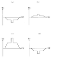
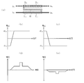
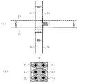
- Fig. 61 (a) is a perspective view showing a state before inserting
- Fig. 61 (b) is a perspective view showing a state after inserting.
- 61C is an enlarged sectional view, and when the memory module 80 is inserted into the DIMM connector 90 fixed to the circuit board 100, connection terminals provided on the memory module 80 in the spring member 92 provided in the housing 91 are shown. 83 is pinched and electrically contacted.
- the limitations of spring-loaded mechanical structures include the problem that the entire network fails if there is a short circuit failure.
- FIG. 62 is an explanatory diagram of a short circuit fault, assuming that three pairs of wires ((113, 114), (115, 116), (117, 118)) are connected to the buses 111 and 112, respectively.
- a short circuit 119 occurs in the wires 115 and 116 of the above, the other two wires ((113, 114), (117, 118)) are also shorted via the buses 111 and 112, and a network via the buses 111 and 112 There is a problem that the whole will fail.
- the flexible substrate may be forced to be bent rapidly, and a slot (insertion port) is required, which makes it difficult to miniaturize and reduce the height.
- the present invention aims to eliminate the problems associated with the mechanical contact method and the wire exposure structure in the connector.
- a first electric wire provided with a cylindrical inner conductor coated with an insulator, and an inner conductor coated with the insulator And the connection portion of the first electric wire and the connection portion of the second electric wire are disposed close to each other, and the first electric wire and the second electric wire are connected by electromagnetic field coupling. Data connection between the two.
- the data connection is performed without contacting the first wire and the second wire at the connecting portion without using the connector of the mechanical contact method. Therefore, the problems associated with the mechanical contact system and the structure of the wire exposure in the above-mentioned connector can be eliminated.
- the contactless connection prevents direct current signals from passing and short circuit faults do not spread throughout the network. 2) Because of the non-contact connection, communication failure does not occur even if the communication distance changes due to the force of acceleration. 3) Since the electric wire is coated and made waterproof, there is no occurrence of rusting due to water immersion. 4) Even if there is a bus conflict, the current flowing to the bus is a momentary pulse-like small current and does not cause a failure. Also, even if a coupler is used, it is only provided on the first wire side, and the second wire is a general coated wire without a coupler, 5) A connection can be provided at an arbitrary place, so connection to a nearby LAN cable can be made with short wiring.
- the present invention is characterized in that, in the above (1), the second electric wire is wound around the first electric wire a plurality of times in the joint portion. As described above, by winding the second electric wire around the first electric wire a plurality of times, it is possible to effectively increase the prospect angle ⁇ and to increase the coupling efficiency, thereby downsizing the network. Becomes easier.
- the present invention is characterized in that the first electric wire and the second electric wire are disposed in parallel in the connecting portion in the above (1).
- the operation of winding one electric wire around the other electric wire becomes unnecessary.
- the second electric wire has a bonding electrode in which the inner conductor is not covered with the insulator at the bonding portion, and the bonding electrode is the It is characterized in that the circumference of the inner conductor of the electric wire of 1 is enclosed by 90 ° or more at a perspective angle. Since the first wire and the second wire can be brought closer to each other by using the bonding electrode which is not coated with the insulator in this manner, the bonding efficiency can be enhanced.
- the present invention is characterized in that, in the above (4), the bonding electrode is in direct contact with the outer periphery so as to cover the outer periphery of the insulator covering the first electric wire.
- the bonding electrode is in direct contact with the outer periphery so as to cover the outer periphery of the insulator covering the first electric wire.
- the coupling electrode is a conductor layer provided on the inner wall of the cylindrical through hole of the coupler provided with the cylindrical through hole through which the first electric wire is inserted. It is characterized by being composed of Thus, using a coupler with a coupling electrode facilitates the coupling operation and stabilizes the coupling structure.
- the coupling electrode of the second electric wire is matched and terminated. In this way, matching termination can prevent signal reflection, thereby enabling high-speed communication.
- the coupling electrode of the second electric wire is open-ended.
- the open termination eliminates the need for connection of the termination resistor, thus enabling cost reduction.
- the first electric wire has the same structure as the first electric wire which forms a differential pair with the first electric wire.
- the second electric wire has a fourth electric wire of the same structure as the second electric wire forming a differential pair with the second electric wire, and the third electric wire and the third electric wire A fourth electric wire is electromagnetically coupled at a second coupling portion located parallel to the coupling portion.
- the present invention is characterized in that in (9), the coupling electrode of the second electric wire and the coupling electrode of the fourth electric wire are matched and terminated. As described above, by matching and terminating the coupling electrode of the second electric wire and the coupling electrode of the fourth electric wire, high-speed communication can be performed because signal reflection does not occur.
- the coupling electrode of the second electric wire and the coupling electrode of the fourth electric wire are aligned and terminated on the same side in the arrangement direction in which they are arranged in parallel. It is characterized by Thus, by performing matching termination on the same side, it is possible to configure a directional coupler that propagates a signal only to the near end coupling side.
- the coupling electrode of the second electric wire and the coupling electrode of the fourth electric wire are aligned and terminated on opposite sides of the arrangement direction in which they are arranged in parallel. It is characterized by Thus, by terminating on opposite sides, the signal can be propagated left and right with the same amplitude and the same polarity.
- a conductor connecting one end of the pair of coupling electrodes is formed as a termination resistance for the matching termination.
- a transceiver is connected to each end of the pair of coupling electrodes, and the transceiver connected to the downstream side in the propagation direction is provided It is characterized in that the terminating resistor is the termination resistor. In this way, by connecting two transceivers and using the resistance provided in the transceiver as a termination resistor, it is not necessary to take time and effort to connect a termination resistor.
- the present invention is characterized in that, in the above (9), the coupling electrode of the second electric wire and the coupling electrode of the fourth electric wire are open-ended. As described above, the open termination of the coupling electrode of the second electric wire and the coupling electrode of the fourth electric wire makes the connection of the termination resistor unnecessary.
- the coupling electrode of the second electric wire and the coupling electrode of the fourth electric wire are open-ended at the same side in the arrangement direction in which they are arranged in parallel. It is characterized by In this way, by making the open termination on the same side, it is possible to propagate the half signal of the near end coupling side on the far end coupling side where the conventional signal was discarded without changing the polarity.
- the coupling electrode of the second electric wire and the coupling electrode of the fourth electric wire are open-ended on opposite sides of the arrangement direction in which they are arranged in parallel. It is characterized by thus, by open-terminating the opposite sides, the signal can be propagated with the same amplitude and the same polarity to the left and right, although the signal is slightly weakened.
- the present invention is characterized in that, in the above (9), the coupling electrode of the second electric wire and the coupling electrode of the fourth electric wire are coupled without interposing a resistance.
- the coupling electrode of the second electric wire and the coupling electrode of the fourth electric wire are coupled without interposing a resistance.
- the coupling electrode of the second electric wire and the coupling electrode of the fourth electric wire are connected on the same side in the arrangement direction in which they are arranged in parallel. It features. In this way, when connecting on the same side, the degree of coupling can be improved and the directionality can be weakened as compared with the case of matching termination on the same side.
- the coupling electrode of the second electric wire and the coupling electrode of the fourth electric wire are coupled on opposite sides of the arrangement direction in which they are arranged in parallel. It is characterized by Thus, although the signal is weakened by open-terminating the opposite sides, the signal can be propagated with the same amplitude and the same polarity from side to side.
- the first electric wire and the third electric wire are formed at positions different from the coupling portion and the second coupling portion.
- the differential pair is characterized in that the differential pair consisting of the fifth wire and the sixth wire is electromagnetically coupled.
- the first electric wire and the third electric wire are formed at positions where electromagnetic coupling can be performed with the coupling portion and the second coupling portion.
- the differential pair is characterized in that the differential pair consisting of the fifth wire and the sixth wire is electromagnetically coupled.
- the present invention in the above (22) or (23), it has transmitting means for transmitting a digital signal to a differential pair consisting of the second electric wire and the fourth electric wire, and And detecting the polarity of the pulse signal induced in the differential pair consisting of the electric wire and the third electric wire to decode the digital signal.
- transmitting means for transmitting a digital signal to a differential pair consisting of the second electric wire and the fourth electric wire, and And detecting the polarity of the pulse signal induced in the differential pair consisting of the electric wire and the third electric wire to decode the digital signal.
- transmitting means for transmitting a pulse signal of a polarity according to a digital signal to a differential pair consisting of the second electric wire and the fourth electric wire.
- a decoding means for determining the polarity of the bipolar pulse signal induced in the differential pair consisting of the first electric wire and the third electric wire to decode the digital signal.
- a pulse signal of a polarity according to the digital signal may be transmitted, and in this case, the output on the receiving side is a bipolar pulse signal. It is sufficient to determine the polarity and decode.
- the test signal is transmitted to the differential pair electromagnetically coupled to the differential pair consisting of the first electric wire and the third electric wire.
- the test signal is transmitted in advance and the received signal polarity is stored by storing the directivity. It can be returned to the polarity.
- a first electric wire provided with a cylindrical inner conductor coated with an insulator and a second electric wire provided with the inner conductor coated with an insulator.
- the electric wire is brought closer to the sum of the film thickness of the insulator covering the first electric wire in the state not to be deformed by pressing and the film thickness of the insulator covering the second electric wire in the joint portion, and electromagnetic coupling Data connection is made between a first wire and the second wire.
- bringing the two wires closer together usually allows data connection using electromagnetic coupling.
- the first electric wire has a third electric wire having the same structure as the first electric wire which forms a differential pair with the first electric wire
- the second electric wire has a fourth electric wire having the same structure as the second electric wire forming a differential pair with the second electric wire
- the third electric wire and the fourth electric wire are connected to the connection portion.
- Data connection is made between the third electric wire and the fourth electric wire by electromagnetic field coupling.
- the inner portion of a fourth electric wire of the same structure as the second electric wire formed of a conductive layer provided on the inner wall of the second cylindrical through hole and forming a differential pair with the second electric wire is characterized by having a second coupling electrode connected to the conductor.
- a coupler for differential signals can be realized by providing a pair of cylindrical through holes and coupling electrodes.
- the present invention is characterized in that, in the above (30), one end of the first coupling electrode and one end of the second coupling electrode are terminated by a termination resistance.
- the termination resistance is the same as the first coupling electrode and the first coupling electrode on the same side in the extending direction of the first coupling electrode and the second coupling electrode. It is characterized in that it is connected to the two coupled electrodes. Such a configuration makes it possible to construct a directional coupler that propagates a signal only to the near end coupling side.
- the termination resistance is the first coupling electrode and the second coupling electrode on the opposite sides in the extending direction of the first coupling electrode and the second coupling electrode. It is characterized in that it is connected to the second coupling electrode.
- the first coupling electrode is disposed on one side in the extending direction of the first cylindrical through hole in the first cylindrical through hole. It is characterized in that it is provided, and the second combined electrode is provided on the side of the second cylindrical through hole away from the first combined electrode.
- one end of the first coupling electrode and one end of the second coupling electrode are connected by a good conductor.
- the first coupling electrode and the second coupling electrode can be connected without resistance, whereby the coupling efficiency can be improved.
- the good conductor is the same as the first coupling electrode on the same side in the extending direction of the first coupling electrode and the second coupling electrode. It is characterized in that it is connected to the second coupling electrode. Such a configuration makes it possible to weaken the directivity and propagate the signal to the far end coupling side.
- the good conductor is the first coupling electrode on the opposite side of the extending direction of the first coupling electrode and the second coupling electrode. It is characterized in that it is connected to the second coupling electrode.
- the first coupling electrode is disposed on one side in the extending direction of the first cylindrical through hole in the first cylindrical through hole. It is characterized in that it is provided, and the second combined electrode is provided on the side of the second cylindrical through hole away from the first combined electrode.
- the present invention is characterized in that, in the above (30), one end of the first coupling electrode and the one end of the second coupling electrode are open-ended.
- one end of the first coupling electrode and the one end of the second coupling electrode are open-ended.
- connection point of the inner conductor of the first coupling electrode and the second electric wire, and an inner conductor of the second coupling electrode and the fourth electric wire is located on the same side of the extending direction of the first coupling electrode and the second coupling electrode.
- connection point of the inner conductor of the first coupling electrode and the second electric wire, and the inner conductor of the second coupling electrode and the fourth electric wire are opposite to each other with respect to the extending direction of the first coupling electrode and the second coupling electrode.
- the problems associated with the mechanical contact system in the connector and the structure of the electric wire exposure are eliminated using the electromagnetic field coupling system. Becomes possible.
- formula information communication network of Example 11 of this invention It is explanatory drawing (1) of a concrete operation
- FIG. 1 is an explanatory view of a coupled portion in a coated electric wire coupling type information communication network and an electromagnetic field coupling communication method according to an embodiment of the present invention
- FIG. 1 (a) is a perspective view
- FIG. It is a figure
- FIG.1 (c) is a symbol figure.
- the insulator 3 1 first the wire 1 1 having a coated central conductor 2 1, the insulator 3 2 first with the coated center conductor 2 2 of the wire 1 2 And are arranged close to each other in the joint portion 4.
- the signal propagating through one of the wires is connected to the other by conducting the signal to the other wire which is electromagnetically coupled in the coupling portion 4 to make data connection.
- the central conductors 2 1 and 2 2 in this case may be anything as long as they are good conductors, but typically Cu is used.
- As the insulator 3 1, 3 2, may be used polyethylene, it may also be further protected coated with vinyl and the like.
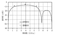
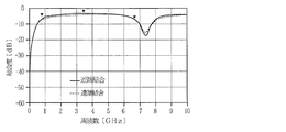
- FIG. 2 is an explanatory view of the frequency dependency of the coupling degree in the electromagnetic field coupling communication method using the coated electric wire, in which the length of the coupling portion is 20 mm and the distance between the outer peripheral surfaces of the central conductors is 2.
- the simulation was performed at 5 mm.
- the degree of coupling was -12 dB in the vicinity of 3 GHz, and it was found that a signal with an intensity of 1/4 of the signal propagating in one of the wires propagates to the second wire by electromagnetic field coupling.
- the data connection can be made by using the electromagnetic field coupling also in the case of the coated electric wire, with the result that the propagation of the signal of 1 ⁇ 4 strength is possible. It is the finding that it is possible.
- flat characteristics are shown in a relatively wide band of 1 GHz to 6 GHz, wide electromagnetic field coupling of a frequency band becomes possible.
- the center conductor 1 1, 1 degree of coupling and the distance between the second outer peripheral surface to less than 2.5mm is high, whereby the communication quality becomes high because reliability is improved, and pressed by the tape or caulking member It is desirable to shorten the distance.
- the coupling degree is reduced, but even if the interval changes within the coupling degree required for communication, communication can be performed without any problem.
- the insulating portion of one of the electric wires may be peeled off and used as a bare electric wire to form a joint electrode.
- This joint electrode may be flat, or may be cylindrical with a part of the circumference missing. It is preferable that the coupling electrode surround the inner conductor of the other wire by 90 ° or more at a perspective angle.
- FIG. 3 is an explanatory view in the case of being applied to the differential communication system
- FIG. 3 (a) is a conceptual cross-sectional view in the case of general proximity arrangement
- the first wire 1 1 and the differential signal flows to the third electrical wires 1 3 of the differential pair
- the second wire 1 2 differential signal to the fourth wire 1 4 differential pair flows the first wire 1 1 and the second wire 1 2 is electromagnetically coupled
- third electrical wires 1 3 fourth wire 1 4 are electromagnetically coupled.
- symbol 5 in a figure is a coating insulation film.
- Figure 4 is an explanatory view of the application of the differential communication system using a coupler, a differential pair of first wire 1 1 and third electrical wires 1 3, second wire 1 2 and the The differential pairs of the four electric wires 14 are electromagnetically coupled using the coupler 10.
- FIG. 5 is an explanatory view of the coupler
- FIG. 5 (a) is a conceptual perspective view of the coupler
- FIG. 5 (b) is a cross-sectional view thereof.
- the coupler 10 is formed with a bottom plate member 11 in which a pair of semi-cylindrical grooves 12 1 , 12 2 are formed, and semi-cylindrical grooves 14 1 , 14 2 in which coupling electrodes 15 1 , 15 2 are provided on the surface.
- the upper cover member 13 In order to avoid exposure of the coupling electrodes 15 1, 15 2, coupling electrodes 15 1, 15 may be coated with a second surface with a thin insulating film.
- the base plate member 11 and the upper lid member 13 may be overlapped and coupled with a screw or the like without forming the hinges 17.
- an insulator sheet is interposed between the base plate member 11 and the upper lid member 13. by pinching, it is possible to arbitrarily set the degree of coupling this insulator in a thickness of the sheet by adjusting the distance d between the wire 1 1, 1 3 and the coupling electrodes 15 1, 15 2.
- the second electric wire 1 2 (center conductor 2 2 ) and the fourth electric wire 1 4 (center conductor 2 4 ) are connected to one end of each of the coupling electrodes 15 1 and 15 2 .
- the other ends of the coupling electrodes 15 1 and 15 2 may be matched and terminated by termination resistors, may be open terminations, or may be coupled without resistance.
- the side on which the second wire 1 second and fourth wire 1 4 are connected may be at the end of the coupling electrodes 15 1, 15 2 of the same side, or to connect to the opposite ends You may
- a resistance film of 100 ⁇ may be formed in advance on one end of the flat surface between the semi-cylindrical grooves 14 1 and 14 2 .
- the coupling electrodes 15 1, 15 connect the transceiver for transmission to the second input, coupled electrodes 15 1, 15 may be connected to transceiver for terminating the second output side, transceiver for termination Can be used as the termination resistor.
- a good electric conductor film may be provided in advance at one end of the flat surface between the semi-cylindrical grooves 14 1 and 14 2 of the upper lid member 13.
- a good conductor having the same characteristic impedance as the conductor of the joint.
- FIG.5 (c) and FIG.5 (d) are sectional drawings of the modification which changed the position of the joint electrode.
- FIG. 5 (c) is a side portions housing 19 1, 19 2 of the center housing 18 is provided, the central housing 18 coupling electrode 15 to the inner surface of the groove formed in the side 3, 15 4 are provided .
- Cylindrical through holes 16 3 and 16 4 are formed by rotating the side casings 19 1 and 19 2 about the hinge 17.
- the central housing 18 and the side housings 19 1 and 19 2 are fixed by using a clip or an engagement mechanism.
- the side casings 19 1 and 19 2 on both sides of the central casing 18 are provided, and the coupling electrode is provided on the inner surface of the groove provided on the side casing 19 1 and 19 2 side.
- 15 5 and 15 6 are provided.
- Cylindrical through holes 16 5 and 16 6 are formed by rotating the side casings 19 1 and 19 2 about the hinge 17. Also in this case, the central housing 18 and the side housings 19 1 and 19 2 are fixed by using a clip and an engagement mechanism.
- the first wire 1 1 and the third wire 1 3 of the differential pair as a bus may be coupled electromagnetically at the junction of the coupling section or different positions in the same position a plurality of differential pairs. With this configuration, the same data can be broadcast to a plurality of differential pairs.
- the following operation and effect can be obtained in data communication using the coated electric wire.
- no DC signal flows and short circuit faults do not spread throughout the network.
- communication failure does not occur even if the communication distance changes due to the force of acceleration.
- the second wire is a general coated wire without a coupler
- a connection can be provided at an arbitrary place, so connection to a nearby LAN cable can be made with short wiring.
- the second electric wire can be closely arranged from the top of the insulation coating without breaking the insulation coating of the first electric wire that will be the bus main line, data can be connected easily, so installation is easy and reliability and durability are secured. It will be possible.
- the coupler is provided on both sides of the first signal line and the second signal line and coated with the same insulator as the signal line, and the signal line and the coupler are parallel plates, and the characteristic impedance is It is prescribed. Also, the communication distance is about 1 mm.
- the coupler is provided on only one side and is not coated with the same insulator as the conductor, and the conductor has a cylindrical shape and the coupler has a simple structure in the shape surrounding the same. As a result, additional connections can be easily made at any place.
- the characteristic distance is not specified (except for the example of terminating the coupler), and the communication distance is 2.5 mm to 7.5 mm as described later, because the film surrounding the cylindrical central conductor is thick. It is applicable and significant improvement in communication distance was obtained.
- FIG. 6 is an explanatory view of a connecting portion of the coated electric wire coupling type information communication network of Example 1 of the present invention
- FIG. 6 (a) is a sectional view in a normal state
- FIG. It is sectional drawing at the time of shortening the distance between center conductors by using.
- the coated electric wires 21 1 and 21 2 are brought close to each other to form a coupling portion, and by electromagnetic coupling at the coupling portion, data connection can be made contactlessly without using a connector requiring mechanical contact. It will be possible to do.
- the use of the tape 25 and the clasp 26 makes it possible to bring the two closer to each other to increase the degree of coupling.
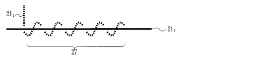
- FIG. 7 is a side view of a coupling portion of the covered wire bond-type information communication network of the second embodiment of the present invention, after the center conductor 22 1 was coated with a polyethylene insulator 23 1, further vinyl protective coating 24 the covered wire 21 1 coated with 1, central conductor 22 2 then coated with polyethylene insulator 23 2, coupling section 27 a covered wire 21 2 is further coated with a vinyl protective film 24 2 by winding a plurality of times
- FIG. 8 is an explanatory view of a connection portion of a coated wire coupled information communication network according to a third embodiment of the present invention
- FIG. 8 (a) is a conceptual side view
- FIGS. 8 (b) to 8 (d) are some sectional drawings which show a contact state.
- the coupling portion 27 of the coupling line length L connected to the covered wire 21 2 of the center conductor 22 2 coupling electrode 28, the center conductor 22 of the coupling electrode 28 and the covered wire 21 1 1 and electromagnetic field coupling.
- Coupling electrode 28, FIG. 8 may be the coupling electrode 28 1 of the flat (b), the 8 cylindrical coupling, with parts cut away, of the circumference, as shown in (c) electrode 28 2 But it is good.
- coated electric wires of the differential method as shown in FIG. 8 (d), as the one covered wire 21 3 covers approximately half the circumference in the coupling electrode 28 3 to bind to the coated electric wire 21 1, while covered wire 21 4 may be the cover about half the circumference in the coupling electrode 28 4 bound to the coated electric wire 21 2.
- the longer the coupling line length L the narrower the band but the higher the degree of coupling at low frequencies, so it is suitable for low-speed communication such as for automobiles.
- the shorter the coupling line length L the weaker the degree of coupling at low frequencies, but the wider the band, which is suitable for high-speed communication.
- FIG. 9 is an explanatory view of a simulation result, and in this case, with regard to the type of coupled electrode shown in FIG. 8C, the case where the prospect angle ⁇ is 90 °, 180 °, and 270 ° is shown.
- the degree of coupling is higher as the view angle ⁇ is larger, but there is not much difference, so it is sufficient if it is about 90 °.
- FIG. 10 is an explanatory view of a connection portion of a coated wire information communication network according to a fourth embodiment of the present invention, in which a coupler is used.
- FIG. 10 (a) is an explanatory view of a coupler
- FIG. 10 (b) is an explanatory view of a coupled state.
- the coupler 30 has a bottom plate member 31 having a semi-cylindrical groove 32 formed thereon, and an upper lid member having a semi-cylindrical groove 34 having a coupling electrode 35 formed on the surface. And 33.
- FIG. 10 (b) by superimposing by rotating the bottom plate member 31 and the upper cover member 33 by a hinge 37 to the shaft, covered wire 21 1 a cylindrical through-hole 36 for inserting is formed. Further, the coupling electrode 35 center conductor 22 2 of covered wires 21 2 are connected.
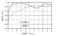
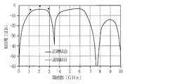
- Figure 11 is an explanatory view of the coupling degree, and the distance d between the center conductor 21 1 and the coupling electrode 35 and 2.5 mm, shows a case where the coupling line length L was 20 mm, the degree of coupling at 3GHz near was -2.584 dB.
- the degree of coupling in Example 1 is also shown for comparison, but it can be seen that the degree of coupling is significantly improved.
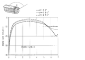
- FIG. 12 is an explanatory view of the dependency of the degree of coupling on the distance d.
- the perspective angle ⁇ is 180 °
- the coupling line length L is 20 mm
- the distance d is 2.5 mm, 5 mm, 7.5 mm It shows.
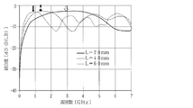
- FIG. 13 is an explanatory view of the coupling line length L dependency of the coupling degree.
- the prospecting angle ⁇ 180 °
- the distance d is 2.5 mm
- the coupling line length L is 20 mm, 40 mm, 60 mm Is shown.
- the degree of coupling is substantially the same, the longer the coupling line length L, the narrower the band but the higher the degree of coupling at low frequencies.
- the coupler it is possible to easily realize electromagnetic field coupling with a predetermined visual angle ⁇ , the distance d and the coupling line length L fixed.
- FIG. 14 is an explanatory view of a connecting portion of the differential type coated electric wire coupling type information communication network of Example 5 of the present invention
- FIG. 14 (a) is a conceptual block diagram
- FIG. 14 (b) and FIG. 14 (c) is an explanatory view of a signal propagation state using a symbol diagram. As shown in FIG.
- the differential equation in the case of applying an electromagnetic coupling method in the covered wires are intertwined and covered wire 21 1 and covered wires 21 3 and the coupling part in the parallel state a part of the An electromagnetic field coupling is performed between the other differential type coated wires 21 2 and 21 4 .
- the output end sides of the covered electric wires 21 2 and 21 4 are matched and terminated by the 100 ⁇ termination resistor 29.
- FIG. 14 (c) is obtained by reversing the input side and the terminal side from FIG. 14 (b), and the signal propagates only in the right direction of the covered electric wires 21 1 and 21 3 forming a differential pair.
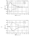
- FIGS. 15 and 16 are explanatory diagrams of the specific operation principle. First, as shown in FIG. 15A, the case where the matching termination is performed at the right end of the coupling portion will be described.
- FIG. 15 (b) is a waveform diagram showing an example of a positive signal propagating through the covered wires 21 2
- FIG. 15 (c) is a waveform diagram showing an example of a negative signal propagating covered electric wire 21 4.
- FIG. 17 is an explanatory view of a connecting portion of the coated cable type information communication network of the differential system of the fifth embodiment in the case of using a coupler
- FIG. 17 (a) is a conceptual block diagram
- b) is a perspective view of the coupler
- FIG. 17 (c) is a symbol diagram of the coupler
- FIG. 17 (d) is a cross-sectional view of the coupler.
- performing the electromagnetic field coupling with the coupler 40 1 is provided in the coupling portion.
- the coupler 40 1 is a bottom plate member 41 1 a groove 42 1 of the pair of semi-cylindrical, 42 2 are formed, coupling electrode 45 1, 45 2 are provided on the surface and a lid member 43 1 groove 44 1 of the semi-cylindrical, 44 2 are formed. Further, the flat surface of the upper cover member 43 first terminating resistor 46 for connecting the coupling electrode 45 1, 45 2 are formed.
- FIG. 18 is an explanatory diagram of a frequency characteristic of a coupler used in a fifth embodiment of the present invention, in which the degree of coupling of signals by near end coupling propagating leftward becomes about ⁇ 10 dB, and far end propagating rightward The degree of signal coupling by coupling is about -20 dB, and strong directivity can be obtained.
- FIG. 19 is an explanatory diagram of operation waveforms of a coupler used in a fifth embodiment of the present invention, and shows an electromagnetic field simulation result in the case of applying a step signal with an amplitude of 1 V with a rise time of 100 psec after 1 nsec.
- FIG. 19 (a) only the amplitude of 1p 1 and 1n 1 that propagates to the left of the coupler 40 1 polarity is inverted, substantially half the amplitude of the pulse signal of the step signal input Is known to propagate.
- the amplitude at a point indicated by a black inverted triangle in the figure is 0.467 V@1.111 nsec, 16.24 mV@1.520 nsec from the left side.
- the amplitude of 1p 2 and 1n 2 propagating to the right of the coupler 40 1 is very small, it can be seen that substantially no signal is propagated.
- the amplitude at the point indicated by the black inverted triangle in the figure is 70.44 mV@1.100 nsec, -65.05 mV@1.236 nsec, -9.731 mV@1.520 nsec from the left side.
- FIG. 20 is an explanatory diagram of an example of a transmitter-receiver used for a coated wire coupled information communication network according to a fifth embodiment of the present invention, having the same configuration as the transmitter-receiver used for a communication device of electromagnetic field coupling type proposed conventionally.
- Fig. 1 shows a transceiver, the transceiver of such circuitry being suitable for high speed communication.
- FIG. 21 is an explanatory view of another example of the transmitter-receiver used in the coated wire coupled information communication network according to the fifth embodiment of the present invention, and is lower than the transmitter-receiver shown in FIG. Power consumption can be achieved.
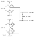
- FIG. 22 is a symbol diagram of the coupling portion of the coated electric wire coupling type information communication network of Example 6 of the present invention, in the coupling portion 27, the transmitter / receiver 381 is connected to one end of the covered electric wires 21 2 and 21 4 it is obtained by connecting the transceiver 38 2 at the other end.
- the resistance provided in the transmission / reception circuits which are disabled can be used as a termination resistance, as in the fifth embodiment.
- Which transmission / reception circuit is to be used for termination may be achieved by switching off the current source of the transmission / reception circuit on the output end side according to the signal transmission direction. For example, case of propagating signals to the left in FIG. (1p 1 and 1n 1 direction), and transmits the data in transceiver 38 1 may be a transceiver 38 2 to disable.
- FIG. 23 is an explanatory view of a connecting portion of a differential type covered wire coupling type information communication network of Example 7 of the present invention
- FIG. 23 (a) is a conceptual block diagram
- FIG. 23 (b) is a symbol It is explanatory drawing of the propagation state of the signal which used the figure.
- FIG. 23C is a perspective view of the coupler. As shown in FIG.
- Example 7 of the present invention the coupler 40 2, in the case of matching termination the end of the covered electric wire 21 2, 21 4, a pair of coupling of the coupler 40 2
- the positive electrode and the negative electrode of the electrode are disposed opposite to each other, and the matching resistor is terminated by the termination resistor 46.
- Propagation state of signal in this case the signal propagating through the covered wire 21 1 is the same as Example 5 above, signals propagating through the covered wires 21 3 propagates in the opposite direction as in Example 5 above. That is, as shown in FIG. 23 (b), 1/2 of the ideal positive signal input from the covered wire 21 2 propagates to the left in figure covered wire 21 1 by electromagnetic coupling, the other 1 / 2 is propagated through the covered electric wire 21 2 to the right, the signal propagated to the right is consumed as heat in the termination resistor 46. Therefore, when propagating a covered wire 21 1 propagates in 1p 1 direction, it does not propagate in the 1p 2 directions. Negative signal input from the covered electric wire 21 4 even with the polarity is reversed, the propagation direction is reversed.
- the calculation is performed assuming that the near end coupling is 0.5 and the far end coupling is 0.
- FIG. 23 (c) is a perspective view of a coupler coupler 40 2 is the bottom plate member 41 2 grooves 42 of the pair of semi-cylindrical 1, 42 2 are formed, coupling electrodes 45 1 to the surface, 45 2 It grooves 44 1 provided semicylindrical, 44 2 and a lid member 43 2 formed. Further, the flat surface of the upper cover member 43 second termination resistor 46 and the connection wiring 60 for connecting the coupling electrode 45 1, 45 2 are formed. In this case, in order to reduce the electromagnetic interference between the coupling electrodes 45 1, 45 2 and the connection wiring 60, it is necessary to take sufficient distance between the coupling electrodes 45 1, 45 2 and the connection wiring 60. Therefore, wider than combiner 40 1 shown in FIG. 17 (b).
- FIGS. 24 and 25 are diagrams for explaining the specific operation principle, and the signal waveform propagating in the 1p 1 direction shown in FIG. 24D and the signal waveform propagating in the 1p 2 direction shown in FIG. The same as in the case of Example 5.
- the signal waveform propagating in the 1n 1 direction shown in FIG. 25A and the signal waveform propagating in the 1n 2 direction shown in FIG. 25B have the same polarity as in Example 5, but the propagation direction is reversed. doing.
- the differential signal as shown in FIG. 25 (c) at the left end, the waveform obtained by superposing the waveform shown in FIG. 24 (d) with the waveform obtained by inverting the waveform shown in FIG. Do.
- a waveform in which the waveform obtained by inverting the waveform shown in FIG. 25 (b) and the waveform shown in FIG. 24 (e) overlap is propagated.
- the coupler propagates with the same amplitude and the same polarity in the left and right.
- FIG. 26 is an explanatory diagram of a frequency characteristic of a coupler used in a seventh embodiment of the present invention, in which the curve of near-end coupling and the curve of far-end coupling overlap and propagate with the same amplitude and the same polarity to the left and right It was confirmed to do.
- the degree of coupling at the point indicated by the black inverted triangle in the figure is from the left side: -10.126 dB@1.410 GHz, -7.255 dB@3.910 GHz, -10.604 dB@6.410 GHz.
- FIG. 27 is an explanatory diagram of an operation waveform of a coupler used in a seventh embodiment of the present invention, and also shows an electromagnetic field simulation result in the case of applying a step signal with an amplitude of 1 V with a rise time of 100 psec after 1 nsec.
- a step signal with an amplitude of 1 V with a rise time of 100 psec after 1 nsec.
- FIG. 27 (a) although 1p 1 propagating to the left of the coupler 40 2 is substantially the same as in Example 5, substantially the same as 1n 2 shows the amplitude of 1n 1 in FIG. 19 (b) become.
- the amplitude at the point indicated by the black inverted triangle in the figure is 0.4667 V@1.111 nsec, 16.24 mV@1.520 nsec from the left side.
- the amplitude at the point indicated by the white inverted triangle is -70.38 mV@1.100 nsec, 65.09 mV@1.236 nsec, 16.24 mV@1.520 nsec from the left side.
- the amplitude of 1p 2 and 1n 2 propagating to the right of the coupler 40 2 is a signal waveform obtained by inverting the 1p 1 and 1n 1 in FIG. 27 (a).
- the amplitude at the point indicated by the black inverted triangle in the figure is 70.44 mV@1.100 nsec, -65.05 mV@1.236 nsec, -9.731 mV@1.520 nsec from the left side.
- the amplitude at a point indicated by a white inverted triangle is ⁇ 469.3 mV@1.100 nsec.
- FIG. 28 is an explanatory view of a connecting portion of a modified example of the covered wire connection type information communication network of the differential type according to the seventh embodiment of the present invention
- FIG. 28 (a) is a conceptual block diagram; ) Is an explanatory view of a signal propagation state using a symbol diagram.
- FIG.28 (c) is a perspective view of a coupler.
- the coupler 40 3 and the positive electrode and the negative electrode of the pair of coupling electrodes of coupler 40 3 placed opposite to each other the terminating resistor 46 when aligning terminating end of the covered electric wire 21 2, 21 4, and eliminates the need for connecting wires the length of the coupler 40 3 long to. Therefore, the width of coupler 40 3 are the same as the width of the coupler 40 1 of Example 7. Also, as shown in FIG. 28 (b), the signal propagation state in this case is the same as that of the seventh embodiment shown in FIG. 23 (b).
- FIG. 28 (c) is a perspective view of a coupler combiner 40 3 bottom plate member 41 3 a groove 42 of a pair of semi-cylindrical 1, 42 2 are formed, coupling electrodes 45 1 to the surface, 45 2 It grooves 44 1 provided semicylindrical, 44 2 and a lid member 43 3 formed.
- one of the coupling electrodes 45 1 provided on the left half of the groove 44 1, and the other coupling electrode 45 2 is provided in the right half of the groove 44 2, directly connected to each other at the terminating resistor 46. Therefore, the step of providing the connection wiring 60 is not necessary, and the electromagnetic interference between the coupling electrodes 45 1 and 45 2 and the connection wiring 60 does not have to be taken into consideration.
- FIG. 29 is an explanatory view of a joint portion of a differential type coated wire coupling type information communication network according to an eighth embodiment of the present invention
- FIG. 29 (a) is a conceptual block diagram
- FIG. 29 (b) is a symbol
- FIG. 29 (c) is an explanatory view of a signal propagation state using a diagram
- FIG. 29 (c) is a perspective view of the coupler when the coupler is used.
- the differential equation in the case of applying an electromagnetic coupling method in the covered wires are intertwined and covered wire 21 1 and covered wires 21 3 and coupler in the parallel state a part of the 40 4 is formed, performing electromagnetic coupling between where the covered wire 21 2, 21 4 other differential equation.
- the output end sides of the covered electric wires 21 2 and 21 4 are opened to be open ends.
- a groove 42 1, 42 2 are bottom plate member 41 4 formed coupler 40 4 of the pair of semi-cylindrical in this case, the coupling electrodes 45 1 to the surface, 45 2 It grooves 44 1 provided semicylindrical, 44 2 and a lid member 43 (4) formed. In this case, no termination resistor is formed. Cylindrical penetration for inserting the covered wire 21 1, 21 3 by this case the bottom plate member 41 4 and the upper cover member 43 4 and the hinge 47 is rotated in the axis superimposed is formed.
- FIG. 30 and 31 are explanatory diagrams of a specific operation principle
- FIG. 30 (a) is a symbol diagram of a coupler, and here, a case where the right end is open-terminated will be described.
- Figure 30 (b) is a waveform diagram showing an example of a positive signal propagating through the covered wires 21 2
- FIG. 30 (c) is a waveform diagram showing an example of a negative signal propagating covered electric wire 21 4.
- An electromagnetic field coupling wave of the waveform shown appears. At the right end, the electromagnetic field coupling wave shown in FIG. 30 (e) appears.
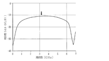
- FIG. 32 is an explanatory diagram of the frequency characteristic of the coupler used in the eighth embodiment of the present invention, and the directivity is weaker than in the case of the matched termination shown in FIG.
- the degree of coupling at the point indicated by the black inverted triangle in the figure is from the left side: ⁇ 4.500 dB@1.160 GHz, ⁇ 1.981 dB@3.860 GHz, ⁇ 4.888 dB@4.960 GHz.
- the degree of coupling at the point indicated by the white inverted triangle is ⁇ 7.555 dB@1.160 GHz, ⁇ 4.453 dB@2.710 GHz, ⁇ 7.707 dB@5.010 GHZ from the left side.
- FIG. 33 is an explanatory diagram of the operation waveform of the coupler used in the eighth embodiment of the present invention, and also shows an electromagnetic field simulation result in the case of applying a step signal with an amplitude of 1 V with a rise time of 100 psec after 1 nsec.
- a step signal with an amplitude of 1 V with a rise time of 100 psec after 1 nsec there is.
- FIG. 33 (a) only the polarity substantially similar 1p 1 and 1n 1 propagates to the left of the coupler 40 4
- Example 5 is inverted, the step signal that is input substantially 1/2
- a pulse signal with an amplitude of Incidentally, the amplitude at a point indicated by a black inverted triangle in the figure is 0.4693 V@1.110 nsec, 9.619 mV@1.520 nsec from the left side.
- the amplitude of 1p 2 and 1n 2 propagating to the right of the coupler 40 4 about half of the amplitude signal of the signal propagating in the 1p 1 and 1n 1 direction is propagated .
- the amplitude at a point indicated by a black inverted triangle in the figure is 227.4 mV@1.520 nsec, 25.67 mV@2.370 nsec from the left side.
- the coupler since the coupler is open-ended, the signal is not discarded by the termination resistance at the far-end coupling, and the strength is effective although it is half the strength of the near-end coupling. It becomes possible to use.
- FIG. 34 is an explanatory view of a joint portion of a differential type coated wire coupling type information communication network of Example 9 of the present invention
- FIG. 34 (a) is a conceptual configuration view
- FIG. 34 (b) is a symbol It is explanatory drawing of the propagation state of the signal which used the figure.
- FIG. 34 (c) is a perspective view of the coupler. As shown in FIG.
- the coupler 40 5 in the case of open-end end portion of the covered wire 21 2, 21 4, a pair of coupling of the coupler 40 5
- the positive electrode and the negative electrode of the electrode are disposed opposite to each other and connected to the coated wires 21 2 and 21 4 .
- Negative signal input from the covered wire 21 4 signal whose polarity is reversed since the input direction is reversed is propagated in opposite directions.
- calculation is performed assuming that the near-end coupling is 0.5 and the far-end coupling is 0.
- FIG. 34 (c) is a perspective view of a coupler combiner 40 5 bottom plate member 41 5 grooves 42 1 of a pair of semi-cylindrical, 42 2 are formed, coupling electrode 45 to the surface 1, 45 2 grooves 44 1 semicylindrical provided, 44 2 and a lid member 43 5 formed.
- this Example 9 connected by opposite ends respectively coupled electrodes 45 1, 45 2 to each other with respect to coupler 40 5 center conductor 22 2, 22 4.
- 35 and 36 are diagrams for explaining the specific operation principle, and the signal waveform propagating in the 1p 1 direction shown in FIG. 35 (d) and the signal waveform propagating in the 1p 2 direction shown in FIG. 35 (e) are implemented. The same as in Example 8.
- the signal waveform propagating in the 1n 1 direction shown in FIG. 36A and the signal waveform propagating in the 1n 2 direction shown in FIG. 36B have the same polarity as in Example 8, but the propagation direction is reversed. doing.
- the differential signal as shown in FIG. 36 (c) at the left end, the waveform obtained by superposing the waveform shown in FIG. 35 (d) with the waveform obtained by inverting the waveform shown in FIG. Do.
- a waveform in which the waveform obtained by inverting the waveform shown in FIG. 36 (b) and the waveform shown in FIG. 35 (e) overlap is propagated.
- the coupler propagates with the same amplitude and the same polarity on the left and right.
- FIG. 37 is an explanatory diagram of a frequency characteristic of a coupler used in a ninth embodiment of the present invention, in which the curve of near-end coupling and the curve of far-end coupling overlap and propagate with the same amplitude on the left and right and the same polarity. It was confirmed to do.
- the degree of coupling at the point indicated by the black inverted triangle in the figure is from the left side: ⁇ 13.520 dB@0.410 GHz, ⁇ 10.450 dB@0.860 GHz, ⁇ 1.543 dB@1.260 GHz.
- FIG. 38 is an explanatory diagram of an operation waveform of a coupler used in a ninth embodiment of the present invention, and also shows an electromagnetic field simulation result in the case of applying a step signal with an amplitude of 1 V with a rise time of 100 psec after 1 nsec.
- 1p 1 propagating to the left of the coupler 40 5 is substantially the same as in Example 8, almost the same as 1n 2 shows the amplitude of 1n 1 in FIG. 33 (b) become.
- the amplitude at a point indicated by a black inverted triangle in the figure is 0.4595 V@1.142 nsec.
- the amplitude at the point indicated by the white inverted triangle is 52.66 mV@1.236 nsec, -227.4 mV@1.520 nsec from the left side.
- the amplitude of 1p 2 and 1n 2 propagating to the right of the coupler 40 2 is a signal waveform obtained by inverting the 1p 1 and 1n 1 in FIG. 38 (a).
- FIG. 39 is an explanatory view of a connection portion of a differential type coated wire coupling type information communication network of Example 10 of the present invention
- FIG. 39 (a) is a conceptual configuration view
- FIG. 39 (b) is a symbol
- FIG. 39 (c) is an explanatory view of a propagation state of a signal using a diagram
- FIG. 39 (c) is a perspective view of the coupler when the coupler is used.
- the differential equation in the case of applying an electromagnetic coupling method in the covered wires are intertwined and covered wire 21 1 and covered wires 21 3 and coupler in the parallel state a part of the 40 6 is formed, performing electromagnetic coupling between where the covered wire 21 2, 21 4 other differential equation. At this time, the output end sides of the covered electric wires 21 2 and 21 4 are connected.
- 1p 1 direction when ideally 1/2 of the normal signal propagating in the right direction by entering from the covered electric wire 21 2 propagating the covered wire 21 1 at the junction ( It propagates in the left direction and does not propagate in the 1p 2 direction (rightward direction).
- 1/2 signals connecting portion 49 to the left 1/2 1/4 of the signal of 1/2 1n 2 direction of the covered wires 21 3 It propagates and does not propagate to the 1n 1 side.
- Negative signal input from the covered electric wire 21 4 also only polarity is reversed, a similar propagation and a positive signal.
- FIG. 40 and 41 are explanatory diagrams of a specific operation principle
- FIG. 40 (a) is a symbol diagram of a coupler, and here, the case where the right ends are connected will be described.
- FIG.40 (b) is a wave form diagram which shows an example of a positive signal
- FIG.40 (c) is a wave form diagram which shows an example of a negative signal. Inductively-coupled current and capacitive coupling current when a positive signal from the covered wire 21 2 propagates toward the right end from the left end of the coupling portion flows induced in the covered wire 21 1.
- a negative signal is also capacitively coupled currents inductively coupled currents it propagates toward the left end from the right end of the covered electric wire 21 2 after exceeding the connecting portion from the covered wire 21 4 is induced in the covered wire 21 1 Flow.
- the coupling portion left covered wire 21 1 the electromagnetic field coupling wave of the waveform shown in FIG. 40 (d) appears. Also, at the right end, the electromagnetic field coupling wave shown in FIG. 40 (e) appears.
- FIG. 42 is an explanatory diagram of the frequency characteristic of the coupler used in the tenth embodiment of the present invention, and it was confirmed that the bandwidth is broadened and the directivity is weakened as compared to the matched terminal.
- the degree of coupling at the point indicated by the black inverted triangle in the figure is -7.477 dB@0.810 GHz, -3.437 dB@3.410 GHz, -7.297 dB@6.660 GHz from the left side.
- FIG. 43 is an explanatory diagram of an operation waveform of a coupler used in a tenth embodiment of the present invention, and also shows an electromagnetic field simulation result in the case of applying a step signal with an amplitude of 1 V with a rise time of 100 psec after 1 nsec.
- a As shown in FIG. 43 (a), only the amplitude of 1p 1 and 1n 1 that propagates to the left of the coupler 40 6 polarity is reversed, approximately 1/2 of the amplitude of the pulse signal of the step signal input Is known to propagate.
- the amplitude at a point indicated by a black inverted triangle in the figure is 0.4682 V@1.111 nsec, 31.65 mV@1.520 nsec from the left side.
- the amplitude of 1p 2 and 1n 2 propagating to the right of the coupler 40 6 is small, and the signal the polarity propagating in 1p 1 and 1n 1 direction is reversed.
- the amplitude at the point indicated by the white inverted triangle in the figure is 0.4107 V@1.236 nsec, 95.79 mV@1.520 nsec from the left side.
- FIG. 44 is an explanatory view of a connection portion of a differential type coated wire coupling type information communication network of Example 11 of the present invention
- FIG. 44 (a) is a conceptual configuration view
- FIG. 44 (b) is a symbol It is explanatory drawing of the propagation state of the signal which used the figure.
- FIG. 44 (c) is a perspective view of the coupler. As shown in FIG.
- Example 11 of the present invention the coupler 40 7, the end of the covered electric wire 21 2, 21 4 when linking with electrically good conductor, the coupler 40
- the positive electrode and the negative electrode of the pair of coupling electrodes 7 are arranged in the opposite direction to each other and are connected by the connecting portion 49.
- the propagation condition if the signal is, as shown in FIG. 44 (b), ideal half the positive signal propagating in the right direction by entering the covered wire 21 2 in the covered wire 21 1 at the junction it propagates in the 1p 1 direction (left direction) when propagating, not propagated in the 1p 2 direction (right direction).
- the remaining half of the signal propagates to the right of the covered wire 21 4 through a connecting portion 49, 1/2 of 1/4 of the signal of 1/2 1n 1 direction of the covered wires 21 3 It propagates and does not propagate to the 1 n 2 side.
- Negative signal input from the covered electric wire 21 4 also only the polarity and direction of propagation is reversed, the same propagation positive signal.
- Figure 44 (c) is a perspective view of a coupler combiner 40 7
- the bottom plate member 41 7 grooves 42 1 of a pair of semi-cylindrical, 42 2 are formed, coupling electrode 45 to the surface 1, 45 2 grooves 44 1 semicylindrical provided, 44 2 and a lid member 43 (7) formed.
- the flat surface of the upper cover member 43 7 is formed a connecting portion 49 connects the coupling electrode 45 1, 45 2 in good conductor.
- 45 and 46 are diagrams for explaining the specific operation principle, and the signal waveform propagating in the 1p 1 direction shown in FIG. 45 (d) and the signal waveform propagating in the 1p 2 direction shown in FIG. 45 (e) are implemented. The same as in Example 10.
- the signal waveform propagating in the 1n 1 direction shown in FIG. 46 (a) and the signal waveform propagating in the 1n 2 direction shown in FIG. 46 (b) have the same polarity as in Example 10 but the propagation direction is reversed. doing.
- the differential signal as shown in FIG. 46 (c) at the left end, the waveform obtained by overlapping the waveform shown in FIG. 46 (a) and the waveform shown in FIG. 45 (d) propagates Do.
- a waveform obtained by superposing the waveform shown in FIG. 46 (b) and the waveform shown in FIG. 45 (e) propagates to the right end side.
- the coupler propagates with the same amplitude and the same polarity on the left and right.
- FIG. 47 is an explanatory diagram of a frequency characteristic of a coupler used in Example 11 of the present invention, in which a curve of near-end coupling and a curve of far-end coupling overlap and propagate with the same amplitude and the same polarity to the left and right It was confirmed to do.
- the degree of coupling at the point indicated by the black inverted triangle in the figure is -6.734 dB@1.160 GHz, -3.909 dB@2.060 GHz, -6.649 dB@2.910 GHz from the left side.
- FIG. 48 is an explanatory diagram of the operation waveform of the coupler used in the eleventh embodiment of the present invention, and also shows an electromagnetic field simulation result in the case of applying a step signal with an amplitude of 1 V with a rise time of 100 psec after 1 nsec.
- a step signal with an amplitude of 1 V with a rise time of 100 psec after 1 nsec.
- the amplitude at a point indicated by a black inverted triangle in the figure is 0.4667 V@1.111 nsec, 22.81 mV@1.520 nsec from the left side.
- the amplitude at the point indicated by the white inverted triangle is -245.2 mV @ 1.520 nsec, -25.76 mV @ 2.370 nsec from the left side.
- the amplitude of 1p 2 and 1n 2 propagating to the right of the coupler 40 7 becomes a signal waveform obtained by inverting the 1p 1 and 1n 1 in FIG. 48 (a).
- FIG. 49 is an explanatory view of a connecting portion of a modified example of the covered wire connection type information communication network of the differential type according to the eleventh embodiment of the present invention
- FIG. 49 (a) is a conceptual block diagram; ) Is an explanatory view of a signal propagation state using a symbol diagram.
- FIG. 49 (c) is a perspective view of the coupler.
- the coupler 40 8 and the positive electrode and the negative electrode of the pair of coupling electrodes of coupler 40 8 placed opposite to each other The ends of the coated electric wires 21 2 and 21 4 are connected at the same position by the connecting portion 49 made of a good conductor. Further, as shown in FIG. 49 (b), the propagation state of the signal in this case is the same as that of the tenth embodiment shown in FIG. 44 (b).
- Figure 49 (c) is a perspective view of a coupler combiner 40 8 a bottom plate member 41 8 groove 42 1 of the pair of semi-cylindrical, 42 2 are formed, coupling electrode 45 to the surface 1, 45 2 grooves 44 1 semicylindrical provided, 44 2 and a lid member 43 8 formed.
- one of the coupling electrodes 45 1 provided on the left half of the groove 44 1, and the other coupling electrode 45 2 is provided in the right half of the groove 44 2, in the central portion, the connecting portion to connect them in good conductor Form 49. Therefore, it is not necessary to consider electromagnetic interference between the coupling electrodes 45 1 and 45 2 and the coupling portion 49.
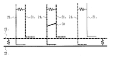
- FIG. 50 is a symbol diagram of the coupling portion of the coated wire coupled information communication network of the twelfth embodiment of the present invention, in which one differential coated wire pair 21 1 and 21 3 is used as a bus to form three differential pairs ( (21 2 , 21 4 ), (21 5 , 21 6 ), (21 7 , 21 8 )) are electromagnetically coupled at different coupling points.
- FIG. 51 is an explanatory view of a connection portion of the coated wire combination type information communication network of Example 13 of the present invention
- FIG. 51 (a) is a symbol view
- FIG. 51 (b) is a conceptual sectional view in the connection portion. It is.
- two differential pairs ((21 2 , 21 4 ), (21 5 , 21 6 )) are used with one differential covered wire pair 21 1 , 21 3 as a bus. Are electromagnetically coupled at the same coupling point.
- a differential pair of three coated electric wires ((21 2 , 21 4 ), (21 1 , 21 3 ) and (21 5 , 21 6 )) may be pressure-welded using the caulking metal fitting 26.
- the same data propagating through the differential pair of the covered electric wires 21 1 and 21 3 serving as a bus are the differential pair of the covered electric wires 21 2 and 21 4 and the covered electric wire 21 5 it can be broadcast to the differential pair of 21 6.
- FIG. 52 is an explanatory view of a case where a coupler is used
- FIG. 52 (a) is a perspective view of the coupler
- FIG. 52 (b) is a conceptual sectional view showing a coupled state.
- Figure 52 (a) the grooves 42 1, 42 2 are formed the bottom plate member 41 coupler 40 9 coupling electrode 45 3 to the surface, 45 4 pair of which is provided a semi-cylindrical in this case 9, the coupling electrodes 45 1, 45 2 and a lid member 43 9 groove 44 1 of the semi-cylindrical, 44 2 is formed provided on the surface.
- coupling electrode 45 3, 45 4 of the bottom plate member 41 9 corresponds to the covered electric wire 21 2, 21 4, coupling electrode 45 1, 45 2 provided in the upper cover member 43 9 to covered wires 21 5, 21 6 It corresponds.
- the cylindrical through-holes 48 1, 48 2 which is rotated by the shaft inserting the covered wire 21 1, 21 3 by superimposing it is formed a bottom plate member 41 9 and the upper cover member 43 9 and the hinge 47 may .
- FIG. 53 is an explanatory view of a connection portion of a covered wire information communication network according to a modification of the thirteenth embodiment of the present invention
- FIG. 53 (a) is a symbol diagram
- FIG. 53 (b) is a concept of the connection portion.
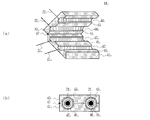
- Cross-sectional view As shown in FIG. 53 (a), two differential pairs ((21 2 , 21 4 ), (21 5 , 21 6 )) are used with one differential covered wire pair 21 1 , 21 3 as a bus. Are electromagnetically coupled at the same coupling point. At this time, the layers are stacked in the stacking order of (21 1 , 21 3 ) / (21 2 , 21 4 ) / (21 5 , 21 6 ).
- a differential pair of three coated wires ((21 1 , 21 3 ), (21 2 , 21 4 ), (21 5 , 21 6 )) are stacked in the order of (21 1 , 21 3 ) / (21 2 , 21 4 ) / (21 5 , 21 6 ), and then pressure welding is performed using the caulking metal fitting 26. good.
- the same data propagating through the differential pair of the covered electric wires 21 1 and 21 3 serving as a bus are the differential pair of the covered electric wires 21 2 and 21 4 and the covered electric wire 21 5 it can be broadcast to the differential pair of 21 6.
- the signal transmitted to the differential pair of the covered electric wires 21 5 and 21 6 is weaker than the signal transmitted to the differential pair of the covered electric wires 21 2 and 21 4 .
- FIG. 54 is a symbol diagram of the coupled portion of the coated wire coupled information communication network of the fourteenth embodiment of the present invention, in which the pair of coated wires 21 1 and 21 3 is used as a bus to form two differential pairs ((21 2 , 21 4 ) and (21 5 , 21 6 )) are electromagnetically coupled by couplers 40 10 and 40 11 at different coupling points.
- transceiver 38 1 on the transmission side indicated by the symbol of the transmitter
- transceiver 38 2 on the reception side is shown by a symbol of the receiver.
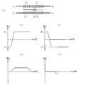
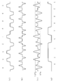
- FIG. 55 is an explanatory view of transmission and reception waveform
- FIG. 55 (a) is a digital signal waveform of NRZ (non-return-to-zero) from the transceiver 38 1.
- Figure 55 (b) is an output waveform of the combiner 40 10, and is obtained by differentiating the waveform of the digital signal.
- Figure 55 (c) is the output waveform of the combiner 40 11, and is further differentiated waveform output of FIG. 55 (b).
- Figure 55 (d) shows a waveform of the received signal in the transceiver 38 2, determined in the transceiver 38 2, the polarity of the output waveform of the combiner 40 11 with hysteresis with the threshold values shown in FIG. 55 (c) And they are decoded into digital signals.
- This fifteenth embodiment also relates to a signal transmission-decoding method, which is an embodiment of the present invention. It is an improvement of the 14 transmission-decoding methods. That is, in the case of the method of the fourteenth embodiment, there is a problem that transmission is not performed when the same bit (0 or 1) continues, and the noise resistance is deteriorated. In addition, since the rhythm of data transmission is not constant, there is a problem that clock extraction becomes more difficult. In addition, a coupling
- 8-bit-10-bit coding or Manchester coding is performed and transmission is performed so that the same bit is not continuous in multiple bits.
- noise immunity is enhanced by latching data using the clock signal extracted by the clock extraction circuit.
- FIG. 56 is a conceptual circuit block diagram of the receiving side according to the fifteenth embodiment of the present invention, including an amplifier circuit 71 for amplifying a received signal, a determination circuit 72 for determining the polarity of the amplified signal, and a clock from the amplified signal.
- a clock extraction circuit 73 for extracting is provided, and both outputs are input to a latch circuit 74 to decode received data.
- FIG. 57 is an explanatory view of transmission and reception waveform
- FIG. 57 (a) is a digital signal waveform of NRZ (non-return-to-zero) input to the transceiver 38 1.
- FIG. 57 (b) is a Manchester encoded transmission waveform.
- Figure 57 (c) is a waveform of the transmission signal output from the transceiver 38 1. The transmission signal becomes a waveform which is differentiated by the output of the combiner 40 10, then it becomes more differentiated waveform at the output of the combiner 40 11, it is shown in FIG. 55 (b) and FIG. 55 (c)
- the same as the Figure 57 (d) is a clock waveform extracted by the clock extraction circuit in transceiver 38 2.
- FIG. 57 (e) shows a received data waveform obtained by decoding a Manchester-encoded received signal using a clock waveform.
- a coated wire information communication network according to a sixteenth embodiment of the present invention will now be described with reference to FIGS. 58 and 59.
- This sixteenth embodiment also relates to a signal transmission-decoding method, which is an embodiment of the present invention.
- This is an improvement of the transmission-decoding method of 14 or 15. That is, in the case of the method of the fourteenth or fifteenth embodiment, when the data transfer rate is low, that is, when the time to transmit the next data is long, the transmission current remains flowing. Even though the data transfer rate is slow, the transmission power becomes constant, making it difficult to reduce power consumption.
- the time during which the transmission current flows is made short and constant irrespective of the data transfer rate. Since the transmission current does not flow until the next data transfer, the transmission power can be reduced proportionately if the data transfer rate is slow.
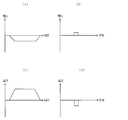
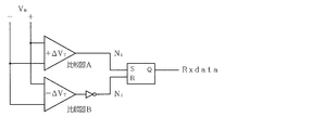
- FIG. 58 is an explanatory diagram of a receiver circuit used in a sixteenth embodiment of the present invention, in which a determination circuit is constituted by two comparison circuits.
- a short pulse is passed through the coupler of the present invention twice for transmission and reception, the signal waveform is second-order differentiated into a bipolar pulse signal as shown in FIG. 59 (c).
- a receiving circuit provided with two comparators with threshold values + ⁇ V t and ⁇ V t set.
- bonding state is the same as that of the coupling
- FIG. 59 is an explanatory view of transmission and reception waveform
- FIG. 59 (a) is a polarity of the pulse signal waveform corresponding to the digital signal from the transceiver 38 1.
- Figure 59 (b) is an output waveform of the combiner 40 10, has a pulse waveform obtained by differentiating the waveform.
- FIG. 59 (c) shows a bipolar pulse signal waveform induced in the coated electric wires 21 5 and 21 6 .
- FIG. 59 (d) compares the bipolar pulse signal waveform shown in FIG. 59 (c) with the threshold values + ⁇ V t and - ⁇ V t set in the two comparators to determine its polarity and decode the original digital signal. It is
- FIG. 60 is an explanatory diagram of a covered wire information communication network according to a seventeenth embodiment of the present invention
- FIG. 60 (a) is a symbol diagram showing a connection state
- FIGS. 60 (b) and 60 (c) are It is explanatory drawing of a received signal.
- Figure 60 (a) the use of couplers 40 12, 40 14 linked to the right of the coupling electrode coupler on the transmission side. Therefore, the differential signal waveform propagated to the left side from the differential pair consisting of the covered electric wires 21 7 and 21 8 connected on the right side becomes the waveform shown in FIG. 60 (b).
- FIG. 60 (c) the differential signal waveform propagated to the right from the differential pair consisting of the covered electric wires 21 2 and 21 4 has the strength by inverting the differential signal waveform of FIG. 60 (b) It becomes the waveform which made 1 ⁇ 2.
- the transceiver 38 1 connected to the differential pair composed of covered wires 21 2, 21 4 sends a pulse signal of 101100, since the signals propagating to the right polarity is inverted by the coupler 40 12, It becomes a pulse signal of 010011.
- the transceiver 38 2 functioning as a receiver whether the inverted signal, when receiving the inverted signal is further inverted and the inverted signal Make it return to the normal signal polarity.
- the polarity does not change unless the direction or connection order of the couplers is changed, regardless of which of the coupling ends of the couplers. Therefore, once the polarity determination is performed, data can be received correctly thereafter.
Abstract
This invention, which pertains to a coupled-jacketed-wire network, an electromagnetic-coupling communication method, and an electromagnetic coupler, solves the problems that accompany wire-exposure structures and mechanical connection schemes for connectors. A first jacketed wire and a second jacketed wire are laid out in close proximity to each other in a coupling unit, and electromagnetic coupling in said coupling unit creates a data connection between said first and second jacketed wires.
Description
本発明は、被覆電線結合式情報通信網、電磁界結合通信方法及び電磁界結合器に関するもので、例えば、モジュール間の通信を行うローカルエリアネットワーク(LAN)に用いる被覆電線同士を結合部を設けて容量結合及び誘導結合を利用して、非接触でモジュール間で高速にデータ通信する構成に関するものである。
The present invention relates to a coated wire coupled information communication network, an electromagnetic field coupling communication method, and an electromagnetic field coupler. For example, a coated wire used in a local area network (LAN) for performing communication between modules is provided with a coupling portion The present invention relates to a configuration for performing high-speed data communication between modules contactlessly using capacitive coupling and inductive coupling.
従来、モジュールを組み合わせてシステムを構築する場合、各モジュール間の信号配線はコネクタで接続されている。本発明者は、このようなコネクタに代わる電気的に非接触の信号伝達方法を提案している(例えば、特許文献1、或いは、非特許文献1乃至非特許文献3参照)。
Conventionally, when constructing a system by combining modules, signal wires between the modules are connected by connectors. The inventor of the present invention has proposed an electrical non-contact signal transmission method as an alternative to such a connector (see, for example, Patent Document 1 or Non-Patent Documents 1 to 3).
一方、従来から広く用いられているコネクタでは、電線の絶縁被覆を剥いて電極に接続し電極同士をバネの力で接触させる機械式接続方式が用いられている。また、車載用途などにおいては、通信プロトコルには、耐ノイズ性を強化したコントロール・エリア・ネットワーク(Controller Area Network)等の通信規格が用いられている。
On the other hand, in a connector which has been widely used conventionally, a mechanical connection method is used in which the insulation coating of the electric wire is peeled off and connected to the electrodes so that the electrodes are in contact with each other by the force of a spring. In addition, in an on-vehicle application and the like, a communication protocol such as a control area network (Controller Area Network) with enhanced noise resistance is used.
ここで、図61を参照して従来の機械式コネクタを用いた結合機構を説明する。図61(a)は、差し込む前の状態を示す斜視図であり、図61(b)は差し込んだ後の状態を示す斜視図である。基板81にメモリ素子82を実装したメモリモジュール80をDIMM(Dual Inline Memory Module)コネクタ90に差し込んだのち、両側に設けた留め金93でメモリモジュール80を固定する。
Here, referring to FIG. 61, a coupling mechanism using a conventional mechanical connector will be described. Fig. 61 (a) is a perspective view showing a state before inserting, and Fig. 61 (b) is a perspective view showing a state after inserting. After inserting the memory module 80 in which the memory element 82 is mounted on the substrate 81 into a dual inline memory module (DIMM) connector 90, the memory module 80 is fixed by clasps 93 provided on both sides.
図61(c)は拡大断面図であり、回路基板100に固定されたDIMMコネクタ90にメモリモジュール80を差し込むと、筐体91内に設けられたバネ部材92にメモリモジュール80に設けた接続端子83が挟撃されて電気的に接触する構成となっている。
61C is an enlarged sectional view, and when the memory module 80 is inserted into the DIMM connector 90 fixed to the circuit board 100, connection terminals provided on the memory module 80 in the spring member 92 provided in the housing 91 are shown. 83 is pinched and electrically contacted.
このような車載用途や航空機搭載用途においては高信頼性が求められるため、信頼性及び耐久性、小型化及び低背化、さらには、高速化、多極化、高密度化及び低操作力化が求められている。
Since high reliability is required for such in-vehicle applications and aircraft-mounted applications, reliability, durability, miniaturization and height reduction, speedup, multipolarization, high density and low operation force are required. It is done.
このうち、信頼性及び耐久性としては、瞬断事故に対応するための耐振性及び耐衝撃性が求められ、また、高温、高湿度、温度変化或いはゴミやホコリに対応する環境耐久性が求められる。さらに、機械的差し込みに対する挿抜耐久性や、静電破壊に対する電磁ノイズ耐久性が求められている。
Among these, as reliability and durability, vibration resistance and impact resistance are required for responding to a momentary accident, and environmental durability is required for high temperature, high humidity, temperature change or dust and dirt. Be Furthermore, the insertion-and-extraction durability with respect to mechanical insertion and the electromagnetic noise tolerance with respect to an electrostatic breakdown are calculated | required.
しかし、従来のコネクタでは、バネで接触させる機械構造からくる限界や、電線が露出している構造からくる限界等の各種の限界がある。例えば、バネで接触させる機械構造からくる限界としては、短絡故障があるとネットワーク全体が不全となるという問題が挙げられる。
However, in the conventional connector, there are various limitations such as a limitation caused by a spring-contacting mechanical structure and a limitation caused by a structure in which a wire is exposed. For example, the limitations of spring-loaded mechanical structures include the problem that the entire network fails if there is a short circuit failure.
図62は、短絡故障の説明図であり、バス111,112に3対の配線((113,114)、(115,116)、(117,118))が接続されていると仮定すると、一対の配線115,116に短絡119が発生した場合、バス111,112を介して他の2つの配線((113,114)、(117,118))も短絡し、バス111,112を介したネットワーク全体が不全になるという問題がある。
FIG. 62 is an explanatory diagram of a short circuit fault, assuming that three pairs of wires ((113, 114), (115, 116), (117, 118)) are connected to the buses 111 and 112, respectively. When a short circuit 119 occurs in the wires 115 and 116 of the above, the other two wires ((113, 114), (117, 118)) are also shorted via the buses 111 and 112, and a network via the buses 111 and 112 There is a problem that the whole will fail.
また、耐振性及び耐衝撃性に対する対策を講じていても、自動車や航空機の場合には、コネクタに大きな加速度による力が加わる場合があり、このような大きな加速度が加わった場合には瞬断不良が起こるという問題がある。
In addition, even if measures are taken against vibration resistance and impact resistance, in the case of an automobile or aircraft, a large acceleration force may be applied to the connector, and when such a large acceleration is applied, a short break occurs There is a problem that occurs.
また、上述のように、従来コネクタでは電線が露出しているため、コネクタの接点が浸水で錆付き接触不良を起こすという問題もある。また、一般に複数のコネクタが集積されたコネクタボックスが用いられるので、最短配線でLANに接続することができず配線重量が増えるという問題がある。特に、車載用途或いは航空機搭載用途では燃費を悪くする要因になる。
Further, as described above, in the conventional connector, since the electric wire is exposed, there is also a problem that the contact point of the connector is flooded to cause rust and a contact failure. In addition, since a connector box in which a plurality of connectors are integrated is generally used, it is not possible to connect to a LAN with the shortest wiring, and there is a problem that the wiring weight increases. In particular, it is a factor which worsens fuel consumption in on-vehicle use or airborne application.
また、経時使用において、新たな接続が必要になる場合に備えて、必要以上のコネクタを予め設置する必要があり、小型化や低背化を阻害する要因となる。また、2つの出力回路が同時に信号を送信(バスコンフリクト)した時、バスに過大な電流が流れ続けて故障の原因となり得るという問題もある。
In addition, it is necessary to install in advance more connectors than necessary in preparation for the need for a new connection in use over time, which is a factor that hinders miniaturization and reduction in height. In addition, when two output circuits simultaneously transmit signals (bus conflict), there is a problem that an excessive current continues to flow in the bus, which may cause a failure.
さらに、接続に際しては、フレキ基板の急激な曲げを強いる場合があるとともに、スロット(差込口)が必要になるため、小型化や低背化が困難であるという問題がある。
Further, in connection with the connection, the flexible substrate may be forced to be bent rapidly, and a slot (insertion port) is required, which makes it difficult to miniaturize and reduce the height.
また、バネによる接触であるので、インピーダンス不整合が起こって伝送する信号品質が劣化するという問題や、信号漏洩の問題がある。また、コネクタによる接続の場合には、LSIテスタの装着が困難であるという問題もある。例えば、LSIチップとLSIテスタとの接続本数が非常に多くなる場合、機械的に同時接続するために相当大きな力が必要になる。因みに、1チップあたり500本の接続があり、500チップを同時テストすることを想定すると、接続数が25万本となり、何トンという荷重がかかることになる。
In addition, because of the contact by the spring, there is a problem that impedance mismatch occurs and the signal quality to be transmitted is deteriorated, and a problem of signal leakage. Further, in the case of connection by a connector, there is also a problem that it is difficult to mount the LSI tester. For example, when the number of connections between an LSI chip and an LSI tester is extremely large, a considerable amount of force is required to mechanically connect simultaneously. Incidentally, if there are 500 connections per chip, and it is assumed that 500 chips will be tested simultaneously, the number of connections will be 250,000 and a load of several tons will be applied.
したがって、本発明は、コネクタにおける機械的接触方式及び電線露出の構造に伴う問題点を解消することを目的とする。
SUMMARY OF THE INVENTION Accordingly, the present invention aims to eliminate the problems associated with the mechanical contact method and the wire exposure structure in the connector.
(1)上記の課題を解決するために、被覆電線結合式情報通信網において、絶縁物で被覆された円筒状の内部導体を備えた第1の電線と、絶縁物で被覆された内部導体を備えた第2の電線とを有し、前記第1の電線の結合部と前記第2の電線の結合部が近接配置されて、電磁界結合により前記第1の電線と前記第2の電線との間でデータ接続を行うことを特徴とする。
(1) In order to solve the above-mentioned problems, in a covered electric wire coupling type information communication network, a first electric wire provided with a cylindrical inner conductor coated with an insulator, and an inner conductor coated with the insulator And the connection portion of the first electric wire and the connection portion of the second electric wire are disposed close to each other, and the first electric wire and the second electric wire are connected by electromagnetic field coupling. Data connection between the two.
このように、被覆電線を用いている場合にも、機械的接触方式のコネクタを用いずに、第1の電線と第2の電線を結合部で近接させて非接触でデータ接続を行っているので、上述のコネクタにおける機械的接触方式及び電線露出の構造に伴う問題点を解消することができる。
As described above, even when using the coated wire, the data connection is performed without contacting the first wire and the second wire at the connecting portion without using the connector of the mechanical contact method. Therefore, the problems associated with the mechanical contact system and the structure of the wire exposure in the above-mentioned connector can be eliminated.
即ち、
1)非接触接続なので直流信号が通過せず、短絡故障がネットワーク全体に波及しない。
2)非接触接続なので加速度による力が加わり通信距離が変化しても通信不良が起こらない。
3)電線が被膜されて防水構造になっているので、浸水による錆付きが発生することがない。
4)バスコンフリクトしても、バスに流れる電流は瞬時のパルス状の小さな電流であるので故障の原因とならない。
また、結合器を用いたとしても、第1の電線側に設けるだけであり、第2の電線は結合器のない一般の被覆電線であるので、
5)任意の箇所に結合部を設ければ良いので、近くのLANケーブルに短い配線で接続できる。
6)結合部を任意の箇所に設けるだけであるので、必要に応じて後から接続を追加できる。
7)バス基幹線となる第1の電線の絶縁被覆を破らずに絶縁被覆の上から第2の電線を近接配置してデータ接続できるので、設置が容易であり信頼性・耐久性の確保が可能になる。 That is,
1) The contactless connection prevents direct current signals from passing and short circuit faults do not spread throughout the network.
2) Because of the non-contact connection, communication failure does not occur even if the communication distance changes due to the force of acceleration.
3) Since the electric wire is coated and made waterproof, there is no occurrence of rusting due to water immersion.
4) Even if there is a bus conflict, the current flowing to the bus is a momentary pulse-like small current and does not cause a failure.
Also, even if a coupler is used, it is only provided on the first wire side, and the second wire is a general coated wire without a coupler,
5) A connection can be provided at an arbitrary place, so connection to a nearby LAN cable can be made with short wiring.
6) It is possible to add a connection later if necessary, since only the coupling portion is provided at an arbitrary position.
7) Since the second electric wire can be closely arranged from the top of the insulation coating without breaking the insulation coating of the first electric wire that will be the bus main line, data can be connected easily, so installation is easy and reliability and durability are secured. It will be possible.
(2)また、本発明は上記(1)において、前記結合部において、前記第2の電線が、前記第1の電線の周囲に複数回巻回していることを特徴とする。このように、前記第2の電線を前記第1の電線の周囲に複数回巻回させることによって、見込み角θを実効的に大きくして結合効率を大きくすることができるので、ネットワークの小型化が容易になる。
(2) Further, the present invention is characterized in that, in the above (1), the second electric wire is wound around the first electric wire a plurality of times in the joint portion. As described above, by winding the second electric wire around the first electric wire a plurality of times, it is possible to effectively increase the prospect angle θ and to increase the coupling efficiency, thereby downsizing the network. Becomes easier.
(3)また、本発明は上記(1)において、前記結合部において、前記第1の電線と前記第2の電線が平行に配置されたことを特徴とする。このように、前記第1の電線と前記第2の電線とを平行に配置することによって、一方の電線を他方の電線に巻回する作業が不要になる。
(3) Further, the present invention is characterized in that the first electric wire and the second electric wire are disposed in parallel in the connecting portion in the above (1). Thus, by arranging the first electric wire and the second electric wire in parallel, the operation of winding one electric wire around the other electric wire becomes unnecessary.
(4)また、本発明は上記(3)において、前記第2の電線は、前記結合部において、前記内部導体が前記絶縁物に被覆されていない結合電極を有し、前記結合電極は前記第1の電線の内部導体の周囲を見込み角で90°以上囲っていることを特徴とする。このように絶縁物に被覆されていない結合電極を用いることによって第1の電線と第2の電線をより近接させることができるので、結合効率を高めることができる。
(4) Further, in the present invention according to (3), the second electric wire has a bonding electrode in which the inner conductor is not covered with the insulator at the bonding portion, and the bonding electrode is the It is characterized in that the circumference of the inner conductor of the electric wire of 1 is enclosed by 90 ° or more at a perspective angle. Since the first wire and the second wire can be brought closer to each other by using the bonding electrode which is not coated with the insulator in this manner, the bonding efficiency can be enhanced.
(5)また、本発明は、上記(4)において、前記結合電極は、前記第1の電線を被覆する絶縁物の外周を覆うように、前記外周に直接接していることを特徴とする。このように、結合電極を第1の電線を被覆する絶縁物の外周を接するようにして覆うことにより、両者の距離をより近接させ、それにより、結合効率を高めることができる。
(5) Further, the present invention is characterized in that, in the above (4), the bonding electrode is in direct contact with the outer periphery so as to cover the outer periphery of the insulator covering the first electric wire. As described above, by covering the bonding electrode so as to contact the outer periphery of the insulator covering the first electric wire, it is possible to make the distance between the two closer, thereby enhancing the bonding efficiency.
(6)また、本発明は上記(4)において、前記結合電極は、前記第1の電線を挿通する円筒状貫通孔を備えた結合器の前記円筒状貫通孔の内壁に設けられた導体層により構成されることを特徴とする。このように、結合電極を備えた結合器を用いることによって結合作業が容易になるとともに、結合構造が安定になる。
(6) Further, according to the present invention, in the above (4), the coupling electrode is a conductor layer provided on the inner wall of the cylindrical through hole of the coupler provided with the cylindrical through hole through which the first electric wire is inserted. It is characterized by being composed of Thus, using a coupler with a coupling electrode facilitates the coupling operation and stabilizes the coupling structure.
(7)また、本発明は、上記(4)乃至(6)のいずれかにおいて、前記第2の電線の結合電極が整合終端していることを特徴とする。このように、整合終端させることによって、信号の反射を防止することができ、それによって、高速通信が可能になる。
(7) Further, in the present invention, in any one of the above (4) to (6), the coupling electrode of the second electric wire is matched and terminated. In this way, matching termination can prevent signal reflection, thereby enabling high-speed communication.
(8)また、本発明は、上記(4)乃至(6)のいずれかにおいて、前記第2の電線の結合電極が開放終端していることを特徴とする。このように、開放終端させることによって、終端抵抗の接続が不要になるので低コスト化が可能になる。
(8) Further, in the present invention, in any one of the above (4) to (6), the coupling electrode of the second electric wire is open-ended. As described above, the open termination eliminates the need for connection of the termination resistor, thus enabling cost reduction.
(9)また、本発明は、上記(3)乃至(6)のいずれかにおいて、前記第1の電線は該第1の電線と差動対を形成する前記第1の電線と同じ構造の第3の電線と有するとともに、前記第2の電線は該第2の電線と差動対を形成する前記第2の電線と同じ構造の第4の電線を有し、前記第3の電線と前記第4の電線が前記結合部と平行に位置する第2の結合部において電磁界結合していることを特徴とする。このような構成を用いることによって、差動信号を用いた信号通信においても、コネクタにおける機械的接触方式及び電線露出の構造に伴う問題点を解消することができる。
(9) Further, according to the present invention, in any one of the above (3) to (6), the first electric wire has the same structure as the first electric wire which forms a differential pair with the first electric wire. And the second electric wire has a fourth electric wire of the same structure as the second electric wire forming a differential pair with the second electric wire, and the third electric wire and the third electric wire A fourth electric wire is electromagnetically coupled at a second coupling portion located parallel to the coupling portion. By using such a configuration, even in the signal communication using differential signals, it is possible to solve the problems associated with the mechanical contact system in the connector and the structure of the wire exposure.
(10)また、本発明は、上記(9)において、前記第2の電線の結合電極と前記第4の電線の結合電極が整合終端していることを特徴とする。このように、前記第2の電線の結合電極と前記第4の電線の結合電極を整合終端することによって、信号の反射が起こらないので、高速通信が可能になる。
(10) Further, the present invention is characterized in that in (9), the coupling electrode of the second electric wire and the coupling electrode of the fourth electric wire are matched and terminated. As described above, by matching and terminating the coupling electrode of the second electric wire and the coupling electrode of the fourth electric wire, high-speed communication can be performed because signal reflection does not occur.
(11)また、本発明は、上記(10)において、前記第2の電線の結合電極と前記第4の電線の結合電極が、平行に配列する配列方向の同じ側で整合終端していることを特徴とする。このように、同じ側で整合終端させることによって、近端結合側にのみ信号を伝搬する方向性結合器を構成することができる。
(11) Further, according to the present invention, in the above (10), the coupling electrode of the second electric wire and the coupling electrode of the fourth electric wire are aligned and terminated on the same side in the arrangement direction in which they are arranged in parallel. It is characterized by Thus, by performing matching termination on the same side, it is possible to configure a directional coupler that propagates a signal only to the near end coupling side.
(12)また、本発明は、上記(10)において、前記第2の電線の結合電極と前記第4の電線の結合電極が、平行に配列する配列方向の互いに反対側で整合終端していることを特徴とする。このように、互いに反対側で終端させることによって、信号を左右に同じ振幅且つ同じ極性で伝搬させることができる。
(12) Further, according to the present invention, in the above (10), the coupling electrode of the second electric wire and the coupling electrode of the fourth electric wire are aligned and terminated on opposite sides of the arrangement direction in which they are arranged in parallel. It is characterized by Thus, by terminating on opposite sides, the signal can be propagated left and right with the same amplitude and the same polarity.
(13)また、本発明は、上記(10)乃至(12)において、前記第1の電線及び前記第3の電線をそれぞれ挿通する一対の平行な円筒状貫通孔と、前記一対の円筒状貫通孔の内壁に設けられた導体層からなる一対の結合電極を備えた結合器に、前記一対の結合電極の一端を接続する導電体を形成して前記整合終端するための終端抵抗としたことを特徴とする。このような構造の結合器を用いることによって、終端抵抗を接続する手間を必要としなくなる。
(13) Further, according to the present invention, in the above (10) to (12), a pair of parallel cylindrical through holes through which the first electric wire and the third electric wire are respectively inserted, and the pair of cylindrical through holes In the coupler provided with a pair of coupling electrodes consisting of a conductor layer provided on the inner wall of the hole, a conductor connecting one end of the pair of coupling electrodes is formed as a termination resistance for the matching termination. It features. By using a coupler of such a structure, the need for connecting termination resistors is eliminated.
(14)また、本発明は、上記(10)乃至(12)において、前記一対の結合電極の両端にそれぞれ送受信器を接続し、伝搬方向の下流側に接続された前記送受信器に設けられている抵抗を前記終端抵抗としたことを特徴とする。このように、2つの送受信器を接続し、送受信器に備えられている抵抗を終端抵抗として用いることによって、終端抵抗を接続する手間を必要としなくなる。
(14) Further, according to the present invention, in the above (10) to (12), a transceiver is connected to each end of the pair of coupling electrodes, and the transceiver connected to the downstream side in the propagation direction is provided It is characterized in that the terminating resistor is the termination resistor. In this way, by connecting two transceivers and using the resistance provided in the transceiver as a termination resistor, it is not necessary to take time and effort to connect a termination resistor.
(15)また、本発明は、上記(9)において、前記第2の電線の結合電極と前記第4の電線の結合電極が開放終端していることを特徴とする。このように、前記第2の電線の結合電極と前記第4の電線の結合電極を開放終端させることによって、終端抵抗の接続が不要になる。
(15) Further, the present invention is characterized in that, in the above (9), the coupling electrode of the second electric wire and the coupling electrode of the fourth electric wire are open-ended. As described above, the open termination of the coupling electrode of the second electric wire and the coupling electrode of the fourth electric wire makes the connection of the termination resistor unnecessary.
(16)また、本発明は、上記(15)において、前記第2の電線の結合電極と前記第4の電線の結合電極が、平行に配列する配列方向の同じ側で開放終端していることを特徴とする。このように、同じ側で開放終端させることによって、従来信号を捨てていた遠端結合側では近端結合側の半分の信号を極性が変わることなく伝搬させることができる。
(16) In the invention (15), the coupling electrode of the second electric wire and the coupling electrode of the fourth electric wire are open-ended at the same side in the arrangement direction in which they are arranged in parallel. It is characterized by In this way, by making the open termination on the same side, it is possible to propagate the half signal of the near end coupling side on the far end coupling side where the conventional signal was discarded without changing the polarity.
(17)また、本発明は、上記(15)において、前記第2の電線の結合電極と前記第4の電線の結合電極が、平行に配列する配列方向の互いに反対側で開放終端していることを特徴とする。このように、互いに反対側を開放終端させることによって、信号は若干弱くなるものの、信号を左右に同じ振幅で且つ同じ極性で伝搬させることができる。
(17) Further, according to the present invention, in the above (15), the coupling electrode of the second electric wire and the coupling electrode of the fourth electric wire are open-ended on opposite sides of the arrangement direction in which they are arranged in parallel. It is characterized by Thus, by open-terminating the opposite sides, the signal can be propagated with the same amplitude and the same polarity to the left and right, although the signal is slightly weakened.
(18)また、本発明は、上記(9)において、前記第2の電線の結合電極と前記第4の電線の結合電極が抵抗を介さずに連結していることを特徴とする。このように、前記第2の電線の結合電極と前記第4の電線の結合電極を連結して終端接続することによって、信号の反射が起こらないので高速通信が可能になるとともに、終端抵抗の接続が不要になる。
(18) Further, the present invention is characterized in that, in the above (9), the coupling electrode of the second electric wire and the coupling electrode of the fourth electric wire are coupled without interposing a resistance. As described above, by connecting and terminating the coupling electrode of the second electric wire and the coupling electrode of the fourth electric wire, high-speed communication is possible because signal reflection does not occur, and connection of the termination resistance is performed. Become unnecessary.
(19)また、本発明は、上記(18)において、前記第2の電線の結合電極と前記第4の電線の結合電極が、平行に配列する配列方向の同じ側で連結していることを特徴とする。このように、同じ側で連結した場合には、同じ側で整合終端させた場合と比較して結合度を改善するとともに、方向性を弱めることができる。
(19) Further, in the present invention, in the above (18), the coupling electrode of the second electric wire and the coupling electrode of the fourth electric wire are connected on the same side in the arrangement direction in which they are arranged in parallel. It features. In this way, when connecting on the same side, the degree of coupling can be improved and the directionality can be weakened as compared with the case of matching termination on the same side.
(20)また、本発明は、上記(18)において、前記第2の電線の結合電極と前記第4の電線の結合電極が、平行に配列する配列方向の互いに反対側で結合していることを特徴とする。このように、互いに反対側を開放終端させることによって、信号は弱くなるものの、信号を左右に同じ振幅で且つ同じ極性で伝搬させることができる。
(20) Further, according to the present invention, in the above (18), the coupling electrode of the second electric wire and the coupling electrode of the fourth electric wire are coupled on opposite sides of the arrangement direction in which they are arranged in parallel. It is characterized by Thus, although the signal is weakened by open-terminating the opposite sides, the signal can be propagated with the same amplitude and the same polarity from side to side.
(21)また、本発明は、上記(18)乃至(20)のいずれかにおいて、前記第1の電線及び前記第3の電線をそれぞれ挿通する一対の平行な円筒状貫通孔と、前記一対の円筒状貫通孔の内壁に設けられた導体層からなる一対の結合電極を備えた結合器に、前記一対の結合電極の一端を接続する良導電体を形成して連結部としたことを特徴とする。このような構造の結合器を用いることによって、一対の結合電極を接続する手間を必要としなくなる。
(21) Further, according to the present invention, in any one of the above (18) to (20), a pair of parallel cylindrical through holes through which the first electric wire and the third electric wire are respectively inserted, and the pair of A coupler provided with a pair of coupled electrodes consisting of a conductor layer provided on the inner wall of a cylindrical through hole is provided with a good conductor for connecting one end of the pair of coupled electrodes to form a coupling portion. Do. By using a coupler of such a structure, it is not necessary to take time and effort to connect a pair of coupling electrodes.
(22)また、本発明は、上記(9)乃至(21)のいずれかにおいて、前記結合部及び前記第2の結合部と異なる位置において、前記第1の電線と前記第3の電線からなる差動対に対して、第5の電線と第6の電線からなる差動対を電磁界結合させたことを特徴とする。このように、第3の差動対を電磁界結合することによって、バスとなる前記第1の電線と前記第3の電線からなる差動対を介したデータ接続が可能になる。
(22) Further, according to the present invention, in any one of the above (9) to (21), the first electric wire and the third electric wire are formed at positions different from the coupling portion and the second coupling portion. The differential pair is characterized in that the differential pair consisting of the fifth wire and the sixth wire is electromagnetically coupled. Thus, by electromagnetically coupling the third differential pair, data connection via the differential pair consisting of the first electric wire and the third electric wire serving as a bus becomes possible.
(23)また、本発明は、上記(9)乃至(21)において、前記結合部及び前記第2の結合部と電磁界結合できる位置において、前記第1の電線と前記第3の電線からなる差動対に対して、第5の電線と第6の電線からなる差動対を電磁界結合させたことを特徴とする。このように、第3の差動対を同じ場所で電磁界結合させることによって、前記第2の電線と前記第4の電線からなる差動対との間で直接的にデータ接続することが可能になる。
(23) Further, according to the present invention, in the above (9) to (21), the first electric wire and the third electric wire are formed at positions where electromagnetic coupling can be performed with the coupling portion and the second coupling portion. The differential pair is characterized in that the differential pair consisting of the fifth wire and the sixth wire is electromagnetically coupled. Thus, by electromagnetically coupling the third differential pair at the same place, it is possible to directly connect data between the second wire and the differential pair consisting of the fourth wire. become.
(24)また、本発明は、上記(22)または(23)において、前記第2の電線及び前記第4の電線からなる差動対にデジタル信号を送信する送信手段を有するとともに、前記第1の電線及び前記第3の電線からなる差動対に誘起されたパルス信号の極性を判定して前記デジタル信号を復号する復号化手段を有することを特徴とする。このように、バスとなる前記第1の電線と前記第3の電線からなる差動対を介してデータ接続する際に、送信側の差動対の結合部の出力は、デジタル信号を微分したパルス信号となり、受信側の差動対の結合部の出力は、パルス信号を微分したパルス信号、したがって、デジタル信号を2階微分したパルス信号になるので、ヒステリシス付閾値により、受信したパルス信号の極性を判定することによりデジタル信号を復号化することができる。
(24) Further, according to the present invention, in the above (22) or (23), it has transmitting means for transmitting a digital signal to a differential pair consisting of the second electric wire and the fourth electric wire, and And detecting the polarity of the pulse signal induced in the differential pair consisting of the electric wire and the third electric wire to decode the digital signal. Thus, when data is connected via the differential pair consisting of the first electric wire and the third electric wire serving as a bus, the output of the coupled portion of the transmission-side differential pair is a digital signal differentiated. The output of the coupling portion of the differential pair on the reception side becomes a pulse signal obtained by differentiating the pulse signal, and hence a pulse signal obtained by second-order differentiation of the digital signal. The digital signal can be decoded by determining the polarity.
(25)また、本発明は、上記(22)または(23)において、前記第2の電線及び前記第4の電線からなる差動対にデジタル信号に応じた極性のパルス信号を送信する送信手段を有するとともに、前記第1の電線及び前記第3の電線からなる差動対に誘起された双極パルス信号の極性を判定して前記デジタル信号を復号する復号化手段を有することを特徴とする。このように、デジタル信号自体ではなく、デジタル信号に応じた極性のパルス信号を送信しても良く、その場合には、受信側の出力は双極性パルス信号になるので、設定した閾値を基にしてその極性を判定して復号化すれば良い。
(25) Further, according to the present invention, in the above (22) or (23), transmitting means for transmitting a pulse signal of a polarity according to a digital signal to a differential pair consisting of the second electric wire and the fourth electric wire. And a decoding means for determining the polarity of the bipolar pulse signal induced in the differential pair consisting of the first electric wire and the third electric wire to decode the digital signal. In this way, instead of the digital signal itself, a pulse signal of a polarity according to the digital signal may be transmitted, and in this case, the output on the receiving side is a bipolar pulse signal. It is sufficient to determine the polarity and decode.
(26)また、本発明は、上記(22)乃至(23)において、前記第1の電線及び前記第3の電線からなる差動対に電磁界結合している差動対にテスト信号を送信するテスト信号送信手段を有するとともに、前記第1の電線及び前記第3の電線からなる差動対に電磁界結合している他の差動対で受信した信号極性を正規の極性に戻す極性調整手段を有することを特徴とする。このように、方向性結合方式を用いた場合には、受信したパルス信号に極性があるので、予めテスト信号を送信してその方向性を記憶しておくことで、受信した信号極性を正規の極性に戻すことができる。
(26) Further, according to the present invention, in the above (22) to (23), the test signal is transmitted to the differential pair electromagnetically coupled to the differential pair consisting of the first electric wire and the third electric wire. Of the signal received by the other differential pair electromagnetically coupled to the differential pair consisting of the first electric wire and the third electric wire. Characterized by having means. As described above, when the directional coupling method is used, since the received pulse signal has polarity, the test signal is transmitted in advance and the received signal polarity is stored by storing the directivity. It can be returned to the polarity.
(27)また、本発明は、電磁界結合通信方法において、絶縁物で被覆された円筒状の内部導体を備えた第1の電線と、絶縁物で被覆された内部導体を備えた第2の電線とを結合部において、押圧により変形させない状態の前記第1電線を被覆する絶縁物の膜厚と前記第2の電線を被覆する絶縁物の膜厚の和より近接させて電磁界結合により前記第1の電線と前記第2の電線との間でデータ接続を行うことを特徴とする。このように、2つの電線を通常より近接させることによって、電磁界結合を用いてデータ接続が可能になる。
(27) Further, according to the present invention, in the electromagnetic field coupling communication method, a first electric wire provided with a cylindrical inner conductor coated with an insulator, and a second electric wire provided with the inner conductor coated with an insulator. The electric wire is brought closer to the sum of the film thickness of the insulator covering the first electric wire in the state not to be deformed by pressing and the film thickness of the insulator covering the second electric wire in the joint portion, and electromagnetic coupling Data connection is made between a first wire and the second wire. Thus, bringing the two wires closer together usually allows data connection using electromagnetic coupling.
(28)また、本発明は、上記(27)において、前記第1の電線は該第1の電線と差動対を形成する前記第1の電線と同じ構造の第3の電線を有するとともに、前記第2の電線は該第2の電線と差動対を形成する前記第2の電線と同じ構造の第4の電線を有し、前記第3の電線と前記第4の電線が前記結合部と平行に位置する第2の結合部において押圧により変形させない状態の前記第3の電線を被覆する絶縁物の膜厚と前記第4の電線を被覆する絶縁物の膜厚の和より近接させて電磁界結合により前記第3の電線と前記第4の電線との間でデータ接続を行うことを特徴とする。このように、差動信号を用いた信号通信においても、近接配置による電磁界結合を用いることによって、コネクタにおける機械的接触方式及び電線露出の構造に伴う問題点を解消することができる。
(28) In the invention (27), the first electric wire has a third electric wire having the same structure as the first electric wire which forms a differential pair with the first electric wire, The second electric wire has a fourth electric wire having the same structure as the second electric wire forming a differential pair with the second electric wire, and the third electric wire and the fourth electric wire are connected to the connection portion. In proximity to the sum of the film thickness of the insulator covering the third electric wire in a state not deformed by pressure at the second joint portion located in parallel with the film thickness of the insulator covering the fourth electric wire Data connection is made between the third electric wire and the fourth electric wire by electromagnetic field coupling. As described above, even in signal communication using differential signals, the problems associated with the mechanical contact system and the structure of the wire exposure in the connector can be resolved by using the electromagnetic field coupling by the close arrangement.
(29)また、本発明は、電磁界結合器において、絶縁物で被覆された円筒状の内部導体を備えた第1の電線を挿通する第1の円筒状貫通孔と、前記第1の円筒状貫通孔の内壁に設けられた導電層からなり絶縁物で被覆された内部導体を備えた第2の電線の前記内部導体と接続される第1の結合電極とを有することを特徴とする。このように、円筒状貫通孔と、円筒状貫通孔の内壁に設けられた結合電極を備えることにより被覆電線用の結合器を実現することができ、それによって、近接配置による電磁界結合をより簡単に高度な作業性を要することなく実現することができる。
(29) Further, according to the present invention, in the electromagnetic field coupler, a first cylindrical through hole for inserting a first electric wire provided with a cylindrical inner conductor coated with an insulator, and the first cylinder And a first coupled electrode connected to the inner conductor of a second electric wire provided with an inner conductor covered with an insulator, the conductive layer being provided on the inner wall of the through hole. Thus, by providing the cylindrical through hole and the coupling electrode provided on the inner wall of the cylindrical through hole, a coupler for a covered wire can be realized, whereby the electromagnetic field coupling by the close arrangement can be further enhanced. It can be realized easily without requiring a high level of workability.
(30)また、本発明は、上記(29)において、前記第1の電線と差動対を形成する前記第1の電線と同じ構造の第3の電線を挿通する第2の円筒状貫通孔を有するとともに、前記第2の円筒状貫通孔の内壁に設けられた導電層からなり前記第2の電線と差動対を形成する前記第2の電線と同じ構造の第4の電線の前記内部導体と接続される第2の結合電極を有することを特徴とする。このように、差動信号を用いた信号通信においても、円筒状貫通孔と結合電極とを1対ずつ設けることによって、差動信号用の結合器を実現することができる。
(30) Further, according to the present invention, in the above (29), a second cylindrical through hole for inserting a third electric wire having the same structure as the first electric wire forming a differential pair with the first electric wire. And the inner portion of a fourth electric wire of the same structure as the second electric wire formed of a conductive layer provided on the inner wall of the second cylindrical through hole and forming a differential pair with the second electric wire It is characterized by having a second coupling electrode connected to the conductor. As described above, also in signal communication using differential signals, a coupler for differential signals can be realized by providing a pair of cylindrical through holes and coupling electrodes.
(31)また、本発明は、上記(30)において、前記第1の結合電極と前記第2の結合電極の一端が、終端抵抗によって終端接続されていることを特徴とする。このように、結合器に終端抵抗を備えることによって、終端抵抗の接続作業を要することなく方向性結合器を実現することができる。
(31) Further, the present invention is characterized in that, in the above (30), one end of the first coupling electrode and one end of the second coupling electrode are terminated by a termination resistance. Thus, by providing the coupling with the termination resistor, it is possible to realize a directional coupler without the need for termination resistor connection work.
(32)また、本発明は、上記(31)において、前記終端抵抗が、前記第1の結合電極と前記第2の結合電極の延在方向の同じ側で前記第1の結合電極と前記第2の結合電極に接続されていることを特徴とする。このような構成により、近端結合側にのみ信号を伝搬する方向性結合器を構成することができる。
(32) Further, according to the present invention, in the above (31), the termination resistance is the same as the first coupling electrode and the first coupling electrode on the same side in the extending direction of the first coupling electrode and the second coupling electrode. It is characterized in that it is connected to the two coupled electrodes. Such a configuration makes it possible to construct a directional coupler that propagates a signal only to the near end coupling side.
(33)また、本発明は、上記(31)において、前記終端抵抗が、前記第1の結合電極と前記第2の結合電極の延在方向の互いに反対側で前記第1の結合電極と前記第2の結合電極に接続されていることを特徴とする。このような構成により、信号を左右に同じ振幅且つ同じ極性で伝搬させる結合器を構成することができる。
(33) Further, according to the present invention, in the above (31), the termination resistance is the first coupling electrode and the second coupling electrode on the opposite sides in the extending direction of the first coupling electrode and the second coupling electrode. It is characterized in that it is connected to the second coupling electrode. With such a configuration, it is possible to configure a coupler that propagates the signal left and right with the same amplitude and the same polarity.
(34)また、本発明は、上記(33)において、前記第1の結合電極が前記第1の円筒状貫通孔の内部の前記第1の円筒状貫通孔の延在方向の一方の側に設けられ、且つ、前記第2の結合電極が前記第2の円筒状貫通孔の内部の前記第1の結合電極から離れる側に設けられることを特徴とする。このような構成により、終端抵抗と第1の結合電極及び第2の結合電極を接続する接続配線が不要になるので、接続配線と第1の結合電極及び第2の結合電極との間の電磁干渉が発生することがない。
(34) Further, according to the present invention, in the above (33), the first coupling electrode is disposed on one side in the extending direction of the first cylindrical through hole in the first cylindrical through hole. It is characterized in that it is provided, and the second combined electrode is provided on the side of the second cylindrical through hole away from the first combined electrode. Such a configuration eliminates the need for a connection wire connecting the termination resistance and the first coupling electrode and the second coupling electrode, so that the electromagnetic wave between the connection wiring and the first coupling electrode and the second coupling electrode is eliminated. Interference does not occur.
(35)また、本発明は、上記(30)において、前記第1の結合電極と前記第2の結合電極の一端が、良導電体により連結していることを特徴とする。このように、結合器自体に良導電体を備えることによって、第1の結合電極と第2の結合電極を抵抗を介することなく接続することができ、それによって、結合効率を向上することができる。
(35) In the invention (30), one end of the first coupling electrode and one end of the second coupling electrode are connected by a good conductor. Thus, by providing a good conductor in the coupler itself, the first coupling electrode and the second coupling electrode can be connected without resistance, whereby the coupling efficiency can be improved. .
(36)また、本発明は、上記(35)において、前記良導電体が、前記第1の結合電極と前記第2の結合電極の延在方向の同じ側で前記第1の結合電極と前記第2の結合電極に接続されていることを特徴とする。このような構成により、方向性を弱くして遠端結合側にも信号を伝搬させることが可能になる。
(36) Further, according to the present invention, in the above (35), the good conductor is the same as the first coupling electrode on the same side in the extending direction of the first coupling electrode and the second coupling electrode. It is characterized in that it is connected to the second coupling electrode. Such a configuration makes it possible to weaken the directivity and propagate the signal to the far end coupling side.
(37)また、本発明は、上記(35)において、前記良導電体が、前記第1の結合電極と前記第2の結合電極の延在方向の互いに反対側で前記第1の結合電極と前記第2の結合電極に接続されていることを特徴とする。このような構成により、信号は弱くなるものの、信号を左右に同じ振幅で且つ同じ極性で伝搬させることができる。
(37) Further, according to the present invention, in the above (35), the good conductor is the first coupling electrode on the opposite side of the extending direction of the first coupling electrode and the second coupling electrode. It is characterized in that it is connected to the second coupling electrode. With such a configuration, although the signal is weak, the signal can be propagated with the same amplitude and the same polarity from side to side.
(38)また、本発明は、上記(37)において、前記第1の結合電極が前記第1の円筒状貫通孔の内部の前記第1の円筒状貫通孔の延在方向の一方の側に設けられ、且つ、前記第2の結合電極が前記第2の円筒状貫通孔の内部の前記第1の結合電極から離れる側に設けられることを特徴とする。このような構成により、良導電体と第1の結合電極及び第2の結合電極との間の電磁干渉を小さくすることができる。
(38) Further, according to the present invention, in the above (37), the first coupling electrode is disposed on one side in the extending direction of the first cylindrical through hole in the first cylindrical through hole. It is characterized in that it is provided, and the second combined electrode is provided on the side of the second cylindrical through hole away from the first combined electrode. Such a configuration makes it possible to reduce electromagnetic interference between the good conductor and the first and second coupling electrodes.
(39)また、本発明は、上記(30)において、前記第1の結合電極と前記第2の結合電極の一端が、開放終端していることを特徴とする。このように、開放終端にすることによって、遠端結合側にも極性を反転することなく信号を伝搬することができる。
(39) Further, the present invention is characterized in that, in the above (30), one end of the first coupling electrode and the one end of the second coupling electrode are open-ended. Thus, by making the open termination, it is possible to propagate the signal without inverting the polarity also on the far end coupling side.
(40)また、本発明は、上記(39)において、前記第1の結合電極と前記第2の電線の内部導体の接続箇所と、前記第2の結合電極と前記第4の電線の内部導体の接続箇所が、前記第1の結合電極と前記第2の結合電極の延在方向の同じ側であることを特徴とする。このような構成により、開放端側に伝搬する信号と反対側に伝搬する信号に方向性を高めることができる。
(40) Further, according to the present invention, in the above (39), a connection point of the inner conductor of the first coupling electrode and the second electric wire, and an inner conductor of the second coupling electrode and the fourth electric wire. The connection point is located on the same side of the extending direction of the first coupling electrode and the second coupling electrode. With such a configuration, it is possible to improve the directivity of the signal propagating to the open end side and the signal propagating to the opposite side.
(41)また、本発明は、上記(39)において、前記第1の結合電極と前記第2の電線の内部導体の接続箇所と、前記第2の結合電極と前記第4の電線の内部導体の接続箇所が、前記第1の結合電極と前記第2の結合電極の延在方向に対して互いに反対側であることを特徴とする。このような構成により、信号を左右に同じ振幅で且つ同じ極性で伝搬させることができる。
(41) Further, according to the present invention, in the above (39), the connection point of the inner conductor of the first coupling electrode and the second electric wire, and the inner conductor of the second coupling electrode and the fourth electric wire. The connection points are opposite to each other with respect to the extending direction of the first coupling electrode and the second coupling electrode. With such a configuration, the signal can be propagated left and right with the same amplitude and the same polarity.
開示の被覆電線結合式情報通信網、電磁界結合通信方法及び電磁界結合器によれば、コネクタにおける機械的接触方式及び電線露出の構造に伴う問題点を電磁界結合方式を用いて解消することが可能になる。
According to the disclosed coated electric wire coupled information communication network, electromagnetic field coupling communication method and electromagnetic field coupler, the problems associated with the mechanical contact system in the connector and the structure of the electric wire exposure are eliminated using the electromagnetic field coupling system. Becomes possible.
ここで、図1乃至図5を参照して、本発明の実施の形態の被覆電線結合式情報通信網及び電磁界結合通信方法を説明する。図1は本発明の実施の形態の被覆電線結合式情報通信網及び電磁界結合通信方法における結合部分の説明図であり、図1(a)は斜視図であり、図1(b)は断面図であり、図1(c)はシンボル図である。図に示すように、絶縁物31で被覆された中心導体21を備えた第1の電線11と、絶縁物32で被覆された中心導体22を備えた第1の電線12とを結合部4において、近接配置する。一方の電線を伝搬する信号は、結合部4において電磁界結合している他方の電線に信号を伝搬することによってデータ接続を行う。この場合の中心導体21,22は、良導電体であれば何でも良いが、典型的にはCuを用いる。また、絶縁物31,32としては、ポリエチレン等を用いれば良く、それをさらにビニール等で保護被覆しても良い。
Here, a coated wire coupled information communication network and an electromagnetic field coupling communication method according to an embodiment of the present invention will be described with reference to FIGS. 1 to 5. FIG. 1 is an explanatory view of a coupled portion in a coated electric wire coupling type information communication network and an electromagnetic field coupling communication method according to an embodiment of the present invention, FIG. 1 (a) is a perspective view, and FIG. It is a figure and FIG.1 (c) is a symbol figure. As shown, the insulator 3 1 first the wire 1 1 having a coated central conductor 2 1, the insulator 3 2 first with the coated center conductor 2 2 of the wire 1 2 And are arranged close to each other in the joint portion 4. The signal propagating through one of the wires is connected to the other by conducting the signal to the other wire which is electromagnetically coupled in the coupling portion 4 to make data connection. The central conductors 2 1 and 2 2 in this case may be anything as long as they are good conductors, but typically Cu is used. As the insulator 3 1, 3 2, may be used polyethylene, it may also be further protected coated with vinyl and the like.
図2は、被覆電線を用いた電磁界結合通信方法における結合度の周波数依存性の説明図であり、ここでは、結合部の長さを20mmとし、中心導体の外周面間の間隔を2.5mmにしてシミュレーションを行った。図に示すように、3GHz近傍で結合度は-12dBとなり、一方の電線を伝搬する信号の1/4の強度の信号が電磁界結合で第2の電線に伝搬することが分かった。このような結果は、本発明者にとっても予想外の結果であり、1/4の強度の信号の伝搬が可能であるという結果をもって、被覆電線の場合にも電磁界結合を用いることによってデータ接続が可能であるとの知見に至ったものである。また、1GHz~6GHzの比較的広い帯域において平坦な特性を示しているので、周波数帯域の広い電磁界結合が可能になる。
FIG. 2 is an explanatory view of the frequency dependency of the coupling degree in the electromagnetic field coupling communication method using the coated electric wire, in which the length of the coupling portion is 20 mm and the distance between the outer peripheral surfaces of the central conductors is 2. The simulation was performed at 5 mm. As shown in the figure, the degree of coupling was -12 dB in the vicinity of 3 GHz, and it was found that a signal with an intensity of 1/4 of the signal propagating in one of the wires propagates to the second wire by electromagnetic field coupling. Such a result is also unexpected for the present inventor, and the data connection can be made by using the electromagnetic field coupling also in the case of the coated electric wire, with the result that the propagation of the signal of 1⁄4 strength is possible. It is the finding that it is possible. In addition, since flat characteristics are shown in a relatively wide band of 1 GHz to 6 GHz, wide electromagnetic field coupling of a frequency band becomes possible.
また、中心導体11,12の外周面間の間隔を2.5mmより短くすると結合度は高くなり、それによって、通信品質が高くなり信頼性が向上するので、テープ或いはかしめ部材で押圧して距離を短くすることが望ましい。一方、間隔を2.5mmより長くすると結合度は低下するが、通信に必要とされる結合度の範囲内で間隔が変わっても支障なく通信できる。
The center conductor 1 1, 1 degree of coupling and the distance between the second outer peripheral surface to less than 2.5mm is high, whereby the communication quality becomes high because reliability is improved, and pressed by the tape or caulking member It is desirable to shorten the distance. On the other hand, if the interval is longer than 2.5 mm, the coupling degree is reduced, but even if the interval changes within the coupling degree required for communication, communication can be performed without any problem.
なお、結合部4においては、一方の電線の絶縁部を剥ぎ取り裸電線にして結合電極としても良く、この結合電極は平板状にしても良いし、円周の一部を欠いた円筒状にしても良く、この結合電極は他方の電線の内部導体の周囲を見込み角で90°以上囲むようにすることが望ましい。
In the joint portion 4, the insulating portion of one of the electric wires may be peeled off and used as a bare electric wire to form a joint electrode. This joint electrode may be flat, or may be cylindrical with a part of the circumference missing. It is preferable that the coupling electrode surround the inner conductor of the other wire by 90 ° or more at a perspective angle.
図3は、差動通信方式に適用した場合の説明図であり、図3(a)は一般的な近接配置した場合の概念的断面図であり、図3(b)は、締め付け手段を用いて中心導体間の距離を縮めた場合の断面図である。ここでは、テープ6を締め付けることにより近接させる例とかしめ部材7を用いて近接させる場合を示している。この場合、第1の電線11と第3の電線13の差動対に差動信号が流れ、第2の電線12と第4の電線14の差動対に差動信号が流れ、第1の電線11と第2の電線12が電磁界結合し、第3の電線13と第4の電線14が電磁界結合する。なお、図における符号5は被覆絶縁膜である。
FIG. 3 is an explanatory view in the case of being applied to the differential communication system, FIG. 3 (a) is a conceptual cross-sectional view in the case of general proximity arrangement, and FIG. Is a cross-sectional view of the case where the distance between the center conductors is reduced. Here, an example in which the tape 6 is brought close by tightening and an example in which the tape 6 is brought close by using the caulking member 7 are shown. In this case, the first wire 1 1 and the differential signal flows to the third electrical wires 1 3 of the differential pair, the second wire 1 2 differential signal to the fourth wire 1 4 differential pair flows the first wire 1 1 and the second wire 1 2 is electromagnetically coupled, and third electrical wires 1 3 fourth wire 1 4 are electromagnetically coupled. In addition, the code | symbol 5 in a figure is a coating insulation film.
図4は、結合器を用いて差動通信方式に適用した場合の説明図であり、第1の電線11と第3の電線13の差動対と、第2の電線12と第4の電線14の差動対を結合器10を用いて電磁界結合する。
Figure 4 is an explanatory view of the application of the differential communication system using a coupler, a differential pair of first wire 1 1 and third electrical wires 1 3, second wire 1 2 and the The differential pairs of the four electric wires 14 are electromagnetically coupled using the coupler 10.
図5は結合器の説明図であり、図5(a)は結合器の概念的斜視図であり、図5(b)はその断面図である。結合器10は一対の半円筒状の溝121,122が形成された底板部材11と、表面に結合電極151,152が設けられた半円筒状の溝141,142が形成された上蓋部材13とを備えている。なお、結合電極151,152の露出を避けるために、結合電極151,152の表面を薄い絶縁膜で被覆しても良い。
FIG. 5 is an explanatory view of the coupler, FIG. 5 (a) is a conceptual perspective view of the coupler, and FIG. 5 (b) is a cross-sectional view thereof. The coupler 10 is formed with a bottom plate member 11 in which a pair of semi-cylindrical grooves 12 1 , 12 2 are formed, and semi-cylindrical grooves 14 1 , 14 2 in which coupling electrodes 15 1 , 15 2 are provided on the surface. And the upper cover member 13. In order to avoid exposure of the coupling electrodes 15 1, 15 2, coupling electrodes 15 1, 15 may be coated with a second surface with a thin insulating film.
この底板部材11と上蓋部材13とをヒンジ17を軸にして回転させて重ね合せることによって、第1の電線11と第3の電線13とが挿通する円筒状貫通孔161,162が形成される。なお、底板部材11と上蓋部材13とはクリップや係合機構を利用して固定する。
By superimposing the bottom plate member 11 and the upper cover member 13 is rotated by a hinge 17 to the shaft, a cylindrical through-hole 16 1, 16 2 and the first wire 1 1 and third electrical wires 1 3 is inserted Is formed. The bottom plate member 11 and the upper lid member 13 are fixed by using a clip or an engagement mechanism.
或いは、ヒンジ17を形成せずに、底板部材11と上蓋部材13を重ね合せてネジ等で結合させても良く、この場合には、底板部材11と上蓋部材13との間に絶縁物シートを挟むことで、この絶縁物シートの膜厚で電線11,13と結合電極151,152との距離dを調整して結合度を任意に設定することができる。
Alternatively, the base plate member 11 and the upper lid member 13 may be overlapped and coupled with a screw or the like without forming the hinges 17. In this case, an insulator sheet is interposed between the base plate member 11 and the upper lid member 13. by pinching, it is possible to arbitrarily set the degree of coupling this insulator in a thickness of the sheet by adjusting the distance d between the wire 1 1, 1 3 and the coupling electrodes 15 1, 15 2.
結合電極151,152の一端にはそれぞれ第2の電線12(中心導体22)及び第4の電線14(中心導体24)が接続される。この場合、結合電極151,152の他端は、終端抵抗で整合終端させても良いし、開放終端にしても良いし、或いは、抵抗を介さずに連結させても良い。この場合、第2の電線12及び第4の電線14が接続される側が結合電極151,152の同じ側の端部でも良いし、或いは、互いに反対側の端部に接続するようにしても良い。
The second electric wire 1 2 (center conductor 2 2 ) and the fourth electric wire 1 4 (center conductor 2 4 ) are connected to one end of each of the coupling electrodes 15 1 and 15 2 . In this case, the other ends of the coupling electrodes 15 1 and 15 2 may be matched and terminated by termination resistors, may be open terminations, or may be coupled without resistance. In this case, the side on which the second wire 1 second and fourth wire 1 4 are connected may be at the end of the coupling electrodes 15 1, 15 2 of the same side, or to connect to the opposite ends You may
整合終端させる場合の終端抵抗は、抵抗素子、例えば、50Ωの線路を用いて差動線路を構成した場合には、100Ω(=50Ω+50Ω)の抵抗を外付けしても良いし、上蓋部材13の半円筒状の溝141,142の間の平坦面の一端に予め100Ωの抵抗膜を形成しておいても良い。或いは、結合電極151,152の入力側に送信用の送受信器を接続し、結合電極151,152の出力側に終端用の送受信器を接続しても良く、終端用の送受信器に設けられている抵抗を終端抵抗として用いることができる。また、抵抗を介さずに終端接続する場合には、上蓋部材13の半円筒状の溝141,142の間の平坦面の一端に予め良電体膜を設けておけば良い。特に、結合部の導電体と同じ特性インピーダンスを有する良導電体を用いることが望ましい。
The termination resistance in the case of matching termination may be an external resistance of 100Ω (= 50Ω + 50Ω) when the differential line is configured using a resistive element, for example, a line of 50Ω. A resistance film of 100 Ω may be formed in advance on one end of the flat surface between the semi-cylindrical grooves 14 1 and 14 2 . Alternatively, the coupling electrodes 15 1, 15 connect the transceiver for transmission to the second input, coupled electrodes 15 1, 15 may be connected to transceiver for terminating the second output side, transceiver for termination Can be used as the termination resistor. Further, in the case of terminating connection without resistance, a good electric conductor film may be provided in advance at one end of the flat surface between the semi-cylindrical grooves 14 1 and 14 2 of the upper lid member 13. In particular, it is desirable to use a good conductor having the same characteristic impedance as the conductor of the joint.
また、図5(c)及び図5(d)は結合電極の位置を変えた変形例の断面図である。図5(c)の場合には、中央筐体18の両側の側部筐体191,192を設け、中央筐体18側に設けた溝の内面に結合電極153,154を設ける。この側部筐体191,192をヒンジ17を軸として回転させることによって、円筒状貫通孔163,164が形成される。なお、中央筐体18と側部筐体191,192とはクリップや係合機構を利用して固定する。
Moreover, FIG.5 (c) and FIG.5 (d) are sectional drawings of the modification which changed the position of the joint electrode. In the case of FIG. 5 (c) is a side portions housing 19 1, 19 2 of the center housing 18 is provided, the central housing 18 coupling electrode 15 to the inner surface of the groove formed in the side 3, 15 4 are provided . Cylindrical through holes 16 3 and 16 4 are formed by rotating the side casings 19 1 and 19 2 about the hinge 17. The central housing 18 and the side housings 19 1 and 19 2 are fixed by using a clip or an engagement mechanism.
また、図5(d)の場合には、中央筐体18の両側の側部筐体191,192を設け、側部筐体191,192側に設けた溝の内面に結合電極155,156を設ける。この側部筐体191,192をヒンジ17を軸として回転させることによって、円筒状貫通孔165,166が形成される。なお、この場合も中央筐体18と側部筐体191,192とはクリップや係合機構を利用して固定する。
Further, in the case of FIG. 5D, the side casings 19 1 and 19 2 on both sides of the central casing 18 are provided, and the coupling electrode is provided on the inner surface of the groove provided on the side casing 19 1 and 19 2 side. 15 5 and 15 6 are provided. Cylindrical through holes 16 5 and 16 6 are formed by rotating the side casings 19 1 and 19 2 about the hinge 17. Also in this case, the central housing 18 and the side housings 19 1 and 19 2 are fixed by using a clip and an engagement mechanism.
また、第1の電線11と第3の電線13の差動対をバスとして、複数の差動対を同じ位置の結合部或いは異なった位置の結合部において電磁界結合させても良い。このような構成にすることで、複数の差動対に同じデータを同報することができる。
The first wire 1 1 and the third wire 1 3 of the differential pair as a bus, may be coupled electromagnetically at the junction of the coupling section or different positions in the same position a plurality of differential pairs. With this configuration, the same data can be broadcast to a plurality of differential pairs.
本発明の実施の形態の被覆電線結合式情報通信網及び電磁界結合方式によれば、被覆電線を用いたデータ通信において、下記の作用効果が得られる。
1)非接触接続なので直流信号が流れず、短絡故障がネットワーク全体に波及しない。
2)非接触接続なので加速度による力が加わり通信距離が変化しても通信不良が起こらない。
3)電線が被膜されて防水構造になっているので、浸水による錆付きが発生することがない。
4)バスコンフリクトしても、バスに流れる電流は瞬時のパルス状の小さな電流であるので故障の原因とならない。
また、結合器を用いたとしても、第1の電線側に設けるだけであり、第2の電線は結合器のない一般の被覆電線であるので、
5)任意の箇所に結合部を設ければ良いので、近くのLANケーブルに短い配線で接続できる。
6)結合部を任意の箇所に設けるだけであるので、必要に応じて後から接続を追加できる。
7)バス基幹線となる第1の電線の絶縁被覆を破らずに絶縁被覆の上から第2の電線を近接配置してデータ接続できるので、設置が容易であり信頼性・耐久性の確保が可能になる。 According to the coated electric wire coupling type information communication network and the electromagnetic field coupling method of the embodiment of the present invention, the following operation and effect can be obtained in data communication using the coated electric wire.
1) Because of non-contact connection, no DC signal flows and short circuit faults do not spread throughout the network.
2) Because of the non-contact connection, communication failure does not occur even if the communication distance changes due to the force of acceleration.
3) Since the electric wire is coated and made waterproof, there is no occurrence of rusting due to water immersion.
4) Even if there is a bus conflict, the current flowing to the bus is a momentary pulse-like small current and does not cause a failure.
Also, even if a coupler is used, it is only provided on the first wire side, and the second wire is a general coated wire without a coupler,
5) A connection can be provided at an arbitrary place, so connection to a nearby LAN cable can be made with short wiring.
6) It is possible to add a connection later if necessary, since only the coupling portion is provided at an arbitrary position.
7) Since the second electric wire can be closely arranged from the top of the insulation coating without breaking the insulation coating of the first electric wire that will be the bus main line, data can be connected easily, so installation is easy and reliability and durability are secured. It will be possible.
なお、上記特許文献1においては、結合器が第1の信号線路と第2の信号線路の両側に備わり信号線路と同じ絶縁物に被膜され、信号線路及び結合器が平行平板で、特性インピーダンスが規定されている。また、通信距離が1mm程度である。一方、本発明では、結合器は一方だけに備わり導体と同じ絶縁物に被膜されず、導体が円筒型で結合器がそれを囲む形状で簡単な構造になっている。その結果、任意の箇所で容易に追加接続できる。また、特性インピーダンスを規定せず(結合器を終端する実施例を除いて)、通信距離は、円筒状の中心導体を囲む被膜が厚いので、後述するように、2.5mm乃至7.5mmまで適用可能であり、通信距離においても大幅な改善が得られた。
In Patent Document 1 described above, the coupler is provided on both sides of the first signal line and the second signal line and coated with the same insulator as the signal line, and the signal line and the coupler are parallel plates, and the characteristic impedance is It is prescribed. Also, the communication distance is about 1 mm. On the other hand, in the present invention, the coupler is provided on only one side and is not coated with the same insulator as the conductor, and the conductor has a cylindrical shape and the coupler has a simple structure in the shape surrounding the same. As a result, additional connections can be easily made at any place. Also, the characteristic distance is not specified (except for the example of terminating the coupler), and the communication distance is 2.5 mm to 7.5 mm as described later, because the film surrounding the cylindrical central conductor is thick. It is applicable and significant improvement in communication distance was obtained.
次に、図6を参照して、本発明の実施例1の被覆電線結合式情報通信網を説明するが、ここでは結合部の構成のみを説明する。図6は本発明の実施例1の被覆電線結合式情報通信網の結合部の説明図であり、図6(a)は通常状態での断面図であり、図6(b)は締め付け手段を用いて中心導体間の距離を縮めた場合の断面図である。中心導体221、222をポリエチレン製の絶縁体231,232で被覆したのち、さらにビニール製の保護被膜241,242で被覆した被覆電線211,212を接触させてテープ25或いはかしめ金具26で固定して結合部を形成する。
Next, a coated wire coupled information communication network according to a first embodiment of the present invention will be described with reference to FIG. 6, but only the configuration of the connecting portion will be described here. FIG. 6 is an explanatory view of a connecting portion of the coated electric wire coupling type information communication network of Example 1 of the present invention, FIG. 6 (a) is a sectional view in a normal state, and FIG. It is sectional drawing at the time of shortening the distance between center conductors by using. After the central conductor 22 1, 22 2 coated with polyethylene insulator 23 1, 23 2, the tape 25 by further contacting the covered wire 21 1, 21 2 coated with the protection of steel plastic coating 24 1, 24 2 Alternatively, it is fixed by caulking hardware 26 to form a joint.
ここで、左図に示すように、テープ25をきつく巻く或いは熱収縮させることによって中心導体221と中心導体222の距離を近接させて結合度を高める。或いは、右図に示すように、かしめ金具26をかしめて圧接することによって、中心導体221と中心導体222の距離を近接させて結合度を高める。
Here, as shown at left, increasing the degree of coupling is brought close to a distance of the center conductor 22 1 and the center conductor 22 2 by tightly wrapping or heat shrink tape 25. Alternatively, as shown in the right figure, by pressing the caulking fitting 26 is caulked to increase the degree of coupling is brought close to a distance of the center conductor 22 1 and the center conductor 22 2.
本発明の実施例1においては、被覆電線211,212を近接させて結合部とし、結合部において電磁界結合させることによって、機械的接触を要するコネクタを用いることなく非接触でデータ接続を行うことが可能になる。特に、テープ25やかしめ金具26を用いることによって、両者をより近接させて結合度を高めることが可能になる。
In the first embodiment of the present invention, the coated electric wires 21 1 and 21 2 are brought close to each other to form a coupling portion, and by electromagnetic coupling at the coupling portion, data connection can be made contactlessly without using a connector requiring mechanical contact. It will be possible to do. In particular, the use of the tape 25 and the clasp 26 makes it possible to bring the two closer to each other to increase the degree of coupling.
この場合、被覆電線211,212の任意の箇所に結合部を設けるだけで良いので、近くのLANケーブルに短い配線で接続することが可能になる。なお、結合度に関しては、図2に示したように-12dB程度の結合度を実現することが可能である。
In this case, it is only providing the coupling portions anywhere covered wire 21 1, 21 2, it is possible to connect short wires near the LAN cable. As to the degree of coupling, as shown in FIG. 2, it is possible to realize a degree of coupling of approximately -12 dB.
次に、図7を参照して、本発明の実施例2の被覆電線結合式情報通信網を説明するが、ここでも結合部のみを説明する。図7は本発明の実施例2の被覆電線結合式情報通信網の結合部の側面図であり、中心導体221をポリエチレン製の絶縁体231で被覆したのち、さらにビニール製の保護被膜241で被覆した被覆電線211に、中心導体222をポリエチレン製の絶縁体232で被覆したのち、さらにビニール製の保護被膜242で被覆した被覆電線212を複数回巻き付けて結合部27を形成する。
Next, a coated wire coupled information communication network according to a second embodiment of the present invention will be described with reference to FIG. 7, but only the connecting portion will be described here. Figure 7 is a side view of a coupling portion of the covered wire bond-type information communication network of the second embodiment of the present invention, after the center conductor 22 1 was coated with a polyethylene insulator 23 1, further vinyl protective coating 24 the covered wire 21 1 coated with 1, central conductor 22 2 then coated with polyethylene insulator 23 2, coupling section 27 a covered wire 21 2 is further coated with a vinyl protective film 24 2 by winding a plurality of times Form
このように、被覆電線211に被覆電線212を巻き付けることによって、結合部における見込み角θを大きくすることができるので、結合度を向上することができる。
Thus, by winding the covered wire 21 2 covered wires 21 1, it is possible to increase the viewing angle θ in the coupling portion, it is possible to improve the degree of coupling.
次に、図8及び図9を参照して、本発明の実施例3の被覆電線結合式情報通信網を説明するが、ここでも結合部のみ説明する。図8は本発明の実施例3の被覆電線結合式情報通信網の結合部の説明図であり、図8(a)は概念的側面図であり、図8(b)乃至図8(d)は接触状態を示す一部断面図である。図8(a)に示すように、結合線路長Lの結合部27において、被覆電線212の中心導体222を結合電極28に接続し、この結合電極28と被覆電線211の中心導体221とを電磁界結合させる。
Next, a coated wire coupled information communication network according to a third embodiment of the present invention will be described with reference to FIGS. 8 and 9, but only the connecting portion will be described here. FIG. 8 is an explanatory view of a connection portion of a coated wire coupled information communication network according to a third embodiment of the present invention, and FIG. 8 (a) is a conceptual side view, and FIGS. 8 (b) to 8 (d). These are some sectional drawings which show a contact state. As shown in FIG. 8 (a), the coupling portion 27 of the coupling line length L, connected to the covered wire 21 2 of the center conductor 22 2 coupling electrode 28, the center conductor 22 of the coupling electrode 28 and the covered wire 21 1 1 and electromagnetic field coupling.
結合電極28は、図8(b)に示すように平板状の結合電極281でも良いし、図8(c)に示すように円周の一部を切り欠いた円筒状の結合電極282でも良い。また、差動方式の被覆電線の場合には、図8(d)に示すように、一方の被覆電線213を被覆電線211に結合する結合電極283で約半周分覆うようにし、他方の被覆電線214を被覆電線212に結合する結合電極284で約半周分覆うようにしても良い。
Coupling electrode 28, FIG. 8 may be the coupling electrode 28 1 of the flat (b), the 8 cylindrical coupling, with parts cut away, of the circumference, as shown in (c) electrode 28 2 But it is good. In the case of coated electric wires of the differential method, as shown in FIG. 8 (d), as the one covered wire 21 3 covers approximately half the circumference in the coupling electrode 28 3 to bind to the coated electric wire 21 1, while covered wire 21 4 may be the cover about half the circumference in the coupling electrode 28 4 bound to the coated electric wire 21 2.
このような結合電極28を用いた結合方式においては結合線路長Lが長いほど、帯域は狭くなるが低周波数での結合度が大きくなるので、自動車用等の低速な通信に適する。一方、結合線路長Lが短いほど、低周波数での結合度が弱くなるが、帯域は広くなるので高速通信に適する。
In a coupling system using such a coupling electrode 28, the longer the coupling line length L, the narrower the band but the higher the degree of coupling at low frequencies, so it is suitable for low-speed communication such as for automobiles. On the other hand, the shorter the coupling line length L, the weaker the degree of coupling at low frequencies, but the wider the band, which is suitable for high-speed communication.
図9は、シミュレーション結果の説明図であり、ここでは、図8(c)に示したタイプの結合電極について、その見込み角θを90°、180°、270°とした場合を示している。図から明らかなように、見込み角θが大きいほど結合度は高いが、それほど差はないので、90°程度であれば十分である。因みに、最大値が得られる3GHz近傍における結合度は、θ=90°の場合は-4.5dB程度であり、θ=180°の場合は-3dB程度であり、θ=270°の場合には-2dB程度である。
FIG. 9 is an explanatory view of a simulation result, and in this case, with regard to the type of coupled electrode shown in FIG. 8C, the case where the prospect angle θ is 90 °, 180 °, and 270 ° is shown. As apparent from the figure, the degree of coupling is higher as the view angle θ is larger, but there is not much difference, so it is sufficient if it is about 90 °. Incidentally, the degree of coupling in the vicinity of 3 GHz at which the maximum value is obtained is about -4.5 dB in the case of θ = 90 °, about -3 dB in the case of θ = 180 °, and in the case of θ = 270 °. It is about -2 dB.
次に、図10乃至図13を参照して、本発明の実施例4の被覆電線結合式情報通信網を説明するが、ここでも結合部のみを説明する。図10は、本発明の実施例4の被覆電線結合式情報通信網の結合部の説明図であり、ここでは結合器を用いる。図10(a)は結合器の説明図であり、図10(b)は結合状態の説明図である。
Next, a coated wire coupled information communication network according to a fourth embodiment of the present invention will be described with reference to FIGS. 10 to 13. Here, only the connecting portion will be described. FIG. 10 is an explanatory view of a connection portion of a coated wire information communication network according to a fourth embodiment of the present invention, in which a coupler is used. FIG. 10 (a) is an explanatory view of a coupler, and FIG. 10 (b) is an explanatory view of a coupled state.
図10(a)に示すように、結合器30は半円筒状の溝32が形成された底板部材31と、表面に結合電極35が設けられた半円筒状の溝34が形成された上蓋部材33とを備えている。図10(b)に示すように、底板部材31と上蓋部材33とをヒンジ37を軸にして回転させて重ね合せることによって、被覆電線211が挿通する円筒状貫通孔36が形成される。また、結合電極35には被覆電線212の中心導体222が接続される。
As shown in FIG. 10A, the coupler 30 has a bottom plate member 31 having a semi-cylindrical groove 32 formed thereon, and an upper lid member having a semi-cylindrical groove 34 having a coupling electrode 35 formed on the surface. And 33. As shown in FIG. 10 (b), by superimposing by rotating the bottom plate member 31 and the upper cover member 33 by a hinge 37 to the shaft, covered wire 21 1 a cylindrical through-hole 36 for inserting is formed. Further, the coupling electrode 35 center conductor 22 2 of covered wires 21 2 are connected.
図11は、結合度の説明図であり、中心導体211と結合電極35との距離dを2.5mmとし、結合線路長Lを20mmにした場合を示しており、3GHz近傍での結合度は-2.584dBであった。比較のために実施例1の結合度も示しているが、結合度が大幅に向上していることがわかる。
Figure 11 is an explanatory view of the coupling degree, and the distance d between the center conductor 21 1 and the coupling electrode 35 and 2.5 mm, shows a case where the coupling line length L was 20 mm, the degree of coupling at 3GHz near Was -2.584 dB. The degree of coupling in Example 1 is also shown for comparison, but it can be seen that the degree of coupling is significantly improved.
図12は結合度の距離d依存性の説明図であり、ここでは、見込み角θを180°、結合線路長Lを20mmとし、距離dを2.5mm、5mm、7.5mmとした例を示している。図に示すように、距離dが短いほど結合度が高くなるが、d=7.5mmの場合にも、-9dB程度の結合度が得られる。因みに、各例の結合度のピーク値は、d=2.5mmの場合には、-2.584dB@2.875GHz、d=5mmの場合には、-5.051dB@3.364GHz、d=7.5mmの場合には、-8.980dB@3.500GHzとなる。
FIG. 12 is an explanatory view of the dependency of the degree of coupling on the distance d. Here, an example in which the perspective angle θ is 180 °, the coupling line length L is 20 mm, and the distance d is 2.5 mm, 5 mm, 7.5 mm It shows. As shown in the figure, the degree of coupling is higher as the distance d is shorter, but even in the case of d = 7.5 mm, a degree of coupling of about -9 dB can be obtained. Incidentally, the peak value of the coupling degree in each example is −2.584 dB@2.875 GHz in the case of d = 2.5 mm, −5.051 dB@3.364 GHz in the case of d = 5 mm, and d = In the case of 7.5 mm, it becomes -8.980 dB@3.500 GHz.
図13は、結合度の結合線路長L依存性の説明図であり、ここでは、見込み角θ=180°、距離dを2.5mmとして、結合線路長Lを20mm、40mm、60mmとした例を示している。図に示すように、結合度はほぼ同じであるが、結合線路長Lが長くなるほど、帯域が狭くなるが低周波での結合度が大きくなる。因みに、各例の結合度のピーク値は、L=20mmの場合には、-2.584dB@2.875GHz、L=40mmの場合には、-5.557dB@1.432GHz、L=60mmの場合には、-2.558dB@0.924GHzとなる。
FIG. 13 is an explanatory view of the coupling line length L dependency of the coupling degree. Here, an example in which the prospecting angle θ = 180 °, the distance d is 2.5 mm, and the coupling line length L is 20 mm, 40 mm, 60 mm Is shown. As shown in the figure, although the degree of coupling is substantially the same, the longer the coupling line length L, the narrower the band but the higher the degree of coupling at low frequencies. Incidentally, the peak value of the degree of coupling in each example is −2.584 dB@2.875 GHz in the case of L = 20 mm, −5.557 dB@1.432 GHz in the case of L = 40 mm, and L = 60 mm. In this case, -2.558 dB@0.924 GHz.
このように、結合器を用いることによって、所定の見込み角θと距離dと結合線路長Lを一定にした電磁界結合を容易に実現することが可能になる。
As described above, by using the coupler, it is possible to easily realize electromagnetic field coupling with a predetermined visual angle θ, the distance d and the coupling line length L fixed.
次に、図14乃至図21を参照して、本発明の実施例5の差動式の被覆電線結合式情報通信網を説明するが、ここでも結合部のみを説明する。図14は本発明の実施例5の差動式の被覆電線結合式情報通信網の結合部の説明図であり、図14(a)は概念的構成図であり、図14(b)及び図14(c)はシンボル図を用いた信号の伝搬状態の説明図である。図14(a)に示すように、差動式の被覆電線に電磁結合方式を適用する場合には、絡み合っている被覆電線211と被覆電線213との一部を平行状態にして結合部27を形成し、ここで他の差動式の被覆電線212,214との間で電磁界結合を行う。この時、被覆電線212,214の出力端側を100Ωの終端抵抗29によって整合終端させておく。
Next, with reference to FIGS. 14 to 21, a differential-type coated-wire coupled information communication network according to a fifth embodiment of the present invention will be described. Here, only the connecting portion will be described. FIG. 14 is an explanatory view of a connecting portion of the differential type coated electric wire coupling type information communication network of Example 5 of the present invention, and FIG. 14 (a) is a conceptual block diagram, and FIG. 14 (b) and FIG. 14 (c) is an explanatory view of a signal propagation state using a symbol diagram. As shown in FIG. 14 (a), the differential equation in the case of applying an electromagnetic coupling method in the covered wires are intertwined and covered wire 21 1 and covered wires 21 3 and the coupling part in the parallel state a part of the An electromagnetic field coupling is performed between the other differential type coated wires 21 2 and 21 4 . At this time, the output end sides of the covered electric wires 21 2 and 21 4 are matched and terminated by the 100 Ω termination resistor 29.
図14(b)に示すように、理想的には被覆電線212から入力した正信号の1/2は電磁界結合により被覆電線211を図において左側に伝搬し、他の1/2は被覆電線212を右側に伝搬するが、右側に伝搬した信号は終端抵抗29で熱として消費される。したがって、被覆電線211を伝搬する際には1p1方向に伝搬し、1p2方向には伝搬しない。被覆電線214から入力した負信号も極性が反転するだけで、正信号と同様な伝搬となる。したがって、差動対をなす被覆電線211,213の左方向にのみ信号が伝搬することになり、完全な方向性結合となる。なお、ここでは、計算を簡単にするために、近端結合を0.5とし、遠端結合を0と仮定して計算を行っている。図14(c)は入力側と終端側を図14(b)と逆にしたものであり、差動対をなす被覆電線211,213の右方向にのみ信号が伝搬することになる。
As shown in FIG. 14 (b), 1/2 of the ideal positive signal input from the covered wire 21 2 propagates to the left in figure covered wire 21 1 by electromagnetic coupling, the other half is While propagating through the covered electric wire 21 2 to the right, the signal propagated to the right is consumed as heat in the termination resistor 29. Therefore, when propagating a covered wire 21 1 propagates in 1p 1 direction, it does not propagate in the 1p 2 directions. Negative signal input from the covered electric wire 21 4 also only polarity is reversed, a similar propagation and a positive signal. Therefore, the signal propagates only in the left direction of the coated electric wires 21 1 and 21 3 forming the differential pair, and perfect directional coupling is achieved. Here, in order to simplify the calculation, the calculation is performed assuming that the near end coupling is 0.5 and the far end coupling is 0. FIG. 14 (c) is obtained by reversing the input side and the terminal side from FIG. 14 (b), and the signal propagates only in the right direction of the covered electric wires 21 1 and 21 3 forming a differential pair.
図15及び図16は、具体的動作原理の説明図であり、まず、図15(a)に示すように、結合部の右端で整合終端している場合を説明する。図15(b)は被覆電線212を伝搬する正信号の一例を示す波形図であり、図15(c)は被覆電線214を伝搬する負信号の一例を示す波形図である。被覆電線212からの正信号が結合部の左端から右端に向けて伝搬するとき、結合部において被覆電線212と被覆電線211の間に相互キャパシタンスCと相互インダクタンスMが連続して存在するので、i=C(dv/dt)およびv=L(di/dt)の結合作用により、容量結合性電流と誘導結合性電流が被覆電線211に誘起して流れ、左端では、図15(d)に示した波形の電磁界結合波が現れる。また、右端では図15(e)に示した電磁界結合波が現れる。
FIGS. 15 and 16 are explanatory diagrams of the specific operation principle. First, as shown in FIG. 15A, the case where the matching termination is performed at the right end of the coupling portion will be described. FIG. 15 (b) is a waveform diagram showing an example of a positive signal propagating through the covered wires 21 2, FIG. 15 (c) is a waveform diagram showing an example of a negative signal propagating covered electric wire 21 4. When a positive signal from the covered wire 21 2 propagates toward the right end from the left end of the coupling portion, mutual capacitance C and mutual inductance M is continuously present between the covered wires 21 2 and the covering wire 21 1 in the coupling portion since, by the combined action of i = C (dv / dt) and v = L (di / dt) , is inductively coupled currents and capacitive coupling current flow induced in the covered wire 21 1, at the left end, Figure 15 ( The electromagnetic field coupling wave of the waveform shown in d) appears. At the right end, the electromagnetic coupling wave shown in FIG. 15 (e) appears.
この時、上記の特許文献1で詳述しているように、容量結合性電流と誘導結合性電流が誘起して伝搬するが、容量結合性電流の半分は近端へ後戻りし、半分は遠端へ前進し、いずれの電流も流れる先にある終端抵抗で正の電圧信号を生じる。一方で、誘導結合性電流は、入力信号の電流ループの向きと逆回りになり、近端では正の電圧信号を生じるが、遠端では負の電圧信号を生じる。その結果、近端に誘起される信号は図15(d)となり、遠端に誘起される信号は図15(e)となる。結合度が―6dB程度に強い場合、典型的には、容量結合性電流と誘導結合性電流が等しくなり、遠端において両信号が相殺する結果、図15(e)に示す遠端に誘起される信号は非常に小さくなる。
At this time, as described in detail in Patent Document 1 above, although capacitive coupling current and inductive coupling current are induced to propagate, half of the capacitive coupling current is returned to the near end, and half is far. Advancing to the end, a positive voltage signal is produced at the terminating resistor before any current flows. On the other hand, the inductively coupled current reverses the direction of the current loop of the input signal, producing a positive voltage signal at the near end, but a negative voltage signal at the far end. As a result, the signal induced at the near end is as shown in FIG. 15 (d), and the signal induced at the far end is as shown in FIG. 15 (e). When the degree of coupling is as strong as -6 dB, typically, capacitive coupling current and inductive coupling current become equal, and as a result of cancellation of both signals at the far end, induction is induced at the far end shown in FIG. Signal is very small.
一方、負信号に関しても、被覆電線214からの負信号が結合部の左端から右端に向けて伝搬するとき、被覆電線213の左端では、図16(a)に示した波形の電磁界結合波が現れる。また、右端では図16(b)に示した電磁界結合波が現れる。
On the other hand, with respect to a negative signal, when a negative signal from the covered wire 21 4 propagates toward the right end from the left end of the coupling portion, in the left end of the covered wires 21 3, electromagnetic coupling of the waveform shown in FIG. 16 (a) Waves appear. Also, at the right end, the electromagnetic field coupling wave shown in FIG.
したがって、差動信号としては、左端では図16(c)に示したように、図16(a)の波形を反転させた波形と図15(d)に示した波形を重ね合わせた波形が伝搬する。一方、右端側には、図16(d)に示したように、図16(b)の波形を反転させた波形と図15(e)に示した波形を重ね合わせた波形が伝搬する。
Therefore, as the differential signal, as shown in FIG. 16C at the left end, the waveform obtained by superposing the waveform shown in FIG. 16D with the waveform shown in FIG. Do. On the other hand, on the right end side, as shown in FIG. 16D, a waveform obtained by superposing the waveform obtained by inverting the waveform shown in FIG. 16B and the waveform shown in FIG. 15E propagates.
図17は結合器を用いた場合の実施例5の差動方式の被覆電線結合式情報通信網の結合部の説明図であり、図17(a)は概念的構成図であり、図17(b)は結合器の斜視図であり、図17(c)は結合器のシンボル図であり、図17(d)は結合器の断面図である。図17(a)に示すように、結合部に結合器401を設けて電磁界結合を行う。
FIG. 17 is an explanatory view of a connecting portion of the coated cable type information communication network of the differential system of the fifth embodiment in the case of using a coupler, and FIG. 17 (a) is a conceptual block diagram; b) is a perspective view of the coupler, FIG. 17 (c) is a symbol diagram of the coupler, and FIG. 17 (d) is a cross-sectional view of the coupler. As shown in FIG. 17 (a), performing the electromagnetic field coupling with the coupler 40 1 is provided in the coupling portion.
図17(b)に示すように、結合器401は一対の半円筒状の溝421,422が形成された底板部材411と、表面に結合電極451,452が設けられた半円筒状の溝441,442が形成された上蓋部材431とを備えている。また、上蓋部材431の平坦面には結合電極451,452を接続する終端抵抗46が形成されている。
As shown in FIG. 17 (b), the coupler 40 1 is a bottom plate member 41 1 a groove 42 1 of the pair of semi-cylindrical, 42 2 are formed, coupling electrode 45 1, 45 2 are provided on the surface and a lid member 43 1 groove 44 1 of the semi-cylindrical, 44 2 are formed. Further, the flat surface of the upper cover member 43 first terminating resistor 46 for connecting the coupling electrode 45 1, 45 2 are formed.
この底板部材411と上蓋部材431とをヒンジ47を軸にして回転させて重ね合せることによって、図17(d)に示すように、被覆電線211と被覆電線213とが挿通する円筒状貫通孔481,482が形成される。また、結合電極451,452の他端にはそれぞれ被覆電線212(中心導体222)及び被覆電線214(中心導体224)が接続される。この時、被覆電線211と被覆電線212の結合及び被覆電線213と被覆電線214の結合を十分強くすることを目的として、被覆電線211と被覆電線213との間の干渉を弱くすることが望ましい。そのためには、被覆電線211と被覆電線212の距離に対して、被覆電線211と被覆電線213の距離Wを3倍以上に大きくすることが望ましく、例えば、結合の距離dが5mmの場合、Wは15mmとする。
By superimposing the bottom plate member 41 1 and the upper cover member 43 1 and a hinge 47 is rotated by the shaft, as shown in FIG. 17 (d), cylinder and covered wire 21 1 and covered wire 21 3 is inserted Through holes 48 1 and 48 2 are formed. Further, the coated wire 21 2 (center conductor 22 2 ) and the coated wire 21 4 (center conductor 22 4 ) are connected to the other ends of the coupling electrodes 45 1 and 45 2 , respectively. In this case, the covered wire 21 1 and covered wire 21 2 binding and covered wires 21 3 binding covered wire 21 4 for the purpose of sufficiently strong, the interference between the covered wire 21 1 and covered wires 21 3 It is desirable to make it weak. For that purpose, with respect to the distance covered wire 21 1 and covered wires 21 2, desirable to increase the distance W covered wire 21 1 and covered wires 21 3 to 3 times or more, for example, binding of the distance d is 5mm In the case of, W is 15 mm.
図18は、本発明の実施例5に用いる結合器の周波数特性の説明図であり、左方向に伝搬する近端結合による信号の結合度は-10dB程度になり、右方向に伝搬する遠端結合による信号の結合度は-20dB程度になり強い方向性が得られる。
FIG. 18 is an explanatory diagram of a frequency characteristic of a coupler used in a fifth embodiment of the present invention, in which the degree of coupling of signals by near end coupling propagating leftward becomes about −10 dB, and far end propagating rightward The degree of signal coupling by coupling is about -20 dB, and strong directivity can be obtained.
図19は、本発明の実施例5に用いる結合器の動作波形の説明図であり、ここでは、1nsec後に100psecの立ち上がり時間で振幅1Vのステップ信号を印加した場合の電磁界シミュレーション結果を示している。図19(a)に示すように、結合器401の左側に伝搬する1p1及び1n1の振幅は極性が反転しているだけで、入力するステップ信号のほぼ1/2の振幅のパルス信号が伝搬することが分かる。因みに、図において黒色の逆三角形で示した点における振幅は、左側から、0.467V@1.111nsec,16.24mV@1.520nsecである。
FIG. 19 is an explanatory diagram of operation waveforms of a coupler used in a fifth embodiment of the present invention, and shows an electromagnetic field simulation result in the case of applying a step signal with an amplitude of 1 V with a rise time of 100 psec after 1 nsec. There is. As shown in FIG. 19 (a), only the amplitude of 1p 1 and 1n 1 that propagates to the left of the coupler 40 1 polarity is inverted, substantially half the amplitude of the pulse signal of the step signal input Is known to propagate. Incidentally, the amplitude at a point indicated by a black inverted triangle in the figure is 0.467 V@1.111 nsec, 16.24 mV@1.520 nsec from the left side.
一方、図19(b)に示すように、結合器401の右側に伝搬する1p2及び1n2の振幅は非常に小さく、実質的に信号が伝搬しないことが分かる。因みに、図において黒色の逆三角形で示した点における振幅は、左側から、70.44mV@1.100nsec,-65.05mV@1.236nsec,-9.731mV@1.520nsecである。
On the other hand, as shown in FIG. 19 (b), the amplitude of 1p 2 and 1n 2 propagating to the right of the coupler 40 1 is very small, it can be seen that substantially no signal is propagated. Incidentally, the amplitude at the point indicated by the black inverted triangle in the figure is 70.44 mV@1.100 nsec, -65.05 mV@1.236 nsec, -9.731 mV@1.520 nsec from the left side.
このように、被覆電線を用いた差動式通信方式においても電磁界結合を用いることによって、非接触でデータ接続することが可能になる。特に、結合器を用いることで安定した電磁界結合を行うことが可能になる。
As described above, even in the differential communication method using the coated electric wire, it is possible to contact data without contact by using the electromagnetic field coupling. In particular, stable electromagnetic field coupling can be performed by using a coupler.
図20は本発明の実施例5の被覆電線結合式情報通信網に用いる送受信器の一例の説明図であり、従来より提案している電磁界結合方式の通信装置に用いる送受信器と同じ構成の送受信器を示しており、このような回路構成の送受信器は高速通信用に好適である。
FIG. 20 is an explanatory diagram of an example of a transmitter-receiver used for a coated wire coupled information communication network according to a fifth embodiment of the present invention, having the same configuration as the transmitter-receiver used for a communication device of electromagnetic field coupling type proposed conventionally. Fig. 1 shows a transceiver, the transceiver of such circuitry being suitable for high speed communication.
図21は本発明の実施例5の被覆電線結合式情報通信網に用いる送受信器の他の一例の説明図であり、CMOS回路構成を用いているので、図20に示した送受信器よりも低消費電力化が可能になる。
FIG. 21 is an explanatory view of another example of the transmitter-receiver used in the coated wire coupled information communication network according to the fifth embodiment of the present invention, and is lower than the transmitter-receiver shown in FIG. Power consumption can be achieved.
つぎに、図22を参照して、本発明の実施例6の被覆電線結合式情報通信網を説明するが、上記の実施例5の変形例である。図22は、本発明の実施例6の被覆電線結合式情報通信網の結合部のシンボル図であり、結合部27において、被覆電線212,214の一端に送受信器381を接続し、他端に送受信器382を接続したものである。
Next, a coated wire coupled information communication network according to a sixth embodiment of the present invention will be described with reference to FIG. 22, which is a modification of the fifth embodiment described above. FIG. 22 is a symbol diagram of the coupling portion of the coated electric wire coupling type information communication network of Example 6 of the present invention, in the coupling portion 27, the transmitter / receiver 381 is connected to one end of the covered electric wires 21 2 and 21 4 it is obtained by connecting the transceiver 38 2 at the other end.
この場合、どちらか一方の送受信回路の電流源を切って回路をdisableとすることによって、disableにした送受信回路に備わっている抵抗を終端抵抗として用いることができ、実施例5のように特別の終端抵抗を必要としない。どちらの送受信回路を終端用に用いるかは信号の伝送方向により出力端側になる送受信回路の電流源を切れば良い。例えば、図の左方向(1p1および1n1方向)に信号を伝搬する場合は、送受信器381でデータを送信して、送受信器382をdisableにすれば良い。
In this case, by turning off the current source of one of the transmission / reception circuits and disabling the circuit, the resistance provided in the transmission / reception circuits which are disabled can be used as a termination resistance, as in the fifth embodiment. Does not require a termination resistor. Which transmission / reception circuit is to be used for termination may be achieved by switching off the current source of the transmission / reception circuit on the output end side according to the signal transmission direction. For example, case of propagating signals to the left in FIG. (1p 1 and 1n 1 direction), and transmits the data in transceiver 38 1 may be a transceiver 38 2 to disable.
次に、図23乃至図27を参照して、本発明の実施例7の差動式の被覆電線結合式情報通信網を説明するが、ここでも結合部のみを説明する。図23は本発明の実施例7の差動式の被覆電線結合式情報通信網の結合部の説明図であり、図23(a)は概念的構成図であり、図23(b)はシンボル図を用いた信号の伝搬状態の説明図である。また、図23(c)は結合器の斜視図である。図23(a)に示すように、本発明の実施例7においては、結合器402において、被覆電線212,214の端部を整合終端させる場合に、結合器402の一対の結合電極の正極と負極とを互いに逆向きに配置して終端抵抗46により整合終端させる。
Next, with reference to FIG. 23 to FIG. 27, a differential type coated wire coupled information communication network according to a seventh embodiment of the present invention will be described. Here, only the connecting portion will be described. FIG. 23 is an explanatory view of a connecting portion of a differential type covered wire coupling type information communication network of Example 7 of the present invention, FIG. 23 (a) is a conceptual block diagram, and FIG. 23 (b) is a symbol It is explanatory drawing of the propagation state of the signal which used the figure. FIG. 23C is a perspective view of the coupler. As shown in FIG. 23 (a), in Example 7 of the present invention, the coupler 40 2, in the case of matching termination the end of the covered electric wire 21 2, 21 4, a pair of coupling of the coupler 40 2 The positive electrode and the negative electrode of the electrode are disposed opposite to each other, and the matching resistor is terminated by the termination resistor 46.
この場合の信号の伝搬状態は、被覆電線211を伝搬する信号は上記の実施例5と同じであり、被覆電線213を伝搬する信号は上記の実施例5と反対向きに伝搬する。即ち、図23(b)に示すように、理想的には被覆電線212から入力した正信号の1/2は電磁界結合により被覆電線211を図において左側に伝搬し、他の1/2は被覆電線212を右側に伝搬するが、右側に伝搬した信号は終端抵抗46で熱として消費される。したがって、被覆電線211を伝搬する際には1p1方向に伝搬し、1p2方向には伝搬しない。被覆電線214から入力した負信号も極性が反転するとともに、伝搬方向が反転する。なお、ここでは、計算を簡単にするために、近端結合を0.5とし、遠端結合を0と仮定して計算を行っている。
Propagation state of signal in this case, the signal propagating through the covered wire 21 1 is the same as Example 5 above, signals propagating through the covered wires 21 3 propagates in the opposite direction as in Example 5 above. That is, as shown in FIG. 23 (b), 1/2 of the ideal positive signal input from the covered wire 21 2 propagates to the left in figure covered wire 21 1 by electromagnetic coupling, the other 1 / 2 is propagated through the covered electric wire 21 2 to the right, the signal propagated to the right is consumed as heat in the termination resistor 46. Therefore, when propagating a covered wire 21 1 propagates in 1p 1 direction, it does not propagate in the 1p 2 directions. Negative signal input from the covered electric wire 21 4 even with the polarity is reversed, the propagation direction is reversed. Here, in order to simplify the calculation, the calculation is performed assuming that the near end coupling is 0.5 and the far end coupling is 0.
図23(c)は結合器の斜視図であり結合器402は一対の半円筒状の溝421,422が形成された底板部材412と、表面に結合電極451,452が設けられた半円筒状の溝441,442が形成された上蓋部材432とを備えている。また、上蓋部材432の平坦面には結合電極451,452を接続する終端抵抗46及び接続配線60が形成されている。この場合、結合電極451,452と接続配線60との間の電磁干渉を低減するために、結合電極451,452と接続配線60との間隔を十分取る必要がある。したがって、図17(b)に示した結合器401より幅広になる。
And FIG. 23 (c) is a perspective view of a coupler coupler 40 2 is the bottom plate member 41 2 grooves 42 of the pair of semi-cylindrical 1, 42 2 are formed, coupling electrodes 45 1 to the surface, 45 2 It grooves 44 1 provided semicylindrical, 44 2 and a lid member 43 2 formed. Further, the flat surface of the upper cover member 43 second termination resistor 46 and the connection wiring 60 for connecting the coupling electrode 45 1, 45 2 are formed. In this case, in order to reduce the electromagnetic interference between the coupling electrodes 45 1, 45 2 and the connection wiring 60, it is necessary to take sufficient distance between the coupling electrodes 45 1, 45 2 and the connection wiring 60. Therefore, wider than combiner 40 1 shown in FIG. 17 (b).
図24及び図25は、具体的動作原理の説明図であり、図24(d)に示す1p1方向に伝搬する信号波形及び図24(e)に示す1p2方向に伝搬する信号波形は実施例5の場合と同様である。一方、図25(a)に示す1n1方向に伝搬する信号波形及び図25(b)に示す1n2方向に伝搬する信号波形は実施例5の場合と極性は同じであるが伝搬方向が反転している。
FIGS. 24 and 25 are diagrams for explaining the specific operation principle, and the signal waveform propagating in the 1p 1 direction shown in FIG. 24D and the signal waveform propagating in the 1p 2 direction shown in FIG. The same as in the case of Example 5. On the other hand, the signal waveform propagating in the 1n 1 direction shown in FIG. 25A and the signal waveform propagating in the 1n 2 direction shown in FIG. 25B have the same polarity as in Example 5, but the propagation direction is reversed. doing.
したがって、差動信号としては、左端では図25(c)に示したように、図25(a)の波形を反転させた波形と図24(d)に示した波形を重ね合わせた波形が伝搬する。一方、右端側には、図25(d)に示したように、図25(b)の波形を反転させた波形と図24(e)に示した波形を重ね合わせた波形が伝搬する。その結果、伝搬する信号の振幅としては実施例5の場合の半分になるが、左右に同じ振幅で且つ同じ極性で伝搬する結合器となる。
Therefore, as the differential signal, as shown in FIG. 25 (c) at the left end, the waveform obtained by superposing the waveform shown in FIG. 24 (d) with the waveform obtained by inverting the waveform shown in FIG. Do. On the other hand, on the right end side, as shown in FIG. 25 (d), a waveform in which the waveform obtained by inverting the waveform shown in FIG. 25 (b) and the waveform shown in FIG. 24 (e) overlap is propagated. As a result, although the amplitude of the signal to be propagated is half that of the fifth embodiment, the coupler propagates with the same amplitude and the same polarity in the left and right.
図26は、本発明の実施例7に用いる結合器の周波数特性の説明図であり、近端結合の曲線と遠端結合の曲線とが重なっており、左右に同じ振幅で且つ同じ極性で伝搬することが確認された。因みに、図において黒色の逆三角形で示した点における結合度は、左側から-10.126dB@1.410GHz,-7.255dB@3.910GHz,-10.604dB@6.410GHzである。
FIG. 26 is an explanatory diagram of a frequency characteristic of a coupler used in a seventh embodiment of the present invention, in which the curve of near-end coupling and the curve of far-end coupling overlap and propagate with the same amplitude and the same polarity to the left and right It was confirmed to do. Incidentally, the degree of coupling at the point indicated by the black inverted triangle in the figure is from the left side: -10.126 dB@1.410 GHz, -7.255 dB@3.910 GHz, -10.604 dB@6.410 GHz.
図27は、本発明の実施例7に用いる結合器の動作波形の説明図であり、ここでも、1nsec後に100psecの立ち上がり時間で振幅1Vのステップ信号を印加した場合の電磁界シミュレーション結果を示している。図27(a)に示すように、結合器402の左側に伝搬する1p1は実施例5とほぼ同様であるが、1n1の振幅は図19(b)で示した1n2とほぼ同様になる。因みに、図において黒色の逆三角形で示した点における振幅は、左側から、0.4667V@1.111nsec,16.24mV@1.520nsecである。また、図において、白色の逆三角形で示した点における振幅は、左側から、-70.38mV@1.100nsec,65.09mV@1.236nsec,16.24mV@1.520nsecである。
FIG. 27 is an explanatory diagram of an operation waveform of a coupler used in a seventh embodiment of the present invention, and also shows an electromagnetic field simulation result in the case of applying a step signal with an amplitude of 1 V with a rise time of 100 psec after 1 nsec. There is. As shown in FIG. 27 (a), although 1p 1 propagating to the left of the coupler 40 2 is substantially the same as in Example 5, substantially the same as 1n 2 shows the amplitude of 1n 1 in FIG. 19 (b) become. Incidentally, the amplitude at the point indicated by the black inverted triangle in the figure is 0.4667 V@1.111 nsec, 16.24 mV@1.520 nsec from the left side. Further, in the figure, the amplitude at the point indicated by the white inverted triangle is -70.38 mV@1.100 nsec, 65.09 mV@1.236 nsec, 16.24 mV@1.520 nsec from the left side.
一方、図27(b)に示すように、結合器402の右側に伝搬する1p2及び1n2の振幅は、図27(a)における1p1及び1n1を反転させた信号波形になる。因みに、図において黒色の逆三角形で示した点における振幅は、左側から、70.44mV@1.100nsec,-65.05mV@1.236nsec,-9.731mV@1.520nsecである。また、図において、白色の逆三角形で示した点における振幅は、-469.3mV@1.100nsecである。
On the other hand, as shown in FIG. 27 (b), the amplitude of 1p 2 and 1n 2 propagating to the right of the coupler 40 2 is a signal waveform obtained by inverting the 1p 1 and 1n 1 in FIG. 27 (a). Incidentally, the amplitude at the point indicated by the black inverted triangle in the figure is 70.44 mV@1.100 nsec, -65.05 mV@1.236 nsec, -9.731 mV@1.520 nsec from the left side. Further, in the figure, the amplitude at a point indicated by a white inverted triangle is −469.3 mV@1.100 nsec.
このように、結合器402の一対の結合電極の正極と負極とを互いに逆向きに配置して終端抵抗46により整合終端させることにより、信号を左右に同じ振幅で且つ同極性で伝搬させることが可能になる。また、パルスが短く閉じるのでシンボル間干渉が小さく、高速通信に適した結合器となる。
Thus, by matching terminated by the terminating resistor 46 to the positive electrode and the negative electrode of the pair of coupling electrodes of the coupler 40 2 placed opposite to each other, be propagated and the same polarity at the same amplitude signals to the left and right Becomes possible. In addition, since the pulse is closed for a short time, the intersymbol interference is small, which makes the coupler suitable for high-speed communication.
次に、図28を参照して、本発明の実施例7の差動式の被覆電線結合式情報通信網の変形例の結合部を説明する。図28は本発明の実施例7の差動式の被覆電線結合式情報通信網の変形例の結合部の説明図であり、図28(a)は概念的構成図であり、図28(b)はシンボル図を用いた信号の伝搬状態の説明図である。また、図28(c)は結合器の斜視図である。
Next, with reference to FIG. 28, a connecting portion of a modified example of the covered wire coupled information communication network of the seventh embodiment of the present invention will be described. FIG. 28 is an explanatory view of a connecting portion of a modified example of the covered wire connection type information communication network of the differential type according to the seventh embodiment of the present invention, and FIG. 28 (a) is a conceptual block diagram; ) Is an explanatory view of a signal propagation state using a symbol diagram. Moreover, FIG.28 (c) is a perspective view of a coupler.
図28(a)に示すように、本発明の実施例7の変形例においては、結合器403において、結合器403の一対の結合電極の正極と負極とを互いに逆向きに配置して終端抵抗46により被覆電線212,214の端部を整合終端させる際に、結合器403の長さを長くして接続配線を不要にした。そのため、結合器403の幅は実施例7の結合器401の幅と同様である。また、図28(b)に示すように、この場合の信号の伝搬状態は、図23(b)に示した実施例7の場合と同様である。
As shown in FIG. 28 (a), in the modified example of the seventh embodiment of the present invention, the coupler 40 3, and the positive electrode and the negative electrode of the pair of coupling electrodes of coupler 40 3 placed opposite to each other the terminating resistor 46 when aligning terminating end of the covered electric wire 21 2, 21 4, and eliminates the need for connecting wires the length of the coupler 40 3 long to. Therefore, the width of coupler 40 3 are the same as the width of the coupler 40 1 of Example 7. Also, as shown in FIG. 28 (b), the signal propagation state in this case is the same as that of the seventh embodiment shown in FIG. 23 (b).
図28(c)は結合器の斜視図であり結合器403は一対の半円筒状の溝421,422が形成された底板部材413と、表面に結合電極451,452が設けられた半円筒状の溝441,442が形成された上蓋部材433とを備えている。ここでは、一方の結合電極451を溝441の左半分に設け、他方の結合電極452を溝442の右半分に設け、両者を終端抵抗46で直接接続する。したがって、接続配線60を設ける工程が不要になるとともに、結合電極451,452と接続配線60との間の電磁干渉を考慮する必要がなくなる。
And FIG. 28 (c) is a perspective view of a coupler combiner 40 3 bottom plate member 41 3 a groove 42 of a pair of semi-cylindrical 1, 42 2 are formed, coupling electrodes 45 1 to the surface, 45 2 It grooves 44 1 provided semicylindrical, 44 2 and a lid member 43 3 formed. Here, one of the coupling electrodes 45 1 provided on the left half of the groove 44 1, and the other coupling electrode 45 2 is provided in the right half of the groove 44 2, directly connected to each other at the terminating resistor 46. Therefore, the step of providing the connection wiring 60 is not necessary, and the electromagnetic interference between the coupling electrodes 45 1 and 45 2 and the connection wiring 60 does not have to be taken into consideration.
次に、図29乃至図33を参照して、本発明の実施例8の差動式の被覆電線結合式情報通信網を説明するが、ここでも結合部のみを説明する。図29は本発明の実施例8の差動式の被覆電線結合式情報通信網の結合部の説明図であり、図29(a)は概念的構成図であり、図29(b)はシンボル図を用いた信号の伝搬状態の説明図であり、図29(c)は結合器を用いた場合の結合器の斜視図である。
Next, with reference to FIG. 29 to FIG. 33, a differential type coated wire coupled information communication network according to an eighth embodiment of the present invention will be described. Here, only the connecting portion will be described. FIG. 29 is an explanatory view of a joint portion of a differential type coated wire coupling type information communication network according to an eighth embodiment of the present invention, FIG. 29 (a) is a conceptual block diagram, and FIG. 29 (b) is a symbol FIG. 29 (c) is an explanatory view of a signal propagation state using a diagram, and FIG. 29 (c) is a perspective view of the coupler when the coupler is used.
図29(a)に示すように、差動式の被覆電線に電磁結合方式を適用する場合には、絡み合っている被覆電線211と被覆電線213との一部を平行状態にして結合器404を形成し、ここで他の差動式の被覆電線212,214との間で電磁界結合を行う。この時、被覆電線212,214の出力端側を開放して開放終端にする。
As shown in FIG. 29 (a), the differential equation in the case of applying an electromagnetic coupling method in the covered wires are intertwined and covered wire 21 1 and covered wires 21 3 and coupler in the parallel state a part of the 40 4 is formed, performing electromagnetic coupling between where the covered wire 21 2, 21 4 other differential equation. At this time, the output end sides of the covered electric wires 21 2 and 21 4 are opened to be open ends.
図29(b)に示すように、理想的には被覆電線212から入力した正信号の1/2は電磁界結合により被覆電線211を伝搬する際に1p1方向に伝搬し、被覆電線212の開放端で全反射した信号が左方向に伝搬する際に同じく1/2だけ1p2方向に伝搬する。したがって、1p2方向に伝搬する信号の強度は1/4(=1/2×1/2)となる。被覆電線214から入力した負信号も極性が反転するだけで、正信号と同様な伝搬となる。したがって、差動対をなす被覆電線211,213の右方向には左方向に伝搬する信号の1/2が極性が反転せずに伝搬することになる。なお、ここでも、計算を簡単にするために、近端結合を0.5とし、遠端結合を0と仮定して計算を行っている。
As shown in FIG. 29 (b), 1/2 of the ideal positive signal input from the covered wire 21 2 is propagated in the 1p 1 direction when propagating through the covered wire 21 1 by electromagnetic coupling, the covered wires 21 total reflected signal 2 of the open end is propagated to the same by 1/2 1p 2 directions as it propagates to the left. Therefore, the strength of the signal propagating in the 1p 2 direction is 1⁄4 (= 1⁄2 × 1⁄2). Negative signal input from the covered electric wire 21 4 also only polarity is reversed, a similar propagation and a positive signal. Therefore, in the right direction of the coated wires 21 1 and 21 3 forming the differential pair, 1/2 of the signal propagating in the left direction propagates without inverting the polarity. Here, too, in order to simplify the calculation, calculation is performed assuming that the near-end coupling is 0.5 and the far-end coupling is 0.
図29(c)に示すように、この場合の結合器404は一対の半円筒状の溝421,422が形成された底板部材414と、表面に結合電極451,452が設けられた半円筒状の溝441,442が形成された上蓋部材434とを備えている。この場合には、終端抵抗を形成しない。この場合も底板部材414と上蓋部材434とをヒンジ47を軸にして回転させて重ね合せることで被覆電線211,213を挿通する円筒状貫通孔が形成される。
As shown in FIG. 29 (c), a groove 42 1, 42 2 are bottom plate member 41 4 formed coupler 40 4 of the pair of semi-cylindrical in this case, the coupling electrodes 45 1 to the surface, 45 2 It grooves 44 1 provided semicylindrical, 44 2 and a lid member 43 (4) formed. In this case, no termination resistor is formed. Cylindrical penetration for inserting the covered wire 21 1, 21 3 by this case the bottom plate member 41 4 and the upper cover member 43 4 and the hinge 47 is rotated in the axis superimposed is formed.
図30及び図31は、具体的動作原理の説明図であり、図30(a)は結合器のシンボル図であり、ここでは、右端が開放終端している場合を説明する。 図30(b)は被覆電線212を伝搬する正信号の一例を示す波形図であり、図30(c)は、被覆電線214を伝搬する負信号の一例を示す波形図である。被覆電線212からの正信号が結合部の左端から右端に向けて伝搬するとき容量結合性電流と誘導結合性電流が被覆電線211に誘起して流れ、左端では、図30(d)に示した波形の電磁界結合波が現れる。また、右端では図30(e)に示した電磁界結合波が現れる。
30 and 31 are explanatory diagrams of a specific operation principle, and FIG. 30 (a) is a symbol diagram of a coupler, and here, a case where the right end is open-terminated will be described. Figure 30 (b) is a waveform diagram showing an example of a positive signal propagating through the covered wires 21 2, FIG. 30 (c) is a waveform diagram showing an example of a negative signal propagating covered electric wire 21 4. Inductively-coupled current and capacitive coupling current when a positive signal from the covered wire 21 2 propagates toward the right end from the left end of the coupling portion flows induced in the covered wire 21 1, the left end, in FIG. 30 (d) An electromagnetic field coupling wave of the waveform shown appears. At the right end, the electromagnetic field coupling wave shown in FIG. 30 (e) appears.
一方、負信号に関しても、被覆電線214からの負信号が結合部の左端から右端に向けて伝搬するとき、左端では、図31(a)に示した波形の電磁界結合波が現れる。また、右端では図31(b)に示した電磁界結合波が現れる。
On the other hand, with respect to a negative signal, when a negative signal from the covered wire 21 4 propagates from the left end of the coupling part toward the right end, the left end, the electromagnetic field coupling wave of the waveform shown in FIG. 31 (a) appears. At the right end, the electromagnetic field coupling wave shown in FIG. 31 (b) appears.
したがって、差動信号としては、左端では図31(c)に示したように、図31(a)の波形を反転させた波形と図30(d)に示した波形を重ね合わせた波形が伝搬する。一方、右端側には、図31(d)に示したように、図31(b)の波形を反転させた波形と図30(e)に示した波形を重ね合わせた波形が伝搬する。
Therefore, as a differential signal, as shown in FIG. 31 (c) at the left end, the waveform obtained by superposing the waveform shown in FIG. 31 (d) and the waveform shown in FIG. 30 (d) propagates Do. On the other hand, on the right end side, as shown in FIG. 31D, a waveform in which the waveform obtained by inverting the waveform shown in FIG. 31B and the waveform shown in FIG.
図32は、本発明の実施例8に用いる結合器の周波数特性の説明図であり、図18に示した整合終端の場合に比べて方向性が弱くなっている。因みに、図において黒色の逆三角形で示した点における結合度は、左側から-4.500dB@1.160GHz,-1.981dB@3.860GHz,-4.888dB@4.960GHzである。また、図において、白色の逆三角形で示した点における結合度は、左側から-7.555dB@1.160GHz,-4.453dB@2.710GHz,-7.707dB@5.010GHZである。
FIG. 32 is an explanatory diagram of the frequency characteristic of the coupler used in the eighth embodiment of the present invention, and the directivity is weaker than in the case of the matched termination shown in FIG. Incidentally, the degree of coupling at the point indicated by the black inverted triangle in the figure is from the left side: −4.500 dB@1.160 GHz, −1.981 dB@3.860 GHz, −4.888 dB@4.960 GHz. Further, in the figure, the degree of coupling at the point indicated by the white inverted triangle is −7.555 dB@1.160 GHz, −4.453 dB@2.710 GHz, −7.707 dB@5.010 GHZ from the left side.
図33は、本発明の実施例8に用いる結合器の動作波形の説明図であり、ここでも、1nsec後に100psecの立ち上がり時間で振幅1Vのステップ信号を印加した場合の電磁界シミュレーション結果を示している。図33(a)に示すように、結合器404の左側に伝搬する1p1及び1n1は実施例5とほぼ同様で極性が反転しているだけで、入力するステップ信号のほぼ1/2の振幅のパルス信号が伝搬することが分かる。因みに、図において黒色の逆三角形で示した点における振幅は、左側から、0.4693V@1.110nsec,9.619mV@1.520nsecである。
FIG. 33 is an explanatory diagram of the operation waveform of the coupler used in the eighth embodiment of the present invention, and also shows an electromagnetic field simulation result in the case of applying a step signal with an amplitude of 1 V with a rise time of 100 psec after 1 nsec. There is. As shown in FIG. 33 (a), only the polarity substantially similar 1p 1 and 1n 1 propagates to the left of the coupler 40 4 Example 5 is inverted, the step signal that is input substantially 1/2 It can be seen that a pulse signal with an amplitude of Incidentally, the amplitude at a point indicated by a black inverted triangle in the figure is 0.4693 V@1.110 nsec, 9.619 mV@1.520 nsec from the left side.
一方、図33(b)に示すように、結合器404の右側に伝搬する1p2及び1n2の振幅は、1p1及び1n1方向に伝搬する信号の約半分の振幅の信号が伝搬する。因みに、図において黒色の逆三角形で示した点における振幅は、左側から、227.4mV@1.520nsec,25.67mV@2.370nsecである。
On the other hand, as shown in FIG. 33 (b), the amplitude of 1p 2 and 1n 2 propagating to the right of the coupler 40 4, about half of the amplitude signal of the signal propagating in the 1p 1 and 1n 1 direction is propagated . Incidentally, the amplitude at a point indicated by a black inverted triangle in the figure is 227.4 mV@1.520 nsec, 25.67 mV@2.370 nsec from the left side.
このように、本発明の実施例8においては結合器を開放終端しているので、遠端結合部において信号を終端抵抗により捨てることなく、近端結合部の1/2の強度ではあるが有効利用することが可能になる。
As described above, in the eighth embodiment of the present invention, since the coupler is open-ended, the signal is not discarded by the termination resistance at the far-end coupling, and the strength is effective although it is half the strength of the near-end coupling. It becomes possible to use.
次に、図34乃至図38を参照して、本発明の実施例9の差動式の被覆電線結合式情報通信網を説明するが、ここでも結合部のみを説明する。図34は本発明の実施例9の差動式の被覆電線結合式情報通信網の結合部の説明図であり、図34(a)は概念的構成図であり、図34(b)はシンボル図を用いた信号の伝搬状態の説明図である。また、図34(c)は結合器の斜視図である。図34(a)に示すように、本発明の実施例9においては、結合器405において、被覆電線212,214の端部を開放終端させる場合に、結合器405の一対の結合電極の正極と負極とを互いに逆向きに配置して被覆電線212,214と接続する。
Next, a differential type coated wire coupled information communication network according to a ninth embodiment of the present invention will be described with reference to FIGS. 34 to 38. Here, only the connecting portion will be described. FIG. 34 is an explanatory view of a joint portion of a differential type coated wire coupling type information communication network of Example 9 of the present invention, FIG. 34 (a) is a conceptual configuration view, and FIG. 34 (b) is a symbol It is explanatory drawing of the propagation state of the signal which used the figure. FIG. 34 (c) is a perspective view of the coupler. As shown in FIG. 34 (a), in the ninth embodiment of the present invention, the coupler 40 5, in the case of open-end end portion of the covered wire 21 2, 21 4, a pair of coupling of the coupler 40 5 The positive electrode and the negative electrode of the electrode are disposed opposite to each other and connected to the coated wires 21 2 and 21 4 .
この場合の信号の伝搬状態は、被覆電線211を伝搬する信号は上記の実施例8と同じであり、被覆電線213を伝搬する信号は上記の実施例8と左右で振幅が逆になる。即ち、図34(b)に示すように、理想的には被覆電線212から入力した正信号の1/2は被電磁界結合により覆電線211を伝搬する際に1p1方向に伝搬し、被覆電線212の開放端で全反射した信号が左方向に伝搬する際に同じく1/2だけ1p2方向に伝搬する。したがって、1p2方向に伝搬する信号の強度は1/4(=1/2×1/2)となる。被覆電線214から入力した負信号は入力方向が逆になるので極性が反転した信号が互いに逆方向に伝搬する。なお、ここでも、計算を簡単にするために、近端結合を0.5とし、遠端結合を0と仮定して計算を行っている。
Propagation state of signal in this case, the signal propagating through the covered wire 21 1 is the same as in Example 8 above, signals propagating through the covered wires 21 3 amplitude is reversed in the right and left as in Example 8 above . That is, as shown in FIG. 34 (b), 1/2 of the ideal positive signal input from the covered wire 21 2 is propagated in the 1p 1 direction when propagating through the wire 21 1 covered by the electromagnetic field coupling , the total reflected signal at the open end of the covered electric wire 21 2 propagates to the same by 1/2 1p 2 directions as it propagates to the left. Therefore, the strength of the signal propagating in the 1p 2 direction is 1⁄4 (= 1⁄2 × 1⁄2). Negative signal input from the covered wire 21 4 signal whose polarity is reversed since the input direction is reversed is propagated in opposite directions. Here, too, in order to simplify the calculation, calculation is performed assuming that the near-end coupling is 0.5 and the far-end coupling is 0.
図34(c)は結合器の斜視図であり結合器405は一対の半円筒状の溝421,422が形成された底板部材415と、表面に結合電極451,452が設けられた半円筒状の溝441,442が形成された上蓋部材435とを備えている。この実施例9においては、中心導体222,224を結合器405に対して互いに逆の端部でそれぞれ結合電極451,452と接続する。
And FIG. 34 (c) is a perspective view of a coupler combiner 40 5 bottom plate member 41 5 grooves 42 1 of a pair of semi-cylindrical, 42 2 are formed, coupling electrode 45 to the surface 1, 45 2 grooves 44 1 semicylindrical provided, 44 2 and a lid member 43 5 formed. In this Example 9, connected by opposite ends respectively coupled electrodes 45 1, 45 2 to each other with respect to coupler 40 5 center conductor 22 2, 22 4.
図35及び図36は、具体的動作原理の説明図であり、図35(d)に示す1p1方向に伝搬する信号波形及び図35(e)に示す1p2方向に伝搬する信号波形は実施例8の場合と同様である。一方、図36(a)に示す1n1方向に伝搬する信号波形及び図36(b)に示す1n2方向に伝搬する信号波形は実施例8の場合と極性は同じであるが伝搬方向が反転している。
35 and 36 are diagrams for explaining the specific operation principle, and the signal waveform propagating in the 1p 1 direction shown in FIG. 35 (d) and the signal waveform propagating in the 1p 2 direction shown in FIG. 35 (e) are implemented. The same as in Example 8. On the other hand, the signal waveform propagating in the 1n 1 direction shown in FIG. 36A and the signal waveform propagating in the 1n 2 direction shown in FIG. 36B have the same polarity as in Example 8, but the propagation direction is reversed. doing.
したがって、差動信号としては、左端では図36(c)に示したように、図36(a)の波形を反転させた波形と図35(d)に示した波形を重ね合わせた波形が伝搬する。一方、右端側には、図36(d)に示したように、図36(b)の波形を反転させた波形と図35(e)に示した波形を重ね合わせた波形が伝搬する。その結果、伝搬する信号の振幅としては実施例7より小さくなるが、左右に同じ振幅で且つ同じ極性で伝搬する結合器となる。
Therefore, as the differential signal, as shown in FIG. 36 (c) at the left end, the waveform obtained by superposing the waveform shown in FIG. 35 (d) with the waveform obtained by inverting the waveform shown in FIG. Do. On the other hand, on the right end side, as shown in FIG. 36 (d), a waveform in which the waveform obtained by inverting the waveform shown in FIG. 36 (b) and the waveform shown in FIG. 35 (e) overlap is propagated. As a result, although the amplitude of the signal to be propagated is smaller than that of the seventh embodiment, the coupler propagates with the same amplitude and the same polarity on the left and right.
図37は、本発明の実施例9に用いる結合器の周波数特性の説明図であり、近端結合の曲線と遠端結合の曲線とが重なっており、左右に同じ振幅で且つ同じ極性で伝搬することが確認された。因みに、図において黒色の逆三角形で示した点における結合度は、左側から-13.520dB@0.410GHz,-10.450dB@0.860GHz,-13.543dB@1.260GHzである。
FIG. 37 is an explanatory diagram of a frequency characteristic of a coupler used in a ninth embodiment of the present invention, in which the curve of near-end coupling and the curve of far-end coupling overlap and propagate with the same amplitude on the left and right and the same polarity. It was confirmed to do. Incidentally, the degree of coupling at the point indicated by the black inverted triangle in the figure is from the left side: −13.520 dB@0.410 GHz, −10.450 dB@0.860 GHz, −1.543 dB@1.260 GHz.
図38は、本発明の実施例9に用いる結合器の動作波形の説明図であり、ここでも、1nsec後に100psecの立ち上がり時間で振幅1Vのステップ信号を印加した場合の電磁界シミュレーション結果を示している。図38(a)に示すように、結合器405の左側に伝搬する1p1は実施例8とほぼ同様であるが、1n1の振幅は図33(b)で示した1n2とほぼ同様になる。因みに、図において黒色の逆三角形で示した点における振幅は、0.4595V@1.142nsecである。また、図において、白色の逆三角形で示した点における振幅は、左側から、52.66mV@1.236nsec,-227.4mV@1.520nsecである。
FIG. 38 is an explanatory diagram of an operation waveform of a coupler used in a ninth embodiment of the present invention, and also shows an electromagnetic field simulation result in the case of applying a step signal with an amplitude of 1 V with a rise time of 100 psec after 1 nsec. There is. As shown in FIG. 38 (a), although 1p 1 propagating to the left of the coupler 40 5 is substantially the same as in Example 8, almost the same as 1n 2 shows the amplitude of 1n 1 in FIG. 33 (b) become. Incidentally, the amplitude at a point indicated by a black inverted triangle in the figure is 0.4595 V@1.142 nsec. Also, in the figure, the amplitude at the point indicated by the white inverted triangle is 52.66 mV@1.236 nsec, -227.4 mV@1.520 nsec from the left side.
一方、図38(b)に示すように、結合器402の右側に伝搬する1p2及び1n2の振幅は、図38(a)における1p1及び1n1を反転させた信号波形になる。
On the other hand, as shown in FIG. 38 (b), the amplitude of 1p 2 and 1n 2 propagating to the right of the coupler 40 2 is a signal waveform obtained by inverting the 1p 1 and 1n 1 in FIG. 38 (a).
このように、結合器405の一対の結合電極の正極と負極とを互いに逆向きに配置して開放終端させることにより、信号を左右に同じ振幅で且つ同極性で伝搬させることが可能になる。
Thus, by open-end of the positive electrode and the negative electrode of the pair of coupling electrodes of the coupling 40 5 disposed opposite to each other, it is possible to propagate and the same polarity at the same amplitude signals to the left and right .
次に、図39乃至図43を参照して、本発明の実施例10の差動式の被覆電線結合式情報通信網を説明するが、ここでも結合部のみを説明する。図39は本発明の実施例10の差動式の被覆電線結合式情報通信網の結合部の説明図であり、図39(a)は概念的構成図であり、図39(b)はシンボル図を用いた信号の伝搬状態の説明図であり、図39(c)は結合器を用いた場合の結合器の斜視図である。
Tenth Embodiment Next, a differential-type sheathed wire coupled information communication network according to a tenth embodiment of the present invention will be described with reference to FIGS. FIG. 39 is an explanatory view of a connection portion of a differential type coated wire coupling type information communication network of Example 10 of the present invention, FIG. 39 (a) is a conceptual configuration view, and FIG. 39 (b) is a symbol FIG. 39 (c) is an explanatory view of a propagation state of a signal using a diagram, and FIG. 39 (c) is a perspective view of the coupler when the coupler is used.
図39(a)に示すように、差動式の被覆電線に電磁結合方式を適用する場合には、絡み合っている被覆電線211と被覆電線213との一部を平行状態にして結合器406を形成し、ここで他の差動式の被覆電線212,214との間で電磁界結合を行う。この時、被覆電線212,214の出力端側を連結する。
As shown in FIG. 39 (a), the differential equation in the case of applying an electromagnetic coupling method in the covered wires are intertwined and covered wire 21 1 and covered wires 21 3 and coupler in the parallel state a part of the 40 6 is formed, performing electromagnetic coupling between where the covered wire 21 2, 21 4 other differential equation. At this time, the output end sides of the covered electric wires 21 2 and 21 4 are connected.
図39(b)に示すように、理想的には被覆電線212から入力して右方向に伝搬する正信号の1/2は結合部で被覆電線211を伝搬する際に1p1方向(左方向)に伝搬し、1p2方向(右方向)には伝搬しない。残りの1/2の信号が連結部49を介して被覆電線214を左方向に伝搬する際に、被覆電線213の1n2方向に1/2の1/2の1/4の信号が伝搬し、1n1側には伝搬しない。被覆電線214から入力した負信号も極性が反転するだけで、正信号と同様な伝搬となる。したがって、差動対をなす被覆電線211,213の右方向には左方向に伝搬する信号の1/2が極性が反転した状態で伝搬することになる。なお、ここでも、計算を簡単にするために、近端結合を0.5とし、遠端結合を0と仮定して計算を行っている。
As shown in FIG. 39 (b), 1p 1 direction when ideally 1/2 of the normal signal propagating in the right direction by entering from the covered electric wire 21 2 propagating the covered wire 21 1 at the junction ( It propagates in the left direction and does not propagate in the 1p 2 direction (rightward direction). When propagating remaining covered wire 21 4 via the 1/2 signals connecting portion 49 to the left, 1/2 1/4 of the signal of 1/2 1n 2 direction of the covered wires 21 3 It propagates and does not propagate to the 1n 1 side. Negative signal input from the covered electric wire 21 4 also only polarity is reversed, a similar propagation and a positive signal. Therefore, in the right direction of the coated wires 21 1 and 21 3 forming the differential pair, 1/2 of the signal propagating in the left direction propagates with the polarity inverted. Here, too, in order to simplify the calculation, calculation is performed assuming that the near-end coupling is 0.5 and the far-end coupling is 0.
図39(c)に示すように、この場合の結合器406は一対の半円筒状の溝421,422が形成された底板部材416と、表面に結合電極451,452が設けられた半円筒状の溝441,442が形成された上蓋部材436とを備えている。また、上蓋部材436の平坦面には結合電極451,452を接続する良導電体からなる連結部49が形成されている。この場合も底板部材416と上蓋部材436とをヒンジ47を軸にして回転させて重ね合せることで被覆電線211,213を挿通する円筒状貫通孔が形成される。
As shown in FIG. 39 (c), a bottom plate member 41 6 coupler 40 6 the grooves 42 1 of a pair of semi-cylindrical, 42 2 are formed in this case, the coupling electrodes 45 1 to the surface, 45 2 grooves 44 1 semicylindrical provided, 44 2 and a lid member 43 6 formed. Further, the flat surface of the upper cover member 43 6 connecting portion 49 is formed consisting of good conductor for connecting the coupling electrode 45 1, 45 2. Cylindrical penetration for inserting the covered wire 21 1, 21 3 by this case the bottom plate member 41 6 and the upper cover member 43 6 and a hinge 47 is rotated in the axis superimposed is formed.
図40及び図41は、具体的動作原理の説明図であり、図40(a)は結合器のシンボル図であり、ここでは、右端が連結している場合を説明する。 図40(b)は正信号の一例を示す波形図であり、図40(c)は、負信号の一例を示す波形図である。被覆電線212からの正信号が結合部の左端から右端に向けて伝搬するとき容量結合性電流と誘導結合性電流が被覆電線211に誘起して流れる。更に、被覆電線214からの負信号が連結部を超えた後に被覆電線212を右端から左端に向けて伝搬するときにも容量結合性電流と誘導結合性電流が被覆電線211に誘起して流れる。その結果、被覆電線211の結合部左端では、図40(d)に示した波形の電磁界結合波が現れる。また、右端では図40(e)に示した電磁界結合波が現れる。
40 and 41 are explanatory diagrams of a specific operation principle, and FIG. 40 (a) is a symbol diagram of a coupler, and here, the case where the right ends are connected will be described. FIG.40 (b) is a wave form diagram which shows an example of a positive signal, FIG.40 (c) is a wave form diagram which shows an example of a negative signal. Inductively-coupled current and capacitive coupling current when a positive signal from the covered wire 21 2 propagates toward the right end from the left end of the coupling portion flows induced in the covered wire 21 1. Further, a negative signal is also capacitively coupled currents inductively coupled currents it propagates toward the left end from the right end of the covered electric wire 21 2 after exceeding the connecting portion from the covered wire 21 4 is induced in the covered wire 21 1 Flow. As a result, the coupling portion left covered wire 21 1, the electromagnetic field coupling wave of the waveform shown in FIG. 40 (d) appears. Also, at the right end, the electromagnetic field coupling wave shown in FIG. 40 (e) appears.
一方、負信号に関しても、被覆電線214からの負信号が結合部の左端から右端に向けて伝搬するとき、容量結合性電流と誘導結合性電流が被覆電線212に誘起して流れる。更に、被覆電線212からの正信号が連結部を超えた後に被覆電線214を右端から左端に向けて伝搬するときにも容量結合性電流と誘導結合性電流が被覆電線212に誘起して流れる。その結果、被覆電線212の結合部左端では、図41(a)に示した波形の電磁界結合波が現れる。また、右端では図42(b)に示した電磁界結合波が現れる。
On the other hand, with respect to a negative signal, when a negative signal from the covered wire 21 4 propagates toward the right end from the left end of the coupling portion, the inductively-coupled current and capacitive coupling current flows induced in the covered electric wire 21 2. Furthermore, a positive signal is also capacitively coupled currents inductively coupled currents when propagating from the right end of the covered electric wire 21 4 after exceeding the connecting portion toward the left end of the covered electric wire 21 2 is induced in the covered wire 21 2 Flow. As a result, the coupling portion left covered wire 21 2, electromagnetic coupling wave of the waveform shown in FIG. 41 (a) appears. Also, at the right end, the electromagnetic field coupling wave shown in FIG. 42 (b) appears.
したがって、差動信号としては、左端では図41(c)に示したように、図41(a)の波形を反転させた波形と図40(d)に示した波形を重ね合わせた波形が伝搬する。一方、右端側には、図41(d)に示したように、図41(b)の波形を反転させた波形と図40(e)に示した波形を重ね合わせた波形が伝搬する。
Therefore, as the differential signal, as shown in FIG. 41 (c) at the left end, the waveform obtained by superposing the waveform shown in FIG. 40 (d) with the waveform obtained by inverting the waveform in FIG. 41 (a) propagates. Do. On the other hand, on the right end side, as shown in FIG. 41D, a waveform in which a waveform obtained by inverting the waveform shown in FIG. 41B and a waveform shown in FIG.
図42は、本発明の実施例10に用いる結合器の周波数特性の説明図であり、整合終端に比べて広帯域化しているとともに、方向性が弱まることが確認された。因みに、図において黒色の逆三角形で示した点における結合度は、左側から-7.477dB@0.810GHz,-3.437dB@3.410GHz,-7.297dB@6.660GHzである。
FIG. 42 is an explanatory diagram of the frequency characteristic of the coupler used in the tenth embodiment of the present invention, and it was confirmed that the bandwidth is broadened and the directivity is weakened as compared to the matched terminal. Incidentally, the degree of coupling at the point indicated by the black inverted triangle in the figure is -7.477 dB@0.810 GHz, -3.437 dB@3.410 GHz, -7.297 dB@6.660 GHz from the left side.
図43は、本発明の実施例10に用いる結合器の動作波形の説明図であり、ここでも、1nsec後に100psecの立ち上がり時間で振幅1Vのステップ信号を印加した場合の電磁界シミュレーション結果を示している。図43(a)に示すように、結合器406の左側に伝搬する1p1及び1n1の振幅は極性が反転しているだけで、入力するステップ信号のほぼ1/2の振幅のパルス信号が伝搬することが分かる。因みに、図において黒色の逆三角形で示した点における振幅は、左側から、0.4682V@1.111nsec,31.65mV@1.520nsecである。
FIG. 43 is an explanatory diagram of an operation waveform of a coupler used in a tenth embodiment of the present invention, and also shows an electromagnetic field simulation result in the case of applying a step signal with an amplitude of 1 V with a rise time of 100 psec after 1 nsec. There is. As shown in FIG. 43 (a), only the amplitude of 1p 1 and 1n 1 that propagates to the left of the coupler 40 6 polarity is reversed, approximately 1/2 of the amplitude of the pulse signal of the step signal input Is known to propagate. Incidentally, the amplitude at a point indicated by a black inverted triangle in the figure is 0.4682 V@1.111 nsec, 31.65 mV@1.520 nsec from the left side.
一方、図43(b)に示すように、結合器406の右側に伝搬する1p2及び1n2の振幅は小さく、且つ、1p1及び1n1方向に伝搬する信号と極性が反転する。因みに、図において白色の逆三角形で示した点における振幅は、左側から、0.4107V@1.236nsec,95.79mV@1.520nsecである。
On the other hand, as shown in FIG. 43 (b), the amplitude of 1p 2 and 1n 2 propagating to the right of the coupler 40 6 is small, and the signal the polarity propagating in 1p 1 and 1n 1 direction is reversed. Incidentally, the amplitude at the point indicated by the white inverted triangle in the figure is 0.4107 V@1.236 nsec, 95.79 mV@1.520 nsec from the left side.
このように、結合器406の一対の結合電極の端部を連結させることによって、遠端結合部において終端抵抗により捨てていた信号を、近端結合部の1/2の強度で且つ極性が反転した信号ではあるが有効利用することが可能になる。
Thus, by linking the ends of a pair of coupling electrodes of the coupling 40 6, a signal that has been discarded by the terminating resistor at the far end coupling portion, it is and polarity at half the intensity of the near-end coupling portion Although it is an inverted signal, it can be used effectively.
次に、図44乃至図48を参照して、本発明の実施例11の差動式の被覆電線結合式情報通信網を説明するが、ここでも結合部のみを説明する。図44は本発明の実施例11の差動式の被覆電線結合式情報通信網の結合部の説明図であり、図44(a)は概念的構成図であり、図44(b)はシンボル図を用いた信号の伝搬状態の説明図である。また、図44(c)は結合器の斜視図である。図44(a)に示すように、本発明の実施例11においては、結合器407において、被覆電線212,214の端部を良導電体を用いて連結させる際に、結合器407の一対の結合電極の正極と負極とを互いに逆向きに配置して連結部49で連結させる。
An eleventh embodiment of the present invention will be described next with reference to FIGS. 44 to 48, although only the coupling portion will be described here. FIG. 44 is an explanatory view of a connection portion of a differential type coated wire coupling type information communication network of Example 11 of the present invention, FIG. 44 (a) is a conceptual configuration view, and FIG. 44 (b) is a symbol It is explanatory drawing of the propagation state of the signal which used the figure. FIG. 44 (c) is a perspective view of the coupler. As shown in FIG. 44 (a), in Example 11 of the present invention, the coupler 40 7, the end of the covered electric wire 21 2, 21 4 when linking with electrically good conductor, the coupler 40 The positive electrode and the negative electrode of the pair of coupling electrodes 7 are arranged in the opposite direction to each other and are connected by the connecting portion 49.
この場合の信号の伝搬状態は、図44(b)に示すように、理想的には被覆電線212から入力して右方向に伝搬する正信号の1/2は結合部で被覆電線211を伝搬する際に1p1方向(左方向)に伝搬し、1p2方向(右方向)には伝搬しない。残りの1/2の信号が連結部49を介して被覆電線214を右方向に伝搬する際に、被覆電線213の1n1方向に1/2の1/2の1/4の信号が伝搬し、1n2側には伝搬しない。被覆電線214から入力した負信号も極性及び伝搬方向が反転するだけで、正信号と同様な伝搬となる。したがって、差動対をなす被覆電線211,213の左右方向には同じ振幅で同じ極性の信号が伝搬することになる。なお、ここでも、計算を簡単にするために、近端結合を0.5とし、遠端結合を0と仮定して計算を行っている。
The propagation condition if the signal is, as shown in FIG. 44 (b), ideal half the positive signal propagating in the right direction by entering the covered wire 21 2 in the covered wire 21 1 at the junction it propagates in the 1p 1 direction (left direction) when propagating, not propagated in the 1p 2 direction (right direction). When the remaining half of the signal propagates to the right of the covered wire 21 4 through a connecting portion 49, 1/2 of 1/4 of the signal of 1/2 1n 1 direction of the covered wires 21 3 It propagates and does not propagate to the 1 n 2 side. Negative signal input from the covered electric wire 21 4 also only the polarity and direction of propagation is reversed, the same propagation positive signal. Therefore, signals of the same amplitude and the same polarity are propagated in the left-right direction of the coated wires 21 1 and 21 3 forming the differential pair. Here, too, in order to simplify the calculation, calculation is performed assuming that the near-end coupling is 0.5 and the far-end coupling is 0.
図44(c)は結合器の斜視図であり結合器407は一対の半円筒状の溝421,422が形成された底板部材417と、表面に結合電極451,452が設けられた半円筒状の溝441,442が形成された上蓋部材437とを備えている。また、上蓋部材437の平坦面には結合電極451,452を良導電体で接続して連結部49を形成している。この場合、結合電極451,452と連結部49との間の電磁干渉を低減するために、結合電極451,452と連結部49との間隔を十分取る必要がある。したがって、図23(c)に示した結合器402と同様に幅広になる。
Figure 44 (c) is a perspective view of a coupler combiner 40 7 The bottom plate member 41 7 grooves 42 1 of a pair of semi-cylindrical, 42 2 are formed, coupling electrode 45 to the surface 1, 45 2 grooves 44 1 semicylindrical provided, 44 2 and a lid member 43 (7) formed. Further, the flat surface of the upper cover member 43 7 is formed a connecting portion 49 connects the coupling electrode 45 1, 45 2 in good conductor. In this case, in order to reduce the electromagnetic interference between the coupling electrodes 45 1, 45 2 and the connecting portion 49, it is necessary to take sufficient distance between the coupling electrodes 45 1, 45 2 and the connecting portion 49. Therefore, wider in the same manner as coupler 40 2 shown in FIG. 23 (c).
図45及び図46は、具体的動作原理の説明図であり、図45(d)に示す1p1方向に伝搬する信号波形及び図45(e)に示す1p2方向に伝搬する信号波形は実施例10の場合と同様である。一方、図46(a)に示す1n1方向に伝搬する信号波形及び図46(b)に示す1n2方向に伝搬する信号波形は実施例10の場合と極性は同じであるが伝搬方向が反転している。
45 and 46 are diagrams for explaining the specific operation principle, and the signal waveform propagating in the 1p 1 direction shown in FIG. 45 (d) and the signal waveform propagating in the 1p 2 direction shown in FIG. 45 (e) are implemented. The same as in Example 10. On the other hand, the signal waveform propagating in the 1n 1 direction shown in FIG. 46 (a) and the signal waveform propagating in the 1n 2 direction shown in FIG. 46 (b) have the same polarity as in Example 10 but the propagation direction is reversed. doing.
したがって、差動信号としては、左端では図46(c)に示したように、図46(a)の波形を反転させた波形と図45(d)に示した波形を重ね合わせた波形が伝搬する。一方、右端側には、図46(d)に示したように、図46(b)の波形を反転させた波形と図45(e)に示した波形を重ね合わせた波形が伝搬する。その結果、伝搬する信号の振幅は実施例10の場合より小さくなるが、左右に同じ振幅で且つ同じ極性で伝搬する結合器となる。
Therefore, as the differential signal, as shown in FIG. 46 (c) at the left end, the waveform obtained by overlapping the waveform shown in FIG. 46 (a) and the waveform shown in FIG. 45 (d) propagates Do. On the other hand, as shown in FIG. 46 (d), a waveform obtained by superposing the waveform shown in FIG. 46 (b) and the waveform shown in FIG. 45 (e) propagates to the right end side. As a result, although the amplitude of the signal to be propagated is smaller than in the case of the tenth embodiment, the coupler propagates with the same amplitude and the same polarity on the left and right.
図47は、本発明の実施例11に用いる結合器の周波数特性の説明図であり、近端結合の曲線と遠端結合の曲線とが重なっており、左右に同じ振幅で且つ同じ極性で伝搬することが確認された。因みに、図において黒色の逆三角形で示した点における結合度は、左側から-6.734dB@1.160GHz,-3.909dB@2.060GHz,-6.649dB@2.910GHzである。
FIG. 47 is an explanatory diagram of a frequency characteristic of a coupler used in Example 11 of the present invention, in which a curve of near-end coupling and a curve of far-end coupling overlap and propagate with the same amplitude and the same polarity to the left and right It was confirmed to do. Incidentally, the degree of coupling at the point indicated by the black inverted triangle in the figure is -6.734 dB@1.160 GHz, -3.909 dB@2.060 GHz, -6.649 dB@2.910 GHz from the left side.
図48は、本発明の実施例11に用いる結合器の動作波形の説明図であり、ここでも、1nsec後に100psecの立ち上がり時間で振幅1Vのステップ信号を印加した場合の電磁界シミュレーション結果を示している。図48(a)に示すように、結合器407の左側に伝搬する1p1は実施例10とほぼ同様であるが、1n1方向に伝搬する波形は振幅が小さく位相の遅れた反転極性の信号となる。因みに、図において黒色の逆三角形で示した点における振幅は、左側から、0.4667V@1.111nsec,22.81mV@1.520nsecである。また、図において、白色の逆三角形で示した点における振幅は、左側から、-245.2mV@1.520nsec,-25.76mV@2.370nsecである。一方、図48(b)に示すように、結合器407の右側に伝搬する1p2及び1n2の振幅は、図48(a)における1p1及び1n1を反転させた信号波形になる。
FIG. 48 is an explanatory diagram of the operation waveform of the coupler used in the eleventh embodiment of the present invention, and also shows an electromagnetic field simulation result in the case of applying a step signal with an amplitude of 1 V with a rise time of 100 psec after 1 nsec. There is. As shown in FIG. 48 (a), although 1p 1 propagating to the left of the coupler 40 7 is substantially the same as Example 10, the waveform that propagates to 1n 1 direction of small amplitude phase delayed inverted polarity It becomes a signal. Incidentally, the amplitude at a point indicated by a black inverted triangle in the figure is 0.4667 V@1.111 nsec, 22.81 mV@1.520 nsec from the left side. Also, in the figure, the amplitude at the point indicated by the white inverted triangle is -245.2 mV @ 1.520 nsec, -25.76 mV @ 2.370 nsec from the left side. On the other hand, as shown in FIG. 48 (b), the amplitude of 1p 2 and 1n 2 propagating to the right of the coupler 40 7 becomes a signal waveform obtained by inverting the 1p 1 and 1n 1 in FIG. 48 (a).
このように、結合器407の一対の結合電極の正極と負極とを互いに逆向きに配置して連結部49により連結させることにより、信号を左右に同じ振幅で且つ同極性で伝搬させることが可能になる。
In this way, by connecting the connecting portion 49 of the positive electrode and the negative electrode of the pair of coupling electrodes of coupler 40 7 disposed opposite to each other, be propagated and the same polarity at the same amplitude signals to the left and right It will be possible.
次に、図49を参照して、本発明の実施例11の差動式の被覆電線結合式情報通信網の変形例の結合部を説明する。図49は本発明の実施例11の差動式の被覆電線結合式情報通信網の変形例の結合部の説明図であり、図49(a)は概念的構成図であり、図49(b)はシンボル図を用いた信号の伝搬状態の説明図である。また、図49(c)は結合器の斜視図である。
Next, with reference to FIG. 49, a connecting portion of a modified example of the covered wire coupled information communication network of the eleventh embodiment of the present invention will be described. FIG. 49 is an explanatory view of a connecting portion of a modified example of the covered wire connection type information communication network of the differential type according to the eleventh embodiment of the present invention, and FIG. 49 (a) is a conceptual block diagram; ) Is an explanatory view of a signal propagation state using a symbol diagram. FIG. 49 (c) is a perspective view of the coupler.
図49(a)に示すように、本発明の実施例11の変形例においては、結合器408において、結合器408の一対の結合電極の正極と負極とを互いに逆向きに配置して良導電体からなる連結部49により被覆電線212,214の端部が揃った位置において連結させている。また、図49(b)に示すように、この場合の信号の伝搬状態は、図44(b)に示した実施例10の場合と同様である。
As shown in FIG. 49 (a), in the modification of Embodiment 11 of the present invention, the coupler 40 8, and the positive electrode and the negative electrode of the pair of coupling electrodes of coupler 40 8 placed opposite to each other The ends of the coated electric wires 21 2 and 21 4 are connected at the same position by the connecting portion 49 made of a good conductor. Further, as shown in FIG. 49 (b), the propagation state of the signal in this case is the same as that of the tenth embodiment shown in FIG. 44 (b).
図49(c)は結合器の斜視図であり結合器408は一対の半円筒状の溝421,422が形成された底板部材418と、表面に結合電極451,452が設けられた半円筒状の溝441,442が形成された上蓋部材438とを備えている。ここでは、一方の結合電極451を溝441の左半分に設け、他方の結合電極452を溝442の右半分に設け、中央部において、両者を良導電体で接続して連結部49を形成する。したがって、結合電極451,452と連結部49との間の電磁干渉を考慮する必要がなくなる。
Figure 49 (c) is a perspective view of a coupler combiner 40 8 a bottom plate member 41 8 groove 42 1 of the pair of semi-cylindrical, 42 2 are formed, coupling electrode 45 to the surface 1, 45 2 grooves 44 1 semicylindrical provided, 44 2 and a lid member 43 8 formed. Here, one of the coupling electrodes 45 1 provided on the left half of the groove 44 1, and the other coupling electrode 45 2 is provided in the right half of the groove 44 2, in the central portion, the connecting portion to connect them in good conductor Form 49. Therefore, it is not necessary to consider electromagnetic interference between the coupling electrodes 45 1 and 45 2 and the coupling portion 49.
次に、図50を参照して、本発明の実施例12の被覆電線結合式情報通信網を説明する。図50は本発明の実施例12の被覆電線結合式情報通信網の結合部のシンボル図であり、一つの差動の被覆電線211,213の対をバスとして、3つの差動対((212,214)、(215,216)、(217,218))を異なった結合箇所において電磁界結合したものである。
Next, a covered wire information communication network according to a twelfth embodiment of the present invention will be described with reference to FIG. FIG. 50 is a symbol diagram of the coupling portion of the coated wire coupled information communication network of the twelfth embodiment of the present invention, in which one differential coated wire pair 21 1 and 21 3 is used as a bus to form three differential pairs ( (21 2 , 21 4 ), (21 5 , 21 6 ), (21 7 , 21 8 )) are electromagnetically coupled at different coupling points.
この場合、バスを介して各差動対の間でデータ接続が行われるが、仮に、一つの差動対に短絡50が発生しても、結合部となる電磁界結合コネクタは直流信号を流さないので、機械式のコネクタとは異なり短絡がネットワーク全体に波及することがない。したがって、自動車や航空機用のLANのように高い信頼性が要求される用途に好適である。
In this case, data connection is made between each differential pair through the bus, but even if a short circuit 50 occurs in one differential pair, the electromagnetic field coupling connector serving as the coupling portion carries DC signals. Unlike mechanical connectors, short circuits do not propagate throughout the network because they are not. Therefore, it is suitable for applications requiring high reliability, such as LANs for automobiles and aircrafts.
次に、図51乃至図53を参照して、本発明の実施例13の被覆電線結合式情報通信網を説明する。図51は本発明の実施例13の被覆電線結合式情報通信網の結合部の説明図であり、図51(a)はシンボル図であり、図51(b)は結合部における概念的断面図である。図51(a)に示すように、一つの差動の被覆電線211,213の対をバスとして、2つの差動対((212,214)、(215,216))を同じ結合箇所において電磁界結合したものである。
Next, a covered wire information communication network according to a thirteenth embodiment of the present invention will be described with reference to FIGS. 51 to 53. FIG. FIG. 51 is an explanatory view of a connection portion of the coated wire combination type information communication network of Example 13 of the present invention, FIG. 51 (a) is a symbol view, and FIG. 51 (b) is a conceptual sectional view in the connection portion. It is. As shown in FIG. 51 (a), two differential pairs ((21 2 , 21 4 ), (21 5 , 21 6 )) are used with one differential covered wire pair 21 1 , 21 3 as a bus. Are electromagnetically coupled at the same coupling point.
このような同じ個所での電磁界結合を行う場合には、例えば、図51(b)に示すように、3つの被覆電線の差動対((212,214)、(211,213)、(215,216))をかしめ金具26を用いて圧接すれば良い。
When performing electromagnetic field coupling at such a same location, for example, as shown in FIG. 51 (b), a differential pair of three coated electric wires ((21 2 , 21 4 ), (21 1 , 21 3 ) and (21 5 , 21 6 )) may be pressure-welded using the caulking metal fitting 26.
図51(b)に示すような結合状態においては、バスとなる被覆電線211,213の差動対を伝搬する同じデータを被覆電線212,214の差動対と被覆電線215,216の差動対に同報することができる。
In the coupled state as shown in FIG. 51 (b), the same data propagating through the differential pair of the covered electric wires 21 1 and 21 3 serving as a bus are the differential pair of the covered electric wires 21 2 and 21 4 and the covered electric wire 21 5 it can be broadcast to the differential pair of 21 6.
図52は、結合器を用いた場合の説明図であり、図52(a)は結合器の斜視図であり、図52(b)は結合状態を示す概念的断面図である。図52(a)に示すように、この場合の結合器409は表面に結合電極453,454が設けられた一対の半円筒状の溝421,422が形成された底板部材419と、表面に結合電極451,452が設けられた半円筒状の溝441,442が形成された上蓋部材439とを備えている。この場合、底板部材419の結合電極453,454は被覆電線212,214に対応し、上蓋部材439に設けた結合電極451,452が被覆電線215,216に対応する。この場合も底板部材419と上蓋部材439とをヒンジ47を軸にして回転させて重ね合せることで被覆電線211,213を挿通する円筒状貫通孔481,482が形成される。
52 is an explanatory view of a case where a coupler is used, FIG. 52 (a) is a perspective view of the coupler, and FIG. 52 (b) is a conceptual sectional view showing a coupled state. Figure 52 (a), the grooves 42 1, 42 2 are formed the bottom plate member 41 coupler 40 9 coupling electrode 45 3 to the surface, 45 4 pair of which is provided a semi-cylindrical in this case 9, the coupling electrodes 45 1, 45 2 and a lid member 43 9 groove 44 1 of the semi-cylindrical, 44 2 is formed provided on the surface. In this case, coupling electrode 45 3, 45 4 of the bottom plate member 41 9 corresponds to the covered electric wire 21 2, 21 4, coupling electrode 45 1, 45 2 provided in the upper cover member 43 9 to covered wires 21 5, 21 6 It corresponds. The cylindrical through-holes 48 1, 48 2 which is rotated by the shaft inserting the covered wire 21 1, 21 3 by superimposing it is formed a bottom plate member 41 9 and the upper cover member 43 9 and the hinge 47 may .
図53は本発明の実施例13の変形例の被覆電線結合式情報通信網の結合部の説明図であり、図53(a)はシンボル図であり、図53(b)は結合部における概念的断面図である。図53(a)に示すように、一つの差動の被覆電線211,213の対をバスとして、2つの差動対((212,214)、(215,216))を同じ結合箇所において電磁界結合したものである。この時、(211,213)/(212,214)/(215,216)の積層順序で積層する。
FIG. 53 is an explanatory view of a connection portion of a covered wire information communication network according to a modification of the thirteenth embodiment of the present invention, FIG. 53 (a) is a symbol diagram, and FIG. 53 (b) is a concept of the connection portion. Cross-sectional view. As shown in FIG. 53 (a), two differential pairs ((21 2 , 21 4 ), (21 5 , 21 6 )) are used with one differential covered wire pair 21 1 , 21 3 as a bus. Are electromagnetically coupled at the same coupling point. At this time, the layers are stacked in the stacking order of (21 1 , 21 3 ) / (21 2 , 21 4 ) / (21 5 , 21 6 ).
このような積層順序で電磁界結合を行う場合には、例えば、図53(b)に示すように、3つの被覆電線の差動対((211,213)、(212,214)、(215,216))を(211,213)/(212,214)/(215,216)の順序で積層したのち、かしめ金具26を用いて圧接すれば良い。
When electromagnetic field coupling is performed in such a stacking order, for example, as shown in FIG. 53 (b), a differential pair of three coated wires ((21 1 , 21 3 ), (21 2 , 21 4 ), (21 5 , 21 6 )) are stacked in the order of (21 1 , 21 3 ) / (21 2 , 21 4 ) / (21 5 , 21 6 ), and then pressure welding is performed using the caulking metal fitting 26. good.
図53(b)に示すような結合状態においては、バスとなる被覆電線211,213の差動対を伝搬する同じデータを被覆電線212,214の差動対と被覆電線215,216の差動対に同報することができる。但し、この場合には、被覆電線215,216の差動対に伝達される信号は、被覆電線212,214の差動対に伝達される信号より弱くなる。
In the coupled state as shown in FIG. 53 (b), the same data propagating through the differential pair of the covered electric wires 21 1 and 21 3 serving as a bus are the differential pair of the covered electric wires 21 2 and 21 4 and the covered electric wire 21 5 it can be broadcast to the differential pair of 21 6. However, in this case, the signal transmitted to the differential pair of the covered electric wires 21 5 and 21 6 is weaker than the signal transmitted to the differential pair of the covered electric wires 21 2 and 21 4 .
次に、図54及び図55を参照して、本発明の実施例14の被覆電線結合式情報通信網を説明するが、この実施例14は信号の伝送-復号方法に関するものである。図54は本発明の実施例14の被覆電線結合式情報通信網の結合部のシンボル図であり、被覆電線211,213の対をバスとして、2つの差動対((212,214)、(215,216))を異なった結合箇所において結合器4010,4011により電磁界結合したものである。この実施例14においては、被覆電線212,214からなる差動対に図20に示した送受信器381を接続し、被覆電線215,216からなる差動対に図20に示した送受信器382を接続している。但し、機能をわかりやすくするために、送信側の送受信器381が送信器のシンボルで示し、受信側の送受信器382は受信器のシンボルで示している。
Next, a coated wire coupled information communication network according to a fourteenth embodiment of the present invention will be described with reference to FIGS. 54 and 55. This fourteenth embodiment relates to a signal transmission-decoding method. FIG. 54 is a symbol diagram of the coupled portion of the coated wire coupled information communication network of the fourteenth embodiment of the present invention, in which the pair of coated wires 21 1 and 21 3 is used as a bus to form two differential pairs ((21 2 , 21 4 ) and (21 5 , 21 6 )) are electromagnetically coupled by couplers 40 10 and 40 11 at different coupling points. In this embodiment 14, the differential pair composed of covered wires 21 2, 21 4 connected to transceiver 38 1 shown in FIG. 20, FIG. 20 to the differential pair composed of covered wires 21 5, 21 6 were connects the transceiver 38 2. However, in order to facilitate understanding of the function, the transceiver 38 1 on the transmission side indicated by the symbol of the transmitter, transceiver 38 2 on the reception side is shown by a symbol of the receiver.
図55は送受信波形の説明図であり、図55(a)は、送受信器381からのNRZ(ノンリターンツーゼロ)のデジタル信号波形である。図55(b)は、結合器4010の出力波形であり、デジタル信号を微分した波形になっている。図55(c)は結合器4011の出力波形であり、図55(b)の出力をさらに微分した波形になっている。図55(d)は送受信器382における受信信号の波形であり、送受信器382において、図55(c)に示すヒステリシス付しきい値を用いて結合器4011の出力波形の極性を判定してデジタル信号に復号したものである。
Figure 55 is an explanatory view of transmission and reception waveform, FIG. 55 (a) is a digital signal waveform of NRZ (non-return-to-zero) from the transceiver 38 1. Figure 55 (b) is an output waveform of the combiner 40 10, and is obtained by differentiating the waveform of the digital signal. Figure 55 (c) is the output waveform of the combiner 40 11, and is further differentiated waveform output of FIG. 55 (b). Figure 55 (d) shows a waveform of the received signal in the transceiver 38 2, determined in the transceiver 38 2, the polarity of the output waveform of the combiner 40 11 with hysteresis with the threshold values shown in FIG. 55 (c) And they are decoded into digital signals.
次に、図56及び図57を参照して、本発明の実施例15の被覆電線結合式情報通信網を説明するが、この実施例15も信号の伝送-復号方法に関するものであり、実施例14の伝送-復号方法を改良したものである。即ち、実施例14の方法の場合には、同じビット(0または1)が連続するときには送信は行われずにノイズ耐性が劣化するという問題がある。また、データ送信のリズムが一定ではないので、クロック抽出がより困難になるという問題もある。なお、結合状態は図54に示した実施例14の結合状態と同様である。
Next, a coated wire coupled information communication network according to a fifteenth embodiment of the present invention will be described with reference to FIGS. 56 and 57. This fifteenth embodiment also relates to a signal transmission-decoding method, which is an embodiment of the present invention. It is an improvement of the 14 transmission-decoding methods. That is, in the case of the method of the fourteenth embodiment, there is a problem that transmission is not performed when the same bit (0 or 1) continues, and the noise resistance is deteriorated. In addition, since the rhythm of data transmission is not constant, there is a problem that clock extraction becomes more difficult. In addition, a coupling | bonding state is the same as that of the coupling | bonding state of Example 14 shown in FIG.
そこで、送信側では同じビットが多ビット連続しないように、8bit-10bit符号化やマンチェスタ符号化を行って送信する。受信側では、クロック抽出回路で抽出したクロック信号を用いてデータをラッチすることによりノイズ耐性を高めるようにした。
Therefore, on the transmission side, 8-bit-10-bit coding or Manchester coding is performed and transmission is performed so that the same bit is not continuous in multiple bits. On the receiving side, noise immunity is enhanced by latching data using the clock signal extracted by the clock extraction circuit.
図56は、本発明の実施例15の受信側の概念的回路ブロック図であり、受信信号を増幅する増幅回路71、増幅した信号の極性を判定する判定回路72と、増幅した信号からクロックを抽出するクロック抽出回路73を設け、両方の出力をラッチ回路74に入力して受信データを復号化する。
FIG. 56 is a conceptual circuit block diagram of the receiving side according to the fifteenth embodiment of the present invention, including an amplifier circuit 71 for amplifying a received signal, a determination circuit 72 for determining the polarity of the amplified signal, and a clock from the amplified signal. A clock extraction circuit 73 for extracting is provided, and both outputs are input to a latch circuit 74 to decode received data.
図57は送受信波形の説明図であり、図57(a)は、送受信器381に入力されるNRZ(ノンリターンツーゼロ)のデジタル信号波形である。図57(b)は、マンチェスタ符号化した送信波形である。図57(c)は送受信器381から出力される送信信号の波形である。この送信信号が結合器4010の出力で微分された波形となり、次に結合器4011の出力で更に微分された波形となるが、それは図55(b)及び図55(c)に示したのと同様である。図57(d)は送受信器382においてクロック抽出回路で抽出したクロック波形である。図57(e)はクロック波形を用いてマンチェスタ符号化された受信信号を復号化した受信データ波形である。
Figure 57 is an explanatory view of transmission and reception waveform, FIG. 57 (a) is a digital signal waveform of NRZ (non-return-to-zero) input to the transceiver 38 1. FIG. 57 (b) is a Manchester encoded transmission waveform. Figure 57 (c) is a waveform of the transmission signal output from the transceiver 38 1. The transmission signal becomes a waveform which is differentiated by the output of the combiner 40 10, then it becomes more differentiated waveform at the output of the combiner 40 11, it is shown in FIG. 55 (b) and FIG. 55 (c) The same as the Figure 57 (d) is a clock waveform extracted by the clock extraction circuit in transceiver 38 2. FIG. 57 (e) shows a received data waveform obtained by decoding a Manchester-encoded received signal using a clock waveform.
図57に示すように、送信信号をマンチェスタ符号化するともに、受信した信号からクロックを抽出して復号化しているので、同じビットが連続してもノイズの影響を受けずに復号化することが可能になる。
As shown in FIG. 57, since the transmission signal is Manchester encoded and the clock is extracted from the received signal and decoded, decoding can be performed without being affected by noise even if the same bits continue. It will be possible.
次に、図58及び図59を参照して、本発明の実施例16の被覆電線結合式情報通信網を説明するが、この実施例16も信号の伝送-復号方法に関するものであり、実施例14或いは実施例15の伝送-復号方法を改良したものである。即ち、実施例14或いは実施例15の方法の場合には、データ転送速度が遅い場合、つまり、次のデータを送信するまでの時間が長い場合には、送信電流が流れたままの状態となり、データ転送速度が遅いのにもかかわらず送信電力は一定になり、低消費電力化が困難になる。
A coated wire information communication network according to a sixteenth embodiment of the present invention will now be described with reference to FIGS. 58 and 59. This sixteenth embodiment also relates to a signal transmission-decoding method, which is an embodiment of the present invention. This is an improvement of the transmission-decoding method of 14 or 15. That is, in the case of the method of the fourteenth or fifteenth embodiment, when the data transfer rate is low, that is, when the time to transmit the next data is long, the transmission current remains flowing. Even though the data transfer rate is slow, the transmission power becomes constant, making it difficult to reduce power consumption.
そこで、実施例16においては、送信波形を短パルスにすることで送信電流が流れる時間をデータ転送速度と無関係に短く一定にする。次のデータを転送するまでの間は送信電流が流れないので、データ転送速度が遅ければそれに比例して送信電力を低減することができる。
Therefore, in the sixteenth embodiment, by setting the transmission waveform to short pulses, the time during which the transmission current flows is made short and constant irrespective of the data transfer rate. Since the transmission current does not flow until the next data transfer, the transmission power can be reduced proportionately if the data transfer rate is slow.
図58は本発明の実施例16に用いる受信回路の説明図であり、二つの比較回路によって判定回路を構成している。図59とともに後述するように、短パルスを本発明の結合器に送信と受信のために2回通すと、信号波形が2階微分されて、図59(c)に示すような双極パルス信号になる。この双極パルス信号を受信するため、しきい値+ΔVtと-ΔVtとを設定した2つの比較器を備えた受信回路が必要になる。なお、結合状態は図54に示した実施例14の結合状態と同様である。
FIG. 58 is an explanatory diagram of a receiver circuit used in a sixteenth embodiment of the present invention, in which a determination circuit is constituted by two comparison circuits. As will be described later with reference to FIG. 59, when a short pulse is passed through the coupler of the present invention twice for transmission and reception, the signal waveform is second-order differentiated into a bipolar pulse signal as shown in FIG. 59 (c). Become. In order to receive this bipolar pulse signal, it is necessary to have a receiving circuit provided with two comparators with threshold values + ΔV t and −ΔV t set. In addition, a coupling | bonding state is the same as that of the coupling | bonding state of Example 14 shown in FIG.
図59は送受信波形の説明図であり、図59(a)は、送受信器381からのデジタル信号に応じた極性のパルス信号波形である。図59(b)は、結合器4010の出力波形であり、パルス波形を微分した波形になっている。図59(c)は被覆電線215,216に誘起された双極パルス信号波形である。図59(d)は図59(c)に示す双極パルス信号波形を2つの比較器に設定したしきい値+ΔVtと-ΔVtと比較してその極性を判定して元のデジタル信号に復号したものである。
Figure 59 is an explanatory view of transmission and reception waveform, FIG. 59 (a) is a polarity of the pulse signal waveform corresponding to the digital signal from the transceiver 38 1. Figure 59 (b) is an output waveform of the combiner 40 10, has a pulse waveform obtained by differentiating the waveform. FIG. 59 (c) shows a bipolar pulse signal waveform induced in the coated electric wires 21 5 and 21 6 . FIG. 59 (d) compares the bipolar pulse signal waveform shown in FIG. 59 (c) with the threshold values + ΔV t and -ΔV t set in the two comparators to determine its polarity and decode the original digital signal. It is
次に、図60を参照して、本発明の実施例17の被覆電線結合式情報通信網を説明する。図60は本発明の実施例17の被覆電線結合式情報通信網の説明図であり、図60(a)は結合状態を示すシンボル図であり、図60(b)及び図60(c)は受信信号の説明図である。図60(a)に示すように、送信側の結合器を結合電極の右側を連結した結合器4012,4014を用いる。したがって、右側に接続した被覆電線217,218からなる差動対から左側へ伝搬される差動信号波形は図60(b)に示した波形になる。一方、被覆電線212,214からなる差動対から右側に伝搬される差動信号波形は図60(c)に示すように、図60(b)の差動信号波形を反転させて強度を1/2とした波形になる。
A covered wire information communication network according to a seventeenth embodiment of the present invention will now be described with reference to FIG. FIG. 60 is an explanatory diagram of a covered wire information communication network according to a seventeenth embodiment of the present invention, FIG. 60 (a) is a symbol diagram showing a connection state, and FIGS. 60 (b) and 60 (c) are It is explanatory drawing of a received signal. Figure 60 (a), the use of couplers 40 12, 40 14 linked to the right of the coupling electrode coupler on the transmission side. Therefore, the differential signal waveform propagated to the left side from the differential pair consisting of the covered electric wires 21 7 and 21 8 connected on the right side becomes the waveform shown in FIG. 60 (b). On the other hand, as shown in FIG. 60 (c), the differential signal waveform propagated to the right from the differential pair consisting of the covered electric wires 21 2 and 21 4 has the strength by inverting the differential signal waveform of FIG. 60 (b) It becomes the waveform which made 1⁄2.
したがって、図60(a)に示すように、被覆電線215,216からなる差動対に接続した送受信器382が右側の差動対に接続した送受信器383からの101100のパルス信号を受信した場合には、極性を反転して受信するので、010011の反転したパルス信号として受信する。一方、被覆電線212,214からなる差動対に接続した送受信器381が101100のパルス信号を送信した場合には、右側に伝搬する信号は結合器4012により極性が反転するので、010011のパルス信号となる。しかし、送受信器382は左からの信号は反転せずに受信するので、受信した信号は010011の反転したパルス信号のままとなり、いずれの場合も送受信器382は反転したパルス信号を受信することになる。
Accordingly, as shown in FIG. 60 (a), the covered wires 21 5, 21 101100 of the pulse signal 6 transceiver 38 2 connected to a differential pair composed of from transceiver 38 3 connected to the right side of the differential pair Since the signal is received after inverting the polarity, it is received as an inverted pulse signal of 010011. On the other hand, when the transceiver 38 1 connected to the differential pair composed of covered wires 21 2, 21 4 sends a pulse signal of 101100, since the signals propagating to the right polarity is inverted by the coupler 40 12, It becomes a pulse signal of 010011. However, transceiver 38 2 Since the signals from the left receiving without inversion, the received signal will remain inverted pulse signal 010011, transceiver 38 2 in any case receives a pulse signal obtained by inverting It will be.
そこで、予めテスト信号を用いて通信することで、反転信号か否かを受信器として機能する送受信器382に記憶させて、反転信号を受信した場合には、その反転信号をさらに反転させて正規の信号極性に戻すようにする。この場合、各結合器の連結端がどちらであっても、結合器の向きや接続順番を変えない限り極性は変わらないので、一度極性判定を行えば、以後は正しくデータを受信できることになる。
Therefore, by communicating with the advance test signal, and stored in the transceiver 38 2 functioning as a receiver whether the inverted signal, when receiving the inverted signal is further inverted and the inverted signal Make it return to the normal signal polarity. In this case, the polarity does not change unless the direction or connection order of the couplers is changed, regardless of which of the coupling ends of the couplers. Therefore, once the polarity determination is performed, data can be received correctly thereafter.
11,12,13,14 電線
21,22,23,24 中心導体
31,32,33,34 絶縁物
4 結合部
5 被覆絶縁膜
6 テープ
7 かしめ部材
10 結合器
11 底板部材
121,122 溝
13 上蓋部材
141,142 溝
151~156 結合電極
161~166 円筒状貫通孔
17 ヒンジ
18 中央筐体
191,192 側部筐体
211~218 被覆電線
221,222,224~226 中心導体
231,232 絶縁体
241,242 保護被膜
25 テープ
26 かしめ金具
27 結合部
28,281~284 結合電極
29 終端抵抗
30 結合器
31 底板部材
32 溝
33 上蓋部材
34 溝
35 結合電極
36 円筒状貫通孔
37 ヒンジ
381~383 送受信器
401~4014 結合器
411~419 底板部材
421,422 溝
431~439 上蓋部材
441,442 溝
451~454 結合電極
46 終端抵抗
47 ヒンジ
481~486 円筒状貫通孔
49 連結部
50 短絡
60 接続配線
71 増幅回路
72 判定回路
73 クロック抽出回路
74 ラッチ回路
80 メモリモジュール
81 基板
82 メモリ素子
83 接続端子
90 DIMMコネクタ
91 筐体
92 バネ部材
93 留め金
100 回路基板
111,112 バス
113~118 配線
119 短絡 1 1 , 1 2 2 1 3 4 1electric wire 2 1 2 2 2 2 3 4 2 central conductor 3 1 2 3 3 3 4 insulator 4 bonding portion 5 coating insulating film 6 tape 7 caulking member Reference Signs List 10 coupler 11 bottom plate member 12 1 , 12 2 groove 13 upper lid member 14 1 , 14 2 groove 15 1 to 15 6 connection electrode 16 1 to 16 6 cylindrical through hole 17 hinge 18 central housing 19 1 , 19 2 side portion Housings 21 1 to 21 8 coated electric wires 22 1 , 22 2 , 22 4 to 22 6 central conductors 23 1 , 23 2 insulators 24 1 , 24 2 protective film 25 tape 26 caulking metal fitting 27 connecting portions 28, 28 1 to 28 4 coupling electrode 29 termination resistance 30 coupler 31 bottom plate member 32 groove 33 upper lid member 34 groove 35 coupling electrode 36 cylindrical through hole 37 hinge 38 1 to 38 3 transceiver 40 1 to 40 14 coupler 41 1 to 41 9 bottom plate member 4 2 1 , 42 2 groove 43 1 to 43 9 upper lid member 44 1 , 44 2 groove 45 1 to 45 4 coupling electrode 46 termination resistance 47 hinge 48 1 to 48 6 cylindrical through hole 49 connection portion 50 short circuit 60 connection wiring 71 amplification Circuit 72 Judgment circuit 73 Clock extraction circuit 74 Latch circuit 80 Memory module 81 Substrate 82 Memory element 83 Connection terminal 90 DIMM connector 91 Housing 92 Spring member 93 Clasp 100 Circuit board 111, 112 Bus 113 to 118 Wiring 119 Short circuit
21,22,23,24 中心導体
31,32,33,34 絶縁物
4 結合部
5 被覆絶縁膜
6 テープ
7 かしめ部材
10 結合器
11 底板部材
121,122 溝
13 上蓋部材
141,142 溝
151~156 結合電極
161~166 円筒状貫通孔
17 ヒンジ
18 中央筐体
191,192 側部筐体
211~218 被覆電線
221,222,224~226 中心導体
231,232 絶縁体
241,242 保護被膜
25 テープ
26 かしめ金具
27 結合部
28,281~284 結合電極
29 終端抵抗
30 結合器
31 底板部材
32 溝
33 上蓋部材
34 溝
35 結合電極
36 円筒状貫通孔
37 ヒンジ
381~383 送受信器
401~4014 結合器
411~419 底板部材
421,422 溝
431~439 上蓋部材
441,442 溝
451~454 結合電極
46 終端抵抗
47 ヒンジ
481~486 円筒状貫通孔
49 連結部
50 短絡
60 接続配線
71 増幅回路
72 判定回路
73 クロック抽出回路
74 ラッチ回路
80 メモリモジュール
81 基板
82 メモリ素子
83 接続端子
90 DIMMコネクタ
91 筐体
92 バネ部材
93 留め金
100 回路基板
111,112 バス
113~118 配線
119 短絡 1 1 , 1 2 2 1 3 4 1
Claims (41)
- 絶縁物で被覆された円筒状の内部導体を備えた第1の電線と、
絶縁物で被覆された内部導体を備えた第2の電線と
を有し、
前記第1の電線の結合部と前記第2の電線の結合部が近接配置されて、電磁界結合により前記第1の電線と前記第2の電線との間でデータ接続を行うことを特徴とする被覆電線結合式情報通信網。 A first wire with a cylindrical inner conductor coated with an insulator;
And a second wire with an inner conductor coated with an insulator;
The joint portion of the first electric wire and the joint portion of the second electric wire are disposed close to each other, and data connection is performed between the first electric wire and the second electric wire by electromagnetic field coupling. Covered wire coupled information communication network. - 前記結合部において、前記第2の電線が、前記第1の電線の周囲に複数回巻回していることを特徴とする請求項1に記載の被覆電線結合式情報通信網。 The coated electric wire coupled information communication network according to claim 1, wherein the second electric wire is wound around the first electric wire a plurality of times in the connecting portion.
- 前記結合部において、前記第1の電線と前記第2の電線が平行に配置されたことを特徴とする請求項1に記載の被覆電線結合式情報通信網。 The coated electric wire coupled information communication network according to claim 1, wherein the first electric wire and the second electric wire are arranged in parallel in the connecting portion.
- 前記第2の電線は、前記結合部において、前記内部導体が前記絶縁物に被覆されていない結合電極を有し、
前記結合電極は前記第1の電線の内部導体の周囲を見込み角で90°以上囲っていることを特徴とする請求項3に記載の被覆電線結合式情報通信網。 The second electric wire has a bonding electrode in which the inner conductor is not covered with the insulator at the bonding portion,
4. The coated wire coupled information communication network according to claim 3, wherein the bonding electrode surrounds the periphery of the inner conductor of the first electric wire by 90 degrees or more at a perspective angle. - 前記結合電極は、前記第1の電線を被覆する絶縁物の外周を覆うように、前記外周に直接接していることを特徴とする請求項4に記載の被覆電線結合式情報通信網。 5. The coated wire coupled information communication network according to claim 4, wherein the bonding electrode is in direct contact with the outer periphery so as to cover an outer periphery of an insulator covering the first electric wire.
- 前記結合電極は、前記第1の電線を挿通する円筒状貫通孔を備えた結合器の前記円筒状貫通孔の内壁に設けられた導体層により構成されることを特徴とする請求項4に記載の被覆電線結合式情報通信網。 The said coupling electrode is comprised by the conductor layer provided in the inner wall of the said cylindrical through-hole of the coupler provided with the cylindrical through-hole which penetrates the said 1st electric wire. Wire-bonded information communication network.
- 前記第2の電線の結合電極が整合終端していることを特徴とする請求項4に記載の被覆電線結合式情報通信網。 5. The coated wire coupled information communication network according to claim 4, wherein the coupling electrode of the second wire is matched and terminated.
- 前記第2の電線の結合電極が開放終端していることを特徴とする請求項4に記載の被覆電線結合式情報通信網。 The coated wire coupled information communication network according to claim 4, wherein the coupling electrode of the second wire is open-ended.
- 前記第1の電線は該第1の電線と差動対を形成する前記第1の電線と同じ構造の第3の電線を有するとともに、前記第2の電線は該第2の電線と差動対を形成する前記第2の電線と同じ構造の第4の電線を有し、
前記第3の電線と前記第4の電線が前記の結合部と平行に位置する第2の結合部において電磁界結合していることを特徴とする請求項3に記載の被覆電線結合式情報通信網。 The first electric wire has a third electric wire having the same structure as the first electric wire forming a differential pair with the first electric wire, and the second electric wire has a differential pair with the second electric wire. A fourth wire of the same structure as the second wire forming the
The coated electric wire coupling type information communication according to claim 3, wherein the third electric wire and the fourth electric wire are electromagnetically coupled at a second joint portion located in parallel with the joint portion. network. - 前記第2の電線の結合電極と前記第4の電線の結合電極が整合終端していることを特徴とする請求項9に記載の被覆電線結合式情報通信網。 10. The coated wire coupled information communication network according to claim 9, wherein the bonding electrode of the second wire and the bonding electrode of the fourth wire are matched and terminated.
- 前記第2の電線の結合電極と前記第4の電線の結合電極が、平行に配列する配列方向の同じ側で整合終端していることを特徴とする請求項10に記載の被覆電線結合式情報通信網。 11. The coated electric wire coupling type information according to claim 10, wherein the coupling electrode of the second electric wire and the coupling electrode of the fourth electric wire are matched and terminated at the same side of the arrangement direction in which the second electric wire is arranged in parallel. Communication network.
- 前記第2の電線の結合電極と前記第4の電線の結合電極が、平行に配列する配列方向の互いに反対側で整合終端していることを特徴とする請求項10に記載の被覆電線結合式情報通信網。 11. The coated electric wire coupling type according to claim 10, wherein the coupling electrode of the second electric wire and the coupling electrode of the fourth electric wire are aligned and terminated on opposite sides of the arrangement direction in which they are arranged in parallel. Information communication network.
- 前記第1の電線及び前記第3の電線をそれぞれ挿通する一対の平行な円筒状貫通孔と、前記一対の円筒状貫通孔の内壁に設けられた導体層からなる一対の結合電極を備えた結合器に、前記一対の結合電極の一端を接続する導電体を形成して前記整合終端するための終端抵抗としたことを特徴とする請求項10に記載の被覆電線結合式情報通信網。 Coupling comprising a pair of parallel cylindrical through holes through which the first electric wire and the third electric wire are respectively inserted, and a pair of coupling electrodes consisting of conductor layers provided on the inner walls of the pair of cylindrical through holes 11. The coated wire coupled information communication network according to claim 10, wherein a conductor for connecting one end of the pair of coupling electrodes is formed on the container to form a termination resistance for the matching termination.
- 前記一対の結合電極の両端にそれぞれ送受信器を接続し、伝搬方向の下流側に接続された前記送受信器に設けられている抵抗を前記終端抵抗としたことを特徴とする請求項10に記載の被覆電線結合式情報通信網。 A transmitter / receiver is connected to each end of the pair of coupling electrodes, and a resistor provided in the transmitter / receiver connected downstream in the propagation direction is the termination resistor. Coated electric wire connection type information communication network.
- 前記第2の電線の結合電極と前記第4の電線の結合電極が開放終端していることを特徴とする請求項9に記載の被覆電線結合式情報通信網。 10. The coated wire coupled information communication network according to claim 9, wherein the bonding electrode of the second wire and the bonding electrode of the fourth wire are open-ended.
- 前記第2の電線の結合電極と前記第4の電線の結合電極が、平行に配列する配列方向の同じ側で開放終端していることを特徴とする請求項15に記載の被覆電線結合式情報通信網。 The coated wire bonding type information according to claim 15, wherein the bonding electrode of the second electric wire and the bonding electrode of the fourth electric wire are open-ended on the same side of the arrangement direction in which the second electric wire is arranged in parallel. Communication network.
- 前記第2の電線の結合電極と前記第4の電線の結合電極が、平行に配列する配列方向の互いに反対側で開放終端していることを特徴とする請求項15に記載の被覆電線結合式情報通信網。 The covered wire connection type according to claim 15, characterized in that the connection electrode of the second electric wire and the connection electrode of the fourth electric wire are open-ended on opposite sides of the arrangement direction in which they are arranged in parallel. Information communication network.
- 前記第2の電線の結合電極と前記第4の電線の結合電極が抵抗を介さずに連結していることを特徴とする請求項9に記載の被覆電線結合式情報通信網。 10. The coated wire coupled information communication network according to claim 9, wherein the bonding electrode of the second wire and the bonding electrode of the fourth wire are connected without resistance.
- 前記第2の電線の結合電極と前記第4の電線の結合電極が、平行に配列する配列方向の同じ側で連結していることを特徴とする請求項18に記載の被覆電線結合式情報通信網。 19. The coated wire information communication system according to claim 18, wherein the bonding electrode of the second electric wire and the bonding electrode of the fourth electric wire are connected on the same side of the arrangement direction in which the second electric wire is arranged in parallel. network.
- 前記第2の電線の結合電極と前記第4の電線の結合電極が、平行に配列する配列方向の互いに反対側で結合していることを特徴とする請求項18に記載の被覆電線結合式情報通信網。 19. The coated wire information according to claim 18, wherein the bonding electrode of the second electric wire and the bonding electrode of the fourth electric wire are connected to each other on the opposite side of the arrangement direction in which the second electric wire is arranged in parallel. Communication network.
- 前記第1の電線及び前記第3の電線をそれぞれ挿通する一対の平行な円筒状貫通孔と、前記一対の円筒状貫通孔の内壁に設けられた導体層からなる一対の結合電極を備えた結合器に、前記一対の結合電極の一端を接続する良導電体を形成して連結部としたことを特徴とする請求項18に記載の被覆電線結合式情報通信網。 Coupling comprising a pair of parallel cylindrical through holes through which the first electric wire and the third electric wire are respectively inserted, and a pair of coupling electrodes consisting of conductor layers provided on the inner walls of the pair of cylindrical through holes The covered wire coupling type | formula information communication network of Claim 18 which formed the good conductor which connects the end of a pair of coupling electrodes in the container, and was used as the connection part.
- 前記結合部及び前記第2の結合部と異なる位置において、前記第1の電線と前記第3の電線からなる差動対に対して、第5の電線と第6の電線からなる差動対を電磁界結合させたことを特徴とする請求項9に記載の被覆電線結合式情報通信網。 A differential pair consisting of a fifth electric wire and a sixth electric wire with respect to a differential pair consisting of the first electric wire and the third electric wire at a position different from the joint portion and the second joint portion The coated electric wire coupled information communication network according to claim 9, characterized in that it is electromagnetically coupled.
- 前記結合部及び前記第2の結合部と電磁界結合できる位置において、前記第1の電線と前記第3の電線からなる差動対に対して、第5の電線と第6の電線からなる差動対を電磁界結合させたことを特徴とする請求項9に記載の被覆電線結合式情報通信網。 The difference between the fifth electric wire and the sixth electric wire with respect to the differential pair consisting of the first electric wire and the third electric wire at a position where electromagnetic coupling can be performed with the joint portion and the second joint portion. 10. The coated electric wire coupled information communication network according to claim 9, wherein the moving pair is electromagnetically coupled.
- 前記第2の電線及び前記第4の電線からなる差動対にデジタル信号を送信する送信手段を有するとともに、
前記第1の電線及び前記第3の電線からなる差動対に誘起されたパルス信号の極性を判定して前記デジタル信号を復号する復号化手段を有することを特徴とする請求項22に記載の被覆電線結合式情報通信網。 A transmitting means for transmitting a digital signal to a differential pair consisting of the second electric wire and the fourth electric wire;
The apparatus according to claim 22, further comprising decoding means for determining the polarity of a pulse signal induced in a differential pair consisting of the first electric wire and the third electric wire and decoding the digital signal. Coated electric wire connection type information communication network. - 前記第2の電線及び前記第4の電線からなる差動対にデジタル信号に応じた極性のパルス信号を送信する送信手段を有するとともに、
前記第1の電線及び前記第3の電線からなる差動対に誘起された双極パルス信号の極性を判定して前記デジタル信号を復号する復号化手段を有することを特徴とする請求項22に記載の被覆電線結合式情報通信網。 While having transmitting means for transmitting a pulse signal of a polarity according to a digital signal to a differential pair consisting of the second electric wire and the fourth electric wire,
23. The apparatus according to claim 22, further comprising decoding means for determining the polarity of a bipolar pulse signal induced in a differential pair consisting of the first electric wire and the third electric wire and decoding the digital signal. Wire-bonded information communication network. - 前記第1の電線及び前記第3の電線からなる差動対に電磁界結合している差動対にテスト信号を送信するテスト信号送信手段を有するとともに、
前記第1の電線及び前記第3の電線からなる差動対に電磁界結合している他の差動対で受信した信号極性を正規の極性に戻す極性調整手段を有することを特徴とする請求項22に記載の被覆電線結合式情報通信網。 A test signal transmission means for transmitting a test signal to a differential pair electromagnetically coupled to a differential pair consisting of the first wire and the third wire;
The present invention further comprises a polarity adjustment means for returning the signal polarity received by another differential pair electromagnetically coupled to the differential pair consisting of the first electric wire and the third electric wire to a normal polarity. The coated wire coupled type information communication network according to Item 22. - 絶縁物で被覆された円筒状の内部導体を備えた第1の電線と、絶縁物で被覆された内部導体を備えた第2の電線とを結合部において、押圧により変形させない状態の前記第1電線を被覆する絶縁物の膜厚と前記第2の電線を被覆する絶縁物の膜厚の和より近接させて電磁界結合により前記第1の電線と前記第2の電線との間でデータ接続を行うことを特徴とする電磁界結合通信方法。 The first electric wire provided with the cylindrical inner conductor covered with the insulator and the second electric wire provided with the inner conductor covered with the insulator are not deformed by pressing at the joint portion. The data connection is made between the first electric wire and the second electric wire by electromagnetic field coupling in a manner closer to the sum of the film thickness of the insulator covering the wire and the film thickness of the insulator covering the second wire An electromagnetic field coupled communication method characterized in that
- 前記第1の電線は該第1の電線と差動対を形成する前記第1の電線と同じ構造の第3の電線を有するとともに、前記第2の電線は該第2の電線と差動対を形成する前記第2の電線と同じ構造の第4の電線を有し、
前記第3の電線と前記第4の電線が前記結合部と平行に位置する第2の結合部において押圧により変形させない状態の前記第3の電線を被覆する絶縁物の膜厚と前記第4の電線を被覆する絶縁物の膜厚の和より近接させて電磁界結合により前記第3の電線と前記第4の電線との間でデータ接続を行うことを特徴とする請求項27項に記載の電磁界結合通信方法。 The first electric wire has a third electric wire having the same structure as the first electric wire forming a differential pair with the first electric wire, and the second electric wire has a differential pair with the second electric wire. A fourth wire of the same structure as the second wire forming the
A thickness of an insulator covering the third electric wire in a state in which the third electric wire and the fourth electric wire are not deformed by pressing at a second connection portion located in parallel with the connection portion; 28. The data connection according to claim 27, characterized in that data connection is made between the third electric wire and the fourth electric wire by electromagnetic field coupling in a manner closer to the sum of film thicknesses of insulators covering electric wires. Electromagnetic coupling communication method. - 絶縁物で被覆された円筒状の内部導体を備えた第1の電線を挿通する第1の円筒状貫通孔と、
前記第1の円筒状貫通孔の内壁に設けられた導電層からなり絶縁物で被覆された内部導体を備えた第2の電線の前記内部導体と接続される第1の結合電極と
を有することを特徴とする電磁界結合器。 A first cylindrical through hole for inserting a first electric wire having a cylindrical inner conductor covered with an insulator;
And a first coupled electrode connected to the inner conductor of a second electric wire having an inner conductor coated with an insulator and comprising a conductive layer provided on the inner wall of the first cylindrical through hole. An electromagnetic field coupler characterized by - 前記第1の電線と差動対を形成する前記第1の電線と同じ構造の第3の電線を挿通する第2の円筒状貫通孔を有するとともに、
前記第2の円筒状貫通孔の内壁に設けられた導電層からなり前記第2の電線と差動対を形成する前記第2の電線と同じ構造の第4の電線の前記内部導体と接続される第2の結合電極を有することを特徴とする請求項29に記載の電磁界結合器。 A second cylindrical through hole for inserting a third electric wire of the same structure as the first electric wire forming a differential pair with the first electric wire;
It is connected to the inner conductor of the fourth electric wire of the same structure as the second electric wire which is made of a conductive layer provided on the inner wall of the second cylindrical through hole and which forms a differential pair with the second electric wire. The electromagnetic field coupler of claim 29, further comprising a second coupling electrode. - 前記第1の結合電極と前記第2の結合電極の一端が、終端抵抗によって終端接続されていることを特徴とする請求項30に記載の電磁界結合器。 31. The electromagnetic field coupler according to claim 30, wherein one end of the first coupling electrode and one end of the second coupling electrode are terminated by a termination resistance.
- 前記終端抵抗が、前記第1の結合電極と前記第2の結合電極の延在方向の同じ側で前記第1の結合電極と前記第2の結合電極に接続されていることを特徴とする請求項31に記載の電磁界結合器。 The termination resistor is connected to the first coupling electrode and the second coupling electrode on the same side of the extending direction of the first coupling electrode and the second coupling electrode. The electromagnetic field coupler according to Item 31.
- 前記終端抵抗が、前記第1の結合電極と前記第2の結合電極の延在方向の互いに反対側で前記第1の結合電極と前記第2の結合電極に接続されていることを特徴とする請求項31に記載の電磁界結合器。 The termination resistor is connected to the first coupling electrode and the second coupling electrode on opposite sides of the extending direction of the first coupling electrode and the second coupling electrode. An electromagnetic field coupler according to claim 31.
- 前記第1の結合電極が前記第1の円筒状貫通孔の内部の前記第1の円筒状貫通孔の延在方向の一方の側に設けられ、且つ、前記第2の結合電極が前記第2の円筒状貫通孔の内部の前記第1の結合電極から離れる側に設けられることを特徴とする請求項33に記載の電磁界結合器。 The first coupling electrode is provided on one side in the extending direction of the first cylindrical through hole in the inside of the first cylindrical through hole, and the second coupling electrode is the second The electromagnetic field coupler according to claim 33, wherein the electromagnetic field coupler is provided on the side away from the first coupling electrode inside the cylindrical through hole.
- 前記第1の結合電極と前記第2の結合電極の一端が、良導電体により連結していることを特徴とする請求項30に記載の電磁界結合器。 31. The electromagnetic field coupler according to claim 30, wherein one end of the first coupling electrode and one end of the second coupling electrode are connected by a good conductor.
- 前記良導電体が、前記第1の結合電極と前記第2の結合電極の延在方向の同じ側で前記第1の結合電極と前記第2の結合電極に接続されていることを特徴とする請求項35に記載の電磁界結合器。 The good conductor is connected to the first coupling electrode and the second coupling electrode on the same side of the extending direction of the first coupling electrode and the second coupling electrode. The electromagnetic field coupler according to claim 35.
- 前記良導電体が、前記第1の結合電極と前記第2の結合電極の延在方向の互いに反対側で前記第1の結合電極と前記第2の結合電極に接続されていることを特徴とする請求項35に記載の電磁界結合器。 The good conductor is connected to the first coupling electrode and the second coupling electrode on opposite sides of the extending direction of the first coupling electrode and the second coupling electrode. The electromagnetic field coupler according to claim 35.
- 前記第1の結合電極が前記第1の円筒状貫通孔の内部の前記第1の円筒状貫通孔の延在方向の一方の側に設けられ、且つ、前記第2の結合電極が前記第2の円筒状貫通孔の内部の前記第1の結合電極から離れる側に設けられることを特徴とする請求項37に記載の電磁界結合器。 The first coupling electrode is provided on one side in the extending direction of the first cylindrical through hole in the inside of the first cylindrical through hole, and the second coupling electrode is the second The electromagnetic field coupler according to claim 37, wherein the electromagnetic field coupler is provided on the side of the interior of the cylindrical through hole away from the first coupling electrode.
- 前記第1の結合電極と前記第2の結合電極の一端が、開放終端していることを特徴とする請求項30に記載の電磁界結合器。 31. The electromagnetic field coupler of claim 30, wherein one end of the first coupling electrode and one end of the second coupling electrode are open-ended.
- 前記第1の結合電極と前記第2の電線の内部導体の接続箇所と、前記第2の結合電極と前記第4の電線の内部導体の接続箇所が、前記第1の結合電極と前記第2の結合電極の延在方向の同じ側であることを特徴とする請求項39に記載の電磁界結合器。 The connection point of the first coupling electrode and the inner conductor of the second electric wire, and the connection point of the second coupling electrode and the inner conductor of the fourth electric wire are the first coupling electrode and the second connection electrode. The electromagnetic field coupler according to claim 39, which is on the same side of the extension direction of the coupling electrode.
- 前記第1の結合電極と前記第2の電線の内部導体の接続箇所と、前記第2の結合電極と前記第4の電線の内部導体の接続箇所が、前記第1の結合電極と前記第2の結合電極の延在方向に対して互いに反対側であることを特徴とする請求項40に記載の電磁界結合器。 The connection point of the first coupling electrode and the inner conductor of the second electric wire, and the connection point of the second coupling electrode and the inner conductor of the fourth electric wire are the first coupling electrode and the second connection electrode. The electromagnetic field coupler according to claim 40, wherein the electromagnetic field couplers are opposite to each other with respect to the extension direction of the coupling electrode.
Priority Applications (1)
| Application Number | Priority Date | Filing Date | Title |
|---|---|---|---|
| US14/891,016 US9843363B2 (en) | 2013-05-16 | 2014-05-09 | Covered wire coupling type information communication network, electromagnetic field coupling communication method and electromagnetic field coupler |
Applications Claiming Priority (2)
| Application Number | Priority Date | Filing Date | Title |
|---|---|---|---|
| JP2013-103762 | 2013-05-16 | ||
| JP2013103762A JP6181968B2 (en) | 2013-05-16 | 2013-05-16 | Covered wire coupled information communication network, electromagnetic field coupled communication method, and electromagnetic field coupler |
Publications (1)
| Publication Number | Publication Date |
|---|---|
| WO2014185349A1 true WO2014185349A1 (en) | 2014-11-20 |
Family
ID=51898327
Family Applications (1)
| Application Number | Title | Priority Date | Filing Date |
|---|---|---|---|
| PCT/JP2014/062464 WO2014185349A1 (en) | 2013-05-16 | 2014-05-09 | Coupled-jacketed-wire network, electromagnetic-coupling communication method, and electromagnetic coupler |
Country Status (3)
| Country | Link |
|---|---|
| US (1) | US9843363B2 (en) |
| JP (1) | JP6181968B2 (en) |
| WO (1) | WO2014185349A1 (en) |
Families Citing this family (5)
| Publication number | Priority date | Publication date | Assignee | Title |
|---|---|---|---|---|
| JP2015233242A (en) * | 2014-06-10 | 2015-12-24 | パナソニックIpマネジメント株式会社 | Capacitive coupler |
| US20170297446A1 (en) * | 2014-12-18 | 2017-10-19 | Panasonic Intellectual Property Management Co. Ltd. | Electrode-attached communication terminal, communication terminal, communication system, electric vehicle, and charging apparatus |
| JP7054923B2 (en) | 2016-07-15 | 2022-04-15 | 学校法人慶應義塾 | Rotational information transmission device |
| JP6991895B2 (en) * | 2018-03-06 | 2022-01-13 | 日置電機株式会社 | CAN frame relay device, measurement system, recording system and CAN frame relay method |
| US11718268B2 (en) * | 2019-06-04 | 2023-08-08 | Lazzerini Societa' A Responsabilita' Limitata | Monitoring system for buses |
Citations (5)
| Publication number | Priority date | Publication date | Assignee | Title |
|---|---|---|---|---|
| US20050017908A1 (en) * | 2002-01-23 | 2005-01-27 | Atle Saegrov | Antenna device |
| JP2006038393A (en) * | 2004-07-29 | 2006-02-09 | Mitsubishi Electric Corp | Air conditioner, signal transmission method, and signal transmission method for air conditioner |
| JP2007116464A (en) * | 2005-10-20 | 2007-05-10 | Kansai Electric Power Co Inc:The | Power line communication apparatus |
| JP2007267055A (en) * | 2006-03-29 | 2007-10-11 | Kddi Corp | Plc signal coupler |
| JP2009194782A (en) * | 2008-02-18 | 2009-08-27 | Hitachi Ltd | Power-line carrier communication apparatus and electromagnetic coupler therefor |
Family Cites Families (5)
| Publication number | Priority date | Publication date | Assignee | Title |
|---|---|---|---|---|
| CN101266071B (en) | 2004-03-09 | 2011-10-12 | 三菱电机株式会社 | Signal transmission method |
| US7833038B1 (en) * | 2009-04-08 | 2010-11-16 | King Jr Lloyd Herbert | Inline push-in wire connectors |
| CN103903050A (en) * | 2009-09-09 | 2014-07-02 | 株式会社村田制作所 | Antenna, method of manufacturing the antenna, and wireless IC device |
| JP5638858B2 (en) * | 2010-07-05 | 2014-12-10 | 矢崎総業株式会社 | Shielded wire connection structure and shielded wire connection method |
| JP5213087B2 (en) | 2011-02-18 | 2013-06-19 | 学校法人慶應義塾 | Inter-module communication device |
-
2013
- 2013-05-16 JP JP2013103762A patent/JP6181968B2/en active Active
-
2014
- 2014-05-09 WO PCT/JP2014/062464 patent/WO2014185349A1/en active Application Filing
- 2014-05-09 US US14/891,016 patent/US9843363B2/en active Active
Patent Citations (5)
| Publication number | Priority date | Publication date | Assignee | Title |
|---|---|---|---|---|
| US20050017908A1 (en) * | 2002-01-23 | 2005-01-27 | Atle Saegrov | Antenna device |
| JP2006038393A (en) * | 2004-07-29 | 2006-02-09 | Mitsubishi Electric Corp | Air conditioner, signal transmission method, and signal transmission method for air conditioner |
| JP2007116464A (en) * | 2005-10-20 | 2007-05-10 | Kansai Electric Power Co Inc:The | Power line communication apparatus |
| JP2007267055A (en) * | 2006-03-29 | 2007-10-11 | Kddi Corp | Plc signal coupler |
| JP2009194782A (en) * | 2008-02-18 | 2009-08-27 | Hitachi Ltd | Power-line carrier communication apparatus and electromagnetic coupler therefor |
Also Published As
| Publication number | Publication date |
|---|---|
| US20160119034A1 (en) | 2016-04-28 |
| US9843363B2 (en) | 2017-12-12 |
| JP2014225768A (en) | 2014-12-04 |
| JP6181968B2 (en) | 2017-08-16 |
Similar Documents
| Publication | Publication Date | Title |
|---|---|---|
| WO2014185349A1 (en) | Coupled-jacketed-wire network, electromagnetic-coupling communication method, and electromagnetic coupler | |
| US7880094B2 (en) | Differential signal layout printed circuit board | |
| US8928425B1 (en) | Common mode detector for a communication system | |
| US5587692A (en) | Common mode current cancellation in twisted pairs | |
| CN100574552C (en) | Printed circuit board (PCB) | |
| ES2541130T3 (en) | Connection physical support with inductive and capacitive multi-stage crosstalk compensation | |
| US6252163B1 (en) | Connecting cable, communications device and communication method | |
| WO2014091907A1 (en) | Method for connecting differential transmission cable, differential transmission cable and electric device | |
| CN102293068B (en) | Multilayer printed circuit board | |
| CN201699689U (en) | Radio-frequency circuit, radio-frequency test interface device and radio-frequency test system | |
| JP2008131327A (en) | Branch connection structure of communication line | |
| US9716306B2 (en) | Directional coupler and communication device including same | |
| CN104918154A (en) | Earphone socket and method for detecting whether earphone is inserted in place | |
| JP3033424B2 (en) | Balance-unbalance converter | |
| US9875845B2 (en) | Coupling device and coupling assembly for the contact-free transmission of data signals and method for the transmission of data signals | |
| CN111129681B (en) | Balance-unbalance conversion device, communication device and communication system | |
| JPH10208818A (en) | Connection cable, commendation device, and communication method | |
| Milosevic et al. | Optimal terminations for crosstalk mitigation of high-speed interconnects with discontinuities using modal signaling | |
| CN102264188B (en) | Printed circuit board | |
| CN202711793U (en) | Shielding cable structure and combination thereof | |
| Kosuge et al. | 30.6 An electromagnetic clip connector for in-vehicle LAN to reduce wire harness weight by 30% | |
| WO2016208380A1 (en) | Cable device and communication system | |
| DiBiaso et al. | Designing a connection system for Gigabit automotive Ethernet | |
| CN203813004U (en) | Leakage feeder | |
| US11315717B2 (en) | Inductive component |
Legal Events
| Date | Code | Title | Description |
|---|---|---|---|
| 121 | Ep: the epo has been informed by wipo that ep was designated in this application |
Ref document number: 14798272 Country of ref document: EP Kind code of ref document: A1 |
|
| WWE | Wipo information: entry into national phase |
Ref document number: 14891016 Country of ref document: US |
|
| NENP | Non-entry into the national phase |
Ref country code: DE |
|
| 122 | Ep: pct application non-entry in european phase |
Ref document number: 14798272 Country of ref document: EP Kind code of ref document: A1 |