CN102293068B - Multilayer printed circuit board - Google Patents
Multilayer printed circuit board Download PDFInfo
- Publication number
- CN102293068B CN102293068B CN201080005398.8A CN201080005398A CN102293068B CN 102293068 B CN102293068 B CN 102293068B CN 201080005398 A CN201080005398 A CN 201080005398A CN 102293068 B CN102293068 B CN 102293068B
- Authority
- CN
- China
- Prior art keywords
- link
- pattern
- signal routing
- conductive layer
- signal
- Prior art date
- Legal status (The legal status is an assumption and is not a legal conclusion. Google has not performed a legal analysis and makes no representation as to the accuracy of the status listed.)
- Expired - Fee Related
Links
Images


Classifications
-
- H—ELECTRICITY
- H05—ELECTRIC TECHNIQUES NOT OTHERWISE PROVIDED FOR
- H05K—PRINTED CIRCUITS; CASINGS OR CONSTRUCTIONAL DETAILS OF ELECTRIC APPARATUS; MANUFACTURE OF ASSEMBLAGES OF ELECTRICAL COMPONENTS
- H05K1/00—Printed circuits
- H05K1/02—Details
- H05K1/0213—Electrical arrangements not otherwise provided for
- H05K1/0216—Reduction of cross-talk, noise or electromagnetic interference
-
- H—ELECTRICITY
- H05—ELECTRIC TECHNIQUES NOT OTHERWISE PROVIDED FOR
- H05K—PRINTED CIRCUITS; CASINGS OR CONSTRUCTIONAL DETAILS OF ELECTRIC APPARATUS; MANUFACTURE OF ASSEMBLAGES OF ELECTRICAL COMPONENTS
- H05K2201/00—Indexing scheme relating to printed circuits covered by H05K1/00
- H05K2201/09—Shape and layout
- H05K2201/09209—Shape and layout details of conductors
- H05K2201/0929—Conductive planes
- H05K2201/093—Layout of power planes, ground planes or power supply conductors, e.g. having special clearance holes therein
-
- H—ELECTRICITY
- H05—ELECTRIC TECHNIQUES NOT OTHERWISE PROVIDED FOR
- H05K—PRINTED CIRCUITS; CASINGS OR CONSTRUCTIONAL DETAILS OF ELECTRIC APPARATUS; MANUFACTURE OF ASSEMBLAGES OF ELECTRICAL COMPONENTS
- H05K2201/00—Indexing scheme relating to printed circuits covered by H05K1/00
- H05K2201/09—Shape and layout
- H05K2201/09209—Shape and layout details of conductors
- H05K2201/0929—Conductive planes
- H05K2201/09309—Core having two or more power planes; Capacitive laminate of two power planes
-
- H—ELECTRICITY
- H05—ELECTRIC TECHNIQUES NOT OTHERWISE PROVIDED FOR
- H05K—PRINTED CIRCUITS; CASINGS OR CONSTRUCTIONAL DETAILS OF ELECTRIC APPARATUS; MANUFACTURE OF ASSEMBLAGES OF ELECTRICAL COMPONENTS
- H05K2201/00—Indexing scheme relating to printed circuits covered by H05K1/00
- H05K2201/09—Shape and layout
- H05K2201/09209—Shape and layout details of conductors
- H05K2201/0929—Conductive planes
- H05K2201/09336—Signal conductors in same plane as power plane
-
- H—ELECTRICITY
- H05—ELECTRIC TECHNIQUES NOT OTHERWISE PROVIDED FOR
- H05K—PRINTED CIRCUITS; CASINGS OR CONSTRUCTIONAL DETAILS OF ELECTRIC APPARATUS; MANUFACTURE OF ASSEMBLAGES OF ELECTRICAL COMPONENTS
- H05K2201/00—Indexing scheme relating to printed circuits covered by H05K1/00
- H05K2201/09—Shape and layout
- H05K2201/09209—Shape and layout details of conductors
- H05K2201/09654—Shape and layout details of conductors covering at least two types of conductors provided for in H05K2201/09218 - H05K2201/095
- H05K2201/09663—Divided layout, i.e. conductors divided in two or more parts
Abstract
Provided is a multilayer printed circuit board including: a signal ground pattern; a frame ground pattern formed through a slit portion; an external interface component connected to a semiconductor device by a signal wiring extending over the slit portion; and two connecting members having an electrical conductivity arranged symmetrically such that the connecting members sandwich the signal wiring and extend over the slit portion. With this configuration, a return current path is formed between the frame ground pattern and the signal ground pattern, to thereby improve a resistance to exogenous noise such as electrostatic discharge noise, and suppress radiation noise.
Description
Technical field
The present invention relates to be arranged on the multilayer board in electronic installation.
Background technology
In recent years, along with further the minimizing and higher one-tenth mould rate (mold rate) of size of the electronic installation such as printer, the area of the metal shell of this device of electromagnetic shielding is reduced.In this external printed circuit board (PCB), in the situation that higher density encapsulates, the further miniaturization of installing component such as LSI, and its required voltage further reduces.The malfuncton probability that the reduction of the minimizing of the area of metal shell, the miniaturization of LSI and voltage causes the extraneous noise by such as electro-static discharge noise (hereinafter referred to as " ESD noise ") of device circuit is higher.
Fig. 9 A and Fig. 9 B show in traditional multilayer board 101 for preventing the configuration by the caused misoperation of ESD noise.Fig. 9 A is plane graph, and Fig. 9 B is perspective view.Multilayer board 101 is disposed on metal shell 117, and comprises the first conductive layer 121 and the second conductive layer 122.Dielectric layer (not shown) is formed between the first conductive layer 121 and the second conductive layer 122.
In the first conductive layer 121, the first framework (frame) grounding pattern (ground pattern) (hereinafter referred to as " FG pattern ") 102 and first signal grounding pattern (hereinafter referred to as " a SG pattern ") 103 have been formed.The one FG pattern 102 and a SG pattern 103 are by the first slotted section 104 and separated from one another.On a FG pattern 102, the external interface assembly 106 such as connector or switch is installed.On a SG pattern 103, the first semiconductor device 107, the second semiconductor device 109 and the 3rd semiconductor device 110 are installed.External interface assembly 106 and the first semiconductor device 107 are crossed the first slotted section 104 by signal routing 105 and are connected to each other.In addition, the second semiconductor device 109 and the 3rd semiconductor device 110 are connected to each other by signal routing 108.In Fig. 9 A and Fig. 9 B, omitted each gap limiting between signal routing 105 and the 108 and the one FG pattern 102 and a SG pattern 103.
In addition, in the second conductive layer 122, the second frame ground pattern (hereinafter referred to as " the 2nd FG pattern ") 118 and secondary signal grounding pattern (hereinafter referred to as " the 2nd SG pattern ") 119 are formed and make respectively and a FG pattern 102 and SG pattern 103 crossovers.The 2nd FG pattern 118 and the 2nd SG pattern 119 are by the second slotted section 134 and separated from one another.
The one FG pattern 102 and the 2nd FG pattern 118 are by conductive component 111 and 112 and short circuit.In addition, a SG pattern 103 and the 2nd SG pattern 119 are by conductive component 113,114,115 and 116 and short circuit.Conductive component 111,112,113,114,115 and 116 can form by through hole or non-penetrating via hole (via hole).
In the multilayer board shown in Fig. 9 A and Fig. 9 B, suppose that ESD noise is applied near external interface assembly 106.ESD noise flows in a FG pattern 102, and flows to the 2nd FG pattern 118 from a FG pattern 102.Yet, separated with the 2nd SG pattern 119 with a SG pattern 103 because a FG pattern 102 and the 2nd FG pattern 118 pass through respectively the first slotted section 104 with the second slotted section 134, so ESD noise flows in a SG pattern 103 and the 2nd SG pattern 119 hardly.Therefore,, in multilayer board 101, by not extending across the semiconductor device 109 and 110 of the signal routing 108 transmission signals in gap, be subject to hardly the impact of ESD noise.Therefore, semiconductor device 109 and 110 very high to the patience of ESD noise (resistance).
Yet, while flowing high speed signal in the signal routing of crossing slotted section 104 105 being connected with external interface assembly 106, the return current path of high speed signal is by the first slotted section 104 and the second slotted section 134 blocking-up, the problem that causes radiated noise to increase.
In order to address the above problem, known disclosed a kind of configuration in " EMCdesign of a printed circuit " (Ohmsha publishes, in November, 1997, the 134th to 136 pages) at Mark I.Montrose work.Figure 10 A and Figure 10 B show " the EMC design of a printed circuit " having at Mark I.Montrose work, and (Ohmsha publishes, in November, 1997, the 134th to 136 pages) in the multilayer board of disclosed configuration, wherein Figure 10 A is plane graph, and Figure 10 B is perspective view.Represented by identical symbol with parts identical in Fig. 9 A and Fig. 9 B, and omitted description of them.
At " the EMC design of a printed circuit " of Mark I.Montrose work, (Ohmsha publishes, in November, 1997, the 134th to 136 pages) in, the 2nd FG pattern 118 of the second conductive layer 122 and the 2nd SG pattern 119 are connected to each other by having the link 120 of conductivity, this link 120 extend across the first slotted section 104 signal routing 105 under.Link 120 makes it possible to guarantee return current path, and it forms during streaming current in extending across the signal routing 105 of the first slotted section 104, suppresses thus radiated noise.
Yet, at " the EMC design of a printed circuit " of Mark I.Montrose work, (Ohmsha publishes, in November, 1997, the 134th to 136 pages) in disclosed configuration, at the ESD noise applying, when the 2nd FG pattern 118 flows to the 2nd SG pattern 119, ESD noise is concentrated on link 120.Then, the magnetic field producing in link 120 is attached to the signal routing 105 that extends across the first slotted section 104 consumingly, increases thus ESD noise to the propagation amount of signal routing 105.As a result, there is the problem to the patience deterioration of ESD noise.
Summary of the invention
An object of the present invention is, provide high to the patience of the extraneous noise such as ESD noise and can suppress the multilayer board of radiated noise.
According to the present invention, a kind of multilayer board is provided, it comprises: the first conductive layer and the second conductive layer forming by dielectric layer; The signal ground pattern forming in each in the first conductive layer and the second conductive layer and frame ground pattern; The slotted section forming in each in the first conductive layer and the second conductive layer, for making signal ground pattern and frame ground pattern separated from one another; Signal routing, is arranged on the first conductive layer so that extend across slotted section; And second the first link along signal routing and the second link in conductive layer, be used for making signal ground pattern to be connected with frame ground pattern, wherein about signal routing, arrange symmetrically the first link and the second link, make the first link and the second link clip signal routing and extend across slotted section.
From the description of the exemplary embodiment below with reference to accompanying drawing, the more feature of the present invention will become clear.
Accompanying drawing explanation
Fig. 1 is the plane graph illustrating according to the multilayer board of the first embodiment.
Fig. 2 A and Fig. 2 B illustrate according to the perspective view of the multilayer board of the first embodiment and sectional view.
Fig. 3 is for illustrating according to the sectional view of the propagation principle of the ESD noise current of the first embodiment.
Fig. 4 is the perspective view that the simulation model in experiment 1 is shown.
Fig. 5 A, Fig. 5 B and Fig. 5 C are the curve charts that the value of ESD noise current is respectively shown and reduces effect.
Fig. 6 is the plane graph illustrating according to the multilayer board of the second embodiment.
Fig. 7 A and Fig. 7 B illustrate according to the perspective view of the multilayer board of the second embodiment and sectional view.
Fig. 8 is the curve chart that the value of the ESD noise current in experiment 2 is shown.
Fig. 9 A and Fig. 9 B are respectively plane graph and the perspective views that the multilayer board in conventional art is shown.
Figure 10 A and Figure 10 B are respectively plane graph and the perspective views that the multilayer board in conventional art is shown.
Figure 11 is for the sectional view of propagation principle of the ESD noise current of conventional art is shown.
Embodiment
First, with reference to Figure 11, the principle that the ESD noise in the traditional multilayer board shown in Figure 10 A and Figure 10 B is propagated to signal routing 105 is described.With reference to Figure 11, dielectric layer 130 is formed between the first conductive layer 121 and the second conductive layer 122.The core of conductive component 120 is by 132 expressions, and is vertical paper direction backward from the direction that the 2nd FG pattern 118 flows to the ESD noise current the 2nd SG pattern 119.Arrow 131 represent by flow through core 132 ESD noise current and in the direction of the magnetic flux B of the midpoint generation of side contact with dielectric layer 130 of signal routing 105.Represented by identical symbol with parts identical in Fig. 9 A and Fig. 9 B, and omitted description of them.
Due to the approaching result causing by conductive component 120 and signal routing 105, in conductive component 120, mobile ESD noise current is gathered in core 132 places of conductive component 120.Therefore, in link 120, mobile electric current is calculated when flowing through the electric current of core 132, is in the direction being represented by arrow 131, produces the magnetic flux with the amplitude being represented by formula (1) below in the position of signal routing 105.
Wherein μ 0 is the magnetic permeability in vacuum, and I is ESD noise current mobile in link, and h is the thickness of dielectric layer 130.The interlinkage of magnetic flux (linkage) has produced the induced electromotive force in signal routing 105, and allows ESD noise current to propagate through it.
(embodiment 1)
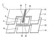
Now, be described in detail with reference to the attached drawings embodiments of the invention.Fig. 1,2A and 2B show the printed circuit board (PCB) according to first embodiment of the invention, and wherein Fig. 1 is plane graph, and Fig. 2 A shows the perspective view of two separated conductive layers, and Fig. 2 B only illustrates near the partial cross section figure of signal routing.Go out as shown in Figure 2 A, multilayer board 1 comprises the first conductive layer 21 and the second conductive layer 22.In addition, dielectric layer 20 is formed between the first conductive layer 21 and the second conductive layer 22.
The first frame ground pattern (hereinafter referred to as " a FG pattern ") 2 and first signal grounding pattern (hereinafter referred to as " a SG pattern ") 3 are formed in the first conductive layer 21.The one FG pattern 2 and a SG pattern 3 are by the first slotted section 4 and separated from one another.External interface assembly 6 such as connector or switch is installed on a FG pattern 2.The first semiconductor device 7, the second semiconductor device 9 and the 3rd semiconductor device 10 are installed on a SG pattern 3.External interface assembly 6 and the first semiconductor device 7 are connected to each other by crossing the signal routing 5 of the first slotted section 4.In addition, the second semiconductor device 9 and the 3rd semiconductor device 10 are connected to each other by signal routing 8.
In addition, the second frame ground pattern (hereinafter referred to as " the 2nd FG pattern ") 18 and secondary signal grounding pattern (hereinafter referred to as " the 2nd SG pattern ") 19 are formed in the second conductive layer 22 so that respectively with a FG pattern 2 and SG pattern 3 crossovers.The 2nd FG pattern 18 and the 2nd SG pattern 19 are by the second slotted section 34 and separated from one another.The link 23 and 24 that connects the 2nd FG pattern 18 and the 2nd SG pattern 19 be disposed in the second slotted section 34 at the part place extending across below the signal routing 5 of the first slotted section 4. Link 23 and 24 is arranged at homonymy not along signal routing 5, so that extend across the second slotted section 34.
The one FG pattern 2 and the 2nd FG pattern 18 pass through conductive component 11 and 12 by short circuit.In addition, a SG pattern 3 and the 2nd SG pattern 19 pass through conductive component 13,14,15 and 16 by short circuit. Conductive component 11,12,13,14,15 and 16 can form by through hole or non-penetrating via hole.In addition the screw that, multilayer board 1 is fixed to metal shell 17 can be used to conductive component 13,14,15 and 16.
In metal shell 17, suppose that ESD noise is applied near external interface assembly 6.As mentioned above, ESD noise flows in a FG pattern 2 and the 2nd FG pattern 18, and most ESD noise flows in metal shell 17 by conductor part 11 and 12.Yet a part of ESD noise flows in the 2nd SG pattern 19 by link 23 and 24.In this case, in the situation that two links with conductivity are set, ESD noise is divided into two parts, and the magnetic flux being produced by each link reduces.
In addition, the magnetic flux separately being produced by the first link 23 and the second link 24 therein magnetic flux has contrary component with the position of signal routing 5 interlinkages (link), therefore magnetic flux cancels each other out, and has reduced the magnetic flux with signal routing 5 interlinkages.Generally, due to the magnetic flux having reduced with signal routing 5 interlinkages, therefore reduced the ESD noise in semiconductor device 7 that flows to of being induced by signal routing 5, and improved the patience to static.
Now, with reference to figure 3, describe the principle that in multilayer board shown in Figure 1, ESD noise is propagated to signal routing 5 in detail.In Fig. 3, link 23 and 24 has identical width, and arranges symmetrically about signal routing 5.In Fig. 3, link 23 has the end 32 that position approaches link 24 most, and the direction of mobile ESD noise current is vertical paper direction backward in end 32.Arrow 34 represents by mobile ESD noise current in end 32 direction at the magnetic flux B1 of the midpoint generation of side contact with dielectric layer 20 of signal routing 5.It is vertical paper direction backward that link 24 has the direction that position approaches ESD noise current mobile in the 33, end 33, end of link 23 most.Arrow 35 represents by mobile ESD noise current in end 33 direction at the magnetic flux B2 of the midpoint generation of side contact with dielectric layer 20 of signal routing 5.Arrow 31 represents the direction of the resultant flux B ' of magnetic flux B1 and magnetic flux B2.
At this moment, due to the approaching result causing of link 23 and 24, in link 23 and 24, mobile ESD current noise is gathered in the end that approaches link 24 most 32 of link 23 and 33 places, the end that approaches link 23 most of link 24.Therefore, the principle about the mobile electric current in the end 33 of the end 32 at link 23 and link 24 by explanation.
The electromagnetic noise current (I) that is applied to a FG pattern 18 is divided into two electric currents by the first link 23 and the second link 24, and if the configuration of link 23 and 24 is mutually the same, in each link 23 and 24, the amplitude of mobile ESD noise current becomes I/2.In this case, be equal to each other with the magnetic flux B1 of signal routing 5 interlinkages and the amplitude of B2, and this amplitude is represented by formula (2) below.
Wherein h is the thickness of dielectric layer 130, and g is the width in the gap between link 23 and 24.θ is the angle being formed with the line that the end 33 of the end of link 23 32 and link 24 is connected by the line that the central point of the end of link 23 32 and signal routing 5 is connected.Because link 23 and 24 is arranged symmetrically about signal routing 5, by the line that the central point of the end of link 24 33 and signal routing 5 is connected, be therefore also θ with the angle that the line that the end 32 of the end of link 24 33 and link 23 is connected forms.
The resultant flux B ' of magnetic flux B1 and magnetic flux B2 is represented by formula (3) below.
Formula (3)
When revising formula (3), as represented in the formula by below (4), eliminate the composition of cos θ.
Formula (4)
The amplitude of resultant flux B ' is represented by formula (5) below according to formula (1)~(4).
The coefficient composition on the right side in the scope of 90 ° of 0 < θ < in formula (5) is represented by formula (6) below.
Meet formula (7) below.
| B ' | < | B| ... formula (7)
That is, the amplitude of the magnetic flux B in the configuration shown in the Amplitude Ratio Figure 11 of the resultant flux B ' in the configuration shown in discovery Fig. 3 is little.That is,, owing to can reducing to propagate into the ESD noise of signal routing, therefore can improve the patience to the ESD noise in printed circuit board (PCB).
(testing 1)
For the object of describing the advantage of the present embodiment, carry out the electromagnetic-field simulation of printed circuit board (PCB) shown in Figure 1.Fig. 4 shows the model using in electromagnetic-field simulation.In Fig. 4, represented by identical symbol with parts identical in Fig. 1.It is the rectangular shape that 100mm and minor face are 80mm that printed circuit board (PCB) 1 has long limit, and there is following structure, this structure there is the first conductive layer and the second conductive layer that thickness is 50 μ m and be placed in the first conductive layer and the second conductive layer between thickness be the dielectric layer that 200 μ m and dielectric constant are 4.3.Two links are that 2mm is wide, and about signal routing 5, arrange symmetrically in the situation that is 0.5mm of the gap between it.The one FG pattern 2 is separated by the first wide slotted section 4 of 2mm with a SG pattern 3.In addition, the 2nd FG pattern is also separated by the second wide slotted section of 2mm with the 2nd SG pattern.As wave source, the Gaussian pulse under the frequency of 0~3GHz with the intensity of 1W of simulation ESD noise is applied to a FG pattern 2.Each in signal routing 5 and 8 has long microstrip line (the micro strip line) structure of the wide and 30mm of 0.3mm, and ends at the first conductive layer 21 and have the resistance of 50 Ω.
Under these conditions, carry out emulation, and the ESD noise current that propagates into signal routing 5 obtaining in result shown in Fig. 5 A.In Fig. 5 A, axis of abscissas represents the time, and axis of ordinates represents the value of ESD noise current.
(comparative experiments 1)
For relatively, in the traditional printed circuit board (PCB) shown in Figure 10 A and Figure 10 B, as testing in 1, emulation propagates into the ESD noise current of signal routing 105.Comparative experiments 1 is with the difference of experiment 1, and the quantity that is arranged in the link on the second conductive layer 122 is one, and this link be positioned at signal routing 105 under.The width of link 120 is 2mm.The in the situation that of above-mentioned configuration, as carry out electromagnetic-field simulation testing in 1, and the ESD noise current that propagates into signal routing 105 obtaining in result shown in Fig. 5 B.When Fig. 5 A and Fig. 5 B are compared, little than in Fig. 5 B of the amount of finding the ESD noise current that propagates into signal routing 5 in Fig. 5 A.That is, as compared with comparative experiments 1, high to the patience of ESD noise in experiment 1.
In addition, the variation of mobile ESD noise current in the signal routing that emulation occurs when changing the layout of the first link 23 and the second link 24, and research is in the layout of link and reduce the relation between the effect of ESD noise current.Use the simulation model identical with the simulation model using in experiment 1.Change in the gap (r1) between signal routing 5 and the end 32 of the first link 23 and the gap (r2) between signal routing 5 and the end 33 of the second link 24, extends across ESD noise current mobile in the signal routing 5 of slotted section 4 to calculate.In this comparative experiments 1, link 23 and 24 has identical wiring width, and arranges symmetrically about signal routing 5.Therefore, gap is represented by common value r.
Result is illustrated in Fig. 5 C.In Fig. 5 C, axis of abscissas is the ratio of the thickness h of the dielectric layer while watching as the distance r of the above-mentioned common value cross section vertical with wiring direction from signal routing 5.Axis of ordinates be in hypothesis the ESD noise current in conventional art be 100 o'clock according to the slip of ESD noise current of the present invention.From Fig. 5 C, be appreciated that larger and obtain ESD noise decrease effect while being less than or equal to 7.5 times than the thickness h of dielectric layer apart from r.In addition, preferably, send out and when present range r is more than or equal to 1.1 times of thickness h of dielectric layer and is less than or equal to 5.0 times, to obtain 10% or higher ESD noise decrease effect.
In addition,, in this comparative experiments 1, two links 23 and 24 situations that have identical wiring width and be arranged symmetrically with about signal routing 5 of same conductive layer 22 wherein have been described.In this case, because the gap (r1) between signal routing 5 and the first link 23 and the gap (r2) between signal routing 5 and the second link 24 become, be equal to each other, therefore can eliminate the composition of the cos θ in above-mentioned formula (3) completely.That is, the vertical composition of the magnetic flux of Fig. 3 can be eliminated completely, and ESD noise current can be suppressed most effectively.
Yet, the invention is not restricted to wherein two links 23 and 24 configurations that there is identical wiring width and be arranged symmetrically with about signal routing 5, but can be applicable to other configuration, as long as above-mentioned larger and be less than or equal to 7.5 times than the thickness h of dielectric layer apart from r1 and r2.
In addition,, by link 23 and 24 being arranged in to the return current path of guaranteeing to extend across signal mobile in the signal routing 5 of slotted section 4 on the second conductive layer 22, therefore can maintain the inhibition to radiated noise.
(embodiment 2)
Fig. 6,7A and 7B show the printed circuit board (PCB) according to second embodiment of the invention, and wherein Fig. 6 is plane graph, and Fig. 7 A is the perspective view that two separated conductive layers are shown, and Fig. 7 B is near the partial cross section figure that signal routing is only shown.
The difference of the present embodiment and the first embodiment shown in Figure 1 is only, a FG pattern 2 and a SG pattern 3 are connected to each other by the 3rd link 25 with conductivity and the 4th link 26 in the first conductive layer 21.The 3rd link 25 and the 4th link 26 extend on the wiring direction of signal routing 5, and arrange symmetrically about signal routing 5.
Utilize four to there is the link 23,24,25 of conductivity and 26 configuration, compare with embodiment 1, further disperseed ESD noise, and further reduced the magnetic flux being produced by each link.In addition, by be arranged in magnetic flux that the 3rd link 25 on conductive layer 21 and the 4th link 26 produce therein those magnetic fluxs there is contrary component with the position of signal routing 5 interlinkages.Therefore, eliminate magnetic field, and reduced the magnetic flux with signal routing 5 interlinkages.Generally, the amount owing to can further reducing with the magnetic flux of signal routing 5 interlinkages, therefore reduces the ESD noise in semiconductor device 7 that flows to of being induced by signal routing 5, and further improves the patience to static.
(testing 2)
For the object of describing the advantage of embodiment 2, as testing in 1, carry out the electromagnetic-field simulation of multilayer board.
In experiment 2, except testing 1 configuration, also the 3rd link 25 and the 4th link 26 are arranged on the first conductive layer 21.The 3rd link 25 and the 4th link 26 are that 2mm is wide, and about signal routing 5, arrange be symmetrically 0.9mm in gap from the first conductive layer 21 in the situation that.Utilize above-mentioned configuration as tested in 1, to carry out electromagnetic-field simulation, and the ESD noise current that propagates into signal routing 5 that obtains of result shown in Figure 8.
When Fig. 8 and Fig. 5 A are compared, to find to compare with experiment 1, the amount that propagates into the ESD noise current of signal routing 5 in the configuration of experiment 2 is further reduced.That is, test 2 configuration and further improve the patience to ESD noise.
In this case, expectation, is arranged in two links 25 and 26 approach signal wiring as much as possible 5 on same conductive layer 21.In addition,, when the 3rd link 25 and the 4th link 26 have identical wiring width, improve the symmetry of the magnetic flux producing.Therefore, further improve the effect of eliminating magnetic field.
Although reference example embodiment has described the present invention, should be appreciated that and the invention is not restricted to disclosed exemplary embodiment.Thereby the scope of following claim comprises all such modifications, the structure being equal to and function by being given the widest explanation.
The application requires the rights and interests of the Japanese patent application No.2009-019297 submitting on January 30th, 2009 and the Japanese patent application No.2009-279911 submitting on December 9th, 2009, and the full content of above-mentioned two applications is incorporated in this by reference.
Claims (5)
1. a multilayer board, comprises:
The first conductive layer, described the first conductive layer comprises:
First signal grounding pattern;
The first frame ground pattern, external interface assembly is installed on the first frame ground pattern;
The first slotted section, described the first slotted section make first signal grounding pattern and the first frame ground pattern separated from one another; And
Signal routing, described signal routing is arranged as and extends across the first slotted section;
The second conductive layer, described the second conductive layer is layered on the first conductive layer by dielectric layer, and described the second conductive layer comprises:
Secondary signal grounding pattern;
The second frame ground pattern;
The second slotted section, described the second slotted section make secondary signal grounding pattern and the second frame ground pattern separated from one another; And
The first link and the second link, for secondary signal grounding pattern and the second frame ground pattern are connected to each other,
Wherein along signal routing, at homonymy not, arrange the first link and the second link, make the first link and the second link clip signal routing and extend across the second slotted section,
Wherein, in the vertical cross section of the wiring direction with signal routing, in the mid point that contacts a side with dielectric layer of signal routing and the position of the first link, approach the distance between the end of the second link most and in the position of described mid point and the second link, approach 7.5 times that distance between the end of the first link is all greater than the thickness of described dielectric layer and is less than or equal to described thickness most.
2. multilayer board according to claim 1, wherein the first link and the second link have identical wiring width, and place symmetrically about signal routing.
3. multilayer board according to claim 1, wherein, in the vertical cross section of the wiring direction with signal routing, in the mid point that contacts a side with dielectric layer of signal routing and the position of the first link, approach the distance between the end of the second link most and in the position of described mid point and the second link, approach 5.0 times of thickness that distance between the end of the first link is all more than or equal to 1.1 times of thickness of described dielectric layer and is less than or equal to described dielectric layer most.
4. multilayer board according to claim 1,
Wherein first signal grounding pattern is connected with the 4th link by the 3rd link with the first frame ground pattern, and
Wherein the 3rd link and the 4th link are arranged at homonymy not symmetrically along signal routing, make the 3rd link and the 4th link clip signal routing and extend across the first slotted section.
5. multilayer board according to claim 4, wherein the 3rd link and the 4th link have identical wiring width.
Applications Claiming Priority (5)
| Application Number | Priority Date | Filing Date | Title |
|---|---|---|---|
| JP2009-019297 | 2009-01-30 | ||
| JP2009019297 | 2009-01-30 | ||
| JP2009279911A JP5409312B2 (en) | 2009-01-30 | 2009-12-09 | Multilayer printed circuit board |
| JP2009-279911 | 2009-12-09 | ||
| PCT/JP2010/051547 WO2010087506A1 (en) | 2009-01-30 | 2010-01-28 | Multilayer printed circuit board |
Publications (2)
| Publication Number | Publication Date |
|---|---|
| CN102293068A CN102293068A (en) | 2011-12-21 |
| CN102293068B true CN102293068B (en) | 2014-03-05 |
Family
ID=42026336
Family Applications (1)
| Application Number | Title | Priority Date | Filing Date |
|---|---|---|---|
| CN201080005398.8A Expired - Fee Related CN102293068B (en) | 2009-01-30 | 2010-01-28 | Multilayer printed circuit board |
Country Status (4)
| Country | Link |
|---|---|
| US (1) | US8530750B2 (en) |
| JP (1) | JP5409312B2 (en) |
| CN (1) | CN102293068B (en) |
| WO (1) | WO2010087506A1 (en) |
Families Citing this family (9)
| Publication number | Priority date | Publication date | Assignee | Title |
|---|---|---|---|---|
| TW201316895A (en) * | 2011-10-14 | 2013-04-16 | Hon Hai Prec Ind Co Ltd | Printed circuit board capable of preventing electromagnetic interface |
| JP5348259B2 (en) * | 2012-02-02 | 2013-11-20 | 横河電機株式会社 | Insulation circuit and communication equipment |
| US8913401B2 (en) | 2012-11-14 | 2014-12-16 | Fuji Xerox Co., Ltd. | Multilayer wiring board |
| JP5803961B2 (en) * | 2013-03-21 | 2015-11-04 | 株式会社豊田自動織機 | Substrate spacing member and inverter device |
| WO2015140856A1 (en) * | 2014-03-18 | 2015-09-24 | パナソニックIpマネジメント株式会社 | Electronic apparatus |
| JP6399969B2 (en) * | 2015-05-22 | 2018-10-03 | 三菱電機株式会社 | Printed board |
| JP7373705B2 (en) * | 2018-02-15 | 2023-11-06 | パナソニックIpマネジメント株式会社 | circuit boards, electronic equipment |
| KR102616482B1 (en) | 2018-07-26 | 2023-12-26 | 삼성전자주식회사 | printed circuit board including a ground wiring for canceling the electromagnetic wave generated in the power wiring and electronic device with the same |
| CN115175441B (en) * | 2022-08-01 | 2024-03-12 | 哈尔滨理工大学 | Vacuum low dielectric constant and low conductivity micro-current transmission circuit board |
Family Cites Families (9)
| Publication number | Priority date | Publication date | Assignee | Title |
|---|---|---|---|---|
| JPH10208791A (en) * | 1997-01-21 | 1998-08-07 | Canon Inc | Connecting method for inter-frame grounds in casing |
| JPH11177274A (en) * | 1997-12-08 | 1999-07-02 | Canon Inc | Method for connecting printed wiring board and cable and box-like body, and electronic apparatus |
| JP3703362B2 (en) * | 2000-03-14 | 2005-10-05 | キヤノン株式会社 | Electronics |
| US6573804B2 (en) * | 2000-03-14 | 2003-06-03 | Canon Kabushiki Kaisha | Electronic apparatus having a printed circuit board with multi-point grounding |
| US6507495B1 (en) * | 2000-06-28 | 2003-01-14 | Dell Products L.P. | Three-dimensional technique for improving the EMC characteristics of a printed circuit board |
| US6937480B2 (en) | 2001-05-14 | 2005-08-30 | Fuji Xerox Co., Ltd. | Printed wiring board |
| JP2003163467A (en) * | 2001-05-14 | 2003-06-06 | Fuji Xerox Co Ltd | Printed wiring board and device for aiding design of printed wiring board |
| KR100731544B1 (en) * | 2006-04-13 | 2007-06-22 | 한국전자통신연구원 | Multi-metal coplanar waveguide |
| JP5025376B2 (en) * | 2006-09-11 | 2012-09-12 | キヤノン株式会社 | Printed wiring board and electronic device |
-
2009
- 2009-12-09 JP JP2009279911A patent/JP5409312B2/en not_active Expired - Fee Related
-
2010
- 2010-01-28 US US13/140,094 patent/US8530750B2/en not_active Expired - Fee Related
- 2010-01-28 CN CN201080005398.8A patent/CN102293068B/en not_active Expired - Fee Related
- 2010-01-28 WO PCT/JP2010/051547 patent/WO2010087506A1/en active Application Filing
Also Published As
| Publication number | Publication date |
|---|---|
| JP2010199553A (en) | 2010-09-09 |
| US20110247869A1 (en) | 2011-10-13 |
| JP5409312B2 (en) | 2014-02-05 |
| US8530750B2 (en) | 2013-09-10 |
| WO2010087506A1 (en) | 2010-08-05 |
| CN102293068A (en) | 2011-12-21 |
Similar Documents
| Publication | Publication Date | Title |
|---|---|---|
| CN102293068B (en) | Multilayer printed circuit board | |
| US6420778B1 (en) | Differential electrical transmission line structures employing crosstalk compensation and related methods | |
| JP5194440B2 (en) | Printed wiring board | |
| CN103120038B (en) | Structure and wiring substrate | |
| KR20060041676A (en) | Variable resonator and variable phase shifter | |
| US8053679B2 (en) | Printed circuit board | |
| US7667980B2 (en) | Printed circuit boards for countering signal distortion | |
| US6717494B2 (en) | Printed-circuit board, coaxial cable, and electronic device | |
| JP6211835B2 (en) | High frequency transmission line | |
| CN102098866A (en) | Printed circuit board | |
| US6677832B1 (en) | Connector for differential-mode transmission line providing virtual ground | |
| WO2021192073A1 (en) | Circuit board and electronic device | |
| CN1275351C (en) | Surface mounted broadside directional coupler | |
| WO2012039120A2 (en) | Printed circuit board | |
| EP1568099B1 (en) | A circuit that taps a differential signal | |
| US7049901B2 (en) | Parallel plate wave-guide structure in a layered medium for transmitting complementary signals | |
| CN113473724B (en) | Printed circuit board and wiring method thereof | |
| JPH1056245A (en) | Printed wiring board | |
| US20150102870A1 (en) | Directional coupler arrangement and method | |
| WO2022219709A1 (en) | Wiring board | |
| JP2014203689A (en) | Connector, circuit board, and electronic apparatus | |
| WO2023204099A1 (en) | Multilayer substrate | |
| Duan et al. | Study on Ground Plane Optimization of PCB Design for HDI Power System | |
| Selezinski et al. | Routing Length Impact on Differential Via Crosstalk Cancellation | |
| JP2004296250A (en) | Modular connector |
Legal Events
| Date | Code | Title | Description |
|---|---|---|---|
| C06 | Publication | ||
| PB01 | Publication | ||
| C10 | Entry into substantive examination | ||
| SE01 | Entry into force of request for substantive examination | ||
| GR01 | Patent grant | ||
| GR01 | Patent grant | ||
| CF01 | Termination of patent right due to non-payment of annual fee | ||
| CF01 | Termination of patent right due to non-payment of annual fee |
Granted publication date: 20140305 Termination date: 20210128 |