CN1275351C - Surface mounted broadside directional coupler - Google Patents
Surface mounted broadside directional coupler Download PDFInfo
- Publication number
- CN1275351C CN1275351C CNB028183193A CN02818319A CN1275351C CN 1275351 C CN1275351 C CN 1275351C CN B028183193 A CNB028183193 A CN B028183193A CN 02818319 A CN02818319 A CN 02818319A CN 1275351 C CN1275351 C CN 1275351C
- Authority
- CN
- China
- Prior art keywords
- coupler
- tooth
- circuit board
- strip conductor
- right track
- Prior art date
- Legal status (The legal status is an assumption and is not a legal conclusion. Google has not performed a legal analysis and makes no representation as to the accuracy of the status listed.)
- Expired - Fee Related
Links
Images


Classifications
-
- H—ELECTRICITY
- H01—ELECTRIC ELEMENTS
- H01P—WAVEGUIDES; RESONATORS, LINES, OR OTHER DEVICES OF THE WAVEGUIDE TYPE
- H01P5/00—Coupling devices of the waveguide type
- H01P5/12—Coupling devices having more than two ports
- H01P5/16—Conjugate devices, i.e. devices having at least one port decoupled from one other port
- H01P5/18—Conjugate devices, i.e. devices having at least one port decoupled from one other port consisting of two coupled guides, e.g. directional couplers
- H01P5/184—Conjugate devices, i.e. devices having at least one port decoupled from one other port consisting of two coupled guides, e.g. directional couplers the guides being strip lines or microstrips
- H01P5/187—Broadside coupled lines
Abstract
A directional coupler comprises a coupler circuit board which is mounted substantially perpendicular to the surface of a parent circuit board. First and second upper traces are disposed on the opposing surfaces of the coupler circuit board. The coupling between the upper electrically conductive traces determines the odd mode impedance of the coupler. First and second lower traces are also disposed on opposing surfaces and connected to ground. The upper and lower traces are arranged such that the even mode of the impedance is determined by the coupling between the first upper trace and the second lower trace and the coupling between the second upper trace and the first lower trace.
Description
Technical field
The present invention relates to a kind of quarter-wave directional coupler of TEM pattern, especially, relate to a kind of like this coupler that the coupling line element is arranged, wherein kind of thread elements is placed on the opposite side of circuit board, and the material that is independent of female circuit board of placing this coupler and forms this circuit board decides the parity mode impedance of coupler.
Background technology
Directional coupler is four port devices, as the power divider or the synthesizer of electromagnetic transmission.These four ports are called port one, port 2, port 3 and port 4 respectively.When to the port one input signal, this signal is coupled to port 2 and 3, but is not coupled to port 4.Similarly, the signal of input port 4 is coupled to port 2 and 3 but be not coupled to port one.Because not coupling between port one and 4, these ports are called non-coupling or the separate port with respect to the other side.Signal can be imported, perhaps owing to reflect entry port 2 and 3.The signal of input port 2 is coupled to port one and 4, but is not coupled to port 3, and the signal of input port 3 is coupled to port one and 4, but is not coupled to port 2.Therefore, port 2 and 3 is separate ports.
At United States Patent (USP) 5,539, the directional coupler of Michael J.Culling is disclosed in 362, it is transferred to the identical assignee of the application.This coupler comprises a coupler electricity dielectric plate, and it stands upright on the upper surface of female circuit board.There is the conducting element up and down of square interdigitated tooth to be placed on each face of coupler dielectric plate.Lead is placed on the upper surface of female circuit board and is connected to the two ends of the last conducting element of every side.Following conducting element ground connection.
Odd mode impedance in the directional coupler is two and goes up the function that is coupled between the conducting element.The most of electric field relevant with odd mode impedance passes the coupler dielectric plate.Even mode impedance is the function that is coupled between the conducting element up and down of coupler dielectric plate homonymy.Therefore, the major part of the electric field relevant with even mode impedance is passed the air of panel area.
The differing dielectric constant values of dielectric plate and air has caused the different phase velocities between the field, thereby causes worse coupler directionality and narrower bandwidth.Square shaped teeth in the Culling device is intended to propagation delay by balanced each pattern and compensates difference between the phase velocity.The ripple relevant with even mode impedance wriggles between the slit that is formed by tooth.The increase of effective channel length is enough to proofread and correct the difference of effective speed.
Summary of the invention
Yet, on quantity that is used to postpone the tooth that fast wave propagates and size, have actual restriction.Therefore, the Culling device can't be proofreaied and correct dielectric validity that the high dielectric constant coefficient is arranged.Provide a cover can compensate phase velocity and with the irrelevant system of the dielectric constant of material be desirable.
According to an aspect of of the present present invention, directional coupler comprises a coupler circuit board, and it is vertically mounted on the upper surface of female circuit board basically.First and second get on the right track (trace) be placed on the apparent surface of coupler circuit board.Coupling between the last strip conductor has determined the odd mode impedance of coupler.First and second lower railway (trace) also are placed on apparent surface and ground connection.So place go up lower railway in case by first get on the right track and second lower railway between coupling and second get on the right track and first lower railway between coupling decide even mode impedance.
According to another aspect of the present invention, directional coupler comprises a coupler circuit board, and it is vertically mounted on the surface of female circuit board basically.First and second strip conductors are placed on the apparent surface of coupler circuit board.Strip conductor has a straight top margin and a base on first, has placed many teeth on the base.Strip conductor also has a straight top margin and a base on second, has also placed many teeth on the base and has apart from first the skew of tooth on getting on the right track.Last strip conductor electric coupling causes that coupler shows odd mode impedance, and it is by the width decision of track.This impedance is the coupling factor of coupler requirement and the function of characteristic impedance.
First and second times strip conductors also are placed on the apparent surface of coupler circuit board.Each described down strip conductor and getting on the right track separately separately.First lower railway has a straight base and a top margin, has many with respect to the first staggered tooth of tooth that gets on the right track on the base on the top margin.The tooth that these teeth get on the right track in side in alignment second is so that the zone that is covered by the tooth of first lower railway is overlapping with the area part ground that is illustrated in second outstanding on the coupler circuit board surface that comprises first lower railway tooth position of getting on the right track.Second lower railway also has a straight base and a top margin, has many with respect to the second staggered tooth of tooth that gets on the right track on the base on the top margin.The tooth that these teeth get on the right track in side in alignment first is so that the zone that is covered by the tooth of second lower railway is overlapping with the area part ground that is illustrated in first outstanding on the coupler circuit board surface that comprises second lower railway tooth position of getting on the right track.
First gets on the right track is electrically coupled to second lower railway, and second gets on the right track is electrically coupled to first lower railway.This causes that coupler shows the even mode impedance by the overlapping region decision of tooth.The variation of this resistance value is the desired coupling factor of coupler and the function of characteristic impedance.
Description of drawings
For the people who is familiar with correlation technique of the present invention, based on the following description of the present invention with reference to accompanying drawing, the aforesaid feature with other of the present invention will be conspicuous, and wherein accompanying drawing comprises:
Fig. 1 is according to a kind of directional coupler of the present invention;
Fig. 2 is the end view of the first surface of coupler PCB;
Fig. 3 is the end view of the second surface of coupler PCB;
Fig. 4 be expression with the coupler first surface on the first relevant end view that gets on the right track of extrusion position of second lower railway;
Fig. 5 is according to the sectional view of directional coupler of the present invention at the tooth overlapping of first tooth that gets on the right track and second lower railway;
Fig. 6 is the sectional view of prior art directional coupler, expression odd mode impedance Z
OoElectric field;
Fig. 7 is the sectional view of prior art directional coupler, expression even mode impedance Z
OeElectric field;
Fig. 8 is the sectional view according to directional coupler of the present invention, is illustrated in the odd mode impedance Z of the tooth overlapping of first tooth that gets on the right track and second lower railway
OoElectric field;
Fig. 9 is the sectional view according to directional coupler of the present invention, is illustrated in the even mode impedance Z of the tooth overlapping of first tooth that gets on the right track and second lower railway
OeElectric field;
Figure 10 is the sectional view according to directional coupler of the present invention, is illustrated in the even mode impedance Z of the tooth overlapping of second tooth that gets on the right track and first lower railway
OeElectric field.
Embodiment
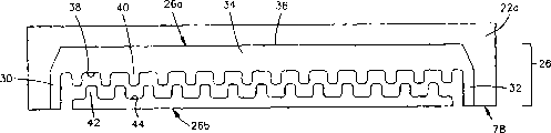
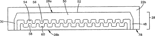
Shown in Fig. 1-5 is according to directional coupler 20 of the present invention.This coupler 20 comprises a coupler circuit board 22 that plane 22a and 22b are arranged.In illustrative examples, coupler circuit board 22 is printed circuit board (PCB) (PCB).Printed circuit board (PCB) is on record in the prior art, and coupler circuit board 22 can use any suitable method to make.Coupler 20 is installed on female circuit board 24 of plane 24a and 24b.Install coupler 20 make it plane 22a and 22b perpendicular to the plane 24a and the 24b of female circuit board 24.Though other peripheral circuit relevant with the circuit that uses coupler 20 do not draw in Fig. 1-5, is installed on female circuit board 24 yet.
The second staggered coupling element 28 is placed on the plane 22b opposite with the first staggered coupling element 26.The second staggered coupling element 28 comprises one second get on the right track 28a and one second lower railway 28b.Second 28a that gets on the right track comprises two side sections 46 and 48, and they are connected respectively to an end that the vertical section 50 of predetermined length and width is arranged.There are a straight top edge 52 and a lower limb 54 that comprises tooth 56 in this vertical section 50.With tooth 56 with staggered mode staggered be the tooth 58 that on the top edge 60 of the second lower railway 28b, forms.
As shown in Figure 4, at the place, plane by coupler PCB22 center, the first and second staggered coupling elements 26 and 28 are not symmetrical.First position of vertical section 34 top edges 36 of getting on the right track 26a is consistent with second position of vertical section 50 top edges 52 of getting on the right track 28a on being positioned at coupler PCB22 opposite side.Yet, in first tooth 56 phase deviations of getting on the right track and forming on the tooth 40 that forms on the lower limb 38 of 26a and the lower limb 54 at the second track 28a.Therefore, tooth 58 phase deviations that on tooth 42 that forms on the top edge 44 of the first lower railway 26b and top edge 60, form at the second lower railway 28b.Thereby 26a and 28a and their lower railway 26b and the 28b separately that get on the right track keeps staggered, but places lower railway 26b and 28b so that their tooth 42 and 58 and at tooth 40 or the 56 locational protruding overlaids of the get on the right track 26a or the 28a of PCB22 opposite side.This is overlapping is represented by the dotted line among Fig. 4.
Also have some strip conductors to be placed on and be beneficial to assemble coupler 20 on female circuit board.On the 24a of the plane of female circuit board 24, placing four strip conductors 62,64,66,68.These tracks 62,64,66,68 are provided to the side section 30,32,46 of get on the right track 26a and 28a and 48 direct the connection respectively with the end effect of minimum.This provides good impedance matching between strip conductor and the side section that links to each other with it.Except strip conductor 62,64,66 and 68, also have two ground planes 70 and 72 also to be placed on the plane 24a of female circuit board 24.This ground plane is identical with the width of lower railway 26b and 28b.On the 24b of the plane of female circuit board 24, place a following ground plane 74.Each ground plane 70 and 72 is connected to this time ground plane 74 by a large amount of through holes 76.This time ground plane 74 is connected to the system earth current potential, and through hole 76 causes ground plane 70 and 72 also to be in the system earth current potential.
Be welded in place strip conductor by the strip conductor that will be positioned at coupler PCB22, directional coupler 20 is connected on female circuit board 24 in female circuit board.Lower limb 78 places at coupler PCB22 are welded to strip conductor 62 and 64 respectively with side section 30 and 32.Similarly, at lower limb 78 places side section 46 and 48 is welded to strip conductor 66 and 68 respectively.At lower limb 78 places the first lower railway 26b is welded to ground plane 70, and the second lower railway 28b is welded to ground plane 72 at lower limb 78 places.All these plumb joints have formed protruding pad 80.Can use other method, for example suitable electroconductive binder replaces protruding pad 80.
In the welding or the process of other method of attachment, can use the pilot nail (not shown) to realize suitable mechanically calibrated of coupler PCB22.Each pilot nail is corresponding to an installing hole (not shown) on female circuit board 24.Use known " picking and placeing " mounting technology easily to finish automatically to use pilot nail to calibrate and use protruding pad 80 to carry out mechanical connection and electrical connection.
The electrical characteristics of directional coupler 20 are by the coupling factor C decision of coupler.Flow through when getting on the right track 26a and 28a with identical direction when the electric current of identical size, between each element and ground connection, have one and be called Z
OeEven mode impedance.Similarly, flow through when getting on the right track 26a and 28a with opposite direction, between each element and ground connection, have one and be called Z when the electric current of identical size
OoOdd mode impedance.The even mould and the odd mode impedance of the line that one coupling is right are provided by following formula:
Wherein C is a coupling factor, Z
oIt is the characteristic impedance (for example, strip conductor 62-68) of the transmission line of coupler 20 connections.Formula (1) and (2) expression coupling factor C and requirement realize the parity mode impedance Z of this coupling factor
OoAnd Z
OeBetween functional relation.
The parity mode impedance Z is supposed in formula (1) and (2)
OoAnd Z
OeRelevant phase velocity of wave equates.But can not always so suppose, because the material that ripple passes has remarkable influence to phase velocity of wave.The general equation of phase velocity is:
Wherein c is the light velocity (for example 3 * 10 in the free space
8Meter per second), ε
EffIt is dielectric effective dielectric constant of propagating electric field.
Fig. 6 and 7 is illustrated in the propagation of the electric field (86 and 88) of parity mode impedance in the prior art equipment.Usually the strongest along the shortest grounding path electric field because per unit apart from the situation of potential change maximum under charged particle stressed the strongest.Shown in equipment 20 ' in, the grounding path (Fig. 6) that the electric field of even mode impedance 86 is the shortest is positioned at going up between (for example 26a ') and time (for example 26b ') track of this equipment one side.Therefore, an electric field part is in coupler board 22 ' middle propagation, and a part is propagated in air.Like this, the effective dielectric constant ε eff of electric field process drops on ε
rDIELECTRIC CONSTANT with air
0Between.Similarly, the electric field 88 (Fig. 7) of odd mode impedance gets on the right track the strongest between 26a ' and the 26b ' at two.Therefore, electric field is mainly in coupler board 22 ' middle propagation, the effective dielectric constant ε of process
EffApproach the relative dielectric constant ε of coupler board
rThis value significantly is different from the dielectric constant of the electric field process of even mode impedance.
When the phase velocity of two electric fields does not wait, be necessary to proofread and correct this difference.Otherwise the bandwidth of directional coupler and directionality can be adversely affected.In the prior art, this can cause it to realize through bigger coverage by the path of ripple through curling up that forces higher phase velocity.Therefore, two wave propagations are postponed comparably.When coupler board 22 ' use high dielectric constant materials was made, this method was not very effective.Regrettably, the material that being used to of many common, inexpensive made printed circuit board (PCB) has very high dielectric constant values, so that can't not proofread and correct when performance is significantly lost.Like this, must use more expensive material.
The present invention proofreaies and correct different phase velocity through PCB22 to the propagation of ground connection by regulating even mould electric field 86.Shown in Fig. 8-10, the lip-deep tooth of PCB (for example 40 and 42) is with respect to another lip-deep tooth (for example 56 and 58) skew, makes the last toothed portion of itself and opposite side overlapping so that place the lower tooth of each side.The thickness that it should be noted that PCB22 herein is usually less than the distance between the upper and lower track of every side (for example 26a and 26b).Therefore, the short circuit ground distance of even mould electric field 90 be one from last tooth (for example 40) by the path of PCB22 to the lower tooth of opposite side (for example 58).The dielectric constant of electric field 90 processes of even mode impedance is similar to the dielectric constant of electric field 88 processes of odd mode impedance like this.Therefore, two electric fields 88 and 90 phase velocity equate fully, and irrelevant with the dielectric constant of the material that is used to make coupler PCB22.
Should be pointed out that according to required coupler characteristics length and width and the teeth size of last strip conductor 26a and 28a and following strip conductor 26b and 28b are variable.For example, can change the width of going up strip conductor 26a and 28a.The variation of these width has changed two coupled characteristics that get on the right track between 26a and the 28a, has correspondingly changed the odd mode impedance of coupler 20.Similarly, can change tooth 40,42,56 on get on the right track 26a and 28a and lower railway 26b and the 28b and 58 size and shape, to increase or to reduce overlapping between the tooth on the coupler PCB22 both sides.The variable effect of overlapping region get on the right track 26a and 28a to relative lower railway 26b and the coupling between the 28b, thereby influenced the even mode impedance of coupler 20.The coupling factor that has changed coupler in the even mould or this variation in the odd mode impedance of coupler.Also can regulate the length of get on the right track 26a and 28a and lower railway 26b and 28b.These length convert as the function of coupler 20 required operating frequencies.
From foregoing description of the present invention, those who are familiar with known technology will figure out improvement, variation and modification.Enclose claims, be intended to comprise this improvement, variation and modification in being skilled in technique.
Claims (7)
1. plate side positioning coupler, it comprises:
The female circuit board that relative conductive surface is arranged;
Coupler circuit board that forms by backing material with apparent surface, and the mode that is basically perpendicular to one of the apparent surface of described female circuit board with its apparent surface is installed on described female circuit board;
Be installed in strip conductor on first and second on the apparent surface of described coupler circuit board respectively, described go up strip conductor by described coupler circuit board backing material electric coupling together so that described coupler shows odd mode impedance, the coupling factor that this impedance requires by the width decision of track and as coupler and the function of characteristic impedance and change; And
Be installed in first and second times strip conductors on the apparent surface of described coupler circuit board respectively, each described strip conductor down and last strip conductor separately are separately, wherein on described spacing between strip conductor and their the following strip conductors separately greater than the distance between the apparent surface of described coupler circuit board, described first and second times strip conductors are electrically connected to the system earth current potential, strip conductor is electrically coupled to described second time strip conductor by described coupler circuit board backing material on described first, and strip conductor is electrically coupled to described first lower railway by described coupler circuit board backing material on described second.
2. a directional coupler as being stated in the claim 1, the relative dielectric constant of wherein said coupler circuit board equals the relative dielectric constant of female circuit board.
3. a directional coupler as being stated in the claim 1, it has a required operating frequency, and the length of the wherein said first and second upper and lower strip conductors decides as the function of required operating frequency.
4. a directional coupler as being stated in the claim 1, wherein said coupler circuit board is a printed circuit board (PCB).
5. the plate side positioning coupler as being stated in the claim 1, wherein:
The base that strip conductor has a straight top margin and places many teeth above one on described first, and the base that strip conductor has a straight top margin and places many teeth above on described second, this base has apart from the skew that is placed on the tooth on the strip conductor on described first, described go up strip conductor by electric coupling so that described coupler shows odd mode impedance, the coupling factor that this impedance requires by the width decision of track and as coupler and the function of characteristic impedance and change; And
Each described down strip conductor and getting on the right track separately separately, described first time strip conductor has a straight base and a top margin, have many on the top margin with respect to being placed on the staggered tooth of the tooth on the strip conductor base on described first, described tooth is at described second tooth that gets on the right track of side in alignment, so that it is overlapping with the area part ground of the tooth position that is illustrated in described second lower railway outstanding on the described coupler circuit board first surface by the zone that described first tooth that gets on the right track covers, and described second time strip conductor has a straight base and a top margin, have many on the top margin with respect to the described second staggered tooth of tooth that gets on the right track on the base, the tooth that described tooth gets on the right track in side in alignment first, so that it is overlapping with the area part ground of the tooth position that is illustrated in described first lower railway outstanding on the described coupler circuit board second surface by the zone that described second tooth that gets on the right track covers, strip conductor is electrically coupled to that strip conductor is electrically coupled to described first lower railway on described second time strip conductor and described second on described first, so that described coupler shows even mode impedance, this impedance is the coupling factor that requires of coupler and the function of characteristic impedance by the variation of decision of the overlapping region of tooth and resistance value;
Be characterised in that described first get on the right track and described second lower railway on place the tooth of equal number, described second get on the right track and described first lower railway on place the tooth of equal number, and be placed on described first the quantity of tooth on getting on the right track more than being placed on described second the quantity of tooth on getting on the right track.
6. a directional coupler as being stated in the claim 5, the relative dielectric constant of wherein said coupler circuit board equals the relative dielectric constant of female circuit board.
7. a directional coupler as being stated in the claim 5, it has a required operating frequency, and the length of the wherein said first and second upper and lower strip conductors decides as the function of required operating frequency.
Applications Claiming Priority (2)
| Application Number | Priority Date | Filing Date | Title |
|---|---|---|---|
| US09/932,390 | 2001-08-17 | ||
| US09/932,390 US6590472B2 (en) | 2001-08-17 | 2001-08-17 | Surface mounted broadside directional coupler |
Publications (2)
| Publication Number | Publication Date |
|---|---|
| CN1555592A CN1555592A (en) | 2004-12-15 |
| CN1275351C true CN1275351C (en) | 2006-09-13 |
Family
ID=25462234
Family Applications (1)
| Application Number | Title | Priority Date | Filing Date |
|---|---|---|---|
| CNB028183193A Expired - Fee Related CN1275351C (en) | 2001-08-17 | 2002-08-12 | Surface mounted broadside directional coupler |
Country Status (7)
| Country | Link |
|---|---|
| US (1) | US6590472B2 (en) |
| EP (1) | EP1451889B1 (en) |
| CN (1) | CN1275351C (en) |
| AU (1) | AU2002356024A1 (en) |
| DE (1) | DE60229551D1 (en) |
| RU (1) | RU2265260C1 (en) |
| WO (1) | WO2003017414A2 (en) |
Families Citing this family (9)
| Publication number | Priority date | Publication date | Assignee | Title |
|---|---|---|---|---|
| US6903625B2 (en) * | 2003-10-16 | 2005-06-07 | Northrop Grumman Corporation | Microstrip RF signal combiner |
| DE102006038029A1 (en) * | 2006-08-14 | 2008-02-21 | Rohde & Schwarz Gmbh & Co. Kg | directional coupler |
| CN101009396B (en) * | 2007-01-18 | 2010-11-10 | 华为技术有限公司 | Directional coupler and the device with the same |
| KR101084249B1 (en) * | 2009-12-24 | 2011-11-17 | 삼성전기주식회사 | Printed circuit board and transmitting/receiving module including the same |
| TW201611552A (en) * | 2014-09-09 | 2016-03-16 | 鴻海精密工業股份有限公司 | Signal splitter and front-end circuit |
| RU2585884C1 (en) * | 2015-03-11 | 2016-06-10 | Федеральное государственное бюджетное образовательное учреждение высшего профессионального образования "Томский государственный университет систем управления и радиоэлектроники" | Trans-directed splitter on coupled lines with vertical board |
| RU189725U1 (en) * | 2019-03-27 | 2019-05-31 | Федеральное государственное бюджетное образовательное учреждение высшего образования "Томский государственный университет систем управления и радиоэлектроники" (ТУСУР) | UHF PHASE CONVERTER OF THE REFLECTIVE TYPE |
| RU196375U1 (en) * | 2019-07-11 | 2020-02-26 | Федеральное государственное автономное образовательное учреждение высшего образования "Уральский федеральный университет имени первого Президента России Б.Н. Ельцина" | COMPACT DIRECTED TAP |
| CN113904088B (en) * | 2021-11-08 | 2023-04-07 | 南京邮电大学 | Design method of ultra-wideband power divider based on vertical mounting substrate |
Family Cites Families (2)
| Publication number | Priority date | Publication date | Assignee | Title |
|---|---|---|---|---|
| JPS6313502A (en) * | 1986-07-04 | 1988-01-20 | Yuniden Kk | Microwave directional coupler |
| US5539362A (en) | 1995-06-30 | 1996-07-23 | Harris Corporation | Surface mounted directional coupler |
-
2001
- 2001-08-17 US US09/932,390 patent/US6590472B2/en not_active Expired - Lifetime
-
2002
- 2002-08-12 RU RU2004107656/09A patent/RU2265260C1/en not_active IP Right Cessation
- 2002-08-12 EP EP02794859A patent/EP1451889B1/en not_active Expired - Fee Related
- 2002-08-12 DE DE60229551T patent/DE60229551D1/en not_active Expired - Lifetime
- 2002-08-12 CN CNB028183193A patent/CN1275351C/en not_active Expired - Fee Related
- 2002-08-12 WO PCT/US2002/025198 patent/WO2003017414A2/en not_active Application Discontinuation
- 2002-08-12 AU AU2002356024A patent/AU2002356024A1/en not_active Abandoned
Also Published As
| Publication number | Publication date |
|---|---|
| CN1555592A (en) | 2004-12-15 |
| US6590472B2 (en) | 2003-07-08 |
| US20030034856A1 (en) | 2003-02-20 |
| RU2004107656A (en) | 2005-10-10 |
| WO2003017414A3 (en) | 2003-10-30 |
| RU2265260C1 (en) | 2005-11-27 |
| EP1451889A2 (en) | 2004-09-01 |
| EP1451889A4 (en) | 2004-09-08 |
| DE60229551D1 (en) | 2008-12-04 |
| EP1451889B1 (en) | 2008-10-22 |
| AU2002356024A1 (en) | 2003-03-03 |
| WO2003017414A2 (en) | 2003-02-27 |
Similar Documents
| Publication | Publication Date | Title |
|---|---|---|
| CN102293068B (en) | Multilayer printed circuit board | |
| EP2446508B1 (en) | Methods and apparatus for a grounding gasket | |
| US3689865A (en) | Connector | |
| US20110100682A1 (en) | Differential signal transmission cable | |
| CN1275351C (en) | Surface mounted broadside directional coupler | |
| JP2008262932A (en) | Crosstalk reduction for electrical connector | |
| EP2605624A1 (en) | Flexible flat cable | |
| US8053679B2 (en) | Printed circuit board | |
| JP3397707B2 (en) | Substrate with shield plane with various aperture patterns for transmission time and impedance control | |
| CN101448361B (en) | Printed circuit board, display apparatus having a printed circuit board and method of manufacturing the printed circuit board | |
| JPH10200311A (en) | Coplanar waveguide line with back ground conductor | |
| US20050001695A1 (en) | Microstrip coupler | |
| CN1412886A (en) | Coplanar directional coupler for mixed geometrical form | |
| EP0783773B1 (en) | Surface mounted directional coupler | |
| EP1568099B1 (en) | A circuit that taps a differential signal | |
| US7049901B2 (en) | Parallel plate wave-guide structure in a layered medium for transmitting complementary signals | |
| JPH08508134A (en) | Connecting rear wall for subrack | |
| US7828603B1 (en) | Electrical connector with crosstalk compensation | |
| WO2022219709A1 (en) | Wiring board | |
| CN2559181Y (en) | Printed circuit board | |
| TWI761287B (en) | Magnetic induction structure | |
| US20230132991A1 (en) | Signal transmission device | |
| JP2001035612A (en) | Fpc/ffc connector | |
| JP4136327B2 (en) | Electromagnetic wave generator | |
| CN115275715A (en) | Transmission plate and connector |
Legal Events
| Date | Code | Title | Description |
|---|---|---|---|
| C06 | Publication | ||
| PB01 | Publication | ||
| C10 | Entry into substantive examination | ||
| SE01 | Entry into force of request for substantive examination | ||
| C14 | Grant of patent or utility model | ||
| GR01 | Patent grant | ||
| C17 | Cessation of patent right | ||
| CF01 | Termination of patent right due to non-payment of annual fee |
Granted publication date: 20060913 Termination date: 20120812 |