WO2014175458A1 - フォトンカウンティングct装置、光検出装置、放射線検出装置及び放射線分析装置 - Google Patents
フォトンカウンティングct装置、光検出装置、放射線検出装置及び放射線分析装置 Download PDFInfo
- Publication number
- WO2014175458A1 WO2014175458A1 PCT/JP2014/061848 JP2014061848W WO2014175458A1 WO 2014175458 A1 WO2014175458 A1 WO 2014175458A1 JP 2014061848 W JP2014061848 W JP 2014061848W WO 2014175458 A1 WO2014175458 A1 WO 2014175458A1
- Authority
- WO
- WIPO (PCT)
- Prior art keywords
- pixel
- value
- avalanche photodiode
- unit
- photons
- Prior art date
- Legal status (The legal status is an assumption and is not a legal conclusion. Google has not performed a legal analysis and makes no representation as to the accuracy of the status listed.)
- Ceased
Links
Images


Classifications
-
- A—HUMAN NECESSITIES
- A61—MEDICAL OR VETERINARY SCIENCE; HYGIENE
- A61B—DIAGNOSIS; SURGERY; IDENTIFICATION
- A61B6/00—Apparatus or devices for radiation diagnosis; Apparatus or devices for radiation diagnosis combined with radiation therapy equipment
- A61B6/42—Arrangements for detecting radiation specially adapted for radiation diagnosis
- A61B6/4208—Arrangements for detecting radiation specially adapted for radiation diagnosis characterised by using a particular type of detector
- A61B6/4241—Arrangements for detecting radiation specially adapted for radiation diagnosis characterised by using a particular type of detector using energy resolving detectors, e.g. photon counting
-
- A—HUMAN NECESSITIES
- A61—MEDICAL OR VETERINARY SCIENCE; HYGIENE
- A61B—DIAGNOSIS; SURGERY; IDENTIFICATION
- A61B6/00—Apparatus or devices for radiation diagnosis; Apparatus or devices for radiation diagnosis combined with radiation therapy equipment
- A61B6/02—Arrangements for diagnosis sequentially in different planes; Stereoscopic radiation diagnosis
- A61B6/03—Computed tomography [CT]
-
- A—HUMAN NECESSITIES
- A61—MEDICAL OR VETERINARY SCIENCE; HYGIENE
- A61B—DIAGNOSIS; SURGERY; IDENTIFICATION
- A61B6/00—Apparatus or devices for radiation diagnosis; Apparatus or devices for radiation diagnosis combined with radiation therapy equipment
- A61B6/02—Arrangements for diagnosis sequentially in different planes; Stereoscopic radiation diagnosis
- A61B6/03—Computed tomography [CT]
- A61B6/032—Transmission computed tomography [CT]
-
- A—HUMAN NECESSITIES
- A61—MEDICAL OR VETERINARY SCIENCE; HYGIENE
- A61B—DIAGNOSIS; SURGERY; IDENTIFICATION
- A61B6/00—Apparatus or devices for radiation diagnosis; Apparatus or devices for radiation diagnosis combined with radiation therapy equipment
- A61B6/02—Arrangements for diagnosis sequentially in different planes; Stereoscopic radiation diagnosis
- A61B6/03—Computed tomography [CT]
- A61B6/032—Transmission computed tomography [CT]
- A61B6/035—Mechanical aspects of CT
-
- A—HUMAN NECESSITIES
- A61—MEDICAL OR VETERINARY SCIENCE; HYGIENE
- A61B—DIAGNOSIS; SURGERY; IDENTIFICATION
- A61B6/00—Apparatus or devices for radiation diagnosis; Apparatus or devices for radiation diagnosis combined with radiation therapy equipment
- A61B6/42—Arrangements for detecting radiation specially adapted for radiation diagnosis
-
- A—HUMAN NECESSITIES
- A61—MEDICAL OR VETERINARY SCIENCE; HYGIENE
- A61B—DIAGNOSIS; SURGERY; IDENTIFICATION
- A61B6/00—Apparatus or devices for radiation diagnosis; Apparatus or devices for radiation diagnosis combined with radiation therapy equipment
- A61B6/42—Arrangements for detecting radiation specially adapted for radiation diagnosis
- A61B6/4208—Arrangements for detecting radiation specially adapted for radiation diagnosis characterised by using a particular type of detector
-
- A—HUMAN NECESSITIES
- A61—MEDICAL OR VETERINARY SCIENCE; HYGIENE
- A61B—DIAGNOSIS; SURGERY; IDENTIFICATION
- A61B6/00—Apparatus or devices for radiation diagnosis; Apparatus or devices for radiation diagnosis combined with radiation therapy equipment
- A61B6/42—Arrangements for detecting radiation specially adapted for radiation diagnosis
- A61B6/4208—Arrangements for detecting radiation specially adapted for radiation diagnosis characterised by using a particular type of detector
- A61B6/4233—Arrangements for detecting radiation specially adapted for radiation diagnosis characterised by using a particular type of detector using matrix detectors
-
- A—HUMAN NECESSITIES
- A61—MEDICAL OR VETERINARY SCIENCE; HYGIENE
- A61B—DIAGNOSIS; SURGERY; IDENTIFICATION
- A61B6/00—Apparatus or devices for radiation diagnosis; Apparatus or devices for radiation diagnosis combined with radiation therapy equipment
- A61B6/48—Diagnostic techniques
- A61B6/482—Diagnostic techniques involving multiple energy imaging
-
- A—HUMAN NECESSITIES
- A61—MEDICAL OR VETERINARY SCIENCE; HYGIENE
- A61B—DIAGNOSIS; SURGERY; IDENTIFICATION
- A61B6/00—Apparatus or devices for radiation diagnosis; Apparatus or devices for radiation diagnosis combined with radiation therapy equipment
- A61B6/52—Devices using data or image processing specially adapted for radiation diagnosis
- A61B6/5205—Devices using data or image processing specially adapted for radiation diagnosis involving processing of raw data to produce diagnostic data
-
- G—PHYSICS
- G01—MEASURING; TESTING
- G01T—MEASUREMENT OF NUCLEAR OR X-RADIATION
- G01T1/00—Measuring X-radiation, gamma radiation, corpuscular radiation, or cosmic radiation
- G01T1/16—Measuring radiation intensity
- G01T1/17—Circuit arrangements not adapted to a particular type of detector
-
- G—PHYSICS
- G01—MEASURING; TESTING
- G01T—MEASUREMENT OF NUCLEAR OR X-RADIATION
- G01T1/00—Measuring X-radiation, gamma radiation, corpuscular radiation, or cosmic radiation
- G01T1/16—Measuring radiation intensity
- G01T1/20—Measuring radiation intensity with scintillation detectors
-
- G—PHYSICS
- G01—MEASURING; TESTING
- G01T—MEASUREMENT OF NUCLEAR OR X-RADIATION
- G01T1/00—Measuring X-radiation, gamma radiation, corpuscular radiation, or cosmic radiation
- G01T1/16—Measuring radiation intensity
- G01T1/20—Measuring radiation intensity with scintillation detectors
- G01T1/2018—Scintillation-photodiode combinations
- G01T1/20184—Detector read-out circuitry, e.g. for clearing of traps, compensating for traps or compensating for direct hits
-
- G—PHYSICS
- G01—MEASURING; TESTING
- G01T—MEASUREMENT OF NUCLEAR OR X-RADIATION
- G01T1/00—Measuring X-radiation, gamma radiation, corpuscular radiation, or cosmic radiation
- G01T1/16—Measuring radiation intensity
- G01T1/20—Measuring radiation intensity with scintillation detectors
- G01T1/208—Circuits specially adapted for scintillation detectors, e.g. for the photo-multiplier section
-
- H—ELECTRICITY
- H04—ELECTRIC COMMUNICATION TECHNIQUE
- H04N—PICTORIAL COMMUNICATION, e.g. TELEVISION
- H04N25/00—Circuitry of solid-state image sensors [SSIS]; Control thereof
- H04N25/70—SSIS architectures; Circuits associated therewith
- H04N25/76—Addressed sensors, e.g. MOS or CMOS sensors
- H04N25/77—Pixel circuitry, e.g. memories, A/D converters, pixel amplifiers, shared circuits or shared components
- H04N25/772—Pixel circuitry, e.g. memories, A/D converters, pixel amplifiers, shared circuits or shared components comprising A/D, V/T, V/F, I/T or I/F converters
- H04N25/773—Pixel circuitry, e.g. memories, A/D converters, pixel amplifiers, shared circuits or shared components comprising A/D, V/T, V/F, I/T or I/F converters comprising photon counting circuits, e.g. single photon detection [SPD] or single photon avalanche diodes [SPAD]
-
- A—HUMAN NECESSITIES
- A61—MEDICAL OR VETERINARY SCIENCE; HYGIENE
- A61B—DIAGNOSIS; SURGERY; IDENTIFICATION
- A61B6/00—Apparatus or devices for radiation diagnosis; Apparatus or devices for radiation diagnosis combined with radiation therapy equipment
- A61B6/40—Arrangements for generating radiation specially adapted for radiation diagnosis
- A61B6/4035—Arrangements for generating radiation specially adapted for radiation diagnosis the source being combined with a filter or grating
-
- A—HUMAN NECESSITIES
- A61—MEDICAL OR VETERINARY SCIENCE; HYGIENE
- A61B—DIAGNOSIS; SURGERY; IDENTIFICATION
- A61B6/00—Apparatus or devices for radiation diagnosis; Apparatus or devices for radiation diagnosis combined with radiation therapy equipment
- A61B6/40—Arrangements for generating radiation specially adapted for radiation diagnosis
- A61B6/4035—Arrangements for generating radiation specially adapted for radiation diagnosis the source being combined with a filter or grating
- A61B6/4042—K-edge filters
-
- A—HUMAN NECESSITIES
- A61—MEDICAL OR VETERINARY SCIENCE; HYGIENE
- A61B—DIAGNOSIS; SURGERY; IDENTIFICATION
- A61B6/00—Apparatus or devices for radiation diagnosis; Apparatus or devices for radiation diagnosis combined with radiation therapy equipment
- A61B6/46—Arrangements for interfacing with the operator or the patient
- A61B6/461—Displaying means of special interest
- A61B6/463—Displaying means of special interest characterised by displaying multiple images or images and diagnostic data on one display
-
- A—HUMAN NECESSITIES
- A61—MEDICAL OR VETERINARY SCIENCE; HYGIENE
- A61B—DIAGNOSIS; SURGERY; IDENTIFICATION
- A61B6/00—Apparatus or devices for radiation diagnosis; Apparatus or devices for radiation diagnosis combined with radiation therapy equipment
- A61B6/48—Diagnostic techniques
- A61B6/481—Diagnostic techniques involving the use of contrast agents
-
- A—HUMAN NECESSITIES
- A61—MEDICAL OR VETERINARY SCIENCE; HYGIENE
- A61B—DIAGNOSIS; SURGERY; IDENTIFICATION
- A61B6/00—Apparatus or devices for radiation diagnosis; Apparatus or devices for radiation diagnosis combined with radiation therapy equipment
- A61B6/52—Devices using data or image processing specially adapted for radiation diagnosis
- A61B6/5258—Devices using data or image processing specially adapted for radiation diagnosis involving detection or reduction of artifacts or noise
-
- A—HUMAN NECESSITIES
- A61—MEDICAL OR VETERINARY SCIENCE; HYGIENE
- A61B—DIAGNOSIS; SURGERY; IDENTIFICATION
- A61B6/00—Apparatus or devices for radiation diagnosis; Apparatus or devices for radiation diagnosis combined with radiation therapy equipment
- A61B6/54—Control of apparatus or devices for radiation diagnosis
-
- H—ELECTRICITY
- H04—ELECTRIC COMMUNICATION TECHNIQUE
- H04N—PICTORIAL COMMUNICATION, e.g. TELEVISION
- H04N23/00—Cameras or camera modules comprising electronic image sensors; Control thereof
- H04N23/30—Cameras or camera modules comprising electronic image sensors; Control thereof for generating image signals from X-rays
Definitions
- Embodiments of the present invention relate to a photon counting CT apparatus, a light detection apparatus, a radiation detection apparatus, and a radiation analysis apparatus.
- a photodetector using an avalanche photodiode array is known.
- This photodetection device has a feature that it can detect light at a single photon level. Further, this photodetection device has a problem that the multiplication factor of the avalanche photodiode varies depending on the substrate temperature and the ambient temperature. In order to avoid this problem, it is known to change the reverse voltage applied to the avalanche photodiode according to the temperature.
- the problem to be solved by the present invention is to provide a photon counting CT device, a light detection device, a radiation detection device, and a radiation analysis device that can easily compensate for the temperature characteristics of the multiplication factor of the avalanche photodiode.
- the photon counting CT apparatus of the embodiment includes an X-ray tube, a scintillator, an avalanche photodiode array, a holding unit, a division unit, and an image generation unit.
- the X-ray tube generates X-rays.
- the scintillator converts X-rays generated from the X-ray tube into light and emits it.
- the avalanche photodiode array is in a first range that is a light receiving range of light of the scintillator, and the first pixel including the avalanche photodiode that outputs an electric signal based on the light and the first range are different in position. It consists of a second pixel with an avalanche photodiode in two ranges.
- the holding unit holds the value of the electric signal output from the second pixel.
- the division unit counts the number of photons of light incident on the first pixel by dividing the integrated value of the electric signal output from the first pixel by the value of the electric signal held by the holding unit.
- the image generation unit reconstructs an image based on the counted number of photons of light.
- the block diagram which illustrates typically the composition of the photodetection device concerning an embodiment.
- the flowchart which shows the process which a photon detection apparatus performs before hold
- the flowchart which shows the process which a photon detection apparatus performs in order to calculate the number of photons which injected into the avalanche photodiode array.
- the graph which shows the effect by operation
- the block diagram which illustrates the structure of the modification of the photon detection apparatus concerning embodiment.
- the block diagram which shows the structural example of the radiation analyzer which has the photon detection apparatus concerning embodiment.
- the schematic diagram which showed typically the position of the photon detection apparatus in the radiation analyzer shown in FIG.
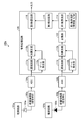
- FIG. 1 is a configuration diagram schematically illustrating the configuration of a light detection apparatus 100 according to the embodiment.
- the light detection device 100 includes power supply circuits 101a and 101b, an avalanche photodiode (APD) 102a sensitive to light, an avalanche photodiode (APD) 102b insensitive to light, and a front end.
- Amplifiers 103a and 103b, AD converters (ADC) 104a and 104b, and a signal processing circuit 105 are included.
- One or more avalanche photodiodes 102a and 102b are arranged in the avalanche photodiode array 102 described later.
- the power supply circuit 101a applies a voltage to the APD 102a so as to operate in the Geiger mode in which the reverse voltage is set to be equal to or higher than the breakdown voltage.
- the power supply circuit 101b applies a voltage to the APD 102b so as to operate in the Geiger mode in which the reverse voltage is set to be equal to or higher than the breakdown voltage.
- the power supply circuits 101a and 101b may be a common power supply.
- the APD 102a constitutes an APD pixel (pixel) that is sensitive to light that operates individually in the Geiger mode.
- the APD 102b constitutes an APD pixel (pixel) that is insensitive to light that operates individually in the Geiger mode.
- the APDs 102a and 102b are two-dimensionally arranged to constitute an avalanche photodiode array 102. That is, the APD 102a and the APD 102b are affected by the same environmental temperature.
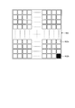
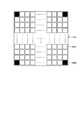
- FIG. 2 is a top view of the avalanche photodiode array 102 as seen from above.
- the avalanche photodiode array 102 outputs electric charges generated according to the number of photons of visible light received through a scintillator (not shown) (phosphor 130: see FIG. 9) as a current pulse through a quench resistor (not shown).
- the avalanche photodiode array 102 includes a plurality of (for example, about one hundred to several thousand) APDs 102a and one APD 102b. The position of the APD 102b in the avalanche photodiode array 102 may be arbitrarily set.
- the APD 102a outputs a current pulse corresponding to one photon when a visible photon is incident. All the APDs 102a are connected in parallel to each other. Therefore, the current pulses output from the respective APDs 102a are superimposed to form one current pulse.
- the avalanche photodiode array 102 has a current pulse having an area substantially proportional to the number of APDs 102a in which photons are incident (that is, the number corresponding to the number of visible photons incident). Output the number of received APDs 102a, that is, proportional to the total amount of charges generated) to the preamplifier 103a.
- the APD 102b is covered with a metal or the like so that visible light is not incident (for example, the incident side of the phosphor 130), and is configured to output a current pulse independently of the APD 102a.
- the avalanche photodiode generates a current pulse (that is, noise: thermal noise) by, for example, thermal excitation even when no photon is incident. Further, as described above, in the avalanche photodiode, the multiplication factor varies depending on the substrate temperature, the ambient temperature, and the like.
- a current pulse having a wave height corresponding to one photon that fluctuates according to the ambient temperature (or substrate temperature, etc.) has a high probability (10 5 to 10 6 ) with a certain probability. Is output to the preamplifier 103b.
- the preamplifier 103a multiplies the current pulse output from the APD 102a and outputs it to the ADC 104a as a voltage pulse.
- the preamplifier 103b multiplies the current pulse output from the APD 102b by N times and outputs it as a voltage pulse to the ADC 104b.
- M is set according to the number of APDs 102a.
- the value of N is, for example, 1 p. e. In order to enable AD conversion of the pulse, a value larger than the value of M is set.
- the ADC 104 a AD converts the voltage pulse output from the preamplifier 103 a and outputs the converted voltage value to the signal processing circuit 105.
- the signal processing circuit 105 includes gate generators 110a and 110b, delay circuits 111a and 111b, addition circuits 112a and 112b, a first holding circuit 113, a first division circuit 114, a second holding circuit 115, and a second division circuit 116. .
- the gate generator 110a receives the voltage value (AD value) output from the ADC 104a, forms a differential waveform from the voltage value, and generates a gate signal (gate) with an arbitrary threshold value.
- the gate signal is a signal used for measuring the voltage pulse, and is a signal for specifying the start and end of integration with respect to the voltage pulse.
- the gate generator 110b receives the voltage value (AD value) output from the ADC 104b, forms a differential waveform from the voltage value, and generates a gate signal (gate) with an arbitrary threshold value.
- the delay circuit 111a receives the voltage value (AD value) output from the ADC 104a, delays the voltage value so as to enable integration with respect to at least one voltage pulse, and outputs the delayed voltage value to the adder circuit 112a.
- the delay circuit 111b receives the voltage value (AD value) output from the ADC 104b, delays the voltage value so as to enable integration with respect to at least one voltage pulse, and outputs the delayed voltage value to the adder circuit 112b.
- the adder circuit 112a adds the voltage values received from the delay circuit 111a according to the gate signal generated by the gate generator 110a, and outputs the sum to the second divider circuit 116.
- the adder circuit 112b adds the voltage values received from the delay circuit 111b according to the gate signal generated by the gate generator 110b, and outputs the sum to the first divider circuit 114.
- the gate generator 110a, the delay circuit 111a, and the adder circuit 112a are integrated circuits that integrate one voltage pulse (current pulse having an area approximately proportional to the number of photons incident on the avalanche photodiode array 102) output from the ADC 104a. It has become.
- the gate generator 110b, the delay circuit 111b, and the adder circuit 112b are integrating circuits that integrate one voltage pulse (current pulse having an area corresponding to one photon) output from the ADC 104b.
- the first holding circuit 113 holds the holding value N / M and outputs the holding value to the first division circuit 114.
- N / M has the same number of bits as the ADCs 104a and 104b.
- the first division circuit 114 divides the current pulse of the area corresponding to one photon output from the addition circuit 112b by the holding value N / M, and outputs the result of the division to the second holding circuit 115.
- the result of division by the first division circuit 114 is obtained by multiplying the magnification of the current pulse output from the APD 102b by M.
- the second holding circuit 115 holds the result obtained by the division by the first division circuit 114 (division result) and outputs the result to the second division circuit 116.
- the second divider circuit 116 divides the voltage pulse output from the adder circuit 112a (a voltage pulse having a wave height substantially proportional to the number of photons incident on the avalanche photodiode array 102) by the division result received from the second holding circuit 115. Output. That is, the second division circuit 116 is incident on the avalanche photodiode array 102 by dividing the sum (integrated value) of the current pulses output from all the APDs 102a affected by the same environmental temperature by the current pulse output from the APD 102b. Calculate the number of photons emitted. Since the APD 102a and the APD 102b are affected by the same environmental temperature, the number of photons calculated by the second divider circuit 116 is constant regardless of the temperature.
- the photodetection device 100 is provided with a phosphor (not shown) in front of the avalanche photodiode array 102, and detects the number of photons generated by the phosphor according to the energy of radiation incident on the phosphor.
- the light detection device 100 is a radiation detection device that detects radiation.
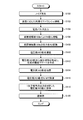
- FIG. 3 is a flowchart showing processing performed by the photodetection device 100 until the second holding circuit 115 holds a value corresponding to a voltage pulse (noise) output from the APD 102b without incident photons.
- step 100 the APD 102b generates noise (carrier that is a source of noise) with a certain probability by thermal excitation or the like.
- step 102 the APD 102b performs avalanche amplification (multiplication) with a gain corresponding to the temperature.
- step 104 the APD 102b outputs a current pulse corresponding to one photon.
- step 106 the preamplifier 103b amplifies the current pulse N times and converts it into a voltage pulse.
- step 108 the ADC 104b AD-converts the output of the preamplifier 103b and outputs the converted voltage value.
- step 110 the delay circuit 111b delays the voltage value (AD value) output from the ADC 104b.
- step 112 the gate generator 110b forms a differential waveform from the voltage value (AD value) output from the ADC 104b, and generates a gate with an arbitrary threshold value.
- step 114 the adding circuit 112b adds the voltage value (AD value) according to the gate generated by the gate generator 110b.
- step 116 the first division circuit 114 divides the voltage value (AD value) added by the addition circuit 112b by N / M.
- step 118 the first division circuit 114 converts the output corresponding to one photon from the APD 102b to a voltage value (AD value) multiplied by M as a result of the process of S116.
- step 120 the second holding circuit 115 holds the value converted by the first dividing circuit 114 as a voltage value (AD value) equivalent to one photon.
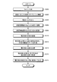
- FIG. 4 is a flowchart showing a process performed by the photodetecting device 100 in order to calculate the number of photons incident on the avalanche photodiode array 102.
- step 200 the avalanche photodiode array 102 receives visible light. That is, some of the APDs 102a are incident with photons (photons).
- step 202 the APD 102a that has entered the photon performs avalanche amplification (multiplication) with a gain according to temperature.
- step 204 the APD 102a that has entered the photon outputs a current pulse corresponding to one photon.
- step 206 the preamplifier 103a amplifies the current pulse superimposed by the output of each of the APDs 102a upon which the photons are incident, and converts it into a voltage pulse.
- step 208 the ADC 104a AD-converts the output of the preamplifier 103a and outputs the converted voltage value.
- step 210 the delay circuit 111a delays the voltage value (AD value) output from the ADC 104a.
- step 212 the gate generator 110a forms a differential waveform from the voltage value (AD value) output from the ADC 104a, and generates a gate with an arbitrary threshold value.
- step 214 the addition circuit 112a adds the voltage value (AD value) according to the gate generated by the gate generator 110a.
- step 216 the second dividing circuit 116 divides the voltage value (AD value) added by the adding circuit 112a by the voltage value (AD value) equivalent to one photon held by the second holding circuit 115.
- step 218 the second division circuit 116 regards (converts) the result (voltage value) divided by the processing in S216 as the number of photons.
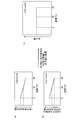
- FIG. 5 is a graph showing the effect of the operation of the light detection apparatus 100.
- FIG. 5 shows an example in which photons are incident on 100 APDs 102a among the APDs 102a included in the avalanche photodiode array 102. Further, it is assumed that the reverse voltage (Vop) applied to the APD 102a and the APD 102b is constant.
- FIG. 5A shows an AD value corresponding to one photon that changes in response to a temperature change (output of the adder circuit 112b).
- FIG. 5B shows an AD value (output of the adder circuit 112a) at the time of 100 photon incidence that changes according to a temperature change.
- the APD 102b is insensitive to light, but outputs a current pulse due to noise due to thermal excitation or the like. This current pulse can be regarded as equal to the current pulse output when one photon is incident on the APD 102a. Therefore, when the second divider circuit 116 divides the output of the adder circuit 112a by the output of the adder circuit 112b (after division by the first divider circuit 114), the photodetection device 100 calculates as shown in FIG. The number of photons is constant regardless of the temperature if the number of photons incident on the avalanche photodiode array 102 is the same.
- the photodetection device 100 divides the area of the current pulse output from all the APDs 102a affected by the same environmental temperature by the area of the current pulse corresponding to one photon output from the APD 102b.
- the number of photons incident on the avalanche photodiode array 102 can be calculated, and the temperature characteristics of the multiplication factor of the avalanche photodiode can be easily compensated.
- the photodetecting device 100 can easily compensate for the temperature characteristics of the multiplication factor of the avalanche photodiode even when there is no temperature sensor, temperature sensor driving circuit, bias voltage changing circuit, or the like. Furthermore, since the photodetection device 100 calculates the number of incident photons, even if a plurality of photons are used in parallel, there is no need to correct the variation between them. Further, the light detection device 100 does not need to perform correction for any change in temperature and change in power supply voltage.
- the photodetecting device 100 serves as a reference table (reference APD output value table) in which the output of the APD 102b that changes according to the environmental temperature is associated with each temperature (environmental temperature) and a voltage value equivalent to one photon is used as a reference. You may comprise so that it may memorize
- the signal processing circuit 105 includes a storage unit (not shown) and stores the reference table. The signal processing circuit 105 also saves (stores) the time-series data of the voltage value corresponding to the output of the APD 102a in the storage unit in association with the environmental temperature measured by the thermometer (not shown).
- the signal processing circuit 105 is configured as a correction unit that corrects and outputs the time-series data of the voltage value corresponding to the output of the APD 102a using the environmental temperature associated with the time-series data and the reference table. May be.
- FIG. 6 is a configuration diagram illustrating the configuration of a modified example (photodetection device 100a) of the photodetection device 100.
- FIG. 7 is a top view of the avalanche photodiode array 120 configured by two-dimensionally arranging the APDs 120a and 120b shown in FIG. 6 as viewed from above. 6 that are substantially the same as the components of the light detection apparatus 100 shown in FIG. 1 are denoted by the same reference numerals.
- the avalanche photodiode array 120 outputs a current pulse corresponding to the number of photons of visible light through a scintillator (phosphor 130: see FIG. 9) (not shown). As shown in FIG. 7, the avalanche photodiode array 120 includes a plurality (for example, about one hundred to several thousand) APDs 120a and a plurality (for example, four) APDs 102b. The position of the APD 120b in the avalanche photodiode array 120 may be arbitrarily set.
- the APD 120a constitutes an APD pixel (pixel) that is sensitive to light that operates individually in the Geiger mode.
- the APD 120b constitutes an APD pixel (pixel) that is insensitive to light that operates individually in the Geiger mode.
- the APD 120a and the APD 120b are affected by the same environmental temperature.
- the APD 120a outputs a current pulse corresponding to one photon when a visible photon is incident. All the APDs 120a are connected in parallel to each other. Accordingly, the current pulses output from each APD 120a are superimposed to form one current pulse.
- the avalanche photodiode array 120 has a current pulse having an area substantially proportional to the number of APDs 120a in which photons are incident (that is, corresponding to the number of incident photons of visible light). Output the number of received ADPs 102a, that is, proportional to the total amount of charges generated) to the preamplifier 103a.
- the APD 120b is covered with metal or the like so that visible light is not incident (for example, the incident side of the phosphor 130), and is configured to output a current pulse independently of the APD 120a. All the APDs 120b are connected to each other in parallel. Therefore, the current pulses output from each APD 120b are superimposed to form one current pulse. That is, the avalanche photodiode array 120 outputs a current pulse having an area substantially proportional to the number of APDs 120b that generated noise to the preamplifier 103b.
- the preamplifier 103b, the ADC 104b, the gate generator 110b, the delay circuit 111b, and the adder circuit 112b are the same as described with reference to FIG. 1 except that the input value is not always equivalent to one photon. Perform the action.
- the conversion unit 122 converts the voltage pulse output from the addition circuit 112b into a voltage pulse having a wave height equivalent to one photon, and outputs the voltage pulse to the first division circuit 114.
- the conversion unit 122 uses the fluctuation range in which the area of the current pulse output from the APD 102b can vary depending on the temperature, the area of the current pulse corresponding to one photon at the reference temperature, and the like. Determine the number of photons in the pulse (how many photons are equivalent). Then, the converter 122 calculates a voltage pulse having a wave height corresponding to one photon by dividing the voltage pulse output from the adder circuit 112b by the determined number of photons.
- the configuration having two or more pixels and the conversion unit is compared with the case where the number of voltage pulses having a wave height corresponding to one photon that can be measured per unit time is one pixel. That is, the calculation accuracy of a voltage pulse having a wave height equivalent to one photon is improved.
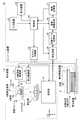
- FIG. 8 is a configuration diagram illustrating a configuration example of a radiation analysis apparatus having the light detection device 100.
- FIG. 9 is a schematic diagram schematically showing the position of the photodetecting device 100 in the radiation analyzer shown in FIG.
- the radiation analysis apparatus is an X-ray CT apparatus capable of performing photon counting CT. That is, the radiation analysis apparatus includes the light detection apparatus 100 and is an apparatus capable of reconstructing X-ray CT image data having a high S / N ratio by counting photons derived from X-rays transmitted through the subject by photon counting. is there.
- photon counting CT information on the energy component of X-rays can be obtained by measuring the energy value of photons.
- photon counting CT data collected by irradiating X-rays with one type of tube voltage can be divided into a plurality of energy components and imaged.
- the radiation analyzer includes a gantry device 10, a couch device 20, and a console device 30.
- the gantry device 10 is a device that irradiates the subject P with X-rays and counts the X-rays transmitted through the subject P, and includes an X-ray irradiation control unit 11, an X-ray generation device 12, and a detector 13 (light Including a detection device 100), a collection unit 14, a rotating frame 15, and a gantry drive unit 16.
- the rotating frame 15 supports the X-ray generator 12 and the detector 13 so as to face each other with the subject P interposed therebetween, and is rotated at a high speed in a circular orbit around the subject P by a gantry driving unit 16 described later.
- An annular frame An annular frame.
- the X-ray generator (radiation source) 12 is an apparatus that generates X-rays and irradiates the subject P with the generated X-rays, and includes an X-ray tube 12a, a wedge 12b, and a collimator 12c.
- the X-ray tube 12 a is a vacuum tube that irradiates the subject P with an X-ray beam by a high voltage supplied from an X-ray generation device 12 described later, and the X-ray beam is applied to the subject P as the rotating frame 15 rotates. Irradiate against.
- the X-ray tube 12a generates an X-ray beam that spreads with a fan angle and a cone angle.
- the wedge 12b is an X-ray filter for adjusting the X-ray dose of X-rays exposed from the X-ray tube 12a. Specifically, the wedge 12b transmits the X-rays exposed from the X-ray tube 12a so that the X-rays irradiated from the X-ray tube 12a to the subject P have a predetermined distribution. Attenuating filter.
- the wedge 12b is a filter obtained by processing aluminum so as to have a predetermined target angle and a predetermined thickness.
- the wedge is also called a wedge filter or a bow-tie filter.
- the radiation analysis apparatus includes a plurality of types of wedges 12b that can be switched according to imaging conditions.
- the X-ray irradiation control unit 11 to be described later switches the wedge 12b according to the imaging conditions.
- the X-ray generator 12 has two types of wedges.
- the collimator 12c is a slit for narrowing down the X-ray irradiation range in which the X-ray dose is adjusted by the wedge 12b under the control of the X-ray irradiation control unit 11 described later.
- the X-ray irradiation control unit 11 is a device that supplies a high voltage to the X-ray tube 12 a as a high voltage generation unit.
- the X-ray tube 12 a uses the high voltage supplied from the X-ray irradiation control unit 11 to perform X Generate a line.
- the X-ray irradiation control unit 11 adjusts the X-ray dose irradiated to the subject P by adjusting the tube voltage and tube current supplied to the X-ray tube 12a.
- the X-ray irradiation control unit 11 switches the wedge 12b.
- the X-ray irradiation control unit 11 adjusts the X-ray irradiation range (fan angle and cone angle) by adjusting the aperture of the collimator 12c.
- the radiation analyzer may be one in which an operator manually switches a plurality of types of wedges.
- the gantry driving unit 16 rotates the rotary frame 15 to rotate the X-ray generator 12 and the detector 13 on a circular orbit around the subject P.
- the detector 13 includes the light detection device 100 at the position shown in FIG. 9 and outputs a signal capable of measuring the energy value of the X-ray every time the X-ray enters.
- the photodetector 100 is configured such that the avalanche photodiode array 102 detects photons generated by X-rays incident on the phosphor 130.
- X-rays are, for example, X-rays irradiated from the X-ray tube 12a and transmitted through the subject P.
- the radiation analysis apparatus can measure the energy value of the radiation detected by the light detection apparatus 100 by performing arithmetic processing.
- the collecting unit 14 collects counting information that is a result of the counting process using the output signal of the detector 13. That is, the collection unit 14 discriminates individual signals output from the detector 13 and collects count information.
- the counting information is information collected from individual signals output from the detector 13 each time an X-ray irradiated from the X-ray tube 12a and transmitted through the subject P enters. Specifically, it is information in which a count value of X-rays incident on the detector 13 and an energy value are associated with each other.
- the collection unit 14 transmits the collected count information to the console device 30.
- the couch device 20 is a device on which the subject P is placed, and includes a couchtop 22 and a couch driving device 21.
- the couchtop 22 is a plate on which the subject P is placed, and the couch driving device 21 moves the couchtop 22 in the rotary frame 15 by moving the couchtop 22 in the Z-axis direction.
- the gantry device 10 executes, for example, a helical scan that rotates the rotating frame 15 while moving the top plate 22 to scan the subject P in a spiral shape.
- the gantry device 10 performs a conventional scan in which the subject P is scanned in a circular orbit by rotating the rotating frame 15 while the position of the subject P is fixed after the top plate 22 is moved.
- the gantry device 10 executes a step-and-shoot method in which the position of the top plate 22 is moved at regular intervals and a conventional scan is performed in a plurality of scan areas.
- the console device 30 is a device that accepts the operation of the radiation analyzer by the operator and reconstructs the X-ray CT image data using the count information collected by the gantry device 10.
- the console device 30 includes an input device 31, a display device 32, a scan control unit 33, a preprocessing unit 34, a projection data storage unit 35, an image reconstruction unit 36, an image storage unit 37, and a control unit 38. And have.
- the input device 31 includes a mouse, a keyboard, and the like that are used by the operator of the radiation analyzer to input various instructions and various settings, and transfers the instructions and setting information received from the operator to the control unit 38.
- the input device 31 receives imaging conditions for X-ray CT image data, reconstruction conditions for reconstructing X-ray CT image data, image processing conditions for X-ray CT image data, and the like from the operator.
- the display device 32 is a monitor that is referred to by the operator, displays X-ray CT image data to the operator under the control of the control unit 38, and provides various instructions and various information from the operator via the input device 31. Displays GUI (Graphical User Interface) for accepting settings.
- GUI Graphic User Interface
- the scan control unit 33 controls the operations of the X-ray irradiation control unit 11, the gantry driving unit 16, the collection unit 14, and the couch driving device 21 under the control of the control unit 38 to be described later, thereby counting in the gantry device 10. Controls the information collection process.
- the pre-processing unit 34 generates projection data by performing correction processing such as logarithmic conversion processing, offset correction, sensitivity correction, and beam hardening correction on the count information transmitted from the collection unit 14.
- correction processing such as logarithmic conversion processing, offset correction, sensitivity correction, and beam hardening correction
- the projection data storage unit 35 stores the projection data generated by the preprocessing unit 34. That is, the projection data storage unit 35 stores projection data (corrected count information) for reconstructing X-ray CT image data.
- projection data may be described as counting information.
- the image reconstruction unit 36 reconstructs X-ray CT image data using the projection data stored in the projection data storage unit 35.
- the reconstruction method there are various methods, for example, back projection processing. Further, as the back projection process, for example, a back projection process by an FBP (Filtered Back Projection) method can be mentioned. Further, the image reconstruction unit 36 generates image data by performing various kinds of image processing on the X-ray CT image data.
- the image reconstruction unit 36 stores the reconstructed X-ray CT image data and image data generated by various image processes in the image storage unit 37.
- the projection data generated from the counting information obtained by photon counting CT includes energy information of X-rays attenuated by passing through the subject P. Therefore, the image reconstruction unit 36 can reconstruct X-ray CT image data of a specific energy component, for example. In addition, the image reconstruction unit 36 can reconstruct X-ray CT image data of each of a plurality of energy components, for example.
- the image reconstruction unit 36 assigns a color tone corresponding to the energy component to each pixel of the X-ray CT image data of each energy component, and generates a plurality of X-ray CT image data color-coded according to the energy component, for example. Furthermore, image data in which the plurality of X-ray CT image data are superimposed can be generated.
- the image reconstruction unit 36 can generate image data that enables identification of the substance by using the K absorption edge unique to the substance. Before and after the K absorption edge, the X-ray attenuation coefficient differs greatly, and the count value also changes greatly.
- the image reconstruction unit 36 is a difference image obtained by subtracting the image data obtained by reconstructing the counting information of the energy region smaller than the K absorption edge from the image data obtained by reconstructing the counting information of the energy region larger than the K absorption edge.
- Generate data For example, the difference image data generated using the K absorption edge of the main component of the contrast agent is an image in which the region where the contrast agent is present is mainly depicted.
- Other image data generated by the image reconstruction unit 36 includes monochromatic X-ray image data, density image data, effective atomic number image data, and the like.
- the control unit 38 performs overall control of the radiation analyzer by controlling the operations of the gantry device 10, the couch device 20, and the console device 30. Specifically, the control unit 38 controls the CT scanning performed by the gantry device 10 by controlling the scan control unit 33. The control unit 38 also controls the image reconstruction process and the image generation process in the console device 30 by controlling the preprocessing unit 34 and the image reconstruction unit 36. The control unit 38 controls the display device 32 to display various image data stored in the image storage unit 37.
- the light detection device 100 supports the output of the APD 102a based on the environmental temperature. Correct the time-series data of the voltage value to be used.
- the image reconstruction unit 36 generates image data based on time-series data of voltage values corrected by the light detection device 100.
- the image reconstruction unit 36 generates two images (an image before correction and an image after correction) based on time-series data of voltage values before and after correction by the light detection device 100.
- the display device 32 may be configured to display two images.
- the light detection apparatus 100 is used in addition to the X-ray CT apparatus described above.
- the light detection apparatus 100 includes an X-ray diagnostic apparatus, a nuclear medicine imaging apparatus such as a PET (Positron Emission computed Tomography) apparatus and a SPECT (Single Photon Emission Computed Tomography) apparatus, and an X-ray CT apparatus and a nuclear medicine imaging apparatus. It is also used for the combined “PET-CT apparatus” and “SPECT-CT apparatus”.
- the light detection apparatus 100 may be used as a light receiving unit of a PET apparatus, and may constitute an apparatus combined with an MRI (magnetic resonance imaging apparatus).
Landscapes
- Health & Medical Sciences (AREA)
- Life Sciences & Earth Sciences (AREA)
- Engineering & Computer Science (AREA)
- Medical Informatics (AREA)
- Physics & Mathematics (AREA)
- Molecular Biology (AREA)
- High Energy & Nuclear Physics (AREA)
- Public Health (AREA)
- Heart & Thoracic Surgery (AREA)
- Optics & Photonics (AREA)
- Pathology (AREA)
- Radiology & Medical Imaging (AREA)
- Biomedical Technology (AREA)
- Biophysics (AREA)
- Veterinary Medicine (AREA)
- Surgery (AREA)
- Animal Behavior & Ethology (AREA)
- Nuclear Medicine, Radiotherapy & Molecular Imaging (AREA)
- General Health & Medical Sciences (AREA)
- Spectroscopy & Molecular Physics (AREA)
- General Physics & Mathematics (AREA)
- Pulmonology (AREA)
- Theoretical Computer Science (AREA)
- Computer Vision & Pattern Recognition (AREA)
- Mathematical Physics (AREA)
- Multimedia (AREA)
- Signal Processing (AREA)
- Measurement Of Radiation (AREA)
- Apparatus For Radiation Diagnosis (AREA)
- Nuclear Medicine (AREA)
- Light Receiving Elements (AREA)
Abstract
実施形態のフォトンカウンティングCT装置は、X線管と、シンチレータと、アバランシェフォトダイオードアレイと、保持部と、除算部と、画像生成部とを備える。X線管は、X線を発生する。シンチレータは、X線管より発生したX線を光に変換し放射する。アバランシェフォトダイオードアレイは、シンチレータの光の受光範囲である第1範囲内にあり、光に基づいて電気信号を出力するアバランシェフォトダイオードを具備する第1画素、及び第1範囲とは位置が異なる第2範囲内にあるアバランシェフォトダイオードを具備する第2画素からなる。除算部は、第1画素が出力する電気信号の積算値を、保持部が保持する電気信号の値で除算することにより、第1画素に入射した光の光子数を計数する。画像生成部は、計数された光の光子数に基づいて画像を再構成する。
Description
本発明の実施形態は、フォトンカウンティングCT装置、光検出装置、放射線検出装置及び放射線分析装置に関する。
光検出装置の一つとして、アバランシェフォトダイオードアレイを用いた光検出装置が知られている。この光検出装置は、単一光子レベルで光検出が可能であるという特徴を有する。また、この光検出装置は、アバランシェフォトダイオードの増倍率が基板温度及び周囲温度により変動するという問題がある。この問題を回避するために、温度に応じてアバランシェフォトダイオードに印加する逆電圧を変化させることは公知である。
しかしながら、温度に応じてアバランシェフォトダイオードに印加する逆電圧を変化させるためには、温度センサ、温度センサ駆動回路及びバイアス電圧変更回路などが必要となり、構成が複雑になってしまうという問題があった。本発明が解決しようとする課題は、アバランシェフォトダイオードの増倍率の温度特性を容易に補償することができるフォトンカウンティングCT装置、光検出装置、放射線検出装置及び放射線分析装置を提供することである。
実施形態のフォトンカウンティングCT装置は、X線管と、シンチレータと、アバランシェフォトダイオードアレイと、保持部と、除算部と、画像生成部とを備える。X線管は、X線を発生する。シンチレータは、X線管より発生したX線を光に変換し放射する。アバランシェフォトダイオードアレイは、シンチレータの光の受光範囲である第1範囲内にあり、光に基づいて電気信号を出力するアバランシェフォトダイオードを具備する第1画素、及び第1範囲とは位置が異なる第2範囲内にあるアバランシェフォトダイオードを具備する第2画素からなる。保持部は、第2画素が出力する電気信号の値を保持する。除算部は、第1画素が出力する電気信号の積算値を、保持部が保持する電気信号の値で除算することにより、第1画素に入射した光の光子数を計数する。画像生成部は、計数された光の光子数に基づいて画像を再構成する。
以下に添付図面を参照して、実施形態にかかる光検出装置100について説明する。
(実施形態)
図1は、実施形態にかかる光検出装置100の構成を模式的に例示する構成図である。図1に示すように、光検出装置100は、電源回路101a,101b、光に対して有感なアバランシェフォトダイオード(APD)102a、光に対して不感なアバランシェフォトダイオード(APD)102b、前置増幅器103a,103b、AD変換器(ADC)104a,104b及び信号処理回路105を有する。なお、アバランシェフォトダイオード102a,102bは、後述するアバランシェフォトダイオードアレイ102においてそれぞれ1つ以上配列されるものである。
図1は、実施形態にかかる光検出装置100の構成を模式的に例示する構成図である。図1に示すように、光検出装置100は、電源回路101a,101b、光に対して有感なアバランシェフォトダイオード(APD)102a、光に対して不感なアバランシェフォトダイオード(APD)102b、前置増幅器103a,103b、AD変換器(ADC)104a,104b及び信号処理回路105を有する。なお、アバランシェフォトダイオード102a,102bは、後述するアバランシェフォトダイオードアレイ102においてそれぞれ1つ以上配列されるものである。
電源回路101aは、APD102aに対し、逆電圧を降伏電圧以上に設定したガイガーモードで動作するように電圧を印加する。電源回路101bは、APD102bに対し、逆電圧を降伏電圧以上に設定したガイガーモードで動作するように電圧を印加する。電源回路101a,101bは、共通の電源とされてもよい。
APD102aは、ガイガーモードで個別に動作する光に対して有感なAPDピクセル(画素)を構成する。APD102bは、ガイガーモードで個別に動作する光に対して不感なAPDピクセル(画素)を構成する。そして、APD102a,102bは、2次元に配列されてアバランシェフォトダイオードアレイ102を構成している。つまり、APD102a及びAPD102bは、それぞれ同じ環境温度の影響を受ける。
図2は、アバランシェフォトダイオードアレイ102を上面から見た上面図である。アバランシェフォトダイオードアレイ102は、図示しないシンチレータ(蛍光体130:図9参照)を介して受光した可視光の光子数に応じて発生した電荷を、図示しないクエンチ抵抗を介して電流パルスとして出力する。図2に示すように、アバランシェフォトダイオードアレイ102は、複数(例えば約百~数千個)のAPD102aと、1つのAPD102bとを有する。アバランシェフォトダイオードアレイ102におけるAPD102bの位置は任意に設定されてよい。
APD102aは、可視光の光子が入射されると、1光子相当の電流パルスを出力する。全てのAPD102aは、互いに並列接続されている。従って、各APD102aがそれぞれ出力した電流パルスは、重畳されて1つの電流パルスとなる。つまり、アバランシェフォトダイオードアレイ102は、光子が入射されたAPD102aの数(即ち入射される可視光の光子数に相当するものとする)にほぼ比例する面積の電流パルス(電流パルスの時間方向に対する面積は受光したAPD102aの数、すなわち発生した総電荷量に比例する)を前置増幅器103aに対して出力する。
APD102bは、可視光が入射されないように(例えば蛍光体130の入射側が)金属などで覆われおり、APD102aとは独立して電流パルスを出力するように構成されている。アバランシェフォトダイオードは、光子が入射されなくても、例えば熱励起によって電流パルス(即ちノイズ:熱雑音)を発生させる。また、上述したように、アバランシェフォトダイオードは、増倍率が基板温度及び周囲温度などによって変動する。つまり、APD102bは、ガイガーモードにされているため、周囲の温度(又は基板の温度など)に応じて変動した1光子相当の波高の電流パルスをある確率で高い増倍率(105~106)によって前置増幅器103bに対して出力する。
前置増幅器103aは、APD102aが出力した電流パルスをM倍にし、電圧パルスとしてADC104aに対して出力する。前置増幅器103bは、APD102bが出力した電流パルスをN倍にし、電圧パルスとしてADC104bに対して出力する。なお、Mの値は、APD102aの数に応じて設定される。また、Nの値は、例えば1p.e.パルスをAD変換可能にするために、Mの値よりも大きな値に設定されている。
ADC104aは、前置増幅器103aが出力した電圧パルスをAD変換し、変換した電圧値を信号処理回路105に対して出力する。ADC104bは、前置増幅器103bが出力した電圧パルスをAD変換し、変換した電圧値を信号処理回路105に対して出力する。
信号処理回路105は、ゲート発生器110a,110b、遅延回路111a,111b、加算回路112a,112b、第1保持回路113、第1除算回路114、第2保持回路115及び第2除算回路116を有する。
ゲート発生器110aは、ADC104aが出力した電圧値(AD値)を受入れ、電圧値から微分波形を形成し、任意の閾値でゲート信号(ゲート)を生成する。ゲート信号は、電圧パルスを測定するために用いる信号であり、電圧パルスに対する積分開始と終了を特定する信号である。ゲート発生器110bは、ADC104bが出力した電圧値(AD値)を受入れ、電圧値から微分波形を形成し、任意の閾値でゲート信号(ゲート)を生成する。
遅延回路111aは、ADC104aが出力した電圧値(AD値)を受入れ、少なくとも1つの電圧パルスに対する積分を可能にするように、電圧値を遅延させて加算回路112aに対して出力する。遅延回路111bは、ADC104bが出力した電圧値(AD値)を受入れ、少なくとも1つの電圧パルスに対する積分を可能にするように、電圧値を遅延させて加算回路112bに対して出力する。
加算回路112aは、ゲート発生器110aが生成したゲート信号に応じて、遅延回路111aから受入れた電圧値を加算し、第2除算回路116に対して出力する。加算回路112bは、ゲート発生器110bが生成したゲート信号に応じて、遅延回路111bから受入れた電圧値を加算し、第1除算回路114に対して出力する。
つまり、ゲート発生器110a、遅延回路111a及び加算回路112aは、ADC104aが出力した1つの電圧パルス(アバランシェフォトダイオードアレイ102に入射された光子数にほぼ比例する面積の電流パルス)を積分する積分回路となっている。
ゲート発生器110b、遅延回路111b及び加算回路112bは、ADC104bが出力した1つの電圧パルス(1光子相当の面積の電流パルス)を積分する積分回路となっている。
第1保持回路113は、保持値N/Mを保持し、第1除算回路114に対して保持値を出力する。N/Mは、ADC104a,104bと同じビット数の値にされている。
第1除算回路114は、加算回路112bが出力した1光子相当の面積の電流パルスを保持値N/Mで除算し、除算した結果を第2保持回路115に対して出力する。第1除算回路114が除算した結果は、APD102bが出力した電流パルスの倍率をM倍にしたものとなる。
第2保持回路115は、第1除算回路114が除算した結果(除算結果)を保持し、第2除算回路116に対して出力する。
第2除算回路116は、加算回路112aが出力した電圧パルス(アバランシェフォトダイオードアレイ102に入射された光子数にほぼ比例する波高の電圧パルス)を第2保持回路115から受入れた除算結果で除算して出力する。つまり、第2除算回路116は、同じ環境温度の影響を受けた全APD102aが出力する電流パルスの総和(積算値)をAPD102bが出力する電流パルスで除算することにより、アバランシェフォトダイオードアレイ102に入射された光子数を算出する。APD102a及びAPD102bは、それぞれ同じ環境温度の影響を受けているので、第2除算回路116が算出した光子数は、温度によらず一定となる。
なお、光検出装置100は、アバランシェフォトダイオードアレイ102の前段に図示しない蛍光体が設けられ、蛍光体に入射される放射線のエネルギーに応じて蛍光体が発生させた光子数を検出する。光検出装置100は、放射線を検出する放射線検出装置である。
次に、光検出装置100の動作について説明する。図3は、APD102bが光子を入射されることなく出力した電圧パルス(ノイズ)に相当する値を第2保持回路115に保持するまでに光検出装置100が行う処理を示すフローチャートである。
図3に示すように、ステップ100(S100)において、APD102bは、熱励起などによってある確率でノイズ(ノイズの源となるキャリア)を発生させる。
ステップ102(S102)において、APD102bは、温度に応じた利得でアバランシェ増幅(増倍)を行う。
ステップ104(S104)において、APD102bは、1光子相当の電流パルスを出力する。
ステップ106(S106)において、前置増幅器103bは、電流パルスをN倍に増幅し、電圧パルスに変換する。
ステップ108(S108)において、ADC104bは、前置増幅器103bの出力をAD変換し、変換した電圧値を出力する。
ステップ110(S110)において、遅延回路111bは、ADC104bが出力した電圧値(AD値)を遅延させる。
ステップ112(S112)において、ゲート発生器110bは、ADC104bが出力した電圧値(AD値)から微分波形を形成し、任意の閾値でゲートを生成する。
ステップ114(S114)において、加算回路112bは、ゲート発生器110bが生成したゲートに応じて電圧値(AD値)を加算する。
ステップ116(S116)において、第1除算回路114は、加算回路112bが加算した電圧値(AD値)をN/Mで除算する。
ステップ118(S118)において、第1除算回路114は、S116の処理による結果として、APD102bによる1光子相当の出力をM倍した電圧値(AD値)に換算する。
ステップ120(S120)において、第2保持回路115は、第1除算回路114が換算した値を1光子相当の電圧値(AD値)として保持する。
図4は、アバランシェフォトダイオードアレイ102に入射された光子数を算出するために光検出装置100が行う処理を示すフローチャートである。
図4に示すように、ステップ200(S200)において、アバランシェフォトダイオードアレイ102は、可視光を入射される。つまり、APD102aのいくつかは、光子(フォトン)を入射される。
ステップ202(S202)において、光子を入射されたAPD102aは、温度に応じた利得でアバランシェ増幅(増倍)を行う。
ステップ204(S204)において、光子を入射されたAPD102aは、1光子相当の電流パルスを出力する。
ステップ206(S206)において、前置増幅器103aは、光子を入射されたAPD102aそれぞれが出力して重畳された電流パルスをM倍に増幅し、電圧パルスに変換する。
ステップ208(S208)において、ADC104aは、前置増幅器103aの出力をAD変換し、変換した電圧値を出力する。
ステップ210(S210)において、遅延回路111aは、ADC104aが出力した電圧値(AD値)を遅延させる。
ステップ212(S212)において、ゲート発生器110aは、ADC104aが出力した電圧値(AD値)から微分波形を形成し、任意の閾値でゲートを生成する。
ステップ214(S214)において、加算回路112aは、ゲート発生器110aが生成したゲートに応じて電圧値(AD値)を加算する。
ステップ216(S216)において、第2除算回路116は、加算回路112aが加算した電圧値(AD値)を、第2保持回路115が保持した1光子相当の電圧値(AD値)で除算する。
ステップ218(S218)において、第2除算回路116は、S216の処理で除算した結果(電圧値)を光子数とみなして(変換して)出力する。
図5は、光検出装置100の動作による効果を示すグラフである。なお、図5においては、アバランシェフォトダイオードアレイ102が有するAPD102aのうち、100個のAPD102aに光子が入射された場合が例に示されている。また、APD102a,APD102bに印加される逆電圧(Vop)は一定であるとする。図5(a)においては、温度変化に応じて変化する1光子相当のAD値(加算回路112bの出力)が示されている。図5(b)においては、温度変化に応じて変化する100光子入射時のAD値(加算回路112aの出力)が示されている。
APD102bは光に対して不感であるが、熱励起等によるノイズによって電流パルスを出力する。この電流パルスを、APD102aに1光子入射したときに出力される電流パルスと等しいとみなすことができる。従って、第2除算回路116が加算回路112aの出力を加算回路112bの出力(第1除算回路114による除算後)で除算すると、図5(c)に示すように、光検出装置100が算出する光子数は、アバランシェフォトダイオードアレイ102に入射される光子数が同じであれば温度によらず一定となる。
このように、光検出装置100は、同じ環境温度の影響を受けた全APD102aが出力する電流パルスの面積をAPD102bが出力する1光子相当の電流パルスの面積で除算するので、環境温度によらずアバランシェフォトダイオードアレイ102に入射された光子数を算出することができ、アバランシェフォトダイオードの増倍率の温度特性を容易に補償することができる。
つまり、光検出装置100は、温度センサ、温度センサ駆動回路及びバイアス電圧変更回路などがない場合にも、アバランシェフォトダイオードの増倍率の温度特性を容易に補償することができる。さらに、光検出装置100は、入射される光子数を算出するので、複数個が並列されて用いられても、相互間のばらつきを補正する必要がない。また、光検出装置100は、温度変化及び電源電圧変化のいずれに対しても、補正を行う必要がない。
また、光検出装置100は、環境温度に応じて変化するAPD102bの出力を、温度(環境温度)毎に対応付けて1光子相当の電圧値の基準にする基準テーブル(基準APD出力値テーブル)として予め記憶しておくように構成されてもよい。例えば、信号処理回路105が図示しない記憶部を備えて基準テーブルを記憶する。そして、信号処理回路105は、APD102aの出力に対応する電圧値の時系列データも、温度計(図示せず)が計測した環境温度を対応付けて記憶部に保存(記憶)する。この場合、信号処理回路105は、時系列データに対応付けられた環境温度と、基準テーブルとを用いて、APD102aの出力に対応する電圧値の時系列データを補正して出力する補正部として構成されてもよい。
(変形例)
図6は、光検出装置100の変形例(光検出装置100a)の構成を例示する構成図である。図7は、図6に示したAPD120a,120bが2次元に配列されて構成されるアバランシェフォトダイオードアレイ120を上面から見た上面図である。なお、図6に示した光検出装置100aの構成部分のうち、図1に示した光検出装置100の構成要素と実質的に同じものには、同一の符号が付してある。
図6は、光検出装置100の変形例(光検出装置100a)の構成を例示する構成図である。図7は、図6に示したAPD120a,120bが2次元に配列されて構成されるアバランシェフォトダイオードアレイ120を上面から見た上面図である。なお、図6に示した光検出装置100aの構成部分のうち、図1に示した光検出装置100の構成要素と実質的に同じものには、同一の符号が付してある。
アバランシェフォトダイオードアレイ120は、図示しないシンチレータ(蛍光体130:図9参照)を介して可視光の光子数に応じた電流パルスを出力する。図7に示すように、アバランシェフォトダイオードアレイ120は、複数(例えば約百~数千個)のAPD120aと、複数(例えば4つ)のAPD102bとを有する。アバランシェフォトダイオードアレイ120におけるAPD120bの位置は任意に設定されてよい。
APD120aは、ガイガーモードで個別に動作する光に対して有感なAPDピクセル(画素)を構成する。APD120bは、ガイガーモードで個別に動作する光に対して不感なAPDピクセル(画素)を構成する。APD120a及びAPD120bは、それぞれ同じ環境温度の影響を受ける。
APD120aは、可視光の光子が入射されると、1光子相当の電流パルスを出力する。全てのAPD120aは、互いに並列接続されている。従って、各APD120aがそれぞれ出力した電流パルスは、重畳されて1つの電流パルスとなる。つまり、アバランシェフォトダイオードアレイ120は、光子が入射されたAPD120aの数(即ち入射される可視光の光子数に相当するものとする)にほぼ比例する面積の電流パルス(電流パルスの時間方向に対する面積は受光したADP102aの数、すなわち発生した総電荷量に比例する)を前置増幅器103aに対して出力する。
APD120bは、可視光が入射されないように(例えば蛍光体130の入射側が)金属などで覆われおり、APD120aとは独立して電流パルスを出力するように構成されている。全てのAPD120bは、互いに並列接続されている。従って、各APD120bがそれぞれ出力した電流パルスは、重畳されて1つの電流パルスとなる。つまり、アバランシェフォトダイオードアレイ120は、ノイズを発生させたAPD120bの数にほぼ比例する面積の電流パルスを前置増幅器103bに対して出力する。
前置増幅器103b、ADC104b、ゲート発生器110b、遅延回路111b、加算回路112bは、入力される値が1光子相当であるとは限らない点を除いて、図1を用いて説明した動作と同じ動作を行う。
変換部122は、加算回路112bが出力した電圧パルスを1光子相当の波高の電圧パルスに変換し、第1除算回路114に対して出力する。例えば、変換部122は、APD102bが出力する電流パルスの面積が温度に応じて変動し得る変動幅、及び基準温度における1光子相当の電流パルスの面積などを用いて、加算回路112bが出力した電圧パルスの光子数(何光子相当であるか)を判定する。そして、変換部122は、加算回路112bが出力した電圧パルスを判定した光子数で除算することにより、1光子相当の波高の電圧パルスを算出する。2以上の画素と変換部を有する構成は、単位時間あたりに計測できる1光子相当の波高の電圧パルスの数が、1つの画素を有する場合に比べておおくなる。すなわち、1光子相当の波高の電圧パルスの計算精度が良くなる。
(実施例)
次に、放射線検出装置でもある光検出装置100を有する放射線分析装置について説明する。図8は、光検出装置100を有する放射線分析装置の構成例を示す構成図である。図9は、図8に示した放射線分析装置における光検出装置100の位置を模式的に示した模式図である。放射線分析装置は、フォトンカウンティングCTを実行可能なX線CT装置である。すなわち、放射線分析装置は、光検出装置100を備え、フォトンカウンティングによって被検体を透過したX線に由来する光子も計数することにより、SN比の高いX線CT画像データを再構成可能な装置である。
次に、放射線検出装置でもある光検出装置100を有する放射線分析装置について説明する。図8は、光検出装置100を有する放射線分析装置の構成例を示す構成図である。図9は、図8に示した放射線分析装置における光検出装置100の位置を模式的に示した模式図である。放射線分析装置は、フォトンカウンティングCTを実行可能なX線CT装置である。すなわち、放射線分析装置は、光検出装置100を備え、フォトンカウンティングによって被検体を透過したX線に由来する光子も計数することにより、SN比の高いX線CT画像データを再構成可能な装置である。
個々の光子は、異なるエネルギーを有する。フォトンカウンティングCTでは、光子のエネルギー値の計測を行なうことにより、X線のエネルギー成分の情報を得ることができる。フォトンカウンティングCTでは、1種類の管電圧でX線を照射することで収集されたデータを複数のエネルギー成分に分けて画像化することができる。
図8に示すように、放射線分析装置は、架台装置10と、寝台装置20と、コンソール装置30とを有する。
架台装置10は、被検体PにX線を照射し、被検体Pを透過したX線を計数する装置であり、X線照射制御部11と、X線発生装置12と、検出器13(光検出装置100を含む)と、収集部14と、回転フレーム15と、架台駆動部16とを有する。
回転フレーム15は、X線発生装置12と検出器13とを被検体Pを挟んで対向するように支持し、後述する架台駆動部16によって被検体Pを中心した円軌道にて高速に回転する円環状のフレームである。
X線発生装置(放射線源)12は、X線を発生し、発生したX線を被検体Pへ照射する装置であり、X線管12aと、ウェッジ12bと、コリメータ12cとを有する。
X線管12aは、後述するX線発生装置12により供給される高電圧により被検体PにX線ビームを照射する真空管であり、回転フレーム15の回転にともなって、X線ビームを被検体Pに対して照射する。X線管12aは、ファン角及びコーン角を持って広がるX線ビームを発生する。
ウェッジ12bは、X線管12aから曝射されたX線のX線量を調節するためのX線フィルタである。具体的には、ウェッジ12bは、X線管12aから被検体Pへ照射されるX線が、予め定められた分布になるように、X線管12aから曝射されたX線を透過して減衰するフィルタである。
例えば、ウェッジ12bは、所定のターゲット角度や所定の厚みとなるようにアルミニウムを加工したフィルタである。なお、ウェッジは、ウェッジフィルター(wedge filter)や、ボウタイフィルター(bow-tie filter)とも呼ばれる。また、放射線分析装置は、撮影条件に応じて切り替えられる複数種類のウェッジ12bを有する。例えば、後述するX線照射制御部11は、撮影条件に応じてウェッジ12bを切り替える。例えば、X線発生装置12は、2種類のウェッジを有する。
コリメータ12cは、後述するX線照射制御部11の制御により、ウェッジ12bによってX線量が調節されたX線の照射範囲を絞り込むためのスリットである。
X線照射制御部11は、高電圧発生部として、X線管12aに高電圧を供給する装置であり、X線管12aは、X線照射制御部11から供給される高電圧を用いてX線を発生する。X線照射制御部11は、X線管12aに供給する管電圧や管電流を調整することで、被検体Pに対して照射されるX線量を調整する。
また、X線照射制御部11は、ウェッジ12bの切り替えを行なう。また、X線照射制御部11は、コリメータ12cの開口度を調整することにより、X線の照射範囲(ファン角やコーン角)を調整する。なお、放射線分析装置は、複数種類のウェッジを、操作者が手動で切り替えるものであってもよい。
架台駆動部16は、回転フレーム15を回転駆動させることによって、被検体Pを中心とした円軌道上でX線発生装置12と検出器13とを旋回させる。
検出器13は、図9に示した位置に光検出装置100を備え、X線が入射するごとに、当該X線のエネルギー値を計測可能な信号を出力する。光検出装置100は、蛍光体130に入射されたX線により発生した光子をアバランシェフォトダイオードアレイ102が検出する構成となっている。X線は、例えば、X線管12aから照射され被検体Pを透過したX線である。放射線分析装置は、演算処理を行なうことで、光検出装置100が検出した放射線のエネルギー値を計測することができる。
収集部14(図8)は、検出器13の出力信号を用いた計数処理の結果である計数情報を収集する。すなわち、収集部14は、検出器13から出力される個々の信号を弁別して、計数情報を収集する。計数情報は、X線管12aから照射され被検体Pを透過したX線が入射するごとに検出器13が出力した個々の信号から収集される情報である。具体的には、検出器13に入射したX線の計数値とエネルギー値とが対応付けられた情報である。収集部14は、収集した計数情報を、コンソール装置30に送信する。
寝台装置20は、被検体Pを載せる装置であり、天板22と、寝台駆動装置21とを有する。天板22は、被検体Pが載置される板であり、寝台駆動装置21は、天板22をZ軸方向へ移動して、被検体Pを回転フレーム15内に移動させる。
なお、架台装置10は、例えば、天板22を移動させながら回転フレーム15を回転させて被検体Pをらせん状にスキャンするヘリカルスキャンを実行する。または、架台装置10は、天板22を移動させた後に被検体Pの位置を固定したままで回転フレーム15を回転させて被検体Pを円軌道にてスキャンするコンベンショナルスキャンを実行する。または、架台装置10は、天板22の位置を一定間隔で移動させてコンベンショナルスキャンを複数のスキャンエリアで行なうステップアンドシュート方式を実行する。
コンソール装置30は、操作者による放射線分析装置の操作を受け付けるとともに、架台装置10によって収集された計数情報を用いてX線CT画像データを再構成する装置である。コンソール装置30は、入力装置31と、表示装置32と、スキャン制御部33と、前処理部34と、投影データ記憶部35と、画像再構成部36と、画像記憶部37と、制御部38とを有する。
入力装置31は、放射線分析装置の操作者が各種指示や各種設定の入力に用いるマウスやキーボード等を有し、操作者から受け付けた指示や設定の情報を、制御部38に転送する。例えば、入力装置31は、操作者から、X線CT画像データの撮影条件や、X線CT画像データを再構成する際の再構成条件や、X線CT画像データに対する画像処理条件等を受け付ける。
表示装置32は、操作者によって参照されるモニタであり、制御部38による制御のもと、X線CT画像データを操作者に表示したり、入力装置31を介して操作者から各種指示や各種設定等を受け付けるためのGUI(Graphical User Interface)を表示したりする。
スキャン制御部33は、後述する制御部38の制御のもと、X線照射制御部11、架台駆動部16、収集部14及び寝台駆動装置21の動作を制御することで、架台装置10における計数情報の収集処理を制御する。
前処理部34は、収集部14から送信された計数情報に対して、対数変換処理、オフセット補正、感度補正、ビームハードニング補正等の補正処理を行なうことで、投影データを生成する。
投影データ記憶部35は、前処理部34により生成された投影データを記憶する。すなわち、投影データ記憶部35は、X線CT画像データを再構成するための投影データ(補正済み計数情報)を記憶する。なお、以下では、投影データを計数情報として記載する場合がある。
画像再構成部36は、投影データ記憶部35が記憶する投影データを用いてX線CT画像データを再構成する。再構成方法としては、種々の方法があり、例えば、逆投影処理が挙げられる。また、逆投影処理としては、例えば、FBP(Filtered Back Projection)法による逆投影処理が挙げられる。また、画像再構成部36は、X線CT画像データに対して各種画像処理を行なうことで、画像データを生成する。画像再構成部36は、再構成したX線CT画像データや、各種画像処理により生成した画像データを画像記憶部37に格納する。
ここで、フォトンカウンティングCTで得られる計数情報から生成された投影データには、被検体Pを透過することで減弱されたX線のエネルギー情報が含まれている。このため、画像再構成部36は、例えば、特定のエネルギー成分のX線CT画像データを再構成することができる。また、画像再構成部36は、例えば、複数のエネルギー成分それぞれのX線CT画像データを再構成することができる。
また、画像再構成部36は、例えば、各エネルギー成分のX線CT画像データの各画素にエネルギー成分に応じた色調を割り当て、エネルギー成分に応じて色分けされた複数のX線CT画像データを生成することができ、更に、これら複数のX線CT画像データを重畳した画像データを生成することができる。
また、画像再構成部36は、物質固有のK吸収端を利用して、当該物質の同定が可能となる画像データを生成することができる。K吸収端の前後では、X線の減弱係数が大きく異なるため、計数値も大きく変化する。例えば、画像再構成部36は、K吸収端より小さいエネルギー領域の計数情報を再構成した画像データと、当該K吸収端より大きいエネルギー領域の計数情報を再構成した画像データとを差分した差分画像データを生成する。例えば、造影剤の主成分のK吸収端を用いて生成された差分画像データは、当該造影剤が存在する領域が主に描出された画像となる。また、画像再構成部36が生成する他の画像データとしては、単色X線画像データや密度画像データ、実効原子番号画像データ等が挙げられる。
制御部38は、架台装置10、寝台装置20及びコンソール装置30の動作を制御することによって、放射線分析装置の全体制御を行う。具体的には、制御部38は、スキャン制御部33を制御することで、架台装置10で行なわれるCTスキャンを制御する。また、制御部38は、前処理部34や、画像再構成部36を制御することで、コンソール装置30における画像再構成処理や画像生成処理を制御する。また、制御部38は、画像記憶部37が記憶する各種画像データを、表示装置32に表示するように制御する。
また、上述した基準テーブルと、APD102aの出力に対応する電圧値の時系列データとを信号処理回路105が記憶している場合、光検出装置100は、環境温度に基づいて、APD102aの出力に対応する電圧値の時系列データを補正する。この場合、例えば画像再構成部36は、光検出装置100が補正した電圧値の時系列データに基づいて、画像データを生成する。さらに、コンソール装置30は、光検出装置100が補正する前後それぞれの電圧値の時系列データに基づく2つの画像(補正前画像及び補正後画像)を画像再構成部36が生成し、生成された2つの画像を表示装置32が表示するように構成されてもよい。
なお、光検出装置100は、上述したX線CT装置以外にも用いられる。例えば、光検出装置100は、X線診断装置、PET(Positron Emission computed Tomography)装置及びSPECT(Single Photon Emission Computed Tomography)装置等の核医学イメージング装置、並びにX線CT装置と核医学イメージング装置とを組み合わせた「PET-CT装置」及び「SPECT-CT装置」等にも用いられる。また、光検出装置100は、PET装置の受光部として用いられ、MRI(磁気共鳴画像装置)が組み合わされた装置を構成してもよい。
また、本発明のいくつかの実施形態を複数の組み合わせによって説明したが、これらの実施形態は例として提示したものであり、発明の範囲を限定することは意図していない。これら新規の実施形態は、その他の様々な形態で実施されることが可能であり、発明の要旨を逸脱しない範囲で、種々の省略、置き換え、変更を行うことができる。これら実施形態やその変形は、発明の範囲や要旨に含まれるとともに、請求の範囲に記載された発明とその均等の範囲に含まれる。
Claims (8)
- X線を発生するX線管と、
前記X線管より発生したX線を光に変換し放射するシンチレータと、
前記シンチレータの光の受光範囲である第1範囲内にあり、前記光に基づいて電気信号を出力するアバランシェフォトダイオードを具備する第1画素、及び前記第1範囲とは位置が異なる第2範囲内にあるアバランシェフォトダイオードを具備する第2画素からなるアバランシェフォトダイオードアレイと、
前記第2画素が出力する電気信号の値を保持する保持部と、
前記第1画素が出力する電気信号の積算値を、前記保持部が保持する電気信号の値で除算することにより、前記第1画素に入射した光の光子数を計数する除算部と、
前記計数された光の光子数に基づいて画像を再構成する画像生成部と
を備えるフォトンカウンティングCT装置。 - 前記保持部が保持する電気信号の値は、
前記第2画素にあるアバランシェフォトダイオードの熱雑音による出力値である
請求項1記載のフォトンカウンティングCT装置。 - 前記アバランシェフォトダイオードアレイは、
複数の前記第2画素を有し、
複数の前記第2画素が出力する電気信号の積算値から、1つの前記第2画素が出力する電気信号の値を得る変換部をさらに有し、
前記保持部は、前記変換部が得た電気信号の値を保持する
請求項1または2に記載のフォトンカウンティングCT装置。 - 前記第1画素及び前記第2画素が具備するアバランシェフォトダイオードは、
ガイガーモードで動作する請求項1乃至3のいずれか1項に記載のフォトンカウンティングCT装置。 - 前記第2画素が具備するアバランシェフォトダイオードの出力を温度毎に予め対応付けた基準テーブルと、前記第1画素が具備するアバランシェフォトダイオードの出力と温度とを対応付けた時系列データを記憶する記憶部と、
前記記憶部が記憶する前記基準テーブル及び前記時系列データに基づいて、前記時系列データを補正する補正部と、
をさらに有し、
前記画像生成部は、
前記補正部が補正した前記時系列データに基づく画像を生成する請求項1乃至4のいずれか1項に記載のフォトンカウンティングCT装置。 - 光の受光範囲である第1範囲内にあり、前記光に基づいて電気信号を出力するアバランシェフォトダイオードを具備する第1画素、及び前記第1範囲とは位置が異なる第2範囲内にあるアバランシェフォトダイオードを具備する第2画素からなるアバランシェフォトダイオードアレイと、
前記第2画素が出力する電気信号の値を保持する保持部と、
前記第1画素が出力する電気信号の積算値を、前記保持部が保持する電気信号の値で除算することにより、前記第1画素に入射した光の光子数を計数する除算部と、
を有する光検出装置。 - 放射線が入射されることにより、放射線のエネルギーに応じて光子を発生させる蛍光体と、
前記蛍光体が発生させた光子数を算出する請求項6に記載の光検出装置と、
を有する放射線検出装置。 - 前記蛍光体へX線を放射する放射線源を更に有し、
前記放射線源が放射した放射線に起因する光子数を算出する
請求項7に記載の放射線分析装置。
Priority Applications (1)
| Application Number | Priority Date | Filing Date | Title |
|---|---|---|---|
| US14/922,873 US10357214B2 (en) | 2013-04-26 | 2015-10-26 | Photon counting CT apparatus, light detection device, radiation detection device, and radiation analysis device |
Applications Claiming Priority (2)
| Application Number | Priority Date | Filing Date | Title |
|---|---|---|---|
| JP2013-093754 | 2013-04-26 | ||
| JP2013093754A JP6257916B2 (ja) | 2013-04-26 | 2013-04-26 | 光検出装置、放射線検出装置、放射線分析装置及び光検出方法 |
Related Child Applications (1)
| Application Number | Title | Priority Date | Filing Date |
|---|---|---|---|
| US14/922,873 Continuation US10357214B2 (en) | 2013-04-26 | 2015-10-26 | Photon counting CT apparatus, light detection device, radiation detection device, and radiation analysis device |
Publications (1)
| Publication Number | Publication Date |
|---|---|
| WO2014175458A1 true WO2014175458A1 (ja) | 2014-10-30 |
Family
ID=51792017
Family Applications (1)
| Application Number | Title | Priority Date | Filing Date |
|---|---|---|---|
| PCT/JP2014/061848 Ceased WO2014175458A1 (ja) | 2013-04-26 | 2014-04-28 | フォトンカウンティングct装置、光検出装置、放射線検出装置及び放射線分析装置 |
Country Status (3)
| Country | Link |
|---|---|
| US (1) | US10357214B2 (ja) |
| JP (1) | JP6257916B2 (ja) |
| WO (1) | WO2014175458A1 (ja) |
Cited By (1)
| Publication number | Priority date | Publication date | Assignee | Title |
|---|---|---|---|---|
| WO2018133088A1 (en) * | 2017-01-23 | 2018-07-26 | Shenzhen Xpectvision Technology Co., Ltd. | A radiation detector |
Families Citing this family (11)
| Publication number | Priority date | Publication date | Assignee | Title |
|---|---|---|---|---|
| JP2014230600A (ja) * | 2013-05-28 | 2014-12-11 | 株式会社東芝 | X線ct装置およびx線ct装置用x線検出器 |
| DE102016006056A1 (de) * | 2015-12-21 | 2017-06-22 | Forschungszentrum Jülich GmbH Fachbereich Patente | Sensorchip |
| JP6696695B2 (ja) * | 2017-03-16 | 2020-05-20 | 株式会社東芝 | 光検出装置およびこれを用いた被写体検知システム |
| JP6938239B2 (ja) * | 2017-06-23 | 2021-09-22 | 浜松ホトニクス株式会社 | 光検出器及び光検出装置 |
| US20190154852A1 (en) * | 2017-11-16 | 2019-05-23 | NueVue Solutions, Inc. | Analog Direct Digital X-Ray Photon Counting Detector For Resolving Photon Energy In Spectral X-Ray CT |
| JP6835042B2 (ja) * | 2018-06-22 | 2021-02-24 | 株式会社デンソー | 測距装置 |
| JP2020150002A (ja) * | 2019-03-11 | 2020-09-17 | 株式会社リコー | 受光回路、及びapdアレイ装置 |
| JP2020150001A (ja) * | 2019-03-11 | 2020-09-17 | 株式会社リコー | 受光回路、受光素子及びapdアレイ装置 |
| JP7366558B2 (ja) * | 2019-03-13 | 2023-10-23 | 株式会社東芝 | センサ及び距離計測装置 |
| DE102019210421B4 (de) * | 2019-07-15 | 2023-03-09 | Leica Microsystems Cms Gmbh | Verfahren und Vorrichtung zur Messung eines Lichtsignalparameters und nichtflüchtiges Speichermedium |
| US11925497B2 (en) | 2021-09-01 | 2024-03-12 | Mazor Robotics Ltd. | Systems, methods, and devices for multiple exposures imaging |
Citations (4)
| Publication number | Priority date | Publication date | Assignee | Title |
|---|---|---|---|---|
| JP2003000578A (ja) * | 2000-12-28 | 2003-01-07 | Ge Medical Technology Services Inc | ディジタルx線透視法による画像形成システムにおける自動オフセット補正方法と装置 |
| JP2009018154A (ja) * | 2007-05-04 | 2009-01-29 | General Electric Co <Ge> | オーバーレンジ論理制御を伴う光子計数x線検出器 |
| JP2010112866A (ja) * | 2008-11-07 | 2010-05-20 | Konica Minolta Medical & Graphic Inc | 可搬型放射線画像撮影装置および放射線画像撮影システム |
| WO2012173206A1 (ja) * | 2011-06-14 | 2012-12-20 | 株式会社 東芝 | X線コンピュータ断層撮影装置及び放射線検出器 |
Family Cites Families (70)
| Publication number | Priority date | Publication date | Assignee | Title |
|---|---|---|---|---|
| JP2000200922A (ja) | 1999-01-07 | 2000-07-18 | Nec Corp | 光信号検出装置および光信号検出方法 |
| JP3785035B2 (ja) | 2000-09-07 | 2006-06-14 | 富士通株式会社 | Apdバイアス電圧制御回路 |
| US6858829B2 (en) * | 2001-06-20 | 2005-02-22 | Agilent Technologies, Inc. | Avalanche photodiode array biasing device and avalanche photodiode structure |
| US9113839B2 (en) * | 2003-04-25 | 2015-08-25 | Rapiscon Systems, Inc. | X-ray inspection system and method |
| US7260174B2 (en) | 2004-09-13 | 2007-08-21 | General Electric Company | Direct conversion energy discriminating CT detector with over-ranging correction |
| KR101273965B1 (ko) * | 2005-04-22 | 2013-06-12 | 코닌클리케 필립스 일렉트로닉스 엔.브이. | 검출기 픽셀, 방사선 검출기, tof-pet 영상화 시스템, 신틸레이터와 함께 수행되는 방법, 및 의료 영상을 생성하는 방법 |
| CN101449388B (zh) * | 2006-03-02 | 2011-01-19 | 艾斯莫斯技术有限公司 | 光敏感面积与光不敏感面积的比例增加的光电二极管 |
| CN101542315B (zh) * | 2006-11-17 | 2013-03-20 | 皇家飞利浦电子股份有限公司 | 在敏感层上具有多个电极的辐射探测器 |
| JP4791334B2 (ja) | 2006-12-11 | 2011-10-12 | 富士通オプティカルコンポーネンツ株式会社 | 光受信装置および光受信装置のバイアス電圧制御方法 |
| US20090121142A1 (en) * | 2007-07-20 | 2009-05-14 | Bjorn Heismann | Radiation detector module, radiation detector and imaging tomography device |
| US7885372B2 (en) * | 2007-12-07 | 2011-02-08 | Morpho Detection, Inc. | System and method for energy sensitive computed tomography |
| JP5715052B2 (ja) * | 2008-06-30 | 2015-05-07 | コーニンクレッカ フィリップス エヌ ヴェ | 画像化システム及び画像化方法 |
| EP2296550B1 (en) * | 2008-07-07 | 2018-03-28 | Koninklijke Philips N.V. | K-edge imaging |
| WO2010070487A2 (en) * | 2008-12-15 | 2010-06-24 | Koninklijke Philips Electronics N.V. | Temperature compensation circuit for silicon photomultipliers and other single photon counters |
| US7970096B2 (en) * | 2009-01-07 | 2011-06-28 | Analogic Corporation | Method of and system for low cost implementation of dual energy CT imaging |
| US8198577B2 (en) * | 2009-02-25 | 2012-06-12 | Caeleste Cvba | High dynamic range analog X-ray photon counting |
| WO2010100574A2 (en) * | 2009-03-06 | 2010-09-10 | Koninklijke Philips Electronics N.V. | Advanced temperature compensation and control circuit for single photon counters |
| TWI441512B (zh) * | 2009-10-01 | 2014-06-11 | 新力股份有限公司 | 影像取得裝置及照相機系統 |
| JP2011165714A (ja) * | 2010-02-04 | 2011-08-25 | Sumitomo Electric Device Innovations Inc | 光送受信器 |
| US8338773B2 (en) * | 2010-09-06 | 2012-12-25 | King Abdulaziz City for Science and Technology. | High-speed analog photon counter and method |
| US8716643B2 (en) * | 2010-09-06 | 2014-05-06 | King Abdulaziz City Science And Technology | Single photon counting image sensor and method |
| US8859944B2 (en) * | 2010-09-07 | 2014-10-14 | King Abdulaziz City Science And Technology | Coordinated in-pixel light detection method and apparatus |
| CN103180757B (zh) * | 2010-10-26 | 2015-04-22 | 富士胶片株式会社 | 放射线图像拍摄装置 |
| EP2675358B1 (en) * | 2011-02-17 | 2016-11-09 | Analogic Corporation | Detector array having effective size larger than actual size |
| JP5642728B2 (ja) * | 2011-05-10 | 2014-12-17 | 富士フイルム株式会社 | 放射線画像撮影装置、放射線画像撮影システム、放射線画像撮影装置の制御プログラム、及び放射線画像撮影装置の制御方法 |
| DE102011076351A1 (de) * | 2011-05-24 | 2012-08-09 | Siemens Aktiengesellschaft | Verfahren und Computertomographiesystem zur Erzeugung tomographischer Bilddatensätze |
| DE102011076346B4 (de) * | 2011-05-24 | 2016-07-14 | Siemens Healthcare Gmbh | Verfahren und Computertomographiesystem zur Erzeugung tomographischer Bilddatensätze |
| JP5508340B2 (ja) * | 2011-05-30 | 2014-05-28 | 富士フイルム株式会社 | 放射線画像検出装置及び放射線画像検出装置の制御方法 |
| JP5661570B2 (ja) * | 2011-06-29 | 2015-01-28 | 富士フイルム株式会社 | 放射線検出器、放射線画像撮影装置、放射線画像撮影システムおよび配線容量調整方法 |
| WO2013015350A1 (ja) * | 2011-07-26 | 2013-01-31 | 富士フイルム株式会社 | 放射線撮影装置及びその制御方法、並びに放射線画像検出装置 |
| BR112014004344A2 (pt) * | 2011-08-30 | 2017-05-30 | Koninklijke Philips Nv | matriz detectora e método de detecção de maiores taxas de fluxo de fóton |
| JP5460666B2 (ja) * | 2011-09-27 | 2014-04-02 | 富士フイルム株式会社 | 放射線撮影システムおよび放射線撮影システムの長尺撮影方法 |
| WO2013047170A1 (ja) * | 2011-09-27 | 2013-04-04 | 富士フイルム株式会社 | 放射線撮影システムおよびその作動方法、並びに放射線画像検出装置 |
| KR20140067972A (ko) * | 2011-09-28 | 2014-06-05 | 텔레시스템즈 가부시키가이샤 | 화상처리장치 및 화상처리방법 |
| WO2013047489A1 (ja) * | 2011-09-29 | 2013-04-04 | 富士フイルム株式会社 | 放射線撮影システム及びその制御方法、並びに放射線画像検出装置 |
| JP5917157B2 (ja) * | 2012-01-13 | 2016-05-11 | 株式会社東芝 | X線ct装置 |
| JP5587356B2 (ja) * | 2012-02-24 | 2014-09-10 | 富士フイルム株式会社 | 放射線撮影システム、放射線撮影システムの駆動制御方法および駆動制御プログラム、並びに放射線画像検出装置 |
| JP5914404B2 (ja) * | 2012-04-12 | 2016-05-11 | 富士フイルム株式会社 | X線露出制御装置、x線画像検出装置及びx線画像撮影システム |
| JP5890344B2 (ja) * | 2012-04-20 | 2016-03-22 | 富士フイルム株式会社 | 放射線画像検出装置及び放射線撮影システム |
| JP5969950B2 (ja) * | 2012-04-20 | 2016-08-17 | 富士フイルム株式会社 | 放射線画像検出装置及び放射線撮影システム |
| DE102012209692B3 (de) * | 2012-06-11 | 2013-08-14 | Siemens Aktiengesellschaft | Verfahren zum Betrieb einer Computertomographieanlage und Computertomographieanlage |
| EP2866661B1 (en) * | 2012-06-29 | 2017-11-01 | Analogic Corporation | Estimating multi-energy data in a radiation imaging modality |
| DE102012212124B4 (de) * | 2012-07-11 | 2018-06-14 | Siemens Healthcare Gmbh | Zählender digitaler Röntgendetektor und Verfahren zur Aufnahme einer Serie von Röntgenbildern |
| JP5832966B2 (ja) * | 2012-07-17 | 2015-12-16 | 富士フイルム株式会社 | 放射線画像撮影装置、放射線画像撮影システム、放射線の照射開始の検出感度制御方法およびプログラム |
| US9217795B2 (en) * | 2012-07-24 | 2015-12-22 | Siemens Medical Solutions Usa, Inc. | Integrated digital discriminator for a silicon photomultiplier |
| JP5860003B2 (ja) * | 2012-07-27 | 2016-02-16 | 富士フイルム株式会社 | 放射線画像検出装置、並びに放射線撮影システムおよびその作動方法 |
| JP5808365B2 (ja) * | 2012-07-27 | 2015-11-10 | 富士フイルム株式会社 | 放射線画像検出装置、並びに放射線撮影システムおよびその作動方法 |
| KR102069683B1 (ko) * | 2012-08-24 | 2020-01-23 | 가부시키가이샤 한도오따이 에네루기 켄큐쇼 | 방사선 검출 패널, 방사선 촬상 장치, 및 화상 진단 장치 |
| JP5878444B2 (ja) * | 2012-09-04 | 2016-03-08 | 富士フイルム株式会社 | 放射線画像検出装置 |
| DE102012216269A1 (de) * | 2012-09-13 | 2014-03-13 | Siemens Aktiengesellschaft | Röntgensystem und Verfahren zur Erzeugung von Bilddaten |
| JP5890286B2 (ja) * | 2012-09-18 | 2016-03-22 | 富士フイルム株式会社 | 放射線画像検出装置 |
| CN103675931B (zh) * | 2012-09-26 | 2016-09-28 | 同方威视技术股份有限公司 | Ct系统和用于ct系统的探测装置 |
| US9579075B2 (en) * | 2012-10-02 | 2017-02-28 | Analogic Corporation | Detector array comprising energy integrating and photon counting cells |
| JP6026215B2 (ja) * | 2012-10-17 | 2016-11-16 | 東芝メディカルシステムズ株式会社 | 光子計数型のx線コンピュータ断層撮影装置およびそのデータ転送方法 |
| JP6351970B2 (ja) * | 2012-12-19 | 2018-07-04 | キヤノンメディカルシステムズ株式会社 | X線ct装置、画像処理装置及び画像処理方法 |
| KR102091188B1 (ko) * | 2012-12-27 | 2020-03-18 | 삼성전자주식회사 | 엑스선 영상 생성 모듈, 엑스선 촬영 장치 및 엑스선 영상 생성 방법 |
| CN104812305B (zh) * | 2012-12-27 | 2018-03-30 | 东芝医疗系统株式会社 | X射线ct装置以及控制方法 |
| WO2014121039A1 (en) * | 2013-01-31 | 2014-08-07 | Duke University | System for improved compressive tomography and method therefor |
| JP5945513B2 (ja) * | 2013-02-20 | 2016-07-05 | 富士フイルム株式会社 | 放射線画像処理装置および方法、並びに放射線撮影装置 |
| US10010303B2 (en) * | 2013-03-27 | 2018-07-03 | Hitachi, Ltd. | Image processing device, radiation imaging device, and image processing method |
| CN105188547B (zh) * | 2013-05-10 | 2019-06-04 | 皇家飞利浦有限公司 | 光子计数探测器校准 |
| CN105209932B (zh) * | 2013-05-16 | 2018-12-18 | 皇家飞利浦有限公司 | 成像探测器 |
| JP2014241543A (ja) * | 2013-06-12 | 2014-12-25 | 株式会社東芝 | 光検出装置およびct装置 |
| JP2015065531A (ja) * | 2013-09-24 | 2015-04-09 | 株式会社東芝 | 信号処理装置および信号処理方法 |
| JP2015065532A (ja) * | 2013-09-24 | 2015-04-09 | 株式会社東芝 | 信号処理装置および信号処理方法 |
| KR20150061083A (ko) * | 2013-11-25 | 2015-06-04 | 삼성전자주식회사 | 방사선 영상 장치 및 그 제어 방법 |
| JP6193171B2 (ja) * | 2014-04-11 | 2017-09-06 | 株式会社東芝 | 光検出器 |
| JP6448917B2 (ja) * | 2014-05-28 | 2019-01-09 | キヤノンメディカルシステムズ株式会社 | フォトンカウンティングct装置 |
| JP6448930B2 (ja) * | 2014-06-30 | 2019-01-09 | キヤノンメディカルシステムズ株式会社 | フォトンカウンティング型x線ct装置及びフォトンカウンティング型イメージングプログラム |
| JP2016061655A (ja) * | 2014-09-17 | 2016-04-25 | 株式会社東芝 | シンチレータ、放射線検出装置および放射線検査装置 |
-
2013
- 2013-04-26 JP JP2013093754A patent/JP6257916B2/ja active Active
-
2014
- 2014-04-28 WO PCT/JP2014/061848 patent/WO2014175458A1/ja not_active Ceased
-
2015
- 2015-10-26 US US14/922,873 patent/US10357214B2/en active Active
Patent Citations (4)
| Publication number | Priority date | Publication date | Assignee | Title |
|---|---|---|---|---|
| JP2003000578A (ja) * | 2000-12-28 | 2003-01-07 | Ge Medical Technology Services Inc | ディジタルx線透視法による画像形成システムにおける自動オフセット補正方法と装置 |
| JP2009018154A (ja) * | 2007-05-04 | 2009-01-29 | General Electric Co <Ge> | オーバーレンジ論理制御を伴う光子計数x線検出器 |
| JP2010112866A (ja) * | 2008-11-07 | 2010-05-20 | Konica Minolta Medical & Graphic Inc | 可搬型放射線画像撮影装置および放射線画像撮影システム |
| WO2012173206A1 (ja) * | 2011-06-14 | 2012-12-20 | 株式会社 東芝 | X線コンピュータ断層撮影装置及び放射線検出器 |
Cited By (2)
| Publication number | Priority date | Publication date | Assignee | Title |
|---|---|---|---|---|
| WO2018133088A1 (en) * | 2017-01-23 | 2018-07-26 | Shenzhen Xpectvision Technology Co., Ltd. | A radiation detector |
| US10989820B2 (en) | 2017-01-23 | 2021-04-27 | Shenzhen Xpectvision Technology Co., Ltd. | Radiation detector |
Also Published As
| Publication number | Publication date |
|---|---|
| JP2014216531A (ja) | 2014-11-17 |
| US20160045176A1 (en) | 2016-02-18 |
| JP6257916B2 (ja) | 2018-01-10 |
| US10357214B2 (en) | 2019-07-23 |
Similar Documents
| Publication | Publication Date | Title |
|---|---|---|
| JP6257916B2 (ja) | 光検出装置、放射線検出装置、放射線分析装置及び光検出方法 | |
| JP6073675B2 (ja) | X線ct装置及び制御プログラム | |
| CN106030345B (zh) | X射线探测器、成像装置和校准方法 | |
| US9971047B2 (en) | Photon-counting type X-ray CT apparatus | |
| JP5875786B2 (ja) | X線コンピュータ断層撮影装置及び放射線検出器 | |
| JP6301138B2 (ja) | X線コンピュータ断層撮影装置およびフォトンカウンティングプログラム | |
| JP6178272B2 (ja) | 放射線計測装置、および放射線計測プログラム | |
| EP2419759B1 (en) | Spectral imaging | |
| US10064585B2 (en) | Photon detecting element, photon detecting device, and radiation analyzing device | |
| JP7820134B2 (ja) | 光子計数型x線ct装置及び方法 | |
| US9433391B2 (en) | Scintillator and radiation detection device | |
| JP6912304B2 (ja) | 波高頻度分布取得装置、波高頻度分布取得方法、波高頻度分布取得プログラム及び放射線撮像装置 | |
| JP6747774B2 (ja) | 集積回路、光子検出装置、及び放射線分析装置 | |
| JP6968593B2 (ja) | X線ct装置 | |
| JP2015031683A (ja) | 放射線検出装置、放射線分析装置及び放射線検出方法 | |
| JP6605211B2 (ja) | 光子検出装置及び放射線分析装置 | |
| JP2015075376A (ja) | 放射線検出装置および放射線検査装置 | |
| JP6010191B2 (ja) | X線コンピュータ断層撮影装置及び放射線検出器 |
Legal Events
| Date | Code | Title | Description |
|---|---|---|---|
| 121 | Ep: the epo has been informed by wipo that ep was designated in this application |
Ref document number: 14788680 Country of ref document: EP Kind code of ref document: A1 |
|
| NENP | Non-entry into the national phase |
Ref country code: DE |
|
| 122 | Ep: pct application non-entry in european phase |
Ref document number: 14788680 Country of ref document: EP Kind code of ref document: A1 |