WO2014175072A1 - 太陽電池用シリコンウエハー及びその製造方法 - Google Patents
太陽電池用シリコンウエハー及びその製造方法 Download PDFInfo
- Publication number
- WO2014175072A1 WO2014175072A1 PCT/JP2014/060349 JP2014060349W WO2014175072A1 WO 2014175072 A1 WO2014175072 A1 WO 2014175072A1 JP 2014060349 W JP2014060349 W JP 2014060349W WO 2014175072 A1 WO2014175072 A1 WO 2014175072A1
- Authority
- WO
- WIPO (PCT)
- Prior art keywords
- weight
- silicon wafer
- acid
- solar cells
- sulfuric acid
- Prior art date
- Legal status (The legal status is an assumption and is not a legal conclusion. Google has not performed a legal analysis and makes no representation as to the accuracy of the status listed.)
- Ceased
Links
Images

Classifications
-
- H—ELECTRICITY
- H10—SEMICONDUCTOR DEVICES; ELECTRIC SOLID-STATE DEVICES NOT OTHERWISE PROVIDED FOR
- H10F—INORGANIC SEMICONDUCTOR DEVICES SENSITIVE TO INFRARED RADIATION, LIGHT, ELECTROMAGNETIC RADIATION OF SHORTER WAVELENGTH OR CORPUSCULAR RADIATION
- H10F77/00—Constructional details of devices covered by this subclass
- H10F77/70—Surface textures, e.g. pyramid structures
- H10F77/703—Surface textures, e.g. pyramid structures of the semiconductor bodies, e.g. textured active layers
-
- B—PERFORMING OPERATIONS; TRANSPORTING
- B24—GRINDING; POLISHING
- B24B—MACHINES, DEVICES, OR PROCESSES FOR GRINDING OR POLISHING; DRESSING OR CONDITIONING OF ABRADING SURFACES; FEEDING OF GRINDING, POLISHING, OR LAPPING AGENTS
- B24B27/00—Other grinding machines or devices
- B24B27/06—Grinders for cutting-off
- B24B27/0633—Grinders for cutting-off using a cutting wire
-
- H—ELECTRICITY
- H10—SEMICONDUCTOR DEVICES; ELECTRIC SOLID-STATE DEVICES NOT OTHERWISE PROVIDED FOR
- H10F—INORGANIC SEMICONDUCTOR DEVICES SENSITIVE TO INFRARED RADIATION, LIGHT, ELECTROMAGNETIC RADIATION OF SHORTER WAVELENGTH OR CORPUSCULAR RADIATION
- H10F71/00—Manufacture or treatment of devices covered by this subclass
- H10F71/121—The active layers comprising only Group IV materials
- H10F71/1221—The active layers comprising only Group IV materials comprising polycrystalline silicon
-
- Y—GENERAL TAGGING OF NEW TECHNOLOGICAL DEVELOPMENTS; GENERAL TAGGING OF CROSS-SECTIONAL TECHNOLOGIES SPANNING OVER SEVERAL SECTIONS OF THE IPC; TECHNICAL SUBJECTS COVERED BY FORMER USPC CROSS-REFERENCE ART COLLECTIONS [XRACs] AND DIGESTS
- Y02—TECHNOLOGIES OR APPLICATIONS FOR MITIGATION OR ADAPTATION AGAINST CLIMATE CHANGE
- Y02E—REDUCTION OF GREENHOUSE GAS [GHG] EMISSIONS, RELATED TO ENERGY GENERATION, TRANSMISSION OR DISTRIBUTION
- Y02E10/00—Energy generation through renewable energy sources
- Y02E10/50—Photovoltaic [PV] energy
- Y02E10/546—Polycrystalline silicon PV cells
-
- Y—GENERAL TAGGING OF NEW TECHNOLOGICAL DEVELOPMENTS; GENERAL TAGGING OF CROSS-SECTIONAL TECHNOLOGIES SPANNING OVER SEVERAL SECTIONS OF THE IPC; TECHNICAL SUBJECTS COVERED BY FORMER USPC CROSS-REFERENCE ART COLLECTIONS [XRACs] AND DIGESTS
- Y02—TECHNOLOGIES OR APPLICATIONS FOR MITIGATION OR ADAPTATION AGAINST CLIMATE CHANGE
- Y02P—CLIMATE CHANGE MITIGATION TECHNOLOGIES IN THE PRODUCTION OR PROCESSING OF GOODS
- Y02P70/00—Climate change mitigation technologies in the production process for final industrial or consumer products
- Y02P70/50—Manufacturing or production processes characterised by the final manufactured product
Definitions
- the present invention relates to a silicon wafer for solar cells obtained by slicing a silicon ingot by a fixed abrasive method and a method for producing the same.
- Solar cells are being put into practical use as a new energy source in terms of energy resource depletion and environmental issues.
- a solar cell used for this a pn junction is formed by diffusing impurities on the light receiving surface of a silicon wafer, and electrodes are formed on the light receiving surface and the back surface opposite to the light receiving surface, respectively. Yes.
- a silicon wafer used for a solar battery using such a solar battery cell is obtained by slicing a silicon ingot and then treating the surface.
- a wire saw is generally used for slicing a silicon ingot.
- a free abrasive grain system (for example, refer to Patent Document 1) that travels while pressing against a silicon ingot while supplying a suspension (slurry) of abrasive grains to the wire, and abrasive grains on the surface of the core wire
- the fixed abrasive method (for example, refer patent documents 2 and 3) made to run, pressing against a silicon ingot using the saw wire which adhered and fixed.
- a resin bond wire (for example, refer to Patent Document 4) in which abrasive grains are fixed to the core wire surface with an adhesive resin, or abrasive particles are electrodeposited on the core wire surface.
- Examples thereof include an electrodeposited wire fixed through a plating layer (see, for example, Patent Document 5).
- ⁇ Slice pieces obtained by slicing a silicon ingot are subjected to surface treatment by etching to prepare the surface.
- etching a work-affected layer on the surface of the slice piece due to slicing is removed and fine irregularities are formed on the surface.
- This unevenness causes multiple reflection of light on the wafer surface, resulting in a decrease in reflectivity and an increase in light absorption. As a result, incident light can be used efficiently.
- the silicon wafer has a surface layer that has changed in terms of material, that is, destruction and disorder of the crystal structure, polycrystallization, amorphization, and more microscopically. Will cause a work-affected layer accompanied by the occurrence of stacking faults, and strain and stress will remain in that layer.
- the thickness of the work-affected layer due to slicing on the surface of the sliced piece is relatively thick, approximately 10 to 20 ⁇ m. Therefore, considering that etching is likely to occur from a portion with large strain or residual stress, the effect of etching is effective. Easy to obtain. That is, unevenness is formed by removing the work-affected layer by etching.
- the ingot cutting loss due to slicing is relatively small compared to the free abrasive method, so there is a great merit that the raw material yield is improved. Since the thickness of the work-affected layer is relatively thin, less than 10 ⁇ m, a problem has been pointed out that it is difficult to form unevenness enough to reduce the reflectance by etching.
- the surface irregularities formed by etching slices made of polycrystalline silicon are not uniform in the crystal orientation of the exposed crystal grains.
- uneven brightness difference in crystal grain contrast
- etching using an etching solution containing hydrofluoric acid, nitric acid, and sulfuric acid is disclosed for slice pieces made of single crystal silicon (see, for example, Patent Documents 6, 7, 8, and 9).
- etching using a mixed solution of hydrofluoric acid and nitric acid is disclosed for slice pieces made of polycrystalline silicon.
- etching of slices made of polycrystalline silicon especially slices sliced by the fixed abrasive method, reduces the reflectivity sufficiently and does not cause uneven gloss on the wafer surface due to the difference in crystal grain size and shape. At present, no method has been found.
- the present invention has been made in view of the above situation, and is a solar cell with low reflectance and less gloss unevenness obtained by using a slice piece obtained by slicing a polycrystalline silicon ingot by a fixed abrasive method.
- a silicon wafer and a manufacturing method thereof are provided.
- the inventors of the present application can obtain a silicon wafer for solar cells with low reflectance and less gloss unevenness by etching a polycrystalline silicon slice piece sliced with a fixed abrasive grain type wire saw with a specific etching solution.
- the present invention provides a method for manufacturing a silicon wafer for a solar cell in which a polycrystalline silicon slice piece sliced with a fixed abrasive grain type wire saw is etched with an etching solution containing a mixed acid composed of hydrofluoric acid, nitric acid and sulfuric acid in a specific ratio. Is the method.
- the gist of the present invention is a method for producing a silicon wafer for solar cells, in which a slice of polycrystalline silicon is etched with an etchant containing a mixed acid as a main component, The slice piece is a slice piece sliced with a fixed abrasive grain type wire saw,
- the mixed acid comprises hydrofluoric acid represented by the chemical formula HF, nitric acid represented by the chemical formula HNO 3 and sulfuric acid represented by the chemical formula H 2 SO 4 ;
- Point A in which the hydrofluoric acid is 2.82% by weight, the nitric acid is 0.18% by weight, and the sulfuric acid is 97% by weight
- Point B where the hydrofluoric acid is 0.18% by weight, the nitric acid is 2.82% by weight, and the sulfuric acid is 97% by weight
- Point C where the hydrofluoric acid is 8.47 wt%, the nitric acid is
- a silicon wafer for a solar cell with a low reflectance and less gloss unevenness can be obtained particularly when the slice piece is a polycrystalline silicon wafer sliced with a resin bond wire saw.
- the surface has a plurality of substantially bottom-shaped concave holes formed over the entire surface, and the opening diameter of the concave holes is 2 to 15 ⁇ m, and A silicon wafer for solar cells is obtained in which one or a plurality of micropores having an opening diameter of 0.1 to 1.5 ⁇ m are formed in the inner wall of each concave hole.
- the gist of the present invention is an etching solution used for etching a slice piece of polycrystalline silicon sliced with a fixed abrasive grain type wire saw, having a mixed acid as a main component,
- the mixed acid comprises hydrofluoric acid represented by the chemical formula HF, nitric acid represented by the chemical formula HNO 3 and sulfuric acid represented by the chemical formula H 2 SO 4 ;
- Point A in which the hydrofluoric acid is 2.82% by weight, the nitric acid is 0.18% by weight, and the sulfuric acid is 97% by weight
- Point B where the hydrofluoric acid is 0.18% by weight, the nitric acid is 2.82% by weight, and the sulfuric acid is 97% by weight
- Point C where the hydrofluoric acid is 8.47 wt%, the nitric acid is 0.53% wt, and the sulfuric acid is 91 wt%
- the hydrofluoric acid is 8.47 wt%, the nitric acid is 0.5
- the saw wire used for the fixed abrasive grain type wire saw may be a resin bond saw wire.
- a silicon wafer for solar cells having a low reflectance and less gloss unevenness obtained by using a slice piece obtained by slicing a polycrystalline silicon ingot by a fixed abrasive method, and a method for producing the same.
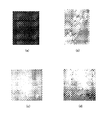
- the triangular figure which shows the composition of the etching liquid used for this invention. Imaging of the surface of a silicon wafer for solar cells. Explanatory drawing of the uneven
- the fixed abrasive method is a method of slicing an ingot using a saw wire in which abrasive grains are bonded and fixed to the surface of the core wire.
- a molten metal method, an electrodeposition method, a resin Bond method is mentioned.
- the molten metal method is a method in which abrasive grains are fixed to the surface of the core wire via a low melting point metal (brazing material) such as a solder alloy, and the method described in JP 2010-201102 A is exemplified.
- the electrodeposition method is a method in which a plating layer is formed on the surface of the core wire by using a plating solution mixed with abrasive particles, thereby fixing the abrasive particles on the surface of the core wire via the plating layer, as described in JP-A-2003-340729. This method is exemplified.
- the resin bond method is a method in which abrasive grains are fixed to the core wire surface with a resin adhesive.
- Steel wire is preferably used as the core wire used in the fixed abrasive system.
- the wire diameter is not particularly limited, but preferably 0.3 to 0.05 mm.
- Steel wire includes heat-treated spring steel wire such as high carbon steel and medium carbon low alloy steel, hard steel wire, piano wire and stainless steel wire, cold rolled steel wire and oil tempered wire wire made of spring steel, low Examples include steel wires with high toughness and high fatigue strength such as alloy steel, medium alloy steel, high alloy steel, and maraging steel.
- the etching solution used in the present invention contains a mixed acid composed of hydrofluoric acid (HF), nitric acid (HNO 3 ), and sulfuric acid (H 2 SO 4 ) as a main component.
- This etchant may further contain water.
- the sulfuric acid concentration is 91 to 97% by weight. If the sulfuric acid concentration is below this range, the etching rate becomes too slow and the etching reaction does not proceed, so it takes too much time for the unevenness to be formed. If it exceeds the range, small concaves are hardly formed, the reflectance is not sufficiently lowered, and the crystal grain contrast difference becomes remarkable.
- the blending ratio of each of the hydrofluoric acid, nitric acid, and sulfuric acid in the etching solution used in the present invention with respect to the total weight of these acids is indicated by a point A ′′ (HF: 1.98) in the triangular diagram shown in FIG.
- the etching solution used in the present invention is, for example, an aqueous solution of hydrofluoric acid having a concentration of 40 to 55 wt% or higher, an aqueous solution of nitric acid having a concentration of 59 to 75 wt% or higher, preferably a concentration of 95 It can be obtained by mixing ⁇ 98 wt% sulfuric acid (a sulfuric acid having a concentration of x% means a mixture of x parts by weight of sulfuric acid and water (100-x) parts by weight).
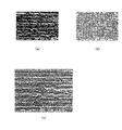
- the silicon wafer for solar cells obtained by the present invention shown in FIG. 2 (a) has irregularities formed by forming a plurality of concave holes having a curved bottom surface on the entire surface.
- the opening diameter of the concave hole is 2 to 15 ⁇ m, and one or more micro holes having an opening diameter of 0.1 to 1.5 ⁇ m are formed on the inner wall of the concave hole.
- the silicon wafer for solar cells of the present invention has irregularities formed by forming a plurality of concave holes over the entire surface, the opening diameter of the concave holes is 2 to 15 ⁇ m, and the inner wall of the concave holes Substantially has a shape in which one or a plurality of micropores having an opening diameter of 0.1 to 1.5 ⁇ m are formed. Such unevenness can be confirmed by a scanning confocal laser microscope or a shape measuring apparatus described in Japanese Patent No. 3810748.
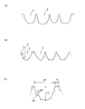
- FIG. 3 is a schematic diagram showing the uneven state of the surface of the silicon wafer for solar cells by a cut surface in the thickness direction of the wafer.
- FIG. 3A is a silicon wafer for solar cells shown in FIG. 3B is a partially enlarged schematic view of FIG. 3B.
- FIG. 3B is a partially enlarged schematic view of the surface of the silicon wafer for solar cells shown in FIG. 2A.
- the silicon wafer for solar cells of the present invention has a large period of irregularities (substantially basal bottom shape) due to large depressions (substantially basal bottom concave holes) 2 when enlarged.
- FIG. 3 there is almost no small depression corresponding to the small depression 3 in FIG.
- the reflectance was 30%, and a sufficiently low surface state could not be formed as compared with FIG. 2 (a) using the etching solution of the present application.
- concave holes are present on the surface of the wafer so that the distance between the upper edges of adjacent concave holes, that is, p is 0 to 10 ⁇ m. Moreover, adjacent concave holes may enter and overlap each other.
- the large indentation 2 is similar to the shape of the indentation of the ridge, and a straight line standing perpendicularly to the wafer surface direction from the deepest part of the depression is used as a symmetrical center line, or from the deepest part of the depression to the wafer surface direction. It has a substantially symmetric shape with a flat plane as a symmetry plane. This indicates that a thin work-affected layer of about 5 ⁇ m is removed by etching, and further etching proceeds in the thickness direction of the wafer to form such a symmetric recess. Due to such symmetrical recesses, irregular reflected light is hardly generated on the wafer surface, and a wafer with less gloss unevenness can be obtained.
- the etching using the etching solution of the present invention can be performed regardless of the presence or absence of a work-affected layer. Accordingly, a basal depression having a symmetrical shape with respect to the thickness direction is formed on the wafer surface.
- the etching solution of the present invention is an etching solution that can form both the large depression 2 and the small depression 3 on the silicon after the work-affected layer has been removed.
- the etching solution of the present invention is an etching solution that can form both the large dent 2 and the small dent 3 on the wafer surface regardless of the presence or absence of the work-affected layer.
- the sliced piece sliced from the polycrystalline silicon ingot by the free abrasive grain method has a thick work-affected layer, unevenness due to crystal grains is generated on the surface only by removing the work-affected layer by etching. It will be.
- the process-affected layer can be removed relatively easily using a conventional etching solution using hydrofluoric acid or nitric acid.
- the depressions obtained in this way are due to the crystal orientation of the crystal grains, and therefore have irregular shapes and asymmetric shapes with respect to the thickness direction of the wafer. For this reason, irregular reflected light tends to be generated on the wafer surface, and a wafer having gloss unevenness can be obtained.
- a work-affected layer having a thickness of 10 ⁇ m or more can be formed even for a polycrystalline silicon wafer having irregular crystal faces.
- a method for obtaining unevenness by etching removal is disclosed (for example, Japanese Patent Laid-Open No. 10-303443, Japanese Patent No. 4766880, etc.). This is because the following reaction proceeds.
- the reaction rate can be changed, and the shape and size of the unevenness can also be changed. It is preferable to add to. The reason for this is as follows.
- the oxidation reaction of silicon reacts a little with concentrated nitric acid as shown above, but when concentrated sulfuric acid is added, an acid / base reaction in which sulfuric acid is an acid and nitric acid is a base occurs.
- an acid / base reaction in which sulfuric acid is an acid and nitric acid is a base occurs.
- the “—O—SO 2 —OH” anion and the “H 2 O (+)-NO 2 ” cation are formed, and the water is released from the “H 2 O (+)-NO 2 ” cation to “(+ ) NO 2 ”cation (nitronium cation) increases in the system.
- Measurement of reflectance of silicon wafers in Examples and Comparative Examples was performed using an ultraviolet-visible near-infrared spectrophotometer Solidspec-3700 and an integrating sphere BIS-3700 manufactured by Shimadzu Corporation. The average value of nine measurements at a wavelength of 600 nm was determined and used as the reflectance.
- Example 1 ⁇ Silicon ingot> A polycrystalline silicon ingot manufactured by GET was used.
- ⁇ Characteristics of silicon wafer> The reflectance of the obtained silicon wafer was 22.0%. d1 was 3 to 14 ⁇ m (average 4.0 ⁇ m), and d2 was 0.1 to 0.5 ⁇ m. Although some uneven gloss was observed on the surface of the silicon wafer, it did not impair the commercial value.
- Example 6 The composition of the etching solution is hydrofluoric acid aqueous solution (concentration 47 wt%) ... 4.2 wt% Nitric acid aqueous solution (concentration 69 wt%) 7.8 wt% Sulfuric acid with a concentration of 95 wt% ... 88.0 wt% Then, the slice piece was immersed in an etching solution at 25 ° C. for 142 seconds and then washed with water to obtain a silicon wafer. Others are the same as in the first embodiment. This composition is displayed as the point of Example 6 in FIG. ⁇ Characteristics of silicon wafer> The reflectance of the obtained silicon wafer was 23.0%. d1 was 2 to 12 ⁇ m (average 4.1 ⁇ m), and d2 was 0.4 to 1.0 ⁇ m. Although some uneven gloss was observed on the surface of the silicon wafer, it did not impair the commercial value.
Landscapes
- Engineering & Computer Science (AREA)
- Mechanical Engineering (AREA)
- Photovoltaic Devices (AREA)
- Weting (AREA)
- Manufacturing & Machinery (AREA)
- Mechanical Treatment Of Semiconductor (AREA)
- Physics & Mathematics (AREA)
- Power Engineering (AREA)
- Processing Of Stones Or Stones Resemblance Materials (AREA)
- Chemical & Material Sciences (AREA)
- Microelectronics & Electronic Packaging (AREA)
- Computer Hardware Design (AREA)
- Finish Polishing, Edge Sharpening, And Grinding By Specific Grinding Devices (AREA)
- Condensed Matter Physics & Semiconductors (AREA)
- General Physics & Mathematics (AREA)
- Polishing Bodies And Polishing Tools (AREA)
- General Chemical & Material Sciences (AREA)
- Chemical Kinetics & Catalysis (AREA)
- ing And Chemical Polishing (AREA)
- Crystallography & Structural Chemistry (AREA)
Priority Applications (3)
| Application Number | Priority Date | Filing Date | Title |
|---|---|---|---|
| CN201480023748.1A CN105144351B (zh) | 2013-04-26 | 2014-04-09 | 太阳能电池用硅晶圆及其制造方法 |
| KR1020157022409A KR20160002683A (ko) | 2013-04-26 | 2014-04-09 | 태양전지용 실리콘 웨이퍼 및 그 제조 방법 |
| SG11201508619VA SG11201508619VA (en) | 2013-04-26 | 2014-04-09 | Silicon wafer for solar cells and method for producing same |
Applications Claiming Priority (4)
| Application Number | Priority Date | Filing Date | Title |
|---|---|---|---|
| JP2013094163 | 2013-04-26 | ||
| JP2013-094163 | 2013-04-26 | ||
| JP2014009159A JP5868437B2 (ja) | 2013-04-26 | 2014-01-22 | 太陽電池用シリコンウエハーの製造方法 |
| JP2014-009159 | 2014-01-22 |
Publications (1)
| Publication Number | Publication Date |
|---|---|
| WO2014175072A1 true WO2014175072A1 (ja) | 2014-10-30 |
Family
ID=51791652
Family Applications (1)
| Application Number | Title | Priority Date | Filing Date |
|---|---|---|---|
| PCT/JP2014/060349 Ceased WO2014175072A1 (ja) | 2013-04-26 | 2014-04-09 | 太陽電池用シリコンウエハー及びその製造方法 |
Country Status (6)
| Country | Link |
|---|---|
| JP (1) | JP5868437B2 (enExample) |
| KR (1) | KR20160002683A (enExample) |
| CN (1) | CN105144351B (enExample) |
| SG (1) | SG11201508619VA (enExample) |
| TW (1) | TW201444955A (enExample) |
| WO (1) | WO2014175072A1 (enExample) |
Cited By (2)
| Publication number | Priority date | Publication date | Assignee | Title |
|---|---|---|---|---|
| JPWO2016098701A1 (ja) * | 2014-12-15 | 2017-09-21 | シャープ株式会社 | 半導体基板の製造方法、光電変換素子の製造方法、半導体基板および光電変換素子 |
| CN118016739A (zh) * | 2024-04-09 | 2024-05-10 | 浙江晶科能源有限公司 | 分片电池及其形成方法、光伏组件 |
Families Citing this family (6)
| Publication number | Priority date | Publication date | Assignee | Title |
|---|---|---|---|---|
| JP2014232829A (ja) * | 2013-05-30 | 2014-12-11 | 日本化成株式会社 | 太陽電池用シリコンウエハーの製造方法 |
| TWI538986B (zh) * | 2015-07-15 | 2016-06-21 | 綠能科技股份有限公司 | 蝕刻液以及矽基板的表面粗糙化的方法 |
| WO2017091572A1 (en) | 2015-11-23 | 2017-06-01 | Entegris, Inc. | Composition and process for selectively etching p-doped polysilicon relative to silicon nitride |
| CN108183067A (zh) * | 2018-01-05 | 2018-06-19 | 苏州同冠微电子有限公司 | 一种半导体晶圆的处理方法 |
| CN111748806B (zh) * | 2020-07-21 | 2022-08-23 | 江苏悦锌达新材料有限公司 | 一种用于聚苯硫醚及其复合材料的粗化液及其制备方法和使用方法 |
| CN112233967B (zh) * | 2020-10-15 | 2024-05-03 | 扬州扬杰电子科技股份有限公司 | 一种改善背面金属与衬底Si脱落异常的加工方法 |
Citations (5)
| Publication number | Priority date | Publication date | Assignee | Title |
|---|---|---|---|---|
| JP2004193369A (ja) * | 2002-12-11 | 2004-07-08 | Denso Corp | 半導体装置の製造方法およびそれにより製造される半導体装置 |
| US20100151678A1 (en) * | 2008-12-15 | 2010-06-17 | Mark Dydyk | Wafer Backside Grinding with Stress Relief |
| WO2012102368A1 (ja) * | 2011-01-27 | 2012-08-02 | 京セラ株式会社 | 太陽電池素子の製造方法、太陽電池素子、および太陽電池モジュール |
| JP2012169420A (ja) * | 2011-02-14 | 2012-09-06 | Sumco Corp | 太陽電池用ウェーハの製造方法、太陽電池セルの製造方法および太陽電池モジュールの製造方法 |
| JP2013505562A (ja) * | 2009-09-21 | 2013-02-14 | ビーエーエスエフ ソシエタス・ヨーロピア | 水性酸エッチング溶液、単結晶及び多結晶のシリコン基板の表面のテクスチャリング方法 |
Family Cites Families (15)
| Publication number | Priority date | Publication date | Assignee | Title |
|---|---|---|---|---|
| JPH09270400A (ja) | 1996-01-31 | 1997-10-14 | Shin Etsu Handotai Co Ltd | 半導体ウェーハの製造方法 |
| JP4024934B2 (ja) | 1998-08-10 | 2007-12-19 | 住友電気工業株式会社 | ワイヤーソー及びその製造方法 |
| DE19962136A1 (de) * | 1999-12-22 | 2001-06-28 | Merck Patent Gmbh | Verfahren zur Rauhätzung von Siliziumsolarzellen |
| JP2004503081A (ja) | 2000-06-30 | 2004-01-29 | エムイーエムシー・エレクトロニック・マテリアルズ・インコーポレイテッド | シリコンウェーハのエッチング方法 |
| JP2004063954A (ja) | 2002-07-31 | 2004-02-26 | Sumitomo Mitsubishi Silicon Corp | シリコンウェーハのエッチング方法及びこの方法を用いたシリコンウェーハの表裏面差別化方法 |
| JP4231049B2 (ja) | 2003-10-10 | 2009-02-25 | 三益半導体工業株式会社 | ウェーハの粗面処理方法 |
| JP4430488B2 (ja) | 2004-09-02 | 2010-03-10 | シャープ株式会社 | 太陽電池及びその製造方法 |
| JP4766880B2 (ja) * | 2005-01-18 | 2011-09-07 | シャープ株式会社 | 結晶シリコンウエハ、結晶シリコン太陽電池、結晶シリコンウエハの製造方法および結晶シリコン太陽電池の製造方法 |
| DE102010012044A1 (de) * | 2010-03-19 | 2011-09-22 | Friedrich-Schiller-Universität Jena | Strukturierte Siliziumschicht für ein optoelektronisches Bauelement und optoelektronisches Bauelement |
| JP2011255475A (ja) | 2010-06-11 | 2011-12-22 | Takatori Corp | 固定砥粒ワイヤ |
| JP2012024866A (ja) | 2010-07-21 | 2012-02-09 | Sumco Corp | ワイヤソー切断スラッジの回収方法およびその装置 |
| KR101657626B1 (ko) * | 2010-10-08 | 2016-09-19 | 주식회사 원익아이피에스 | 태양전지제조방법 및 그 방법에 의하여 제조된 태양전지 |
| JP2012222300A (ja) * | 2011-04-13 | 2012-11-12 | Panasonic Corp | テクスチャ形成面を有するシリコン基板、およびその製造方法 |
| JP5780856B2 (ja) | 2011-06-30 | 2015-09-16 | 京セラ株式会社 | 積層セラミックコンデンサ |
| JP2013043268A (ja) | 2011-08-26 | 2013-03-04 | Sharp Corp | 固定砥粒ワイヤおよび半導体基板の製造方法 |
-
2014
- 2014-01-22 JP JP2014009159A patent/JP5868437B2/ja not_active Expired - Fee Related
- 2014-04-09 WO PCT/JP2014/060349 patent/WO2014175072A1/ja not_active Ceased
- 2014-04-09 CN CN201480023748.1A patent/CN105144351B/zh not_active Expired - Fee Related
- 2014-04-09 KR KR1020157022409A patent/KR20160002683A/ko not_active Ceased
- 2014-04-09 SG SG11201508619VA patent/SG11201508619VA/en unknown
- 2014-04-18 TW TW103114268A patent/TW201444955A/zh unknown
Patent Citations (5)
| Publication number | Priority date | Publication date | Assignee | Title |
|---|---|---|---|---|
| JP2004193369A (ja) * | 2002-12-11 | 2004-07-08 | Denso Corp | 半導体装置の製造方法およびそれにより製造される半導体装置 |
| US20100151678A1 (en) * | 2008-12-15 | 2010-06-17 | Mark Dydyk | Wafer Backside Grinding with Stress Relief |
| JP2013505562A (ja) * | 2009-09-21 | 2013-02-14 | ビーエーエスエフ ソシエタス・ヨーロピア | 水性酸エッチング溶液、単結晶及び多結晶のシリコン基板の表面のテクスチャリング方法 |
| WO2012102368A1 (ja) * | 2011-01-27 | 2012-08-02 | 京セラ株式会社 | 太陽電池素子の製造方法、太陽電池素子、および太陽電池モジュール |
| JP2012169420A (ja) * | 2011-02-14 | 2012-09-06 | Sumco Corp | 太陽電池用ウェーハの製造方法、太陽電池セルの製造方法および太陽電池モジュールの製造方法 |
Cited By (2)
| Publication number | Priority date | Publication date | Assignee | Title |
|---|---|---|---|---|
| JPWO2016098701A1 (ja) * | 2014-12-15 | 2017-09-21 | シャープ株式会社 | 半導体基板の製造方法、光電変換素子の製造方法、半導体基板および光電変換素子 |
| CN118016739A (zh) * | 2024-04-09 | 2024-05-10 | 浙江晶科能源有限公司 | 分片电池及其形成方法、光伏组件 |
Also Published As
| Publication number | Publication date |
|---|---|
| KR20160002683A (ko) | 2016-01-08 |
| JP2014225633A (ja) | 2014-12-04 |
| TW201444955A (zh) | 2014-12-01 |
| JP5868437B2 (ja) | 2016-02-24 |
| CN105144351A (zh) | 2015-12-09 |
| SG11201508619VA (en) | 2015-12-30 |
| CN105144351B (zh) | 2017-09-26 |
Similar Documents
| Publication | Publication Date | Title |
|---|---|---|
| JP5868437B2 (ja) | 太陽電池用シリコンウエハーの製造方法 | |
| AU780184B2 (en) | Method for raw etching silicon solar cells | |
| TWI494416B (zh) | 用於蝕紋單晶及多晶矽基板表面之酸性蝕刻溶液及方法 | |
| US9876128B2 (en) | Texturing monocrystalline silicon substrates | |
| WO2011024910A1 (ja) | 太陽電池用シリコンウェーハおよびその製造方法 | |
| CN108381797A (zh) | 环形金刚石线锯及其制造方法 | |
| US20090042390A1 (en) | Etchant for silicon wafer surface shape control and method for manufacturing silicon wafers using the same | |
| US9051664B2 (en) | Nanostructuring process for ingot surface, water manufacturing method, and wafer using the same | |
| WO2009153887A1 (ja) | インゴットスライシング用フレットバー、該フレットバーを貼着したインゴット、及び該フレットバーを用いたインゴットの切断方法 | |
| TWI853209B (zh) | 自半導體材料的圓柱形錠生產晶圓的方法 | |
| JP2013110327A (ja) | 太陽電池用シリコン基板の製造方法 | |
| JP5957835B2 (ja) | 太陽電池用ウェーハの製造方法、太陽電池セルの製造方法、および太陽電池モジュールの製造方法 | |
| CN103160930A (zh) | 晶棒表面纳米化工艺、晶圆制造方法及其晶圆 | |
| WO2018025539A1 (ja) | シリコンインゴットの切断方法、シリコンウェーハの製造方法およびシリコンウェーハ | |
| CN204955160U (zh) | 一种金刚石钎焊线锯 | |
| US20090060821A1 (en) | Method for manufacturing silicone wafers | |
| CN206568357U (zh) | 三丝绞合切割钢线 | |
| JP2015088712A (ja) | テクスチャエッチング液、テクスチャエッチング液用添加剤液、テクスチャ形成基板及びテクスチャ形成基板の製造方法並びに太陽電池 | |
| KR102255578B1 (ko) | Kerfless 방식으로 제작된 실리콘 웨이퍼의 습식 이단계 표면조직화 방법 | |
| JP2015145042A (ja) | ワイヤー工具 | |
| JP2009179726A (ja) | 研削・研磨用炭化珪素粉末の製造方法及び研削・研磨用炭化珪素粉末並びに研削・研磨用スラリー | |
| CN103572291B (zh) | 电镀金刚石线锯镀层用腐蚀液及线锯断线连接方法 | |
| JP2003007672A (ja) | シリコン半導体ウェーハのエッチング方法 | |
| CN208930497U (zh) | 一种钻石线及线锯 | |
| JP2006210759A (ja) | シリコンウェーハ表面形状制御用エッチング液及び該エッチング液を用いたシリコンウェーハの製造方法 |
Legal Events
| Date | Code | Title | Description |
|---|---|---|---|
| WWE | Wipo information: entry into national phase |
Ref document number: 201480023748.1 Country of ref document: CN |
|
| 121 | Ep: the epo has been informed by wipo that ep was designated in this application |
Ref document number: 14788078 Country of ref document: EP Kind code of ref document: A1 |
|
| ENP | Entry into the national phase |
Ref document number: 20157022409 Country of ref document: KR Kind code of ref document: A |
|
| WWE | Wipo information: entry into national phase |
Ref document number: IDP00201505787 Country of ref document: ID |
|
| NENP | Non-entry into the national phase |
Ref country code: DE |
|
| 122 | Ep: pct application non-entry in european phase |
Ref document number: 14788078 Country of ref document: EP Kind code of ref document: A1 |