WO2014174853A1 - ボイスコイルモータの駆動回路およびそれを用いたレンズモジュールおよび電子機器 - Google Patents
ボイスコイルモータの駆動回路およびそれを用いたレンズモジュールおよび電子機器 Download PDFInfo
- Publication number
- WO2014174853A1 WO2014174853A1 PCT/JP2014/002340 JP2014002340W WO2014174853A1 WO 2014174853 A1 WO2014174853 A1 WO 2014174853A1 JP 2014002340 W JP2014002340 W JP 2014002340W WO 2014174853 A1 WO2014174853 A1 WO 2014174853A1
- Authority
- WO
- WIPO (PCT)
- Prior art keywords
- voltage
- error
- drive circuit
- detection
- voice coil
- Prior art date
- Legal status (The legal status is an assumption and is not a legal conclusion. Google has not performed a legal analysis and makes no representation as to the accuracy of the status listed.)
- Ceased
Links
Images


Classifications
-
- H—ELECTRICITY
- H02—GENERATION; CONVERSION OR DISTRIBUTION OF ELECTRIC POWER
- H02P—CONTROL OR REGULATION OF ELECTRIC MOTORS, ELECTRIC GENERATORS OR DYNAMO-ELECTRIC CONVERTERS; CONTROLLING TRANSFORMERS, REACTORS OR CHOKE COILS
- H02P25/00—Arrangements or methods for the control of AC motors characterised by the kind of AC motor or by structural details
- H02P25/02—Arrangements or methods for the control of AC motors characterised by the kind of AC motor or by structural details characterised by the kind of motor
- H02P25/032—Reciprocating, oscillating or vibrating motors
- H02P25/034—Voice coil motors
-
- G—PHYSICS
- G02—OPTICS
- G02B—OPTICAL ELEMENTS, SYSTEMS OR APPARATUS
- G02B7/00—Mountings, adjusting means, or light-tight connections, for optical elements
- G02B7/02—Mountings, adjusting means, or light-tight connections, for optical elements for lenses
- G02B7/04—Mountings, adjusting means, or light-tight connections, for optical elements for lenses with mechanism for focusing or varying magnification
-
- G—PHYSICS
- G02—OPTICS
- G02B—OPTICAL ELEMENTS, SYSTEMS OR APPARATUS
- G02B7/00—Mountings, adjusting means, or light-tight connections, for optical elements
- G02B7/02—Mountings, adjusting means, or light-tight connections, for optical elements for lenses
- G02B7/04—Mountings, adjusting means, or light-tight connections, for optical elements for lenses with mechanism for focusing or varying magnification
- G02B7/08—Mountings, adjusting means, or light-tight connections, for optical elements for lenses with mechanism for focusing or varying magnification adapted to co-operate with a remote control mechanism
-
- H—ELECTRICITY
- H02—GENERATION; CONVERSION OR DISTRIBUTION OF ELECTRIC POWER
- H02P—CONTROL OR REGULATION OF ELECTRIC MOTORS, ELECTRIC GENERATORS OR DYNAMO-ELECTRIC CONVERTERS; CONTROLLING TRANSFORMERS, REACTORS OR CHOKE COILS
- H02P25/00—Arrangements or methods for the control of AC motors characterised by the kind of AC motor or by structural details
- H02P25/02—Arrangements or methods for the control of AC motors characterised by the kind of AC motor or by structural details characterised by the kind of motor
- H02P25/06—Linear motors
-
- H—ELECTRICITY
- H04—ELECTRIC COMMUNICATION TECHNIQUE
- H04N—PICTORIAL COMMUNICATION, e.g. TELEVISION
- H04N23/00—Cameras or camera modules comprising electronic image sensors; Control thereof
- H04N23/60—Control of cameras or camera modules
-
- G—PHYSICS
- G03—PHOTOGRAPHY; CINEMATOGRAPHY; ANALOGOUS TECHNIQUES USING WAVES OTHER THAN OPTICAL WAVES; ELECTROGRAPHY; HOLOGRAPHY
- G03B—APPARATUS OR ARRANGEMENTS FOR TAKING PHOTOGRAPHS OR FOR PROJECTING OR VIEWING THEM; APPARATUS OR ARRANGEMENTS EMPLOYING ANALOGOUS TECHNIQUES USING WAVES OTHER THAN OPTICAL WAVES; ACCESSORIES THEREFOR
- G03B2205/00—Adjustment of optical system relative to image or object surface other than for focusing
- G03B2205/0053—Driving means for the movement of one or more optical element
- G03B2205/0069—Driving means for the movement of one or more optical element using electromagnetic actuators, e.g. voice coils
Definitions
- the present invention relates to a voice coil motor control technique.
- An actuator for positioning a focusing lens is provided in a digital still camera, a digital video camera, or an electronic device with an imaging function (for example, a mobile phone).
- a stepping motor method, a piezo method, a voice coil motor (VCM) method, or the like is employed as the actuator.
- VCM can generate a propulsive force in a linear direction according to the direction of current flowing through the coil.
- a VCM drive system a spring return system and a bidirectional drive system are known.
- a VCM with a spring return mechanism generates a propulsive force in a first direction by supplying a drive current to a coil, and a propulsive force in a second direction opposite to that of a spring (spring) attached to the mover. It has a structure that uses force to generate. That is, electric drive and dynamic drive are used together. When driving a VCM with a spring return mechanism, it is sufficient to supply a drive current only in one direction of the coil, and the drive circuit can be simplified.
- a drive circuit that can source and sink drive current from both ends of the VCM, such as an H bridge circuit, is used.
- the direction of the coil current can be switched, and a propulsive force can be obtained in the positive direction and the negative direction.
- the bidirectional driving method is advantageous from the viewpoint of reducing power consumption because the driving current of the VCM can be made substantially zero at any reference displacement position.
- a conventional bidirectional driving type driving circuit is configured symmetrically. Now, assuming that the direction of the current flowing in the VCM coil in the first direction is positive, the drive circuit is configured to be able to generate a drive current in the range of ⁇ I MAX to I MAX centering on a current value of zero. Is done.
- the optimum drive current range may differ depending on the manufacturer and model of the VCM to be driven or the set on which the VCM is mounted.
- the present invention has been made in view of the above problems, and one of the exemplary purposes of an aspect thereof is to provide a VCM drive circuit capable of setting a current range.
- An error amplifier that generates an error voltage by amplifying an error between a control voltage indicating a quantity and a detection voltage and one end of a coil of a voice coil motor are connected to source or sink a drive current according to the error voltage.
- a first driver and a second driver connected to the other end of the coil of the voice coil motor and sinking or sourcing driving current according to an error voltage.
- This drive circuit is configured such that the level of the reference voltage V REF can be set from the outside.
- the relative relationship between the control voltage and the drive current I DRV can be shifted according to the reference voltage V REF , and the drive current range can be arbitrarily set.
- the current detection circuit includes a detection resistor provided on the drive current path, a first operational amplifier, a first resistor provided between the first input terminal of the first operational amplifier and the first end of the detection resistor. , A second resistor provided between the second input terminal of the first operational amplifier and the second end of the detection resistor, and provided between the output terminal of the first operational amplifier and the first input terminal of the first operational amplifier.
- the third resistor may include a fourth resistor having one end connected to the second input terminal of the first operational amplifier and the other end to which a reference voltage is applied.
- a driving circuit includes a first D / A converter that converts digital control data indicating an amount of displacement from an external processor into an analog control voltage, and correction data indicating a reference voltage from the external processor as an analog reference. And a second D / A converter for converting the voltage into a voltage. According to this configuration, the range of the drive current generated corresponding to the range of the digital control data can be arbitrarily set according to the value of the correction data.
- the detection resistor may be provided between the first end of the coil and the output end of the first driver, or between the second end of the coil and the output end of the second driver.
- the on-resistance of a transistor constituting the output stage of the first driver and the on-resistance of a transistor constituting the output stage of the second driver may be used.
- the known DC resistance component of the voice coil motor may be used as the detection resistance.
- the error amplifier includes a second operational amplifier in which a control voltage is input to the first input terminal, a first capacitor provided between the second input terminal of the second operational amplifier and its output terminal, and a first terminal thereof. May be connected to the second input terminal of the second operational amplifier, and may include a fifth resistor to which the detection voltage is applied to the second terminal.
- the first driver may include a non-inverting amplifier that non-inverts and amplifies the error voltage with a predetermined common voltage as a reference, and applies the first driving voltage to the first end of the coil.
- the second driver may include an inverting amplifier that inverts and amplifies the error voltage with reference to the common voltage and applies the second drive voltage to the second terminal of the coil.
- the first driver has a first voltage dividing circuit for dividing a first output voltage generated at the first end of the coil and a predetermined common voltage at a predetermined voltage dividing ratio, and a push-pull output stage including a high side transistor and a low side transistor. And a first amplifier that controls the high-side transistor and the low-side transistor of the push-pull output stage so that the voltage divided by the first voltage dividing circuit is equal to the error voltage.
- the second driver has a second voltage dividing circuit that divides the second output voltage and the error voltage generated at the second end of the coil at a predetermined voltage dividing ratio, and a second push-pull output stage including a high side transistor and a low side transistor. And a second amplifier that controls the high-side transistor and the low-side transistor of the push-pull output stage so that the voltage divided by the second voltage dividing circuit is equal to the common voltage.
- Another aspect of the present invention also relates to a drive circuit that supplies a bidirectional drive current to a voice coil motor.
- This drive circuit includes a current detection circuit that generates a detection voltage Vs corresponding to the drive current, and an error amplifier that generates an error voltage by amplifying an error between a control voltage indicating the displacement amount of the voice coil motor and the detection voltage. And connected to one end of the coil of the voice coil motor and connected to the first driver that sources or sinks the drive current according to the error voltage and connected to the other end of the coil of the voice coil motor and driven according to the error voltage. And a second driver that sinks or sources current.
- This drive circuit is configured so that a shift voltage that can be set from the outside can be superimposed on at least one of the control voltage and the detection voltage, and the error amplifier has the same control voltage and detection voltage with the shift voltage superimposed on at least one of them. Thus, an error voltage is generated.
- the relative relationship between the control voltage and the drive current IDRV can be shifted according to the shift voltage, and the range of the drive current can be arbitrarily set.
- the level of the reference voltage V REF may be configured to be set according to correction data from an external processor. In this case, the shift voltage superimposed on the detection voltage can be controlled according to the correction data.
- the control voltage may be a voltage obtained by adding a shift voltage corresponding to correction data from the external processor to a voltage corresponding to digital control data indicating the displacement amount of the voice coil motor from the external processor.
- a shift voltage corresponding to the correction data can be superimposed on the control voltage.
- the control voltage may be a voltage obtained by converting a digital value obtained by adding or subtracting digital control data indicating the amount of displacement of the voice coil motor from the external processor and correction data from the external processor into an analog voltage. In this case, a shift voltage corresponding to the correction data can be superimposed on the control voltage.
- a shift voltage corresponding to the correction data can be superimposed on the control voltage.
- the error amplifier offset voltage may be adjustable in accordance with the correction data from the external processor.
- the drive circuit may be integrated on a single semiconductor substrate. “Integrated integration” includes the case where all of the circuit components are formed on a semiconductor substrate and the case where the main components of the circuit are integrated. A resistor, a capacitor, or the like may be provided outside the semiconductor substrate.
- the lens module includes a focusing lens, a voice coil motor with a bidirectional or spring return mechanism whose movable element is coupled to the focusing lens, and a drive circuit according to any one of the above-described modes for driving the voice coil motor.
- the lens module includes a camera shake correction lens, a voice coil motor with a bidirectional or spring return mechanism in which a movable element is coupled to the camera shake correction lens, and a drive circuit according to any one of the above-described modes for driving the voice coil motor. .
- the electronic device includes any one of the lens modules described above and an imaging element that captures an image of light that has passed through the lens module.
- the drive current range can be set.
- the state in which the member A is connected to the member B means that the member A and the member B are electrically connected to each other in addition to the case where the member A and the member B are physically directly connected. It includes cases where the connection is indirectly made through other members that do not substantially affect the general connection state, or that do not impair the functions and effects achieved by their combination.
- the state in which the member C is provided between the member A and the member B refers to the case where the member A and the member C or the member B and the member C are directly connected, as well as their electric It includes cases where the connection is indirectly made through other members that do not substantially affect the general connection state, or that do not impair the functions and effects achieved by their combination.
- FIG. 1 is a block diagram illustrating an overall configuration of an electronic device 500 according to an embodiment.
- the electronic device 500 is a mobile phone with an imaging function, a digital camera, a video camera, a WEB camera, a tablet PC (Personal Computer), or the like, and includes a lens module 502, an image sensor 504, an image processor 506, and a CPU (Central Processing Unit). 508.
- a lens module 502 an image sensor 504, an image processor 506, and a CPU (Central Processing Unit). 508.
- CPU Central Processing Unit
- the lens module 502 is provided to realize a so-called autofocus function, and includes a focusing lens 512 and an actuator 510.
- the lens 512 is supported so as to be movable in the optical axis direction.
- the actuator 510 controls the position of the lens 512 based on the command value S1 from the CPU 508.
- the light (image) that has passed through the lens 512 is incident on the image sensor 504.
- the image processor 506 reads image data from the image sensor 504.
- the CPU 508 determines the target position of the focusing lens 512 based on the image read by the image processor 506 so that the image that has passed through the focusing lens 512 is formed on the image sensor 504, and sets the target position to the target position.
- the corresponding command value S1 is output to the actuator 510.
- the above is the overall configuration of the electronic device 500. Next, a specific configuration of the lens module 502 will be described.
- FIG. 2 is a block diagram illustrating a configuration of the lens module 502 according to the embodiment.
- the lens module 502 includes a voice coil motor (VCM) 200 and the drive circuit 2.
- VCM voice coil motor
- the VCM 200 is an actuator for positioning a focusing lens (512 in FIG. 1), and the movable element is connected to the focusing lens.
- the drive circuit 2 has output terminals OUT + and OUT ⁇ , a power supply terminal PVDD, a ground terminal PGND, and an interface terminal IF.
- a power supply voltage V DD is supplied to the power supply terminal PVDD, and a ground voltage V GND is supplied to the ground terminal PGND.
- Interface terminal IF is connected via an external CPU 508 and the bus, the drive circuit 2 from CPU 508, the stroke amount of the movable element of VCM 200 (target position, displacement) control data D CNT instructing supply Is done.
- the drive circuit 2 includes a current detection circuit 10, an error amplifier 20, a first driver 30, a second driver 40, a logic unit 50, a first D / A converter 52, a second D / A converter 54, and a buffer 56.
- the logic unit 50 includes an interface circuit that transmits and receives data and commands to and from the CPU 508, a register that stores data received from the CPU 508, and the like.
- the current detection circuit 10 detects the drive current I DRV flowing through the coil L1 and generates a detection voltage Vs corresponding to the drive current I DRV .
- the detection voltage Vs is given by the following equation (2) using the gain k and the reference voltage VREF .
- Vs V REF + k ⁇ I DRV (2)
- the current detection circuit 10 includes a detection resistor R NF , a first resistor R 1, a second resistor R 2, a third resistor R 3, and a fourth resistor R 4.
- the detection resistor R NF is provided on the path of the drive current I DRV .
- the detection resistor RNF is provided between the second end of the coil L1 and the output end of the second driver 40.
- the detection resistor RNF may be provided between the first end of the coil L1 and the output end of the first driver 30.
- a voltage drop V NF proportional to the drive current I DRV is generated in the detection resistor R FN .
- the first resistor R1 is provided between the first input terminal (inverting input terminal) of the first operational amplifier 12 and the first end E1 of the detection resistor RNF .
- the second resistor R2 is provided between the second input terminal (non-inverting input terminal) of the first operational amplifier 12 and the second end E2 of the detection resistor RNF .
- the third resistor R3 is provided between the output terminal of the first operational amplifier 12 and the first input terminal (inverting input terminal).
- One end of the fourth resistor R4 is connected to the second input terminal (non-inverting input terminal) of the first operational amplifier 12, and the reference voltage VREF is applied to the other end.
- Detection resistor R NF first end E1 of the second terminal E2 respective potentials and V1, V2.
- the detection voltage Vs is given by equation (3).
- Vs V REF + Rb / Ra ⁇ (V2 ⁇ V1) (3)
- equation (4) into equation (3) yields equation (5).
- Vs V REF + Rb / Ra ⁇ R NF ⁇ I DRV (5) Therefore, the gain k of the current detection circuit 10 is Rb / Ra ⁇ RNF .
- the configuration of the current detection circuit 10 is not limited to that of FIG. 2, and other configurations may be used.
- the 1D / A converter 52, a logic unit 50 converts the control data D CNT received from the CPU508 of the control voltage V CNT analog.
- the control voltage V CNT indicates the target stroke amount of the mover of the VCM 200.
- the drive circuit 2 is configured such that the level of the reference voltage VREF can be set from the outside.
- the logic unit 50 is configured to be able to receive correction data D REF instructing the reference voltage V REF from the CPU 508.
- the second D / A converter 54 converts the correction data D REF received by the logic unit 50 into an analog reference voltage V REF .
- the control voltage VCNT is input to the first input terminal (non-inverting input terminal) of the second operational amplifier 22.
- the first capacitor C1 is provided between the second input terminal (inverting input terminal) of the second operational amplifier 22 and its output terminal.
- the first end of the fifth resistor R5 is connected to the second input terminal (inverting input terminal) of the second operational amplifier 22, and the detection voltage Vs is applied to the second end.
- the first driver 30 is connected to one end of the coil L1 of the voice coil motor 200, and sources or sinks the drive current I DRV according to the error voltage VERR .
- the second driver 40 operates in a phase opposite to that of the first driver 30, is connected to the other end of the coil L1 of the voice coil motor 200, and sinks or sources the drive current IDRV according to the error voltage VERR .
- the buffer 56 outputs a predetermined common voltage VCOM .
- the first driver 30 includes a non-inverting amplifier that non-inverts and amplifies the error voltage V ERR with respect to the common voltage V COM and applies the first drive voltage V O + to the first end of the coil L1.
- the second driver 40 inverts and amplifies the error voltage V ERR with the common voltage V COM as a reference, and applies a second drive voltage V O ⁇ having a phase opposite to that of the first drive voltage V O + to the second terminal of the coil L1. Including an inverting amplifier.
- the first driver 30 includes a first voltage dividing circuit 32 and a first amplifier 34.
- the first voltage dividing circuit 32 includes resistors R11 and R12, and divides the first output voltage V O + generated at the first end of the coil L1 and the predetermined common voltage V COM at a predetermined voltage dividing ratio.
- the first amplifier 34 has a push-pull output stage composed of a high side transistor MH and a low side transistor ML. The first amplifier 34 controls the high-side transistor MH and the low-side transistor ML in the push-pull output stage so that the voltage V FB + divided by the first voltage dividing circuit 32 becomes equal to the error voltage V ERR .
- 3A to 3C are diagrams showing the input / output characteristics of the drive circuit 2 of FIG.
- the control data D CNT from the CPU 508 is 10 bits, and the value can take 0x000 (0) to 0x3FF (1023).
- the control voltage V CNT is the lower reference voltage V L (for example, 0 V) of the first D / A converter 52.
- the control voltage V CNT is a upper reference voltage V H of the 1D / a converter 52.
- the drive circuit 2 generates drive voltages V O + and V O ⁇ by a feedback loop including the error amplifier 20 so that the detected voltage Vs matches the control voltage V CNT .
- the voltage range of the control voltage V CNT is 0 to V H
- the change width ⁇ I I MAX ⁇ I MIN of the drive current I DRV is V H / k, and is constant regardless of the value of the reference voltage V REF .
- the drive circuit 2 is configured such that the reference voltage V REF supplied to the current detection circuit 10 can be set according to reference data D REF from the external CPU 508. Since the reference voltage V REF does not require the same resolution as the control voltage V CNT , the number of bits of the second D / A converter 54 may be about 8 bits, and the reference data D REF is also given by 8 bits.
- V REF V H ⁇ Y / 255 ⁇ V H ⁇ (4 ⁇ Y) / 1023 It becomes. That is, when the control data D CNT is equal to the value obtained by quadrupling the reference data D REF (shifted to the upper side of 2 bits), the drive current I DRV becomes zero.
- FIG. 3 (b) the reference voltage V REF as a parameter, a control relationship between the voltage V CNT and the driving current I DRV is shown in FIG. 3 (c), the reference data D REF for instructing the reference voltage V REF As a parameter, the relationship between the control data DCNT and the drive current IDRV is shown.
- I MAX ⁇ I / 1023 ⁇ (1023 ⁇ (Y ⁇ 4))
- I MIN ⁇ I / 1023 ⁇ ( ⁇ Y ⁇ 4)
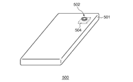
- FIG. 4 is a perspective view showing a mobile phone terminal as an example of the electronic apparatus 500.
- the electronic device 500 includes a housing 501, a lens module 502, and an image sensor 504.
- the image sensor 504 is built in the housing 501.
- the housing 501 is provided with an opening at a location overlapping with the imaging element 504, and the lens module 502 is provided in the opening.
- the drive circuit 2 only needs to be configured so that a shift voltage that can be set from the outside can be superimposed on at least one of the control voltage VCNT and the detection voltage Vs.
- the error amplifier 20 may generate the error voltage V ERR so that the control voltage V CNT with the shift voltage superimposed on at least one and the detection voltage Vs are equal.
- a shift voltage that can be set according to correction data from the outside is superimposed (added or subtracted) on the detection voltage Vs.
- This aspect includes the following techniques. 1.1
- the reference voltage V REF is variable. This has been described in the embodiment.
- the analog summing means for adding or subtracting a shift voltage corresponding to the correction data D REF provided. Then, the output voltage of the analog addition / subtraction means is output to the error amplifier 20.
- a shift voltage that can be set according to external correction data is superimposed (added or subtracted) on the control voltage VCNT .
- This aspect includes the following techniques. Between 2.1 error amplifier 20 of the first 1D / A converter 52, providing the analog summing means for adding or subtracting a shift voltage corresponding to the control voltage V CNT and the correction data D REF. Then, the output voltage of the analog addition / subtraction means is output to the error amplifier 20. 2.2 Digital control data D CNT and correction data D REF are combined (added or subtracted) by digital calculation, and the obtained digital value is D / A converted by the first D / A converter 52 and supplied to the error amplifier 20. Supply.
- the input offset voltage of the error amplifier 20 (second operational amplifier 22) is variable, and the offset voltage of the error amplifier 20 can be adjusted according to the correction data from the external processor.
- Modification 2 In the embodiment, a case has been described of providing a detection resistor R NF between the second driver 40 (first driver 30) and the coil L1, the position of the detection resistor R NF is not limited thereto.
- the detection resistor R NF may be provided in series with the high-side transistor MH between the output terminal OUT + (OUT ⁇ ) and the power supply line, or in series with the low-side transistor ML between the output terminal OUT + (OUT ⁇ ) and the ground line. May be provided.
- the on-resistance of the transistors (MH, ML) constituting the output stage of the first driver 30 and / or the on-resistance of the transistors (MH, ML) constituting the output stage of the second driver 40 May be used.
- the resistance value may be used as the detection resistor R NF.
- the voltage across the VCM 200 is the sum of the voltage drop that occurs in the resistance component and the back electromotive force that occurs in the inductance L1. Therefore, the current detection circuit 10 may remove the counter electromotive force generated in the coil L1 from the voltage between both ends of the VCM 200 and detect the voltage drop of the resistance component.
- a known technique can be used for such a current detection circuit.
- the CPU 508 although the digital control data D CNT and the reference data D REF has been described the case where given, the present invention is not limited thereto.
- the drive circuit 2 at least one pin for setting the reference voltage V REF provided, each pin state (high-level voltage, low voltage or high impedance) according to the combination of the reference voltage V REF It may be set.
- the drive circuit 2 may receive an analog reference voltage VREF from the outside.
- the drive circuit 2 may receive an analog control voltage VCNT from the outside.
- the lens module for focusing has been described, but the application of the drive circuit 2 is not limited thereto.
- the VCM 200 may drive a camera shake correction lens.
- DESCRIPTION OF SYMBOLS 500 ... Electronic device, 501 ... Housing, 502 ... Lens module, 504 ... Image sensor, 506 ... Image processor, 508 ... CPU, 510 ... Actuator, 512 ... Lens, 2 ... Drive circuit, OUT ... Output terminal, 10 ... Current detection circuit, 12 ... first operational amplifier, RNF ... detection resistor, R1 ... first resistor, R2 ... second resistor, R3 ... third resistor, R4 ... fourth resistor, 20 ... error amplifier, 22 ... second Operational amplifier, C1... First capacitor, R5... Fifth resistor, 30... First driver, 32... First voltage dividing circuit, 34. ... second amplifier, 50 ... logic unit, 200 ... VCM, L1 ... coil, 52 ... first D / A converter, 54 ... second D / A converter, 56 ... buffer.
- the present invention can be used for an actuator or the like.
Landscapes
- Physics & Mathematics (AREA)
- Engineering & Computer Science (AREA)
- General Physics & Mathematics (AREA)
- Optics & Photonics (AREA)
- Power Engineering (AREA)
- Multimedia (AREA)
- Signal Processing (AREA)
- Control Of Linear Motors (AREA)
- Lens Barrels (AREA)
Abstract
電流検出回路10は、駆動電流をIDRV、基準電圧をVREF、利得をkとするとき、Vs=VREF+k×IDRVで与えられる検出電圧Vsを生成する。誤差増幅器20は、VCM200の変位量を指示する制御電圧VCNTと検出電圧Vsとの誤差を増幅することにより誤差電圧VERRを生成する。第1ドライバ30は、誤差電圧VERRに応じて、コイルL1の一端に駆動電流IDRVをソースまたはシンクする。第2ドライバ40は、誤差電圧VERRに応じて、コイルL1の他端に駆動電流IDRVをシンクまたはソースする。駆動回路2は、基準電圧VREFのレベルが外部から設定可能に構成される。
Description
本発明は、ボイスコイルモータの制御技術に関する。
デジタルスチルカメラ、デジタルビデオカメラあるいは撮像機能付きの電子機器(たとえば携帯電話)には、フォーカシングレンズを位置決めするためのアクチュエータが設けられる。アクチュエータとしてはステッピングモータ方式、ピエゾ方式、ボイスコイルモータ(VCM)方式等が採用される。
VCMは、そのコイルに流れる電流の向きに応じた直線方向に推進力を発生させることができる。VCMの駆動方式としては、スプリングリターン方式と、双方向駆動方式が知られている。
スプリングリターン機構付きVCMは、第1の方向への推進力をコイルに駆動電流を供給することで発生し、それと反対の第2の方向への推進力を可動子に取り付けられたばね(スプリング)の力を利用して発生させる構造となっている。つまり電気的な駆動と力学的な駆動が併用されている。スプリングリターン機構付きVCMを駆動する場合、そのコイルの一方向にのみ駆動電流を供給すればよく、駆動回路が簡素化できる。
一方、双方向駆動方式では、Hブリッジ回路のように、VCMの両端それぞれから、駆動電流をソースおよびシンク可能な駆動回路が利用される。双方向駆動方式では、コイル電流の向きを切りかえることができ、正方向と負方向に推進力を得ることができる。
スプリングリターン方式では、VCMの変位量がゼロ(基準変位)の状態において、VCMに駆動電流を供給する必要がない。双方向駆動方式では、基準変位が任意の位置で、VCMの駆動電流を実質的にゼロとすることができ、低消費電力化の観点で有利である。
従来の双方向駆動方式の駆動回路は、左右対称に構成される。今、VCMのコイルに第1の方向に流れる電流の向きを正ととると、駆動回路は、電流値ゼロを中心とした、-IMAX~IMAXの範囲で、駆動電流を生成可能に構成される。
しかしながら、駆動対象のVCMのメーカ、モデルごとに、あるいは、VCMが搭載されるセットごとに、最適な駆動電流の範囲が異なる場合がある。
本発明は係る課題に鑑みてなされたものであり、そのある態様の例示的な目的のひとつは、電流範囲を設定可能なVCMの駆動回路の提供にある。
本発明のある態様は、ボイスコイルモータに双方向の駆動電流を供給する駆動回路に関する。駆動回路は、駆動電流をIDRV、基準電圧をVREF、利得をkとするとき、Vs=VREF+k×IDRVで与えられる検出電圧Vsを生成する電流検出回路と、ボイスコイルモータの変位量を指示する制御電圧と検出電圧との誤差を増幅することにより誤差電圧を生成する誤差増幅器と、ボイスコイルモータのコイルの一端と接続され、誤差電圧に応じて、駆動電流をソースまたはシンクする第1ドライバと、ボイスコイルモータのコイルの他端と接続され、誤差電圧に応じて、駆動電流をシンクまたはソースする第2ドライバと、を備える。この駆動回路は、基準電圧VREFのレベルが外部から設定可能に構成される。
この態様によると、制御電圧と駆動電流IDRVの相対的な関係を、基準電圧VREFに応じてシフトさせることができ、駆動電流の範囲を任意に設定できる。
電流検出回路は、駆動電流の経路上に設けられた検出抵抗と、第1演算増幅器と、第1演算増幅器の第1入力端子と検出抵抗の第1端の間に設けられた第1抵抗と、第1演算増幅器の第2入力端子と検出抵抗の第2端の間に設けられた第2抵抗と、第1演算増幅器の出力端子と第1演算増幅器の第1入力端子の間に設けられた第3抵抗と、その一端が第1演算増幅器の第2入力端子と接続され、その他端に基準電圧が印加された第4抵抗と、を含んでもよい。
ある態様の駆動回路は、外部プロセッサからの変位量を指示するデジタルの制御データをアナログの制御電圧に変換する第1D/Aコンバータと、外部プロセッサからの基準電圧を指示する補正データをアナログの基準電圧に変換する第2D/Aコンバータと、をさらに備えてもよい。
この構成によれば、デジタルの制御データの範囲に対応して生成される駆動電流の範囲を、補正データの値に応じて任意に設定することができる。
この構成によれば、デジタルの制御データの範囲に対応して生成される駆動電流の範囲を、補正データの値に応じて任意に設定することができる。
検出抵抗は、コイルの第1端と第1ドライバの出力端の間、またはコイルの第2端と第2ドライバの出力端の間に設けられてもよい。
検出抵抗として、第1ドライバの出力段を構成するトランジスタのオン抵抗および第2ドライバの出力段を構成するトランジスタのオン抵抗が利用されてもよい。
検出抵抗として、ボイスコイルモータの既知の直流抵抗成分が利用されてもよい。
誤差増幅器は、その第1入力端子に制御電圧が入力された第2演算増幅器と、第2演算増幅器の第2入力端子とその出力端子の間に設けられた第1キャパシタと、その第1端が第2演算増幅器の第2入力端子と接続され、その第2端に検出電圧が印加される第5抵抗と、を含んでもよい。
第1ドライバは、所定のコモン電圧を基準として誤差電圧を非反転増幅し、コイルの第1端に第1駆動電圧を印加する非反転アンプを含んでもよい。第2ドライバは、コモン電圧を基準として誤差電圧を反転増幅し、コイルの第2端子に第2駆動電圧を印加する反転アンプを含んでもよい。
第1ドライバは、コイルの第1端に生ずる第1出力電圧と所定のコモン電圧を所定の分圧比で分圧する第1分圧回路と、ハイサイドトランジスタとローサイドトランジスタを含むプッシュプル出力段を有し、第1分圧回路により分圧された電圧が誤差電圧と等しくなるように、プッシュプル出力段のハイサイドトランジスタおよびローサイドトランジスタを制御する第1アンプと、を含んでもよい。第2ドライバは、コイルの第2端に生ずる第2出力電圧と誤差電圧を所定の分圧比で分圧する第2分圧回路と、ハイサイドトランジスタとローサイドトランジスタを含む第2プッシュプル出力段を有し、第2分圧回路により分圧された電圧がコモン電圧と等しくなるように、プッシュプル出力段のハイサイドトランジスタおよびローサイドトランジスタを制御する第2アンプと、を含んでもよい。
本発明の別の態様もまた、ボイスコイルモータに双方向の駆動電流を供給する駆動回路に関する。この駆動回路は、駆動電流に応じた検出電圧Vsを生成する電流検出回路と、ボイスコイルモータの変位量を指示する制御電圧と検出電圧との誤差を増幅することにより誤差電圧を生成する誤差増幅器と、ボイスコイルモータのコイルの一端と接続され、誤差電圧に応じて、駆動電流をソースまたはシンクする第1ドライバと、ボイスコイルモータのコイルの他端と接続され、誤差電圧に応じて、駆動電流をシンクまたはソースする第2ドライバと、を備える。この駆動回路は、制御電圧と検出電圧の少なくとも一方に、外部から設定可能なシフト電圧を重畳可能に構成され、誤差増幅器は、少なくとも一方にシフト電圧が重畳された制御電圧と検出電圧が等しくなるように、誤差電圧を生成する。
この態様によると、制御電圧と駆動電流IDRVの相対的な関係を、シフト電圧に応じてシフトさせることができ、駆動電流の範囲を任意に設定できる。
電流検出回路は、駆動電流をIDRV、基準電圧をVREF、利得をkとするとき、Vs=VREF+k×IDRVで与えられる検出電圧Vsを生成するよう構成されてもよい。基準電圧VREFのレベルは、外部プロセッサからの補正データに応じて設定可能に構成されてもよい。
この場合、補正データに応じて検出電圧に重畳されるシフト電圧を制御できる。
この場合、補正データに応じて検出電圧に重畳されるシフト電圧を制御できる。
制御電圧は、外部プロセッサからのボイスコイルモータの変位量を指示するデジタルの制御データに応じた電圧に、外部プロセッサからの補正データに応じたシフト電圧を加算した電圧であってもよい。
この場合、制御電圧に対して、補正データに応じたシフト電圧を重畳できる。
この場合、制御電圧に対して、補正データに応じたシフト電圧を重畳できる。
制御電圧は、外部プロセッサからのボイスコイルモータの変位量を指示するデジタルの制御データと外部プロセッサからの補正データを加算または減算したデジタル値を、アナログ電圧に変換した電圧であってもよい。
この場合、制御電圧に対して、補正データに応じたシフト電圧を重畳できる。
この場合、制御電圧に対して、補正データに応じたシフト電圧を重畳できる。
誤差増幅器の前段に設けられ、検出電圧に、外部プロセッサからの補正データに応じたシフト電圧を加算または減算する加算器をさらに備えてもよい。
この場合、制御電圧に対して、補正データに応じたシフト電圧を重畳できる。
この場合、制御電圧に対して、補正データに応じたシフト電圧を重畳できる。
外部プロセッサからの補正データに応じて、誤差増幅器のオフセット電圧が調節可能に構成されてもよい。
駆動回路は、一つの半導体基板上に一体集積化されてもよい。
「一体集積化」とは、回路の構成要素のすべてが半導体基板上に形成される場合や、回路の主要構成要素が一体集積化される場合が含まれ、回路定数の調節用に一部の抵抗やキャパシタなどが半導体基板の外部に設けられていてもよい。
「一体集積化」とは、回路の構成要素のすべてが半導体基板上に形成される場合や、回路の主要構成要素が一体集積化される場合が含まれ、回路定数の調節用に一部の抵抗やキャパシタなどが半導体基板の外部に設けられていてもよい。
本発明の別の態様は、レンズモジュールに関する。レンズモジュールは、フォーカシングレンズと、その可動子がフォーカシングレンズに連結された双方向またはスプリングリターン機構付きボイスコイルモータと、ボイスコイルモータを駆動する上述のいずれかの態様の駆動回路と、を備える。
本発明の別の態様は、レンズモジュールに関する。レンズモジュールは、手ぶれ補正用レンズと、その可動子が手ぶれ補正用レンズに連結された双方向またはスプリングリターン機構付きボイスコイルモータと、ボイスコイルモータを駆動する上述のいずれかの態様の駆動回路と、を備える。
本発明の別の態様は電子機器に関する。電子機器は、上述のいずれかのレンズモジュールと、レンズモジュールを通った光を撮像する撮像素子と、を備える。
本発明によれば、駆動電流の範囲を設定可能することができる。
以下、本発明を好適な実施の形態をもとに図面を参照しながら説明する。各図面に示される同一または同等の構成要素、部材、処理には、同一の符号を付するものとし、適宜重複した説明は省略する。また、実施の形態は、発明を限定するものではなく例示であって、実施の形態に記述されるすべての特徴やその組み合わせは、必ずしも発明の本質的なものであるとは限らない。
本明細書において、「部材Aが、部材Bと接続された状態」とは、部材Aと部材Bが物理的に直接的に接続される場合のほか、部材Aと部材Bが、それらの電気的な接続状態に実質的な影響を及ぼさない、あるいはそれらの結合により奏される機能や効果を損なわせない、その他の部材を介して間接的に接続される場合も含む。
同様に、「部材Cが、部材Aと部材Bの間に設けられた状態」とは、部材Aと部材C、あるいは部材Bと部材Cが直接的に接続される場合のほか、それらの電気的な接続状態に実質的な影響を及ぼさない、あるいはそれらの結合により奏される機能や効果を損なわせない、その他の部材を介して間接的に接続される場合も含む。
同様に、「部材Cが、部材Aと部材Bの間に設けられた状態」とは、部材Aと部材C、あるいは部材Bと部材Cが直接的に接続される場合のほか、それらの電気的な接続状態に実質的な影響を及ぼさない、あるいはそれらの結合により奏される機能や効果を損なわせない、その他の部材を介して間接的に接続される場合も含む。
図1は、実施の形態に係る電子機器500の全体構成を示すブロック図である。電子機器500は、撮像機能付きの携帯電話、あるいはデジタルカメラ、ビデオカメラ、WEBカメラ、タブレットPC(Personal Computer)などであり、レンズモジュール502、撮像素子504、画像処理プロセッサ506、CPU(Central Processing Unit)508、を備える。
レンズモジュール502は、いわゆるオートフォーカス機能を実現するために設けられ、フォーカシングレンズ512およびアクチュエータ510を含む。レンズ512は、光軸方向に移動可能に支持される。アクチュエータ510は、CPU508からの指令値S1にもとづいて、レンズ512の位置を制御する。
撮像素子504には、レンズ512を通過した光(画像)が入射する。画像処理プロセッサ506は、撮像素子504から画像データを読み出す。
CPU508は、画像処理プロセッサ506により読み出された画像にもとづき、フォーカシングレンズ512を通過した像が、撮像素子504上で結像するように、フォーカシングレンズ512の目標位置を決定し、その目標位置に応じた指令値S1をアクチュエータ510に出力する。
以上が電子機器500の全体構成である。続いてレンズモジュール502の具体的な構成を説明する。
図2は、実施の形態に係るレンズモジュール502の構成を示すブロック図である。
レンズモジュール502は、ボイスコイルモータ(VCM)200および駆動回路2を備える。
レンズモジュール502は、ボイスコイルモータ(VCM)200および駆動回路2を備える。
VCM200は、フォーカシングレンズ(図1の512)を位置決めするアクチュエータであり、その可動子は、フォーカシングレンズと連結されている。
駆動回路2は、出力端子OUT+、OUT-、電源端子PVDD、接地端子PGND、インタフェース端子IFを有する。
電源端子PVDDには、電源電圧VDDが供給され、接地端子PGNDには、接地電圧VGNDが供給される。インタフェース端子IFは、外部のCPU508とバスを介して接続されており、CPU508から駆動回路2に対して、VCM200の可動子のストローク量(目標位置、変位量)を指示する制御データDCNTが供給される。
駆動対象のVCM200のコイルL1は、出力端子OUT+とOUT-の間に接続される。駆動回路2は、制御データDCNTに応じて、VCM200のコイルL1に、双方向の駆動電流IDRVを供給し、可動子の位置を制御する。コイルL1に流れる駆動電流IDRVがゼロのとき、可動子は所定の基準位置で静止し、コイルL1に正方向の駆動電流IDRVが流れるとき、可動子は、電流量に応じて第1の方向に変位し、コイルL1に負方向の駆動電流IDRVが流れるとき、可動子は、電流量に応じて、第2の方向に変位する。本実施の形態において、駆動電流IDRVは出力端子OUT+からOUT-に向かって流れる向きを正にとる。
駆動回路2は、電流検出回路10、誤差増幅器20、第1ドライバ30、第2ドライバ40、ロジック部50、第1D/Aコンバータ52、第2D/Aコンバータ54、バッファ56を備える。
ロジック部50は、CPU508との間で、データ、命令の送受信を行うインタフェース回路と、CPU508から受信したデータを格納するレジスタ等を含む。
電流検出回路10は、コイルL1に流れる駆動電流IDRVを検出し、駆動電流IDRVに応じた検出電圧Vsを生成する。検出電圧Vsは、利得kおよび基準電圧VREFを用いて、以下の式(2)で与えられる。
Vs=VREF+k×IDRV …(2)
Vs=VREF+k×IDRV …(2)
たとえば電流検出回路10は、検出抵抗RNF、第1抵抗R1、第2抵抗R2、第3抵抗R3、第4抵抗R4、を備える。
検出抵抗RNFは、駆動電流IDRVの経路上に設けられる。たとえば検出抵抗RNFは、コイルL1の第2端と第2ドライバ40の出力端の間に設けられる。あるいは検出抵抗RNFは、コイルL1の第1端と第1ドライバ30の出力端の間に設けてもよい。検出抵抗RFNには、駆動電流IDRVに比例した電圧降下VNFが発生する。
検出抵抗RNFは、駆動電流IDRVの経路上に設けられる。たとえば検出抵抗RNFは、コイルL1の第2端と第2ドライバ40の出力端の間に設けられる。あるいは検出抵抗RNFは、コイルL1の第1端と第1ドライバ30の出力端の間に設けてもよい。検出抵抗RFNには、駆動電流IDRVに比例した電圧降下VNFが発生する。
第1抵抗R1は、第1演算増幅器12の第1入力端子(反転入力端子)と検出抵抗RNFの第1端E1の間に設けられる。第2抵抗R2は、第1演算増幅器12の第2入力端子(非反転入力端子)と検出抵抗RNFの第2端E2の間に設けられる。第3抵抗R3は、第1演算増幅器12の出力端子と第1入力端子(反転入力端子)の間に設けられる。第4抵抗R4は、その一端が第1演算増幅器12の第2入力端子(非反転入力端子)と接続され、その他端に基準電圧VREFが印加される。
検出抵抗RNFの第1端E1、第2端子E2それぞれの電位をV1、V2とする。R1=R2=Ra、R3=R4=Rbが成り立つとき、検出電圧Vsは、式(3)で与えられる。
Vs=VREF+Rb/Ra×(V2-V1) …(3)
式(3)に、式(4)を代入すると式(5)を得る。
VNF=V2-V1=RNF×IDRV …(4)
Vs=VREF+Rb/Ra×RNF×IDRV …(5)
したがって、電流検出回路10の利得kは、Rb/Ra×RNFとなる。
Vs=VREF+Rb/Ra×(V2-V1) …(3)
式(3)に、式(4)を代入すると式(5)を得る。
VNF=V2-V1=RNF×IDRV …(4)
Vs=VREF+Rb/Ra×RNF×IDRV …(5)
したがって、電流検出回路10の利得kは、Rb/Ra×RNFとなる。
なお、電流検出回路10の構成は図2のそれには限定されず、その他の構成であってもよい。
第1D/Aコンバータ52は、ロジック部50がCPU508から受信した制御データDCNTをアナログの制御電圧VCNTに変換する。制御電圧VCNTは、VCM200の可動子の目標ストローク量を示す。
本実施の形態に係る駆動回路2は、基準電圧VREFのレベルが外部から設定可能に構成される。具体的にはロジック部50は、CPU508から、基準電圧VREFを指示する補正データDREFを受信可能に構成される。第2D/Aコンバータ54は、ロジック部50が受信した補正データDREFをアナログの基準電圧VREFに変換する。
誤差増幅器20は、ボイスコイルモータの変位量を指示する制御電圧VCNTと、検出電圧Vsとの誤差を増幅することにより誤差電圧VERRを生成する。たとえば誤差増幅器20は、積分器であってもよい。たとえば誤差増幅器20は、第2演算増幅器22、第1キャパシタC1、第5抵抗R5を含む。
第2演算増幅器22の第1入力端子(非反転入力端子)には、制御電圧VCNTが入力される。第1キャパシタC1は、第2演算増幅器22の第2入力端子(反転入力端子)とその出力端子の間に設けられる。第5抵抗R5の第1端は、第2演算増幅器22の第2入力端子(反転入力端子)と接続され、その第2端には検出電圧Vsが印加される。
なお、誤差増幅器20の構成も図2のそれには限定されない。
第1ドライバ30は、ボイスコイルモータ200のコイルL1の一端と接続され、誤差電圧VERRに応じて、駆動電流IDRVをソースまたはシンクする。
第2ドライバ40は、第1ドライバ30とは逆相で動作し、ボイスコイルモータ200のコイルL1の他端と接続され、誤差電圧VERRに応じて、駆動電流IDRVをシンクまたはソースする。
第2ドライバ40は、第1ドライバ30とは逆相で動作し、ボイスコイルモータ200のコイルL1の他端と接続され、誤差電圧VERRに応じて、駆動電流IDRVをシンクまたはソースする。
バッファ56は、所定のコモン電圧VCOMを出力する。第1ドライバ30は、コモン電圧VCOMを基準として誤差電圧VERRを非反転増幅し、コイルL1の第1端に第1駆動電圧VO+を印加する非反転アンプを含む。また第2ドライバ40は、コモン電圧VCOMを基準として誤差電圧VERRを反転増幅し、コイルL1の第2端子に、第1駆動電圧VO+と逆相の第2駆動電圧VO-を印加する反転アンプを含む。
より具体的には、第1ドライバ30は、第1分圧回路32、第1アンプ34を含む。第1分圧回路32は、抵抗R11、R12を含み、コイルL1の第1端に生ずる第1出力電圧VO+と所定のコモン電圧VCOMを所定の分圧比で分圧する。第1アンプ34は、ハイサイドトランジスタMHとローサイドトランジスタMLからなるプッシュプル出力段を有する。第1アンプ34は、第1分圧回路32により分圧された電圧VFB+が誤差電圧VERRと等しくなるように、そのプッシュプル出力段のハイサイドトランジスタMHおよびローサイドトランジスタMLを制御する。
第2ドライバ40は、第2分圧回路42、第2アンプ44を含む。第2アンプ44は、抵抗R21、R22を含み、コイルL1の第2端に生ずる第2出力電圧VO-と誤差電圧VERRを所定の分圧比で分圧する。第2アンプ44は、ハイサイドトランジスタMHとローサイドトランジスタMLからなるプッシュプル出力段を有する。第2アンプ44は、第2分圧回路42により分圧された電圧VFB-がコモン電圧VCOMと等しくなるように、そのプッシュプル出力段のハイサイドトランジスタMHおよびローサイドトランジスタMLを制御する。
以上が駆動回路2の構成である。続いてその動作を説明する。
図3(a)~(c)は、図2の駆動回路2の入出力特性を示す図である。
図3(a)~(c)は、図2の駆動回路2の入出力特性を示す図である。
CPU508からの制御データDCNTは10ビットであり、その値は、0x000(0)~0x3FF(1023)を取り得るものとする。図3(a)に示すように、制御データDCNTのコードが0x000(10進数で0)のとき、制御電圧VCNTは、第1D/Aコンバータ52の下側基準電圧VL(たとえば0V)となり、コードが0x3FF(10進数で1023)のとき、制御電圧VCNTは、第1D/Aコンバータ52の上側基準電圧VHとなる。VL=0Vとし、制御データDCNTの10進数表記の値をXと書くとき、
VCNT=VH×(X/1023)
となる。
VCNT=VH×(X/1023)
となる。
この駆動回路2は、誤差増幅器20を含むフィードバックループによって、検出電圧Vsが、制御電圧VCNTと一致するように、駆動電圧VO+、VO-を生成する。
上述のように、検出電圧Vsは式(3)で与えられるため、駆動電流IDRVは、以下の式で与えられる目標値に近づくようにフィードバック制御される。
IDRV=(VCNT-VREF)/k
上述のように、検出電圧Vsは式(3)で与えられるため、駆動電流IDRVは、以下の式で与えられる目標値に近づくようにフィードバック制御される。
IDRV=(VCNT-VREF)/k
制御電圧VCNTの電圧範囲は0~VHであり、駆動電流IDRVの最大値IMAXは、IDRV=(VH-VREF)/kとなり、駆動電流IDRVの最小値IMAXは、IDRV=-VREF/kとなる。駆動電流IDRVの変化幅ΔI=IMAX-IMINは、VH/kとなり、基準電圧VREFの値によらずに一定である。
すなわち、図2の駆動回路2によれば、基準電圧VREFのレベルに応じて、駆動電流IDRVの範囲を任意に設定することができる。たとえば、基準電圧VREFが制御電圧VCNTの電圧範囲0~VHのセンター値VH/2であるとき、IMAX=-IMINとなり、正負方向に流せる電流の最大値が等しくなる。基準電圧VREFが、センター値VH/2より高いとき、負方向に流せる電流量の方が大きくなり、反対に基準電圧VREFが、センター値VH/2より小さいとき、正方向に流せる電流量の方が大きくなる。
この駆動回路2は、電流検出回路10に供給される基準電圧VREFが、外部のCPU508からの基準データDREFに応じて設定可能に構成される。基準電圧VREFには、制御電圧VCNTほどの分解能は必要とされないことから、第2D/Aコンバータ54のビット数は、8ビット程度でよく、基準データDREFも8ビットで与えられる。
基準データDREFの10進数表記の値をYと書くとき、
VREF=VH×Y/255≒VH×(4×Y)/1023
となる。つまり、制御データDCNTが、基準データDREFを4倍した(2ビット上位側にシフトした)値と等しいとき、駆動電流IDRVがゼロとなる。
基準データDREFの10進数表記の値をYと書くとき、
VREF=VH×Y/255≒VH×(4×Y)/1023
となる。つまり、制御データDCNTが、基準データDREFを4倍した(2ビット上位側にシフトした)値と等しいとき、駆動電流IDRVがゼロとなる。
図3(b)には、基準電圧VREFをパラメータとして、制御電圧VCNTと駆動電流IDRVの関係が示され、図3(c)には、基準電圧VREFを指示する基準データDREFをパラメータとして、制御データDCNTと駆動電流IDRVの関係が示される。
駆動電流IDRVの最大値IMAX、最小値IMINは、それぞれ以下で与えられる。
IMAX=ΔI/1023×(1023-(Y×4))
IMIN=ΔI/1023×(-Y×4)
IMAX=ΔI/1023×(1023-(Y×4))
IMIN=ΔI/1023×(-Y×4)
以上が駆動回路2の動作である。
この駆動回路2によれば、負の駆動電流IMINと正の駆動電流IMAXの比率を任意に設定することができる。これにより、さまざまな種類のVCM200を共通の駆動回路2によって駆動でき、あるいはさまざまなプラットフォームにおいて、共通の駆動回路2によってVCM200を駆動できる。
この駆動回路2によれば、負の駆動電流IMINと正の駆動電流IMAXの比率を任意に設定することができる。これにより、さまざまな種類のVCM200を共通の駆動回路2によって駆動でき、あるいはさまざまなプラットフォームにおいて、共通の駆動回路2によってVCM200を駆動できる。
この駆動回路2では、IMIN=0mA、あるいはIMAX=0mAとすることも可能である。すなわち、片方向の駆動電流IDRVを生成することが可能であるため、スプリングリターン方式の駆動回路2にも使用することができる。つまり駆動回路2を選定したユーザは、あるプラットフォームでは、それを双方向駆動方式で使用し、別のプラットフォームでは、スプリングリターン方式で使用することが可能となり、設計時間を短縮できる。
続いて、電子機器500の具体例を説明する。図4は、電子機器500の一例である携帯電話端末を示す斜視図である。電子機器500は、筐体501、レンズモジュール502、撮像素子504を備える。撮像素子504は、筐体501に内蔵される。筐体501には、撮像素子504とオーバーラップする箇所に開口部が設けられ、レンズモジュール502は開口部に設けられる。
上述の駆動回路2において、基準電圧VREFを変化させることは、検出電圧Vsに、外部から設定可能なシフト電圧を重畳することと等価である。さらに言えば、検出電圧Vsに代えて、あるいは制御電圧VCNTに、外部から設定可能なシフト電圧を重畳しても、同じ効果を得ることができる。このアイデアを拡張すると、以下の技術的思想を導くことができる。
つまり駆動回路2は、制御電圧VCNTと検出電圧Vsの少なくとも一方に、外部から設定可能なシフト電圧を重畳可能に構成されればよい。そして誤差増幅器20は、少なくとも一方にシフト電圧が重畳された制御電圧VCNTと検出電圧Vsが等しくなるように、誤差電圧VERRを生成すればよい。
これにより、シフト電圧の量を変化させることで、制御電圧VCNTに対する、駆動電流IDRVの範囲を任意に設定することができる。この技術的思想には、以下の具体的な態様が含まれる。
1. 検出電圧Vsに、外部からの補正データに応じて設定可能なシフト電圧を重畳(加算、もしくは減算)する。この態様には、以下の技術が含まれる。
1.1 基準電圧VREFを可変とする。これは実施の形態で説明した。
1.2 誤差増幅器20の前段に、検出電圧Vsと、補正データDREFに応じたシフト電圧を加算または減算するアナログ加減算手段を設ける。そして、アナログ加減算手段の出力電圧を、誤差増幅器20に出力する。
1.1 基準電圧VREFを可変とする。これは実施の形態で説明した。
1.2 誤差増幅器20の前段に、検出電圧Vsと、補正データDREFに応じたシフト電圧を加算または減算するアナログ加減算手段を設ける。そして、アナログ加減算手段の出力電圧を、誤差増幅器20に出力する。
2. 制御電圧VCNTに、外部からの補正データに応じて設定可能なシフト電圧を重畳(加算もしくは減算)する。この態様には、以下の技術が含まれる。
2.1 誤差増幅器20と第1D/Aコンバータ52の間に、制御電圧VCNTと補正データDREFに応じたシフト電圧を加算または減算するアナログ加減算手段を設ける。そして、アナログ加減算手段の出力電圧を、誤差増幅器20に出力する。
2.2 デジタルの制御データDCNTと補正データDREFをデジタル演算にて合成(加算もしくは減算)し、得られたデジタル値を第1D/Aコンバータ52によってD/A変換し、誤差増幅器20に供給する。
2.1 誤差増幅器20と第1D/Aコンバータ52の間に、制御電圧VCNTと補正データDREFに応じたシフト電圧を加算または減算するアナログ加減算手段を設ける。そして、アナログ加減算手段の出力電圧を、誤差増幅器20に出力する。
2.2 デジタルの制御データDCNTと補正データDREFをデジタル演算にて合成(加算もしくは減算)し、得られたデジタル値を第1D/Aコンバータ52によってD/A変換し、誤差増幅器20に供給する。
3. 誤差増幅器20(第2演算増幅器22)の入力オフセット電圧を可変とし、外部プロセッサからの補正データに応じて、誤差増幅器20のオフセット電圧を調節可能とする。
以上、本発明について、実施の形態をもとに説明した。この実施の形態は例示であり、それらの各構成要素や各処理プロセスの組み合わせにいろいろな変形例が可能なこと、またそうした変形例も本発明の範囲にあることは当業者に理解されるところである。以下、こうした変形例について説明する。
(変形例1)
実施の形態において、第1ドライバ30および第2ドライバ40は、VCM200をリニア駆動する場合を説明したが、PWM駆動を行ってもよい。すなわち、第1ドライバ30および第2ドライバ40はそれぞれ、パルス状の駆動電圧VO+、VO-を生成し、誤差電圧VERRに応じて、駆動電圧のデューティ比VO+、VO-を変化させてもよい。
実施の形態において、第1ドライバ30および第2ドライバ40は、VCM200をリニア駆動する場合を説明したが、PWM駆動を行ってもよい。すなわち、第1ドライバ30および第2ドライバ40はそれぞれ、パルス状の駆動電圧VO+、VO-を生成し、誤差電圧VERRに応じて、駆動電圧のデューティ比VO+、VO-を変化させてもよい。
(変形例2)
実施の形態では、検出抵抗RNFを第2ドライバ40(第1ドライバ30)とコイルL1の間に設ける場合を説明したが、検出抵抗RNFの位置はそれには限定されない。検出抵抗RNFは、出力端子OUT+(OUT-)と電源ラインの間にハイサイドトランジスタMHと直列に設けてもよいし、出力端子OUT+(OUT-)と接地ラインの間にローサイドトランジスタMLと直列に設けてもよい。あるいは検出抵抗RNFとして、第1ドライバ30の出力段を構成するトランジスタ(MH、ML)のオン抵抗、および/または、第2ドライバ40の出力段を構成するトランジスタ(MH、ML)のオン抵抗を利用してもよい。
実施の形態では、検出抵抗RNFを第2ドライバ40(第1ドライバ30)とコイルL1の間に設ける場合を説明したが、検出抵抗RNFの位置はそれには限定されない。検出抵抗RNFは、出力端子OUT+(OUT-)と電源ラインの間にハイサイドトランジスタMHと直列に設けてもよいし、出力端子OUT+(OUT-)と接地ラインの間にローサイドトランジスタMLと直列に設けてもよい。あるいは検出抵抗RNFとして、第1ドライバ30の出力段を構成するトランジスタ(MH、ML)のオン抵抗、および/または、第2ドライバ40の出力段を構成するトランジスタ(MH、ML)のオン抵抗を利用してもよい。
あるいは、VCM200の直流抵抗成分(寄生抵抗)が既知であるとき、その抵抗値を、検出抵抗RNFとして利用してもよい。VCM200の両端間の電圧は、抵抗成分に生ずる電圧降下と、インダクタンスL1に生ずる逆起電力の和となる。そこで電流検出回路10は、VCM200の両端間の電圧から、コイルL1に生ずる逆起電力を除去し、抵抗成分の電圧降下を検出してもよい。このような電流検出回路は、公知技術を用いることができる。
(変形例3)
実施の形態では、CPU508から、デジタルの制御データDCNTと基準データDREFが与えられる場合を説明したが、本発明はそれには限定されない。たとえば駆動回路2に、基準電圧VREFを設定するための少なくともひとつのピンを設け、各ピンの状態(ハイレベル電圧、ローレベル電圧、あるいはハイインピーダンス)の組み合わせに応じて、基準電圧VREFを設定してもよい。あるいは駆動回路2は、外部からアナログの基準電圧VREFを受けてもよい。また駆動回路2は、外部からアナログの制御電圧VCNTを受けてもよい。
実施の形態では、CPU508から、デジタルの制御データDCNTと基準データDREFが与えられる場合を説明したが、本発明はそれには限定されない。たとえば駆動回路2に、基準電圧VREFを設定するための少なくともひとつのピンを設け、各ピンの状態(ハイレベル電圧、ローレベル電圧、あるいはハイインピーダンス)の組み合わせに応じて、基準電圧VREFを設定してもよい。あるいは駆動回路2は、外部からアナログの基準電圧VREFを受けてもよい。また駆動回路2は、外部からアナログの制御電圧VCNTを受けてもよい。
(変形例4)
実施の形態では、フォーカシング用のレンズモジュールを説明したが、駆動回路2の用途はそれには限定されない。たとえばVCM200は、手ぶれ補正用のレンズを駆動してもよい。
実施の形態では、フォーカシング用のレンズモジュールを説明したが、駆動回路2の用途はそれには限定されない。たとえばVCM200は、手ぶれ補正用のレンズを駆動してもよい。
実施の形態にもとづき、具体的な語句を用いて本発明を説明したが、実施の形態は、本発明の原理、応用を示しているにすぎず、実施の形態には、請求の範囲に規定された本発明の思想を逸脱しない範囲において、多くの変形例や配置の変更が可能である。
500…電子機器、501…筐体、502…レンズモジュール、504…撮像素子、506…画像処理プロセッサ、508…CPU、510…アクチュエータ、512…レンズ、2…駆動回路、OUT…出力端子、10…電流検出回路、12…第1演算増幅器、RNF…検出抵抗、R1…第1抵抗、R2…第2抵抗、R3…第3抵抗、R4…第4抵抗、20…誤差増幅器、22…第2演算増幅器、C1…第1キャパシタ、R5…第5抵抗、30…第1ドライバ、32…第1分圧回路、34…第1アンプ、40…第2ドライバ、42…第2分圧回路、44…第2アンプ、50…ロジック部、200…VCM、L1…コイル、52…第1D/Aコンバータ、54…第2D/Aコンバータ、56…バッファ。
本発明は、アクチュエータ等に利用できる。
Claims (19)
- ボイスコイルモータに双方向の駆動電流を供給する駆動回路であって、
前記駆動電流をIDRV、基準電圧をVREF、利得をkとするとき、Vs=VREF+k×IDRVで与えられる検出電圧Vsを生成する電流検出回路と、
前記ボイスコイルモータの変位量を指示する制御電圧と前記検出電圧Vsとの誤差を増幅することにより誤差電圧を生成する誤差増幅器と、
前記ボイスコイルモータのコイルの一端と接続され、前記誤差電圧に応じて、前記駆動電流をソースまたはシンクする第1ドライバと、
前記ボイスコイルモータのコイルの他端と接続され、前記誤差電圧に応じて、前記駆動電流をシンクまたはソースする第2ドライバと、
を備え、
前記基準電圧VREFのレベルが外部から設定可能に構成されることを特徴とする駆動回路。 - 前記電流検出回路は、
前記駆動電流の経路上に設けられた検出抵抗と、
第1演算増幅器と、
前記第1演算増幅器の第1入力端子と前記検出抵抗の第1端の間に設けられた第1抵抗と、
前記第1演算増幅器の第2入力端子と前記検出抵抗の第2端の間に設けられた第2抵抗と、
前記第1演算増幅器の出力端子と前記第1演算増幅器の前記第1入力端子の間に設けられた第3抵抗と、
その一端が前記第1演算増幅器の前記第2入力端子と接続され、その他端に前記基準電圧が印加された第4抵抗と、
を含むことを特徴とする請求項1に記載の駆動回路。 - 外部プロセッサからの前記変位量を指示するデジタルの制御データをアナログの前記制御電圧に変換する第1D/Aコンバータと、
前記外部プロセッサからの前記基準電圧を指示する補正データをアナログの前記基準電圧に変換する第2D/Aコンバータと、
をさらに備えることを特徴とする請求項1または2に記載の駆動回路。 - 前記検出抵抗は、前記コイルの前記第1端と前記第1ドライバの出力端の間、または前記コイルの前記第2端と前記第2ドライバの出力端の間に設けられることを特徴とする請求項2に記載の駆動回路。
- 前記検出抵抗として、前記第1ドライバの出力段を構成するトランジスタのオン抵抗および前記第2ドライバの出力段を構成するトランジスタのオン抵抗が利用されることを特徴とする請求項2に記載の駆動回路。
- 前記検出抵抗として、前記ボイスコイルモータの既知の直流抵抗成分が利用されることを特徴とする請求項2に記載の駆動回路。
- 前記誤差増幅器は、
その第1入力端子に前記制御電圧が入力された第2演算増幅器と、
前記第2演算増幅器の第2入力端子とその出力端子の間に設けられた第1キャパシタと、
その第1端が前記第2演算増幅器の第2入力端子と接続され、その第2端に前記検出電圧Vsが印加される第5抵抗と、
を含むことを特徴とする請求項1から6のいずれかに記載の駆動回路。 - 前記第1ドライバは、所定のコモン電圧を基準として前記誤差電圧を非反転増幅し、前記コイルの前記一端に第1駆動電圧を印加する非反転アンプを含み、
前記第2ドライバは、前記コモン電圧を基準として前記誤差電圧を反転増幅し、前記コイルの前記他端に第2駆動電圧を印加する反転アンプを含むことを特徴とする請求項1から7のいずれかに記載の駆動回路。 - 前記第1ドライバは、
前記コイルの前記一端に生ずる第1出力電圧と所定のコモン電圧を所定の分圧比で分圧する第1分圧回路と、
ハイサイドトランジスタとローサイドトランジスタを含む第1プッシュプル出力段を有し、前記第1分圧回路により分圧された電圧が前記誤差電圧と等しくなるように、前記プッシュプル出力段の前記ハイサイドトランジスタおよび前記ローサイドトランジスタを制御する第1アンプと、
を含み、
前記第2ドライバは、
前記コイルの前記他端に生ずる第2出力電圧と前記誤差電圧を所定の分圧比で分圧する第2分圧回路と、
ハイサイドトランジスタとローサイドトランジスタを含む第2プッシュプル出力段を有し、前記第2分圧回路により分圧された電圧が前記コモン電圧と等しくなるように、前記プッシュプル出力段の前記ハイサイドトランジスタおよび前記ローサイドトランジスタを制御する第2アンプと、
を含むことを特徴とする請求項1から8のいずれかに記載の駆動回路。 - ボイスコイルモータに双方向の駆動電流を供給する駆動回路であって、
前記駆動電流に応じた検出電圧Vsを生成する電流検出回路と、
前記ボイスコイルモータの変位量を指示する制御電圧と前記検出電圧Vsとの誤差を増幅することにより誤差電圧を生成する誤差増幅器と、
前記ボイスコイルモータのコイルの一端と接続され、前記誤差電圧に応じて、前記駆動電流をソースまたはシンクする第1ドライバと、
前記ボイスコイルモータのコイルの他端と接続され、前記誤差電圧に応じて、前記駆動電流をシンクまたはソースする第2ドライバと、
を備え、
前記制御電圧と前記検出電圧Vsの少なくとも一方に、外部から設定可能なシフト電圧を重畳可能に構成され、
前記誤差増幅器は、前記少なくとも一方に前記シフト電圧が重畳された前記制御電圧と前記検出電圧が等しくなるように、前記誤差電圧を生成することを特徴とする駆動回路。 - 前記電流検出回路は、駆動電流をIDRV、基準電圧をVREF、利得をkとするとき、Vs=VREF+k×IDRVで与えられる検出電圧Vsを生成するよう構成され、
前記基準電圧VREFのレベルが、外部プロセッサからの補正データに応じて設定可能に構成されることを特徴とする請求項10に記載の駆動回路。 - 前記制御電圧は、外部プロセッサからの前記ボイスコイルモータの変位量を指示するデジタルの制御データに応じた電圧に、前記外部プロセッサからの補正データに応じたシフト電圧を加算した電圧であることを特徴とする請求項10に記載の駆動回路。
- 前記制御電圧は、外部プロセッサからの前記ボイスコイルモータの変位量を指示するデジタルの制御データと、前記外部プロセッサからの補正データを加算または減算したデジタル値を、アナログ電圧に変換した電圧であることを特徴とする請求項10に記載の駆動回路。
- 前記誤差増幅器の前段に設けられ、前記検出電圧に、外部プロセッサからの補正データに応じたシフト電圧を加算または減算する加算器をさらに備えることを特徴とする請求項10に記載の駆動回路。
- 外部プロセッサからの補正データに応じて、前記誤差増幅器のオフセット電圧が調節可能に構成されることを特徴とする請求項10に記載の駆動回路。
- 一つの半導体基板上に一体集積化されたことを特徴とする請求項1から15のいずれかに記載の駆動回路。
- フォーカシングレンズと、
その可動子が前記フォーカシングレンズに連結されたボイスコイルモータと、
前記ボイスコイルモータを駆動する請求項1から16のいずれかに記載の駆動回路と、
を備えることを特徴とするレンズモジュール。 - 手ぶれ補正用レンズと、
その可動子が前記手ぶれ補正用レンズに連結されたボイスコイルモータと、
前記ボイスコイルモータを駆動する請求項1から16のいずれかに記載の駆動回路と、
を備えることを特徴とするレンズモジュール。 - 請求項17または18に記載のレンズモジュールと、
前記レンズモジュールを通った光を撮像する撮像素子と、
を備えることを特徴とする電子機器。
Priority Applications (2)
| Application Number | Priority Date | Filing Date | Title |
|---|---|---|---|
| KR1020157033509A KR101721355B1 (ko) | 2013-04-26 | 2014-04-25 | 보이스 코일 모터의 구동 회로 및 그것을 사용한 렌즈 모듈 및 전자 기기 |
| US14/920,266 US10141880B2 (en) | 2013-04-26 | 2015-10-22 | Driving circuit for voice coil motor having a first driver coupled to a first end of a coil and a second driver coupled to a second end of the coil |
Applications Claiming Priority (2)
| Application Number | Priority Date | Filing Date | Title |
|---|---|---|---|
| JP2013094521A JP6198447B2 (ja) | 2013-04-26 | 2013-04-26 | ボイスコイルモータの駆動回路およびそれを用いたレンズモジュールおよび電子機器 |
| JP2013-094521 | 2013-04-26 |
Related Child Applications (1)
| Application Number | Title | Priority Date | Filing Date |
|---|---|---|---|
| US14/920,266 Continuation US10141880B2 (en) | 2013-04-26 | 2015-10-22 | Driving circuit for voice coil motor having a first driver coupled to a first end of a coil and a second driver coupled to a second end of the coil |
Publications (1)
| Publication Number | Publication Date |
|---|---|
| WO2014174853A1 true WO2014174853A1 (ja) | 2014-10-30 |
Family
ID=51791441
Family Applications (1)
| Application Number | Title | Priority Date | Filing Date |
|---|---|---|---|
| PCT/JP2014/002340 Ceased WO2014174853A1 (ja) | 2013-04-26 | 2014-04-25 | ボイスコイルモータの駆動回路およびそれを用いたレンズモジュールおよび電子機器 |
Country Status (4)
| Country | Link |
|---|---|
| US (1) | US10141880B2 (ja) |
| JP (1) | JP6198447B2 (ja) |
| KR (1) | KR101721355B1 (ja) |
| WO (1) | WO2014174853A1 (ja) |
Families Citing this family (3)
| Publication number | Priority date | Publication date | Assignee | Title |
|---|---|---|---|---|
| KR102044213B1 (ko) * | 2017-04-19 | 2019-11-13 | 주식회사 지니틱스 | Vcm 구동범위를 제한하는 폐루프 제어방법, 이를 위한 vcm 구동장치, 이를 위한 사용자 기기용 렌즈모듈, 및 이를 위한 사용자 기기 |
| US12143056B2 (en) * | 2021-08-31 | 2024-11-12 | Texas Instruments Incorporated | Current regulation for stepper motors using dual loop control through voltage mode and current mode |
| US12149828B1 (en) | 2021-09-24 | 2024-11-19 | Apple Inc. | Scalable actuator driver system for a camera |
Citations (6)
| Publication number | Priority date | Publication date | Assignee | Title |
|---|---|---|---|---|
| US5838515A (en) * | 1996-04-30 | 1998-11-17 | Quantum Corporation | PWM/linear driver for disk drive voice coil actuator |
| JP2003052194A (ja) * | 2001-05-30 | 2003-02-21 | Hitachi Ltd | 磁気ディスク記憶装置 |
| JP2008152851A (ja) * | 2006-12-16 | 2008-07-03 | Renesas Technology Corp | Vcmドライバと磁気ディスク制御装置 |
| WO2009150794A1 (ja) * | 2008-06-13 | 2009-12-17 | ローム株式会社 | モータ駆動回路 |
| JP2011135732A (ja) * | 2009-12-25 | 2011-07-07 | Rohm Co Ltd | モータの駆動回路およびそれを用いた位置制御システムならびに電子機器 |
| JP2012141377A (ja) * | 2010-12-28 | 2012-07-26 | Rohm Co Ltd | レンズ制御装置及びこれを用いた撮像装置 |
Family Cites Families (11)
| Publication number | Priority date | Publication date | Assignee | Title |
|---|---|---|---|---|
| JPH09298430A (ja) | 1996-05-07 | 1997-11-18 | Hitachi Ltd | Ic化増幅回路 |
| IT1296023B1 (it) * | 1997-07-16 | 1999-06-04 | Sgs Thomson Microelectronics | Sistema di pilotaggio misto pwm/lineare impiegante due distinti stadi di pilotaggio |
| EP1207618B1 (en) * | 2000-11-20 | 2005-10-05 | STMicroelectronics S.r.l. | Circuit for the speed recovery of a direct current motor and method using said circuit |
| KR20030052194A (ko) * | 2001-12-20 | 2003-06-26 | 한국전자통신연구원 | 생체정보를 이용한 사용자 인증 시스템, 상기 시스템에서인증서를 등록하는 방법 및 사용자 인증방법 |
| DE60202436T2 (de) * | 2002-02-19 | 2006-05-04 | Stmicroelectronics S.R.L., Agrate Brianza | Lineare PWM-Regelung für eine elektromagnetische Last |
| JP2004012492A (ja) | 2002-06-03 | 2004-01-15 | Canon Inc | レンズ駆動システム |
| JP2008043171A (ja) | 2006-08-10 | 2008-02-21 | Rohm Co Ltd | 負荷駆動装置及びこれを用いた電気機器 |
| JP2008113506A (ja) | 2006-10-31 | 2008-05-15 | Renesas Technology Corp | モータ駆動制御装置およびモータ起動方法 |
| US8299744B2 (en) | 2009-02-09 | 2012-10-30 | Analog Devices, Inc. | Control techniques for motor driven systems |
| US9160270B2 (en) * | 2013-05-15 | 2015-10-13 | Rohm Co., Ltd. | Operational amplifier, motor drive device, magnetic disk storage device, and electronic appliance |
| JP6385076B2 (ja) * | 2014-03-04 | 2018-09-05 | ローム株式会社 | ボイスコイルモータの駆動回路およびそれを用いたレンズモジュールおよび電子機器、ボイスコイルモータの駆動方法 |
-
2013
- 2013-04-26 JP JP2013094521A patent/JP6198447B2/ja active Active
-
2014
- 2014-04-25 KR KR1020157033509A patent/KR101721355B1/ko active Active
- 2014-04-25 WO PCT/JP2014/002340 patent/WO2014174853A1/ja not_active Ceased
-
2015
- 2015-10-22 US US14/920,266 patent/US10141880B2/en active Active
Patent Citations (6)
| Publication number | Priority date | Publication date | Assignee | Title |
|---|---|---|---|---|
| US5838515A (en) * | 1996-04-30 | 1998-11-17 | Quantum Corporation | PWM/linear driver for disk drive voice coil actuator |
| JP2003052194A (ja) * | 2001-05-30 | 2003-02-21 | Hitachi Ltd | 磁気ディスク記憶装置 |
| JP2008152851A (ja) * | 2006-12-16 | 2008-07-03 | Renesas Technology Corp | Vcmドライバと磁気ディスク制御装置 |
| WO2009150794A1 (ja) * | 2008-06-13 | 2009-12-17 | ローム株式会社 | モータ駆動回路 |
| JP2011135732A (ja) * | 2009-12-25 | 2011-07-07 | Rohm Co Ltd | モータの駆動回路およびそれを用いた位置制御システムならびに電子機器 |
| JP2012141377A (ja) * | 2010-12-28 | 2012-07-26 | Rohm Co Ltd | レンズ制御装置及びこれを用いた撮像装置 |
Also Published As
| Publication number | Publication date |
|---|---|
| JP2014217231A (ja) | 2014-11-17 |
| KR101721355B1 (ko) | 2017-03-29 |
| KR20160008203A (ko) | 2016-01-21 |
| JP6198447B2 (ja) | 2017-09-20 |
| US10141880B2 (en) | 2018-11-27 |
| US20160043680A1 (en) | 2016-02-11 |
Similar Documents
| Publication | Publication Date | Title |
|---|---|---|
| JP5287030B2 (ja) | Dc−dcコンバータおよび制御方法 | |
| JP6385076B2 (ja) | ボイスコイルモータの駆動回路およびそれを用いたレンズモジュールおよび電子機器、ボイスコイルモータの駆動方法 | |
| JP6676430B2 (ja) | ボイスコイルモータの駆動回路、駆動方法、ならびにそれらを用いたレンズモジュールおよび電子機器 | |
| JP5781862B2 (ja) | Dc−dcコンバータ、半導体装置及び電子機器 | |
| JP2015053833A (ja) | Dc/dcコンバータおよびその制御回路、ならびに電子機器 | |
| CN108075766A (zh) | 具有可编程差分和共模增益的线性高电压驱动器 | |
| JP4823765B2 (ja) | 電流出力型デジタルアナログ変換器ならびにそれを用いた負荷駆動装置および電子機器 | |
| JP6053337B2 (ja) | モータ駆動回路およびそれを用いた電子機器 | |
| JP2014236569A (ja) | ボイスコイルモータの駆動回路および駆動方法ならびにそれらを用いたレンズモジュールおよび電子機器 | |
| JP6198447B2 (ja) | ボイスコイルモータの駆動回路およびそれを用いたレンズモジュールおよび電子機器 | |
| CN101056057B (zh) | 能减少外部零件数量的电源电路 | |
| JP5480101B2 (ja) | 誤差増幅器 | |
| JP5034557B2 (ja) | 発光ダイオード駆動回路及びそれを用いた撮像装置 | |
| JP2014147221A (ja) | スプリングリターン機構付きボイスコイルモータの駆動回路およびそれを用いたレンズモジュールおよび電子機器、ならびにボイスコイルモータの駆動方法 | |
| KR102393214B1 (ko) | 액추에이터 구동 장치 | |
| KR102586067B1 (ko) | 모터 드라이버 및 이를 갖는 카메라 모듈 | |
| JP7582887B2 (ja) | 電流検出回路、同期整流型の降圧dc/dcコンバータおよびその制御回路 | |
| JP2010246287A (ja) | 電流制御回路 | |
| JP4526962B2 (ja) | 電源装置および電子装置 | |
| KR102404319B1 (ko) | 전류 구동 회로 제어 장치 및 보이스 코일 모터 구동 장치 | |
| JP5447186B2 (ja) | 電圧制御回路 | |
| JP2010130135A (ja) | オーディオ信号処理回路およびチャージポンプ回路の制御方法 | |
| TWI742564B (zh) | 馬達控制器 | |
| JP6495670B2 (ja) | Led駆動回路 | |
| JP2008205544A (ja) | オフセット補正回路 |
Legal Events
| Date | Code | Title | Description |
|---|---|---|---|
| 121 | Ep: the epo has been informed by wipo that ep was designated in this application |
Ref document number: 14788318 Country of ref document: EP Kind code of ref document: A1 |
|
| NENP | Non-entry into the national phase |
Ref country code: DE |
|
| ENP | Entry into the national phase |
Ref document number: 20157033509 Country of ref document: KR Kind code of ref document: A |
|
| 122 | Ep: pct application non-entry in european phase |
Ref document number: 14788318 Country of ref document: EP Kind code of ref document: A1 |