EP1207618B1 - Circuit for the speed recovery of a direct current motor and method using said circuit - Google Patents
Circuit for the speed recovery of a direct current motor and method using said circuit Download PDFInfo
- Publication number
- EP1207618B1 EP1207618B1 EP00830764A EP00830764A EP1207618B1 EP 1207618 B1 EP1207618 B1 EP 1207618B1 EP 00830764 A EP00830764 A EP 00830764A EP 00830764 A EP00830764 A EP 00830764A EP 1207618 B1 EP1207618 B1 EP 1207618B1
- Authority
- EP
- European Patent Office
- Prior art keywords
- circuit
- speed
- voice coil
- current
- time period
- Prior art date
- Legal status (The legal status is an assumption and is not a legal conclusion. Google has not performed a legal analysis and makes no representation as to the accuracy of the status listed.)
- Expired - Lifetime
Links
Images


Classifications
-
- H—ELECTRICITY
- H02—GENERATION; CONVERSION OR DISTRIBUTION OF ELECTRIC POWER
- H02P—CONTROL OR REGULATION OF ELECTRIC MOTORS, ELECTRIC GENERATORS OR DYNAMO-ELECTRIC CONVERTERS; CONTROLLING TRANSFORMERS, REACTORS OR CHOKE COILS
- H02P25/00—Arrangements or methods for the control of AC motors characterised by the kind of AC motor or by structural details
- H02P25/02—Arrangements or methods for the control of AC motors characterised by the kind of AC motor or by structural details characterised by the kind of motor
- H02P25/032—Reciprocating, oscillating or vibrating motors
- H02P25/034—Voice coil motors
Definitions
- the present invention refers to a circuit for the speed recovery of a direct current motor and method using said circuit, in particular for a Voice Coil Motor (VCM).
- VCM Voice Coil Motor
- a VCM is used for example to drive a mechanical arm on which the writing and/or reading heads for the data registered on a hard-disk are mounted.
- the VCM is capable of giving strong accelerations/decelerations to the mechanical arm that supports the head so as to minimize the track search time.
- the heads can reach a speed of the order of 2 ⁇ 2.54 m/sec.
- the output stage which drives the VCM in the event of losing power, is placed at high impedance so as to measure the speed of the motor through a value of the BEMF (Back Electromagnetic Force) generated by the same VCM.
- the value of the BEMF is memorized at the terminals of a capacity so that once, the sampling step of the BEMF is terminated, the braking action is executed by turning on the output stage again, that is by applying a voltage which has a value equal to that previously stored in the capacity but with an opposite sense so as to contrast the motion of the VCM. In this condition the capacity is unloaded through of a resistor, thus defining a time of duration of this speed recovery step.
- the output stage driving the VCM is placed in the so-called brake configuration, that is in a configuration wherein the low side transistors of the output bridge are placed in conduction. In this manner it is as if the VCM had its terminals in short circuit and it is therefore the VCM itself that generates a braking current. This condition of brake is held for a time which is determined by the discharge constant of a R - C circuit.
- PWM Pulse Width Modulation
- the effectiveness of the braking is not particularly energetic as the current must be zeroed periodically to be able to permit the measurement of the BEMF representing the speed of the VCM.
- US-A-6 140 784 discloses a circuit according to the pre-characterizing part of claim 1.
- the object of the present invention is to make a circuit for the efficient and controlled recovery of the speed of a direct current VCM type motor, in particular at the time the power voltage is disconnected after a search for a new track to be read and/or written has been actuated.
- a further object of the present invention is to supply a method capable of guaranteeing the efficient and controlled recovery of the speed of a VCM.
- this object is reached through a circuit for recovering the speed of a direct current motor as defined in claim 1.
- a circuit and a method can be provided which are capable of preventing the arm supporting the reading and/or writing heads from hitting at high speed against the end-of-stroke positions inside or outside the platters comprising the hard - disks.
- FIG. 1 the circuit diagram is shown of a control bridge 1 for a direct current motor 2 of VCM type, which motor is represented by the series of an inductor Lm, of a resistor Rm and of a generator of BEMF.
- Bridge 1 comprises a first couple of N-channel MOS type power transistors, MOS1 and MOS2, called high side transistors, and a second couple of N-channel MOS type power transistors, MOS3 and MOS4, called low side transistors.
- the transistors MOS1 and MOS3 have respective gate electrodes controlled by a first driver 3, in addition, the source electrode of the MOS1 is connected with the drain electrode of the MOS3, so as to make an ouput terminal OutP, the drain electrode of the MOS1 is connected to a supply terminal Vm and the source electrode of the MOS3 is grounded.
- the transistors MOS2 and MOS4 have the respective gate electrodes controlled by a second driver 4, in addition, the source electrode of the MOS2 is connected with the drain electrode of the MOS4, so as to make an output terminal OutM, the drain electrode of the MOS2 is connected to the supply terminal Vm and the source electrode of the MOS4 is grounded.
- a voltage is developed which is read by a first block 5 comprising an operational amplifier A1, called sense amplifier.
- the amplifier A1 amplifies the voltage which develops at the terminals of Rs.
- Said amplifier A1 also has in input a reference voltage Vref which represents the working point of the whole current loop.
- the bridge 1 is controlled by the inputs of the drivers 3 and 4, according to methods known to a technician in the art.
- VCM 2 is driven by means of the bridge 1 functioning in class AB, and during the steps of searching for the tracks and of reading and/or writing, the movement of the VCM 2 is current controlled, in accordance with the diagram of Figure 1.
- the braking current Ivcm2 which is supplies by VCM 2 depends on the contribution of the voltage Vm that supplies the output stage plus the contribution given by the generator of BEMF that the motor itself generates as it has the same polarity.
- an X-axis indicating the time, expressed in milliseconds, and a Y-axis indicating the current, expressed in milliamperes, can be seen.
- the motor 2 that generates a braking action as shown during the second period T3.
- the BEMF generated by the speed of the motor 2 during the acceleration phase, period T1 is capable of pushing a current with such a direction to oppose the motion of the motor itself.
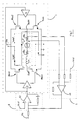
- Figure 3 is shown a circuit diagram used for the control of the current in a VCM in applications for hard - disk according to the present invention.
- a block 7 representing the circuitry for the speed recovery comprising a timing generator block 8 and a comparator 9, and also a switch S 1 can be seen suitable for selectively connecting a positive voltage, Vin+, or a negative voltage , Vin-.
- the block 7 receives two input signals, 10 and 11: the signal 10 is the output voltage of the amplifier A1 which is compared by means of the comparator 9 with two input thresholds Spd+ and Spd-. Said thresholds represent respectively the minimum speed at which the braking procedure is to be interrupted, in the case of clockwise and anti-clockwise rotation, respectively; the signal 11 is generated by a circuitry (not shown in the Figure) capable of signaling the loss of the supply voltage of the motor 2 to timing block 8 also called POR (Power On Reset).
- POR Power On Reset
- the comparator 9 is a window comparator having a double trip threshold and generates in output a first signal 12, representing the rotation direction of the motor 2, and a second signal 13, indicating that the motor 2 is turning beyond a determined speed.
- the time generator 8 receives said signals 11, 12 and 13 in input and generates a first signal 14, representing a braking period Tbrk, a second signal 15, representing an activation period Tact, and a third signal 16, representing the end of the speed recovery procedure.
- the last signal 16 is generated once the amplifier 9 detects that the speed of the VCM 2 has returned from the interval defined by the thresholds Spd- and Spd+, or that the speed has reached zero.
- the signal 15 commands the switch S1 for the period Tact in function of the rotation direction of the motor.
- S1 connects to the positive voltage Vin+ for all Tact if the rotation is clockwise while it connects to the negative voltage Vin- for all Tact if the rotation is anti-clockwise.
- the circuitry of the block 7 therefore detects the speed of VCM 2 at the time the supply is lost, for the whole duration of the braking procedure, and executes the generation of the periods Tbrk and Tact in such a manner as to command the bridge 1 turning on the diagonal of the output stage 1 in accordance with the direction that the current has to have to brake the motor, 2 duly commutating switch S1.
- motor 2 in the brake condition, that is when there is a loss of supply, if motor 2 is rotating at a certain speed, and is thus generating a BEMF, and therefore motor 2 is capable of pushing a current that opposes the motion immediately activating a braking step for a determined period Tbrk., higher is the speed reached by the motor before the loss of supply voltage, greater is the braking action during the brake functioning.
- the inventive system measures the BEMF generated by motor 2 by means of block 7.
- the system evaluates if motor 2 is rotating beyond a given speed and in which direction as it measures the voltage in output from amplifier A1, that is it measures the voltage present on line 10. This is possible because the current Ivcm is directly proportional to the BEMF, in accordance with the equation (2).
- the comparator 9 generates the signals 12 and 13, indicating respectively the rotation direction and if the speed of motor 2 is outside the interval Spd+ and Spd-, so that the timing block 8 generates the signal 15 so as to activate the diagonal of the output stage 1, for a predetermined period Tact, driving the current Ivcm in the correct direction to brake the motor 2, which current has the same direction but a greater value compared to the current present during the brake phase.
- the potential applied to the terminals of motor 2 is the sum of the voltage at the terminals of the output stage 1 and of the BEMF (BEMF generated by the motor in motion).
- an X-axis indicating the time, expressed in milliseconds, and a Y-axis indicating the current, expressed in milliamperes, can be seen.
- the instant t5 indicates the moment at which there is the loss of supply voltage and the signal 17 goes to zero thus activating block 7, period T5.
- the output stage 1 is placed in brake condition, in which the BEMF of the motor 2 pushes a braking current in the motor 2 itself for a period Tbrk.
- Tbrk the width and the direction of the current pushed by motor 2 are monitored by means of the double trip threshold comparator 9.
- the output stage 1 is driven saturating the two transistors MOS of the diagonal opposite that previously functioning for a period Tact.
- the comparator 9 In the event the braking procedure is required to be terminated with motor 2 stopped, the comparator 9 must be made with only one trip threshold Sref (not shown in the Figure) representing the motor stop condition, also called zero motion.
- Figure 5 shows a block diagram of the procedure for the speed recovery of a VCM according to the present invention.
- an initial block 40 can be noted followed by a first test block 18 on the signal 17 to check if said signal 17 is active or not. If negative, that is signal 17 active, branch 38, test 18 is again executed, while if positive, that is signal 17 equal to zero, branch 39, the brake condition is activated for a period Tbrk, block 19, that is there is a situation of loss of supply.
- test block 20 Successively a second test block 20 is executed to check if said period Tbrk has passed. If negative, branch 30, the test 20 is executed again while if affirmative, branch 29, the rotation speed of the VCM 2 is read, block 21, by means of the sense amplifier A1.
- branch 32 block 28 is executed so as to generate the signal 16 of end of procedure and to end the program, block 42.
- branch 33 block 24 is executed, that is switch S 1 is connected to the positive voltage Vin+ for a period Tact, while if the direction is anti-clockwise, branch 34, block 25 is executed, that is switch S 1 is connected to the negative voltage Vin- for a period Tact.
- Both blocks 24 and 25 activate a further block 26 so that the output stage 1 is driven saturating the two MOS of the diagonal of the output bridge 1 so as to force current in the same direction as the brake step.
- test 27 Successively a fifth test 27 is executed to check if the period Tact has passed. If negative, branch 36, test 27 is again executed, while if positive, branch 37, the cycle starts again from the brake condition 19.
- the periods Tbrk and Tact can be defined by the user so as to guarantee greater flexibility to the circuit and to the inventive method.
- One possible alternative embodiment is to carry out the control of the current during the step in which a diagonal of the output stage 1 is activated.
- the diagonal of the bridge 1 must be kept enabled until the current in motor 2 reaches a set value, after which it is completed and the step is carried out as previously illustrated.
Description
- The present invention refers to a circuit for the speed recovery of a direct current motor and method using said circuit, in particular for a Voice Coil Motor (VCM).
- A VCM is used for example to drive a mechanical arm on which the writing and/or reading heads for the data registered on a hard-disk are mounted.
- In said application field in the searching steps for new tracks to be written and/or read, the VCM is capable of giving strong accelerations/decelerations to the mechanical arm that supports the head so as to minimize the track search time.
- In fact during these phases the heads can reach a speed of the order of 2 ÷ 2.54 m/sec.
- A problem that has to be dealt with in a hard - disk, in the event that the supply voltage is suddenly cut off, is therefore to prevent the arm supporting the reading and writing heads from hitting at high speed against the stop positions inside and outside the platters forming the hard - disks.
- At present the speed recovery of the VCM has taken on a significant importance with the manufacturers of hard - disks, as the rotating speed they reach is very high and following the introduction of the ramp loading technique, a technique according to which the reading and/or writing heads are parked at the extremity of a ramp made of a plastic material outside the disks, it turns out to be essential for said arm, supporting the so-called heads, is prevented from hitting at high speed against said parking ramp.
- In the device L6244 produced by the Applicant, in the event of losing power, the output stage which drives the VCM is placed at high impedance so as to measure the speed of the motor through a value of the BEMF (Back Electromagnetic Force) generated by the same VCM. The value of the BEMF is memorized at the terminals of a capacity so that once, the sampling step of the BEMF is terminated, the braking action is executed by turning on the output stage again, that is by applying a voltage which has a value equal to that previously stored in the capacity but with an opposite sense so as to contrast the motion of the VCM. In this condition the capacity is unloaded through of a resistor, thus defining a time of duration of this speed recovery step.
- In another device L6246 produced by the Applicant, at the time the power supply is lost, the output stage driving the VCM is placed in the so-called brake configuration, that is in a configuration wherein the low side transistors of the output bridge are placed in conduction. In this manner it is as if the VCM had its terminals in short circuit and it is therefore the VCM itself that generates a braking current. This condition of brake is held for a time which is determined by the discharge constant of a R - C circuit.
- In both cases the speed recovery is executed in open loop and the motor is submitted to a braking action for a certain preset time, not keeping, however, the speed of the VCM itself under control.
- The effectiveness of these methods is technologically valid but is not sufficient to guarantee the speed recovery, in the time of a few milliseconds, which the modern VCMs are able to develop.
- Other systems known for braking the VCM, while keeping the control of the speed, drive the Pulse Width Modulation (PWM) type output stage in discontinuous mode. In this manner the braking current is interrupted and zeroed at every period of the PWM signal to permit the measurement of the BEMF and therefore the speed of the VCM itself, while permitting, however, to determine when the moment is for terminating the speed recovery procedure.
- In this case the effectiveness of the braking is not particularly energetic as the current must be zeroed periodically to be able to permit the measurement of the BEMF representing the speed of the VCM.
- In addition, for all the systems there is also the problem that in the absence of supply voltage the only circuitry which remains supplied is that which carries out the parking of the heads, while all the other devices, such as the micro-processor or the Digital Signal Processor (DSP), lose every functionality.
- US-A-6 140 784 discloses a circuit according to the pre-characterizing part of
claim 1. - In view of the state of the technique described, the object of the present invention is to make a circuit for the efficient and controlled recovery of the speed of a direct current VCM type motor, in particular at the time the power voltage is disconnected after a search for a new track to be read and/or written has been actuated.
- A further object of the present invention is to supply a method capable of guaranteeing the efficient and controlled recovery of the speed of a VCM.
- In accordance with the present invention, this object is reached through a circuit for recovering the speed of a direct current motor as defined in
claim 1. - In addition said object is reached by means of a method for the speed recovery of a direct current motor as defined in
claim 12. - Thanks to the present invention a circuit and a method can be provided which are capable of preventing the arm supporting the reading and/or writing heads from hitting at high speed against the end-of-stroke positions inside or outside the platters comprising the hard - disks.
- The characteristics and advantages of the present invention will become apparent from the following detailed description of an embodiment thereof, illustrated as non-limiting example in the enclosed drawings, in which:
- Figure 1 shows a circuit diagram used for the control of the current in a VCM in applications for hard - disk according to the known technique;
- Figure 2 shows the trend of the current profile at the terminals of the VCM during the speed recovery following a loss of supply in accordance with the diagram of Figure 1;
- Figure 3 shows a circuit diagram used for the control of the current in a VCM in applications for hard - disk according to the present invention;
- Figure 4 shows the trend of the current profile to the terminals of the VCM during the speed recovery following a loss of supply in accordance with the diagram of Figure 3;
- Figure 5 shows a block diagram of the procedure for the speed recovery of a VCM according to the present invention.
-
- In Figure 1 the circuit diagram is shown of a
control bridge 1 for a directcurrent motor 2 of VCM type, which motor is represented by the series of an inductor Lm, of a resistor Rm and of a generator of BEMF. -
Bridge 1 comprises a first couple of N-channel MOS type power transistors, MOS1 and MOS2, called high side transistors, and a second couple of N-channel MOS type power transistors, MOS3 and MOS4, called low side transistors. - The transistors MOS1 and MOS3 have respective gate electrodes controlled by a
first driver 3, in addition, the source electrode of the MOS1 is connected with the drain electrode of the MOS3, so as to make an ouput terminal OutP, the drain electrode of the MOS1 is connected to a supply terminal Vm and the source electrode of the MOS3 is grounded. - The transistors MOS2 and MOS4 have the respective gate electrodes controlled by a
second driver 4, in addition, the source electrode of the MOS2 is connected with the drain electrode of the MOS4, so as to make an output terminal OutM, the drain electrode of the MOS2 is connected to the supply terminal Vm and the source electrode of the MOS4 is grounded. - It can also be noted that between said output terminals OutP and OutM there are the
motor 2 VCM and a resistor Rs. - At the terminals of said resistor Rs a voltage is developed which is read by a
first block 5 comprising an operational amplifier A1, called sense amplifier. The amplifier A1 amplifies the voltage which develops at the terminals of Rs. Said amplifier A1 also has in input a reference voltage Vref which represents the working point of the whole current loop. On the basis of the result of said amplification and by means of asecond block 6, comprising another operational amplifier A2, called error amplifier, thebridge 1 is controlled by the inputs of thedrivers - Usually the
VCM 2 is driven by means of thebridge 1 functioning in class AB, and during the steps of searching for the tracks and of reading and/or writing, the movement of theVCM 2 is current controlled, in accordance with the diagram of Figure 1. - As known the best technique for the greatest effectiveness in the speed recovery following a search command is obtained by driving the output stage of 1 so as to activate the diagonal of the MOS transistors opposite to that which was activated in the acceleration step.
- Referring to the circuit of Figure 1, therefore, if for acceleration a current Ivcm1 (represented in the Figure with a continuous line) was supplied through the
transistors MOS 1 and MOS4, in order to obtain a more effective braking the diagonal of the control bridge has to be inverted activating the transistors MOS2 and MOS3 by driving a current Icvm2 in the opposite direction to the previous one (represented in the Figure with a dotted line). - In this manner the braking current Ivcm2, which is supplies by
VCM 2, depends on the contribution of the voltage Vm that supplies the output stage plus the contribution given by the generator of BEMF that the motor itself generates as it has the same polarity. - Such a technique presents the not unimportant problem of establishing for how long it is necessary to keep the configuration active so as to stop the
VCM 2 and to prevent it from accelerating in the opposite direction. - In Figure 2 the trend of the current profile at the terminals of the
VCM 2 is shown during the speed recovery following a supply loss in accordance with the diagram of Figure 1. - According to what is shown in said Figure, an X-axis indicating the time, expressed in milliseconds, and a Y-axis indicating the current, expressed in milliamperes, can be seen.
- In Figure 2 it can be seen that after a first period T1, that represents an acceleration step of the
VCM 2 during which the maximum voltage available is applied to themotor 2, at the instant t2 a loss of the supply voltage occurs and theoutput stage PWM 1 is placed in brake condition, that is both the low side transistors, MOS3 and MOS4, are turned on. - In this condition it is the
motor 2 that generates a braking action as shown during the second period T3. In fact, the BEMF generated by the speed of themotor 2 during the acceleration phase, period T1, is capable of pushing a current with such a direction to oppose the motion of the motor itself. - In Figure 3 is shown a circuit diagram used for the control of the current in a VCM in applications for hard - disk according to the present invention.
- Besides the circuit elements already illustrated in Figure 1, excluding the
block 6, ablock 7 representing the circuitry for the speed recovery , called speed recovery circuitry, can be noted, comprising atiming generator block 8 and acomparator 9, and also aswitch S 1 can be seen suitable for selectively connecting a positive voltage, Vin+, or a negative voltage , Vin-. - The
block 7 receives two input signals, 10 and 11: thesignal 10 is the output voltage of the amplifier A1 which is compared by means of thecomparator 9 with two input thresholds Spd+ and Spd-. Said thresholds represent respectively the minimum speed at which the braking procedure is to be interrupted, in the case of clockwise and anti-clockwise rotation, respectively; the signal 11 is generated by a circuitry (not shown in the Figure) capable of signaling the loss of the supply voltage of themotor 2 totiming block 8 also called POR (Power On Reset). - Thus the
comparator 9 is a window comparator having a double trip threshold and generates in output afirst signal 12, representing the rotation direction of themotor 2, and asecond signal 13, indicating that themotor 2 is turning beyond a determined speed. - The
time generator 8 receives saidsignals first signal 14, representing a braking period Tbrk, asecond signal 15, representing an activation period Tact, and athird signal 16, representing the end of the speed recovery procedure. - The
last signal 16 is generated once theamplifier 9 detects that the speed of theVCM 2 has returned from the interval defined by the thresholds Spd- and Spd+, or that the speed has reached zero. - The
signal 15 commands the switch S1 for the period Tact in function of the rotation direction of the motor. In fact S1 connects to the positive voltage Vin+ for all Tact if the rotation is clockwise while it connects to the negative voltage Vin- for all Tact if the rotation is anti-clockwise. - The circuitry of the
block 7 therefore detects the speed ofVCM 2 at the time the supply is lost, for the whole duration of the braking procedure, and executes the generation of the periods Tbrk and Tact in such a manner as to command thebridge 1 turning on the diagonal of theoutput stage 1 in accordance with the direction that the current has to have to brake the motor, 2 duly commutating switch S1. - Referring to Figure 3, when in brake condition, the current Ivcm (indicated with a continuous line arrow) that flows in the branch formed by the two low side MOS3 and MOS4, by
VCM 2 and by resistor Rs, is pushed by the BEMF generated bymotor 2 and therefore the equation in said branch is:motor 2, Rs is the detection resistor, RdsON is the channel resistance of transistor MOS in saturation, Ivcm is the current circulating inmotor 2 and Lm is the winding inductance ofmotor 2. - In the usual applications for hard - disk the resistance Rm is much greater than the sum of Rs and RdsON and the mechanical inertia of
motor 2 has a greater time constant than the electric constant and therefore during the brake step the equation (1) can be simplified as follows: - Therefore in the brake condition, that is when there is a loss of supply, if
motor 2 is rotating at a certain speed, and is thus generating a BEMF, and thereforemotor 2 is capable of pushing a current that opposes the motion immediately activating a braking step for a determined period Tbrk., higher is the speed reached by the motor before the loss of supply voltage, greater is the braking action during the brake functioning. - Therefore both in the case of loss of supply and with the motor functioning normally the inventive system measures the BEMF generated by
motor 2 by means ofblock 7. - In particular, during the brake condition, after the period Tbrk has passed, by means of the
comparator 9, the system evaluates ifmotor 2 is rotating beyond a given speed and in which direction as it measures the voltage in output from amplifier A1, that is it measures the voltage present online 10. This is possible because the current Ivcm is directly proportional to the BEMF, in accordance with the equation (2). - In accordance with this measurement the
comparator 9 generates thesignals motor 2 is outside the interval Spd+ and Spd-, so that thetiming block 8 generates thesignal 15 so as to activate the diagonal of theoutput stage 1, for a predetermined period Tact, driving the current Ivcm in the correct direction to brake themotor 2, which current has the same direction but a greater value compared to the current present during the brake phase. - In doing so we shall obtain that the potential applied to the terminals of
motor 2 is the sum of the voltage at the terminals of theoutput stage 1 and of the BEMF (BEMF generated by the motor in motion). - At the end of the period Tact, the
output stage 1 is again placed in brake condition and the cycle is repeated untilmotor 2 returns to the range Spd+ Spd-. - In Figure 4 the trend of the current profile to the terminals of the VCM is shown during the speed recovery following a loss of supply in accordance with the diagram of Figure 3.
- According to what is shown in said Figure an X-axis indicating the time, expressed in milliseconds, and a Y-axis indicating the current, expressed in milliamperes, can be seen.
- In said Figure 4 the time trend of a
signal 17 is represented, indicating that during the period T4, themotor 2 is supplied with the maximum voltage and therefore that it is in acceleration step and during the period T5 the loss of the supply voltage. - The instant t5 indicates the moment at which there is the loss of supply voltage and the
signal 17 goes to zero thus activatingblock 7, period T5. - In fact the
output stage 1 is placed in brake condition, in which the BEMF of themotor 2 pushes a braking current in themotor 2 itself for a period Tbrk. At the end of Tbrk the width and the direction of the current pushed bymotor 2 are monitored by means of the doubletrip threshold comparator 9. In function of the measurement made theoutput stage 1 is driven saturating the two transistors MOS of the diagonal opposite that previously functioning for a period Tact. - In this period Tact the voltage applied to
motor 2 is given by the supply voltage of the output stage Vm plus the contribution of the BEMF so as to rapidly increase the current circulating in themotor 2 thus increasing the braking action applied to themotor 2 itself. - At the end of the period Tact the brake condition is again activated for a new cycle Tbrk and Tact until the
motor 2 is slowed inside the threshold Spd+ Spd-. - Comparing Figure 2 and Figure 4 it can be deduced that the braking action made by means of
block 7 is more effective as the overall braking time T5 is lower than time T3. - In the event the braking procedure is required to be terminated with
motor 2 stopped, thecomparator 9 must be made with only one trip threshold Sref (not shown in the Figure) representing the motor stop condition, also called zero motion. - In fact at the end of the period Tact the brake condition is again activated for a new cycle Tbrk and Tact until the
motor 2 is fully stopped. - Figure 5 shows a block diagram of the procedure for the speed recovery of a VCM according to the present invention.
- According to what is illustrated in said Figure an
initial block 40 can be noted followed by afirst test block 18 on thesignal 17 to check if saidsignal 17 is active or not. If negative, that issignal 17 active,branch 38,test 18 is again executed, while if positive, that issignal 17 equal to zero,branch 39, the brake condition is activated for a period Tbrk, block 19, that is there is a situation of loss of supply. - Successively a
second test block 20 is executed to check if said period Tbrk has passed. If negative,branch 30, thetest 20 is executed again while if affirmative,branch 29, the rotation speed of theVCM 2 is read, block 21, by means of the sense amplifier A1. - Then there is a
third test block 22, to check if the speed of the VCM is between the assessment interval of thespeed detector 9. - If positive,
branch 32, block 28 is executed so as to generate thesignal 16 of end of procedure and to end the program, block 42. - If negative,
branch 31, afourth test 23 is executed to check which is the rotation direction ofmotor 2. - If the direction is clockwise,
branch 33, block 24 is executed, that isswitch S 1 is connected to the positive voltage Vin+ for a period Tact, while if the direction is anti-clockwise,branch 34, block 25 is executed, that isswitch S 1 is connected to the negative voltage Vin- for a period Tact. - Both blocks 24 and 25 activate a
further block 26 so that theoutput stage 1 is driven saturating the two MOS of the diagonal of theoutput bridge 1 so as to force current in the same direction as the brake step. - Successively a
fifth test 27 is executed to check if the period Tact has passed. If negative,branch 36,test 27 is again executed, while if positive,branch 37, the cycle starts again from thebrake condition 19. - The periods Tbrk and Tact can be defined by the user so as to guarantee greater flexibility to the circuit and to the inventive method.
- With the inventive system, therefore, more effective braking can be obtained and control on the speed of the motor during the braking phase can be obtained, as the
speed recovery circuitry 7 makes it possible to drive theoutput stage 1 combining the more energetic action, for a period Tact, which consists in unbalancing thebridge 1 so as to force the maximum braking current, with the brake action, for a period Tbrk, which consists in activating both the low side transistors MOS of thebridge 1. - One possible alternative embodiment is to carry out the control of the current during the step in which a diagonal of the
output stage 1 is activated. - In fact in the event the current is required to be controlled, the diagonal of the
bridge 1 must be kept enabled until the current inmotor 2 reaches a set value, after which it is completed and the step is carried out as previously illustrated.
Claims (12)
- Circuit for the speed recovery of a Voice Coil Motor, comprising: an output stage (1), including a first couple of transistors (MOS1, MOS2) and of a second couple of transistors (MOS3, MOS4), and detection means (5) for detecting a first current (Ivcm) circulating in said motor (2), characterized in that it comprises second means (7) for activating said second couple of transistors (MOS3, MOS4) of said output stage (1) for a first time period (Tbrk) so as to short-circuit said motor (2), and at the end of said first time period (Tbrk), said second means (7) being suitable for unbalancing said output stage (1) so as to force a second current (Ivcm), greater than said first current, for a determined second time period (Tact) according to the value detected by said detection means (5) during said first time period (Tbrk).
- Circuit for the speed recovery of a Voice Coil Motor according to claim 1, characterized in that said second means (7) comprise a comparator (9) for generating a direction signal (12) and a speed signal (13) and a timer (8) adapted to drive said output stage (1) for said first time period (Tbrk), to control a switch (S1) for said second time period (Tact) and to generate an end-of-procedure signal (16).
- Circuit for the speed recovery of a Voice Coil Motor according to claim 2, characterized in that said switch (S1) connects selectively said output stage (1) to a positive (Vin+) or negative (Vin-) voltage line for said second time period (Tact).
- Circuit for the speed recovery of a Voice Coil Motor according to claim 2, characterized in that said comparator (9) receives in input a couple of reference signals (Spd+, Spd-) and a signal generated (10) by said detection means (5) and generates in output a couple of signals (12, 13) suitable for indicating the exceeding of a determined rotation speed and rotation sense of said motor (2).
- Circuit for the speed recovery of a Voice Coil Motor according to claim 4, characterized in that said reference signals (Spd+, Spd-) represent the minimum speed at which said motor (2) is stopped.
- Circuit for the speed recovery of a Voice Coil Motor according to claim 4, characterized in that said reference signals (Spd+, Spd-) can be defined by the user.
- Circuit for the speed recovery of a Voice Coil Motor according to claim 4, characterized in that said comparator (9) receives in input one single reference signal (Sref) and said signal (10) generated by said detection means (5) and generates in output a couple of signals (12, 13) suitable for indicating the exceeding of a determined rotation speed and rotation sense of said motor (2).
- Circuit for the speed recovery of a Voice Coil Motor according to claim 2, characterized in that said timer (8) receives in input said two signals (12, 13) generated from said comparator (9) and a signal of loss of supply voltage (11) and said timer circuit (8) executes said first time period (Tbrk) and said second time period (Tact) as a function of said signals generated (12, 13) by said comparator (9).
- Circuit for the speed recovery of a Voice Coil Motor according to any of the previous claims, characterized in that said detection means (5) comprise a detection resistor (Rs) and an operational amplifier (A1).
- Circuit for the speed recovery of a Voice Coil Motor according to claim 9, characterized in that said operational amplifier (A1) receives the input voltage at the terminals of said detection resistor (Rs) and a voltage reference signal (Vref) so as to generate a signal (10) suitable for measuring the current that said motor (2) generates.
- Circuit for the speed recovery of a Voice Coil Motor according to any of the previous claims, characterized in that said output stage (1) is executed with N-channel MOSFET type power transistors (MOS1, MOS2, MOS3, MOS4) placed in AB configuration.
- Method for the speed recovery of a Voice Coil Motor
characterized in that it comprises the following succession of steps:a) checking whether there is a loss of supply voltage;b) short-circuiting for a first time period(Tbrk), a first couple of transistors (MOS3, MOS4);c) measuring a current (Ivcm) proportional to the rotation speed of said motor (2);d) measuring the polarity of said current (Ivcm), thereby determining the rotation direction of said motor (2);e) forcing a current (Ivcm) of greater intensity than that measured during steps (c) and (d) and with a same polarity, for a second time period (Tact) in said motor (2);f) repeating steps (b), (c), (d) and (e) until said current (Icvm) returns to a determined measure interval (Spd-; Spd+);g) generating an end-of-procedure signal (16).
Priority Applications (4)
| Application Number | Priority Date | Filing Date | Title |
|---|---|---|---|
| EP00830764A EP1207618B1 (en) | 2000-11-20 | 2000-11-20 | Circuit for the speed recovery of a direct current motor and method using said circuit |
| DE60023014T DE60023014D1 (en) | 2000-11-20 | 2000-11-20 | Circuit for recovering speed of a DC motor and method of using this circuit |
| US09/988,911 US6680598B2 (en) | 2000-11-20 | 2001-11-19 | Circuit for the speed recovery of a direct current motor and method using said circuit |
| JP2001354965A JP2002223588A (en) | 2000-11-20 | 2001-11-20 | Speed recovery circuit for dc current motor |
Applications Claiming Priority (1)
| Application Number | Priority Date | Filing Date | Title |
|---|---|---|---|
| EP00830764A EP1207618B1 (en) | 2000-11-20 | 2000-11-20 | Circuit for the speed recovery of a direct current motor and method using said circuit |
Publications (2)
| Publication Number | Publication Date |
|---|---|
| EP1207618A1 EP1207618A1 (en) | 2002-05-22 |
| EP1207618B1 true EP1207618B1 (en) | 2005-10-05 |
Family
ID=8175556
Family Applications (1)
| Application Number | Title | Priority Date | Filing Date |
|---|---|---|---|
| EP00830764A Expired - Lifetime EP1207618B1 (en) | 2000-11-20 | 2000-11-20 | Circuit for the speed recovery of a direct current motor and method using said circuit |
Country Status (4)
| Country | Link |
|---|---|
| US (1) | US6680598B2 (en) |
| EP (1) | EP1207618B1 (en) |
| JP (1) | JP2002223588A (en) |
| DE (1) | DE60023014D1 (en) |
Families Citing this family (11)
| Publication number | Priority date | Publication date | Assignee | Title |
|---|---|---|---|---|
| JP2003059216A (en) * | 2001-08-16 | 2003-02-28 | Internatl Business Mach Corp <Ibm> | Hard disk drive, data storage/reproducing device, head movement controller, and head movement control method |
| DE10226152A1 (en) * | 2002-06-13 | 2003-12-24 | Deere & Co | Circuit arrangement for operating a DC motor and adjusting device with such |
| KR100652436B1 (en) * | 2005-10-11 | 2006-12-01 | 삼성전자주식회사 | Method and apparatus of recording reference servo signal of hard disk drive |
| EP2050095B1 (en) * | 2006-04-10 | 2014-06-11 | Texas Instruments Incorporated | Differential voice coil motor control |
| TW200744304A (en) * | 2006-05-16 | 2007-12-01 | Wiz Energy Technology Company | Electronic brake and energy recycling system applied in brushless DC motor |
| CN101085602A (en) * | 2006-06-07 | 2007-12-12 | 宇泉能源科技股份有限公司 | Electric brake and energy recovery system for brushless DC motor |
| KR100734329B1 (en) * | 2006-07-24 | 2007-07-02 | 삼성전자주식회사 | Method to seek for servo pattern for servo pattern copy |
| TWI398090B (en) * | 2009-11-11 | 2013-06-01 | Princeton Technology Corp | Motor controlling circuit for multiple control modes |
| DE102010032335A1 (en) * | 2010-07-20 | 2012-01-26 | C. & E. Fein Gmbh | hand tool |
| JP6198447B2 (en) * | 2013-04-26 | 2017-09-20 | ローム株式会社 | Voice coil motor drive circuit, lens module and electronic device using the same |
| TWI571025B (en) * | 2016-01-21 | 2017-02-11 | 旺玖科技股份有限公司 | Negative voltage protection system |
Family Cites Families (19)
| Publication number | Priority date | Publication date | Assignee | Title |
|---|---|---|---|---|
| US3786329A (en) * | 1973-01-31 | 1974-01-15 | Kollmorgen Corp | Dynamic brake |
| JPS5620395U (en) * | 1979-07-23 | 1981-02-23 | ||
| US4545004A (en) * | 1984-03-22 | 1985-10-01 | General Motors Corporation | Bridge driver circuit for a DC electric motor |
| US5423192A (en) * | 1993-08-18 | 1995-06-13 | General Electric Company | Electronically commutated motor for driving a compressor |
| JPH062316U (en) * | 1992-06-12 | 1994-01-14 | 株式会社ニコン | Motor drive device used for camera and its accessories |
| KR100295029B1 (en) * | 1992-11-17 | 2001-10-24 | 요트.게.아. 롤페즈 | Motor driving circuit |
| JP3545049B2 (en) * | 1993-06-22 | 2004-07-21 | エスティーマイクロエレクトロニクス,インコーポレイテッド | Back electromotive force rectified voltage at power supply energy failure |
| DE69427292D1 (en) * | 1994-07-19 | 2001-06-28 | Sgs Thomson Microelectronics | Bi-directional current sensing circuit for an H-bridge |
| US5631527A (en) * | 1994-09-06 | 1997-05-20 | Sgs-Thomson Microelectronics, Inc. | Voice coil motor feedback control circuit |
| JPH098566A (en) * | 1995-06-06 | 1997-01-10 | Sgs Thomson Microelectron Inc | Amplifier output stage |
| JPH0923688A (en) * | 1995-06-29 | 1997-01-21 | Sgs Thomson Microelectron Inc | Power-down braking latch for brushless dc motor |
| US5737144A (en) * | 1996-06-05 | 1998-04-07 | Quantum Corporation | Switched boost voltage generator for actuator retract in disk drive |
| JP3114800B2 (en) * | 1997-06-30 | 2000-12-04 | 日本電気株式会社 | Motor drive circuit |
| EP0911954B1 (en) * | 1997-10-23 | 2001-05-02 | STMicroelectronics S.r.l. | PWM drive system in a current mode. |
| US6160368A (en) * | 1998-06-22 | 2000-12-12 | Western Digital Corporation | Faster spin-down operation in a disk drive by utilizing pulsed braking |
| US6229273B1 (en) * | 1999-02-23 | 2001-05-08 | Lucent Technologies, Inc. | Actuator driver circuit |
| US6140784A (en) * | 1999-06-09 | 2000-10-31 | Quantum Corporation | Power off velocity control for disk drives |
| US6369534B1 (en) * | 2000-04-26 | 2002-04-09 | Stmicroelectronics, Inc. | Circuit and method for detecting backward spin of a spindle motor for a disk drive |
| US6353298B1 (en) * | 2001-04-11 | 2002-03-05 | Texas Instruments Incorporated | Low distortion audio range class-AB full H-bridge pre-driver amplifier |
-
2000
- 2000-11-20 DE DE60023014T patent/DE60023014D1/en not_active Expired - Lifetime
- 2000-11-20 EP EP00830764A patent/EP1207618B1/en not_active Expired - Lifetime
-
2001
- 2001-11-19 US US09/988,911 patent/US6680598B2/en not_active Expired - Lifetime
- 2001-11-20 JP JP2001354965A patent/JP2002223588A/en active Pending
Also Published As
| Publication number | Publication date |
|---|---|
| JP2002223588A (en) | 2002-08-09 |
| EP1207618A1 (en) | 2002-05-22 |
| DE60023014D1 (en) | 2005-11-10 |
| US6680598B2 (en) | 2004-01-20 |
| US20020081106A1 (en) | 2002-06-27 |
Similar Documents
| Publication | Publication Date | Title |
|---|---|---|
| EP1207618B1 (en) | Circuit for the speed recovery of a direct current motor and method using said circuit | |
| US20060181237A1 (en) | Method of stall detection for stepper motor system | |
| US20220090431A1 (en) | Open/close control device, open/close control system, open/close control method, and program | |
| JP4077889B2 (en) | DC motor overcurrent detection device | |
| EP1118994A2 (en) | Method and apparatus for ramp loading in a hard disk drive | |
| EP1107444A3 (en) | Motor and disk drive apparatus | |
| CN110492581B (en) | Recovering energy from a spindle motor in response to an external power failure | |
| JP3578568B2 (en) | Power window control device for vehicles | |
| JP4811859B2 (en) | Magnetic disk control method and magnetic disk control apparatus | |
| JP4652610B2 (en) | Step motor rotation control device | |
| JPS59177767A (en) | Access control circuit | |
| JP2010035312A (en) | Dc motor controller | |
| JPH04222970A (en) | Head positioning control system for magnetic disk device | |
| JP2002174075A (en) | Opening and closing controller | |
| JPS5899276A (en) | Brake device for motor | |
| JP2002199791A (en) | Current detection circuit and motor controller provided therewith | |
| CN106208843B (en) | Motor drive circuit, vibration device, and electronic apparatus | |
| JPS58163280A (en) | Damping circuit for direct drive type motor | |
| JP2000087645A (en) | Power window device | |
| JP2551836B2 (en) | Drive controller | |
| EP0426447A2 (en) | Track jump control circuit | |
| JPH0440793B2 (en) | ||
| EP1777141A1 (en) | System and method for determining operational states of first and second electrical contacts in a motor | |
| JPH11126412A (en) | Rotation type storage device | |
| JP2915918B2 (en) | Variable element destruction prevention circuit |
Legal Events
| Date | Code | Title | Description |
|---|---|---|---|
| PUAI | Public reference made under article 153(3) epc to a published international application that has entered the european phase |
Free format text: ORIGINAL CODE: 0009012 |
|
| AX | Request for extension of the european patent |
Free format text: AL;LT;LV;MK;RO;SI |
|
| 17P | Request for examination filed |
Effective date: 20021113 |
|
| AKX | Designation fees paid |
Designated state(s): DE FR GB IT |
|
| 17Q | First examination report despatched |
Effective date: 20040616 |
|
| GRAP | Despatch of communication of intention to grant a patent |
Free format text: ORIGINAL CODE: EPIDOSNIGR1 |
|
| GRAS | Grant fee paid |
Free format text: ORIGINAL CODE: EPIDOSNIGR3 |
|
| GRAA | (expected) grant |
Free format text: ORIGINAL CODE: 0009210 |
|
| AK | Designated contracting states |
Kind code of ref document: B1 Designated state(s): DE FR GB IT |
|
| REG | Reference to a national code |
Ref country code: GB Ref legal event code: FG4D |
|
| REF | Corresponds to: |
Ref document number: 60023014 Country of ref document: DE Date of ref document: 20051110 Kind code of ref document: P |
|
| PG25 | Lapsed in a contracting state [announced via postgrant information from national office to epo] |
Ref country code: DE Free format text: LAPSE BECAUSE OF FAILURE TO SUBMIT A TRANSLATION OF THE DESCRIPTION OR TO PAY THE FEE WITHIN THE PRESCRIBED TIME-LIMIT Effective date: 20060106 |
|
| PLBE | No opposition filed within time limit |
Free format text: ORIGINAL CODE: 0009261 |
|
| STAA | Information on the status of an ep patent application or granted ep patent |
Free format text: STATUS: NO OPPOSITION FILED WITHIN TIME LIMIT |
|
| 26N | No opposition filed |
Effective date: 20060706 |
|
| PG25 | Lapsed in a contracting state [announced via postgrant information from national office to epo] |
Ref country code: FR Free format text: LAPSE BECAUSE OF FAILURE TO SUBMIT A TRANSLATION OF THE DESCRIPTION OR TO PAY THE FEE WITHIN THE PRESCRIBED TIME-LIMIT Effective date: 20061020 |
|
| EN | Fr: translation not filed | ||
| PGFP | Annual fee paid to national office [announced via postgrant information from national office to epo] |
Ref country code: IT Payment date: 20071117 Year of fee payment: 8 |
|
| PG25 | Lapsed in a contracting state [announced via postgrant information from national office to epo] |
Ref country code: FR Free format text: LAPSE BECAUSE OF FAILURE TO SUBMIT A TRANSLATION OF THE DESCRIPTION OR TO PAY THE FEE WITHIN THE PRESCRIBED TIME-LIMIT Effective date: 20051130 |
|
| PG25 | Lapsed in a contracting state [announced via postgrant information from national office to epo] |
Ref country code: FR Free format text: LAPSE BECAUSE OF FAILURE TO SUBMIT A TRANSLATION OF THE DESCRIPTION OR TO PAY THE FEE WITHIN THE PRESCRIBED TIME-LIMIT Effective date: 20051005 |
|
| PG25 | Lapsed in a contracting state [announced via postgrant information from national office to epo] |
Ref country code: IT Free format text: LAPSE BECAUSE OF NON-PAYMENT OF DUE FEES Effective date: 20081120 |
|
| PGFP | Annual fee paid to national office [announced via postgrant information from national office to epo] |
Ref country code: GB Payment date: 20101026 Year of fee payment: 11 |
|
| GBPC | Gb: european patent ceased through non-payment of renewal fee |
Effective date: 20121120 |
|
| PG25 | Lapsed in a contracting state [announced via postgrant information from national office to epo] |
Ref country code: GB Free format text: LAPSE BECAUSE OF NON-PAYMENT OF DUE FEES Effective date: 20121120 |