WO2014162979A1 - 光電変換装置 - Google Patents
光電変換装置 Download PDFInfo
- Publication number
- WO2014162979A1 WO2014162979A1 PCT/JP2014/058888 JP2014058888W WO2014162979A1 WO 2014162979 A1 WO2014162979 A1 WO 2014162979A1 JP 2014058888 W JP2014058888 W JP 2014058888W WO 2014162979 A1 WO2014162979 A1 WO 2014162979A1
- Authority
- WO
- WIPO (PCT)
- Prior art keywords
- type
- thin film
- amorphous thin
- silicon substrate
- photoelectric conversion
- Prior art date
- Legal status (The legal status is an assumption and is not a legal conclusion. Google has not performed a legal analysis and makes no representation as to the accuracy of the status listed.)
- Ceased
Links
Images

















Classifications
-
- H—ELECTRICITY
- H10—SEMICONDUCTOR DEVICES; ELECTRIC SOLID-STATE DEVICES NOT OTHERWISE PROVIDED FOR
- H10F—INORGANIC SEMICONDUCTOR DEVICES SENSITIVE TO INFRARED RADIATION, LIGHT, ELECTROMAGNETIC RADIATION OF SHORTER WAVELENGTH OR CORPUSCULAR RADIATION
- H10F10/00—Individual photovoltaic cells, e.g. solar cells
- H10F10/10—Individual photovoltaic cells, e.g. solar cells having potential barriers
- H10F10/16—Photovoltaic cells having only PN heterojunction potential barriers
- H10F10/164—Photovoltaic cells having only PN heterojunction potential barriers comprising heterojunctions with Group IV materials, e.g. ITO/Si or GaAs/SiGe photovoltaic cells
- H10F10/165—Photovoltaic cells having only PN heterojunction potential barriers comprising heterojunctions with Group IV materials, e.g. ITO/Si or GaAs/SiGe photovoltaic cells the heterojunctions being Group IV-IV heterojunctions, e.g. Si/Ge, SiGe/Si or Si/SiC photovoltaic cells
- H10F10/166—Photovoltaic cells having only PN heterojunction potential barriers comprising heterojunctions with Group IV materials, e.g. ITO/Si or GaAs/SiGe photovoltaic cells the heterojunctions being Group IV-IV heterojunctions, e.g. Si/Ge, SiGe/Si or Si/SiC photovoltaic cells the Group IV-IV heterojunctions being heterojunctions of crystalline and amorphous materials, e.g. silicon heterojunction [SHJ] photovoltaic cells
-
- H—ELECTRICITY
- H10—SEMICONDUCTOR DEVICES; ELECTRIC SOLID-STATE DEVICES NOT OTHERWISE PROVIDED FOR
- H10F—INORGANIC SEMICONDUCTOR DEVICES SENSITIVE TO INFRARED RADIATION, LIGHT, ELECTROMAGNETIC RADIATION OF SHORTER WAVELENGTH OR CORPUSCULAR RADIATION
- H10F77/00—Constructional details of devices covered by this subclass
- H10F77/70—Surface textures, e.g. pyramid structures
- H10F77/703—Surface textures, e.g. pyramid structures of the semiconductor bodies, e.g. textured active layers
-
- Y—GENERAL TAGGING OF NEW TECHNOLOGICAL DEVELOPMENTS; GENERAL TAGGING OF CROSS-SECTIONAL TECHNOLOGIES SPANNING OVER SEVERAL SECTIONS OF THE IPC; TECHNICAL SUBJECTS COVERED BY FORMER USPC CROSS-REFERENCE ART COLLECTIONS [XRACs] AND DIGESTS
- Y02—TECHNOLOGIES OR APPLICATIONS FOR MITIGATION OR ADAPTATION AGAINST CLIMATE CHANGE
- Y02E—REDUCTION OF GREENHOUSE GAS [GHG] EMISSIONS, RELATED TO ENERGY GENERATION, TRANSMISSION OR DISTRIBUTION
- Y02E10/00—Energy generation through renewable energy sources
- Y02E10/50—Photovoltaic [PV] energy
Definitions
- the present invention relates to a photoelectric conversion device.
- Patent Documents 1 and 2 Conventionally, a photoelectric conversion device in which two concavo-convex structures having different concavo-convex sizes are provided on the light incident side is known (Patent Documents 1 and 2).
- a crystalline silicon substrate has a first uneven structure and a second uneven structure formed on the surface of the first uneven structure.
- the second uneven structure has an uneven size smaller than that of the first uneven structure. Thereby, the reflectance at the light incident side is lowered.
- a crystalline silicon solar cell is formed on a surface of a light incident side of a crystalline silicon substrate having a first concavo-convex structure on a surface on the light incident side, and a second concavo-convex structure.
- the second uneven structure has an uneven size smaller than that of the first uneven structure.
- Patent Document 1 since the crystalline silicon substrate has two uneven structures on the surface on the light incident side, there is a problem that the contact area between the crystalline silicon substrate and the electrode becomes large and carrier recombination is likely to occur. is there.
- Patent Document 2 since the crystalline silicon substrate has a concavo-convex structure on the surface on the light incident side, there is a problem that the contact area between the crystalline silicon substrate and the transparent conductive film is large, and carrier recombination is likely to occur. .
- the present invention has been made to solve such a problem, and an object thereof is to provide a photoelectric conversion device capable of reducing the reflectance on the light incident side and reducing the recombination of carriers. It is.
- a photoelectric conversion device is a photoelectric conversion device that converts light into electricity, and includes a crystalline silicon substrate and an amorphous thin film.
- a first uneven structure having a first uneven size is provided on the surface on the light incident side.
- the amorphous thin film has a second concavo-convex structure having a second concavo-convex size different from the first concavo-convex size provided on the surface on the light incident side and is in contact with the light incident side surface of the crystal silicon substrate It is provided above and contains a group IV element.
- the first uneven size is smaller than the second uneven size in the photoelectric conversion device according to the embodiment of the present invention.
- the first uneven size is larger than the second uneven size in the photoelectric conversion device according to the embodiment of the present invention.
- the photoelectric conversion device is the photoelectric conversion device according to any one of (1) to (3), wherein the amorphous thin film is the first amorphous It consists of either a thin film or a second amorphous thin film.
- the first amorphous thin film is provided on the crystalline silicon substrate in contact with the surface on the light incident side of the crystalline silicon substrate and has a conductivity type opposite to that of the crystalline silicon substrate.
- the structure is composed of a first amorphous layer provided on the surface on the light incident side.
- the second amorphous thin film is provided on the crystalline silicon substrate in contact with the surface on the light incident side of the crystalline silicon substrate, and includes a second amorphous layer having an i-type conductivity type, A second conductive layer is provided on the second amorphous layer in contact with the amorphous layer and has a conductivity type opposite to that of the crystalline silicon substrate, and the second concavo-convex structure is provided on the light incident side surface. 3 amorphous layers.
- the photoelectric conversion device according to the embodiment of the present invention is the photoelectric conversion device according to (4), wherein the crystalline silicon substrate has an n-type conductivity type, and the first amorphous layer Is made of p-type amorphous silicon, the second amorphous layer is made of i-type amorphous silicon, and the third amorphous layer is made of p-type amorphous silicon.
- the photoelectric conversion device according to the embodiment of the present invention is the photoelectric conversion device according to (4), wherein the crystalline silicon substrate has a p-type conductivity type, and the first amorphous The layer is made of n-type amorphous silicon, the second amorphous layer is made of i-type amorphous silicon, and the third amorphous layer is made of n-type amorphous silicon.
- the photoelectric conversion device according to the embodiment of the present invention further includes an electrode arranged on the light incident side in the photoelectric conversion device according to any one of (4) to (6), Of the surface on the light incident side of the crystalline silicon substrate, the portion facing the electrode is flat.
- the photoelectric conversion device according to the embodiment of the present invention is the photoelectric conversion device according to any one of (1) to (3), wherein the crystalline silicon substrate includes a bulk region and a light incident side. And a diffusion region having a conductivity type opposite to that of the bulk region.
- the photoelectric conversion device according to the embodiment of the present invention further includes an electrode provided in contact with a part of the diffusion region of the crystalline silicon substrate in the photoelectric conversion device according to (8), A part of the diffusion region is a flat plane.
- the photoelectric conversion device according to the embodiment of the present invention is the photoelectric conversion device according to any one of (1) to (9), wherein the crystalline silicon substrate is a single crystal silicon substrate or a polycrystalline It consists of a silicon substrate.
- the photoelectric conversion device in the photoelectric conversion device according to any one of (1) to (3), includes a plurality of first amorphous thin films and a plurality of first amorphous thin films. And a second amorphous thin film.
- the plurality of first amorphous thin films are provided on the side opposite to the light incident side of the crystalline silicon substrate and have a conductivity type opposite to that of the crystalline silicon substrate.
- the plurality of second amorphous thin films are provided on the opposite side to the light incident side of the crystalline silicon substrate and have the same conductivity type as that of the crystalline silicon substrate, and the plurality of second amorphous thin films are in the in-plane direction of the crystalline silicon substrate. Alternatingly arranged with one amorphous thin film.
- the crystalline silicon substrate is a single crystal silicon substrate.
- the photoelectric conversion device according to the embodiment of the present invention includes a plurality of first amorphous thin films and a plurality of second amorphous thin films, A third amorphous film having an i-type conductivity type and provided in contact with the plurality of first amorphous thin films, the plurality of second amorphous thin films, and the single crystal silicon substrate between the single crystal silicon substrate A thin film is further provided.
- the photoelectric conversion device according to the embodiment of the present invention is the photoelectric conversion device according to (12), wherein the first amorphous thin film has a single-crystal silicon substrate having an n-type conductivity type.
- the second amorphous thin film is made of an n-type single crystal silicon substrate.
- the third amorphous thin film is made of i-type. Made of amorphous silicon.
- the photoelectric conversion device according to the embodiment of the present invention is the photoelectric conversion device according to any one of (1) to (3), wherein the crystalline silicon substrate includes a plurality of first diffusion regions. And a plurality of second diffusion regions.
- the plurality of first diffusion regions are provided in contact with a bulk region made of single crystal silicon and a back surface made of single crystal silicon and opposite to the light incident side of the crystal silicon substrate, opposite to the conductivity type of the bulk region. Has conductivity type.
- the plurality of second diffusion regions are made of single crystal silicon and have the same conductivity type as that of the bulk region, and are in contact with the back surface alternately with the plurality of first diffusion regions in the in-plane direction of the crystalline silicon substrate. Be placed.
- the amorphous thin film is the first amorphous It consists of a thin film, a second amorphous thin film, a third amorphous thin film, a fourth amorphous thin film, or a fifth amorphous thin film.
- the first amorphous thin film is provided in contact with the surface on the light incident side of the crystalline silicon substrate, and the second concavo-convex structure is provided on the surface on the light incident side. It consists of a crystalline layer.
- the second amorphous thin film is provided in contact with the surface on the light incident side of the crystalline silicon substrate, and the second uneven structure is provided on the surface on the light incident side. It consists of a crystalline layer.
- the third amorphous thin film is provided in contact with the surface on the light incident side of the crystalline silicon substrate, the second uneven structure is provided on the surface on the light incident side, and has a p-type conductivity type. It consists of a crystalline layer.
- the fourth amorphous thin film is provided in contact with the surface on the light incident side of the crystalline silicon substrate, and is formed on the fourth amorphous layer having the i-type conductivity type and the fourth amorphous layer.
- the second concavo-convex structure is provided on the surface on the light incident side and is formed of a fifth amorphous layer having an n-type conductivity type.
- the fifth amorphous thin film is provided in contact with the surface on the light incident side of the crystalline silicon substrate, and is formed on the sixth amorphous layer having the i-type conductivity type and the sixth amorphous layer.
- the second uneven structure is provided on the surface on the light incident side, and is formed of a seventh amorphous layer having a p-type conductivity type.
- the photoelectric conversion device according to the embodiment of the present invention is the photoelectric conversion device according to (15), wherein each of the first, fourth, and sixth amorphous layers is an i-type amorphous material.
- Each of the second and fifth amorphous layers is made of n-type amorphous silicon, and each of the third and seventh amorphous layers is made of p-type amorphous silicon. .
- two concavo-convex structures having different concavo-convex sizes are arranged on the light incident side, and the surface on the light incident side of the crystalline silicon substrate is formed by an amorphous thin film containing a group IV element. Covered. As a result, incident light is scattered by the two concavo-convex structures and enters the crystalline silicon substrate. The surface of the crystalline silicon substrate on the light incident side is passivated by an amorphous thin film.
- the reflectance on the light incident side can be reduced, and the recombination of carriers at the interface between the amorphous thin film and the crystalline silicon substrate can be reduced.
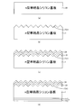
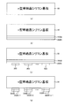
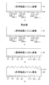
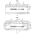
- FIG. 2 is an enlarged view in which a part of an n-type single crystal silicon substrate and an amorphous thin film shown in FIG. 1 are enlarged. It is the schematic which shows the structure of the amorphous thin film shown in FIG. It is a 1st process drawing which shows the manufacturing method of the photoelectric conversion apparatus shown in FIG.
- FIG. 4 is a second process diagram illustrating a method for manufacturing the photoelectric conversion device illustrated in FIG. 1.
- FIG. 4 is a third process diagram illustrating a method for manufacturing the photoelectric conversion device illustrated in FIG. 1.
- FIG. 3 is a schematic diagram illustrating a configuration of another photoelectric conversion device according to Embodiment 1.
- FIG. 8 is a first process diagram illustrating a method for manufacturing the photoelectric conversion device illustrated in FIG. 7.
- FIG. 8 is a second process diagram illustrating a method for manufacturing the photoelectric conversion device illustrated in FIG. 7.
- FIG. 8 is a third process diagram illustrating the method for manufacturing the photoelectric conversion device illustrated in FIG. 7.
- FIG. 5 is a schematic diagram illustrating a configuration of still another photoelectric conversion device according to Embodiment 1.
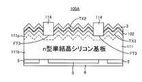
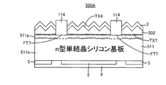
- FIG. 5 is a schematic diagram illustrating a configuration of a photoelectric conversion apparatus according to a second embodiment. It is the schematic which shows the structure of the amorphous thin film shown in FIG. FIG.
- FIG. 14 is a first process diagram showing a method of manufacturing the photoelectric conversion device shown in FIG. 13.
- FIG. 14 is a second process diagram illustrating a method of manufacturing the photoelectric conversion device illustrated in FIG. 13.
- FIG. 14 is a third process diagram illustrating a method for manufacturing the photoelectric conversion device illustrated in FIG. 13.
- 6 is a schematic diagram illustrating a configuration of another photoelectric conversion device according to Embodiment 2.
- FIG. FIG. 6 is a schematic diagram illustrating a configuration of a photoelectric conversion device according to a third embodiment. It is the schematic which shows the structure of the amorphous thin film shown in FIG.
- FIG. 20 is a schematic view showing a configuration of another amorphous thin film shown in FIG. 19.
- FIG. 20 is a schematic view showing a configuration of another amorphous thin film shown in FIG. 19.
- FIG. 20 is a first process diagram illustrating a method of manufacturing the photoelectric conversion device illustrated in FIG. 19.
- FIG. 20 is a second process diagram illustrating the method of manufacturing the photoelectric conversion device illustrated in FIG. 19.
- FIG. 20 is a third process diagram illustrating the method of manufacturing the photoelectric conversion device illustrated in FIG. 19.
- FIG. 20 is a fourth process diagram illustrating the method of manufacturing the photoelectric conversion device illustrated in FIG. 19.
- FIG. 6 is a schematic diagram illustrating a configuration of a photoelectric conversion apparatus according to a fourth embodiment.
- FIG. 27 is a first process diagram illustrating a method of manufacturing the photoelectric conversion device illustrated in FIG. 26.
- FIG. 27 is a second process diagram illustrating the method of manufacturing the photoelectric conversion device illustrated in FIG. 26.
- FIG. 27 is a third process diagram illustrating the method of manufacturing the photoelectric conversion device illustrated in FIG. 26.
- FIG. 27 is a fourth process diagram illustrating the method of manufacturing the photoelectric conversion device illustrated in FIG. 26.
- FIG. 6 is a schematic diagram illustrating a configuration of a photoelectric conversion apparatus according to a fifth embodiment.
- FIG. 10 is a schematic diagram illustrating a configuration of another photoelectric conversion device according to Embodiment 5.
- FIG. 10 is a schematic diagram illustrating a configuration of a photoelectric conversion apparatus according to a sixth embodiment.
- FIG. 10 is a schematic diagram illustrating a configuration of another photoelectric conversion device according to Embodiment 6.
- FIG. 10 is a schematic diagram illustrating a configuration of a photoelectric conversion apparatus according to a seventh embodiment.
- FIG. 10 is a schematic diagram illustrating a configuration of a photoelectric conversion apparatus according to a seventh embodiment.
- FIG. 10 is a schematic diagram illustrating a configuration of a photoelectric conversion apparatus according to an eighth embodiment. It is the schematic which shows the structure of a photoelectric conversion module provided with the photoelectric conversion apparatus by this embodiment. It is the schematic which shows the structure of a solar energy power generation system provided with the photoelectric conversion apparatus by this embodiment. It is the schematic which shows the structure of the photoelectric conversion module array shown in FIG. It is the schematic which shows the structure of another photovoltaic power generation system provided with the photoelectric conversion apparatus by this embodiment. It is the schematic which shows the structure of another photovoltaic power generation system provided with the photoelectric conversion apparatus by this embodiment. It is the schematic which shows the structure of another solar power generation system provided with the photoelectric conversion apparatus by this embodiment.
- amorphous means that the ratio of the peak intensity based on crystals to the peak intensity based on amorphous in Raman scattering is 0.1 or less.
- amorphous silicon is expressed as “a-Si”, this notation actually means that a hydrogen (H) atom is included.
- FIG. 1 is a schematic diagram showing a configuration of a photoelectric conversion apparatus according to Embodiment 1 of the present invention.
- a photoelectric conversion device 10 according to Embodiment 1 of the present invention includes an n-type single crystal silicon substrate 1, an amorphous thin film 2, a transparent conductive film 3, electrodes 4 and 6, and passivation. And a membrane 5.
- the n-type single crystal silicon substrate 1 has a specific resistance of 0.1 to 10 ⁇ cm and a thickness of 100 to 300 ⁇ m.
- the n-type single crystal silicon substrate 1 has a (100) plane orientation.
- the n-type single crystal silicon substrate 1 has a concavo-convex structure TX1 on the surface on the light incident side.
- the amorphous thin film 2 is disposed on the n-type single crystal silicon substrate 1 in contact with the light incident side surface of the n-type single crystal silicon substrate 1.
- the amorphous thin film 2 has a concavo-convex structure TX2 on the light incident side surface.
- the transparent conductive film 3 is disposed on the amorphous thin film 2 in contact with the amorphous thin film 2.
- the transparent conductive film 3 is made of ITO (Indium Tin Oxide), SnO 2 , ZnO, or the like.
- the electrodes 4 are in contact with the transparent conductive film 3 and are arranged on the transparent conductive film 3 at a desired interval.
- the electrode 4 is made of, for example, silver (Ag).
- the passivation film 5 is made of, for example, silicon oxide (SiO 2 ) and has a thickness of 100 nm to 200 nm.
- the electrode 6 is disposed in contact with the back surface of the n-type single crystal silicon substrate 1 and the passivation film 5.
- the electrode 6 is made of, for example, aluminum (Al).
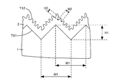
- FIG. 2 is an enlarged view of a part of the n-type single crystal silicon substrate 1 and the amorphous thin film 2 shown in FIG.
- the height H1 is defined as the distance between the valley and the mountain
- the width W1 is defined as the distance between two adjacent valleys or the distance between two adjacent mountains.
- the height H2 and the width W2 are defined.
- the height H1 is, for example, 1 ⁇ m to 10 ⁇ m, and the width W1 is 1 ⁇ m to 10 ⁇ m.
- the height H2 is, for example, 1 nm to 200 nm, and the width W2 is 1 nm to 200 nm.
- the uneven size of the uneven structure TX1 is defined by the height H1 and / or the width W1. The same applies to the uneven structure TX2.
- the concavo-convex structure TX1 has a larger concavo-convex size than the concavo-convex structure TX2.
- the photoelectric conversion device 10 is provided with the concavo-convex structure TX1 on the light incident side surface of the n-type single crystal silicon substrate 1, and the concavo-convex structure TX2 having a concavo-convex size smaller than the concavo-convex structure TX1 is more incident than the concavo-convex structure TX1 It is provided on the side.
- the incident light is scattered by the concavo-convex structure TX2, and the scattered light is further scattered by the concavo-convex structure TX1. Therefore, the reflectance of incident light can be reduced as compared with the case where only one uneven structure is provided on the light incident side of the photoelectric conversion device 10.
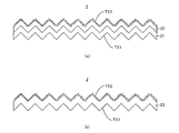
- FIG. 3 is a schematic view showing the configuration of the amorphous thin film 2 shown in FIG.
- amorphous thin film 2 includes an i-type amorphous thin film 21 and a p-type amorphous thin film 22 (see (a)).
- the i-type amorphous thin film 21 is arranged along the uneven structure TX1 on the light incident side of the n-type single crystal silicon substrate 1.
- the p-type amorphous thin film 22 is disposed on the i-type amorphous thin film 21 in contact with the i-type amorphous thin film 21, and has a concavo-convex structure TX2 on the light incident side surface.
- the i-type amorphous thin film 21 includes i-type amorphous silicon (i-type a-Si), i-type amorphous silicon germanium (i-type a-SiGe), i-type amorphous germanium (i-type a-Ge).
- I-type amorphous silicon carbide i-type a-SiC
- i-type amorphous silicon nitride i-type a-SiN
- i-type amorphous silicon oxide i-type a-SiO
- It is made of any one of amorphous silicon carbon oxide (i-type a-SiCO) or the like, and is generally made of an i-type amorphous thin film containing a group IV element.
- the i-type amorphous thin film 21 has a thickness of 10 to 20 nm.
- the p-type amorphous thin film 22 includes p-type amorphous silicon (p-type a-Si), p-type amorphous silicon germanium (p-type a-SiGe), and p-type amorphous germanium (p-type a-Ge).
- p-type amorphous silicon carbide p-type a-SiC
- p-type amorphous silicon nitride p-type a-SiN
- p-type amorphous silicon oxide p-type a-SiO
- It is made of any one of amorphous silicon carbon oxide (p-type a-SiCO) or the like, and is generally made of a p-type amorphous thin film containing a group IV element.
- the p-type amorphous thin film 22 has a thickness of 1 to 200 nm.
- the p-type amorphous thin film 22 includes, for example, boron (B) as a p-type dopant, and the concentration of B is, for example, 1 ⁇ 10 18 cm ⁇ 3 to 1 ⁇ 10 19 cm ⁇ 3 .
- the combination of the material of the i-type amorphous thin film 21 and the material of the p-type amorphous thin film 22 is arbitrary, but the i-type amorphous thin film 21 is made of i-type a-Si, and the p-type amorphous A combination in which the thin film 22 is made of p-type a-Si is preferable.
- the amorphous thin film 2 may be composed of a p-type amorphous thin film 23 (see FIG. 3B).
- the p-type amorphous thin film 23 is disposed along the light incident side concavo-convex structure TX1 of the n-type single crystal silicon substrate 1, and has a concavo-convex structure TX2 on the light incident side surface.
- the p-type amorphous thin film 23 is made of the same material as the p-type amorphous thin film 22 described above, and contains B having a concentration of 1 ⁇ 10 17 cm ⁇ 3 to 1 ⁇ 10 19 cm ⁇ 3 as a p-type dopant. .
- the p-type amorphous thin film 23 has a thickness of 1 to 200 nm.
- the B concentration may gradually increase from the interface between the n-type single crystal silicon substrate 1 and the p-type amorphous thin film 23 toward the transparent conductive film 3.
- the passivation effect of the surface of the n-type single crystal silicon substrate 1 by the p-type amorphous thin film 23 is further increased, and carriers (electrons) at the interface between the n-type single crystal silicon substrate 1 and the p-type amorphous thin film 23 are increased. And hole) recombination can be further reduced.
- the amorphous thin film 2 includes at least a p-type amorphous thin film (p-type amorphous thin film 22 or p-type amorphous thin film 23).
- the photoelectric conversion device 10 has a structure in which the amorphous thin film 2 is provided in contact with the surface of the n-type single crystal silicon substrate 1 on which the concavo-convex structure TX1 is formed, the concavo-convex structure of the n-type single crystal silicon substrate 1 is provided.
- the surface on which TX1 is formed is passivated by the amorphous thin film 2.
- the i-type amorphous thin film 21 has a greater passivation effect on the surface of the n-type single crystal silicon substrate 1 than the p-type amorphous thin films 22 and 23.
- the amorphous thin film 2 with the i-type amorphous thin film 21 and the p-type amorphous thin film 22, carriers (electrons and electrons) at the interface between the n-type single crystal silicon substrate 1 and the amorphous thin film 2 are formed. Hole recombination can be further reduced.
- the photoelectric conversion device 10 When the amorphous thin film 2 includes the i-type amorphous thin film 21 and the p-type amorphous thin film 22, the photoelectric conversion device 10 has a pin junction, and the amorphous thin film 2 is a p-type amorphous thin film 23. When it consists of, the photoelectric conversion apparatus 10 has a pn junction.
- the photoelectric conversion device 10 generates power.
- the i-type amorphous thin film 21 is made of an i-type amorphous thin film containing a group IV element
- each of the p-type amorphous thin films 22 and 23 is a p-type amorphous film containing a group IV element.
- the amorphous thin film 2 is made of an amorphous thin film containing a group IV element.
- the amorphous thin film 2 has a passivation effect on the surface of the n-type single crystal silicon substrate 1 and forms a pn junction or a pin junction with the n-type single crystal silicon substrate 1.
- the amorphous thin film 2 reduces the light reflectance on the light incident side of the photoelectric conversion device 10 together with the concavo-convex structure TX1 of the n-type single crystal silicon substrate 1.
- 4 to 6 are first to third process diagrams showing a method for manufacturing the photoelectric conversion device 10 shown in FIG. 1, respectively.
- the amorphous thin film 2 is made of i-type amorphous silicon (i-type a-Si) and p-type amorphous silicon (p-type a-Si).
- i-type a-Si i-type amorphous silicon
- p-type a-Si p-type amorphous silicon
- n-type single crystal silicon substrate 30 is ultrasonically cleaned using alcohol, and then cleaned with pure water. Then, the n-type single crystal silicon substrate 30 is washed with hydrofluoric acid (HF) to remove the natural oxide film, and the surface of the n-type single crystal silicon substrate 30 is terminated with hydrogen (step (a)).
- HF hydrofluoric acid
- the n-type single crystal silicon substrate 30 has a (100) plane orientation, a specific resistance of 0.1 to 10 ⁇ cm, and a thickness of 100 to 300 ⁇ m.
- a passivation film 20 made of SiO2 is formed on the back surface of the n-type single crystal silicon substrate 30 by sputtering (step (b)).
- the surface of the n-type single crystal silicon substrate 30 is chemically anisotropically etched using alkali to form the concavo-convex structure TX1 on the surface of the n-type single crystal silicon 30 (step (c)). Thereby, n-type single crystal silicon substrate 1 is formed. Thereafter, as described above, the natural oxide film is removed using HF, and the surface of the n-type single crystal silicon substrate 1 is terminated with hydrogen.
- i-type amorphous silicon (i-type a-Si) and p-type amorphous silicon (p-type a-Si) are removed by plasma CVD (Chemical Vapor Deposition).
- the n-type single crystal silicon substrate 1 is sequentially deposited on the uneven structure TX1.
- the i-type amorphous thin film 21 and the p-type amorphous thin film 24 are sequentially deposited on the n-type single crystal silicon substrate 1 (step (d)).
- i-type amorphous silicon is formed using, for example, silane (SiH 4 ) gas and hydrogen (H 2 ) gas
- p-type amorphous silicon is formed using, for example, SiH 4 gas, H 2 gas, and It is formed using diborane (B 2 H 6 ) gas.
- [H 2 gas flow rate] / [H 2 gas flow rate + SiH 4 gas flow rate + B 2 H 6 gas flow rate] is 0.2 or less.
- the flow rate of SiH 4 gas, the flow rate of H 2 gas, and the flow rate of B 2 H 6 gas are determined.
- the i-type amorphous silicon and the p-type amorphous silicon cover the concavo-convex structure TX1. It is uniformly formed on the concavo-convex structure TX1.
- the temperature of the sample is raised to a temperature not lower than the boiling point of the etching gas, and the etching gas is sprayed on the surface of the p-type amorphous thin film 24 under a pressure of 300 KPa or lower. Then, the surface of the p-type amorphous thin film 24 is etched (step (e)).
- the etching gas is made of a gas containing fluorine atoms such as ClF 3 , XeF 2 , BrF 3 , BrF 5 and NF 3 .
- a gas containing fluorine atoms By using a gas containing fluorine atoms, a fluoride of silicon is formed on the surface of the p-type amorphous thin film 24, and the surface of the p-type amorphous thin film 24 can be etched.
- the etching gas may contain a gas containing oxygen atoms in the molecule.
- the gas containing oxygen atoms in the molecule includes, for example, O 2 , carbon dioxide (CO 2 ), nitrogen dioxide (NO 2 ), and the like.
- a gas containing oxygen atoms By using a gas containing oxygen atoms, a region that is easily etched (Si—Si) and a region that is difficult to etch (Si—O) can be formed, and a concavo-convex structure can be formed by a difference in etching rate between the regions.
- the etching gas may contain an inert gas.
- the inert gas includes, for example, nitrogen (N 2 ) gas, argon (Ar) gas, helium (He) gas, and the like, and generally includes a gas that does not react with silicon.
- N 2 nitrogen
- Ar argon
- He helium
- an inert gas is used.
- step (e) After step (e) is completed, a p-type amorphous thin film 22 (p-type a-Si) having a concavo-convex structure TX2 formed on the surface on the light incident side is formed (step (f)). Thereby, the amorphous thin film 2 is formed along the concavo-convex structure TX1 of the n-type single crystal silicon substrate 1.
- the transparent conductive film 3 made of ITO is deposited on the p-type amorphous thin film 22 by sputtering (step (g)).
- step (g) an Ag paste is applied by screen printing, and the applied Ag paste is baked to form electrode 4 on transparent conductive film 3 (step (h)).
- the passivation film 20 is patterned by photolithography and etching to form a through hole in the passivation film 20. Thereby, the passivation film 5 is formed (step (i)).
- step (j) Al is deposited so as to cover the passivation film 5 to form an electrode 6. Thereby, the photoelectric conversion device 10 is completed (step (j)).
- the photoelectric conversion device 10 is manufactured using a low temperature process such as a plasma CVD method and sputtering, it is possible to suppress the occurrence of thermal strain in the n-type single crystal silicon substrate 1. As a result, the lifetime of carriers in the n-type single crystal silicon substrate 1 can be extended.
- the method for manufacturing the photoelectric conversion device 10 will be described by taking the case where the amorphous thin film 2 is composed of the i-type amorphous thin film 21 and the p-type amorphous thin film 22 as an example.
- the photoelectric conversion device 10 performs the step (d) shown in FIG.
- the process (e) shown in FIG. 5 is manufactured according to a process diagram in which a process of etching p-type amorphous silicon with an etching gas is replaced.
- the photoelectric conversion device 10 is It is manufactured according to the process chart shown in FIGS.
- the i-type amorphous thin film 21 is made of i-type a-SiGe, SiH 4 gas, germane (GeH 4 ) gas, and H 2 gas are used, and the i-type amorphous thin film 21 is i-type a-Ge.
- GeH 4 gas and H 2 gas are used, and when the i-type amorphous thin film 21 is made of i-type a-SiC, SiH 4 gas, methane (CH 4 ) gas and H 2 gas are used, When the i-type amorphous thin film 21 is made of i-type a-SiN, SiH 4 gas, ammonia (NH 3 ) gas, and H 2 gas are used, and the i-type amorphous thin film 21 is made of i-type a-SiO.
- i-type amorphous thin film 21 is made of i-type a-SiCO, SiH 4 gas, CH 4 gas, O 2 gas and H 2 gas are Used.
- the p-type amorphous thin films 22 and 23 are made of p-type a-SiGe, SiH 4 gas, GeH 4 gas, B 2 H 6 gas, and H 2 gas are used.
- 23 is made of p-type a-Ge, GeH 4 gas, B 2 H 6 gas and H 2 gas are used.
- SiH 4 gas is used.
- CH 4 gas, B 2 H 6 gas and H 2 gas are used, and when the p-type amorphous thin films 22 and 23 are made of p-type a-SiN, SiH 4 gas, NH 3 gas, B 2 H 6 gas are used.
- p-type amorphous thin films 22 and 23 are made of p-type a-SiO, SiH 4 gas, O 2 gas, B 2 H 6 gas and H 2 gas are used. If the amorphous thin film 22 is made of p-type a-SiCO, SiH Gas, CH 4 gas, O 2 gas, B 2 H 6 gas and H 2 gas is used.
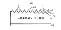
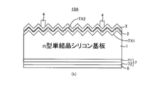
- FIG. 7 is a schematic diagram showing a configuration of another photoelectric conversion device according to the first embodiment.
- the photoelectric conversion device according to Embodiment 1 may be a photoelectric conversion device 10A illustrated in FIG.
- photoelectric conversion device 10 ⁇ / b> A is obtained by replacing passivation film 5 and electrode 6 of photoelectric conversion device 10 shown in FIG. 1 with amorphous thin film 7 and electrode 8, and the others are photoelectric conversion devices. 10 is the same.
- the amorphous thin film 7 is disposed in contact with the back surface of the n-type single crystal silicon substrate 1.
- the electrode 8 is disposed in contact with the amorphous thin film 7.
- the electrode 8 is made of, for example, Al.
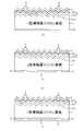
- FIG. 8 is a schematic diagram showing the configuration of the amorphous thin film 7 shown in FIG.
- amorphous thin film 7 includes an i-type amorphous thin film 71 and an n-type amorphous thin film 72 (see (a)).
- the i-type amorphous thin film 71 is made of the same material as the i-type amorphous thin film 21 described above.
- the i-type amorphous thin film 71 has a thickness of 10 to 20 nm.
- the n-type amorphous thin film 72 is disposed in contact with the i-type amorphous thin film 71.
- the n-type amorphous thin film 72 is one of n-type a-SiGe, n-type a-Ge, n-type a-SiC, n-type a-SiN, n-type a-SiO, and n-type a-SiCO. Generally, it consists of an n-type amorphous thin film containing a group IV element.
- the n-type amorphous thin film 72 has a thickness of 10 to 20 nm. Further, the n-type amorphous thin film 72 contains phosphorus (P) as an n-type dopant, and the P concentration is, for example, 1 ⁇ 10 18 cm ⁇ 3 to 1 ⁇ 10 19 cm ⁇ 3 .
- the combination of the material of the i-type amorphous thin film 71 and the material of the n-type amorphous thin film 72 is arbitrary, but the i-type amorphous thin film 71 is made of i-type a-Si, and the n-type amorphous thin film 71 A combination in which the thin film 72 is made of n-type a-Si is preferable.
- the amorphous thin film 7 may be composed of an n-type amorphous thin film 73 (see FIG. 8B).
- N-type amorphous thin film 73 is disposed in contact with the back surface of n-type single crystal silicon substrate 1.
- the n-type amorphous thin film 73 is made of the same material as that of the n-type amorphous thin film 72, and has a concentration of 1 ⁇ 10 18 cm ⁇ 3 to 1 ⁇ 10 19 cm ⁇ 3 as an n-type dopant. Including.
- the n-type amorphous thin film 73 has a thickness of 20 to 40 nm.
- the amorphous thin film 7 includes at least an n-type amorphous thin film (n-type amorphous thin film 72 or n-type amorphous thin film 73).
- the photoelectric conversion device 10A is provided with an amorphous thin film 2 in contact with the surface of the n-type single crystal silicon substrate 1 on which the concavo-convex structure TX1 is formed, and is in contact with the back surface of the n-type single crystal silicon substrate 1 to be amorphous. Since the thin film 7 is provided, the surface of the n-type single crystal silicon substrate 1 on which the concavo-convex structure TX1 is formed is passivated by the amorphous thin film 2, and the back surface of the n-type single crystal silicon substrate 1 is amorphous. Passivated by the thin film 7.
- the i-type amorphous thin film 71 has a greater passivation effect on the back surface of the n-type single crystal silicon substrate 1 than the n-type amorphous thin films 72 and 73.
- amorphous thin film 7 by forming the amorphous thin film 7 by the i-type amorphous thin film 71 and the n-type amorphous thin film 72, carriers (electrons and electrons) at the interface between the n-type single crystal silicon substrate 1 and the amorphous thin film 7 are formed. Hole recombination can be further reduced.
- the photoelectric conversion device 10A has a structure in which the amorphous thin films 2 and 7 are arranged on the light incident side and the back surface side of the n-type single crystal silicon substrate 1, respectively, when the photoelectric conversion device 10A is manufactured, the n-type Thermal strain applied to the single crystal silicon substrate 1 becomes uniform in the thickness direction, and warpage of the n-type single crystal silicon substrate 1 can be suppressed.
- the same effect as that in the photoelectric conversion device 10 can be obtained.
- 9 to 11 are first to third process diagrams showing a method for manufacturing the photoelectric conversion device 10A shown in FIG. 7, respectively.
- the amorphous thin film 2 is made of i-type amorphous silicon and p-type amorphous silicon
- the amorphous thin film 7 is made of i-type amorphous silicon and n.
- a method for manufacturing the photoelectric conversion device 10A will be described by taking as an example the case of a type amorphous silicon.
- process (a) shown in FIG. 4 when manufacturing of photoelectric conversion device 10A is started, the same process as process (a) shown in FIG. 4 is performed, and n-type single crystal silicon substrate 30 is cleaned (process (a)). ).
- Step (c) Thereafter, the same process as the process (d) shown in FIG. 4 is performed, and the i-type amorphous thin film 21 and the p-type amorphous thin film 24 are sequentially laminated along the concavo-convex structure TX1 of the n-type single crystal silicon substrate 1. (Step (c)).
- i-type amorphous silicon and n-type amorphous silicon are sequentially stacked on the back surface of the n-type single crystal silicon substrate 1 by plasma CVD.
- the i-type amorphous thin film 71 and the n-type amorphous thin film 72 are sequentially deposited on the back surface of the n-type single crystal silicon substrate 1 (step (d)).
- i-type amorphous silicon is formed using, for example, SiH 4 gas and H 2 gas
- n-type amorphous silicon is formed using, for example, SiH 4 gas, H 2 gas, and phosphine (PH 3 ) gas. It is formed using.
- step (d) the same step as step (e) shown in FIG. 5 is performed to etch the surface of p-type amorphous thin film 24 to form concavo-convex structure TX2 (step) (E)).
- step (f) the amorphous thin film 2 composed of the i-type amorphous thin film 21 and the p-type amorphous thin film 22 is formed (step (f)).
- the transparent conductive film 3 made of ITO is formed on the p-type amorphous thin film 22 in contact with the p-type amorphous thin film 22 by sputtering (step (g)).
- step (g) an Ag paste is applied by screen printing, and the applied Ag paste is baked to form electrode 4 on transparent conductive film 3. Further, Al is vapor-deposited on the n-type amorphous thin film 72 to form the electrode 8. Thus, the photoelectric conversion device 10A is completed (step (h)).
- the photoelectric conversion device 10A is manufactured by forming the amorphous thin films 2 and 7 on both surfaces of the n-type single crystal silicon substrate 1 by the plasma CVD method, respectively.
- the thermal strain applied to the n-type single crystal silicon substrate 1 from the thickness direction becomes uniform, and the warpage of the n-type single crystal silicon substrate 1 can be suppressed.
- the amorphous thin film 2 is composed of an i-type amorphous thin film 21 and a p-type amorphous thin film 22, and the amorphous thin film 7 is an i-type amorphous thin film 71.
- the method for manufacturing the photoelectric conversion device 10A has been described by taking the case of the n-type amorphous thin film 72 as an example.
- the amorphous thin film 2 is made of the p-type amorphous thin film 23 and the amorphous thin film 7 is n 9A, the photoelectric conversion device 10A performs the step (c) shown in FIG.
- step (d) shown in FIG. 9 is replaced with the step of depositing the n-type amorphous thin film 73 on the back surface of the n-type single crystal silicon substrate 1 by plasma CVD.
- step (e) the p-type amorphous thin film 23 is etched with an etching gas. It is prepared according to process diagram instead etching to process.
- the photoelectric conversion device 10A is It is manufactured according to the process chart shown in FIGS.
- the i-type amorphous thin film 71 is made of any of i-type a-SiGe, i-type a-Ge, i-type a-SiC, i-type a-SiN, i-type a-SiO, and i-type a-SiCO.
- the material gas is as described above.
- n-type amorphous thin films 72 and 73 are made of n-type a-SiGe, SiH 4 gas, GeH 4 gas, PH 3 gas and H 2 gas are used, and the n-type amorphous thin films 72 and 73 are When n-type a-Ge is used, GeH 4 gas, PH 3 gas and H 2 gas are used. When the n-type amorphous thin films 72 and 73 are made of n-type a-SiC, SiH 4 gas and CH 4 gas are used.
- n-type amorphous thin films 72 and 73 are made of n-type a-SiN, SiH 4 gas, NH 3 gas, PH 3 gas and H 2 gas are used, and when the n-type amorphous thin films 72 and 73 are made of n-type a-SiO, SiH 4 gas, O 2 gas, PH 3 gas, and H 2 gas are used, and the n-type amorphous thin films 72 and 73 are n-type. If it made of a-SiCO, SiH 4 gas, CH 4 gas , O 2 gas, PH 3 gas and H 2 gas is used.
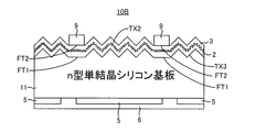
- FIG. 12 is a schematic diagram showing a configuration of still another photoelectric conversion device according to the first embodiment.
- the photoelectric conversion device according to Embodiment 1 may be a photoelectric conversion device 10B illustrated in FIG.
- photoelectric conversion device 10 ⁇ / b> B is obtained by replacing n-type single crystal silicon substrate 1 with n-type single crystal silicon substrate 11 and replacing electrode 4 with electrode 9 in photoelectric conversion device 10 shown in FIG. 1. Others are the same as the photoelectric conversion device 10.
- the n-type single crystal silicon substrate 11 has a (100) plane orientation, a specific resistance of 0.1 to 10 ⁇ cm, and a thickness of 100 ⁇ m to 300 ⁇ m.
- the n-type single crystal silicon substrate 11 has a concavo-convex structure TX3 provided on the surface on the light incident side and a flat surface FT1 provided on a portion facing the electrode 9 on the surface on the light incident side.
- the uneven structure TX3 has the same uneven size as the uneven structure TX1 shown in FIG.
- the electrode 9 is disposed in contact with the flat surface FT2 of the transparent conductive film 3 facing the flat surface FT1.
- the amorphous thin film 2 is disposed in contact with the concavo-convex structure TX3 and the flat surface FT1 of the n-type single crystal silicon substrate 11, and has the concavo-convex structure TX2 on the surface on the light incident side.
- the transparent conductive film 3 is disposed along the uneven structure TX3 and the flat surface FT1 of the n-type single crystal silicon substrate 11, and faces the flat surface FT1 among the surfaces on the light incident side.
- a part has a flat surface FT2.
- the amorphous thin film 2 is in contact with the n-type single crystal silicon substrate 11 on the flat surface FT1 below the electrode 9.
- the contact area between the amorphous thin film 2 and the n-type single crystal silicon substrate 11 decreases below the electrode 9. Therefore, recombination of carriers (electrons and holes) at the interface between the amorphous thin film 2 and the n-type single crystal silicon substrate 11 can be further reduced as compared with the case where the n-type single crystal silicon substrate 1 is used.
- the same effects as the photoelectric conversion device 10 can be obtained.
- the photoelectric conversion device 10B performs the step (c) shown in FIG. 4 in the process diagrams shown in FIGS. 4 to 6 with the n-type facing the electrode 9 on the light incident surface of the n-type single crystal silicon substrate 11.
- a portion of the single crystal silicon substrate 11 is covered with a resist, and the light incident side surface not covered with the resist is manufactured according to a process diagram in place of etching with alkali.
- the photoelectric conversion device according to Embodiment 1 may be the one in which the same change as the change from the photoelectric conversion device 10 to the photoelectric conversion device 10B is applied to the photoelectric conversion device 10A.
- the photoelectric conversion device performs step (b) shown in FIG. 9 in the process diagrams shown in FIGS. 9 to 11 to face the electrode 9 on the light incident side surface of the n-type single crystal silicon substrate 11.
- a part of n-type single crystal silicon substrate 11 is covered with a resist, and the light incident side surface not covered with the resist is manufactured according to a process diagram in place of etching with alkali.
- this photoelectric conversion device similarly to the photoelectric conversion device 10B, carriers (electrons and electrons) at the interface between the amorphous thin film 2 and the n-type single crystal silicon substrate 11 are used as compared with the case where the n-type single crystal silicon substrate 1 is used. Hole recombination can be further reduced.
- the photoelectric conversion device according to Embodiment 1 may be one in which n-type single crystal silicon substrates 1 and 11 are replaced with n-type polycrystalline silicon substrates.
- the surface on the light incident side of the n-type polycrystalline silicon substrate is roughened by dry etching.
- a photoelectric conversion apparatus provided with an n-type polycrystalline silicon substrate is manufactured according to the same manufacturing method as any manufacturing method of the photoelectric conversion apparatuses 10, 10A, and 10B mentioned above.
- the photoelectric conversion device according to Embodiment 1 is obtained by replacing the n-type single crystal silicon substrates 1 and 11 of the photoelectric conversion devices 10, 10A, and 10B with a p-type single crystal silicon substrate or a p-type polycrystalline silicon substrate. May be.
- the p-type single crystal silicon substrate has a (100) plane orientation, a specific resistance of 0.1 to 10 ⁇ cm, and a thickness of 100 ⁇ m to 300 ⁇ m.
- the p-type polycrystalline silicon substrate has a specific resistance of 0.1 to 10 ⁇ cm and a thickness of 100 ⁇ m to 300 ⁇ m, and the surface on the light incident side is roughened by dry etching.
- the amorphous thin film 2 is made of an i-type amorphous thin film and an n-type amorphous thin film, or an n-type amorphous thin film. Specific examples of the i-type amorphous thin film and the n-type amorphous thin film are as described above.
- the amorphous thin film 7 is composed of an i-type amorphous thin film and a p-type amorphous thin film, or a p-type amorphous thin film. Specific examples of the i-type amorphous thin film and the p-type amorphous thin film are as described above.
- a photoelectric conversion device including a p-type single crystal silicon substrate or a p-type polycrystalline silicon substrate is obtained by converting an n-type amorphous thin film into a p-type amorphous film in any of the manufacturing methods of the photoelectric conversion devices 10, 10A, and 10B described above. It is manufactured according to a manufacturing method in which a p-type amorphous thin film is replaced with an n-type amorphous thin film.
- the photoelectric conversion device is disposed in contact with the first concavo-convex structure, the crystalline silicon substrate provided with the first concavo-convex structure having the first concavo-convex size on the surface on the light incident side,
- a second concavo-convex structure having a second concavo-convex size smaller than the first concavo-convex size is provided with an amorphous thin film provided on the light incident side surface, and a pn junction is formed by the amorphous thin film and the crystalline silicon substrate. Or what is necessary is just to form a pin junction.
- FIG. 13 is a schematic diagram illustrating the configuration of the photoelectric conversion apparatus according to the second embodiment.
- photoelectric conversion device 100 according to Embodiment 2 replaces n-type single crystal silicon substrate 1 of photoelectric conversion device 10 shown in FIG. Is replaced with the amorphous thin film 102, the electrode 4 is replaced with the electrode 104, and the rest is the same as the photoelectric conversion device 10.
- the n-type single crystal silicon substrate 101 has a p-type diffusion region 101p on the light incident side.
- the p-type diffusion region 101p has a diffusion depth of 0.01 ⁇ m to 0.1 ⁇ m, for example, and is disposed in contact with the concavo-convex structure TX1.
- the p-type diffusion region 101p contains B as a p-type dopant, and the concentration of B is, for example, 10 17 cm ⁇ 3 to 10 18 cm ⁇ 3 .
- the n-type single crystal silicon substrate 101 includes the bulk region 101b having the n-type conductivity and the p-type diffusion region 101p having the p-type conductivity, and has a built-in pn junction on the light incident side. .
- n-type single crystal silicon substrate 101 The other description of the n-type single crystal silicon substrate 101 is the same as the description of the n-type single crystal silicon substrate 1.
- the amorphous thin film 102 is disposed on the p-type diffusion region 101p in contact with the p-type diffusion region 101p of the n-type single crystal silicon substrate 101.
- the amorphous thin film 102 has a concavo-convex structure TX2 on the light incident side surface.
- the electrode 104 is made of Ag, for example.
- the electrode 104 penetrates the transparent conductive film 3 and the amorphous thin film 102 and is disposed in contact with a part of the p-type diffusion region 101 p of the n-type single crystal silicon substrate 101.
- the transparent conductive film 3 is disposed on the amorphous thin film 102 in contact with the amorphous thin film 102.
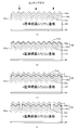
- FIG. 14 is a schematic diagram showing the configuration of the amorphous thin film 102 shown in FIG. Referring to FIG. 14, amorphous thin film 102 is composed of any one of amorphous thin films 102A to 102E.
- the amorphous thin film 102A includes an i-type amorphous thin film 102i and a p-type amorphous thin film 102p (see (a)).
- the i-type amorphous thin film 102i is disposed in contact with the concavo-convex structure TX1 of the n-type single crystal silicon substrate 101.
- the i-type amorphous thin film 102i has a thickness of 10 to 20 nm, for example.
- the p-type amorphous thin film 102p is disposed on the i-type amorphous thin film 102i in contact with the i-type amorphous thin film 102i, and has a concavo-convex structure TX2 on the surface on the light incident side.
- the p-type amorphous thin film 102p has a thickness of 1 to 200 nm.
- the p-type amorphous thin film 102p has an arbitrary B concentration.
- the i-type amorphous thin film 102i is made of the same material as the i-type amorphous thin film 21 described above.
- the p-type amorphous thin film 102p is made of the same material as the p-type amorphous thin film 22 described above.
- the material combination of the i-type amorphous thin film 102i and the p-type amorphous thin film 102p is arbitrary, but the i-type amorphous thin film 102i is made of i-type a-Si, and the p-type amorphous A combination in which the thin film 102p is made of p-type a-Si is preferable.
- the amorphous thin film 102B is made of an i-type amorphous thin film 103i (see FIG. 14B).
- the i-type amorphous thin film 103i is disposed in contact with the concavo-convex structure TX1 of the n-type single crystal silicon substrate 101, and has the concavo-convex structure TX2 on the light incident side surface.
- the i-type amorphous thin film 103i has a thickness of 1 to 200 nm, for example.
- the i-type amorphous thin film 103i is made of the same material as the i-type amorphous thin film 21 described above.
- the amorphous thin film 102C is composed of a p-type amorphous thin film 103p (see FIG. 14C).
- the p-type amorphous thin film 103p is disposed in contact with the concavo-convex structure TX1 of the n-type single crystal silicon substrate 101, and has the concavo-convex structure TX2 on the light incident side surface.
- the p-type amorphous thin film 103p has a thickness of 1 to 200 nm, for example.
- the p-type amorphous thin film 103p is made of the same material as the p-type amorphous thin film 22 described above.
- the amorphous thin film 102D includes an i-type amorphous thin film 102i and an n-type amorphous thin film 102n (see FIG. 14D).
- the n-type amorphous thin film 102n is disposed on the i-type amorphous thin film 102i in contact with the i-type amorphous thin film 102i, and has a concavo-convex structure TX2 on the light incident side surface.
- the n-type amorphous thin film 102n has a thickness of 1 to 200 nm and an arbitrary P concentration, for example.
- the n-type amorphous thin film 102n is made of the same material as the n-type amorphous thin film 72 described above.
- the material combination of the i-type amorphous thin film 102i and the n-type amorphous thin film 102n is arbitrary, but the i-type amorphous thin film 102i is made of i-type a-Si, and the n-type amorphous thin film 102i A combination in which the thin film 102n is made of n-type a-Si is preferable.
- the amorphous thin film 102E is composed of an n-type amorphous thin film 103n (see (e) of FIG. 14).
- the n-type amorphous thin film 103n is disposed in contact with the concavo-convex structure TX1 of the n-type single crystal silicon substrate 101, and has the concavo-convex structure TX2 on the light incident side surface.
- the n-type amorphous thin film 103n has a thickness of 1 to 200 nm, for example.
- the n-type amorphous thin film 103n is made of the same material as the n-type amorphous thin film 72 described above.
- the amorphous thin film 102 does not form a junction, the reflectance of the light is reduced on the light incident side, and the passivation effect on the surface of the n-type single crystal silicon substrate 101 on the light incident side. Therefore, it is made of the various materials described above.
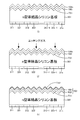
- 15 to 17 are first to third process diagrams showing a method for manufacturing the photoelectric conversion device 100 shown in FIG. 13, respectively.
- the amorphous thin film 102 is composed of an i-type amorphous thin film 102i (i-type a-Si) and a p-type amorphous thin film 102p (p-type a-Si).
- i-type a-Si i-type a-Si
- p-type amorphous thin film 102p p-type a-Si
- step (a) to step (c) when manufacturing of photoelectric conversion device 100 is started, the same steps as steps (a) to (c) shown in FIG. 4 are performed, and an n-type single crystal having passivation film 20 on the back surface.
- the silicon substrate 1 is manufactured (step (a) to step (c)).
- step (c) B is diffused from the surface side of the n-type single crystal silicon substrate 1 where the concavo-convex structure TX1 is formed, so that the p-type diffusion region 101p becomes the concavo-convex structure TX1 of the n-type single crystal silicon substrate 1.
- step (d) Form in contact (step (d)). Thereby, an n-type single crystal silicon substrate 101 is manufactured.
- the diffusion of B in the step (d) is performed, for example, by depositing a BSG (B-doped Silicate Glass) film on the n-type single crystal silicon substrate 1 by an APCVD (Atmospheric Chemical Vapor Deposition) method as a B source.
- the deposited BSG film is heat-treated at a temperature of about 800 ° C. in a nitrogen gas atmosphere, and then the BSG film is removed.
- the material gas is as described above.
- step (e) the same step as step (e) shown in FIG. 5 is performed to etch the light incident side surface of p-type amorphous thin film 104p (step (f)).
- step (f) the same step as step (e) shown in FIG. 5 is performed to etch the light incident side surface of p-type amorphous thin film 104p (step (f)).
- step (g) the same step as step (e) shown in FIG. 5 is performed to etch the light incident side surface of p-type amorphous thin film 104p (step (f)).
- step (g) the same step as step (e) shown in FIG. 5 is performed to etch the light incident side surface of p-type amorphous thin film 104p (step (f)).
- step (g) the same step as step (e) shown in FIG. 5 is performed to etch the light incident side surface of p-type amorphous thin film 104p (step (f)).
- step (g) the same step as step
- the transparent conductive film 3 is deposited on the amorphous thin film 102 by a sputtering method (step (h)).
- a part of the transparent conductive film 3 and the amorphous thin film 102 is etched at a desired interval using photolithography and etching to expose a part of the n-type single crystal silicon substrate 101 (step (i)).
- step (i) Ag paste is applied to the exposed portion of n-type single crystal silicon substrate 101, and the applied Ag paste is baked. As a result, the electrode 104 is formed (step (j)).
- steps (i) and (j) shown in FIG. 6 are sequentially performed to complete the photoelectric conversion device 100 (steps (k) and (l)).
- the photoelectric conversion device 100 is shown in FIG. It is manufactured according to the process diagram shown in FIG.
- the i-type amorphous thin films 102i and 103i are made of a material other than i-type a-Si, and the p-type amorphous thin films 102p and 103p are made of a material other than p-type a-Si. Even when 102n and 103n are made of a material other than n-type a-Si, the photoelectric conversion device 100 is manufactured according to the process diagrams shown in FIGS.
- the material gases for depositing the i-type amorphous thin films 102i and 103i, the p-type amorphous thin films 102p and 103p, and the n-type amorphous thin films 102n and 103n are as described above.
- the photoelectric conversion device 100 is disposed in contact with the light incident side surface of the n type single crystal silicon substrate 101, the n type single crystal silicon substrate 101 having the concavo-convex structure TX1 on the light incident side surface, and the light incident side surface. Is provided with the amorphous thin film 102 having the concavo-convex structure TX2, so that the reflectance of light on the surface on the light incident side can be lowered and the surface on the light incident side of the n-type single crystal silicon substrate 101 is passivated to form an n-type. Recombination of carriers (electrons and holes) at the interface between the single crystal silicon substrate 101 and the amorphous thin film 102 can be reduced.
- the photoexcited holes reach the electrode 104 through the p-type diffusion region 101p, so that the amorphous thin film 102 is more conductive than conducting the photoexcited holes to the electrode 104. This also contributes to a reduction in hole recombination and a reduction in light reflectance at the interface with the p-type diffusion region 101p.
- the amorphous thin film 102 is composed of any one of the amorphous thin films 102A, 102B, and 102D. This is because the i-type amorphous thin films 102i and 103i have a greater passivation effect on the surface of the n-type single crystal silicon substrate 101 than the p-type amorphous thin film 103p and the n-type amorphous thin film 103n containing the dopant. In view of the passivation effect, the simplification of the manufacturing process, and the reduction of the material cost, it is most preferable that the amorphous thin film 102 is constituted only by the i-type amorphous thin film 103i.
- the dopant concentration is relatively 10 16 cm ⁇ 3 to 10 17 cm ⁇ 3. It is preferable to set it low. By reducing the dopant concentration, the defect density at the interface between the amorphous thin film 102 and the p-type diffusion region 101p of the n-type single crystal silicon substrate 101 can be reduced, and at the interface between the amorphous thin film 102 and the p-type diffusion region 101p. This is because recombination can be reduced.
- the dopant concentration in the amorphous thin film 102 is gradually increased from the n-type single crystal silicon substrate 101 toward the transparent conductive film 3. May be.
- FIG. 18 is a schematic diagram showing a configuration of another photoelectric conversion apparatus according to the second embodiment.
- the photoelectric conversion device according to Embodiment 2 may be a photoelectric conversion device 100A illustrated in FIG.
- a photoelectric conversion device 100A is obtained by replacing n-type single crystal silicon substrate 101 with n-type single crystal silicon substrate 111 and replacing electrode 104 with electrode 114 in photoelectric conversion device 100 shown in FIG. 13. Others are the same as those of the photoelectric conversion device 100.
- the n-type single crystal silicon substrate 111 has a (100) plane orientation, a specific resistance of 0.1 to 10 ⁇ cm, and a thickness of 100 ⁇ m to 300 ⁇ m.
- the n-type single crystal silicon substrate 111 has a concavo-convex structure TX3 provided on the surface on the light incident side and a flat surface FT3 provided on a portion in contact with the electrode 114 on the surface on the light incident side.
- the uneven structure TX3 has the same uneven size as the uneven structure TX1 shown in FIG.
- the n-type single crystal silicon substrate 111 has a p-type diffusion region 111p on the light incident surface side.
- the p-type diffusion region 111p is disposed in contact with the concavo-convex structure TX3 on the light incident side of the n-type single crystal silicon substrate 111.
- the p-type diffusion region 111p has the same diffusion depth and B concentration as the p-type diffusion region 101p (see FIG. 13) of the photoelectric conversion device 100.
- the n-type single crystal silicon substrate 111 includes a bulk region 111b having an n-type conductivity type and a p-type diffusion region 111p having a p-type conductivity type, and incorporates a pn junction on the light incident side.
- the electrode 114 is made of Ag, for example. Electrode 114 penetrates transparent conductive film 3 and amorphous thin film 102, and is disposed in contact with flat surface FT3 of p-type diffusion region 111p of n-type single crystal silicon substrate 111.
- the electrode 114 is in contact with the flat surface FT3 of the n-type single crystal silicon substrate 111, so that the contact area between the n-type single crystal silicon substrate 111 and the electrode 114 is smaller than that of the photoelectric conversion device 100. Therefore, recombination of minority carriers (holes) at the interface between the n-type single crystal silicon substrate 111 and the electrode 114 can be further reduced as compared with the photoelectric conversion device 100. In the photoelectric conversion device 100A, the same effects as the photoelectric conversion device 100 can be obtained.
- the photoelectric conversion device 100A performs the step (c) shown in FIG. 15 in the process diagrams shown in FIGS. 15 to 17 in the n-type single crystal silicon substrate 111 on the light incident side surface n in contact with the electrode 114.
- a portion of the single crystal silicon substrate 111 is covered with a resist, and the light incident side surface not covered with the resist is manufactured according to a process diagram in place of etching with alkali.
- the photoelectric conversion devices 100 and 100A using the n-type single crystal silicon substrates 101 and 111 have been described.
- the photoelectric conversion device according to the second embodiment is not limited to this.
- the type single crystal silicon substrates 101 and 111 may be replaced with n-type polycrystalline silicon substrates.
- the surface on the light incident side of the n-type polycrystalline silicon substrate is roughened by dry etching.
- a photoelectric conversion apparatus provided with an n-type polycrystalline silicon substrate is manufactured according to the same manufacturing method as the manufacturing method of any of the photoelectric conversion apparatuses 100 and 100A described above.
- the photoelectric conversion device according to the second embodiment may be one in which the n-type single crystal silicon substrates 101 and 111 of the photoelectric conversion devices 100 and 100A are replaced with a p-type single crystal silicon substrate or a p-type polycrystalline silicon substrate. Good.
- the p-type single crystal silicon substrate has a (100) plane orientation, a specific resistance of 0.1 to 10 ⁇ cm, and a thickness of 100 ⁇ m to 300 ⁇ m.
- the p-type polycrystalline silicon substrate has a specific resistance of 0.1 to 10 ⁇ cm and a thickness of 100 ⁇ m to 300 ⁇ m, and the surface on the light incident side is roughened by dry etching.
- a photoelectric conversion device including a p-type single crystal silicon substrate or a p-type polycrystalline silicon substrate is obtained by replacing the p-type diffusion region with an n-type diffusion region in any one of the manufacturing methods of the photoelectric conversion devices 100 and 100A described above. Manufactured according to.
- the photoelectric conversion device includes various photoelectric conversion devices. Therefore, in the photoelectric conversion device according to the second embodiment, the first concavo-convex structure having the first concavo-convex size is provided on the surface on the light incident side, is provided in contact with the surface on the light incident side, and is a bulk region.
- a crystalline silicon substrate including a diffusion region having a conductivity type opposite to that of the first conductive layer, a bulk region, and a first concavo-convex structure, and a second concavo-convex size smaller than the first concavo-convex size. What is necessary is just to provide the 2nd uneven structure with the amorphous thin film provided in the surface by the side of light incidence.
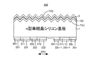
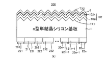
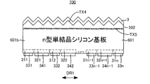
- FIG. 19 is a schematic diagram illustrating a configuration of a photoelectric conversion apparatus according to the third embodiment.
- photoelectric conversion device 200 according to Embodiment 3 deletes electrode 4 of photoelectric conversion device 10 shown in FIG. 1, replaces amorphous thin film 2 with amorphous thin film 102, and forms passivation film 5.
- the electrode 6 is replaced with amorphous thin films 201 to 20n (n is an integer of 2 or more), 211 to 21n-1, electrodes 221 to 22n, 231 to 23n-1, and the others are the photoelectric conversion device 10 Is the same.
- the amorphous thin film 102 is disposed in contact with the concavo-convex structure TX1 of the n-type single crystal silicon substrate 1, and has a concavo-convex structure TX2 on the surface on the light incident side.
- the amorphous thin film 102 is composed of any one of the amorphous thin films 102A to 102E (see FIGS. 14A to 14E).
- the amorphous thin film 102 has a thickness of 1 to 200 nm, for example.
- the amorphous thin films 201 to 20n are in contact with the back surface of the n-type single crystal silicon substrate 1, and are alternately arranged with the amorphous thin films 211 to 21n-1 in the in-plane direction DR1 of the n-type single crystal silicon substrate 1. .
- the amorphous thin films 211 to 21n-1 are in contact with the back surface of the n-type single crystal silicon substrate 1, and are alternately arranged with the amorphous thin films 201 to 20n in the in-plane direction DR1.
- the electrodes 221 to 22n are disposed in contact with the amorphous thin films 201 to 20n, respectively.
- the electrodes 231 to 23n-1 are disposed in contact with the amorphous thin films 211 to 21n-1, respectively.
- Each of the electrodes 221 to 22n and 231 to 23n-1 is made of, for example, Al.
- FIG. 20 is a schematic diagram showing the configuration of the amorphous thin film 201 shown in FIG. Referring to FIG. 20, the amorphous thin film 201 is composed of an amorphous thin film 201A or an amorphous thin film 201B.
- the amorphous thin film 201A includes an i-type amorphous thin film 201i and an n-type amorphous thin film 201n (see FIG. 20A).
- the i-type amorphous thin film 201 i is disposed in contact with the back surface of the n-type single crystal silicon substrate 1.
- the i-type amorphous thin film 201i has a thickness of 10 to 20 nm, for example.
- the i-type amorphous thin film 201i is made of the same material as the i-type amorphous thin film 21 described above.
- the n-type amorphous thin film 201n is disposed in contact with the i-type amorphous thin film 201i.
- the n-type amorphous thin film 201n has a thickness of 10 to 20 nm, for example.
- the n-type amorphous thin film 201n has a P concentration of, for example, 1 ⁇ 10 18 cm ⁇ 3 to 1 ⁇ 10 19 cm ⁇ 3 .
- the n-type amorphous thin film 201n is made of the same material as the n-type amorphous thin film 72 described above.
- the combination of the material of the i-type amorphous thin film 201i and the material of the n-type amorphous thin film 201n is arbitrary, but the i-type amorphous thin film 201i is made of i-type a-Si, and the n-type amorphous thin film 201i A combination in which the thin film 201n is made of n-type a-Si is preferable.
- the amorphous thin film 201B is composed of an n-type amorphous thin film 201n ′ (see FIG. 20B).
- N-type amorphous thin film 201 n ′ is disposed in contact with the back surface of n-type single crystal silicon substrate 1.
- the n-type amorphous thin film 201n ′ has a thickness of 20 to 40 nm, for example.
- the n-type amorphous thin film 201n ′ has a P concentration of 1 ⁇ 10 18 cm ⁇ 3 to 1 ⁇ 10 19 cm ⁇ 3 , for example.
- the n-type amorphous thin film 201n ′ is made of the same material as the n-type amorphous thin film 72 described above.
- the amorphous thin film 201 includes at least an n-type amorphous thin film.
- each of the amorphous thin films 202 to 20n shown in FIG. 19 is composed of either of the amorphous thin films 201A and 201B shown in FIG.
- FIG. 21 is a schematic diagram showing a configuration of another amorphous thin film 211 shown in FIG. Referring to FIG. 21, amorphous thin film 211 includes amorphous thin film 211A or amorphous thin film 211B.
- the amorphous thin film 211A includes an i-type amorphous thin film 211i and a p-type amorphous thin film 211p (see FIG. 21A).
- the i-type amorphous thin film 211 i is disposed in contact with the back surface of the n-type single crystal silicon substrate 1.
- the i-type amorphous thin film 211i has a thickness of 10 to 20 nm, for example.
- the i-type amorphous thin film 211i is made of the same material as the i-type amorphous thin film 21 described above.
- the p-type amorphous thin film 211p is disposed in contact with the i-type amorphous thin film 211i.
- the p-type amorphous thin film 211p has a thickness of 10 to 20 nm, for example.
- the p-type amorphous thin film 211p has a B concentration of, for example, 1 ⁇ 10 18 cm ⁇ 3 to 1 ⁇ 10 19 cm ⁇ 3 .
- the p-type amorphous thin film 211p is made of the same material as the p-type amorphous thin film 22 described above.
- the combination of the material of the i-type amorphous thin film 211i and the material of the p-type amorphous thin film 211p is arbitrary, but the i-type amorphous thin film 211i is made of i-type a-Si, and the p-type amorphous A combination in which the thin film 211p is made of p-type a-Si is preferable.
- the amorphous thin film 211B is made of a p-type amorphous thin film 211p ′ (see FIG. 21B).
- the p-type amorphous thin film 211p ′ is disposed in contact with the back surface of the n-type single crystal silicon substrate 1.
- the p-type amorphous thin film 211p ′ has a thickness of 20 to 40 nm, for example.
- the p-type amorphous thin film 211p ′ has a B concentration of, for example, 1 ⁇ 10 18 cm ⁇ 3 to 1 ⁇ 10 19 cm ⁇ 3 .
- the p-type amorphous thin film 211p ′ is made of the same material as the p-type amorphous thin film 22 described above.
- the amorphous thin film 211 includes at least a p-type amorphous thin film.
- each of the amorphous thin films 212 to 21n-1 shown in FIG. 19 is composed of either of the amorphous thin films 211A and 211B shown in FIG.
- the area occupancy ratio which is the ratio of the total area of the amorphous thin films 211 to 21n-1 to the area of the n-type single crystal silicon substrate 1 is 60 to 93%.
- the area occupation ratio which is the ratio of the total area of the thin films 201 to 20n to the area of the n-type single crystal silicon substrate 1, is 5 to 20%.
- the reason why the area occupancy of the amorphous thin films 211 to 21n-1 is larger than the area occupancy of the amorphous thin films 201 to 20n is that the photo-excited electrons in the n-type single crystal silicon substrate 1 and Holes are easily separated by a pn junction (amorphous thin film 211 to 21n-1 / n-type single crystal silicon substrate 1 including at least a p-type amorphous thin film), and power generation of photoexcited electrons and holes is facilitated. This is to increase the contribution rate.
- incident light enters the n-type single crystal silicon substrate 1 from the transparent conductive film 3 side.
- there is no electrode on the light incident side and there are two concavo-convex structures TX1 and TX2 having different concavo-convex sizes, so that the reflectance of light is reduced, and more incident light is n-type single crystal silicon. Incident on the substrate 1.
- the photoexcited electrons reach the amorphous thin films 201 to 20n by diffusion, and reach the electrodes 221 to 22n through the amorphous thin films 201 to 20n.
- the photoexcited electrons in the vicinity of the concavo-convex structure TX1 of the n-type single crystal silicon substrate 1 cause the amorphous thin film 102 and the n-type single crystal silicon substrate 1 to pass through the surface of the n-type single crystal silicon substrate 1 by the passivation effect. It becomes difficult to recombine at the interface with the type single crystal silicon substrate 1, and it becomes easy to diffuse into the amorphous thin films 201 to 20n.
- photoexcited holes reach the amorphous thin films 211 to 21n-1 by diffusion, and reach the electrodes 231 to 23n-1 through the amorphous thin films 211 to 21n-1.
- holes photoexcited in the vicinity of the concavo-convex structure TX1 of the n-type single crystal silicon substrate 1 are separated from the amorphous thin film 102 by the passivation effect of the surface of the n-type single crystal silicon substrate 1 by the amorphous thin film 102. It becomes difficult to recombine at the interface with the n-type single crystal silicon substrate 1, and it becomes easy to diffuse into the amorphous thin films 211 to 21n-1.
- the photoelectric conversion device 200 is a back contact type photoelectric conversion device that extracts photoexcited carriers (electrons and holes) from the back surface.
- the photoelectric conversion device 200 is arranged in contact with the n-type single crystal silicon substrate 1 on which the concavo-convex structure TX1 is formed, and the concavo-convex structure TX1, and has a non-convex structure TX2 formed on the surface on the light incident side. Since the crystalline thin film 102 is provided, the reflectivity for incident light can be reduced on the light incident side surface, and carriers at the interface between the amorphous thin film 102 and the concavo-convex structure TX1 of the n-type single crystal silicon substrate 1 can be reduced. Recombination of (electrons and holes) can be reduced.
- 22 to 25 are first to fourth process diagrams showing a method for manufacturing the photoelectric conversion device 200 shown in FIG. 19, respectively.
- the amorphous thin film 102 includes an i-type amorphous thin film 102i and an n-type amorphous thin film 102n (see FIG. 14D), and the amorphous thin films 201 to 20n.
- a method for manufacturing the photoelectric conversion device 200 will be described by taking the case of the p-type amorphous thin film 211p (see FIG. 21A) as an example.
- n-type single crystal silicon substrate 30 is cleaned (step (a)).
- n-type single crystal silicon substrate 30 is anisotropically etched with alkali to form the concavo-convex structure TX1 (step (b)). Thereby, n-type single crystal silicon substrate 1 is formed.
- a resist is applied to the entire surface of p-type amorphous thin film 240p, and the applied resist is patterned by photolithography to form a resist pattern 250 (step (step (2)). e)).
- the p-type amorphous thin film 240p is etched using the resist pattern 250 as a mask to form n ⁇ 1 p-type amorphous thin films 201p (step (f)).
- step (g) resist pattern 250 is removed. Then, the n-type amorphous thin film 260 is removed by lift-off. As a result, amorphous thin films 201 to 20n and amorphous thin films 211 to 21n-1 are formed on the back surface of n-type single crystal silicon substrate 1.
- the transparent conductive film 3 is formed on the amorphous thin film 102 by a sputtering method (step (j)).
- step (j) Al paste is applied onto amorphous thin films 201 to 20n and amorphous thin films 211 to 21n-1, and the applied Al paste is baked to form electrode 221. To 22n and 231 to 23n-1. Thereby, the photoelectric conversion device 200 is completed (step (k)).
- the photoelectric conversion device 200 is shown in FIG. It is manufactured according to the process diagram shown in FIG.
- the amorphous thin film 102 is made of the i-type amorphous thin film 103i shown in FIG. 14B, only the i-type amorphous thin film is deposited in step (c) shown in FIG.
- the surface of the light incident side of the i-type amorphous thin film thus etched is etched in the step (h) shown in FIG.
- the amorphous thin film 102 is composed of the p-type amorphous thin film 103p shown in FIG. 14C, only the p-type amorphous thin film is deposited in the step (c) shown in FIG. In the step (h) shown in FIG. 24, the surface on the light incident side of the p-type amorphous thin film thus etched is etched.
- the amorphous thin film 102 is composed of the i-type amorphous thin film 102i / p-type amorphous thin film 102p shown in FIG. 14A
- the step (c) shown in FIG. The thin film 102i and the p-type amorphous thin film are sequentially deposited, and the surface on the light incident side of the deposited p-type amorphous thin film is etched in step (h) shown in FIG.
- the amorphous thin film 102 is composed of the n-type amorphous thin film 103n shown in FIG. 14E, only the n-type amorphous thin film is deposited in the step (c) shown in FIG. The surface of the light incident side of the n-type amorphous thin film thus etched is etched in the step (h) shown in FIG.
- the photoelectric conversion device 200 is shown in FIGS. Manufactured according to the process diagram shown. In this case, the deposition of the i-type amorphous thin film is omitted in step (d) of FIG.
- the amorphous thin films 201 to 20n are i-type amorphous thin films 201i / n-type amorphous thin films 201n, and the amorphous thin films 211 to 21n-1 are p-type amorphous thin films.
- the thin film 211p ′ may consist of only the amorphous thin film 201-20n, which consists of only the n-type amorphous thin film 201n ′, and the amorphous thin film 211-21n-1 includes the i-type amorphous thin film 211i / p. It may consist of a type amorphous thin film 211p.
- the photoelectric conversion device 200 is manufactured according to the process diagrams shown in FIGS.
- both the i-type amorphous thin film 102i and the p-type amorphous thin film 104p are etched using the resist pattern 250 as a mask.
- the amorphous thin films 201 to 20n are made of the i-type amorphous thin film 201i / n-type amorphous thin film 201n, and the amorphous thin films 211 to 21n-1 are made of only the p-type amorphous thin film 211p ′.
- the i-type amorphous thin film 102 i and the n-type amorphous thin film 104 n are sequentially stacked.
- the i-type amorphous film is formed using the resist pattern 250 as a mask. Both the thin film 102i and the n-type amorphous thin film 104n are etched, and a p-type amorphous thin film is deposited in step (g) of FIG.
- the photoelectric conversion device 200 is shown in FIGS. Manufactured according to the process diagram.
- the photoelectric conversion device 200 includes an amorphous thin film 102 on the light incident side of the n-type single crystal silicon substrate 1, and amorphous thin films 201 to 20n and an amorphous thin film 211 on the back side of the n-type single crystal silicon substrate 1. ⁇ 21n ⁇ 1, the strain applied to the n-type single crystal silicon substrate 1 in the manufacturing process is uniform in the thickness direction. Accordingly, warpage of the n-type single crystal silicon substrate 1 can be suppressed.
- the photoelectric conversion device 200 is described as including the n-type single crystal silicon substrate 1, in Embodiment 3, the photoelectric conversion device 200 is not limited to this and includes the p-type single crystal silicon substrate. Also good.
- the amorphous thin films 201 to 20n are i-type amorphous thin film / p-type amorphous thin film or p-type amorphous thin film
- the amorphous thin films 211 to 21n-1 are i-type non-crystalline thin films. It consists of a crystalline thin film / n-type amorphous thin film or an n-type amorphous thin film.
- the photoelectric conversion apparatus 200 is manufactured according to the process diagrams shown in FIGS. 22 to 25 even when the p-type single crystal silicon substrate is provided.
- the amorphous thin film 102 is disposed in contact with the concavo-convex structure TX1 formed on the light incident side surface of the n-type single crystal silicon substrate or the p-type single crystal silicon substrate, and the light of the amorphous thin film 102 is Photoelectric conversion in which a concavo-convex structure TX2 is arranged on the surface on the incident side, and amorphous thin films 201 to 20n and 211 to 21n-1 for back contact are formed on the back surface of an n-type single crystal silicon substrate or a p-type single crystal silicon substrate The apparatus has been described.
- the photoelectric conversion device is arranged in contact with the concavo-convex structure TX1 and the single crystal silicon substrate having the concavo-convex structure TX1 on the surface on the light incident side, and has a non-convex structure TX2 on the surface on the light incident side.
- a crystalline thin film 102 and amorphous thin films 201 to 20n and 211 to 21n-1 for forming a back contact may be provided.
- FIG. 26 is a schematic diagram illustrating a configuration of a photoelectric conversion apparatus according to the fourth embodiment.
- photoelectric conversion device 300 according to Embodiment 4 deletes amorphous thin films 201 to 20n and 211 to 21n-1 of photoelectric conversion device 200 shown in FIG. 1 is replaced with the n-type single crystal silicon substrate 301, and the electrodes 221 to 22n and 231 to 23n-1 are replaced with the electrodes 331 to 33n and 341 to 34n-1, and the others are the same as the photoelectric conversion device 200. is there.
- the n-type single crystal silicon substrate 301 has a concavo-convex structure TX1 on the light incident side surface, and n-type diffusion regions 311 to 31n and p-type diffusion regions 321 to 32n-1 on the back surface side.
- the n-type single crystal silicon substrate 301 includes a bulk region 301b, n-type diffusion regions 311 to 31n and p-type diffusion regions 321 to 32n-1, and a pn junction (p-type diffusion regions 321 to 32n-1).
- N-type single crystal silicon substrate 301) is built in the back side.
- n-type single crystal silicon substrate 301 is the same as that of the n-type single crystal silicon substrate 1.
- n-type diffusion regions 311 to 31n and the p-type diffusion regions 321 to 32n-1 are alternately arranged in the in-plane direction DR1 of the n-type single crystal silicon substrate 301 in contact with the back surface of the n-type single crystal silicon substrate 301. .
- the n-type diffusion regions 311 to 31n have, for example, a P concentration of 1 ⁇ 10 17 cm ⁇ 3 to 1 ⁇ 10 18 cm ⁇ 3
- the p-type diffusion regions 321 to 32n ⁇ 1 have, for example, 1 ⁇ 10 17 B concentration of cm ⁇ 3 to 1 ⁇ 10 18 cm ⁇ 3 .
- the n-type diffusion regions 311 to 31n and the p-type diffusion regions 321 to 32n-1 have a diffusion depth of 0.01 ⁇ m to 0.1 ⁇ m.
- the n-type diffusion regions 311 to 31n have the same length as the p-type diffusion regions 321 to 32n-1. Have.
- the area occupancy ratio which is the ratio of the total area of the p-type diffusion regions 321 to 32n-1 to the area of the n-type single crystal silicon substrate 301, is 60 to 93%, and the n-type diffusion regions 311 to 31n
- the area occupation ratio which is the ratio of the entire area to the area of the n-type single crystal silicon substrate 301, is 5 to 20%.
- the reason why the area occupancy of the p-type diffusion regions 321 to 32n-1 is larger than the area occupancy of the n-type diffusion regions 311 to 31n is that the electrons excited in the n-type single crystal silicon substrate 301 and This is because holes are easily separated by the pn junction (p-type diffusion regions 321 to 32n-1 / n-type single crystal silicon substrate 301), and the contribution ratio of photoexcited electrons and holes to power generation is increased.
- the electrodes 331 to 33n are disposed in contact with the n-type diffusion regions 311 to 31n, respectively.
- the electrodes 341 to 34n-1 are disposed in contact with the p-type diffusion regions 341 to 34n-1, respectively.
- the electrodes 331 to 33n and 341 to 34n-1 are made of, for example, Al.
- the power generation principle of the photoelectric conversion device 300 is the same as the power generation principle of the photoelectric conversion device 200 described above. Therefore, the photoelectric conversion device 300 is also a back-contact type photoelectric conversion device that extracts photoexcited carriers (electrons and holes) from the back surface.
- the photoelectric conversion device 300 includes an n-type single crystal silicon substrate 301 on which a concavo-convex structure TX1 is formed, an amorphous thin film 102 that is disposed in contact with the concavo-convex structure TX1, and has a concavo-convex structure TX2 formed on the light incident side surface. Therefore, it is possible to reduce the reflectance with respect to incident light on the surface on the light incident side, and at the same time carriers (electrons and holes) at the interface between the amorphous thin film 102 and the concavo-convex structure TX1 of the n-type single crystal silicon substrate 301. ) Recombination can be reduced.
- 27 to 30 are first to fourth process diagrams showing a method for manufacturing the photoelectric conversion device 300 shown in FIG. 26, respectively.
- a method for manufacturing the photoelectric conversion device 300 will be described by taking as an example the case where the amorphous thin film 102 includes an i-type amorphous thin film 102 i and an n-type amorphous thin film 102 n.
- n-type single crystal silicon substrate 30 is cleaned (step (a)).
- a BSG film 350B and an NSG (Non-doped Silicate Glass) film 350N are sequentially stacked on the back surface of the n-type single crystal silicon substrate 30 by the APCVD method (step (b)).
- a resist is applied to the entire surface of the NSG film 350N, and the applied resist is patterned by photolithography and etching to form a resist pattern 360 (step (c)).
- step (d) the NSG film 350N and the BSG film 350B are etched using the resist pattern 360 as a mask, and then the resist pattern 360 is removed.
- BSG films 350B-1 to 350Bn-1 and NSG films 350N-1 to 350Nn-1 are formed (step (d)).
- a PSG (Phosphorus Silicate Glass) film 350P is formed by APCVD so as to cover the back surface of n-type single crystal silicon substrate 30 and NSG films 350N-1 to 350Nn-1. (Step (e)).
- the n-type single crystal silicon substrate 30, the BSG films 350B-1 to 350Bn-1, the NSG films 350N-1 to 350Nn-1 and the PSG film 350P are heat-treated at a temperature of 800 ° C. in a nitrogen gas atmosphere. (Step (f)).
- B diffuses from the BSG films 350B-1 to 350B-n-1 into the n-type single crystal silicon substrate 30, and P of the PSG film 350P comes into the n-type from the portion in contact with the n-type single crystal silicon substrate 30. It diffuses into the single crystal silicon substrate 30.
- the NSG film 350N-1 is interposed between the BSG films 350B-1 to 350B-n-1 and the PSG film 350P. Since ⁇ 350Nn-1 exists, P does not diffuse into the n-type single crystal silicon substrate 30 from the PSG film 350P.
- the BSG films 350B-1 to 350B-n-1, the NSG films 350N-1 to 350N-n-1 and the PSG film 350P are removed.
- n-type diffusion regions 311 to 31n and p-type diffusion regions 321 to 32n-1 are formed on the back surface side of the n-type single crystal silicon substrate 30 (step (g)).
- the surface on the light incident side of the n-type single crystal silicon substrate 30 is anisotropically etched with alkali to form the concavo-convex structure TX1 (step (h). Thereby, the n-type single crystal silicon substrate 301 is manufactured. .
- process (j) the same process as the process (e) of FIG. 5 is performed to etch the light incident side surface of the n-type amorphous thin film 104n (process (j)).
- process (j) an n-type amorphous thin film 102n having a concavo-convex structure TX2 is formed on the light incident side surface, and the amorphous thin film 102 is disposed in contact with the concavo-convex structure TX1 of the n-type single crystal silicon substrate 301 (step). (K)).
- transparent conductive film 3 is deposited on amorphous thin film 102 by a sputtering method (step (l)).
- step (m) an Al paste is applied on the n-type diffusion regions 311 to 31n and the p-type diffusion regions 321 to 32n-1, and the applied Al paste is baked. As a result, electrodes 331 to 33n and 341 to 34n-1 are formed, and the photoelectric conversion device 300 is completed (step (m)).
- the photoelectric conversion device 300 is shown in FIG. Manufactured according to the process diagram shown in FIG.
- the amorphous thin film 102 is made of the i-type amorphous thin film 103i shown in FIG. 14B, only the i-type amorphous thin film is deposited in step (i) shown in FIG.
- the surface of the light incident side of the i-type amorphous thin film thus etched is etched in the step (j) shown in FIG.
- the amorphous thin film 102 is composed of the p-type amorphous thin film 103p shown in FIG. 14C, only the p-type amorphous thin film is deposited in step (i) shown in FIG. The surface on the light incident side of the p-type amorphous thin film thus etched is etched in the step (j) shown in FIG.
- the amorphous thin film 102 is composed of the i-type amorphous thin film 102i / p-type amorphous thin film 102p shown in FIG. 14A
- the step (i) shown in FIG. The thin film 102i and the p-type amorphous thin film are sequentially deposited, and the surface on the light incident side of the deposited p-type amorphous thin film is etched in the step (j) shown in FIG.
- amorphous thin film 102 is composed of the n-type amorphous thin film 103n shown in FIG. 14E, only the n-type amorphous thin film is deposited in the step (i) shown in FIG. The surface of the light incident side of the n-type amorphous thin film thus etched is etched in step (j) shown in FIG.
- the photoelectric conversion device 300 includes the n-type single crystal silicon substrate 301, the photoelectric conversion device 300 includes a p-type single crystal silicon substrate in Embodiment 4 without being limited thereto. Also good.
- the photoelectric conversion apparatus 300 is manufactured according to the process diagrams shown in FIGS. 27 to 30 even when the p-type single crystal silicon substrate is provided.
- the amorphous thin film 102 is disposed in contact with the concavo-convex structure TX1 formed on the light incident side surface of the n-type single crystal silicon substrate or the p-type single crystal silicon substrate, and the light of the amorphous thin film 102 is
- An uneven structure TX2 is disposed on the surface on the incident side, and n-type diffusion regions 311 to 31n and p-type diffusion regions 321 to 32n-1 for back contact are provided on the back side of the n-type single crystal silicon substrate or the p-type single crystal silicon substrate.
- the photoelectric conversion device is arranged in contact with the concavo-convex structure TX1 and the single crystal silicon substrate having the concavo-convex structure TX1 on the surface on the light incident side, and has the non-convex structure TX2 on the surface on the light incident side. What is necessary is just to provide the crystalline thin film 102 and the diffusion area
- FIG. 31 is a schematic diagram illustrating a configuration of a photoelectric conversion apparatus according to the fifth embodiment.
- photoelectric conversion device 400 according to Embodiment 5 replaces n-type single crystal silicon substrate 1 of photoelectric conversion device 10 shown in FIG. Is the same as the photoelectric conversion device 10 except that the amorphous thin film 402 is used.
- the n-type single crystal silicon substrate 401 has a concavo-convex structure TX5 on the light incident side surface.
- the height H3 and the width W3 are defined in the same manner as the height H2 and the width W2 shown in FIG.
- the height H3 is, for example, 1 nm to 40 nm, and the width W3 is 1 nm to 40 nm.
- the other description of the n-type single crystal silicon substrate 401 is the same as that of the n-type single crystal silicon substrate 1.
- the amorphous thin film 402 is disposed in contact with the concavo-convex structure TX5 of the n-type single crystal silicon substrate 401, and has a concavo-convex structure TX4 on the surface on the light incident side.
- the height H4 and the width W4 are defined in the same manner as the height H1 and the width W1 shown in FIG.
- the height H4 is, for example, 50 nm to 1 ⁇ m
- the width W4 is 50 nm to 1 ⁇ m.
- the concavo-convex structure TX4 has a larger concavo-convex size than the concavo-convex structure TX5.
- the amorphous thin film 402 has a configuration shown in FIG.
- the amorphous thin film 402 has the structure shown in FIG. 3A (i-type amorphous thin film 21 / p-type amorphous thin film 22)
- the i-type amorphous thin film 21 is formed of n-type single crystal silicon.
- the p-type amorphous thin film 22 is disposed in contact with the concavo-convex structure TX5 of the substrate 401, and is disposed in contact with the i-type amorphous thin film 21, and has a concavo-convex structure TX4 on the surface on the light incident side.
- the p-type amorphous thin film 23 has a concavo-convex structure TX5 of the n-type single crystal silicon substrate 401. And has a concavo-convex structure TX4 on the surface on the light incident side.
- the transparent conductive film 3 is disposed along the concavo-convex structure TX4 of the amorphous thin film 402, and has the concavo-convex structure TX4 on the surface on the light incident side.
- the passivation film 5 is disposed in contact with the back surface of the n-type single crystal silicon substrate 401, and the electrode 6 is disposed in contact with the back surface of the passivation film 5 and the n-type single crystal silicon substrate 401.
- the two concavo-convex structures TX4 and TX5 are arranged so as to change from a large concavo-convex size to a small concavo-convex size in the light incident direction.
- the two concavo-convex structures TX4 and TX5 are arranged so as to change from a large concavo-convex size to a small concavo-convex size with respect to the light incident direction, the light reflectance on the light incident side of the photoelectric conversion device 400 is increased. Can be reduced.
- i-type a-Si or the like is disposed in contact with the concavo-convex structure TX5 of the n-type single crystal silicon substrate 401. . Since i-type a-Si and the like are formed by the plasma CVD method, they are uniformly formed on the concavo-convex structure TX5 so as to cover the concavo-convex structure TX5 having the concavo-convex size described above. As a result, the surface of the n-type single crystal silicon substrate 401 on which the concavo-convex structure TX5 is formed is passivated by the amorphous thin film 402.
- the photoelectric conversion device 400 is manufactured according to the process chart shown in FIGS.
- the n-type single crystal silicon substrate 401 has the concavo-convex structure TX5 formed on the surface on the light incident side in the step (c) of FIG.
- the concavo-convex structure TX5 having a small concavo-convex size is formed by shortening the time of anisotropic etching with alkali.
- the concavo-convex structure TX5 may be formed using dry etching.
- the concavo-convex structure TX4 is formed on the surface of the amorphous thin film 402 on the light incident side.
- the concavo-convex structure TX4 having a large concavo-convex size is formed by lengthening the etching time with the gas containing fluorine atoms.
- photoelectric conversion device 400 is the same as the description of the photoelectric conversion device 10 in the first embodiment.
- FIG. 32 is a schematic diagram showing a configuration of another photoelectric conversion apparatus according to the fifth embodiment.
- the photoelectric conversion device according to Embodiment 5 may be the photoelectric conversion devices 400A and 400B shown in FIGS. 32 (a) and 32 (b).
- the photoelectric conversion device 400A is obtained by replacing the n-type single crystal silicon substrate 1 of the photoelectric conversion device 10A shown in FIG. 7 with an n-type single crystal silicon substrate 401 and replacing the amorphous thin film 2 with an amorphous thin film 402. The others are the same as those of the photoelectric conversion device 10A (see FIG. 32A).
- n-type single crystal silicon substrate 401 and the amorphous thin film 402 are as described in FIG.
- the transparent conductive film 3 is disposed along the concavo-convex structure TX4 of the amorphous thin film 402, and has the concavo-convex structure TX4 on the light incident side surface.
- the amorphous thin film 7 is disposed in contact with the back surface of the n-type single crystal silicon substrate 401.
- the photoelectric conversion device 400A is manufactured according to the manufacturing method shown in FIGS.
- the n-type single crystal silicon substrate 401 has the concavo-convex structure TX5 formed on the surface on the light incident side in the step (b) of FIG.
- the concavo-convex structure TX5 having a small concavo-convex size is formed by shortening the anisotropic etching time with alkali.
- the concavo-convex structure TX5 may be formed using dry etching.
- the uneven structure TX4 is formed on the surface of the amorphous thin film 402 on the light incident side. Also in this case, the concavo-convex structure TX4 having a large concavo-convex size is formed by extending the etching time using the gas containing fluorine atoms.
- the photoelectric conversion device 400A has the same structure as the photoelectric conversion device 400 on the light incident side, as described above, the reflectance of incident light can be reduced, and the n-type single crystal silicon substrate 401 and the amorphous thin film 402 can be reduced. The recombination of carriers (electrons and holes) at the interface with can be reduced.
- photoelectric conversion device 400A is the same as the description of the photoelectric conversion device 10A in the first embodiment.
- the photoelectric conversion device 400B is obtained by replacing the n-type single crystal silicon substrate 11 of the photoelectric conversion device 10B shown in FIG. 12 with an n-type single crystal silicon substrate 411 and replacing the amorphous thin film 2 with an amorphous thin film 412. The others are the same as those of the photoelectric conversion device 10B (see FIG. 32B).
- the n-type single crystal silicon substrate 411 has a concavo-convex structure TX7 and a flat surface FT4 on the surface on the light incident side.
- the uneven structure TX7 has the same uneven size as the uneven structure TX5.
- the other description of the n-type single crystal silicon substrate 411 is the same as the description of the n-type single crystal silicon substrate 1.
- the amorphous thin film 412 is disposed in contact with the concavo-convex structure TX7 and the flat surface FT4 of the n-type single crystal silicon substrate 411, and has a concavo-convex structure TX6 and a flat surface FT5 on the surface on the light incident side.
- the uneven structure TX6 has the same uneven size as the uneven structure TX4, and the flat surface FT5 is disposed to face the flat surface FT4.
- the amorphous thin film 412 has a configuration shown in FIG. 3 (a) or (b).
- the amorphous thin film 412 has the configuration shown in FIG. 3A (i-type amorphous thin film 21 / p-type amorphous thin film 22)
- the i-type amorphous thin film 21 is formed of n-type single crystal silicon.
- the concavo-convex structure TX7 and the flat surface FT4 of the substrate 411 are arranged in contact with the flat surface FT4.
- the p-type amorphous thin film 22 is arranged in contact with the i-type amorphous thin film 21, and the concavo-convex structure TX6 and flat surface are arranged on the light incident side surface.
- the p-type amorphous thin film 23 has the concavo-convex structure TX7 of the n-type single crystal silicon substrate 411. Further, it is disposed in contact with the flat surface FT4, and has a concavo-convex structure TX6 and a flat surface FT5 on the surface on the light incident side.
- the transparent conductive film 3 is disposed along the uneven structure TX6 and the flat surface FT5 of the amorphous thin film 412, and has the uneven structure TX6 and the flat surface FT6 on the light incident side surface.
- the flat surface FT6 faces the flat surface FT5.
- the electrode 9 is disposed in contact with the flat surface FT6 of the transparent conductive film 3.
- the photoelectric conversion device 400B performs the process (c) shown in FIG. 4 in the process diagrams shown in FIGS. 4 to 6 with the n-type facing the electrode 9 on the light incident surface of the n-type single crystal silicon substrate 411.
- a portion of the single crystal silicon substrate 411 is covered with a resist, and the light incident side surface not covered with the resist is manufactured according to a process diagram in place of etching with an alkali.
- the amorphous thin film 412 is in contact with the n-type single crystal silicon substrate 411 at the flat surface FT4.
- the contact area between the amorphous thin film 412 and the n-type single crystal silicon substrate 411 is reduced below the electrode 9. Therefore, recombination of carriers (electrons and holes) at the interface between the amorphous thin film 412 and the n-type single crystal silicon substrate 411 can be reduced as compared with the case where the n-type single crystal silicon substrate 401 is used.
- the same effects as the photoelectric conversion device 400 can be obtained.
- the photoelectric conversion device according to Embodiment 5 may be the one in which the same change as the change from the photoelectric conversion device 400 to the photoelectric conversion device 400B is applied to the photoelectric conversion device 400A.
- the photoelectric conversion device performs step (b) shown in FIG. 9 in the process diagrams shown in FIGS. 9 to 11 to face the electrode 9 on the light incident side surface of the n-type single crystal silicon substrate 411.
- a part of n-type single crystal silicon substrate 411 is covered with a resist, and the light-incident side surface not covered with the resist is manufactured according to a process diagram in place of etching with alkali.
- this photoelectric conversion device similarly to the photoelectric conversion device 400B, carriers (electrons and electrons) at the interface between the amorphous thin film 412 and the n-type single crystal silicon substrate 411 are used, compared with the case where the n-type single crystal silicon substrate 401 is used. Hole recombination can be reduced.
- the photoelectric conversion device may be one in which n-type single crystal silicon substrates 401 and 411 are replaced with n-type polycrystalline silicon substrates.
- the surface on the light incident side of the n-type polycrystalline silicon substrate is roughened by dry etching.
- a photoelectric conversion apparatus provided with an n-type polycrystalline silicon substrate is manufactured according to the same manufacturing method as the manufacturing method of any of the photoelectric conversion apparatuses 400, 400A, and 400B described above.
- the photoelectric conversion device according to the fifth embodiment is obtained by replacing the n-type single crystal silicon substrates 401 and 411 of the photoelectric conversion devices 400, 400A, and 400B with a p-type single crystal silicon substrate or a p-type polycrystalline silicon substrate. May be.
- the p-type single crystal silicon substrate has a (100) plane orientation, a specific resistance of 0.1 to 10 ⁇ cm, and a thickness of 100 ⁇ m to 300 ⁇ m.
- the p-type polycrystalline silicon substrate has a specific resistance of 0.1 to 10 ⁇ cm and a thickness of 100 ⁇ m to 300 ⁇ m, and the surface on the light incident side is roughened by dry etching.
- the amorphous thin film 412 is made of an i-type amorphous thin film and an n-type amorphous thin film, or is made of an n-type amorphous thin film. Specific examples of the i-type amorphous thin film and the n-type amorphous thin film are as described above.
- the amorphous thin film 7 is composed of an i-type amorphous thin film and a p-type amorphous thin film, or a p-type amorphous thin film. Specific examples of the i-type amorphous thin film and the p-type amorphous thin film are as described above.
- a photoelectric conversion device including a p-type single crystal silicon substrate or a p-type polycrystalline silicon substrate is obtained by converting an n-type amorphous thin film into a p-type amorphous film in any of the manufacturing methods of the photoelectric conversion devices 400, 400A, and 400B. It is manufactured according to a manufacturing method in which a p-type amorphous thin film is replaced with an n-type amorphous thin film.
- the photoelectric conversion device includes a crystalline silicon substrate in which the third uneven structure having the third uneven size is provided on the surface on the light incident side, and the crystalline silicon substrate in contact with the third uneven structure. And an amorphous thin film having a fourth uneven structure having a fourth uneven size larger than the third uneven size provided on the surface on the light incident side. Any pn junction or pin junction may be formed by the substrate.
- the amorphous thin film contains a group IV element.
- FIG. 33 is a schematic diagram showing the configuration of the photoelectric conversion apparatus according to the sixth embodiment.
- photoelectric conversion device 500 according to Embodiment 6 replaces n-type single crystal silicon substrate 101 of photoelectric conversion device 100 shown in FIG. Is replaced with the amorphous thin film 502, and the rest is the same as the photoelectric conversion device 100.
- the n-type single crystal silicon substrate 501 has a concavo-convex structure TX5 on the light incident side surface.
- the n-type single crystal silicon substrate 501 has a p-type diffusion region 501p on the light incident side.
- the p-type diffusion region 501p has a diffusion depth of 0.01 ⁇ m to 0.1 ⁇ m, for example, and is disposed in contact with the concavo-convex structure TX5.
- the p-type diffusion region 501p contains B as a p-type dopant, and the concentration of B is, for example, 10 17 cm ⁇ 3 to 10 18 cm ⁇ 3 .
- the n-type single crystal silicon substrate 501 includes the bulk region 501b having the n-type conductivity and the p-type diffusion region 501p having the p-type conductivity, and has a built-in pn junction on the light incident side. .
- the n-type single crystal silicon substrate 501 is otherwise the same as the n-type single crystal silicon substrate 1.
- the amorphous thin film 502 is disposed on the p-type diffusion region 501p in contact with the p-type diffusion region 501p of the n-type single crystal silicon substrate 501.
- the amorphous thin film 502 has a concavo-convex structure TX4 on the light incident side surface.
- the amorphous thin film 502 is made of any of the amorphous thin films 102A to 102E (see (a) to (e) of FIG. 14).
- the i-type amorphous thin film 102i is formed on the n-type single crystal silicon substrate 501.
- the p-type amorphous thin film 102p is disposed in contact with the concavo-convex structure TX5, and is disposed in contact with the i-type amorphous thin film 102i, and has a concavo-convex structure TX4 on the surface on the light incident side.
- the i-type amorphous thin film 103i is in contact with the concavo-convex structure TX5 of the n-type single crystal silicon substrate 501. It is arranged and has a concavo-convex structure TX4 on the surface on the light incident side.
- the p-type amorphous thin film 103p is in contact with the concavo-convex structure TX5 of the n-type single crystal silicon substrate 501. It is arranged and has a concavo-convex structure TX4 on the surface on the light incident side.
- the i-type amorphous thin film 102i is an n-type single crystal silicon substrate.
- the n-type amorphous thin film 102n is disposed in contact with the i-type amorphous thin film 102i, and has a concavo-convex structure TX4 on the light incident side surface.
- the n-type amorphous thin film 103n is in contact with the concavo-convex structure TX5 of the n-type single crystal silicon substrate 501. It is arranged and has a concavo-convex structure TX4 on the surface on the light incident side.
- the electrode 104 is disposed in contact with part of the p-type diffusion region 501p of the n-type single crystal silicon substrate 501.
- the photoelectric conversion device 500 is manufactured according to the process chart shown in FIGS.
- the n-type single crystal silicon substrate 501 is provided with the concavo-convex structure TX5 on the surface on the light incident side in the step (c) of FIG.
- the concavo-convex structure TX5 having a small concavo-convex size is formed by shortening the time of anisotropic etching with alkali.
- the concavo-convex structure TX5 may be formed using dry etching.
- the uneven structure TX4 is formed on the surface of the amorphous thin film 502 on the light incident side. More specifically, the concavo-convex structure TX4 having a large concavo-convex size is formed by increasing the etching time using a gas containing fluorine atoms.
- the photoelectric conversion device 500 is disposed in contact with the light incident side surface of the n-type single crystal silicon substrate 501 and the n-type single crystal silicon substrate 501 having the concavo-convex structure TX5 on the light incident side surface. Is provided with the amorphous thin film 502 having the concavo-convex structure TX4, so that the reflectance of light on the surface on the light incident side can be reduced, and the surface on the light incident side of the n-type single crystal silicon substrate 501 is passivated to form an n-type. Recombination of carriers (electrons and holes) at the interface between the single crystal silicon substrate 501 and the amorphous thin film 502 can be reduced.
- the same effects as the photoelectric conversion device 100 can be obtained.
- FIG. 34 is a schematic diagram showing the configuration of another photoelectric conversion apparatus according to the sixth embodiment.
- the photoelectric conversion device according to Embodiment 6 may be a photoelectric conversion device 500A shown in FIG.
- photoelectric conversion device 500A is obtained by replacing n-type single crystal silicon substrate 501 with n-type single crystal silicon substrate 511 and replacing electrode 104 with electrode 114 in photoelectric conversion device 500 shown in FIG. Others are the same as those of the photoelectric conversion device 500.
- the n-type single crystal silicon substrate 511 has a concavo-convex structure TX7 and a flat surface FT7 on the surface on the light incident side.
- the uneven structure TX7 has the same uneven size as the uneven structure TX5.
- the n-type single crystal silicon substrate 511 has a p-type diffusion region 511p.
- the p-type diffusion region 511p is disposed in contact with the uneven structure TX7 and the flat surface FT7.
- the p-type diffusion region 511p has the same diffusion depth and B concentration as the p-type diffusion region 501p.
- the n-type single crystal silicon substrate 511 includes the bulk region 511b having the n-type conductivity type and the p-type diffusion region 511p having the p-type conductivity type, and has a built-in pn junction on the light incident side. .
- n-type single crystal silicon substrate 511 The other description of the n-type single crystal silicon substrate 511 is the same as the description of the n-type single crystal silicon substrate 1.
- the electrode 114 is disposed in contact with the flat surface FT7 of the p-type diffusion region 511p of the n-type single crystal silicon substrate 511.
- the photoelectric conversion device 500A performs the step (c) shown in FIG. 15 by performing n-type single contact with the electrode 114 on the light incident side surface of the n-type single crystal silicon substrate 511.
- a part of the crystalline silicon substrate 511 is covered with a resist, and the light incident side surface that is not covered with the resist is manufactured according to a process diagram in place of etching with an alkali.
- the contact area between the n-type single crystal silicon substrate 511 and the electrode 114 is smaller than that of the photoelectric conversion device 500. Accordingly, recombination of minority carriers (holes) at the interface between the n-type single crystal silicon substrate 511 and the electrode 114 can be further reduced as compared with the photoelectric conversion device 500. In the photoelectric conversion device 500A, the same effects as the photoelectric conversion device 100 can be obtained.
- the photoelectric conversion devices 500 and 500A using the n-type single crystal silicon substrates 501 and 511 have been described.
- the photoelectric conversion device according to the sixth embodiment is not limited to this, and the n The type single crystal silicon substrates 501 and 511 may be replaced with n-type polycrystalline silicon substrates.
- the surface on the light incident side of the n-type polycrystalline silicon substrate is roughened by dry etching.
- a photoelectric conversion apparatus provided with an n-type polycrystalline silicon substrate is manufactured according to the same manufacturing method as the manufacturing method of any of the photoelectric conversion apparatuses 500 and 500A mentioned above.
- the photoelectric conversion device according to the sixth embodiment may be one in which the n-type single crystal silicon substrates 501 and 511 of the photoelectric conversion devices 500 and 500A are replaced with p-type single crystal silicon substrates or p-type polycrystalline silicon substrates. Good.
- the p-type single crystal silicon substrate has a (100) plane orientation, a specific resistance of 0.1 to 10 ⁇ cm, and a thickness of 100 ⁇ m to 300 ⁇ m.
- the p-type polycrystalline silicon substrate has a specific resistance of 0.1 to 10 ⁇ cm and a thickness of 100 ⁇ m to 300 ⁇ m, and the surface on the light incident side is roughened by dry etching.
- a photoelectric conversion device including a p-type single crystal silicon substrate or a p-type polycrystalline silicon substrate is obtained by replacing the p-type diffusion region with an n-type diffusion region in any of the manufacturing methods of the photoelectric conversion devices 500 and 500A described above. Manufactured according to.
- the photoelectric conversion device includes various photoelectric conversion devices. Therefore, in the photoelectric conversion device according to the sixth embodiment, the third concavo-convex structure having the third concavo-convex size is provided on the surface on the light incident side, is provided in contact with the surface on the light incident side, and is a bulk region.
- a crystalline silicon substrate including a diffusion region having a conductivity type opposite to that of the first conductive type and a bulk region; a fourth silicon crystal disposed on the crystalline silicon substrate in contact with the third concavo-convex structure and having a size larger than the third concavo-convex size; As long as the fourth uneven structure having the uneven size is provided with an amorphous thin film provided on the surface on the light incident side.
- the amorphous thin film contains a group IV element.
- FIG. 35 is a schematic diagram showing the configuration of the photoelectric conversion apparatus according to the seventh embodiment.
- photoelectric conversion apparatus 600 according to Embodiment 7 replaces n-type single crystal silicon substrate 1 of photoelectric conversion apparatus 200 shown in FIG. Is the same as the photoelectric conversion device 200.
- the n-type single crystal silicon substrate 401 is as described in FIG.
- the amorphous thin film 502 is as described in FIG. In the photoelectric conversion device 600, the amorphous thin film 502 is disposed in contact with the uneven structure TX5 of the n-type single crystal silicon substrate 401.
- the photoelectric conversion device 600 is manufactured according to the process chart shown in FIGS.
- the n-type single crystal silicon substrate 401 has the concavo-convex structure TX5 formed on the surface on the light incident side in the step (b) of FIG.
- the concavo-convex structure TX5 having a small concavo-convex size is formed by shortening the time of anisotropic etching with alkali.
- the concavo-convex structure TX5 may be formed using dry etching.
- the uneven structure TX4 is formed on the light incident side surface of the amorphous thin film 502. More specifically, the concavo-convex structure TX4 having a large concavo-convex size is formed by increasing the etching time using a gas containing fluorine atoms.
- the photoelectric conversion device 600 is disposed in contact with the light incident side surface of the n type single crystal silicon substrate 401 and the n type single crystal silicon substrate 401 having the concavo-convex structure TX5 on the light incident side surface. Is provided with the amorphous thin film 502 having the concavo-convex structure TX4, so that the reflectance of light on the surface on the light incident side can be lowered and the surface on the light incident side of the n-type single crystal silicon substrate 401 is passivated to form an n-type. Recombination of carriers (electrons and holes) at the interface between the single crystal silicon substrate 401 and the amorphous thin film 502 can be reduced.
- the photoelectric conversion device 600 includes an amorphous thin film 502 on the light incident side of the n-type single crystal silicon substrate 401, and the amorphous thin films 201 to 20n and amorphous on the back side of the n-type single crystal silicon substrate 401. Since the thin films 211 to 21n-1 are provided, the thermal strain applied to the n-type single crystal silicon substrate 401 in the manufacturing process is uniform in the thickness direction. Accordingly, warpage of the n-type single crystal silicon substrate 401 can be suppressed.
- the photoelectric conversion device 600 includes the n-type single crystal silicon substrate 401, in Embodiment 7, the photoelectric conversion device 600 includes a p-type single crystal silicon substrate without being limited thereto. Also good.
- the amorphous thin films 201 to 20n are i-type amorphous thin film / p-type amorphous thin film or p-type amorphous thin film
- the amorphous thin films 211 to 21n-1 are i-type non-crystalline thin films. It consists of a crystalline thin film / n-type amorphous thin film or an n-type amorphous thin film.
- the photoelectric conversion apparatus 600 is manufactured according to the process diagrams shown in FIGS. 22 to 25 even when the p-type single crystal silicon substrate is provided.
- the amorphous thin film 502 is disposed in contact with the concavo-convex structure TX5 formed on the light incident side surface of the n-type single crystal silicon substrate or the p-type single crystal silicon substrate, and the light of the amorphous thin film 502 is Photoelectric conversion in which a concavo-convex structure TX4 is disposed on the incident-side surface, and amorphous thin films 201 to 20n and 211 to 21n-1 for back contact are formed on the back surface of an n-type single crystal silicon substrate or a p-type single crystal silicon substrate The apparatus has been described.
- the photoelectric conversion device is disposed on the single crystal silicon substrate having the concavo-convex structure TX5 on the surface on the light incident side, and on the single crystal silicon substrate in contact with the concavo-convex structure TX5, and on the surface on the light incident side. It is only necessary to include the amorphous thin film 502 having the concavo-convex structure TX4 and the amorphous thin films 201 to 20n and 211 to 21n-1 for forming the back contact.
- FIG. 36 is a schematic diagram showing the configuration of the photoelectric conversion apparatus according to the eighth embodiment.
- photoelectric conversion device 700 according to Embodiment 8 replaces n-type single crystal silicon substrate 301 of photoelectric conversion device 300 shown in FIG. Is the same as the photoelectric conversion device 300.
- n-type single crystal silicon substrate 601 has a concavo-convex structure TX5 on the light incident side surface.
- the other description of the n-type single crystal silicon substrate 601 is the same as the description of the n-type single crystal silicon substrate 301.
- n-type single crystal silicon substrate 601 includes bulk region 601b, n-type diffusion regions 311 to 31n, and p-type diffusion regions 321 to 32n-1.
- the configuration of the amorphous thin film 502 is as described in FIG. In the photoelectric conversion device 700, the amorphous thin film 502 is disposed in contact with the uneven structure TX5 of the n-type single crystal silicon substrate 601.
- the photoelectric conversion device 700 is manufactured according to the process chart shown in FIGS.
- the concavo-convex structure TX 5 is formed on the surface on the light incident side in the step (h) of FIG.
- the concavo-convex structure TX4 is formed on the light incident side surface in the step (j) of FIG.
- the photoelectric conversion device 700 includes an n-type single crystal silicon substrate 601 having a concavo-convex structure TX5 on the light incident side surface, and an n-type single crystal silicon substrate 601 in contact with the light incident side surface of the n-type single crystal silicon substrate 601. And the amorphous thin film 502 having the concavo-convex structure TX4 on the light incident side surface, the light reflectance on the light incident side surface can be reduced and the light incident on the n-type single crystal silicon substrate 601 can be reduced.
- the surface on the side can be passivated to reduce recombination of carriers (electrons and holes) at the interface between the n-type single crystal silicon substrate 601 and the amorphous thin film 502.
- the photoelectric conversion device 700 includes the n-type single crystal silicon substrate 601, in Embodiment 8, the present invention is not limited to this, and the photoelectric conversion device 700 includes a p-type single crystal silicon substrate. Also good.
- the photoelectric conversion apparatus 700 is manufactured according to the process diagrams shown in FIGS. 27 to 30 even when the p-type single crystal silicon substrate is provided.
- the amorphous thin film 502 is disposed in contact with the concavo-convex structure TX5 formed on the light incident side surface of the n-type single crystal silicon substrate or the p-type single crystal silicon substrate, and the light of the amorphous thin film 502 is
- An uneven structure TX4 is arranged on the incident-side surface, and n-type diffusion regions 311 to 31n and p-type diffusion regions 321 to 32n-1 for back contact are formed on the back side of the n-type single crystal silicon substrate or the p-type single crystal silicon substrate.
- the photoelectric conversion device is arranged on the single crystal silicon substrate having the concavo-convex structure TX5 on the surface on the light incident side, the single crystal silicon substrate in contact with the concavo-convex structure TX5, and on the surface on the light incident side. It suffices to include an amorphous thin film 502 having a concavo-convex structure TX4 and a diffusion region for forming a back contact.
- FIG. 37 is a schematic diagram showing a configuration of a photoelectric conversion module including the photoelectric conversion device according to this embodiment.
- photoelectric conversion module 1000 includes a plurality of photoelectric conversion devices 1001, a cover 1002, and output terminals 1003 and 1004.
- a plurality of photoelectric conversion devices 1001 are arranged in an array and connected in series. Note that the plurality of photoelectric conversion devices 1001 may be connected in parallel instead of being connected in series, or may be connected in combination of series and parallel.
- Each of the plurality of photoelectric conversion devices 1001 includes any of the photoelectric conversion devices 10, 10A, 10B, 100, 100A, 200, 300, 400, 400A, 400B, 500, 500A, 600, 700.
- the cover 1002 is made of a weather resistant cover and covers the plurality of photoelectric conversion devices 1001.
- the output terminal 1003 is connected to a photoelectric conversion device 1001 disposed at one end of a plurality of photoelectric conversion devices 1001 connected in series.
- the output terminal 1004 is connected to the photoelectric conversion device 1001 arranged at the other end of the plurality of photoelectric conversion devices 1001 connected in series.
- the photoelectric conversion devices 10, 10A, 10B, 100, 100A, 200, 300, 400, 400A, 400B, 500, 500A, 600, 700 reduce the reflectance on the light incident side, and The recombination is reduced and the conversion efficiency is high.
- the conversion efficiency of the photoelectric conversion module 1000 can be improved.
- the photoelectric conversion module according to Embodiment 9 is not limited to the configuration shown in FIG. 37, and the photoelectric conversion elements 10, 10A, 10B, 100, 100A, 200, 300, 400, 400A, 400B, 500, 500A, 600, Any configuration may be used as long as at least one of 700 is used.
- FIG. 38 is a schematic diagram showing a configuration of a photovoltaic power generation system including the photoelectric conversion device according to this embodiment.
- the photovoltaic power generation system 1100 includes a photoelectric conversion module array 1101, a connection box 1102, a power conditioner 1103, a distribution board 1104, and a power meter 1105.
- connection box 1102 is connected to the photoelectric conversion module array 1101.
- the power conditioner 1103 is connected to the connection box 1102.
- Distribution board 1104 is connected to power conditioner 1103 and electrical equipment 1110.
- the power meter 1105 is connected to the distribution board 1104 and the commercial power system.
- the photoelectric conversion module array 1101 converts sunlight into electricity to generate DC power, and supplies the generated DC power to the connection box 1102.
- connection box 1102 receives the DC power generated by the photoelectric conversion module array 1101 and supplies the received DC power to the power conditioner 1103.
- the power conditioner 1103 converts the DC power received from the connection box 1102 into AC power, and supplies the converted AC power to the distribution board 1104. Further, the power conditioner 1103 may supply a part of the DC power received from the connection box 1102 to the distribution board 1104 as it is without converting the DC power into AC power.
- Distribution board 1104 supplies AC power received from power conditioner 1103 and / or commercial power received via power meter 1105 to electrical equipment 1110. Moreover, when the AC power received from the power conditioner 1103 is larger than the power consumption of the electrical equipment 1110, the distribution board 1104 supplies the surplus AC power to the commercial power system via the power meter 1105.
- the power meter 1105 measures the power in the direction from the commercial power system to the distribution board 1104 and measures the power in the direction from the distribution board 1104 to the commercial power system.
- FIG. 39 is a schematic diagram showing the configuration of the photoelectric conversion module array 1101 shown in FIG.
- the photoelectric conversion module array 1101 includes a plurality of photoelectric conversion modules 1120 and output terminals 1121 and 1122.
- the plurality of photoelectric conversion modules 1120 are arranged in an array and connected in series. Note that the plurality of photoelectric conversion modules 1120 may be connected in parallel instead of being connected in series, or may be connected in combination of series and parallel. Each of the plurality of photoelectric conversion modules 1120 includes a photoelectric conversion module 1000 shown in FIG.
- the output terminal 1121 is connected to a photoelectric conversion module 1120 located at one end of a plurality of photoelectric conversion modules 1120 connected in series.
- the output terminal 1122 is connected to the photoelectric conversion module 1120 located at the other end of the plurality of photoelectric conversion modules 1120 connected in series.
- the photoelectric conversion module array 1101 generates sunlight by converting sunlight into electricity, and supplies the generated DC power to the power conditioner 1103 via the connection box 1102.
- the power conditioner 1103 converts the DC power received from the photoelectric conversion module array 1101 into AC power, and supplies the converted AC power to the distribution board 1104.
- Distribution board 1104 supplies AC power received from power conditioner 1103 to electrical equipment 1110 when the AC power received from power conditioner 1103 is greater than or equal to the power consumption of electrical equipment 1110. Then, the distribution board 1104 supplies the surplus AC power to the commercial power system via the power meter 1105.
- distribution board 1104 receives AC power received from the commercial power system and AC power received from power conditioner 1103 when the AC power received from power conditioner 1103 is less than the power consumption of electrical equipment 1110. 1110 is supplied.
- the photovoltaic power generation system 1100 is at least one of the photoelectric conversion devices 10, 10A, 10B, 100, 100A, 200, 300, 400, 400A, 400B, 500, 500A, 600, 700 having high conversion efficiency. Has one.
- the conversion efficiency of the photovoltaic power generation system 1100 can be improved.
- FIG. 40 is a schematic diagram showing the configuration of another photovoltaic power generation system including the photoelectric conversion device according to this embodiment.
- solar power generation system 1100A is obtained by adding storage battery 1106 to solar power generation system 1100 shown in FIG. 38, and is otherwise the same as solar power generation system 1100.
- the storage battery 1106 is connected to the power conditioner 1103.
- the storage battery 1106 accumulates the DC power supplied from the power conditioner 1103 and outputs the DC power to the power conditioner 1103.
- the photoelectric conversion module array 1101 generates sunlight by converting sunlight into electricity, and supplies the generated DC power to the power conditioner 1103 via the connection box 1102.
- the power conditioner 1103 appropriately converts a part or all of the DC power received from the photoelectric conversion module array 1101 and stores it in the storage battery 1106.
- the storage battery 1106 supplies DC power to the power conditioner 1103 as appropriate according to the power generation amount of the photoelectric conversion module array 1101 and the power consumption amount of the electrical equipment 1110.
- the power conditioner 1103 converts the DC power received from the photoelectric conversion module array 1101 and / or the storage battery 1106 into AC power, and supplies the converted AC power to the distribution board 1104.
- the distribution board 1104 supplies AC power received from the power conditioner 1103 and / or the commercial power system to the electrical equipment 1110, or receives AC power received from the power conditioner 1103 as the electrical equipment 1110. And / or to the commercial power system.
- the storage battery 1106 may be built in the power conditioner 1103. Thereby, output fluctuations from the power conditioner 1103 due to fluctuations in the amount of sunlight can be suppressed, and electric power stored in the storage battery 1106 can be supplied to the electrical equipment 1110 even in a time zone without sunlight.
- the photovoltaic power generation systems 1100 and 1100A include “Home Energy Management System (HEMS)”, “Building Energy Management System (BEMS)”, and the like. A function to be called may be added.
- HEMS Home Energy Management System
- BEMS Building Energy Management System
- the photovoltaic power generation system according to the tenth embodiment is not limited to the configuration shown in FIGS. 38 to 40, and the photoelectric conversion devices 10, 10A, 10B, 100, 100A, 200, 300, 400, 400A, 400B, 500, Any configuration may be used as long as at least one of 500A, 600, and 700 is used.
- FIG. 41 is a schematic diagram showing a configuration of still another photovoltaic power generation system including the photoelectric conversion device according to this embodiment.
- photovoltaic power generation system 1200 includes subsystems 1201 to 120n (n is an integer of 2 or more), power conditioners 1211 to 121n, and a transformer 1221.
- the photovoltaic power generation system 1200 is a photovoltaic power generation system having a larger scale than the photovoltaic power generation system 1100 shown in FIG. 38 and the photovoltaic power generation system 1100A shown in FIG.
- the power conditioners 1211 to 121n are connected to the subsystems 1201 to 120n, respectively.
- the transformer 1221 is connected to the power conditioners 1211 to 121n and the commercial power system.
- Each of the subsystems 1201 to 120n includes module systems 1231 to 123j (j is an integer of 2 or more).
- Each of the module systems 1231 to 123j includes photoelectric conversion module arrays 1301 to 130i (i is an integer of 2 or more), connection boxes 1311 to 131i, and a current collection box 1321.
- Each of the photoelectric conversion module arrays 1301 to 130i has the same configuration as the photoelectric conversion module array 1101 shown in FIG.
- connection boxes 1311 to 131i are connected to the photoelectric conversion module arrays 1301 to 130i, respectively.
- the current collection box 1321 is connected to the connection boxes 1311 to 131i. Also, j current collection boxes 1321 of the subsystem 1201 are connected to the power conditioner 1211. The j current collection boxes 1321 of the subsystem 1202 are connected to the power conditioner 1212. Hereinafter, similarly, j current collection boxes 1321 of the subsystem 120n are connected to the power conditioner 121n.
- the i photoelectric conversion module arrays 1301 to 130i of the module system 1231 convert sunlight into electricity to generate DC power, and the generated DC power is supplied to the current collecting box 1321 through the connection boxes 1311 to 131i, respectively.
- the i photoelectric conversion module arrays 1301 to 130i of the module system 1232 convert sunlight into electricity to generate DC power, and the generated DC power is supplied to the current collecting box 1321 through the connection boxes 1311 to 131i, respectively.
- the i photoelectric conversion module arrays 1301 to 130i of the module system 123j convert sunlight into electricity to generate DC power, and the generated DC power is connected to the connection boxes 1311 to 131i, respectively. To supply box 1321.
- the j current collection boxes 1321 of the subsystem 1201 supply DC power to the power conditioner 1211.
- the j current collection boxes 1321 of the subsystem 1202 supply DC power to the power conditioner 1212 in the same manner.
- the j current collecting boxes 1321 of the subsystem 120n supply DC power to the power conditioner 121n.
- the power conditioners 1211 to 121n convert the DC power received from the subsystems 1201 to 120n into AC power, and supply the converted AC power to the transformer 1221.
- the transformer 1221 receives AC power from the power conditioners 1211 to 121n, converts the voltage level of the received AC power, and supplies it to the commercial power system.
- the photovoltaic power generation system 1200 is one of the photoelectric conversion devices 10, 10A, 10B, 100, 100A, 200, 300, 400, 400A, 400B, 500, 500A, 600, 700 having high conversion efficiency. It has.
- the conversion efficiency of the photovoltaic power generation system 1200 can be improved.
- FIG. 42 is a schematic diagram showing a configuration of still another photovoltaic power generation system including the photoelectric conversion device according to this embodiment.
- the storage batteries 1311 to 131n are connected to the power conditioners 1211 to 121n, respectively.
- the power conditioners 1211 to 121n appropriately convert part or all of the DC power received from the subsystems 1201 to 120n and store them in the storage batteries 1311 to 131n, respectively.
- the storage batteries 1311 to 131n supply the stored power to the power conditioners 1211 to 121n as appropriate according to the power generation amounts of the subsystems 1201 to 120n, respectively.
- the power conditioners 1211 to 121n convert the DC power received from the storage batteries 1311 to 131n into AC power, and supply the converted AC power to the transformer 1221.
- the transformer 1221 converts the voltage level of the AC power received from the power conditioners 1211 to 121n and supplies it to the commercial power system.
- the storage batteries 1311 to 131n may be incorporated in the power conditioners 1211 to 121n, respectively.
- fluctuations in output from the power conditioners 1211 to 121n due to fluctuations in the amount of sunlight can be suppressed, and power stored in the storage batteries 1311 to 131n can be supplied to the commercial power system even in a time zone without sunlight. it can.
- the photovoltaic power generation system according to Embodiment 11 is not limited to the configuration shown in FIG. 41 or 42, and photoelectric conversion devices 10, 10A, 10B, 100, 100A, 200, 300, 400, 400A, 400B, 500, Any configuration may be used as long as at least one of 500A, 600, and 700 is used.
- the photovoltaic power generation systems 1200 and 1200A have the photoelectric conversion devices 10, 10A, 10B, 100, 100A, 200, 300, 400, 400A, 400B, 500, and 500A having high conversion efficiency as described above. , 600, 700.
- the conversion efficiency of the photovoltaic power generation systems 1200 and 1200A can be improved.
- a photoelectric conversion device including an amorphous thin film having a smaller uneven structure TX2 on the light incident side surface has been described.
- the amorphous thin film contains a group IV element.
- the crystal silicon substrate having the concavo-convex structure TX5 on the surface on the light incident side and the concavo-convex structure TX5 are disposed on the crystal silicon substrate so as to have a concavo-convex size.
- the photoelectric conversion device including the amorphous thin film having the concavo-convex structure TX4 larger than the structure TX5 on the light incident side surface has been described.
- the amorphous thin film contains a group IV element.
- the photoelectric conversion device includes a crystalline silicon substrate in which the first uneven structure having the first uneven size is provided on the surface on the light incident side, and the second different from the first uneven size.
- a second concavo-convex structure having the concavo-convex size is provided on the surface of the light incident side and is in contact with the surface of the crystal silicon substrate on the light incident side; As long as it has.
- the photoelectric conversion device is a crystal in which the first concavo-convex structure having the first concavo-convex size is provided on the surface on the light incident side.
- a silicon substrate and a second concavo-convex structure having a second concavo-convex size smaller than the first concavo-convex size are provided on the surface on the light incident side and in contact with the surface on the light incident side of the crystal silicon substrate.
- an amorphous thin film containing a group IV element is provided on the surface on the light incident side.
- the photoelectric conversion device is a crystal in which the first concavo-convex structure having the first concavo-convex size is provided on the surface on the light incident side.
- a silicon substrate and a second concavo-convex structure having a second concavo-convex size larger than the first concavo-convex size are provided on the surface on the light incident side and in contact with the surface on the light incident side of the crystal silicon substrate.
- an amorphous thin film containing a group IV element is provided on the surface on the light incident side.
- the photoelectric conversion device is a photoelectric conversion device in which a pn junction or a pin junction is formed on the light incident side.
- a crystal silicon substrate provided with a first concavo-convex structure having a concavo-convex size on the surface on the light incident side, and a second concavo-convex structure having a second concavo-convex size different from the first concavo-convex size on the surface on the light incident side
- an amorphous thin film containing a group IV element provided on the crystalline silicon substrate in contact with the surface on the light incident side of the crystalline silicon substrate.
- the photoelectric conversion device is a photoelectric conversion device in which a pn junction or a pin junction is formed on the back surface side opposite to the light incident side.
- Is provided on the surface of the light incident side is in contact with the surface of the single crystal silicon substrate on the light incident side, is provided on the single crystal silicon substrate, and includes an amorphous thin film containing a group IV element.
- the present invention has the following configuration.
- a photoelectric conversion device (10, 10A, 10B, 100, 100A, 200, 300, 400, 400A, 400B, 500, 500A, 600, 700) that converts light into electricity,
- a crystalline silicon substrate (1, 11, 101, 111, 401, 411, 501, 511) having a first uneven structure (TX1, TX3, TX5, TX7) having a first uneven size provided on the surface on the light incident side.
- a second concavo-convex structure (TX2, TX4, TX6) having a second concavo-convex size different from the first concavo-convex size is provided on the surface on the light incident side and the crystalline silicon substrate (1, 11, 101, 111, 401, 411, 501, 511, 601) are provided on the crystalline silicon substrate (1, 11, 101, 111, 401, 411, 501, 511, 601) in contact with the light incident surface of the group IV element. And an amorphous thin film (2, 7, 102, 402, 412 and 502).
- incident light is scattered by two concavo-convex structures having different concavo-convex sizes arranged in the traveling direction of the incident light and is incident on the crystalline silicon substrate.
- the surface of the crystalline silicon substrate on which the first uneven structure is formed is passivated by an amorphous thin film containing a group IV element. Therefore, the reflectance of incident light can be reduced on the light incident side of the photoelectric conversion device, and carrier recombination can be reduced at the interface between the amorphous thin film and the crystalline silicon substrate.
- incident light is scattered by the second concavo-convex structure, and the scattered light is scattered by the first concavo-convex structure in which the concavo-convex size is smaller than that of the second concavo-convex structure.
- the surface of the crystalline silicon substrate on which the first uneven structure is formed is passivated by an amorphous thin film containing a group IV element.
- the reflectance of incident light can be reduced on the light incident side of the photoelectric conversion device, and an amorphous thin film and a crystal Carrier recombination can be reduced at the interface with the silicon substrate.
- incident light is scattered by the second concavo-convex structure, and the scattered light is scattered by the first concavo-convex structure having a concavo-convex size larger than that of the second concavo-convex structure.
- the surface of the crystalline silicon substrate on which the first uneven structure is formed is passivated by an amorphous thin film containing a group IV element.
- the reflectance of incident light can be reduced on the light incident side of the photoelectric conversion device, and an amorphous thin film and a crystal Carrier recombination can be reduced at the interface with the silicon substrate.
- the amorphous thin film (2, 402, 412) is composed of either the first amorphous thin film or the second amorphous thin film,
- the first amorphous thin film is provided on the crystalline silicon substrate (1, 11, 401, 411) in contact with the light incident side surface of the crystalline silicon substrate (1, 11, 401, 411).
- the second silicon substrate has a conductivity type opposite to that of the crystalline silicon substrate (1, 11, 401, 411), and the second uneven structure (TX2, TX4, TX6) is provided on the light incident side surface.
- the second amorphous thin film is A second electrode having an i-type conductivity type is provided on the crystalline silicon substrate (1, 11, 401, 411) in contact with the light incident surface of the crystalline silicon substrate (1, 11, 401, 411).
- TX2, TX4, TX6 provided on the light incident side surface (1) to (3)
- the photoelectric conversion apparatus as described in any one of these.
- the amorphous thin film forms a pn junction or a pin junction with the crystalline silicon substrate, and passivates the surface of the crystalline silicon substrate on which the first concavo-convex structure is formed, so that the incident light Are scattered by the second concavo-convex structure and guided to the first concavo-convex structure of the crystalline silicon substrate. Further, the first uneven structure of the crystalline silicon substrate further scatters the light scattered by the second uneven structure of the amorphous thin film and guides it into the crystalline silicon substrate.
- the reflectance of incident light can be reduced and carriers can be recombined at the interface between the amorphous thin film and the crystalline silicon substrate. Can be reduced.
- the crystalline silicon substrate (1, 11, 401, 411) has an n-type conductivity type
- the first amorphous layer (23) is made of p-type amorphous silicon
- the second amorphous layer (21) is made of i-type amorphous silicon
- the amorphous thin film is made of amorphous silicon, and forms a pn junction or a pin junction with a crystalline silicon substrate having an n-type conductivity.
- the reflectance of incident light can be reduced and an amorphous thin film and a crystal Carrier recombination can be reduced at the interface with the silicon substrate.
- the crystalline silicon substrate (1, 11, 401, 411) has a p-type conductivity
- the first amorphous layer (23) is made of n-type amorphous silicon
- the second amorphous layer (21) is made of i-type amorphous silicon
- the amorphous thin film is made of amorphous silicon, and forms a pn junction or a pin junction with a crystalline silicon substrate having a p-type conductivity.
- the reflectance of incident light can be reduced and an amorphous thin film and a crystal Carrier recombination can be reduced at the interface with the silicon substrate.
- the amorphous thin film is in contact with the flat plane of the crystalline silicon substrate below the electrodes. As a result, the contact area between the amorphous thin film and the crystalline silicon substrate is reduced below the electrode.
- the crystalline silicon substrate (101, 111, 501, 511) is provided in contact with the bulk region (101b, 111b, 501b, 511b) and the surface on the light incident side, and the bulk region (101b , 111b, 501b, 511b), and a diffusion region (101p, 111p, 501p, 511p) having a conductivity type opposite to that of the photoelectric conversion device according to any one of (1) to (3) .
- the crystalline silicon substrate incorporates a pn junction on the light incident side, and the amorphous thin film is disposed in contact with the diffusion region of the crystalline silicon substrate.
- the reflectance of incident light can be reduced and the recombination of carriers can be reduced at the interface between the amorphous thin film and the crystalline silicon substrate.
- An electrode (114) provided in contact with a part of the diffusion region (111p, 511p) of the crystalline silicon substrate (111, 511) is further provided.
- the electrode is in contact with the flat plane of the diffusion region of the crystalline silicon substrate. As a result, the contact area between the electrode and the diffusion region of the crystalline silicon substrate is reduced.
- the reflectance of incident light can be reduced and carrier recombination can be reduced at the interface between the amorphous thin film and the crystalline silicon substrate.
- a plurality of first amorphous elements provided on the opposite side of the crystalline silicon substrate (1,401) from the light incident side and having a conductivity type opposite to that of the crystalline silicon substrate (1,401).
- a thin film (211 to 21n-1), The crystalline silicon substrate (1,401) is provided on the opposite side of the light incident side and has the same conductivity type as the crystalline silicon substrate (1,401).
- the said crystalline silicon substrate (1,401) is a photoelectric conversion apparatus as described in any one of (1) to (3) which consists of a single crystal silicon substrate.
- the plurality of first amorphous thin films and the plurality of second amorphous thin films form a pn junction with the single crystal silicon substrate on the back side of the single crystal silicon substrate.
- the reflectance of incident light can be reduced, and carriers can be regenerated at the interface between the amorphous thin film and the single crystal silicon substrate. Bonding can be reduced.
- the plurality of first amorphous thin films, the plurality of second amorphous thin films, and the third amorphous thin film are connected to the single crystal silicon substrate on the back surface side of the single crystal silicon substrate. A pin junction is formed between them.
- the reflectance of incident light can be reduced, and carriers can be regenerated at the interface between the amorphous thin film and the single crystal silicon substrate. Bonding can be reduced.
- the first amorphous thin film (211 to 21n-1) is made of p-type amorphous silicon when the single crystal silicon substrate (1,401) has n-type conductivity
- the single crystal silicon substrate (1,401) has p-type conductivity
- it is made of n-type amorphous silicon
- the second amorphous thin film (201 to 20n) is made of n-type amorphous silicon when the single-crystal silicon substrate (1,401) has an n-type conductivity type, and the single-crystal silicon substrate ( 1, 401) has a p-type conductivity, is made of p-type amorphous silicon
- the photoelectric conversion device according to (12) wherein the third amorphous thin film (201i, 211i) is made of i-type amorphous silicon.
- a pin junction is formed on the back surface side of the single crystal silicon substrate so that the i-type amorphous silicon contacts the back surface of the single crystal silicon substrate.
- carrier recombination on the back surface of the single crystal silicon substrate can be further reduced as compared with the case where the p-type amorphous silicon and the n-type amorphous silicon are in contact with the back surface of the single crystal silicon substrate.
- the crystalline silicon substrate (301, 601) A bulk region (301b, 601b) made of single crystal silicon; A plurality of the single-crystal silicon and provided in contact with the back surface opposite to the light incident side of the crystalline silicon substrate (301, 601) and having a conductivity type opposite to that of the bulk region (301b, 601b).
- First diffusion regions (321 to 32n-1) of It is made of the single crystal silicon and has the same conductivity type as that of the bulk regions (301b, 601b), and a plurality of first diffusion regions (321 ⁇ ) in the in-plane direction of the crystalline silicon substrate (301, 601).
- the photoelectric conversion device according to any one of (1) to (3).
- the plurality of first diffusion regions and the plurality of second diffusion regions form a pn junction on the back surface side of the single crystal silicon substrate.
- the reflectance of incident light can be reduced and the recombination of carriers can be reduced at the interface between the amorphous thin film and the single crystal silicon substrate.
- the amorphous thin films (102, 502) include a first amorphous thin film (102B), a second amorphous thin film (102E), a third amorphous thin film (102C), and a fourth Of the amorphous thin film (102D) and the fifth amorphous thin film (102A),
- the first amorphous thin film (102B) is provided in contact with the light incident side surface of the crystalline silicon substrate (101, 111, 301, 501, 511, 601) and the second concavo-convex structure (TX2).
- TX4 is provided on the surface on the light incident side and includes a first amorphous layer (103i) having an i-type conductivity type
- the second amorphous thin film (102E) is provided in contact with the light incident side surface of the crystalline silicon substrate (101, 111, 301, 501, 511, 601) and the second uneven structure (TX2).
- TX4 is provided on the light incident side surface and includes a second amorphous layer (103n) having an n-type conductivity type
- the third amorphous thin film (102C) is provided in contact with the light incident side surface of the crystalline silicon substrate (101, 111, 301, 501, 511, 601) and the second concavo-convex structure (TX2).
- TX4 is provided on the surface on the light incident side and includes a third amorphous layer (103p) having a p-type conductivity type
- the fourth amorphous thin film (102D) is provided in contact with the light incident side surface of the crystalline silicon substrate (101, 111, 301, 501, 511, 601) and has an i-type conductivity type.
- the fourth amorphous layer (102i) and the fourth amorphous layer (102i), and the second concavo-convex structure (TX2, TX4) is provided on the light incident side surface.
- a fifth amorphous layer (102n) having an n-type conductivity type The fifth amorphous thin film (102A) is provided in contact with the light incident side surface of the crystalline silicon substrate (101, 111, 301, 501, 511, 601) and has an i-type conductivity type.
- the sixth amorphous layer (102i) and the sixth amorphous layer (102i), and the second uneven structure (TX2, TX4) is provided on the surface on the light incident side.
- the photoelectric conversion device according to any one of (8) to (14), comprising a seventh amorphous layer (102p) having a p-type conductivity type.
- the pn junction or the pin junction is built in the crystalline silicon substrate or disposed on the back side of the single crystal silicon substrate.
- the amorphous thin film formed on the surface on the light incident side of the crystalline silicon substrate or the single crystalline silicon substrate does not constitute a pn junction or a pin junction.
- the amorphous thin film formed on the light incident side surface of the crystalline silicon substrate or the single crystalline silicon substrate can be constituted by various amorphous thin films.
- Each of the first, fourth and sixth amorphous layers (102i, 103i) is made of i-type amorphous silicon
- Each of the second and fifth amorphous layers (102n, 103n) is made of n-type amorphous silicon
- the amorphous thin film formed on the surface of the light incident side of the crystalline silicon substrate or the single crystalline silicon substrate is i-type amorphous silicon, p-type amorphous silicon, and n-type amorphous. Any of the crystalline silicon is disposed in contact with the first uneven structure of the crystalline silicon substrate or the single crystalline silicon substrate.
- the light incident side surface of the crystalline silicon substrate or single crystal silicon substrate can be passivated.
- This invention is applied to a photoelectric conversion device.
Landscapes
- Photovoltaic Devices (AREA)
Abstract
光電変換装置(10)は、n型単結晶シリコン基板(1)と、非晶質薄膜(2)と、透明導電膜(3)と、電極(4)とを備える。n型単結晶シリコン基板(1)は、光入射側の表面に凹凸構造(TX1)を有する。非晶質薄膜(2)は、n型単結晶シリコン基板(1)の凹凸構造(TX1)に接してn型単結晶シリコン基板(1)上に配置され、光入射側の表面に凹凸構造(TX2)を有する。凹凸構造(TX2)は、凹凸サイズが凹凸構造(TX1)よりも小さい。非晶質薄膜(2)は、i型非晶質薄膜/p型非晶質薄膜、またはp型非晶質薄膜からなる。透明導電膜(3)は、非晶質薄膜(2)に接して非晶質薄膜(2)上に配置される。電極(4)は、所望の間隔で透明導電膜(3)に接して透明導電膜(3)上に配置される。
Description
この発明は、光電変換装置に関するものである。
従来、凹凸サイズが異なる2つの凹凸構造を光入射側に設けた光電変換装置が知られている(特許文献1,2)。
特許文献1では、結晶シリコン基板は、第1の凹凸構造と、第1の凹凸構造の表面に形成された第2の凹凸構造とを有する。そして、第2の凹凸構造は、第1の凹凸構造よりも小さい凹凸サイズを有する。これにより、光入射側における反射率が低下する。
また、特許文献2では、結晶シリコン系太陽電池は、光入射側の表面に第1の凹凸構造を有する結晶シリコン基板と、結晶シリコン基板の光入射側の表面上に形成され、第2の凹凸構造を有する透明導電膜とを備える。そして、第2の凹凸構造は、第1の凹凸構造よりも小さい凹凸サイズを有する。
特開2012-222300号公報
国際公開第2011/002086号パンフレット
しかし、特許文献1では、結晶シリコン基板は、光入射側の表面に2つの凹凸構造を有するため、結晶シリコン基板と電極との接触面積が大きくなり、キャリアの再結合が起こり易くなるという問題がある。
また、特許文献2では、結晶シリコン基板は、光入射側の表面に凹凸構造を有するため、結晶シリコン基板と透明導電膜との接触面積が大きくなり、キャリアの再結合が起こり易いという問題がある。
そこで、この発明は、かかる問題を解決するためになされたものであり、その目的は、光入射側の反射率を低下させ、かつ、キャリアの再結合を低減可能な光電変換装置を提供することである。
(1)この発明の実施の形態による光電変換装置は、光を電気に変換する光電変換装置であって、結晶シリコン基板と、非晶質薄膜とを備える。結晶シリコン基板は、第1の凹凸サイズを有する第1の凹凸構造が光入射側の表面に設けられる。非晶質薄膜は、第1の凹凸サイズと異なる第2の凹凸サイズを有する第2の凹凸構造が光入射側の表面に設けられるとともに結晶シリコン基板の光入射側の表面に接して結晶シリコン基板上に設けられ、IV族元素を含む。
(2)好ましくは、この発明の実施の形態による光電変換装置は、(1)に記載の光電変換装置において、第1の凹凸サイズは、第2の凹凸サイズよりも小さい。
(3)好ましくは、この発明の実施の形態による光電変換装置は、(1)に記載の光電変換装置において、第1の凹凸サイズは、第2の凹凸サイズよりも大きい。
(4)好ましくは、この発明の実施の形態による光電変換装置は、(1)から(3)のいずれか1つに記載の光電変換装置において、非晶質薄膜は、第1の非晶質薄膜および第2の非晶質薄膜のいずれかからなる。そして、第1の非晶質薄膜は、結晶シリコン基板の光入射側の表面に接して結晶シリコン基板上に設けられるとともに結晶シリコン基板の導電型と反対の導電型を有し、第2の凹凸構造が光入射側の表面に設けられた第1の非晶質層からなる。また、第2の非晶質薄膜は、結晶シリコン基板の光入射側の表面に接して結晶シリコン基板上に設けられ、i型の導電型を有する第2の非晶質層と、第2の非晶質層に接して第2の非晶質層上に設けられるとともに結晶シリコン基板の導電型と反対の導電型を有し、第2の凹凸構造が光入射側の表面に設けられた第3の非晶質層とを含む。
(5)好ましくは、この発明の実施の形態による光電変換装置は、(4)に記載の光電変換装置において、結晶シリコン基板は、n型の導電型を有し、第1の非晶質層は、p型非晶質シリコンからなり、第2の非晶質層は、i型非晶質シリコンからなり、第3の非晶質層は、p型非晶質シリコンからなる。
(6)好ましくは、この発明の実施の形態による光電変換装置は、(4)に記載の光電変換装置において、前記結晶シリコン基板は、p型の導電型を有し、第1の非晶質層は、n型非晶質シリコンからなり、第2の非晶質層は、i型非晶質シリコンからなり、第3の非晶質層は、n型非晶質シリコンからなる。
(7)好ましくは、この発明の実施の形態による光電変換装置は、(4)から(6)のいずれか1つに記載の光電変換装置において、光入射側に配置された電極をさらに備え、結晶シリコン基板の光入射側の表面のうち、電極に対向する部分は、平坦である。
(8)好ましくは、この発明の実施の形態による光電変換装置は、(1)から(3)のいずれか1つに記載の光電変換装置において、結晶シリコン基板は、バルク領域と、光入射側の表面に接して設けられ、かつ、バルク領域の導電型と反対の導電型を有する拡散領域とを含む。
(9)好ましくは、この発明の実施の形態による光電変換装置は、(8)に記載の光電変換装置において、結晶シリコン基板の前記拡散領域の一部に接して設けられた電極をさらに備え、拡散領域の一部は、平坦な平面からなる。
(10)好ましくは、この発明の実施の形態による光電変換装置は、(1)から(9)のいずれか1つに記載の光電変換装置において、結晶シリコン基板は、単結晶シリコン基板または多結晶シリコン基板からなる。
(11)好ましくは、この発明の実施の形態による光電変換装置は、(1)から(3)のいずれか1つに記載の光電変換装置において、複数の第1の非晶質薄膜と、複数の第2の非晶質薄膜とをさらに備える。複数の第1の非晶質薄膜は、結晶シリコン基板の光入射側と反対側に設けられ、結晶シリコン基板の導電型と反対の導電型を有する。複数の第2の非晶質薄膜は、結晶シリコン基板の光入射側と反対側に設けられるとともに結晶シリコン基板の導電型と同じ導電型を有し、結晶シリコン基板の面内方向において複数の第1の非晶質薄膜と交互に配置される。そして、結晶シリコン基板は、単結晶シリコン基板からなる。
(12)好ましくは、この発明の実施の形態による光電変換装置は、(11)に記載の光電変換装置において、複数の第1の非晶質薄膜および複数の第2の非晶質薄膜と、単結晶シリコン基板との間に複数の第1の非晶質薄膜、複数の第2の非晶質薄膜および単結晶シリコン基板に接して設けられ、i型の導電型を有する第3の非晶質薄膜をさらに備える。
(13)好ましくは、この発明の実施の形態による光電変換装置は、(12)に記載の光電変換装置において、第1の非晶質薄膜は、単結晶シリコン基板がn型の導電型を有する場合、p型非晶質シリコンからなり、単結晶シリコン基板がp型の導電型を有する場合、n型非晶質シリコンからなり、第2の非晶質薄膜は、単結晶シリコン基板がn型の導電型を有する場合、n型非晶質シリコンからなり、単結晶シリコン基板がp型の導電型を有する場合、p型非晶質シリコンからなり、第3の非晶質薄膜は、i型非晶質シリコンからなる。
(14)好ましくは、この発明の実施の形態による光電変換装置は、(1)から(3)のいずれか1つに記載の光電変換装置において、結晶シリコン基板は、複数の第1の拡散領域と、複数の第2の拡散領域とを含む。複数の第1の拡散領域は、単結晶シリコンからなるバルク領域と、単結晶シリコンからなるとともに結晶シリコン基板の光入射側と反対側の裏面に接して設けられ、バルク領域の導電型と反対の導電型を有する。複数の第2の拡散領域は、単結晶シリコンからなるとともにバルク領域の導電型と同じ導電型を有し、結晶シリコン基板の面内方向において複数の第1の拡散領域と交互に裏面に接して配置される。
(15)好ましくは、この発明の実施の形態による光電変換装置は、(8)から(14)のいずれか1つに記載の光電変換装置において、非晶質薄膜は、第1の非晶質薄膜、第2の非晶質薄膜、第3の非晶質薄膜、第4の非晶質薄膜および第5の非晶質薄膜のいずれかからなる。第1の非晶質薄膜は、結晶シリコン基板の光入射側の表面に接して設けられるとともに第2の凹凸構造が光入射側の表面に設けられ、i型の導電型を有する第1の非晶質層からなる。第2の非晶質薄膜は、結晶シリコン基板の光入射側の表面に接して設けられるとともに第2の凹凸構造が光入射側の表面に設けられ、n型の導電型を有する第2の非晶質層からなる。第3の非晶質薄膜は、結晶シリコン基板の光入射側の表面に接して設けられるとともに第2の凹凸構造が光入射側の表面に設けられ、p型の導電型を有する第3の非晶質層からなる。第4の非晶質薄膜は、結晶シリコン基板の光入射側の表面に接して設けられ、かつ、i型の導電型を有する第4の非晶質層と、第4の非晶質層に接して設けられるとともに第2の凹凸構造が光入射側の表面に設けられ、n型の導電型を有する第5の非晶質層とからなる。第5の非晶質薄膜は、結晶シリコン基板の光入射側の表面に接して設けられ、かつ、i型の導電型を有する第6の非晶質層と、第6の非晶質層に接して設けられるとともに第2の凹凸構造が光入射側の表面に設けられ、p型の導電型を有する第7の非晶質層とからなる。
(16)好ましくは、この発明の実施の形態による光電変換装置は、(15)に記載の光電変換装置において、第1、第4および第6の非晶質層の各々は、i型非晶質シリコンからなり、第2および第5の非晶質層の各々は、n型非晶質シリコンからなり、第3および第7の非晶質層の各々は、p型非晶質シリコンからなる。
この発明の実施の形態による光電変換装置においては、凹凸サイズが異なる2つの凹凸構造が光入射側に配置され、結晶シリコン基板の光入射側の表面は、IV族元素を含む非晶質薄膜によって覆われる。その結果、入射光は、2つの凹凸構造によって散乱されて結晶シリコン基板へ入射する。また、結晶シリコン基板の光入射側の表面は、非晶質薄膜によってパッシベートされる。
従って、光入射側の反射率を低下でき、非晶質薄膜と結晶シリコン基板との界面におけるキャリアの再結合を低減できる。
本発明の実施の形態について図面を参照しながら詳細に説明する。なお、図中同一または相当部分には同一符号を付してその説明は繰返さない。
この明細書においては、「非晶質」とは、ラマン散乱におけるアモルファスに基づくピーク強度に対する結晶に基づくピーク強度の比が0.1以下であることを言う。また、非晶質シリコンを「a-Si」と表記するが、この表記は、実際には、水素(H)原子が含まれていることを意味する。非晶質ゲルマニウム(a-Ge)、非晶質シリコンゲルマニウム(a-SiGe)、非晶質シリコンカーバイド(a-SiC)、非晶質シリコンナイトライド(a-SiN)、非晶質シリコンオキサイド(a-SiO)、および非晶質シリコンカーボンオキサイド(a-SiCO)、についても、同様に、H原子が含まれていることを意味する。
[実施の形態1]
図1は、この発明の実施の形態1による光電変換装置の構成を示す概略図である。図1を参照して、この発明の実施の形態1による光電変換装置10は、n型単結晶シリコン基板1と、非晶質薄膜2と、透明導電膜3と、電極4,6と、パッシベーション膜5とを備える。
図1は、この発明の実施の形態1による光電変換装置の構成を示す概略図である。図1を参照して、この発明の実施の形態1による光電変換装置10は、n型単結晶シリコン基板1と、非晶質薄膜2と、透明導電膜3と、電極4,6と、パッシベーション膜5とを備える。
n型単結晶シリコン基板1は、0.1~10Ωcmの比抵抗および100~300μmの厚みを有する。また、n型単結晶シリコン基板1は、(100)の面方位を有する。そして、n型単結晶シリコン基板1は、光入射側の表面に凹凸構造TX1を有する。
非晶質薄膜2は、n型単結晶シリコン基板1の光入射側の表面に接してn型単結晶シリコン基板1上に配置される。そして、非晶質薄膜2は、光入射側の表面に凹凸構造TX2を有する。
透明導電膜3は、非晶質薄膜2に接して非晶質薄膜2上に配置される。そして、透明導電膜3は、ITO(Indiumu Tin Oxide)、SnO2、およびZnO等からなる。
電極4は、透明導電膜3に接して透明導電膜3上に所望の間隔で配置される。そして、電極4は、例えば、銀(Ag)からなる。
パッシベーション膜5は、n型単結晶シリコン基板1の裏面(=凹凸構造TX1が形成された面と反対側の面を言う。以下、同じ)に接して配置される。そして、パッシベーション膜5は、例えば、酸化シリコン(SiO2)からなり、100nm~200nmの膜厚を有する。
電極6は、n型単結晶シリコン基板1の裏面およびパッシベーション膜5に接して配置される。そして、電極6は、例えば、アルミニウム(Al)からなる。
図2は、図1に示すn型単結晶シリコン基板1および非晶質薄膜2の一部を拡大した拡大図である。
図2を参照して、凹凸構造TX1において、高さH1は、谷と山との距離として定義され、幅W1は、隣接する2つの谷間の距離または隣接する2つの山間の距離として定義される。凹凸構造TX2においても、同様にして、高さH2および幅W2が定義される。
凹凸構造TX1において、高さH1は、例えば、1μm~10μmであり、幅W1は、1μm~10μmである。
凹凸構造TX2において、高さH2は、例えば、1nm~200nmであり、幅W2は、1nm~200nmである。
そして、凹凸構造TX1の凹凸サイズは、高さH1および/または幅W1によって定義される。凹凸構造TX2についても同様である。
従って、凹凸構造TX1は、凹凸構造TX2よりも大きい凹凸サイズを有する。
このように、光電変換装置10は、n型単結晶シリコン基板1の光入射側の表面に凹凸構造TX1を設け、凹凸サイズが凹凸構造TX1よりも小さい凹凸構造TX2を凹凸構造TX1よりも光入射側に設けたことを特徴とする。
その結果、入射光は、凹凸構造TX2によって散乱され、その散乱された光は、凹凸構造TX1によって更に散乱される。従って、光電変換装置10の光入射側において、1つの凹凸構造のみを設けた場合よりも入射光の反射率を低減できる。
図3は、図1に示す非晶質薄膜2の構成を示す概略図である。図3を参照して、非晶質薄膜2は、i型非晶質薄膜21と、p型非晶質薄膜22とを含む((a)参照)。
i型非晶質薄膜21は、n型単結晶シリコン基板1の光入射側の凹凸構造TX1に沿って配置される。p型非晶質薄膜22は、i型非晶質薄膜21に接してi型非晶質薄膜21上に配置され、光入射側の表面に凹凸構造TX2を有する。
i型非晶質薄膜21は、i型非晶質シリコン(i型a-Si)、i型非晶質シリコンゲルマニウム(i型a-SiGe)、i型非晶質ゲルマニウム(i型a-Ge)、i型非晶質シリコンカーバイド(i型a-SiC)、i型非晶質シリコンナイトライド(i型a-SiN)、i型非晶質シリコンオキサイド(i型a-SiO)およびi型非晶質シリコンカーボンオキサイド(i型a-SiCO)等のいずれかからなり、一般的には、IV族元素を含むi型非晶質薄膜からなる。そして、i型非晶質薄膜21は、10~20nmの膜厚を有する。
p型非晶質薄膜22は、p型非晶質シリコン(p型a-Si)、p型非晶質シリコンゲルマニウム(p型a-SiGe)、p型非晶質ゲルマニウム(p型a-Ge)、p型非晶質シリコンカーバイド(p型a-SiC)、p型非晶質シリコンナイトライド(p型a-SiN)、p型非晶質シリコンオキサイド(p型a-SiO)およびp型非晶質シリコンカーボンオキサイド(p型a-SiCO)等のいずれかからなり、一般的には、IV族元素を含むp型非晶質薄膜からなる。
そして、p型非晶質薄膜22は、1~200nmの膜厚を有する。また、p型非晶質薄膜22は、例えば、p型ドーパントとしてボロン(B)を含み、Bの濃度は、例えば、1×1018cm-3~1×1019cm-3である。
i型非晶質薄膜21の材料とp型非晶質薄膜22の材料との組合せは、任意であるが、i型非晶質薄膜21がi型a-Siからなり、p型非晶質薄膜22がp型a-Siからなる組合せが好ましい。
非晶質薄膜2は、p型非晶質薄膜23からなっていてもよい(図3の(b)参照)。p型非晶質薄膜23は、n型単結晶シリコン基板1の光入射側の凹凸構造TX1に沿って配置され、光入射側の表面に凹凸構造TX2を有する。
p型非晶質薄膜23は、上述したp型非晶質薄膜22と同じ材料からなり、濃度が1×1017cm-3~1×1019cm-3であるBをp型ドーパントとして含む。そして、p型非晶質薄膜23は、1~200nmの膜厚を有する。
p型非晶質薄膜23においては、B濃度は、n型単結晶シリコン基板1とp型非晶質薄膜23との界面から透明導電膜3に向かって徐々に高くなっていてもよい。これにより、p型非晶質薄膜23によるn型単結晶シリコン基板1の表面のパッシベーション効果が更に大きくなり、n型単結晶シリコン基板1とp型非晶質薄膜23との界面におけるキャリア(電子および正孔)の再結合を更に低減できる。
このように、非晶質薄膜2は、少なくともp型非晶質薄膜(p型非晶質薄膜22またはp型非晶質薄膜23)を含む。
そして、光電変換装置10は、n型単結晶シリコン基板1の凹凸構造TX1が形成された表面に接して非晶質薄膜2を設けた構造からなるので、n型単結晶シリコン基板1の凹凸構造TX1が形成された表面は、非晶質薄膜2によってパッシベートされる。
従って、凹凸構造TX1が形成されることによってn型単結晶シリコン基板1と非晶質薄膜2との接触面積が大きくなっても、n型単結晶シリコン基板1と非晶質薄膜2との界面におけるキャリア(電子および正孔)の再結合を低減できる。
i型非晶質薄膜21は、p型非晶質薄膜22,23よりもn型単結晶シリコン基板1の表面に対するパッシベーション効果が大きい。
従って、非晶質薄膜2をi型非晶質薄膜21およびp型非晶質薄膜22によって構成することによって、n型単結晶シリコン基板1と非晶質薄膜2との界面におけるキャリア(電子および正孔)の再結合を更に低減できる。
非晶質薄膜2がi型非晶質薄膜21およびp型非晶質薄膜22からなる場合、光電変換装置10は、pin接合を有し、非晶質薄膜2がp型非晶質薄膜23からなる場合、光電変換装置10は、pn接合を有する。
その結果、主に、n型単結晶シリコン基板1中で光励起された電子および正孔は、pin接合またはpn接合によって分離され、正孔は、非晶質薄膜2および透明導電膜3を介して電極4に到達し、電子は、電極6に到達する。これによって、光電変換装置10は、発電する。
上述したように、i型非晶質薄膜21は、IV族元素を含むi型非晶質薄膜からなり、p型非晶質薄膜22,23の各々は、IV族元素を含むp型非晶質薄膜からなるので、非晶質薄膜2は、IV族元素を含む非晶質薄膜からなる。そして、非晶質薄膜2は、n型単結晶シリコン基板1の表面に対するパッシベーション効果を有するとともに、n型単結晶シリコン基板1との間でpn接合またはpin接合を形成する。また、非晶質薄膜2は、n型単結晶シリコン基板1の凹凸構造TX1とともに光電変換装置10の光入射側における光の反射率を低減する。
図4から図6は、それぞれ、図1に示す光電変換装置10の製造方法を示す第1から第3の工程図である。
なお、図4から図6に示す工程図においては、非晶質薄膜2がi型非晶質シリコン(i型a-Si)およびp型非晶質シリコン(p型a-Si)からなる場合を例にして光電変換装置10の製造方法を説明する。
図4を参照して、光電変換装置10の製造が開始されると、n型単結晶シリコン基板30をアルコールを用いて超音波洗浄し、その後、純水で洗浄する。そして、n型単結晶シリコン基板30をフッ酸(HF)によって洗浄して自然酸化膜を除去し、n型単結晶シリコン基板30の表面を水素によって終端する(工程(a))。n型単結晶シリコン基板30は、(100)の面方位、0.1~10Ωcmの比抵抗および100~300μmの厚みを有する。
工程(a)の後、スパッタリングによってSiO2からなるパッシベーション膜20をn型単結晶シリコン基板30の裏面に形成する(工程(b))。
そして、n型単結晶シリコン基板30の表面をアルカリを用いて化学的に異方性エッチングし、n型単結晶シリコン30の表面に凹凸構造TX1を形成する(工程(c))。これにより、n型単結晶シリコン基板1が形成される。その後、上述したようにHFを用いて自然酸化膜を除去するとともに、n型単結晶シリコン基板1の表面を水素で終端する。
n型単結晶シリコン基板1の洗浄が終了すると、i型非晶質シリコン(i型a-Si)およびp型非晶質シリコン(p型a-Si)をプラズマCVD(Chemical Vapour Deposition)法によってn型単結晶シリコン基板1の凹凸構造TX1上に順次堆積する。これによって、i型非晶質薄膜21およびp型非晶質薄膜24がn型単結晶シリコン基板1上に順次堆積される(工程(d))。
この場合、i型非晶質シリコンは、例えば、シラン(SiH4)ガスおよび水素(H2)ガスを用いて形成され、p型非晶質シリコンは、例えば、SiH4ガス、H2ガスおよびジボラン(B2H6)ガスを用いて形成される。
そして、i型非晶質シリコンを形成する場合、[H2ガスの流量]/[H2ガスの流量+SiH4ガスの流量]が0.2以下になるように、SiH4ガスの流量およびH2ガスの流量を決定する。
また、p型非晶質シリコンを形成する場合、[H2ガスの流量]/[H2ガスの流量+SiH4ガスの流量+B2H6ガスの流量]が0.2以下になるように、SiH4ガスの流量、H2ガスの流量およびB2H6ガスの流量を決定する。
このように、SiH4ガスまたはSiH4ガスおよびB2H6ガスをH2ガスによって水素希釈することによって、i型非晶質シリコンおよびp型非晶質シリコンは、凹凸構造TX1を覆うように凹凸構造TX1上に均一に形成される。
図5を参照して、工程(d)の後、試料の温度をエッチングガスの沸点以上の温度に昇温し、エッチングガスを300KPa以下の圧力下でp型非晶質薄膜24の表面に吹き付けてp型非晶質薄膜24の表面をエッチングする(工程(e))。
この場合、エッチングガスは、例えば、ClF3、XeF2、BrF3、BrF5およびNF3等のフッ素原子を含むガスからなる。フッ素原子を含むガスを用いることによって、p型非晶質薄膜24の表面でシリコンのフッ化物が形成され、p型非晶質薄膜24の表面をエッチングできる。
また、エッチングガスは、フッ素原子を含むガスに加え、分子内に酸素原子を含むガスを含んでいてもよい。分子内に酸素原子を含むガスは、例えば、O2、二酸化炭素(CO2)、および二酸化窒素(NO2)等からなる。酸素原子を含むガスを用いることによって、エッチングされやすい領域(Si-Si)とエッチングされ難い領域(Si-O)とを形成でき、各領域のエッチングレートの差によって凹凸構造を形成できる。
さらに、エッチングガスは、不活性ガスを含んでいてもよい。不活性ガスは、例えば、窒素(N2)ガス、アルゴン(Ar)ガスおよびヘリウム(He)ガス等からなり、一般的には、シリコンと反応しないガスからなる。ClF3等のエッチングガスの濃度が高い場合、エッチングが等方的に進行し易い場合があるので、これを防止するために不活性ガスを用いる。
そして、エッチングガスによるp型非晶質薄膜24の表面のエッチングが終了すると、H2ガスを流してp型非晶質薄膜24の表面に残留したエッチングガスまたはその分解物を除去する。
工程(e)が終了すると、光入射側の表面に凹凸構造TX2が形成されたp型非晶質薄膜22(p型a-Si)が形成される(工程(f))。これによって、非晶質薄膜2がn型単結晶シリコン基板1の凹凸構造TX1に沿って形成される。
そして、工程(f)の後、スパッタリングによってITOからなる透明導電膜3をp型非晶質薄膜22上に堆積する(工程(g))。
図6を参照して、工程(g)の後、スクリーン印刷によってAgペーストを塗布し、その塗布したAgペーストを焼成して電極4を透明導電膜3上に形成する(工程(h))。
そして、パッシベーション膜20をフォトリソグラフィおよびエッチングによってパターンニングし、パッシベーション膜20に貫通孔を形成する。これによって、パッシベーション膜5が形成される(工程(i))。
その後、パッシベーション膜5を覆うようにAlを蒸着し、電極6を形成する。これによって、光電変換装置10が完成する(工程(j))。
このように、光電変換装置10は、プラズマCVD法およびスパッタリング等の低温プロセスを用いて製造されるため、n型単結晶シリコン基板1に熱歪が発生するのを抑制できる。その結果、n型単結晶シリコン基板1中のキャリアのライフタイムを長くできる。
なお、図4から図6における工程図においては、非晶質薄膜2がi型非晶質薄膜21およびp型非晶質薄膜22からなる場合を例にして光電変換装置10の製造方法を説明したが、非晶質薄膜2がp型非晶質薄膜23からなる場合、光電変換装置10は、図4に示す工程(d)を、p型非晶質シリコンをプラズマCVD法によってn型単結晶シリコン基板1上に堆積する工程に代え、図5に示す工程(e)を、p型非晶質シリコンをエッチングガスによってエッチングする工程に代えた工程図に従って製造される。
また、i型非晶質薄膜21がi型a-Si以外の材料からなり、p型非晶質薄膜22,23がp型a-Si以外の材料からなる場合も、光電変換装置10は、図4から図6に示す工程図に従って製造される。
そして、i型非晶質薄膜21がi型a-SiGeからなる場合、SiH4ガス、ゲルマン(GeH4)ガスおよびH2ガスが用いられ、i型非晶質薄膜21がi型a-Geからなる場合、GeH4ガスおよびH2ガスが用いられ、i型非晶質薄膜21がi型a-SiCからなる場合、SiH4ガス、メタン(CH4)ガスおよびH2ガスが用いられ、i型非晶質薄膜21がi型a-SiNからなる場合、SiH4ガス、アンモニア(NH3)ガスおよびH2ガスが用いられ、i型非晶質薄膜21がi型a-SiOからなる場合、SiH4ガス、O2ガスおよびH2ガスが用いられ、i型非晶質薄膜21がi型a-SiCOからなる場合、SiH4ガス、CH4ガス、O2ガスおよびH2ガスが用いられる。
また、p型非晶質薄膜22,23がp型a-SiGeからなる場合、SiH4ガス、GeH4ガス、B2H6ガスおよびH2ガスが用いられ、p型非晶質薄膜22,23がp型a-Geからなる場合、GeH4ガス、B2H6ガスおよびH2ガスが用いられ、p型非晶質薄膜22,23がp型a-SiCからなる場合、SiH4ガス、CH4ガス、B2H6ガスおよびH2ガスが用いられ、p型非晶質薄膜22,23がp型a-SiNからなる場合、SiH4ガス、NH3ガス、B2H6ガスおよびH2ガスが用いられ、p型非晶質薄膜22,23がp型a-SiOからなる場合、SiH4ガス、O2ガス、B2H6ガスおよびH2ガスが用いられ、p型非晶質薄膜22,23がp型a-SiCOからなる場合、SiH4ガス、CH4ガス、O2ガス、B2H6ガスおよびH2ガスが用いられる。
図7は、実施の形態1による別の光電変換装置の構成を示す概略図である。実施の形態1による光電変換装置は、図7に示す光電変換装置10Aであってもよい。
図7を参照して、光電変換装置10Aは、図1に示す光電変換装置10のパッシベーション膜5および電極6を非晶質薄膜7および電極8に代えたものであり、その他は、光電変換装置10と同じである。
非晶質薄膜7は、n型単結晶シリコン基板1の裏面に接して配置される。電極8は、非晶質薄膜7に接して配置される。そして、電極8は、例えば、Alからなる。
図8は、図7に示す非晶質薄膜7の構成を示す概略図である。図8を参照して、非晶質薄膜7は、i型非晶質薄膜71と、n型非晶質薄膜72とを含む((a)参照)。
i型非晶質薄膜71は、上述したi型非晶質薄膜21と同じ材料からなる。また、i型非晶質薄膜71は、10~20nmの膜厚を有する。
n型非晶質薄膜72は、i型非晶質薄膜71に接して配置される。そして、n型非晶質薄膜72は、n型a-SiGe、n型a-Ge、n型a-SiC、n型a-SiN、n型a-SiOおよびn型a-SiCO等のいずれかからなり、一般的には、IV族元素を含むn型非晶質薄膜からなる。また、n型非晶質薄膜72は、10~20nmの膜厚を有する。さらに、n型非晶質薄膜72は、n型ドーパントしてリン(P)を含み、P濃度は、例えば、1×1018cm-3~1×1019cm-3である。
i型非晶質薄膜71の材料とn型非晶質薄膜72の材料との組合せは、任意であるが、i型非晶質薄膜71がi型a-Siからなり、n型非晶質薄膜72がn型a-Siからなる組合せが好ましい。
非晶質薄膜7は、n型非晶質薄膜73からなっていてもよい(図8の(b)参照)。n型非晶質薄膜73は、n型単結晶シリコン基板1の裏面に接して配置される。そして、n型非晶質薄膜73は、n型非晶質薄膜72と同じ材料からなり、濃度が1×1018cm-3~1×1019cm-3であるPをn型ドーパントして含む。また、n型非晶質薄膜73は、20~40nmの膜厚を有する。
このように、非晶質薄膜7は、n型非晶質薄膜(n型非晶質薄膜72またはn型非晶質薄膜73)を少なくとも含む。
そして、光電変換装置10Aは、n型単結晶シリコン基板1の凹凸構造TX1が形成された表面に接して非晶質薄膜2を設け、n型単結晶シリコン基板1の裏面に接して非晶質薄膜7を設けた構造からなるので、n型単結晶シリコン基板1の凹凸構造TX1が形成された表面は、非晶質薄膜2によってパッシベートされ、n型単結晶シリコン基板1の裏面は、非晶質薄膜7によってパッシベートされる。
従って、n型単結晶シリコン基板1の光入射側の表面および裏面の両方においてキャリア(電子および正孔)の再結合を低減できる。
また、i型非晶質薄膜71は、n型非晶質薄膜72,73よりもn型単結晶シリコン基板1の裏面に対するパッシベーション効果が大きい。
従って、非晶質薄膜7をi型非晶質薄膜71およびn型非晶質薄膜72によって構成することによって、n型単結晶シリコン基板1と非晶質薄膜7との界面におけるキャリア(電子および正孔)の再結合を更に低減できる。
更に、光電変換装置10Aは、n型単結晶シリコン基板1の光入射側および裏面側にそれぞれ非晶質薄膜2,7を配置した構造からなるので、光電変換装置10Aを製造するときにn型単結晶シリコン基板1に印加される熱歪が厚み方向で均等になり、n型単結晶シリコン基板1の反りを抑制できる。
その他、光電変換装置10Aにおいては、光電変換装置10における効果と同じ効果を得ることができる。
図9から図11は、それぞれ、図7に示す光電変換装置10Aの製造方法を示す第1から第3の工程図である。
なお、図9から図11に示す工程図においては、非晶質薄膜2がi型非晶質シリコンおよびp型非晶質シリコンからなり、非晶質薄膜7がi型非晶質シリコンおよびn型非晶質シリコンからなる場合を例にして光電変換装置10Aの製造方法を説明する。
図9を参照して、光電変換装置10Aの製造が開始されると、図4に示す工程(a)と同じ工程が実行され、n型単結晶シリコン基板30が洗浄される(工程(a))。
そして、図4に示す工程(c)と同じ工程が実行され、光入射側の表面に凹凸構造TX1を有するn型単結晶シリコン基板1が作製される(工程(b))。
その後、図4に示す工程(d)と同じ工程が実行され、i型非晶質薄膜21およびp型非晶質薄膜24がn型単結晶シリコン基板1の凹凸構造TX1に沿って順次積層される(工程(c))。
引き続いて、i型非晶質シリコンおよびn型非晶質シリコンをプラズマCVD法によってn型単結晶シリコン基板1の裏面に順次積層する。これによって、i型非晶質薄膜71およびn型非晶質薄膜72がn型単結晶シリコン基板1の裏面に順次堆積される(工程(d))。
この場合、i型非晶質シリコンは、例えば、SiH4ガスおよびH2ガスを用いて形成され、n型非晶質シリコンは、例えば、SiH4ガス、H2ガスおよびフォスフィン(PH3)ガスを用いて形成される。
図10を参照して、工程(d)の後、図5に示す工程(e)と同じ工程を実行し、p型非晶質薄膜24の表面をエッチングし、凹凸構造TX2を形成する(工程(e))。これによって、i型非晶質薄膜21およびp型非晶質薄膜22からなる非晶質薄膜2が形成される(工程(f))。
そして、スパッタリングによってITOからなる透明導電膜3をp型非晶質薄膜22に接してp型非晶質薄膜22上に形成する(工程(g))。
図11を参照して、工程(g)の後、スクリーン印刷によってAgペーストを塗布し、その塗布したAgペーストを焼成して電極4を透明導電膜3上に形成する。また、n型非晶質薄膜72上にAlを蒸着し、電極8を形成する。これによって、光電変換装置10Aが完成する(工程(h))。
このように、光電変換装置10Aは、n型単結晶シリコン基板1の両面にそれぞれ非晶質薄膜2,7をプラズマCVD法によって形成することによって製造される。
その結果、厚み方向からn型単結晶シリコン基板1に印加される熱歪が均等になり、n型単結晶シリコン基板1の反りを抑制できる。
なお、図9から図11における工程図においては、非晶質薄膜2がi型非晶質薄膜21およびp型非晶質薄膜22からなり、非晶質薄膜7がi型非晶質薄膜71およびn型非晶質薄膜72からなる場合を例にして光電変換装置10Aの製造方法を説明したが、非晶質薄膜2がp型非晶質薄膜23からなり、非晶質薄膜7がn型非晶質薄膜73からなる場合、光電変換装置10Aは、図9に示す工程(c)を、p型非晶質薄膜23をプラズマCVD法によってn型単結晶シリコン基板1の光入射側の表面上に堆積する工程に代え、図9に示す工程(d)を、n型非晶質薄膜73をプラズマCVD方によってn型単結晶シリコン基板1の裏面上に堆積する工程に代え、図10に示す工程(e)を、p型非晶質薄膜23をエッチングガスによってエッチングする工程に代えた工程図に従って製造される。
また、i型非晶質薄膜71がi型a-Si以外の材料からなり、n型非晶質薄膜72,73がp型a-Si以外の材料からなる場合も、光電変換装置10Aは、図9から図11に示す工程図に従って製造される。
そして、i型非晶質薄膜71がi型a-SiGe、i型a-Ge、i型a-SiC、i型a-SiN、i型a-SiOおよびi型a-SiCOのいずれからなる場合、材料ガスは、上述したとおりである。
また、n型非晶質薄膜72,73がn型a-SiGeからなる場合、SiH4ガス、GeH4ガス、PH3ガスおよびH2ガスが用いられ、n型非晶質薄膜72,73がn型a-Geからなる場合、GeH4ガス、PH3ガスおよびH2ガスが用いられ、n型非晶質薄膜72,73がn型a-SiCからなる場合、SiH4ガス、CH4ガス、PH3ガスおよびH2ガスが用いられ、n型非晶質薄膜72,73がn型a-SiNからなる場合、SiH4ガス、NH3ガス、PH3ガスおよびH2ガスが用いられ、n型非晶質薄膜72,73がn型a-SiOからなる場合、SiH4ガス、O2ガス、PH3ガスおよびH2ガスが用いられ、n型非晶質薄膜72,73がn型a-SiCOからなる場合、SiH4ガス、CH4ガス、O2ガス、PH3ガスおよびH2ガスが用いられる。
光電変換装置10Aの製造方法についてのその他の説明は、光電変換装置10の製造方法についての説明と同じである。
図12は、実施の形態1による更に別の光電変換装置の構成を示す概略図である。実施の形態1による光電変換装置は、図12に示す光電変換装置10Bであってもよい。
図12を参照して、光電変換装置10Bは、図1に示す光電変換装置10のn型単結晶シリコン基板1をn型単結晶シリコン基板11に代え、電極4を電極9に代えたものであり、その他は、光電変換装置10と同じである。
n型単結晶シリコン基板11は、(100)の面方位、0.1~10Ωcmの比抵抗および100μm~300μmの厚みを有する。そして、n型単結晶シリコン基板11は、光入射側の表面に設けられた凹凸構造TX3と、光入射側の表面のうち、電極9に対向する部分に設けられた平坦面FT1とを有する。
凹凸構造TX3は、図1に示す凹凸構造TX1と同じ凹凸サイズを有する。
電極9は、平坦面FT1に対向する透明導電膜3の平坦面FT2に接して配置される。
光電変換装置10Bにおいては、非晶質薄膜2は、n型単結晶シリコン基板11の凹凸構造TX3および平坦面FT1に接して配置され、光入射側の表面に凹凸構造TX2を有する。
また、光電変換装置10Bにおいては、透明導電膜3は、n型単結晶シリコン基板11の凹凸構造TX3および平坦面FT1に沿って配置され、光入射側の表面のうち、平坦面FT1に対向する一部分に平坦面FT2を有する。
光電変換装置10Bにおいては、電極9の下側において、非晶質薄膜2は、平坦面FT1でn型単結晶シリコン基板11に接する。その結果、電極9の下側において、非晶質薄膜2とn型単結晶シリコン基板11との接触面積が減少する。従って、n型単結晶シリコン基板1を用いた場合よりも、非晶質薄膜2とn型単結晶シリコン基板11との界面におけるキャリア(電子および正孔)の再結合を更に低減できる。
光電変換装置10Bにおいては、その他、光電変換装置10と同じ効果が得られる。
光電変換装置10Bは、図4から図6に示す工程図において、図4に示す工程(c)を、n型単結晶シリコン基板11の光入射側の表面のうち、電極9に対向するn型単結晶シリコン基板11の一部分をレジストで覆い、レジストによって覆われていない光入射側の表面をアルカリを用いてエッチングする工程に代えた工程図に従って製造される。
なお、実施の形態1による光電変換装置は、光電変換装置10から光電変換装置10Bへの変更と同じ変更が光電変換装置10Aに適用されたものであってもよい。この場合、光電変換装置は、図9から図11に示す工程図において、図9に示す工程(b)を、n型単結晶シリコン基板11の光入射側の表面のうち、電極9に対向するn型単結晶シリコン基板11の一部分をレジストで覆い、レジストによって覆われていない光入射側の表面をアルカリを用いてエッチングする工程に代えた工程図に従って製造される。
この光電変換装置においても、光電変換装置10Bと同様に、n型単結晶シリコン基板1を用いた場合よりも、非晶質薄膜2とn型単結晶シリコン基板11との界面におけるキャリア(電子および正孔)の再結合を更に低減できる。
また、実施の形態1による光電変換装置は、n型単結晶シリコン基板1,11をn型多結晶シリコン基板に代えたものであってもよい。この場合、n型多結晶シリコン基板の光入射側の表面は、ドライエッチングによって凹凸化される。そして、n型多結晶シリコン基板を備える光電変換装置は、上述した光電変換装置10,10A,10Bのいずれかの製造方法と同じ製造方法に従って製造される。
更に、実施の形態1による光電変換装置は、光電変換装置10,10A,10Bのn型単結晶シリコン基板1,11をp型単結晶シリコン基板またはp型多結晶シリコン基板に代えたものであってもよい。
この場合、p型単結晶シリコン基板は、(100)の面方位、0.1~10Ωcmの比抵抗、および100μm~300μmの厚みを有する。p型多結晶シリコン基板は、0.1~10Ωcmの比抵抗、および100μm~300μmの厚みを有し、光入射側の表面は、ドライエッチングによって凹凸化される。
また、非晶質薄膜2は、i型非晶質薄膜およびn型非晶質薄膜からなり、またはn型非晶質薄膜からなる。そして、i型非晶質薄膜およびn型非晶質薄膜の具体例は、上述したとおりである。
更に、非晶質薄膜7は、i型非晶質薄膜およびp型非晶質薄膜からなり、またはp型非晶質薄膜からなる。そして、i型非晶質薄膜およびp型非晶質薄膜の具体例は、上述したとおりである。
p型単結晶シリコン基板またはp型多結晶シリコン基板を備える光電変換装置は、上述した光電変換装置10,10A,10Bのいずれかの製造方法において、n型非晶質薄膜をp型非晶質薄膜に読み替え、p型非晶質薄膜をn型非晶質薄膜に読み替えた製造方法に従って製造される。
従って、実施の形態1による光電変換装置は、第1の凹凸サイズを有する第1の凹凸構造が光入射側の表面に設けられた結晶シリコン基板と、第1の凹凸構造に接して配置され、第1の凹凸サイズよりも小さい第2の凹凸サイズを有する第2の凹凸構造が光入射側の表面に設けられた非晶質薄膜とを備え、非晶質薄膜と結晶シリコン基板とによってpn接合またはpin接合が形成されるものであればよい。
[実施の形態2]
図13は、実施の形態2による光電変換装置の構成を示す概略図である。図13を参照して、実施の形態2による光電変換装置100は、図1に示す光電変換装置10のn型単結晶シリコン基板1をn型単結晶シリコン基板101に代え、非晶質薄膜2を非晶質薄膜102に代え、電極4を電極104に代えたものであり、その他は、光電変換装置10と同じである。
図13は、実施の形態2による光電変換装置の構成を示す概略図である。図13を参照して、実施の形態2による光電変換装置100は、図1に示す光電変換装置10のn型単結晶シリコン基板1をn型単結晶シリコン基板101に代え、非晶質薄膜2を非晶質薄膜102に代え、電極4を電極104に代えたものであり、その他は、光電変換装置10と同じである。
n型単結晶シリコン基板101は、光入射側にp型拡散領域101pを有する。p型拡散領域101pは、例えば、0.01μm~0.1μmの拡散深さを有し、凹凸構造TX1に接して配置される。そして、p型拡散領域101pは、p型ドーパントとしてのBを含み、Bの濃度は、例えば、1017cm-3~1018cm-3である。
このように、n型単結晶シリコン基板101は、n型の導電型を有するバルク領域101bと、p型の導電型を有するp型拡散領域101pとからなり、光入射側にpn接合を内蔵する。
n型単結晶シリコン基板101についてのその他の説明は、n型単結晶シリコン基板1についての説明と同じである。
非晶質薄膜102は、n型単結晶シリコン基板101のp型拡散領域101pに接してp型拡散領域101p上に配置される。そして、非晶質薄膜102は、光入射側の表面に凹凸構造TX2を有する。
電極104は、例えば、Agからなる。そして、電極104は、透明導電膜3および非晶質薄膜102を貫通し、n型単結晶シリコン基板101のp型拡散領域101pの一部に接して配置される。
光電変換装置100においては、透明導電膜3は、非晶質薄膜102に接して非晶質薄膜102上に配置される。
図14は、図13に示す非晶質薄膜102の構成を示す概略図である。図14を参照して、非晶質薄膜102は、非晶質薄膜102A~102Eのいずれかからなる。
非晶質薄膜102Aは、i型非晶質薄膜102iと、p型非晶質薄膜102pとからなる((a)参照)。
i型非晶質薄膜102iは、n型単結晶シリコン基板101の凹凸構造TX1に接して配置される。そして、i型非晶質薄膜102iは、例えば、10~20nmの膜厚を有する。
p型非晶質薄膜102pは、i型非晶質薄膜102iに接してi型非晶質薄膜102i上に配置され、光入射側の表面に凹凸構造TX2を有する。そして、p型非晶質薄膜102pは、1~200nmの膜厚を有する。また、p型非晶質薄膜102pは、任意のB濃度を有する。
i型非晶質薄膜102iは、上述したi型非晶質薄膜21と同じ材料からなる。また、p型非晶質薄膜102pは、上述したp型非晶質薄膜22と同じ材料からなる。
そして、i型非晶質薄膜102iとp型非晶質薄膜102pとの材料の組み合わせは、任意であるが、i型非晶質薄膜102iがi型a-Siからなり、p型非晶質薄膜102pがp型a-Siからなる組み合わせが好ましい。
非晶質薄膜102Bは、i型非晶質薄膜103iからなる(図14の(b)参照)。i型非晶質薄膜103iは、n型単結晶シリコン基板101の凹凸構造TX1に接して配置され、光入射側の表面に凹凸構造TX2を有する。そして、i型非晶質薄膜103iは、例えば、1~200nmの膜厚を有する。また、i型非晶質薄膜103iは、上述したi型非晶質薄膜21と同じ材料からなる。
非晶質薄膜102Cは、p型非晶質薄膜103pからなる(図14の(c)参照)。p型非晶質薄膜103pは、n型単結晶シリコン基板101の凹凸構造TX1に接して配置され、光入射側の表面に凹凸構造TX2を有する。そして、p型非晶質薄膜103pは、例えば、1~200nmの膜厚を有する。また、p型非晶質薄膜103pは、上述したp型非晶質薄膜22と同じ材料からなる。
非晶質薄膜102Dは、i型非晶質薄膜102iと、n型非晶質薄膜102nとからなる(図14の(d)参照)。n型非晶質薄膜102nは、i型非晶質薄膜102iに接してi型非晶質薄膜102i上に配置され、光入射側の表面に凹凸構造TX2を有する。そして、n型非晶質薄膜102nは、例えば、1~200nmの膜厚および任意のP濃度を有する。また、n型非晶質薄膜102nは、上述したn型非晶質薄膜72と同じ材料からなる。
そして、i型非晶質薄膜102iとn型非晶質薄膜102nとの材料の組み合わせは、任意であるが、i型非晶質薄膜102iがi型a-Siからなり、n型非晶質薄膜102nがn型a-Siからなる組み合わせが好ましい。
非晶質薄膜102Eは、n型非晶質薄膜103nからなる(図14の(e)参照)。n型非晶質薄膜103nは、n型単結晶シリコン基板101の凹凸構造TX1に接して配置され、光入射側の表面に凹凸構造TX2を有する。そして、n型非晶質薄膜103nは、例えば、1~200nmの膜厚を有する。また、n型非晶質薄膜103nは、上述したn型非晶質薄膜72と同じ材料からなる。
このように、光電変換装置100においては、非晶質薄膜102は、接合を形成せず、光入射側における光の反射率低下およびn型単結晶シリコン基板101の光入射側の表面のパッシベーション効果に寄与すればよいので、上述した各種の材料からなる。
図15から図17は、それぞれ、図13に示す光電変換装置100の製造方法を示す第1から第3の工程図である。
なお、図15から図17においては、非晶質薄膜102がi型非晶質薄膜102i(i型a-Si)およびp型非晶質薄膜102p(p型a-Si)からなる場合を例にして光電変換装置100の製造方法を説明する。
図15を参照して、光電変換装置100の製造が開始されると、図4に示す工程(a)~工程(c)と同じ工程が実行され、パッシベーション膜20を裏面に有するn型単結晶シリコン基板1が作製される(工程(a)~工程(c))。
そして、工程(c)の後、n型単結晶シリコン基板1の凹凸構造TX1が形成された面側からBを拡散させ、p型拡散領域101pをn型単結晶シリコン基板1の凹凸構造TX1に接して形成する(工程(d))。これによって、n型単結晶シリコン基板101が作製される。
工程(d)におけるBの拡散は、より詳細には、例えば、B源としてBSG(B-doped Siligate Glass)膜をAPCVD(Atmospheric Chemical Vapour Deposition)法によってn型単結晶シリコン基板1上に堆積し、その堆積したBSG膜を窒素ガス雰囲気中で800℃程度の温度で熱処理し、その後、BSG膜を除去することによって行われる。
工程(d)の後、i型非晶質薄膜102i(=i型a-Si)およびp型非晶質薄膜104p(=p型a-Si)がプラズマCVD法によってn型単結晶シリコン基板101上に順次堆積される(工程(e))。この場合、材料ガスは、上述したとおりである。
図16を参照して、工程(e)の後、図5に示す工程(e)と同じ工程を実行し、p型非晶質薄膜104pの光入射側の表面をエッチングし(工程(f))、光入射側の表面に凹凸構造TX2を有するp型非晶質薄膜102pを形成する(工程(g))。これによって、非晶質薄膜102がn型単結晶シリコン基板101上に形成される。
工程(g)の後、スパッタリング法によって透明導電膜3を非晶質薄膜102上に堆積する(工程(h))。
そして、フォトリソグラフィおよびエッチングを用いて透明導電膜3および非晶質薄膜102の一部を所望の間隔でエッチングし、n型単結晶シリコン基板101の一部を露出させる(工程(i))。
図17を参照して、工程(i)の後、Agペーストをn型単結晶シリコン基板101の露出部に塗布し、その塗布したAgペーストを焼成する。これによって電極104が形成される(工程(j))。
その後、図6に示す工程(i),(j)と同じ工程を順次実行し、光電変換装置100が完成する(工程(k),(l))。
なお、非晶質薄膜102の構成として、非晶質薄膜102B~102E(図14の(b)~(e)参照)のいずれかが用いられる場合も、光電変換装置100は、図15から図17に示す工程図に従って製造される。
そして、非晶質薄膜102が非晶質薄膜102B(=i型非晶質薄膜103i)からなる場合(図14の(b)参照)、図15に示す工程(e)において、i型非晶質薄膜103i(=i型a-Si)のみがn型単結晶シリコン基板101上に堆積される。
また、非晶質薄膜102が非晶質薄膜102C(=p型非晶質薄膜103p)からなる場合(図14の(c)参照)、図15に示す工程(e)において、p型非晶質薄膜103p(=p型a-Si)のみがn型単結晶シリコン基板101上に堆積される。
更に、非晶質薄膜102が非晶質薄膜102D(=i型非晶質薄膜102i/n型非晶質薄膜102n)からなる場合(図14の(d)参照)、図15に示す工程(e)において、i型非晶質薄膜102i(=i型a-Si)およびn型非晶質薄膜102n(=n型a-Si)がn型単結晶シリコン基板101上に順次堆積される。
更に、非晶質薄膜102が非晶質薄膜102E(=n型非晶質薄膜103n)からなる場合(図14の(e)参照)、図15に示す工程(e)において、n型非晶質薄膜103nのみがn型単結晶シリコン基板101上に堆積される。
また、i型非晶質薄膜102i,103iがi型a-Si以外の材料からなり、p型非晶質薄膜102p,103pがp型a-Si以外の材料からなり、n型非晶質薄膜102n,103nがn型a-Si以外の材料からなる場合も、光電変換装置100は、図15から図17に示す工程図に従って製造される。
この場合、i型非晶質薄膜102i,103i、p型非晶質薄膜102p,103pおよびn型非晶質薄膜102n,103nを堆積するときの材料ガスは、上述したとおりである。
光電変換装置100は、光入射側の表面に凹凸構造TX1を有するn型単結晶シリコン基板101と、n型単結晶シリコン基板101の光入射側の表面に接して配置され、光入射側の表面に凹凸構造TX2を有する非晶質薄膜102とを備えるので、光入射側の表面における光の反射率を低下できるとともに、n型単結晶シリコン基板101の光入射側の表面をパッシベートしてn型単結晶シリコン基板101と非晶質薄膜102との界面におけるキャリア(電子およ正孔)の再結合を低減できる。
また、光電変換装置100においては、光励起された正孔は、p型拡散領域101pを介して電極104へ到達するので、非晶質薄膜102は、光励起された正孔を電極104へ伝導させるよりも、p型拡散領域101pとの界面における正孔の再結合の低減および光の反射率低下に寄与する。
従って、非晶質薄膜102を非晶質薄膜102A,102B,102Dのいずれかによって構成するのが好ましい。i型非晶質薄膜102i,103iは、ドーパントを含むp型非晶質薄膜103pおよびn型非晶質薄膜103nよりもn型単結晶シリコン基板101の表面に対するパッシベーション効果が大きいからである。また、パッシベーション効果、製造工程の簡略化および材料コストの低コスト化の観点から、非晶質薄膜102をi型非晶質薄膜103iのみによって構成するのが最も好ましい。
また、非晶質薄膜102として、p型非晶質薄膜102p,103pまたはn型非晶質薄膜102n,103nを用いた場合、ドーパント濃度を1016cm-3~1017cm-3と比較的低く設定することが好ましい。ドーパント濃度の低下によって、非晶質薄膜102とn型単結晶シリコン基板101のp型拡散領域101pとの界面における欠陥密度を低減でき、非晶質薄膜102とp型拡散領域101pとの界面における再結合を低減できるからである。
更に、非晶質薄膜102として、n型非晶質薄膜102n,103nを用いた場合、非晶質薄膜102におけるドーパント濃度をn型単結晶シリコン基板101から透明導電膜3へ向かうに従って徐々に高くしてもよい。
これにより、非晶質薄膜102とp型拡散領域101pとの界面における再結合を低減できるとともに、価電子帯側における非晶質薄膜102とp型拡散領域101pとのバンドの不連続によって少数キャリア(正孔)の透明導電膜3への流出を抑制できる。
図18は、実施の形態2による別の光電変換装置の構成を示す概略図である。実施の形態2による光電変換装置は、図18に示す光電変換装置100Aであってもよい。
図18を参照して、光電変換装置100Aは、図13に示す光電変換装置100のn型単結晶シリコン基板101をn型単結晶シリコン基板111に代え、電極104を電極114に代えたものであり、その他は、光電変換装置100と同じである。
n型単結晶シリコン基板111は、(100)の面方位、0.1~10Ωcmの比抵抗および100μm~300μmの厚みを有する。そして、n型単結晶シリコン基板111は、光入射側の表面に設けられた凹凸構造TX3と、光入射側の表面のうち、電極114に接する部分に設けられた平坦面FT3とを有する。凹凸構造TX3は、図1に示す凹凸構造TX1と同じ凹凸サイズを有する。
また、n型単結晶シリコン基板111は、光入射面側にp型拡散領域111pを有する。p型拡散領域111pは、n型単結晶シリコン基板111の光入射側において凹凸構造TX3に接して配置される。そして、p型拡散領域111pは、光電変換装置100のp型拡散領域101p(図13参照)と同じ拡散深さおよびB濃度を有する。その結果、n型単結晶シリコン基板111は、n型の導電型を有するバルク領域111bとp型の導電型を有するp型拡散領域111pとからなり、光入射側にpn接合を内蔵する。
電極114は、例えば、Agからなる。そして、電極114は、透明導電膜3および非晶質薄膜102を貫通し、n型単結晶シリコン基板111のp型拡散領域111pの平坦面FT3に接して配置される。
光電変換装置100Aにおいては、電極114は、n型単結晶シリコン基板111の平坦面FT3に接するので、n型単結晶シリコン基板111と電極114との接触面積が光電変換装置100よりも小さくなる。従って、n型単結晶シリコン基板111と電極114との界面における少数キャリア(正孔)の再結合を光電変換装置100よりも更に低減できる。光電変換装置100Aにおいては、その他、光電変換装置100と同じ効果を得ることができる。
なお、光電変換装置100Aは、図15から図17に示す工程図において、図15に示す工程(c)を、n型単結晶シリコン基板111の光入射側の表面のうち、電極114に接するn型単結晶シリコン基板111の一部分をレジストで覆い、レジストによって覆われていない光入射側の表面をアルカリを用いてエッチングする工程に代えた工程図に従って製造される。
上記においては、n型単結晶シリコン基板101,111を用いた光電変換装置100,100Aについて説明したが、実施の形態2においては、これに限らず、実施の形態2による光電変換装置は、n型単結晶シリコン基板101,111をn型多結晶シリコン基板に代えたものであってもよい。この場合、n型多結晶シリコン基板の光入射側の表面は、ドライエッチングによって凹凸化される。そして、n型多結晶シリコン基板を備える光電変換装置は、上述した光電変換装置100,100Aのいずれかの製造方法と同じ製造方法に従って製造される。
また、実施の形態2による光電変換装置は、光電変換装置100,100Aのn型単結晶シリコン基板101,111をp型単結晶シリコン基板またはp型多結晶シリコン基板に代えたものであってもよい。
この場合、p型単結晶シリコン基板は、(100)の面方位、0.1~10Ωcmの比抵抗、および100μm~300μmの厚みを有する。p型多結晶シリコン基板は、0.1~10Ωcmの比抵抗、および100μm~300μmの厚みを有し、光入射側の表面は、ドライエッチングによって凹凸化される。
p型単結晶シリコン基板またはp型多結晶シリコン基板を備える光電変換装置は、上述した光電変換装置100,100Aのいずれかの製造方法において、p型拡散領域をn型拡散領域に読み替えた製造方法に従って製造される。
このように、実施の形態2による光電変換装置は、各種の光電変換装置からなる。従って、実施の形態2による光電変換装置は、第1の凹凸サイズを有する第1の凹凸構造が光入射側の表面に設けられるとともに、光入射側の表面に接して設けられ、かつ、バルク領域の導電型と反対の導電型を有する拡散領域と、バルク領域とを含む結晶シリコン基板と、第1の凹凸構造に接して配置され、第1の凹凸サイズよりも小さい第2の凹凸サイズを有する第2の凹凸構造が光入射側の表面に設けられた非晶質薄膜とを備えるものであればよい。
[実施の形態3]
図19は、実施の形態3による光電変換装置の構成を示す概略図である。図19を参照して、実施の形態3による光電変換装置200は、図1に示す光電変換装置10の電極4を削除し、非晶質薄膜2を非晶質薄膜102に代え、パッシベーション膜5および電極6を非晶質薄膜201~20n(nは2以上の整数),211~21n-1および電極221~22n,231~23n-1に代えたものであり、その他は、光電変換装置10と同じである。
図19は、実施の形態3による光電変換装置の構成を示す概略図である。図19を参照して、実施の形態3による光電変換装置200は、図1に示す光電変換装置10の電極4を削除し、非晶質薄膜2を非晶質薄膜102に代え、パッシベーション膜5および電極6を非晶質薄膜201~20n(nは2以上の整数),211~21n-1および電極221~22n,231~23n-1に代えたものであり、その他は、光電変換装置10と同じである。
非晶質薄膜102は、n型単結晶シリコン基板1の凹凸構造TX1に接して配置され、光入射側の表面に凹凸構造TX2を有する。そして、非晶質薄膜102は、上述したように、非晶質薄膜102A~102E(図14の(a)~(e)参照)のいずれかからなる。また、非晶質薄膜102は、例えば、1~200nmの膜厚を有する。
非晶質薄膜201~20nは、n型単結晶シリコン基板1の裏面に接するとともに、n型単結晶シリコン基板1の面内方向DR1において非晶質薄膜211~21n-1と交互に配置される。
非晶質薄膜211~21n-1は、n型単結晶シリコン基板1の裏面に接するとともに、面内方向DR1において非晶質薄膜201~20nと交互に配置される。そして、非晶質薄膜211~21n-1は、面内方向DR1に垂直な方向(=図19の紙面上、手前から奥へ向かう方向)において、非晶質薄膜201~20nと同じ長さを有する。
電極221~22nは、それぞれ、非晶質薄膜201~20nに接して配置される。電極231~23n-1は、それぞれ、非晶質薄膜211~21n-1に接して配置される。そして、電極221~22n,231~23n-1の各々は、例えば、Alからなる。
図20は、図19に示す非晶質薄膜201の構成を示す概略図である。図20を参照して、非晶質薄膜201は、非晶質薄膜201Aまたは非晶質薄膜201Bからなる。
非晶質薄膜201Aは、i型非晶質薄膜201iとn型非晶質薄膜201nとを含む(図20の(a)参照)。i型非晶質薄膜201iは、n型単結晶シリコン基板1の裏面に接して配置される。i型非晶質薄膜201iは、例えば、10~20nmの膜厚を有する。そして、i型非晶質薄膜201iは、上述したi型非晶質薄膜21と同じ材料からなる。
n型非晶質薄膜201nは、i型非晶質薄膜201iに接して配置される。n型非晶質薄膜201nは、例えば、10~20nmの膜厚を有する。また、n型非晶質薄膜201nは、例えば、1×1018cm-3~1×1019cm-3のP濃度を有する。そして、n型非晶質薄膜201nは、上述したn型非晶質薄膜72と同じ材料からなる。
i型非晶質薄膜201iの材料とn型非晶質薄膜201nの材料との組み合わせは、任意であるが、i型非晶質薄膜201iがi型a-Siからなり、n型非晶質薄膜201nがn型a-Siからなる組み合わせが好ましい。
非晶質薄膜201Bは、n型非晶質薄膜201n’からなる(図20の(b)参照)。n型非晶質薄膜201n’は、n型単結晶シリコン基板1の裏面に接して配置される。n型非晶質薄膜201n’は、例えば、20~40nmの膜厚を有する。また、n型非晶質薄膜201n’は、例えば、1×1018cm-3~1×1019cm-3のP濃度を有する。そして、n型非晶質薄膜201n’は、上述したn型非晶質薄膜72と同じ材料からなる。
このように、非晶質薄膜201は、少なくともn型非晶質薄膜を含む構成からなる。
なお、図19に示す非晶質薄膜202~20nの各々も、非晶質薄膜201と同じように、図20に示す非晶質薄膜201A,201Bのいずれかからなる。
図21は、図19に示す別の非晶質薄膜211の構成を示す概略図である。図21を参照して、非晶質薄膜211は、非晶質薄膜211Aまたは非晶質薄膜211Bからなる。
非晶質薄膜211Aは、i型非晶質薄膜211iとp型非晶質薄膜211pとを含む(図21の(a)参照)。i型非晶質薄膜211iは、n型単結晶シリコン基板1の裏面に接して配置される。i型非晶質薄膜211iは、例えば、10~20nmの膜厚を有する。そして、i型非晶質薄膜211iは、上述したi型非晶質薄膜21と同じ材料からなる。
p型非晶質薄膜211pは、i型非晶質薄膜211iに接して配置される。p型非晶質薄膜211pは、例えば、10~20nmの膜厚を有する。また、p型非晶質薄膜211pは、例えば、1×1018cm-3~1×1019cm-3のB濃度を有する。そして、p型非晶質薄膜211pは、上述したp型非晶質薄膜22と同じ材料からなる。
i型非晶質薄膜211iの材料とp型非晶質薄膜211pの材料との組み合わせは、任意であるが、i型非晶質薄膜211iがi型a-Siからなり、p型非晶質薄膜211pがp型a-Siからなる組み合わせが好ましい。
非晶質薄膜211Bは、p型非晶質薄膜211p’からなる(図21の(b)参照)。p型非晶質薄膜211p’は、n型単結晶シリコン基板1の裏面に接して配置される。p型非晶質薄膜211p’は、例えば、20~40nmの膜厚を有する。また、p型非晶質薄膜211p’は、例えば、1×1018cm-3~1×1019cm-3のB濃度を有する。そして、p型非晶質薄膜211p’は、上述したp型非晶質薄膜22と同じ材料からなる。
このように、非晶質薄膜211は、少なくともp型非晶質薄膜を含む構成からなる。
なお、図19に示す非晶質薄膜212~21n-1の各々も、非晶質薄膜211と同じように、図21に示す非晶質薄膜211A,211Bのいずれかからなる。
光電変換装置200においては、非晶質薄膜211~21n-1の全体の面積がn型単結晶シリコン基板1の面積に占める割合である面積占有率は、60~93%であり、非晶質薄膜201~20nの全体の面積がn型単結晶シリコン基板1の面積に占める割合である面積占有率は、5~20%である。
このように、非晶質薄膜211~21n-1の面積占有率を非晶質薄膜201~20nの面積占有率よりも大きくするのは、n型単結晶シリコン基板1中で光励起された電子および正孔がpn接合(少なくともp型非晶質薄膜を含む非晶質薄膜211~21n-1/n型単結晶シリコン基板1)によって分離され易くし、光励起された電子および正孔の発電への寄与率を高くするためである。
光電変換装置200においては、入射光が透明導電膜3側からn型単結晶シリコン基板1へ入射する。この場合、光入射側には、電極が存在せず、凹凸サイズが異なる2つの凹凸構造TX1,TX2が存在するので、光の反射率が低下し、より多くの入射光がn型単結晶シリコン基板1へ入射する。
そして、n型単結晶シリコン基板1において、電子および正孔が光励起される。
光励起された電子は、拡散によって非晶質薄膜201~20nに到達し、非晶質薄膜201~20nを介して電極221~22nへ到る。この場合、n型単結晶シリコン基板1の凹凸構造TX1の近傍で光励起された電子は、非晶質薄膜102によるn型単結晶シリコン基板1の表面のパッシベーション効果によって、非晶質薄膜102とn型単結晶シリコン基板1との界面で再結合し難くなり、非晶質薄膜201~20nへ拡散し易くなる。
一方、光励起された正孔は、拡散によって非晶質薄膜211~21n-1に到達し、非晶質薄膜211~21n-1を介して電極231~23n-1に到る。この場合、n型単結晶シリコン基板1の凹凸構造TX1の近傍で光励起された正孔は、非晶質薄膜102によるn型単結晶シリコン基板1の表面のパッシベーション効果によって、非晶質薄膜102とn型単結晶シリコン基板1との界面で再結合し難くなり、非晶質薄膜211~21n-1へ拡散し易くなる。
そして、電子は、電極221~22nと電極231~23n-1との間に接続された負荷を流れ、電極231~23n-1において正孔と再結合する。
このように、光電変換装置200は、光励起されたキャリア(電子および正孔)を裏面から取出すバックコンタクト型の光電変換装置である。
上述したように、光電変換装置200は、凹凸構造TX1が形成されたn型単結晶シリコン基板1と、凹凸構造TX1に接して配置され、光入射側の表面に凹凸構造TX2が形成された非晶質薄膜102とを備えるので、光入射側の表面において入射光に対する反射率を低下させることができるとともに、非晶質薄膜102とn型単結晶シリコン基板1の凹凸構造TX1との界面におけるキャリア(電子および正孔)の再結合を低減できる。
図22から図25は、それぞれ、図19に示す光電変換装置200の製造方法を示す第1から第4の工程図である。
なお、図22から図25においては、非晶質薄膜102がi型非晶質薄膜102iおよびn型非晶質薄膜102nからなり(図14の(d)参照)、非晶質薄膜201~20nの各々がi型非晶質薄膜201iおよびn型非晶質薄膜201nからなり(図20の(a)参照)、非晶質薄膜211~21n-1の各々がi型非晶質薄膜211iおよびp型非晶質薄膜211pからなる場合(図21の(a)参照)を例にして光電変換装置200の製造方法について説明する。
図22を参照して、光電変換装置200の製造が開始されると、上述したように、n型単結晶シリコン基板30を洗浄する(工程(a))。
そして、n型単結晶シリコン基板30の一方の表面をアルカリで異方性エッチングして凹凸構造TX1を形成する(工程(b))。これにより、n型単結晶シリコン基板1が形成される。
その後、n型単結晶シリコン基板1の凹凸構造TX1を形成した表面上に、i型非晶質薄膜(=i型a-Si)およびn型非晶質薄膜104n(=n型a-Si)をプラズマCVD法によって順次堆積する(工程(c))。
引き続いて、n型単結晶シリコン基板1の裏面にi型非晶質薄膜201i(=i型a-Si)およびp型非晶質薄膜240p(=p型a-Si)を順次堆積する(工程(d))。
図23を参照して、工程(d)の後、p型非晶質薄膜240pの全面にレジストを塗布し、その塗布したレジストをフォトリソグラフィによってパターンニングしてレジストパターン250を形成する(工程(e))。
そして、レジストパターン250をマスクとしてp型非晶質薄膜240pをエッチングし、n-1個のp型非晶質薄膜201pを形成する(工程(f))。
その後、レジストパターン250をマスクとしてn型非晶質薄膜201n(n型a-Si)を、露出したi型非晶質薄膜201i(=i型a-Si)上にプラズマCVD法によって堆積する(工程(g))。この場合、レジストパターン250上に、n型非晶質薄膜260(=n型a-Si)が堆積される。
図24を参照して、工程(g)の後、レジストパターン250を除去する。そうすると、n型非晶質薄膜260は、リフトオフにより除去される。その結果、非晶質薄膜201~20nおよび非晶質薄膜211~21n-1がn型単結晶シリコン基板1の裏面に形成される。
そして、図5に示す工程(e)と同じ工程を実行し、n型非晶質薄膜104nの光入射側の表面をエッチングする(工程(h))。これによって、凹凸構造TX2を光入射側の表面に有するn型非晶質薄膜102nが形成される(工程(i))。
その後、スパッタリング法によって透明導電膜3を非晶質薄膜102上に形成する(工程(j))。
図25を参照して、工程(j)の後、非晶質薄膜201~20nおよび非晶質薄膜211~21n-1上にAlペーストを塗布し、その塗布したAlペーストを焼成し、電極221~22n,231~23n-1を形成する。これによって、光電変換装置200が完成する(工程(k))。
非晶質薄膜102が非晶質薄膜102A~102C,102E(図14の(a)~(c),(e)参照)のいずれかからなる場合も、光電変換装置200は、図22から図25に示す工程図に従って製造される。そして、非晶質薄膜102が図14の(b)に示すi型非晶質薄膜103iからなる場合、図22に示す工程(c)において、i型非晶質薄膜のみが堆積され、その堆積されたi型非晶質薄膜は、図24に示す工程(h)において、光入射側の表面がエッチングされる。
また、非晶質薄膜102が図14の(c)に示すp型非晶質薄膜103pからなる場合、図22に示す工程(c)において、p型非晶質薄膜のみが堆積され、その堆積されたp型非晶質薄膜は、図24に示す工程(h)において、光入射側の表面がエッチングされる。
更に、非晶質薄膜102が図14の(a)に示すi型非晶質薄膜102i/p型非晶質薄膜102pからなる場合、図22に示す工程(c)において、i型非晶質薄膜102iおよびp型非晶質薄膜が順次堆積され、その堆積されたp型非晶質薄膜は、図24に示す工程(h)において、光入射側の表面がエッチングされる。
更に、非晶質薄膜102が図14の(e)に示すn型非晶質薄膜103nからなる場合、図22に示す工程(c)において、n型非晶質薄膜のみが堆積され、その堆積されたn型非晶質薄膜は、図24に示す工程(h)において、光入射側の表面がエッチングされる。
非晶質薄膜201~20nがn型非晶質薄膜からなり、非晶質薄膜211~21n-1がp型非晶質薄膜からなる場合も、光電変換装置200は、図22から図25に示す工程図に従って製造される。この場合、図22の工程(d)において、i型非晶質薄膜の堆積が省略される。
また、光電変換装置200においては、非晶質薄膜201~20nがi型非晶質薄膜201i/n型非晶質薄膜201nからなり、非晶質薄膜211~21n-1がp型非晶質薄膜211p’のみからなっていてもよく、非晶質薄膜201~20nがn型非晶質薄膜201n’のみからなり、非晶質薄膜211~21n-1がi型非晶質薄膜211i/p型非晶質薄膜211pからなっていてもよい。この場合も、光電変換装置200は、図22から図25に示す工程図に従って製造される。
そして、非晶質薄膜201~20nがn型非晶質薄膜201n’のみからなり、非晶質薄膜211~21n-1がi型非晶質薄膜211i/p型非晶質薄膜211pからなる場合、図23の工程(f)において、レジストパターン250をマスクとしてi型非晶質薄膜102iおよびp型非晶質薄膜104pの両方がエッチングされる。
一方、非晶質薄膜201~20nがi型非晶質薄膜201i/n型非晶質薄膜201nからなり、非晶質薄膜211~21n-1がp型非晶質薄膜211p’のみからなる場合、図22の工程(d)において、i型非晶質薄膜102iおよびn型非晶質薄膜104nが順次積層され、図23の工程(f)において、レジストパターン250をマスクとしてi型非晶質薄膜102iおよびn型非晶質薄膜104nの両方がエッチングされ、図23の工程(g)において、p型非晶質薄膜が堆積される。
このように、非晶質薄膜102、非晶質薄膜201~20nおよび非晶質薄膜211~21n-1が各種の材料からなっていても、光電変換装置200は、図22から図25に示す工程図に従って製造される。
光電変換装置200は、n型単結晶シリコン基板1の光入射側に非晶質薄膜102を備え、n型単結晶シリコン基板1の裏面側に非晶質薄膜201~20nおよび非晶質薄膜211~21n-1を備えるので、製造工程において、n型単結晶シリコン基板1に印加される歪は、厚み方向において均等になる。従って、n型単結晶シリコン基板1の反りを抑制できる。
なお、光電変換装置200は、n型単結晶シリコン基板1を備えると説明したが、実施の形態3においては、これに限らず、光電変換装置200は、p型単結晶シリコン基板を備えていてもよい。この場合、非晶質薄膜201~20nは、i型非晶質薄膜/p型非晶質薄膜、またはp型非晶質薄膜からなり、非晶質薄膜211~21n-1は、i型非晶質薄膜/n型非晶質薄膜、またはn型非晶質薄膜からなる。
そして、光電変換装置200は、p型単結晶シリコン基板を備える場合も、図22から図25に示す工程図に従って製造される。
上記においては、n型単結晶シリコン基板またはp型単結晶シリコン基板の光入射側の表面に形成された凹凸構造TX1に接して非晶質薄膜102を配置するとともに、非晶質薄膜102の光入射側の表面に凹凸構造TX2を配置し、n型単結晶シリコン基板またはp型単結晶シリコン基板の裏面にバックコンタクト用の非晶質薄膜201~20n,211~21n-1を形成した光電変換装置について説明した。
従って、実施の形態3による光電変換装置は、光入射側の表面に凹凸構造TX1を有する単結晶シリコン基板と、凹凸構造TX1に接して配置され、光入射側の表面に凹凸構造TX2を有する非晶質薄膜102と、バックコンタクトを形成するための非晶質薄膜201~20n,211~21n-1とを備えていればよい。
[実施の形態4]
図26は、実施の形態4による光電変換装置の構成を示す概略図である。図26を参照して、実施の形態4による光電変換装置300は、図19に示す光電変換装置200の非晶質薄膜201~20n,211~21n-1を削除し、n型単結晶シリコン基板1をn型単結晶シリコン基板301に代え、電極221~22n,231~23n-1を電極331~33n,341~34n-1に代えたものであり、その他は、光電変換装置200と同じである。
図26は、実施の形態4による光電変換装置の構成を示す概略図である。図26を参照して、実施の形態4による光電変換装置300は、図19に示す光電変換装置200の非晶質薄膜201~20n,211~21n-1を削除し、n型単結晶シリコン基板1をn型単結晶シリコン基板301に代え、電極221~22n,231~23n-1を電極331~33n,341~34n-1に代えたものであり、その他は、光電変換装置200と同じである。
n型単結晶シリコン基板301は、光入射側の表面に凹凸構造TX1を有し、裏面側にn型拡散領域311~31nおよびp型拡散領域321~32n-1を有する。その結果、n型単結晶シリコン基板301は、バルク領域301bと、n型拡散領域311~31nおよびp型拡散領域321~32n-1とを含み、pn接合(p型拡散領域321~32n-1/n型単結晶シリコン基板301)を裏面側に内蔵する。
n型単結晶シリコン基板301についてのその他の説明は、n型単結晶シリコン基板1と同じである。
n型拡散領域311~31nおよびp型拡散領域321~32n-1は、n型単結晶シリコン基板301の裏面に接して、n型単結晶シリコン基板301の面内方向DR1に交互に配置される。
n型拡散領域311~31nは、例えば、1×1017cm-3~1×1018cm-3のP濃度を有し、p型拡散領域321~32n-1は、例えば、1×1017cm-3~1×1018cm-3のB濃度を有する。
また、n型拡散領域311~31nおよびp型拡散領域321~32n-1は、0.01μm~0.1μmの拡散深さを有する。
更に、面内方向DR1に垂直な方向(=図26の紙面上、手前から奥へ向かう方向)において、n型拡散領域311~31nは、p型拡散領域321~32n-1と同じ長さを有する。
更に、p型拡散領域321~32n-1の全体の面積がn型単結晶シリコン基板301の面積に占める割合である面積占有率は、60~93%であり、n型拡散領域311~31nの全体の面積がn型単結晶シリコン基板301の面積に占める割合である面積占有率は、5~20%である。
このように、p型拡散領域321~32n-1の面積占有率をn型拡散領域311~31nの面積占有率よりも大きくするのは、n型単結晶シリコン基板301中で光励起された電子および正孔がpn接合(p型拡散領域321~32n-1/n型単結晶シリコン基板301)によって分離され易くし、光励起された電子および正孔の発電への寄与率を高くするためである。
電極331~33nは、それぞれ、n型拡散領域311~31nに接して配置される。電極341~34n-1は、それぞれ、p型拡散領域341~34n-1に接して配置される。電極331~33n,341~34n-1は、例えば、Alからなる。
光電変換装置300の発電原理は、上述した光電変換装置200の発電原理と同じである。従って、光電変換装置300も、光励起されたキャリア(電子および正孔)を裏面から取出すバックコンタクト型の光電変換装置である。
光電変換装置300は、凹凸構造TX1が形成されたn型単結晶シリコン基板301と、凹凸構造TX1に接して配置され、光入射側の表面に凹凸構造TX2が形成された非晶質薄膜102とを備えるので、光入射側の表面において入射光に対する反射率を低下させることができるとともに、非晶質薄膜102とn型単結晶シリコン基板301の凹凸構造TX1との界面におけるキャリア(電子および正孔)の再結合を低減できる。
図27から図30は、それぞれ、図26に示す光電変換装置300の製造方法を示す第1から第4の工程図である。
なお、図27から図30においては、非晶質薄膜102がi型非晶質薄膜102iおよびn型非晶質薄膜102nからなる場合を例にして光電変換装置300の製造方法を説明する。
図27を参照して、光電変換装置300の製造が開始されると、上述したように、n型単結晶シリコン基板30が洗浄される(工程(a))。
そして、BSG膜350BおよびNSG(Non-doped Siligate Glass)膜350NをAPCVD法によってn型単結晶シリコン基板30の裏面に順次積層する(工程(b))。
その後、レジストをNSG膜350Nの全面に塗布し、その塗布したレジストをフォトリソグラフィおよびエッチングによってパターンニングし、レジストパターン360を形成する(工程(c))。
そうすると、レジストパターン360をマスクとしてNSG膜350NおよびBSG膜350Bをエッチングし、その後、レジストパターン360を除去する。これによって、BSG膜350B-1~350B-n-1およびNSG膜350N-1~350N-n-1が形成される(工程(d))。
図28を参照して、工程(d)の後、n型単結晶シリコン基板30の裏面およびNSG膜350N-1~350N-n-1を覆うようにPSG(Phosphorus Siligate Glass)膜350PをAPCVD法によって形成する(工程(e))。
そうすると、n型単結晶シリコン基板30、BSG膜350B-1~350B-n-1、NSG膜350N-1~350N-n-1およびPSG膜350Pを窒素ガス雰囲気中で800℃の温度で熱処理する(工程(f))。
これにより、BSG膜350B-1~350B-n-1からBがn型単結晶シリコン基板30中へ拡散し、PSG膜350Pのうち、n型単結晶シリコン基板30に接する部分からPがn型単結晶シリコン基板30中へ拡散する。
なお、BSG膜350B-1~350B-n-1とPSG膜350Pとが積層されている部分では、BSG膜350B-1~350B-n-1とPSG膜350Pとの間にNSG膜350N-1~350N-n-1が存在するため、PSG膜350PからPがn型単結晶シリコン基板30中へ拡散することはない。
熱処理が終了すると、BSG膜350B-1~350B-n-1、NSG膜350N-1~350N-n-1およびPSG膜350Pを除去する。これによって、n型単結晶シリコン基板30の裏面側に、n型拡散領域311~31nおよびp型拡散領域321~32n-1が形成される(工程(g))。
その後、n型単結晶シリコン基板30の光入射側の表面をアルカリで異方性エッチングし、凹凸構造TX1を形成する(工程(h)。これによって、n型単結晶シリコン基板301が作製される。
図29を参照して、工程(h)の後、n型単結晶シリコン基板301の凹凸構造TX1が形成された表面上に、i型非晶質薄膜102i(=i型a-Si)およびn型非晶質薄膜104n(=n型a-Si)をプラズマCVD法によって順次積層する(工程(i))。
その後、図5の工程(e)と同じ工程を実行し、n型非晶質薄膜104nの光入射側の表面をエッチングする(工程(j))。その結果、光入射側の表面に凹凸構造TX2を有するn型非晶質薄膜102nが形成され、非晶質薄膜102がn型単結晶シリコン基板301の凹凸構造TX1に接して配置される(工程(k))。
図30を参照して、工程(k)の後、スパッタリング法によって透明導電膜3を非晶質薄膜102上に堆積する(工程(l))。
そして、n型拡散領域311~31nおよびp型拡散領域321~32n-1上にAlペーストを塗布し、その塗布したAlペーストを焼成する。これによって、電極331~33n,341~34n-1が形成され、光電変換装置300が完成する(工程(m))。
非晶質薄膜102が非晶質薄膜102A~102C,102E(図14の(a)~(c),(e)参照)のいずれかからなる場合も、光電変換装置300は、図27から図30に示す工程図に従って製造される。そして、非晶質薄膜102が図14の(b)に示すi型非晶質薄膜103iからなる場合、図29に示す工程(i)において、i型非晶質薄膜のみが堆積され、その堆積されたi型非晶質薄膜は、図29に示す工程(j)において、光入射側の表面がエッチングされる。
また、非晶質薄膜102が図14の(c)に示すp型非晶質薄膜103pからなる場合、図29に示す工程(i)において、p型非晶質薄膜のみが堆積され、その堆積されたp型非晶質薄膜は、図29に示す工程(j)において、光入射側の表面がエッチングされる。
更に、非晶質薄膜102が図14の(a)に示すi型非晶質薄膜102i/p型非晶質薄膜102pからなる場合、図29に示す工程(i)において、i型非晶質薄膜102iおよびp型非晶質薄膜が順次堆積され、その堆積されたp型非晶質薄膜は、図29に示す工程(j)において、光入射側の表面がエッチングされる。
更に、非晶質薄膜102が図14の(e)に示すn型非晶質薄膜103nからなる場合、図29に示す工程(i)において、n型非晶質薄膜のみが堆積され、その堆積されたn型非晶質薄膜は、図29に示す工程(j)において、光入射側の表面がエッチングされる。
なお、光電変換装置300は、n型単結晶シリコン基板301を備えると説明したが、実施の形態4においては、これに限らず、光電変換装置300は、p型単結晶シリコン基板を備えていてもよい。
そして、光電変換装置300は、p型単結晶シリコン基板を備える場合も、図27から図30に示す工程図に従って製造される。
上記においては、n型単結晶シリコン基板またはp型単結晶シリコン基板の光入射側の表面に形成された凹凸構造TX1に接して非晶質薄膜102を配置するとともに、非晶質薄膜102の光入射側の表面に凹凸構造TX2を配置し、n型単結晶シリコン基板またはp型単結晶シリコン基板の裏面側にバックコンタクト用のn型拡散領域311~31nおよびp型拡散領域321~32n-1を形成した光電変換装置について説明した。
従って、実施の形態4による光電変換装置は、光入射側の表面に凹凸構造TX1を有する単結晶シリコン基板と、凹凸構造TX1に接して配置され、光入射側の表面に凹凸構造TX2を有する非晶質薄膜102と、バックコンタクトを形成するための拡散領域とを備えていればよい。
[実施の形態5]
図31は、実施の形態5による光電変換装置の構成を示す概略図である。図31を参照して、実施の形態5による光電変換装置400は、図1に示す光電変換装置10のn型単結晶シリコン基板1をn型単結晶シリコン基板401に代え、非晶質薄膜2を非晶質薄膜402に代えたものであり、その他は、光電変換装置10と同じである。
図31は、実施の形態5による光電変換装置の構成を示す概略図である。図31を参照して、実施の形態5による光電変換装置400は、図1に示す光電変換装置10のn型単結晶シリコン基板1をn型単結晶シリコン基板401に代え、非晶質薄膜2を非晶質薄膜402に代えたものであり、その他は、光電変換装置10と同じである。
n型単結晶シリコン基板401は、光入射側の表面に凹凸構造TX5を有する。凹凸構造TX5において、高さH3および幅W3は、図2に示す高さH2および幅W2と同じように定義される。そして、高さH3は、例えば、1nm~40nmであり、幅W3は、1nm~40nmである。n型単結晶シリコン基板401についてのその他の説明は、n型単結晶シリコン基板1と同じである。
非晶質薄膜402は、n型単結晶シリコン基板401の凹凸構造TX5に接して配置され、光入射側の表面に凹凸構造TX4を有する。凹凸構造TX4において、高さH4および幅W4は、図2に示す高さH1および幅W1と同じように定義される。そして、高さH4は、例えば、50nm~1μmであり、幅W4は、50nm~1μmである。このように、凹凸構造TX4は、凹凸構造TX5よりも大きい凹凸サイズを有する。
非晶質薄膜402は、図3の(a)または(b)に示す構成からなる。非晶質薄膜402が図3の(a)に示す構成(i型非晶質薄膜21/p型非晶質薄膜22)からなる場合、i型非晶質薄膜21は、n型単結晶シリコン基板401の凹凸構造TX5に接して配置され、p型非晶質薄膜22は、i型非晶質薄膜21に接して配置され、光入射側の表面に凹凸構造TX4を有する。
また、非晶質薄膜402が図3の(b)に示す構成(p型非晶質薄膜23)からなる場合、p型非晶質薄膜23は、n型単結晶シリコン基板401の凹凸構造TX5に接して配置され、光入射側の表面に凹凸構造TX4を有する。
光電変換装置400においては、透明導電膜3は、非晶質薄膜402の凹凸構造TX4に沿って配置され、光入射側の表面に凹凸構造TX4を有する。
また、パッシベーション膜5は、n型単結晶シリコン基板401の裏面に接して配置され、電極6は、パッシベーション膜5およびn型単結晶シリコン基板401の裏面に接して配置される。
光電変換装置400においては、光が入射する方向に対して、大きい凹凸サイズから小さい凹凸サイズへ変化するように2つの凹凸構造TX4,TX5が配置される。
その結果、入射光は、大きい凹凸サイズを有する凹凸構造TX4で散乱され、その散乱された光は、小さい凹凸サイズを有する凹凸構造TX5によって更に散乱される。
従って、光が入射する方向に対して、大きい凹凸サイズから小さい凹凸サイズへ変化するように2つの凹凸構造TX4,TX5を配置しても、光電変換装置400の光入射側において光の反射率を低下できる。
また、非晶質薄膜402は、図3の(a)または(b)に示す構成からなるので、i型a-Si等がn型単結晶シリコン基板401の凹凸構造TX5に接して配置される。そして、i型a-Si等は、プラズマCVD法によって形成されるので、上述した凹凸サイズを有する凹凸構造TX5を覆うように凹凸構造TX5上に均一に成膜される。その結果、n型単結晶シリコン基板401の凹凸構造TX5が形成された面は、非晶質薄膜402によってパッシベートされる。
従って、n型単結晶シリコン基板401と非晶質薄膜402との界面におけるキャリア(電子および正孔)の再結合を低減できる。
光電変換装置400は、図4から図6に示す工程図に従って製造される。この場合、n型単結晶シリコン基板401は、図4の工程(c)において、光入射側の表面に凹凸構造TX5が形成される。この場合、アルカリによる異方性エッチングの時間を短くすることによって、凹凸サイズが小さい凹凸構造TX5が形成される。あるいは、ドライエッチングを用いて凹凸構造TX5を形成してもよい。
また、図5の工程(e)において、非晶質薄膜402の光入射側の表面に凹凸構造TX4が形成される。この場合、フッ素原子を含むガスによるエッチング時間を長くすることによって、凹凸サイズが大きい凹凸構造TX4が形成される。
光電変換装置400についてのその他の説明は、実施の形態1における光電変換装置10についての説明と同じである。
図32は、実施の形態5による別の光電変換装置の構成を示す概略図である。実施の形態5による光電変換装置は、図32の(a),(b)に示す光電変換装置400A,400Bであってもよい。
光電変換装置400Aは、図7に示す光電変換装置10Aのn型単結晶シリコン基板1をn型単結晶シリコン基板401に代え、非晶質薄膜2を非晶質薄膜402に代えたものであり、その他は、光電変換装置10Aと同じである(図32の(a)参照)。
n型単結晶シリコン基板401および非晶質薄膜402については、図31において説明したとおりである。
光電変換装置400Aにおいても、透明導電膜3は、非晶質薄膜402の凹凸構造TX4に沿って配置され、光入射側の表面に凹凸構造TX4を有する。
また、非晶質薄膜7は、n型単結晶シリコン基板401の裏面に接して配置される。
光電変換装置400Aは、図9から図11に示す製造方法に従って製造される。この場合、n型単結晶シリコン基板401は、図9の工程(b)において、光入射側の表面に凹凸構造TX5が形成される。この場合も、アルカリによる異方性エッチングの時間を短くすることによって、凹凸サイズが小さい凹凸構造TX5が形成される。あるいは、ドライエッチングを用いて凹凸構造TX5を形成してもよい。
また、図10の工程(e)において、非晶質薄膜402の光入射側の表面に凹凸構造TX4が形成される。この場合も、フッ素原子を含むガスによるエッチング時間を長くすることによって、凹凸サイズが大きい凹凸構造TX4が形成される。
光電変換装置400Aは、光入射側において、光電変換装置400と同じ構造を有するので、上述したように、入射光の反射率を低下できるとともに、n型単結晶シリコン基板401と非晶質薄膜402との界面におけるキャリア(電子および正孔)の再結合を低減できる。
光電変換装置400Aについてのその他の説明は、実施の形態1における光電変換装置10Aについての説明と同じである。
光電変換装置400Bは、図12に示す光電変換装置10Bのn型単結晶シリコン基板11をn型単結晶シリコン基板411に代え、非晶質薄膜2を非晶質薄膜412に代えたものであり、その他は、光電変換装置10Bと同じである(図32の(b)参照)。
n型単結晶シリコン基板411は、光入射側の表面に凹凸構造TX7と平坦面FT4とを有する。凹凸構造TX7は、凹凸構造TX5と同じ凹凸サイズを有する。n型単結晶シリコン基板411についてのその他の説明は、n型単結晶シリコン基板1についての説明と同じである。
非晶質薄膜412は、n型単結晶シリコン基板411の凹凸構造TX7および平坦面FT4に接して配置され、光入射側の表面に凹凸構造TX6および平坦面FT5を有する。凹凸構造TX6は、凹凸構造TX4と同じ凹凸サイズを有し、平坦面FT5は、平坦面FT4に対向して配置される。
非晶質薄膜412は、図3の(a)または(b)に示す構成からなる。非晶質薄膜412が図3の(a)に示す構成(i型非晶質薄膜21/p型非晶質薄膜22)からなる場合、i型非晶質薄膜21は、n型単結晶シリコン基板411の凹凸構造TX7および平坦面FT4に接して配置され、p型非晶質薄膜22は、i型非晶質薄膜21に接して配置され、光入射側の表面に凹凸構造TX6および平坦面FT5を有する。
また、非晶質薄膜412が図3の(b)に示す構成(p型非晶質薄膜23)からなる場合、p型非晶質薄膜23は、n型単結晶シリコン基板411の凹凸構造TX7および平坦面FT4に接して配置され、光入射側の表面に凹凸構造TX6および平坦面FT5を有する。
光電変換装置400Bにおいては、透明導電膜3は、非晶質薄膜412の凹凸構造TX6および平坦面FT5に沿って配置され、光入射側の表面に凹凸構造TX6および平坦面FT6を有する。平坦面FT6は、平坦面FT5に対向する。そして、電極9は、透明導電膜3の平坦面FT6に接して配置される。
光電変換装置400Bは、図4から図6に示す工程図において、図4に示す工程(c)を、n型単結晶シリコン基板411の光入射側の表面のうち、電極9に対向するn型単結晶シリコン基板411の一部分をレジストで覆い、レジストによって覆われていない光入射側の表面をアルカリを用いてエッチングする工程に代えた工程図に従って製造される。
光電変換装置400Bにおいては、電極9の下側において、非晶質薄膜412は、平坦面FT4でn型単結晶シリコン基板411に接する。その結果、電極9の下側において、非晶質薄膜412とn型単結晶シリコン基板411との接触面積が減少する。従って、n型単結晶シリコン基板401を用いた場合よりも、非晶質薄膜412とn型単結晶シリコン基板411との界面におけるキャリア(電子および正孔)の再結合を低減できる。
光電変換装置400Bにおいては、その他、光電変換装置400と同じ効果が得られる。
実施の形態5による光電変換装置は、光電変換装置400から光電変換装置400Bへの変更と同じ変更が光電変換装置400Aに適用されたものであってもよい。
この場合、光電変換装置は、図9から図11に示す工程図において、図9に示す工程(b)を、n型単結晶シリコン基板411の光入射側の表面のうち、電極9に対向するn型単結晶シリコン基板411の一部分をレジストで覆い、レジストによって覆われていない光入射側の表面をアルカリを用いてエッチングする工程に代えた工程図に従って製造される。
この光電変換装置においても、光電変換装置400Bと同様に、n型単結晶シリコン基板401を用いた場合よりも、非晶質薄膜412とn型単結晶シリコン基板411との界面におけるキャリア(電子および正孔)の再結合を低減できる。
また、実施の形態5による光電変換装置は、n型単結晶シリコン基板401,411をn型多結晶シリコン基板に代えたものであってもよい。この場合、n型多結晶シリコン基板の光入射側の表面は、ドライエッチングによって凹凸化される。そして、n型多結晶シリコン基板を備える光電変換装置は、上述した光電変換装置400,400A,400Bのいずれかの製造方法と同じ製造方法に従って製造される。
更に、実施の形態5による光電変換装置は、光電変換装置400,400A,400Bのn型単結晶シリコン基板401,411をp型単結晶シリコン基板またはp型多結晶シリコン基板に代えたものであってもよい。
この場合、p型単結晶シリコン基板は、(100)の面方位、0.1~10Ωcmの比抵抗、および100μm~300μmの厚みを有する。p型多結晶シリコン基板は、0.1~10Ωcmの比抵抗、および100μm~300μmの厚みを有し、光入射側の表面は、ドライエッチングによって凹凸化される。
また、非晶質薄膜412は、i型非晶質薄膜およびn型非晶質薄膜からなり、またはn型非晶質薄膜からなる。そして、i型非晶質薄膜およびn型非晶質薄膜の具体例は、上述したとおりである。
更に、非晶質薄膜7は、i型非晶質薄膜およびp型非晶質薄膜からなり、またはp型非晶質薄膜からなる。そして、i型非晶質薄膜およびp型非晶質薄膜の具体例は、上述したとおりである。
p型単結晶シリコン基板またはp型多結晶シリコン基板を備える光電変換装置は、上述した光電変換装置400,400A,400Bのいずれかの製造方法において、n型非晶質薄膜をp型非晶質薄膜に読み替え、p型非晶質薄膜をn型非晶質薄膜に読み替えた製造方法に従って製造される。
従って、実施の形態5による光電変換装置は、第3の凹凸サイズを有する第3の凹凸構造が光入射側の表面に設けられた結晶シリコン基板と、第3の凹凸構造に接して結晶シリコン基板上に配置され、第3の凹凸サイズよりも大きい第4の凹凸サイズを有する第4の凹凸構造が光入射側の表面に設けられた非晶質薄膜とを備え、非晶質薄膜と結晶シリコン基板とによってpn接合またはpin接合が形成されるものであればよい。そして、非晶質薄膜は、IV族元素を含む。
[実施の形態6]
図33は、実施の形態6による光電変換装置の構成を示す概略図である。図33を参照して、実施の形態6による光電変換装置500は、図13に示す光電変換装置100のn型単結晶シリコン基板101をn型単結晶シリコン基板501に代え、非晶質薄膜102を非晶質薄膜502に代えたものであり、その他は、光電変換装置100と同じである。
図33は、実施の形態6による光電変換装置の構成を示す概略図である。図33を参照して、実施の形態6による光電変換装置500は、図13に示す光電変換装置100のn型単結晶シリコン基板101をn型単結晶シリコン基板501に代え、非晶質薄膜102を非晶質薄膜502に代えたものであり、その他は、光電変換装置100と同じである。
n型単結晶シリコン基板501は、光入射側の表面に凹凸構造TX5を有する。また、n型単結晶シリコン基板501は、光入射側にp型拡散領域501pを有する。p型拡散領域501pは、例えば、0.01μm~0.1μmの拡散深さを有し、凹凸構造TX5に接して配置される。そして、p型拡散領域501pは、p型ドーパントとしてのBを含み、Bの濃度は、例えば、1017cm-3~1018cm-3である。
このように、n型単結晶シリコン基板501は、n型の導電型を有するバルク領域501bと、p型の導電型を有するp型拡散領域501pとからなり、光入射側にpn接合を内蔵する。
n型単結晶シリコン基板501は、その他、n型単結晶シリコン基板1と同じである。
非晶質薄膜502は、n型単結晶シリコン基板501のp型拡散領域501pに接してp型拡散領域501p上に配置される。そして、非晶質薄膜502は、光入射側の表面に凹凸構造TX4を有する。
非晶質薄膜502は、非晶質薄膜102A~102E(図14の(a)~(e)参照)のいずれかからなる。
非晶質薄膜502が図14の(a)に示すi型非晶質薄膜102i/p型非晶質薄膜102pからなる場合、i型非晶質薄膜102iは、n型単結晶シリコン基板501の凹凸構造TX5に接して配置され、p型非晶質薄膜102pは、i型非晶質薄膜102iに接して配置され、光入射側の表面に凹凸構造TX4を有する。
また、非晶質薄膜502が図14の(b)に示すi型非晶質薄膜103iからなる場合、i型非晶質薄膜103iは、n型単結晶シリコン基板501の凹凸構造TX5に接して配置され、光入射側の表面に凹凸構造TX4を有する。
更に、非晶質薄膜502が図14の(c)に示すp型非晶質薄膜103pからなる場合、p型非晶質薄膜103pは、n型単結晶シリコン基板501の凹凸構造TX5に接して配置され、光入射側の表面に凹凸構造TX4を有する。
更に、非晶質薄膜502が図14の(d)に示すi型非晶質薄膜102i/n型非晶質薄膜102nからなる場合、i型非晶質薄膜102iは、n型単結晶シリコン基板501の凹凸構造TX5に接して配置され、n型非晶質薄膜102nは、i型非晶質薄膜102iに接して配置され、光入射側の表面に凹凸構造TX4を有する。
更に、非晶質薄膜502が図14の(e)に示すn型非晶質薄膜103nからなる場合、n型非晶質薄膜103nは、n型単結晶シリコン基板501の凹凸構造TX5に接して配置され、光入射側の表面に凹凸構造TX4を有する。
なお、光電変換装置500においては、電極104は、n型単結晶シリコン基板501のp型拡散領域501pの一部に接して配置される。
光電変換装置500は、図15から図17に示す工程図に従って製造される。この場合、n型単結晶シリコン基板501は、図15の工程(c)において、光入射側の表面に凹凸構造TX5が形成される。より具体的には、アルカリによる異方性エッチングの時間を短くすることによって、凹凸サイズが小さい凹凸構造TX5が形成される。あるいは、ドライエッチングを用いて凹凸構造TX5を形成してもよい。
また、図16の工程(f)において、非晶質薄膜502の光入射側の表面に凹凸構造TX4が形成される。より具体的には、フッ素原子を含むガスによるエッチング時間を長くすることによって、凹凸サイズが大きい凹凸構造TX4が形成される。
光電変換装置500は、光入射側の表面に凹凸構造TX5を有するn型単結晶シリコン基板501と、n型単結晶シリコン基板501の光入射側の表面に接して配置され、光入射側の表面に凹凸構造TX4を有する非晶質薄膜502とを備えるので、光入射側の表面における光の反射率を低下できるとともに、n型単結晶シリコン基板501の光入射側の表面をパッシベートしてn型単結晶シリコン基板501と非晶質薄膜502との界面におけるキャリア(電子およ正孔)の再結合を低減できる。
光電変換装置500においては、その他、光電変換装置100と同じ効果が得られる。
図34は、実施の形態6による別の光電変換装置の構成を示す概略図である。実施の形態6による光電変換装置は、図34に示す光電変換装置500Aであってもよい。
図34を参照して、光電変換装置500Aは、図33に示す光電変換装置500のn型単結晶シリコン基板501をn型単結晶シリコン基板511に代え、電極104を電極114に代えたものであり、その他は、光電変換装置500と同じである。
n型単結晶シリコン基板511は、光入射側の表面に凹凸構造TX7および平坦面FT7を有する。凹凸構造TX7は、凹凸構造TX5と同じ凹凸サイズを有する。
n型単結晶シリコン基板511は、p型拡散領域511pを有する。p型拡散領域511pは、凹凸構造TX7および平坦面FT7に接して配置される。また、p型拡散領域511pは、p型拡散領域501pと同じ拡散深さおよびB濃度を有する。
このように、n型単結晶シリコン基板511は、n型の導電型を有するバルク領域511bと、p型の導電型を有するp型拡散領域511pとからなり、光入射側にpn接合を内蔵する。
n型単結晶シリコン基板511についてのその他の説明は、n型単結晶シリコン基板1についての説明と同じである。
光電変換装置500Aにおいては、電極114は、n型単結晶シリコン基板511のp型拡散領域511pの平坦面FT7に接して配置される。
光電変換装置500Aは、図15から図17に示す工程図において、図15に示す工程(c)を、n型単結晶シリコン基板511の光入射側の表面のうち、電極114に接するn型単結晶シリコン基板511の一部分をレジストで覆い、レジストによって覆われていない光入射側の表面をアルカリを用いてエッチングする工程に代えた工程図に従って製造される。
光電変換装置500Aにおいては、電極114は、n型単結晶シリコン基板511の平坦面FT7に接するので、n型単結晶シリコン基板511と電極114との接触面積が光電変換装置500よりも小さくなる。従って、n型単結晶シリコン基板511と電極114との界面における少数キャリア(正孔)の再結合を光電変換装置500よりも更に低減できる。光電変換装置500Aにおいては、その他、光電変換装置100と同じ効果を得ることができる。
上記においては、n型単結晶シリコン基板501,511を用いた光電変換装置500,500Aについて説明したが、実施の形態6においては、これに限らず、実施の形態6による光電変換装置は、n型単結晶シリコン基板501,511をn型多結晶シリコン基板に代えたものであってもよい。この場合、n型多結晶シリコン基板の光入射側の表面は、ドライエッチングによって凹凸化される。そして、n型多結晶シリコン基板を備える光電変換装置は、上述した光電変換装置500,500Aのいずれかの製造方法と同じ製造方法に従って製造される。
また、実施の形態6による光電変換装置は、光電変換装置500,500Aのn型単結晶シリコン基板501,511をp型単結晶シリコン基板またはp型多結晶シリコン基板に代えたものであってもよい。
この場合、p型単結晶シリコン基板は、(100)の面方位、0.1~10Ωcmの比抵抗、および100μm~300μmの厚みを有する。また、p型多結晶シリコン基板は、0.1~10Ωcmの比抵抗、および100μm~300μmの厚みを有し、光入射側の表面は、ドライエッチングによって凹凸化される。
p型単結晶シリコン基板またはp型多結晶シリコン基板を備える光電変換装置は、上述した光電変換装置500,500Aのいずれかの製造方法において、p型拡散領域をn型拡散領域に読み替えた製造方法に従って製造される。
このように、実施の形態6による光電変換装置は、各種の光電変換装置からなる。従って、実施の形態6による光電変換装置は、第3の凹凸サイズを有する第3の凹凸構造が光入射側の表面に設けられるとともに、光入射側の表面に接して設けられ、かつ、バルク領域の導電型と反対の導電型を有する拡散領域と、バルク領域とを含む結晶シリコン基板と、第3の凹凸構造に接して結晶シリコン基板上に配置され、第3の凹凸サイズよりも大きい第4の凹凸サイズを有する第4の凹凸構造が光入射側の表面に設けられた非晶質薄膜とを備えるものであればよい。そして、非晶質薄膜は、IV族元素を含む。
[実施の形態7]
図35は、実施の形態7による光電変換装置の構成を示す概略図である。図35を参照して、実施の形態7による光電変換装置600は、図19に示す光電変換装置200のn型単結晶シリコン基板1をn型単結晶シリコン基板401に代え、非晶質薄膜102を非晶質薄膜502に代えたものであり、その他は、光電変換装置200と同じである。
図35は、実施の形態7による光電変換装置の構成を示す概略図である。図35を参照して、実施の形態7による光電変換装置600は、図19に示す光電変換装置200のn型単結晶シリコン基板1をn型単結晶シリコン基板401に代え、非晶質薄膜102を非晶質薄膜502に代えたものであり、その他は、光電変換装置200と同じである。
n型単結晶シリコン基板401については、図31において説明したとおりである。また、非晶質薄膜502については、図33において説明したとおりである。そして、光電変換装置600においては、非晶質薄膜502は、n型単結晶シリコン基板401の凹凸構造TX5に接して配置される。
光電変換装置600は、図22から図25に示す工程図に従って製造される。この場合、n型単結晶シリコン基板401は、図22の工程(b)において、光入射側の表面に凹凸構造TX5が形成される。より具体的には、アルカリによる異方性エッチングの時間を短くすることによって、凹凸サイズが小さい凹凸構造TX5が形成される。あるいは、ドライエッチングを用いて凹凸構造TX5を形成してもよい。
また、図24の工程(h)において、非晶質薄膜502の光入射側の表面に凹凸構造TX4が形成される。より具体的には、フッ素原子を含むガスによるエッチング時間を長くすることによって、凹凸サイズが大きい凹凸構造TX4が形成される。
光電変換装置600は、光入射側の表面に凹凸構造TX5を有するn型単結晶シリコン基板401と、n型単結晶シリコン基板401の光入射側の表面に接して配置され、光入射側の表面に凹凸構造TX4を有する非晶質薄膜502とを備えるので、光入射側の表面における光の反射率を低下できるとともに、n型単結晶シリコン基板401の光入射側の表面をパッシベートしてn型単結晶シリコン基板401と非晶質薄膜502との界面におけるキャリア(電子およ正孔)の再結合を低減できる。
また、光電変換装置600は、n型単結晶シリコン基板401の光入射側に非晶質薄膜502を備え、n型単結晶シリコン基板401の裏面側に非晶質薄膜201~20nおよび非晶質薄膜211~21n-1を備えるので、製造工程において、n型単結晶シリコン基板401に印加される熱歪は、厚み方向において均等になる。従って、n型単結晶シリコン基板401の反りを抑制できる。
なお、光電変換装置600は、n型単結晶シリコン基板401を備えると説明したが、実施の形態7においては、これに限らず、光電変換装置600は、p型単結晶シリコン基板を備えていてもよい。この場合、非晶質薄膜201~20nは、i型非晶質薄膜/p型非晶質薄膜、またはp型非晶質薄膜からなり、非晶質薄膜211~21n-1は、i型非晶質薄膜/n型非晶質薄膜、またはn型非晶質薄膜からなる。
そして、光電変換装置600は、p型単結晶シリコン基板を備える場合も、図22から図25に示す工程図に従って製造される。
上記においては、n型単結晶シリコン基板またはp型単結晶シリコン基板の光入射側の表面に形成された凹凸構造TX5に接して非晶質薄膜502を配置するとともに、非晶質薄膜502の光入射側の表面に凹凸構造TX4を配置し、n型単結晶シリコン基板またはp型単結晶シリコン基板の裏面にバックコンタクト用の非晶質薄膜201~20n,211~21n-1を形成した光電変換装置について説明した。
従って、実施の形態7による光電変換装置は、光入射側の表面に凹凸構造TX5を有する単結晶シリコン基板と、凹凸構造TX5に接して単結晶シリコン基板上に配置され、光入射側の表面に凹凸構造TX4を有する非晶質薄膜502と、バックコンタクトを形成するための非晶質薄膜201~20n,211~21n-1とを備えていればよい。
[実施の形態8]
図36は、実施の形態8による光電変換装置の構成を示す概略図である。図36を参照して、実施の形態8による光電変化装置700は、図26に示す光電変換装置300のn型単結晶シリコン基板301をn型単結晶シリコン基板601に代え、非晶質薄膜102を非晶質薄膜502に代えたものであり、その他は、光電変換装置300と同じである。
図36は、実施の形態8による光電変換装置の構成を示す概略図である。図36を参照して、実施の形態8による光電変化装置700は、図26に示す光電変換装置300のn型単結晶シリコン基板301をn型単結晶シリコン基板601に代え、非晶質薄膜102を非晶質薄膜502に代えたものであり、その他は、光電変換装置300と同じである。
n型単結晶シリコン基板601は、光入射側の表面に凹凸構造TX5を有する。n型単結晶シリコン基板601についてのその他の説明は、n型単結晶シリコン基板301についての説明と同じである。その結果、n型単結晶シリコン基板601は、バルク領域601bと、n型拡散領域311~31nと、p型拡散領域321~32n-1とを含む。
非晶質薄膜502の構成については、図33において説明したとおりである。そして、光電変換装置700においては、非晶質薄膜502は、n型単結晶シリコン基板601の凹凸構造TX5に接して配置される。
光電変換装置700は、図27から図30に示す工程図に従って製造される。この場合、n型単結晶シリコン基板601は、図28の工程(h)において、光入射側の表面に凹凸構造TX5が形成される。また、非晶質薄膜502は、図29の工程(j)において、光入射側の表面に凹凸構造TX4が形成される。
光電変換装置700は、光入射側の表面に凹凸構造TX5を有するn型単結晶シリコン基板601と、n型単結晶シリコン基板601の光入射側の表面に接してn型単結晶シリコン基板601上に配置され、光入射側の表面に凹凸構造TX4を有する非晶質薄膜502とを備えるので、光入射側の表面における光の反射率を低下できるとともに、n型単結晶シリコン基板601の光入射側の表面をパッシベートしてn型単結晶シリコン基板601と非晶質薄膜502との界面におけるキャリア(電子およ正孔)の再結合を低減できる。
なお、光電変換装置700は、n型単結晶シリコン基板601を備えると説明したが、実施の形態8においては、これに限らず、光電変換装置700は、p型単結晶シリコン基板を備えていてもよい。
そして、光電変換装置700は、p型単結晶シリコン基板を備える場合も、図27から図30に示す工程図に従って製造される。
上記においては、n型単結晶シリコン基板またはp型単結晶シリコン基板の光入射側の表面に形成された凹凸構造TX5に接して非晶質薄膜502を配置するとともに、非晶質薄膜502の光入射側の表面に凹凸構造TX4を配置し、n型単結晶シリコン基板またはp型単結晶シリコン基板の裏面側にバックコンタクト用のn型拡散領域311~31nおよびp型拡散領域321~32n-1を形成した光電変換装置について説明した。
従って、実施の形態8による光電変換装置は、光入射側の表面に凹凸構造TX5を有する単結晶シリコン基板と、凹凸構造TX5に接して単結晶シリコン基板上に配置され、光入射側の表面に凹凸構造TX4を有する非晶質薄膜502と、バックコンタクトを形成するための拡散領域とを備えていればよい。
[実施の形態9]
図37は、この実施の形態による光電変換装置を備える光電変換モジュールの構成を示す概略図である。図37を参照して、光電変換モジュール1000は、複数の光電変換装置1001と、カバー1002と、出力端子1003,1004とを備える。
図37は、この実施の形態による光電変換装置を備える光電変換モジュールの構成を示す概略図である。図37を参照して、光電変換モジュール1000は、複数の光電変換装置1001と、カバー1002と、出力端子1003,1004とを備える。
複数の光電変換装置1001は、アレイ状に配置され、直列に接続される。なお、複数の光電変換装置1001は、直列に接続される代わりに、並列に接続されてもよく、直列と並列を組み合わせて接続されてもよい。
そして、複数の光電変換装置1001の各々は、光電変換装置10,10A,10B,100,100A,200,300,400,400A,400B,500,500A,600,700のいずれかからなる。
カバー1002は、耐候性のカバーからなり、複数の光電変換装置1001を覆う。
出力端子1003は、直列に接続された複数の光電変換装置1001の一方端に配置される光電変換装置1001に接続される。
出力端子1004は、直列に接続された複数の光電変換装置1001の他方端に配置される光電変換装置1001に接続される。
上述したように、光電変換装置10,10A,10B,100,100A,200,300,400,400A,400B,500,500A,600,700は、光入射側の反射率を低下させ、かつ、キャリアの再結合を低減して高い変換効率を有する。
従って、光電変換モジュール1000の変換効率を向上できる。
なお、実施の形態9による光電変換モジュールは、図37に示す構成に限らず、光電変換素子10,10A,10B,100,100A,200,300,400,400A,400B,500,500A,600,700の少なくとも1つを用いる限り、どのような構成であってもよい。
[実施の形態10]
図38は、この実施の形態による光電変換装置を備える太陽光発電システムの構成を示す概略図である。
図38は、この実施の形態による光電変換装置を備える太陽光発電システムの構成を示す概略図である。
図38を参照して、太陽光発電システム1100は、光電変換モジュールアレイ1101と、接続箱1102と、パワーコンディショナー1103と、分電盤1104と、電力メーター1105とを備える。
接続箱1102は、光電変換モジュールアレイ1101に接続される。パワーコンディショナー1103は、接続箱1102に接続される。分電盤1104は、パワーコンディショナー1103および電気機器類1110に接続される。電力メーター1105は、分電盤1104および商用電力系統に接続される。
光電変換モジュールアレイ1101は、太陽光を電気に変換して直流電力を発電し、その発電した直流電力を接続箱1102に供給する。
接続箱1102は、光電変換モジュールアレイ1101が発電した直流電力を受け、その受けた直流電力をパワーコンディショナー1103へ供給する。
パワーコンディショナー1103は、接続箱1102から受けた直流電力を交流電力に変換し、その変換した交流電力を分電盤1104に供給する。また、パワーコンディショナー1103は、接続箱1102から受けた直流電力の一部を交流電力に変換せずに、直流電力のままで分電盤1104に供給してもよい。
分電盤1104は、パワーコンディショナー1103から受けた交流電力および/または電力メーター1105を介して受けた商用電力を電気機器類1110へ供給する。また、分電盤1104は、パワーコンディショナー1103から受けた交流電力が電気機器類1110の消費電力よりも多いとき、余った交流電力を電力メーター1105を介して商用電力系統へ供給する。
電力メーター1105は、商用電力系統から分電盤1104へ向かう方向の電力を計測するとともに、分電盤1104から商用電力系統へ向かう方向の電力を計測する。
図39は、図38に示す光電変換モジュールアレイ1101の構成を示す概略図である。
図39を参照して、光電変換モジュールアレイ1101は、複数の光電変換モジュール1120と、出力端子1121,1122とを含む。
複数の光電変換モジュール1120は、アレイ状に配列され、直列に接続される。なお、複数の光電変換モジュール1120は、直列に接続される代わりに、並列に接続されてもよく、直列と並列を組み合わせて接続されてもよい。そして、複数の光電変換モジュール1120の各々は、図37に示す光電変換モジュール1000からなる。
出力端子1121は、直列に接続された複数の光電変換モジュール1120の一方端に位置する光電変換モジュール1120に接続される。
出力端子1122は、直列に接続された複数の光電変換モジュール1120の他方端に位置する光電変換モジュール1120に接続される。
太陽光発電システム1100における動作を説明する。光電変換モジュールアレイ1101は、太陽光を電気に変換して直流電力を発電し、その発電した直流電力を接続箱1102を介してパワーコンディショナー1103へ供給する。
パワーコンディショナー1103は、光電変換モジュールアレイ1101から受けた直流電力を交流電力に変換し、その変換した交流電力を分電盤1104へ供給する。
分電盤1104は、パワーコンディショナー1103から受けた交流電力が電気機器類1110の消費電力以上であるとき、パワーコンディショナー1103から受けた交流電力を電気機器類1110に供給する。そして、分電盤1104は、余った交流電力を電力メーター1105を介して商用電力系統へ供給する。
また、分電盤1104は、パワーコンディショナー1103から受けた交流電力が電気機器類1110の消費電力よりも少ないとき、商用電力系統から受けた交流電力およびパワーコンディショナー1103から受けた交流電力を電気機器類1110へ供給する。
太陽光発電システム1100は、上述したように、高い変換効率を有する光電変換装置10,10A,10B,100,100A,200,300,400,400A,400B,500,500A,600,700の少なくとも1つを備えている。
従って、太陽光発電システム1100の変換効率を向上できる。
図40は、この実施の形態による光電変換装置を備える別の太陽光発電システムの構成を示す概略図である。
図40を参照して、太陽光発電システム1100Aは、図38に示す太陽光発電システム1100に蓄電池1106を追加したものであり、その他は、太陽光発電システム1100と同じである。
蓄電池1106は、パワーコンディショナー1103に接続される。蓄電池1106は、パワーコンディショナー1103から供給された直流電力を蓄積するとともに、直流電力をパワーコンディショナー1103へ出力する。
太陽光発電システム1100Aにおける動作を説明する。光電変換モジュールアレイ1101は、太陽光を電気に変換して直流電力を発電し、その発電した直流電力を接続箱1102を介してパワーコンディショナー1103へ供給する。
パワーコンディショナー1103は、光電変換モジュールアレイ1101から受けた直流電力の一部または全部を適切に変換して蓄電池1106に蓄積する。蓄電池1106は、光電変換モジュールアレイ1101の発電量および電気機器類1110の電力消費量の状況に応じて、適宜、直流電力をパワーコンディショナー1103へ供給する。そして、パワーコンディショナー1103は、光電変換モジュールアレイ1101および/または蓄電池1106から受けた直流電力を交流電力に変換し、その変換した交流電力を分電盤1104へ供給する。
そして、分電盤1104は、上述したように、パワーコンディショナー1103および/または商用電力系統から受けた交流電力を電気機器類1110に供給し、またはパワーコンディショナー1103から受けた交流電力を電気機器類1110および/または商用電力系統へ供給する。
なお、太陽光発電システム1100Aにおいては、蓄電池1106は、パワーコンディショナー1103に内蔵されていてもよい。これにより、日照量の変動によるパワーコンディショナー1103からの出力変動を抑制できるとともに、日照のない時間帯であっても、蓄電池1106に蓄電された電力を電気機器類1110へ供給することができる。
太陽光発電システム1100,1100Aには、一般に、「ホーム・エネルギー・マネジメント・システム(HEMS:Home Energy Management System)」、および「ビルディング・エネルギー・マネジメント・システム(BEMS:Building Energy Management System)」等と呼ばれる機能を付加してもよい。
これにより、太陽光発電システム1100,1100Aの発電量の監視、太陽光発電システム1100,1100Aに接続される各電気機器類の消費電力量の監視・制御等を行うことにより、エネルギー消費量を削減できる。
なお、実施の形態10による太陽光発電システムは、図38~図40に示す構成に限らず、光電変換装置10,10A,10B,100,100A,200,300,400,400A,400B,500,500A,600,700の少なくとも1つを用いる限り、どのような構成であってもよい。
[実施の形態11]
図41は、この実施の形態による光電変換装置を備える更に別の太陽光発電システムの構成を示す概略図である。
図41は、この実施の形態による光電変換装置を備える更に別の太陽光発電システムの構成を示す概略図である。
図41を参照して、太陽光発電システム1200は、サブシステム1201~120n(nは2以上の整数)と、パワーコンディショナー1211~121nと、変圧器1221とを備える。太陽光発電システム1200は、図38に示す太陽光発電システム1100および図40に示す太陽光発電システム1100Aよりも規模が大きい太陽光発電システムである。
パワーコンディショナー1211~121nは、それぞれ、サブシステム1201~120nに接続される。
変圧器1221は、パワーコンディショナー1211~121nおよび商用電力系統に接続される。
サブシステム1201~120nの各々は、モジュールシステム1231~123j(jは2以上の整数)からなる。
モジュールシステム1231~123jの各々は、光電変換モジュールアレイ1301~130i(iは2以上の整数)と、接続箱1311~131iと、集電箱1321とを含む。
光電変換モジュールアレイ1301~130iの各々は、図39に示す光電変換モジュールアレイ1101と同じ構成からなる。
接続箱1311~131iは、それぞれ、光電変換モジュールアレイ1301~130iに接続される。
集電箱1321は、接続箱1311~131iに接続される。また、サブシステム1201のj個の集電箱1321は、パワーコンディショナー1211に接続される。サブシステム1202のj個の集電箱1321は、パワーコンディショナー1212に接続される。以下、同様にして、サブシステム120nのj個の集電箱1321は、パワーコンディショナー121nに接続される。
モジュールシステム1231のi個の光電変換モジュールアレイ1301~130iは、太陽光を電気に変換して直流電力を発電し、その発電した直流電力をそれぞれ接続箱1311~131iを介して集電箱1321へ供給する。モジュールシステム1232のi個の光電変換モジュールアレイ1301~130iは、太陽光を電気に変換して直流電力を発電し、その発電した直流電力をそれぞれ接続箱1311~131iを介して集電箱1321へ供給する。以下、同様にして、モジュールシステム123jのi個の光電変換モジュールアレイ1301~130iは、太陽光を電気に変換して直流電力を発電し、その発電した直流電力をそれぞれ接続箱1311~131iを介して集電箱1321へ供給する。
そして、サブシステム1201のj個の集電箱1321は、直流電力をパワーコンディショナー1211へ供給する。
サブシステム1202のj個の集電箱1321は、同様にして直流電力をパワーコンディショナー1212へ供給する。
以下、同様にして、サブシステム120nのj個の集電箱1321は、直流電力をパワーコンディショナー121nへ供給する。
パワーコンディショナー1211~121nは、それぞれ、サブシステム1201~120nから受けた直流電力を交流電力に変換し、その変換した交流電力を変圧器1221へ供給する。
変圧器1221は、パワーコンディショナー1211~121nから交流電力を受け、その受けた交流電力の電圧レベルを変換して商用電力系統へ供給する。
太陽光発電システム1200は、上述したように、高い変換効率を有する光電変換装置10,10A,10B,100,100A,200,300,400,400A,400B,500,500A,600,700のいずれかを備えている。
従って、太陽光発電システム1200の変換効率を向上できる。
図42は、この実施の形態による光電変換装置を備える更に別の太陽光発電システムの構成を示す概略図である。
図42に示す太陽光発電システム1200Aは、図41に示す太陽光発電システム1200に蓄電池1311~131nを追加したものであり、その他は、太陽光発電システム1200と同じである。
蓄電池1311~131nは、それぞれ、パワーコンディショナー1211~121nに接続される。
パワーコンディショナー1211~121nは、それぞれ、サブシステム1201~120nから受けた直流電力の一部または全部を適切に電力変換してそれぞれ蓄電池1311~131nに蓄積する。蓄電池1311~131nは、その蓄積した電力をそれぞれサブシステム1201~120nの発電量に応じて、適宜、それぞれパワーコンディショナー1211~121nに供給する。パワーコンディショナー1211~121nは、それぞれ、蓄電池1311~131nから受けた直流電力を交流電力に変換し、その変換した交流電力を変圧器1221へ供給する。
変圧器1221は、パワーコンディショナー1211~121nから受けた交流電力の電圧レベルを変換して商用電力系統へ供給する。
なお、太陽光発電システム1200Aにおいては、蓄電池1311~131nは、それぞれ、パワーコンディショナー1211~121nに内蔵されていてもよい。これにより、日照量の変動によるパワーコンディショナー1211~121nからの出力変動を抑制できるとともに、日照のない時間帯であっても、蓄電池1311~131nに蓄電された電力を商用電力系統へ供給することができる。
また、実施の形態11による太陽光発電システムは、図41または図42に示す構成に限らず、光電変換装置10,10A,10B,100,100A,200,300,400,400A,400B,500,500A,600,700の少なくとも1つを用いる限り、どのような構成であってもよい。
上述したように、太陽光発電システム1200,1200Aは、上述したように、高い変換効率を有する光電変換装置10,10A,10B,100,100A,200,300,400,400A,400B,500,500A,600,700の少なくとも1つを備えている。
従って、太陽光発電システム1200,1200Aの変換効率を向上できる。
上述した実施の形態1から実施の形態4においては、光入射側の表面に凹凸構造TX1を有する結晶シリコン基板と、凹凸構造TX1に接して結晶シリコン基板上に配置され、凹凸サイズが凹凸構造TX1よりも小さい凹凸構造TX2を光入射側の表面に有する非晶質薄膜とを備える光電変換装置について説明した。そして、非晶質薄膜は、IV族元素を含む。
また、上述した実施の形態5から実施の形態8においては、光入射側の表面に凹凸構造TX5を有する結晶シリコン基板と、凹凸構造TX5に接して結晶シリコン基板上に配置され、凹凸サイズが凹凸構造TX5よりも大きい凹凸構造TX4を光入射側の表面に有する非晶質薄膜とを備える光電変換装置について説明した。そして、非晶質薄膜は、IV族元素を含む。
従って、この発明の実施の形態による光電変換装置は、第1の凹凸サイズを有する第1の凹凸構造が光入射側の表面に設けられた結晶シリコン基板と、第1の凹凸サイズと異なる第2の凹凸サイズを有する第2の凹凸構造が光入射側の表面に設けられるとともに結晶シリコン基板の光入射側の表面に接して結晶シリコン基板上に設けられ、IV族元素を含む非晶質薄膜とを備えていればよい。
凹凸サイズが異なる2つの凹凸構造が光電変換装置の光入射側に配置されていれば、入射光が2つの凹凸構造によって散乱されるので、入射光の反射率を低下でき、IV族元素を含む非晶質薄膜が結晶シリコン基板の光入射側の表面に接していれば、凹凸構造が結晶シリコン基板の表面に形成されていても、結晶シリコン基板の表面をパッシベートして非晶質薄膜と結晶シリコン基板との界面におけるキャリア(電子および正孔)の再結合を低減できるからである。
また、実施の形態1から実施の形態4に基づけば、この発明の実施の形態による光電変換装置は、第1の凹凸サイズを有する第1の凹凸構造が光入射側の表面に設けられた結晶シリコン基板と、第1の凹凸サイズよりも小さい第2の凹凸サイズを有する第2の凹凸構造が光入射側の表面に設けられるとともに結晶シリコン基板の光入射側の表面に接して結晶シリコン基板上に設けられ、IV族元素を含む非晶質薄膜とを備えていればよい。
更に、実施の形態5から実施の形態8に基づけば、この発明の実施の形態による光電変換装置は、第1の凹凸サイズを有する第1の凹凸構造が光入射側の表面に設けられた結晶シリコン基板と、第1の凹凸サイズよりも大きい第2の凹凸サイズを有する第2の凹凸構造が光入射側の表面に設けられるとともに結晶シリコン基板の光入射側の表面に接して結晶シリコン基板上に設けられ、IV族元素を含む非晶質薄膜とを備えていればよい。
更に、実施の形態1,2,5,6に基づけば、この発明の実施の形態による光電変換装置は、pn接合またはpin接合が光入射側に形成された光電変換装置であって、第1の凹凸サイズを有する第1の凹凸構造が光入射側の表面に設けられた結晶シリコン基板と、第1の凹凸サイズと異なる第2の凹凸サイズを有する第2の凹凸構造が光入射側の表面に設けられるとともに結晶シリコン基板の光入射側の表面に接して結晶シリコン基板上に設けられ、IV族元素を含む非晶質薄膜とを備えていればよい。
更に、実施の形態3,4,7,8に基づけば、この発明の実施の形態による光電変換装置は、pn接合またはpin接合が光入射側と反対の裏面側に形成された光電変換装置であって、第1の凹凸サイズを有する第1の凹凸構造が光入射側の表面に設けられた単結晶シリコン基板と、第1の凹凸サイズと異なる第2の凹凸サイズを有する第2の凹凸構造が光入射側の表面に設けられるとともに単結晶シリコン基板の光入射側の表面に接して単結晶シリコン基板上に設けられ、IV族元素を含む非晶質薄膜とを備えていればよい。
本発明は、以下の構成を有する。
(1)光を電気に変換する光電変換装置(10,10A,10B,100,100A,200,300,400,400A,400B,500,500A,600,700)であって、
第1の凹凸サイズを有する第1の凹凸構造(TX1,TX3,TX5,TX7)が光入射側の表面に設けられた結晶シリコン基板(1,11,101,111,401,411,501,511,601)と、
前記第1の凹凸サイズと異なる第2の凹凸サイズを有する第2の凹凸構造(TX2,TX4,TX6)が光入射側の表面に設けられるとともに前記結晶シリコン基板(1,11,101,111,401,411,501,511,601)の光入射側の表面に接して前記結晶シリコン基板(1,11,101,111,401,411,501,511,601)上に設けられ、IV族元素を含む非晶質薄膜(2,7,102,402,412,502)とを備える光電変換装置。
第1の凹凸サイズを有する第1の凹凸構造(TX1,TX3,TX5,TX7)が光入射側の表面に設けられた結晶シリコン基板(1,11,101,111,401,411,501,511,601)と、
前記第1の凹凸サイズと異なる第2の凹凸サイズを有する第2の凹凸構造(TX2,TX4,TX6)が光入射側の表面に設けられるとともに前記結晶シリコン基板(1,11,101,111,401,411,501,511,601)の光入射側の表面に接して前記結晶シリコン基板(1,11,101,111,401,411,501,511,601)上に設けられ、IV族元素を含む非晶質薄膜(2,7,102,402,412,502)とを備える光電変換装置。
この光電変換装置においては、入射光は、入射光の進行方向に配置された凹凸サイズが異なる2つの凹凸構造によって散乱されて結晶シリコン基板に入射する。また、結晶シリコン基板の第1の凹凸構造が形成された表面は、IV族元素を含む非晶質薄膜によってパッシベートされる。従って、光電変換装置の光入射側において入射光の反射率を低減できるとともに非晶質薄膜と結晶シリコン基板との界面においてキャリアの再結合を低減できる。
(2)前記第1の凹凸サイズは、前記第2の凹凸サイズよりも小さい、(1)に記載の光電変換装置。
この光電変換装置においては、入射光は、第2の凹凸構造によって散乱され、その散乱された光は、凹凸サイズが第2の凹凸構造よりも小さい第1の凹凸構造によって散乱されて結晶シリコン基板に入射する。また、結晶シリコン基板の第1の凹凸構造が形成された表面は、IV族元素を含む非晶質薄膜によってパッシベートされる。従って、入射光の進行方向に対して凹凸サイズが小さくなるように2つの凹凸構造を配置しても、光電変換装置の光入射側において入射光の反射率を低減できるとともに非晶質薄膜と結晶シリコン基板との界面においてキャリアの再結合を低減できる。
(3)前記第1の凹凸サイズは、前記第2の凹凸サイズよりも大きい、(1)に記載の光電変換装置。
この光電変換装置においては、入射光は、第2の凹凸構造によって散乱され、その散乱された光は、凹凸サイズが第2の凹凸構造よりも大きい第1の凹凸構造によって散乱されて結晶シリコン基板に入射する。また、結晶シリコン基板の第1の凹凸構造が形成された表面は、IV族元素を含む非晶質薄膜によってパッシベートされる。従って、入射光の進行方向に対して凹凸サイズが大きくなるように2つの凹凸構造を配置しても、光電変換装置の光入射側において入射光の反射率を低減できるとともに非晶質薄膜と結晶シリコン基板との界面においてキャリアの再結合を低減できる。
(4)前記非晶質薄膜(2,402,412)は、第1の非晶質薄膜および第2の非晶質薄膜のいずれかからなり、
前記第1の非晶質薄膜は、前記結晶シリコン基板(1,11,401,411)の光入射側の表面に接して前記結晶シリコン基板(1,11,401,411)上に設けられるとともに前記結晶シリコン基板(1,11,401,411)の導電型と反対の導電型を有し、前記第2の凹凸構造(TX2,,TX4,TX6)が光入射側の表面に設けられた第1の非晶質層(23)からなり、
前記第2の非晶質薄膜は、
前記結晶シリコン基板(1,11,401,411)の光入射側の表面に接して前記結晶シリコン基板(1,11,401,411)上に設けられ、i型の導電型を有する第2の非晶質層(21)と、
前記第2の非晶質層(21)に接して前記第2の非晶質層(21)上に設けられるとともに前記結晶シリコン基板(1,11,401,411)の導電型と反対の導電型を有し、前記第2の凹凸構造(TX2,,TX4,TX6)が光入射側の表面に設けられた第3の非晶質層(22)とを含む、(1)から(3)のいずれか1つに記載の光電変換装置。
前記第1の非晶質薄膜は、前記結晶シリコン基板(1,11,401,411)の光入射側の表面に接して前記結晶シリコン基板(1,11,401,411)上に設けられるとともに前記結晶シリコン基板(1,11,401,411)の導電型と反対の導電型を有し、前記第2の凹凸構造(TX2,,TX4,TX6)が光入射側の表面に設けられた第1の非晶質層(23)からなり、
前記第2の非晶質薄膜は、
前記結晶シリコン基板(1,11,401,411)の光入射側の表面に接して前記結晶シリコン基板(1,11,401,411)上に設けられ、i型の導電型を有する第2の非晶質層(21)と、
前記第2の非晶質層(21)に接して前記第2の非晶質層(21)上に設けられるとともに前記結晶シリコン基板(1,11,401,411)の導電型と反対の導電型を有し、前記第2の凹凸構造(TX2,,TX4,TX6)が光入射側の表面に設けられた第3の非晶質層(22)とを含む、(1)から(3)のいずれか1つに記載の光電変換装置。
この光電変換装置においては、非晶質薄膜は、結晶シリコン基板との間でpn接合またはpin接合を形成するとともに、結晶シリコン基板の第1の凹凸構造が形成された表面をパッシベートし、入射光を第2の凹凸構造によって散乱して結晶シリコン基板の第1の凹凸構造に導く。また、結晶シリコン基板の第1の凹凸構造は、非晶質薄膜の第2の凹凸構造によって散乱された光を更に散乱して結晶シリコン基板中へ導く。
従って、ヘテロ接合からなるpn接合またはpin接合が光入射側に形成された光電変換装置において、入射光の反射率を低減できるとともに非晶質薄膜と結晶シリコン基板との界面においてキャリアの再結合を低減できる。
(5)前記結晶シリコン基板(1,11,401,411)は、n型の導電型を有し、
前記第1の非晶質層(23)は、p型非晶質シリコンからなり、
前記第2の非晶質層(21)は、i型非晶質シリコンからなり、
前記第3の非晶質層(22)は、p型非晶質シリコンからなる、(4)に記載の光電変換装置。
前記第1の非晶質層(23)は、p型非晶質シリコンからなり、
前記第2の非晶質層(21)は、i型非晶質シリコンからなり、
前記第3の非晶質層(22)は、p型非晶質シリコンからなる、(4)に記載の光電変換装置。
この光電変換装置においては、非晶質薄膜は、非晶質シリコンからなり、n型の導電型を有する結晶シリコン基板とpn接合またはpin接合を形成する。
従って、ヘテロ接合からなるpn接合またはpin接合がn型の導電型を有する結晶シリコン基板の光入射側に形成された光電変換装置において、入射光の反射率を低減できるとともに非晶質薄膜と結晶シリコン基板との界面においてキャリアの再結合を低減できる。
(6)前記結晶シリコン基板(1,11,401,411)は、p型の導電型を有し、
前記第1の非晶質層(23)は、n型非晶質シリコンからなり、
前記第2の非晶質層(21)は、i型非晶質シリコンからなり、
前記第3の非晶質層(22)は、n型非晶質シリコンからなる、(4)に記載の光電変換装置。
前記第1の非晶質層(23)は、n型非晶質シリコンからなり、
前記第2の非晶質層(21)は、i型非晶質シリコンからなり、
前記第3の非晶質層(22)は、n型非晶質シリコンからなる、(4)に記載の光電変換装置。
この光電変換装置においては、非晶質薄膜は、非晶質シリコンからなり、p型の導電型を有する結晶シリコン基板とpn接合またはpin接合を形成する。
従って、ヘテロ接合からなるpn接合またはpin接合がp型の導電型を有する結晶シリコン基板の光入射側に形成された光電変換装置において、入射光の反射率を低減できるとともに非晶質薄膜と結晶シリコン基板との界面においてキャリアの再結合を低減できる。
(7)光入射側に配置された電極(9)をさらに備え、
前記結晶シリコン基板(11,411)の光入射側の表面のうち、前記電極(9)に対向する部分は、平坦である、(4)から(6)のいずれか1つに記載の光電変換装置。
前記結晶シリコン基板(11,411)の光入射側の表面のうち、前記電極(9)に対向する部分は、平坦である、(4)から(6)のいずれか1つに記載の光電変換装置。
この光電変換装置においては、電極の下側において、非晶質薄膜は、結晶シリコン基板の平坦な平面に接する。その結果、電極の下側において、非晶質薄膜と結晶シリコン基板との接触面積が小さくなる。
従って、結晶シリコン基板の光入射側の表面の全体を凹凸化した場合よりも、電極の下側において、非晶質薄膜と結晶シリコン基板との界面におけるキャリアの再結合を低減できる。
(8)前記結晶シリコン基板(101,111,501,511)は、バルク領域(101b,111b,501b,511b)と、前記光入射側の表面に接して設けられ、かつ、前記バルク領域(101b,111b,501b,511b)の導電型と反対の導電型を有する拡散領域(101p,111p,501p,511p)とを含む、(1)から(3)のいずれか1つに記載の光電変換装置。
この光電変換装置においては、結晶シリコン基板は、光入射側にpn接合を内蔵し、非晶質薄膜は、結晶シリコン基板の拡散領域に接して配置される。
従って、拡散によるpn接合が光入射側に形成された光電変換装置において、入射光の反射率を低減できるとともに非晶質薄膜と結晶シリコン基板との界面においてキャリアの再結合を低減できる。
(9)前記結晶シリコン基板(111,511)の前記拡散領域(111p,511p)の一部に接して設けられた電極(114)をさらに備え、
前記拡散領域(111p,511p)の一部は、平坦な平面(FT3,FT7)からなる、(8)に記載の光電変換装置。
前記拡散領域(111p,511p)の一部は、平坦な平面(FT3,FT7)からなる、(8)に記載の光電変換装置。
この光電変換装置においては、電極は、結晶シリコン基板の拡散領域の平坦な平面に接する。その結果、電極と結晶シリコン基板の拡散領域との接触面積が小さくなる。
従って、結晶シリコン基板の光入射側の表面の全体を凹凸化した場合よりも、電極と拡散領域との界面におけるキャリアの再結合を低減できる。
(10)前記結晶シリコン基板(101,111,501,511)は、単結晶シリコン基板または多結晶シリコン基板からなる、(1)から(9)のいずれか1つに記載の光電変換装置。
単結晶シリコン基板および多結晶シリコン基板のいずれかを用いた光電変換装置において、入射光の反射率を低減できるとともに非晶質薄膜と結晶シリコン基板との界面においてキャリアの再結合を低減できる。
(11)前記結晶シリコン基板(1,401)の光入射側と反対側に設けられ、前記結晶シリコン基板(1,401)の導電型と反対の導電型を有する複数の第1の非晶質薄膜(211~21n-1)と、
前記結晶シリコン基板(1,401)の光入射側と反対側に設けられるとともに前記結晶シリコン基板(1,401)の導電型と同じ導電型を有し、前記結晶シリコン基板(1,401)の面内方向において前記複数の第1の非晶質薄膜(211~21n-1)と交互に配置された複数の第2の非晶質薄膜(201~20n)とをさらに備え、
前記結晶シリコン基板(1,401)は、単結晶シリコン基板からなる、(1)から(3)のいずれか1つに記載の光電変換装置。
前記結晶シリコン基板(1,401)の光入射側と反対側に設けられるとともに前記結晶シリコン基板(1,401)の導電型と同じ導電型を有し、前記結晶シリコン基板(1,401)の面内方向において前記複数の第1の非晶質薄膜(211~21n-1)と交互に配置された複数の第2の非晶質薄膜(201~20n)とをさらに備え、
前記結晶シリコン基板(1,401)は、単結晶シリコン基板からなる、(1)から(3)のいずれか1つに記載の光電変換装置。
この光電変換装置においては、複数の第1の非晶質薄膜および複数の第2の非晶質薄膜は、単結晶シリコン基板の裏面側で単結晶シリコン基板との間でpn接合を形成する。
従って、ヘテロ接合からなるpn接合が単結晶シリコン基板の裏面側に形成された光電変換装置において、入射光の反射率を低減できるとともに非晶質薄膜と単結晶シリコン基板との界面においてキャリアの再結合を低減できる。
(12)前記複数の第1の非晶質薄膜(211~21n-1,211p)および前記複数の第2の非晶質薄膜(201~20n,201n)と、前記単結晶シリコン基板(1,401)との間に前記複数の第1の非晶質薄膜(211~21n-1,211p)、前記複数の第2の非晶質薄膜(201~20n,201n)および前記単結晶シリコン基板(1,401)に接して設けられ、i型の導電型を有する第3の非晶質薄膜(201i,211i)をさらに備える、(11)に記載の光電変換装置。
この光電変換装置においては、複数の第1の非晶質薄膜、複数の第2の非晶質薄膜および第3の非晶質薄膜は、単結晶シリコン基板の裏面側で単結晶シリコン基板との間でpin接合を形成する。
従って、ヘテロ接合からなるpin接合が単結晶シリコン基板の裏面側に形成された光電変換装置において、入射光の反射率を低減できるとともに非晶質薄膜と単結晶シリコン基板との界面においてキャリアの再結合を低減できる。
(13)前記第1の非晶質薄膜(211~21n-1)は、前記単結晶シリコン基板(1,401)がn型の導電型を有する場合、p型非晶質シリコンからなり、前記単結晶シリコン基板(1,401)がp型の導電型を有する場合、n型非晶質シリコンからなり、
前記第2の非晶質薄膜(201~20n)は、前記単結晶シリコン基板(1,401)がn型の導電型を有する場合、n型非晶質シリコンからなり、前記単結晶シリコン基板(1,401)がp型の導電型を有する場合、p型非晶質シリコンからなり、
前記第3の非晶質薄膜(201i,211i)は、i型非晶質シリコンからなる、(12)に記載の光電変換装置。
前記第2の非晶質薄膜(201~20n)は、前記単結晶シリコン基板(1,401)がn型の導電型を有する場合、n型非晶質シリコンからなり、前記単結晶シリコン基板(1,401)がp型の導電型を有する場合、p型非晶質シリコンからなり、
前記第3の非晶質薄膜(201i,211i)は、i型非晶質シリコンからなる、(12)に記載の光電変換装置。
この光電変換装置においては、i型非晶質シリコンが単結晶シリコン基板の裏面に接するように、pin接合が単結晶シリコン基板の裏面側に形成される。
従って、p型非晶質シリコンおよびn型非晶質シリコンが単結晶シリコン基板の裏面に接する場合よりも、単結晶シリコン基板の裏面におけるキャリアの再結合を更に低減できる。
(14)前記結晶シリコン基板(301,601)は、
単結晶シリコンからなるバルク領域(301b,601b)と、
前記単結晶シリコンからなるとともに前記結晶シリコン基板(301,601)の光入射側と反対側の裏面に接して設けられ、前記バルク領域(301b,601b)の導電型と反対の導電型を有する複数の第1の拡散領域(321~32n-1)と、
前記単結晶シリコンからなるとともに前記バルク領域(301b,601b)の導電型と同じ導電型を有し、前記結晶シリコン基板(301,601)の面内方向において複数の第1の拡散領域(321~32n-1)と交互に前記裏面に接して配置された複数の第2の拡散領域(311~31n)とを含む、(1)から(3)のいずれか1つに記載の光電変換装置。
単結晶シリコンからなるバルク領域(301b,601b)と、
前記単結晶シリコンからなるとともに前記結晶シリコン基板(301,601)の光入射側と反対側の裏面に接して設けられ、前記バルク領域(301b,601b)の導電型と反対の導電型を有する複数の第1の拡散領域(321~32n-1)と、
前記単結晶シリコンからなるとともに前記バルク領域(301b,601b)の導電型と同じ導電型を有し、前記結晶シリコン基板(301,601)の面内方向において複数の第1の拡散領域(321~32n-1)と交互に前記裏面に接して配置された複数の第2の拡散領域(311~31n)とを含む、(1)から(3)のいずれか1つに記載の光電変換装置。
この光電変換装置においては、複数の第1の拡散領域および複数の第2の拡散領域は、単結晶シリコン基板の裏面側においてpn接合を形成する。
従って、pn接合が単結晶シリコン基板の裏面側に形成された光電変換装置において、入射光の反射率を低減できるとともに非晶質薄膜と単結晶シリコン基板との界面においてキャリアの再結合を低減できる。
(15)前記非晶質薄膜(102,502)は、第1の非晶質薄膜(102B)、第2の非晶質薄膜(102E)、第3の非晶質薄膜(102C)、第4の非晶質薄膜(102D)および第5の非晶質薄膜(102A)のいずれかからなり、
前記第1の非晶質薄膜(102B)は、前記結晶シリコン基板(101,111,301,501,511,601)の光入射側の表面に接して設けられるとともに前記第2の凹凸構造(TX2,TX4)が光入射側の表面に設けられ、i型の導電型を有する第1の非晶質層(103i)からなり、
前記第2の非晶質薄膜(102E)は、前記結晶シリコン基板(101,111,301,501,511,601)の光入射側の表面に接して設けられるとともに前記第2の凹凸構造(TX2,TX4)が光入射側の表面に設けられ、n型の導電型を有する第2の非晶質層(103n)からなり、
前記第3の非晶質薄膜(102C)は、前記結晶シリコン基板(101,111,301,501,511,601)の光入射側の表面に接して設けられるとともに前記第2の凹凸構造(TX2,TX4)が光入射側の表面に設けられ、p型の導電型を有する第3の非晶質層(103p)からなり、
前記第4の非晶質薄膜(102D)は、前記結晶シリコン基板(101,111,301,501,511,601)の光入射側の表面に接して設けられ、かつ、i型の導電型を有する第4の非晶質層(102i)と、前記第4の非晶質層(102i)に接して設けられるとともに前記第2の凹凸構造(TX2,TX4)が光入射側の表面に設けられ、n型の導電型を有する第5の非晶質層(102n)とからなり、
前記第5の非晶質薄膜(102A)は、前記結晶シリコン基板(101,111,301,501,511,601)の光入射側の表面に接して設けられ、かつ、i型の導電型を有する第6の非晶質層(102i)と、前記第6の非晶質層(102i)に接して設けられるとともに前記第2の凹凸構造(TX2,TX4)が光入射側の表面に設けられ、p型の導電型を有する第7の非晶質層(102p)とからなる、(8)から(14)のいずれか1つに記載の光電変換装置。
前記第1の非晶質薄膜(102B)は、前記結晶シリコン基板(101,111,301,501,511,601)の光入射側の表面に接して設けられるとともに前記第2の凹凸構造(TX2,TX4)が光入射側の表面に設けられ、i型の導電型を有する第1の非晶質層(103i)からなり、
前記第2の非晶質薄膜(102E)は、前記結晶シリコン基板(101,111,301,501,511,601)の光入射側の表面に接して設けられるとともに前記第2の凹凸構造(TX2,TX4)が光入射側の表面に設けられ、n型の導電型を有する第2の非晶質層(103n)からなり、
前記第3の非晶質薄膜(102C)は、前記結晶シリコン基板(101,111,301,501,511,601)の光入射側の表面に接して設けられるとともに前記第2の凹凸構造(TX2,TX4)が光入射側の表面に設けられ、p型の導電型を有する第3の非晶質層(103p)からなり、
前記第4の非晶質薄膜(102D)は、前記結晶シリコン基板(101,111,301,501,511,601)の光入射側の表面に接して設けられ、かつ、i型の導電型を有する第4の非晶質層(102i)と、前記第4の非晶質層(102i)に接して設けられるとともに前記第2の凹凸構造(TX2,TX4)が光入射側の表面に設けられ、n型の導電型を有する第5の非晶質層(102n)とからなり、
前記第5の非晶質薄膜(102A)は、前記結晶シリコン基板(101,111,301,501,511,601)の光入射側の表面に接して設けられ、かつ、i型の導電型を有する第6の非晶質層(102i)と、前記第6の非晶質層(102i)に接して設けられるとともに前記第2の凹凸構造(TX2,TX4)が光入射側の表面に設けられ、p型の導電型を有する第7の非晶質層(102p)とからなる、(8)から(14)のいずれか1つに記載の光電変換装置。
この光電変換装置においては、pn接合またはpin接合は、結晶シリコン基板に内蔵され、または単結晶シリコン基板の裏面側に配置される。その結果、結晶シリコン基板または単結晶シリコン基板の光入射側の表面上に形成された非晶質薄膜は、pn接合またはpin接合を構成しない。
従って、結晶シリコン基板または単結晶シリコン基板の光入射側の表面上に形成された非晶質薄膜を各種の非晶質薄膜によって構成できる。
(16)前記第1、第4および第6の非晶質層(102i,103i)の各々は、i型非晶質シリコンからなり、
前記第2および第5の非晶質層(102n,103n)の各々は、n型非晶質シリコンからなり、
前記第3および第7の非晶質層(102p,103p)の各々は、p型非晶質シリコンからなる、(15)に記載の光電変換装置。
前記第2および第5の非晶質層(102n,103n)の各々は、n型非晶質シリコンからなり、
前記第3および第7の非晶質層(102p,103p)の各々は、p型非晶質シリコンからなる、(15)に記載の光電変換装置。
この光電変換装置においては、結晶シリコン基板または単結晶シリコン基板の光入射側の表面上に形成された非晶質薄膜は、i型非晶質シリコン、p型非晶質シリコンおよびn型非晶質シリコンのいずれかが結晶シリコン基板または単結晶シリコン基板の第1の凹凸構造に接するように配置される。
従って、結晶シリコン基板または単結晶シリコン基板の光入射側の表面に凹凸構造が形成されていても、結晶シリコン基板または単結晶シリコン基板の光入射側の表面をパッシベートできる。
今回開示された実施の形態はすべての点で例示であって制限的なものではないと考えられるべきである。本発明の範囲は、上記した実施の形態の説明ではなくて特許請求の範囲によって示され、特許請求の範囲と均等の意味および範囲内でのすべての変更が含まれることが意図される。
この発明は、光電変換装置に適用される。
Claims (5)
- 光を電気に変換する光電変換装置であって、
第1の凹凸サイズを有する第1の凹凸構造が光入射側の表面に設けられた結晶シリコン基板と、
前記第1の凹凸サイズと異なる第2の凹凸サイズを有する第2の凹凸構造が光入射側の表面に設けられるとともに前記結晶シリコン基板の光入射側の表面に接して前記結晶シリコン基板上に設けられ、IV族元素を含む非晶質薄膜とを備える光電変換装置。 - 前記第1の凹凸サイズは、前記第2の凹凸サイズよりも大きい、請求項1に記載の光電変換装置。
- 前記非晶質薄膜は、第1の非晶質薄膜および第2の非晶質薄膜のいずれかからなり、
前記第1の非晶質薄膜は、前記結晶シリコン基板の光入射側の表面に接して前記結晶シリコン基板上に設けられるとともに前記結晶シリコン基板の導電型と反対の導電型を有し、前記第2の凹凸構造が光入射側の表面に設けられた第1の非晶質層からなり、
前記第2の非晶質薄膜は、
前記結晶シリコン基板の光入射側の表面に接して前記結晶シリコン基板上に設けられ、i型の導電型を有する第2の非晶質層と、
前記第2の非晶質層に接して前記第2の非晶質層上に設けられるとともに前記結晶シリコン基板の導電型と反対の導電型を有し、前記第2の凹凸構造が光入射側の表面に設けられた第3の非晶質層とを含む、請求項1または請求項2に記載の光電変換装置。 - 前記結晶シリコン基板の光入射側と反対側に設けられ、前記結晶シリコン基板の導電型と反対の導電型を有する複数の第1の非晶質薄膜と、
前記結晶シリコン基板の光入射側と反対側に設けられるとともに前記結晶シリコン基板の導電型と同じ導電型を有し、前記結晶シリコン基板の面内方向において前記複数の第1の非晶質薄膜と交互に配置された複数の第2の非晶質薄膜とをさらに備え、
前記結晶シリコン基板は、単結晶シリコン基板からなる、請求項1または請求項2に記載の光電変換装置。 - 前記結晶シリコン基板は、
単結晶シリコンからなるバルク領域と、
前記単結晶シリコンからなるとともに前記結晶シリコン基板の光入射側と反対側の裏面に接して設けられ、前記バルク領域の導電型と反対の導電型を有する複数の第1の拡散領域と、
前記単結晶シリコンからなるとともに前記バルク領域の導電型と同じ導電型を有し、前記結晶シリコン基板の面内方向において複数の第1の拡散領域と交互に前記裏面に接して配置された複数の第2の拡散領域とを含む、請求項1または請求項2に記載の光電変換装置。
Priority Applications (1)
| Application Number | Priority Date | Filing Date | Title |
|---|---|---|---|
| JP2015510045A JP6342386B2 (ja) | 2013-04-01 | 2014-03-27 | 光電変換装置 |
Applications Claiming Priority (2)
| Application Number | Priority Date | Filing Date | Title |
|---|---|---|---|
| JP2013-076307 | 2013-04-01 | ||
| JP2013076307 | 2013-04-01 |
Publications (1)
| Publication Number | Publication Date |
|---|---|
| WO2014162979A1 true WO2014162979A1 (ja) | 2014-10-09 |
Family
ID=51658277
Family Applications (1)
| Application Number | Title | Priority Date | Filing Date |
|---|---|---|---|
| PCT/JP2014/058888 Ceased WO2014162979A1 (ja) | 2013-04-01 | 2014-03-27 | 光電変換装置 |
Country Status (2)
| Country | Link |
|---|---|
| JP (1) | JP6342386B2 (ja) |
| WO (1) | WO2014162979A1 (ja) |
Cited By (4)
| Publication number | Priority date | Publication date | Assignee | Title |
|---|---|---|---|---|
| JP2019009402A (ja) * | 2017-06-28 | 2019-01-17 | 国立研究開発法人物質・材料研究機構 | 太陽電池およびその製造方法 |
| US11791426B1 (en) | 2022-09-08 | 2023-10-17 | Zhejiang Jinko Solar Co., Ltd. | Photovoltaic cell and photovoltaic module |
| JP7381687B1 (ja) | 2022-09-08 | 2023-11-15 | ジョジアン ジンコ ソーラー カンパニー リミテッド | 太陽電池および光起電力モジュール |
| US12191408B2 (en) | 2022-09-08 | 2025-01-07 | Zhejiang Jinko Solar Co., Ltd. | Solar cell and photovoltaic module |
Citations (4)
| Publication number | Priority date | Publication date | Assignee | Title |
|---|---|---|---|---|
| JP2010504636A (ja) * | 2006-09-26 | 2010-02-12 | コミサリア、ア、レネルジ、アトミク | 背面ヘテロ接合太陽電池製造方法 |
| JP2012501551A (ja) * | 2008-08-27 | 2012-01-19 | アプライド マテリアルズ インコーポレイテッド | バックコンタクト式太陽電池モジュール |
| JP2012191187A (ja) * | 2011-02-21 | 2012-10-04 | Semiconductor Energy Lab Co Ltd | 光電変換装置 |
| JP2012222300A (ja) * | 2011-04-13 | 2012-11-12 | Panasonic Corp | テクスチャ形成面を有するシリコン基板、およびその製造方法 |
Family Cites Families (4)
| Publication number | Priority date | Publication date | Assignee | Title |
|---|---|---|---|---|
| JP2003069061A (ja) * | 2001-08-24 | 2003-03-07 | Sharp Corp | 積層型光電変換素子 |
| KR20100013649A (ko) * | 2008-07-31 | 2010-02-10 | 삼성전자주식회사 | 광전소자 및 이의 제조 방법 |
| US8546685B2 (en) * | 2009-07-03 | 2013-10-01 | Kaneka Corporation | Crystalline silicon based solar cell and method for manufacturing thereof |
| CN101707222A (zh) * | 2009-11-18 | 2010-05-12 | 茂迪股份有限公司 | 硅晶体电池表面结构及其制造方法 |
-
2014
- 2014-03-27 WO PCT/JP2014/058888 patent/WO2014162979A1/ja not_active Ceased
- 2014-03-27 JP JP2015510045A patent/JP6342386B2/ja active Active
Patent Citations (4)
| Publication number | Priority date | Publication date | Assignee | Title |
|---|---|---|---|---|
| JP2010504636A (ja) * | 2006-09-26 | 2010-02-12 | コミサリア、ア、レネルジ、アトミク | 背面ヘテロ接合太陽電池製造方法 |
| JP2012501551A (ja) * | 2008-08-27 | 2012-01-19 | アプライド マテリアルズ インコーポレイテッド | バックコンタクト式太陽電池モジュール |
| JP2012191187A (ja) * | 2011-02-21 | 2012-10-04 | Semiconductor Energy Lab Co Ltd | 光電変換装置 |
| JP2012222300A (ja) * | 2011-04-13 | 2012-11-12 | Panasonic Corp | テクスチャ形成面を有するシリコン基板、およびその製造方法 |
Cited By (10)
| Publication number | Priority date | Publication date | Assignee | Title |
|---|---|---|---|---|
| JP2019009402A (ja) * | 2017-06-28 | 2019-01-17 | 国立研究開発法人物質・材料研究機構 | 太陽電池およびその製造方法 |
| US11791426B1 (en) | 2022-09-08 | 2023-10-17 | Zhejiang Jinko Solar Co., Ltd. | Photovoltaic cell and photovoltaic module |
| JP7381687B1 (ja) | 2022-09-08 | 2023-11-15 | ジョジアン ジンコ ソーラー カンパニー リミテッド | 太陽電池および光起電力モジュール |
| US11923468B1 (en) | 2022-09-08 | 2024-03-05 | Zhejiang Jinko Solar Co., Ltd. | Photovoltaic cell and photovoltaic module |
| JP2024038961A (ja) * | 2022-09-08 | 2024-03-21 | ジョジアン ジンコ ソーラー カンパニー リミテッド | 太陽電池および光起電力モジュール |
| JP2024039021A (ja) * | 2022-09-08 | 2024-03-21 | ジョジアン ジンコ ソーラー カンパニー リミテッド | 太陽電池および光起電力モジュール |
| JP7525718B2 (ja) | 2022-09-08 | 2024-07-30 | ジョジアン ジンコ ソーラー カンパニー リミテッド | 太陽電池および光起電力モジュール |
| US12154993B2 (en) | 2022-09-08 | 2024-11-26 | Zhejiang Jinko Solar Co., Ltd. | Photovoltaic cell and photovoltaic module |
| US12191408B2 (en) | 2022-09-08 | 2025-01-07 | Zhejiang Jinko Solar Co., Ltd. | Solar cell and photovoltaic module |
| US12490548B2 (en) | 2022-09-08 | 2025-12-02 | Zhejiang Jinko Solar Co., Ltd. | Photovoltaic cell and photovoltaic module |
Also Published As
| Publication number | Publication date |
|---|---|
| JP6342386B2 (ja) | 2018-06-13 |
| JPWO2014162979A1 (ja) | 2017-02-16 |
Similar Documents
| Publication | Publication Date | Title |
|---|---|---|
| Gharghi et al. | Heterojunction silicon microwire solar cells | |
| JP4257332B2 (ja) | シリコン系薄膜太陽電池 | |
| JP6404825B2 (ja) | 光電変換素子 | |
| JP6719548B2 (ja) | 光電変換装置、光電変換モジュールおよび太陽光発電システム | |
| CN102089891B (zh) | 太阳能电池及其制造方法 | |
| CN102301491A (zh) | 光生伏打模块和制造具有多个半导体层堆叠的光生伏打模块的方法 | |
| JP6423373B2 (ja) | 光電変換素子およびそれを備えた太陽電池モジュール | |
| JP6125594B2 (ja) | 光電変換装置の作製方法 | |
| JP6342386B2 (ja) | 光電変換装置 | |
| JPWO2017047375A1 (ja) | 光電変換素子、それを備えた太陽電池モジュールおよび太陽光発電システム | |
| JP6653696B2 (ja) | 光電変換素子 | |
| CN119767800A (zh) | 太阳能电池、光伏组件和太阳能电池的制备方法 | |
| US20160268450A1 (en) | Photoelectric conversion element | |
| WO2015122257A1 (ja) | 光電変換素子 | |
| JP2013115262A (ja) | 光電変換素子 | |
| US20150372165A1 (en) | Photoelectric converting element | |
| KR101032270B1 (ko) | 플렉서블 또는 인플렉서블 기판을 포함하는 광기전력 장치 및 광기전력 장치의 제조 방법 | |
| JP2015133341A (ja) | 裏面接合型太陽電池及びその製造方法 | |
| JP2016009846A (ja) | 光電変換素子および光電変換システム | |
| CN103430326A (zh) | 微晶PIN结的SiOxN型层 | |
| JP6143520B2 (ja) | 結晶シリコン系太陽電池およびその製造方法 | |
| JP2016035968A (ja) | 光電変換素子及びその製造方法 | |
| JP6389639B2 (ja) | 光電変換素子 | |
| JP5871996B2 (ja) | 光電変換装置およびその製造方法 | |
| WO2015178307A1 (ja) | 光電変換素子 |
Legal Events
| Date | Code | Title | Description |
|---|---|---|---|
| 121 | Ep: the epo has been informed by wipo that ep was designated in this application |
Ref document number: 14779651 Country of ref document: EP Kind code of ref document: A1 |
|
| ENP | Entry into the national phase |
Ref document number: 2015510045 Country of ref document: JP Kind code of ref document: A |
|
| NENP | Non-entry into the national phase |
Ref country code: DE |
|
| 122 | Ep: pct application non-entry in european phase |
Ref document number: 14779651 Country of ref document: EP Kind code of ref document: A1 |