WO2014136934A1 - 光配向用偏光照射装置 - Google Patents
光配向用偏光照射装置 Download PDFInfo
- Publication number
- WO2014136934A1 WO2014136934A1 PCT/JP2014/055945 JP2014055945W WO2014136934A1 WO 2014136934 A1 WO2014136934 A1 WO 2014136934A1 JP 2014055945 W JP2014055945 W JP 2014055945W WO 2014136934 A1 WO2014136934 A1 WO 2014136934A1
- Authority
- WO
- WIPO (PCT)
- Prior art keywords
- light source
- light
- light irradiation
- alignment
- photo
- Prior art date
- Legal status (The legal status is an assumption and is not a legal conclusion. Google has not performed a legal analysis and makes no representation as to the accuracy of the status listed.)
- Ceased
Links
Images



Classifications
-
- G—PHYSICS
- G02—OPTICS
- G02B—OPTICAL ELEMENTS, SYSTEMS OR APPARATUS
- G02B27/00—Optical systems or apparatus not provided for by any of the groups G02B1/00 - G02B26/00, G02B30/00
- G02B27/28—Optical systems or apparatus not provided for by any of the groups G02B1/00 - G02B26/00, G02B30/00 for polarising
- G02B27/286—Optical systems or apparatus not provided for by any of the groups G02B1/00 - G02B26/00, G02B30/00 for polarising for controlling or changing the state of polarisation, e.g. transforming one polarisation state into another
-
- G—PHYSICS
- G02—OPTICS
- G02F—OPTICAL DEVICES OR ARRANGEMENTS FOR THE CONTROL OF LIGHT BY MODIFICATION OF THE OPTICAL PROPERTIES OF THE MEDIA OF THE ELEMENTS INVOLVED THEREIN; NON-LINEAR OPTICS; FREQUENCY-CHANGING OF LIGHT; OPTICAL LOGIC ELEMENTS; OPTICAL ANALOGUE/DIGITAL CONVERTERS
- G02F1/00—Devices or arrangements for the control of the intensity, colour, phase, polarisation or direction of light arriving from an independent light source, e.g. switching, gating or modulating; Non-linear optics
- G02F1/01—Devices or arrangements for the control of the intensity, colour, phase, polarisation or direction of light arriving from an independent light source, e.g. switching, gating or modulating; Non-linear optics for the control of the intensity, phase, polarisation or colour
- G02F1/13—Devices or arrangements for the control of the intensity, colour, phase, polarisation or direction of light arriving from an independent light source, e.g. switching, gating or modulating; Non-linear optics for the control of the intensity, phase, polarisation or colour based on liquid crystals, e.g. single liquid crystal display cells
- G02F1/1303—Apparatus specially adapted to the manufacture of LCDs
-
- G—PHYSICS
- G02—OPTICS
- G02F—OPTICAL DEVICES OR ARRANGEMENTS FOR THE CONTROL OF LIGHT BY MODIFICATION OF THE OPTICAL PROPERTIES OF THE MEDIA OF THE ELEMENTS INVOLVED THEREIN; NON-LINEAR OPTICS; FREQUENCY-CHANGING OF LIGHT; OPTICAL LOGIC ELEMENTS; OPTICAL ANALOGUE/DIGITAL CONVERTERS
- G02F1/00—Devices or arrangements for the control of the intensity, colour, phase, polarisation or direction of light arriving from an independent light source, e.g. switching, gating or modulating; Non-linear optics
- G02F1/01—Devices or arrangements for the control of the intensity, colour, phase, polarisation or direction of light arriving from an independent light source, e.g. switching, gating or modulating; Non-linear optics for the control of the intensity, phase, polarisation or colour
- G02F1/13—Devices or arrangements for the control of the intensity, colour, phase, polarisation or direction of light arriving from an independent light source, e.g. switching, gating or modulating; Non-linear optics for the control of the intensity, phase, polarisation or colour based on liquid crystals, e.g. single liquid crystal display cells
- G02F1/133—Constructional arrangements; Operation of liquid crystal cells; Circuit arrangements
- G02F1/1333—Constructional arrangements; Manufacturing methods
- G02F1/1337—Surface-induced orientation of the liquid crystal molecules, e.g. by alignment layers
- G02F1/13378—Surface-induced orientation of the liquid crystal molecules, e.g. by alignment layers by treatment of the surface, e.g. embossing, rubbing or light irradiation
- G02F1/133788—Surface-induced orientation of the liquid crystal molecules, e.g. by alignment layers by treatment of the surface, e.g. embossing, rubbing or light irradiation by light irradiation, e.g. linearly polarised light photo-polymerisation
-
- G—PHYSICS
- G02—OPTICS
- G02B—OPTICAL ELEMENTS, SYSTEMS OR APPARATUS
- G02B5/00—Optical elements other than lenses
- G02B5/30—Polarising elements
Definitions
- the present invention relates to a polarized light irradiation apparatus for photo-alignment used for photo-alignment processing.
- alignment films films and layers having the function of aligning liquid crystal molecules
- alignment films such as alignment films for liquid crystal elements and alignment layers for optical films using ultraviolet curable liquid crystals.
- light having a selected wavelength for example, ultraviolet light
- a polarization state for example, a linearly polarized state
- a polarized light irradiation apparatus for photo-alignment processing arranges a rod-shaped light source (long arc lamp) along the width direction of the alignment film, and this light source and polarized light
- a technique in which polarized light having a selected wavelength is irradiated along a width direction of an alignment film and scanned in a direction crossing the width direction of the alignment film see Patent Document 1 below.
- Such a polarized light irradiation apparatus for photo-alignment is required to periodically maintain a light source during long-term use in order to maintain desired light irradiation intensity and wavelength characteristics.
- For maintenance of the light source replacement and cleaning of the lamp are performed, but optical components such as a polarizer are placed close to the lamp, so that workability such as lamp replacement is poor and during the work. If dust, coupling parts, or the like may fall on the optical part, there is a risk that the expensive optical part is soiled or damaged.
- the width of the alignment film has increased with the enlargement of the liquid crystal panel, etc., and if the light source provided in the entire width is extended outside the scanning region along the width direction, it is equivalent to the width of the alignment film. Since a space is required outside the scanning region, there is a problem that it is difficult to secure a space inside the optical alignment processing facility.
- the present invention is an example of a problem to deal with such a problem. That is, it is an object of the present invention that maintenance of the light source in the polarized light irradiation apparatus for photo-alignment can be performed with good workability and space saving.
- the polarized light irradiation apparatus for photo-alignment has at least the following configuration.
- a light irradiation unit including a light source and an optical component including a polarizer is extended in the width direction of the substrate on which the alignment film is formed, and the substrate or the light irradiation unit extends in the scanning direction intersecting the width direction of the substrate.
- a polarized light irradiation device for photo-alignment that irradiates polarized light of a specific wavelength on the substrate while scanning along the light source, wherein the light irradiation unit supports the light source at a light irradiation position on the optical component and A light source support guide for supporting at a maintenance position away from the optical component in the scanning direction, and the light source support guide irradiates the direction of the light source when moving the light source from the light irradiation position to the maintenance position.
- the polarization irradiation apparatus for photo-alignment wherein the side is changed so as to be along the scanning direction.
- the present invention can move the light source to a maintenance position separated from the optical component in the scanning direction, and the direction of the light source is changed so that the light irradiation side follows the scanning direction at the maintenance position. Therefore, maintenance of the light source in the polarized light irradiation device for photo-alignment can be performed with good workability and in a small space.
- FIG. 1 is an explanatory diagram showing the overall configuration of a photo-alignment polarized light irradiation apparatus according to an embodiment of the present invention.
- the polarized light irradiation device 1 for photo-alignment includes a light irradiation unit 10 and a substrate stage 20.
- the light irradiation unit 10 includes an optical component including the light source 2 and a polarizer, and these are extended in the width direction (X direction in the drawing) of the substrate W on which the alignment film is formed.
- a substrate W is placed on the substrate stage 20.
- the light irradiation unit 10 and the substrate stage 20 relatively move along the scanning direction S.
- the polarized light irradiation device 1 for photo-alignment irradiates the substrate W with polarized light having a specific wavelength while scanning the substrate W or the light irradiation unit 10 along the scanning direction S intersecting the width direction of the substrate W.
- the light source 2 of the light irradiation unit 10 includes a long arc lamp 2P.
- the long arc lamp 2P has a length extending in the entire width direction of the substrate W, and the direction intersecting the longitudinal direction of the long arc lamp 2P is the scanning direction.
- the light irradiation unit 10 includes a light source support guide 11 that supports the light source 2. Moreover, the light irradiation part 10 is provided with the moving means 12 which moves the light source 2 on the light source support guide 11 as needed.
- the moving means 12 can be composed of an electric cylinder or a motor. When the moving means 12 is not provided, the movement of the light source 2 on the light source support guide 11 is performed manually.
- FIG. 2 is an explanatory view showing a specific configuration of the light source support guide (FIG. 2 (a) is a plan view, and FIG. 2 (b) is a side view showing a moving state of the light source).
- the light source support guide 11 supports the light source 2 at a light irradiation position P1 on an optical component (such as the wavelength selection filter 3 and the polarizer 4), and at a maintenance position P2 away from the optical component in the scanning direction (Y direction in the drawing). Support with.
- an optical component such as the wavelength selection filter 3 and the polarizer 4
- the light source 2 is movably supported by a light source support guide 11 via a guide roller 13, and a guide roller 13A on the rear side in the scanning direction is supported on the horizontal movement guide 11A, and a guide on the front side in the scanning direction.
- the roller 13B is supported by the inclined movement guide 11B.
- the light source 2 is supported on the light source support guide 11 at the light irradiation position P1, and the light emitted from the light source 2 in this state passes through the wavelength selection filter 3 and the polarizer 4. The light is transmitted and irradiated onto the substrate W.
- the maintenance position P2 is a position away from the light irradiation position P1 in the scanning direction, and is set to a position away from the optical components such as the wavelength selection filter 3 and the polarizer 4.
- the guide roller 13A at the rear in the scanning direction moves on the horizontal movement guide 11A, and the guide roller 13B at the front in the scanning direction moves on the inclined movement guide 11B.
- the direction of the light source 2 is changed so that the light irradiation side is along the scanning direction.
- FIG. 3 shows an example of a light irradiation unit having a different form.
- FIG. 3A is a plan view
- FIG. 3B is a side view showing a moving state of the light source.
- the light source 2 of the light irradiation unit 10 includes a plurality of light source units 2U arranged in parallel.
- Each of the light source units 2U is provided with a short long arc lamp 2P1, and each long arc lamp 2P1 is arranged with its longitudinal direction facing the scanning direction.
- the light source units 2U arranged in parallel are arranged in a plurality of stages (two stages), and the positions of the first-stage light source unit 2U and the second-stage light source unit 2U are arranged at shifted positions.
- the light source support guide 11 that supports the light source 2 integrally supports a plurality of light source units 2U. Further, the moving means (not shown) is configured to move the plurality of light source units 2U together.
- the example shown in FIG. 3 also includes a light source support guide 11 similar to that in FIG. 2, and the light source support guide 11 places the light source 2 on a light irradiation position P1 on an optical component (such as the wavelength selection filter 3 or the polarizer 4). And at a maintenance position P2 away from the optical component in the scanning direction (Y direction in the figure).
- the light source 2 is movably supported by a light source support guide 11 via a guide roller 13, a guide roller 13A on the rear side in the scanning direction is supported on the horizontal movement guide 11A, and a guide roller 13B on the front side in the scanning direction is inclined and moved. It is supported by the guide 11B.
- the guide roller 13A at the rear in the scanning direction moves on the horizontal movement guide 11A, and the guide roller 13B at the front in the scanning direction moves on the inclined movement guide 11B.
- the direction of the light source 2 is changed so that the light irradiation side is along the scanning direction.
- the lamp of the light source 2 is directed to the front in the scanning direction at the time of maintenance. be able to.
- the space where the maintenance position P2 is provided is a space required when scanning the substrate stage 20, it is not necessary to add a separate space as a space for installing the polarized light irradiation device 1 for photo-alignment. . Thereby, the maintenance work of the light source 2 can be performed in a space-saving manner.
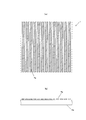
- FIG. 4 is an explanatory diagram ((a) is a plan view and (b) is a side view) showing a polarizer used in the polarized light irradiation apparatus for photo-alignment according to the embodiment of the present invention.
- the polarizer 4 is a wire grid type polarizer that is less dependent on the polarization characteristic with respect to the incident angle of light.
- This polarizer 4 has a plurality of grids 4g arranged in parallel on the surface of a substrate 4a that is transparent to light of a specific wavelength to be irradiated.
- the grid 4g is made of a linear electric conductor having a considerably long length with respect to the width, and is arranged in a plurality of rows in parallel at a predetermined pitch.
- the pitch of the grid 4g is appropriately set according to the wavelength of the polarized light.
- the material of the grid 4g is molybdenum silicon alloy (MoSix).
- MoSix molybdenum silicon alloy
- Aluminum (Al) or titanium oxide (TiOx) has been used as a grid material for wire grid polarizers.
- Aluminum grids have polarization characteristics in a relatively wide wavelength range, but are prone to deterioration due to oxidation and therefore require use in an anaerobic environment of oxygen.
- Titanium oxide grids are resistant to oxidation, but have polarization characteristics only in the wavelength range of about 240 nm to 300 nm, and therefore cannot be used at wavelengths of 300 nm or more.
- the polarizer 4 including the grid 4g made of molybdenum silicon alloy is not deteriorated due to oxidation, and can be sufficiently used in a clean room environment without an anaerobic environment. Moreover, since it has a polarization characteristic with respect to light in a wide wavelength range of 240 nm or more, it is possible to perform photo-alignment processing on various photosensitive material films having different photosensitive wavelengths.
- FIG. 5 is a graph showing the relationship between the wavelength of light incident on the polarizer and the extinction ratio.
- a polarizer made of a titanium oxide (TiOx) grid shows a characteristic that the peak is at a wavelength near 285 nm and the extinction ratio is lowered at a wavelength higher than that, and a polarization characteristic cannot be obtained near 360 nm. For this reason, it cannot be applied to an alignment film that performs light alignment treatment by irradiating light with a wavelength of 360 nm or more.
- An aluminum (Al) grid polarizer has a low extinction ratio in the wavelength range of 240 to 300 nm, and thus is difficult to apply to an alignment film that performs photo-alignment processing by irradiating light in the wavelength range in the vicinity.
- the polarizer 4 provided with the grid 4g made of molybdenum silicon alloy has an extinction ratio equivalent to that of the polarizer made of a titanium oxide grid in the wavelength region of 240 to 280 nm, and further in the wavelength region of 280 nm or more, aluminum.
- a higher extinction ratio can be obtained than a polarizer having a grid.
- the polarizer 4 including the grid 4g made of molybdenum silicon alloy can obtain high polarization characteristics in a wide wavelength range as compared with the polarizer made of titanium oxide or aluminum grid.
- 1 polarized light irradiation device for photo-alignment
- 2 light source
- 3 wavelength selection filter
- 4 Polarizer
- 4a substrate
- 4g grid
- 10 light irradiation unit
- 11 light source support guide
- 12 moving means
- 20 Substrate stage
- W Substrate
Landscapes
- Physics & Mathematics (AREA)
- Nonlinear Science (AREA)
- General Physics & Mathematics (AREA)
- Optics & Photonics (AREA)
- Chemical & Material Sciences (AREA)
- Crystallography & Structural Chemistry (AREA)
- Engineering & Computer Science (AREA)
- Manufacturing & Machinery (AREA)
- Spectroscopy & Molecular Physics (AREA)
- Mathematical Physics (AREA)
- Liquid Crystal (AREA)
- Polarising Elements (AREA)
Abstract
光配向用偏光照射装置における光源のメンテナンスを作業性良く、省スペースで行う。 光配向用偏光照射装置1は、光源2と偏光子4を含む光学部品とを備えた光照射部10を備え、光照射部10は、光源2を光学部品の上の光照射位置P1で支持すると共に光学部品から走査方向に離れたメンテナンス位置P2で支持する光源支持ガイド11を備え、光源支持ガイド11は、光照射位置P1からメンテナンス位置P2まで光源2を移動させる際に、光源2の向きを光照射側が走査方向に沿うように変更させる。
Description
本発明は、光配向処理に用いられる光配向用偏光照射装置に関するものである。
液晶素子の配向膜や紫外線硬化型液晶を用いた光学フィルムの配向層など、液晶分子を配向させる機能を有する膜や層(以下、総称して配向膜という)の形成に、近年、光配向処理が採用されている。光配向処理を行うには、配向膜となる感光性樹脂膜に選択された波長(例えば紫外光)の光を偏光軸が特定した偏光状態(例えば直線偏光状態)で照射する。
光配向処理用の偏光照射装置は、所定の幅を有する配向膜を連続的に形成するために、配向膜の幅方向に沿って棒状の光源(ロングアークランプ)を配置し、この光源と偏光子を組み合わせて、選択波長の偏光光を配向膜の幅方向に沿って照射し、これを配向膜の幅方向と交差する方向に走査するものが知られている(下記特許文献1参照)。
このような光配向用偏光照射装置は、所望の光照射強度や波長特性を維持するために長期間の使用に際して定期的に光源をメンテナンスすることが求められている。光源のメンテナンスには、ランプの交換や清掃が行われるが、ランプの下には偏光子などの光学部品が近接して配置されているので、ランプ交換等の作業性が悪く、また作業中に塵や結合部品などが光学部品上に落下することがあると、高価な光学部品を汚したり損傷したりする虞があった。
このような事態を避けるためには、光源全体を走査方向と交差する方向に引き出してメンテナンス作業を行うことも考えられる。しかしながら、液晶パネルの大型化などに伴い配向膜の幅は大きくなっており、その幅全体に配備される光源を幅方向に沿って走査領域の外側に引き出そうとすると、配向膜の幅と同等のスペースが走査領域の外側に必要になるので、光配向処理施設内部でのスペース確保が困難になる問題があった。
本発明は、このような問題に対処することを課題の一例とするものである。すなわち、光配向用偏光照射装置における光源のメンテナンスを作業性良く、省スペースで行うことができること、等が本発明の目的である。
このような目的を達成するために、本発明による光配向用偏光照射装置は、以下の構成を少なくとも具備するものである。
光源と偏光子を含む光学部品とを備えた光照射部を配向膜が形成される基板の幅方向に延設し、前記基板又は前記光照射部を前記基板の幅方向と交差する走査方向に沿って走査しながら前記基板上に特定波長の偏光光を照射する光配向用偏光照射装置であって、前記光照射部は、前記光源を前記光学部品の上の光照射位置で支持すると共に前記光学部品から前記走査方向に離れたメンテナンス位置で支持する光源支持ガイドを備え、前記光源支持ガイドは、前記光照射位置から前記メンテナンス位置まで前記光源を移動させる際に、前記光源の向きを光照射側が前記走査方向に沿うように変更させることを特徴とする光配向用偏光照射装置。
本発明は、このような特徴を備えることで、光学部品から走査方向に離れたメンテナンス位置に光源を移動させることができ、このメンテナンス位置では光源の向きを光照射側が走査方向に沿うように変更させることができるので、光配向用偏光照射装置における光源のメンテナンスを作業性良く、省スペースで行うことができる。
以下、図面を参照しながら本発明の実施形態を説明する。以下の図においては、走査方向をY方向、鉛直上向きをZ方向、走査方向及び鉛直上向きと直交する方向をX方向として示している。図1は本発明の一実施形態に係る光配向用偏光照射装置の全体構成を示した説明図である。
光配向用偏光照射装置1は、光照射部10と基板ステージ20を備える。光照射部10は、光源2と偏光子を含む光学部品を備えており、これらを配向膜が形成される基板Wの幅方向(図示X方向)に延設している。基板ステージ20には基板Wが載置される。光照射部10と基板ステージ20は走査方向Sに沿って相対的に移動する。これによって、光配向用偏光照射装置1は、基板W又は光照射部10を基板Wの幅方向と交差する走査方向Sに沿って走査しながら基板W上に特定波長の偏光光を照射する。
図1に示した例では、光照射部10の光源2は、ロングアークランプ2Pを備えている。ロングアークランプ2Pは、基板Wの幅方向全体に延設される長さを備えており、ロングアークランプ2Pの長手方向に交差する方向を走査方向にしている。
光照射部10は、光源2を支持する光源支持ガイド11を備えている。また、光照射部10は、光源2を光源支持ガイド11上で移動させる移動手段12を必要に応じて備えている。移動手段12は、電動シリンダ或いはモータなどで構成することができる。移動手段12を備えない場合には、光源2の光源支持ガイド11上での移動は手動によってなされる。
図2は、光源支持ガイドの具体的な構成を示した説明図である(図2(a)が平面図であり、図2(b)が光源の移動状態を示した側面図である。)。光源支持ガイド11は、光源2を光学部品(波長選択フィルタ3や偏光子4など)の上の光照射位置P1で支持すると共に、光学部品から走査方向(図示Y方向)に離れたメンテナンス位置P2で支持する。図示の例では、光源2はガイドローラ13を介して光源支持ガイド11に移動自在に支持されており、走査方向後方側のガイドローラ13Aが水平移動ガイド11A上に支持され、走査方向前方のガイドローラ13Bが傾斜移動ガイド11Bに支持されている。
基板Wを走査露光する通常の使用時には、光源2は光照射位置P1で光源支持ガイド11上に支持されており、この状態で光源2から出射された光は波長選択フィルタ3及び偏光子4を透過して基板W上に照射される。
光源2に対して交換等のメンテナンスを行う際には、光源支持ガイド11におけるメンテナンス位置P2まで光源2を移動させる。メンテナンス位置P2は、光照射位置P1に対して走査方向に離れた位置であり、波長選択フィルタ3や偏光子4などの光学部品上から離れた位置に設定される。
光源2を光照射位置P1からメンテナンス位置P2まで移動させる際に、走査方向後方のガイドローラ13Aが水平移動ガイド11A上を移動し、走査方向前方のガイドローラ13Bが傾斜移動ガイド11B上を移動することによって、光源2の向きは光照射側が走査方向に沿うように変更される。
図3は、形態が異なる光照射部の例を示している。図3(a)が平面図であり、図3(b)が光源の移動状態を示した側面図である。この例では、光照射部10の光源2は、複数の光源ユニット2Uが並列配置されている。光源ユニット2Uのそれぞれは短尺のロングアークランプ2P1を備えており、各ロングアークランプ2P1は、その長手方向を走査方向に向けて配置されている。また、並列配置されている光源ユニット2Uが複数段(2段)に配置されており、1段目の光源ユニット2Uと2段目の光源ユニット2Uの位置がシフトした位置に配置されている。
このような光源2を支持する光源支持ガイド11は、複数の光源ユニット2Uを一体に支持している。また、図示省略した移動手段は、複数の光源ユニット2Uを一体にして移動させる構成になっている。
図3に示した例も図2と同様の光源支持ガイド11を備えており、光源支持ガイド11は、光源2を光学部品(波長選択フィルタ3や偏光子4など)の上の光照射位置P1で支持すると共に、光学部品から走査方向(図示Y方向)に離れたメンテナンス位置P2で支持する。光源2はガイドローラ13を介して光源支持ガイド11に移動自在に支持されており、走査方向後方側のガイドローラ13Aが水平移動ガイド11A上に支持され、走査方向前方のガイドローラ13Bが傾斜移動ガイド11Bに支持されている。
そして、光源2を光照射位置P1からメンテナンス位置P2まで移動させる際に、走査方向後方のガイドローラ13Aが水平移動ガイド11A上を移動し、走査方向前方のガイドローラ13Bが傾斜移動ガイド11B上を移動することによって、光源2の向きは光照射側が走査方向に沿うように変更される。
以上説明したように、本発明の実施形態に係る光配向用偏光照射装置1によると、メンテナンス時に光源2のランプなどが走査方向正面に向けられることになるので、ランプ等の交換を容易に行うことができる。また、メンテナンス位置P2が設けられるスペースは、基板ステージ20を走査する際に必要となるスペースであるから、光配向用偏光照射装置1を設置するためのスペースとしては別途スペースを追加する必要が無い。これによって、省スペースで光源2のメンテナンス作業を行うことができる。
図4は、本発明の実施形態に係る光配向用偏光照射装置に用いられる偏光子を示した説明図((a)が平面図、(b)が側面図)である。偏光子4は、光源2にロングアークランプ2P,2P1を用いる場合には、光の入射角度に対する偏光特性の依存性が少ないワイヤーグリッド型偏光子が用いられる。この偏光子4は、照射する特定波長の光に対して透過性を有する基板4aの表面に複数のグリッド4gを並列配置したものである。グリッド4gは、幅に対して長さがかなり長い線状の電気導体からなり、これを所定のピッチで複数列平行に並べて配置したものである。グリッド4gのピッチは偏光する光の波長に応じて適宜設定される。
グリッド4gの材料はモリブデン珪素合金(MoSix)を用いる。従来、ワイヤーグリッド型偏光子のグリッド材料としては、アルミニウム(Al)や酸化チタン(TiOx)が用いられてきた。アルミニウム製のグリッドは、比較的広い波長域で偏光特性を有するが、酸化によって劣化し易いので酸素の嫌気的環境での使用が必要になる。酸化チタン製のグリッドは、酸化には強いが、約240nm~300nmの波長域でしか偏光特性を持たないため、300nm以上の波長での使用ができない問題がある。
これに対して、モリブデン珪素合金製のグリッド4gを備える偏光子4は、酸化による劣化がないので、嫌気的な環境下でないクリーンルーム環境で十分に使用が可能である。また、240nm以上の広い波長域の光に対して偏光特性を持っているので、感光波長の異なる様々な感光材料膜に対して光配向処理を施すことができる。
図5は、偏光子に入射する光の波長と消光比の関係を示したグラフである。酸化チタン(TiOx)製グリッドの偏光子は285nm付近の波長をピークとしてそれ以上の波長では消光比が低下する特性を示し、360nm付近では偏光特性が得られなくなる。このため、360nm以上の波長の光を照射して光配向処理を行う配向膜には適用できない。アルミニウム(Al)製グリッドの偏光子は240~300nmの波長域では消光比が低いので、この付近の波長域の光を照射して光配向処理を行う配向膜には適用しにくい。これに対して、モリブデン珪素合金製のグリッド4gを備える偏光子4は、240~280nmの波長域で酸化チタン製グリッドの偏光子と同等の消光比が得られ、更に280nm以上の波長域ではアルミニウム製グリッドを有する偏光子よりも高い消光比が得られる。このように、モリブデン珪素合金製のグリッド4gを備える偏光子4は、広い波長域で酸化チタン製やアルミニウム製グリッドの偏光子と比較して高い偏光特性を得ることができる。
以上、本発明の実施の形態について図面を参照して詳述してきたが、具体的な構成はこれらの実施の形態に限られるものではなく、本発明の要旨を逸脱しない範囲の設計の変更等があっても本発明に含まれる。また、上述の各実施の形態は、その目的及び構成等に特に矛盾や問題がない限り、互いの技術を流用して組み合わせることが可能である。
1:光配向用偏光照射装置,2:光源,3:波長選択フィルタ,
4:偏光子,4a:基板,4g:グリッド,
10:光照射部,11:光源支持ガイド,12:移動手段,
20:基板ステージ,W:基板
4:偏光子,4a:基板,4g:グリッド,
10:光照射部,11:光源支持ガイド,12:移動手段,
20:基板ステージ,W:基板
Claims (4)
- 光源と偏光子を含む光学部品とを備えた光照射部を配向膜が形成される基板の幅方向に延設し、前記基板又は前記光照射部を前記基板の幅方向と交差する走査方向に沿って走査しながら前記基板上に特定波長の偏光光を照射する光配向用偏光照射装置であって、
前記光照射部は、
前記光源を前記光学部品の上の光照射位置で支持すると共に前記光学部品から前記走査方向に離れたメンテナンス位置で支持する光源支持ガイドを備え、
前記光源支持ガイドは、前記光照射位置から前記メンテナンス位置まで前記光源を移動させる際に、前記光源の向きを光照射側が前記走査方向に沿うように変更させることを特徴とする光配向用偏光照射装置。 - 前記光照射部は、前記光源を前記光照射位置から前記メンテナンス位置まで移動させる移動手段を備えることを特徴とする請求項1に記載の光配向用偏光照射装置。
- 前記光源は複数の光源ユニットが並列配置されており、
前記光源支持ガイドは、複数の前記光源ユニットを一体に支持し、
前記移動手段は、複数の前記光源ユニットを一体にして移動させることを特徴とする請求項2記載の光配向用偏光照射装置。 - 前記偏光子は、複数のグリッドを並列配置したワイヤーグリッド型偏光子であり、前記グリッドがモリブデン珪素合金で形成されていることを特徴とする請求項1~3のいずれかに記載された光配向用偏光照射装置。
Priority Applications (2)
| Application Number | Priority Date | Filing Date | Title |
|---|---|---|---|
| CN201480009344.7A CN105008990B (zh) | 2013-03-07 | 2014-03-07 | 光取向用偏光照射装置 |
| KR1020157023876A KR20150127064A (ko) | 2013-03-07 | 2014-03-07 | 광배향용 편광 조사 장치 |
Applications Claiming Priority (4)
| Application Number | Priority Date | Filing Date | Title |
|---|---|---|---|
| JP2013045995 | 2013-03-07 | ||
| JP2013-045995 | 2013-03-07 | ||
| JP2014044257A JP6308816B2 (ja) | 2013-03-07 | 2014-03-06 | 光配向用偏光照射装置 |
| JP2014-044257 | 2014-03-06 |
Publications (1)
| Publication Number | Publication Date |
|---|---|
| WO2014136934A1 true WO2014136934A1 (ja) | 2014-09-12 |
Family
ID=51491441
Family Applications (1)
| Application Number | Title | Priority Date | Filing Date |
|---|---|---|---|
| PCT/JP2014/055945 Ceased WO2014136934A1 (ja) | 2013-03-07 | 2014-03-07 | 光配向用偏光照射装置 |
Country Status (4)
| Country | Link |
|---|---|
| JP (1) | JP6308816B2 (ja) |
| KR (1) | KR20150127064A (ja) |
| CN (1) | CN105008990B (ja) |
| WO (1) | WO2014136934A1 (ja) |
Cited By (3)
| Publication number | Priority date | Publication date | Assignee | Title |
|---|---|---|---|---|
| JP2015118369A (ja) * | 2013-11-13 | 2015-06-25 | 大日本印刷株式会社 | 偏光子、偏光子用基板および光配向装置 |
| JP2015135459A (ja) * | 2013-12-20 | 2015-07-27 | 大日本印刷株式会社 | 偏光子および光配向装置 |
| JPWO2015108075A1 (ja) * | 2014-01-15 | 2017-03-23 | 大日本印刷株式会社 | 偏光子、偏光子の製造方法、光配向装置および偏光子の装着方法 |
Families Citing this family (5)
| Publication number | Priority date | Publication date | Assignee | Title |
|---|---|---|---|---|
| JP6554768B2 (ja) * | 2014-07-08 | 2019-08-07 | 大日本印刷株式会社 | 偏光子、積層基板、および光配向装置 |
| JP6884501B2 (ja) * | 2015-08-25 | 2021-06-09 | 大日本印刷株式会社 | 偏光子 |
| JP6575292B2 (ja) * | 2015-10-20 | 2019-09-18 | ウシオ電機株式会社 | 光照射装置 |
| JP6870391B2 (ja) * | 2017-03-06 | 2021-05-12 | ウシオ電機株式会社 | 光照射装置 |
| CN110554536B (zh) * | 2018-05-31 | 2025-05-27 | 上海微电子装备(集团)股份有限公司 | 一种光配向设备以及光配向设备中灯管的更换方法 |
Citations (4)
| Publication number | Priority date | Publication date | Assignee | Title |
|---|---|---|---|---|
| US20040212790A1 (en) * | 2003-04-24 | 2004-10-28 | Eastman Kodak Company | Optical exposure apparatus for forming an alignment layer |
| JP2006133498A (ja) * | 2004-11-05 | 2006-05-25 | Ushio Inc | 光配向用偏光光照射装置 |
| JP2006323060A (ja) * | 2005-05-18 | 2006-11-30 | Ushio Inc | 偏光光照射装置 |
| JP2010501085A (ja) * | 2006-08-15 | 2010-01-14 | エーピーアイ ナノファブリケーション アンド リサーチ コーポレーション | 偏光子薄膜及びこの製作方法 |
Family Cites Families (4)
| Publication number | Priority date | Publication date | Assignee | Title |
|---|---|---|---|---|
| JP3540174B2 (ja) * | 1998-10-12 | 2004-07-07 | ウシオ電機株式会社 | 斜めから光を照射するプロキシミティ露光方法 |
| JP4506412B2 (ja) * | 2004-10-28 | 2010-07-21 | ウシオ電機株式会社 | 偏光素子ユニット及び偏光光照射装置 |
| WO2008022097A2 (en) * | 2006-08-15 | 2008-02-21 | Api Nanofabrication And Research Corp. | Methods for forming patterned structures |
| JP5607104B2 (ja) * | 2012-04-25 | 2014-10-15 | 岩崎電気株式会社 | 偏光紫外線照射装置 |
-
2014
- 2014-03-06 JP JP2014044257A patent/JP6308816B2/ja active Active
- 2014-03-07 KR KR1020157023876A patent/KR20150127064A/ko not_active Withdrawn
- 2014-03-07 CN CN201480009344.7A patent/CN105008990B/zh active Active
- 2014-03-07 WO PCT/JP2014/055945 patent/WO2014136934A1/ja not_active Ceased
Patent Citations (4)
| Publication number | Priority date | Publication date | Assignee | Title |
|---|---|---|---|---|
| US20040212790A1 (en) * | 2003-04-24 | 2004-10-28 | Eastman Kodak Company | Optical exposure apparatus for forming an alignment layer |
| JP2006133498A (ja) * | 2004-11-05 | 2006-05-25 | Ushio Inc | 光配向用偏光光照射装置 |
| JP2006323060A (ja) * | 2005-05-18 | 2006-11-30 | Ushio Inc | 偏光光照射装置 |
| JP2010501085A (ja) * | 2006-08-15 | 2010-01-14 | エーピーアイ ナノファブリケーション アンド リサーチ コーポレーション | 偏光子薄膜及びこの製作方法 |
Cited By (3)
| Publication number | Priority date | Publication date | Assignee | Title |
|---|---|---|---|---|
| JP2015118369A (ja) * | 2013-11-13 | 2015-06-25 | 大日本印刷株式会社 | 偏光子、偏光子用基板および光配向装置 |
| JP2015135459A (ja) * | 2013-12-20 | 2015-07-27 | 大日本印刷株式会社 | 偏光子および光配向装置 |
| JPWO2015108075A1 (ja) * | 2014-01-15 | 2017-03-23 | 大日本印刷株式会社 | 偏光子、偏光子の製造方法、光配向装置および偏光子の装着方法 |
Also Published As
| Publication number | Publication date |
|---|---|
| CN105008990B (zh) | 2018-03-30 |
| KR20150127064A (ko) | 2015-11-16 |
| JP2014197189A (ja) | 2014-10-16 |
| CN105008990A (zh) | 2015-10-28 |
| JP6308816B2 (ja) | 2018-04-11 |
Similar Documents
| Publication | Publication Date | Title |
|---|---|---|
| JP6308816B2 (ja) | 光配向用偏光照射装置 | |
| CN101566762B (zh) | 光取向用偏振光照射装置 | |
| JP4815995B2 (ja) | 光配向用偏光光照射装置 | |
| CN100495164C (zh) | 光取向用偏振光照射装置 | |
| JP5077465B2 (ja) | 光配向用偏光光照射装置 | |
| CN203720500U (zh) | 光取向用偏振照射装置 | |
| CN104395831B (zh) | 曝光装置 | |
| TWI553385B (zh) | 光配向處理裝置 | |
| TWI521258B (zh) | 光配向照射裝置 | |
| JP2015004896A (ja) | 光配向用偏光光照射装置及び光配向用偏光光照射方法 | |
| TWI606287B (zh) | 紫外線照射裝置 | |
| JP2014153371A (ja) | レーザリペア装置 | |
| JP2015106015A (ja) | 偏光光照射装置、偏光光照射方法および偏光光照射プログラム | |
| JP6500543B2 (ja) | 偏光子、光配向装置、および光配向方法 | |
| KR20130088369A (ko) | 마스크 처짐을 개선한 노광 장치 | |
| KR20120060483A (ko) | 자외선-오존을 이용한 오염물 세정장치 및 이를 이용한 세정방법 | |
| CN104834129A (zh) | 液晶显示装置的制造方法和制造装置 | |
| CN109212837B (zh) | 一种光配向装置及方法 | |
| JP7035376B2 (ja) | 偏光光照射装置および偏光光照射方法 | |
| JP6534567B2 (ja) | 光照射装置 | |
| JP6870391B2 (ja) | 光照射装置 | |
| JP6253002B2 (ja) | 光配向用偏光光照射装置及び光配向用偏光光照射方法 | |
| CN115586673A (zh) | 偏振光照射装置、具备其的曝光装置以及偏振光照射方法 | |
| CN204101765U (zh) | 偏光元件单元以及使用偏光元件单元的偏光照射装置 | |
| JP5979179B2 (ja) | 偏光光照射装置 |
Legal Events
| Date | Code | Title | Description |
|---|---|---|---|
| 121 | Ep: the epo has been informed by wipo that ep was designated in this application |
Ref document number: 14761143 Country of ref document: EP Kind code of ref document: A1 |
|
| ENP | Entry into the national phase |
Ref document number: 20157023876 Country of ref document: KR Kind code of ref document: A |
|
| NENP | Non-entry into the national phase |
Ref country code: DE |
|
| 122 | Ep: pct application non-entry in european phase |
Ref document number: 14761143 Country of ref document: EP Kind code of ref document: A1 |