WO2014136393A1 - 加工基板及びそれを用いた半導体装置 - Google Patents
加工基板及びそれを用いた半導体装置 Download PDFInfo
- Publication number
- WO2014136393A1 WO2014136393A1 PCT/JP2014/000897 JP2014000897W WO2014136393A1 WO 2014136393 A1 WO2014136393 A1 WO 2014136393A1 JP 2014000897 W JP2014000897 W JP 2014000897W WO 2014136393 A1 WO2014136393 A1 WO 2014136393A1
- Authority
- WO
- WIPO (PCT)
- Prior art keywords
- processed substrate
- equilateral triangle
- protrusions
- substrate
- gan
- Prior art date
- Legal status (The legal status is an assumption and is not a legal conclusion. Google has not performed a legal analysis and makes no representation as to the accuracy of the status listed.)
- Ceased
Links
Images





Classifications
-
- C—CHEMISTRY; METALLURGY
- C30—CRYSTAL GROWTH
- C30B—SINGLE-CRYSTAL GROWTH; UNIDIRECTIONAL SOLIDIFICATION OF EUTECTIC MATERIAL OR UNIDIRECTIONAL DEMIXING OF EUTECTOID MATERIAL; REFINING BY ZONE-MELTING OF MATERIAL; PRODUCTION OF A HOMOGENEOUS POLYCRYSTALLINE MATERIAL WITH DEFINED STRUCTURE; SINGLE CRYSTALS OR HOMOGENEOUS POLYCRYSTALLINE MATERIAL WITH DEFINED STRUCTURE; AFTER-TREATMENT OF SINGLE CRYSTALS OR A HOMOGENEOUS POLYCRYSTALLINE MATERIAL WITH DEFINED STRUCTURE; APPARATUS THEREFOR
- C30B29/00—Single crystals or homogeneous polycrystalline material with defined structure characterised by the material or by their shape
- C30B29/10—Inorganic compounds or compositions
- C30B29/40—AIIIBV compounds wherein A is B, Al, Ga, In or Tl and B is N, P, As, Sb or Bi
- C30B29/403—AIII-nitrides
- C30B29/406—Gallium nitride
-
- C—CHEMISTRY; METALLURGY
- C30—CRYSTAL GROWTH
- C30B—SINGLE-CRYSTAL GROWTH; UNIDIRECTIONAL SOLIDIFICATION OF EUTECTIC MATERIAL OR UNIDIRECTIONAL DEMIXING OF EUTECTOID MATERIAL; REFINING BY ZONE-MELTING OF MATERIAL; PRODUCTION OF A HOMOGENEOUS POLYCRYSTALLINE MATERIAL WITH DEFINED STRUCTURE; SINGLE CRYSTALS OR HOMOGENEOUS POLYCRYSTALLINE MATERIAL WITH DEFINED STRUCTURE; AFTER-TREATMENT OF SINGLE CRYSTALS OR A HOMOGENEOUS POLYCRYSTALLINE MATERIAL WITH DEFINED STRUCTURE; APPARATUS THEREFOR
- C30B25/00—Single-crystal growth by chemical reaction of reactive gases, e.g. chemical vapour-deposition growth
- C30B25/02—Epitaxial-layer growth
- C30B25/18—Epitaxial-layer growth characterised by the substrate
- C30B25/186—Epitaxial-layer growth characterised by the substrate being specially pre-treated by, e.g. chemical or physical means
-
- H—ELECTRICITY
- H10—SEMICONDUCTOR DEVICES; ELECTRIC SOLID-STATE DEVICES NOT OTHERWISE PROVIDED FOR
- H10H—INORGANIC LIGHT-EMITTING SEMICONDUCTOR DEVICES HAVING POTENTIAL BARRIERS
- H10H20/00—Individual inorganic light-emitting semiconductor devices having potential barriers, e.g. light-emitting diodes [LED]
- H10H20/80—Constructional details
- H10H20/81—Bodies
- H10H20/819—Bodies characterised by their shape, e.g. curved or truncated substrates
- H10H20/82—Roughened surfaces, e.g. at the interface between epitaxial layers
-
- H—ELECTRICITY
- H10—SEMICONDUCTOR DEVICES; ELECTRIC SOLID-STATE DEVICES NOT OTHERWISE PROVIDED FOR
- H10H—INORGANIC LIGHT-EMITTING SEMICONDUCTOR DEVICES HAVING POTENTIAL BARRIERS
- H10H20/00—Individual inorganic light-emitting semiconductor devices having potential barriers, e.g. light-emitting diodes [LED]
- H10H20/80—Constructional details
- H10H20/81—Bodies
- H10H20/822—Materials of the light-emitting regions
- H10H20/824—Materials of the light-emitting regions comprising only Group III-V materials, e.g. GaP
- H10H20/825—Materials of the light-emitting regions comprising only Group III-V materials, e.g. GaP containing nitrogen, e.g. GaN
Definitions
- the present invention relates to a processed substrate and a semiconductor device using the processed substrate.
- a semiconductor layer having a nonpolar surface can be crystal-grown on the substrate, and dislocations of the semiconductor layer to be crystal-grown on the substrate can be reduced. It has been known.
- Patent Document 1 discloses a processed substrate in which a crystal growth surface of a sapphire substrate has an irregular structure by etching or the like.
- Non-Patent Document 1 discloses a processed substrate in which a plurality of randomly arranged cone-shaped protrusions are formed on the substrate surface.
- the present invention is a processed substrate in which a plurality of protrusions arranged to form an equilateral triangular lattice in a plan view are formed on a substrate surface, and a GaN crystal whose principal surface is c-plane can be grown on the substrate.
- the plurality of protrusions are arranged such that three sides of an equilateral triangle in an equilateral triangular lattice constituted by the plurality of protrusions are relative to the a-axis of GaN when GaN whose principal surface is c-plane is grown on the substrate.
- the smallest angle is 10 to 50 °.
- a processed substrate having a plurality of protrusions formed so as to form an equilateral triangular lattice in a plan view is formed on the surface of the substrate, and a GaN crystal whose principal surface is c-plane is grown on the processed substrate.
- a plurality of protrusions of the processed substrate, wherein three sides of an equilateral triangle in an equilateral triangle lattice constituted by the plurality of protrusions are formed on the GaN layer.
- the smallest angle is arranged to be 10 to 50 °.
- FIG. 1 is a longitudinal sectional view of a semiconductor light emitting device according to an embodiment. It is a top view of a part of a processed substrate.
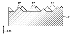
- FIG. 3 is a sectional view taken along line III-III in FIG. 2.
- (A) is the 1st longitudinal cross-sectional view which shows the preparation methods of a wafer processing board
- (A) is the 2nd longitudinal cross-sectional view which shows the preparation methods of a wafer processing board
- A)-(d) is explanatory drawing which shows the manufacturing method of the semiconductor light-emitting device based on Embodiment.
- FIG. 1 shows a semiconductor light emitting device 10 according to an embodiment.
- the u-GaN layer 13, the n-type GaN layer 14, the multiple quantum well layer 15, and the p-type GaN layer 16 are sequentially stacked on the processing substrate 11, and An n-type electrode 17 is provided on the n-type GaN layer 14 exposed by etching, and a p-type electrode 18 is provided on the p-type GaN layer 16, for example, used as a light emitting diode It is.
- 2 and 3 show the processed substrate 11.
- 2 and 3 show crystal plane orientations using a sapphire processed substrate whose main surface is a-plane as an example (the same applies to FIGS. 4 and 5 below).
- the processed substrate 11 is capable of crystal growth of GaN having a c-plane main surface on the substrate.
- the processed substrate 11 include a sapphire processed substrate (PSS: Patterned Sapphire Substrate), a Si processed substrate, and a SiC processed substrate. More specifically, the main surface has a c-plane sapphire processed substrate, a-plane sapphire substrate, main surface is n-plane sapphire substrate, main surface is (111) Si substrate, main surface is (110) Si substrate, 3C-SiC substrate, 4C-SiC Examples thereof include a processed substrate, a 6H—SiC processed substrate, and a SiC processed substrate having a c-plane main surface.
- a sapphire processed substrate having a c-plane principal surface is preferable.
- the processed substrate 11 is formed in a rectangular plate shape in the state of the semiconductor light emitting element 10, and in this case, the vertical and horizontal dimensions are 200 to 1000 ⁇ m, and the thickness is 50 to 300 ⁇ m.
- a plurality of protrusions 12 are formed on the substrate surface of the processed substrate 11.
- Examples of the shape of the protrusion 12 include a pyramid, a truncated cone, a truncated pyramid, a cylinder, a prism, and a hemisphere in addition to the cone shown in FIGS.
- the shape of the protrusion 12 preferably has a side surface that is inclined with respect to the main surface of the processed substrate 11. From this viewpoint, a cone, a pyramid, a truncated cone, a truncated pyramid, and a hemisphere are preferable.
- the shape of the projection 12 is preferably a curved surface formed in the circumferential direction and having a side surface with a continuously changing crystal plane.
- the shape of the protrusion 12 is preferably a cone, a truncated cone, or a hemisphere, and a cone is particularly preferable.
- the “cone” and the “conical frustum” in the present application include those in which a contour of a side surface in a side view is a curved curve bulging outward.
- the shape of the some protrusion 12 is the same, the thing from which a shape differs may be mixed.
- the maximum outer diameter of the protrusion 12 (in the case of the conical protrusion 12, the diameter of the bottom surface) is preferably 1 ⁇ m or more, more preferably 2 ⁇ m or more.
- the height of the protrusion 12 is preferably 0.5 ⁇ m or more, more preferably 1.5 ⁇ m or more.
- the maximum outer diameter of the protrusion 12 is preferably larger than the height of the protrusion 12.
- the dimension structure of the some protrusion 12 is the same, the thing from which a dimension structure differs may be mixed.
- the plurality of protrusions 12 are arranged so as to form an equilateral triangular lattice in a plan view. That is, an equilateral triangular lattice is formed by combining the positions of the centers of gravity of the projections 12 in the plan view.
- the length of one side of the equilateral triangle in the equilateral triangle lattice is preferably 2 ⁇ m or more, more preferably 3 ⁇ m or more.
- the length of one side of the equilateral triangle is larger than the maximum outer diameter of the projection 12, and therefore, the pair of projections 12 at the two vertices included in the same equilateral triangle are arranged with a space between each other. .
- the interval is, for example, 0.1 to 2.0 ⁇ m.
- the plurality of protrusions 12 have crystal growth of GaN whose three sides of the equilateral triangle in the equilateral triangular lattice formed by the plurality of protrusions 12 are c-plane on the processed substrate 10.
- the a-axis of GaN that is, the normal axis of the a-plane (in the case of the sapphire processed substrate 11 whose main surface is the c-plane, the m-axis on the main surface of the sapphire processed substrate, that is, the normal axis of the m-plane)
- the smallest angle ⁇ among the angles ⁇ counterclockwise is 10 to 50 °.
- This smallest angle ⁇ is preferably 20 ° or more and preferably 40 ° or less from the viewpoint of the effect of reducing the dislocation density of the semiconductor layer 13 formed on the processed substrate 11 described later. Most preferably, this smallest angle ⁇ is 30 °. It should be noted that the three sides of the equilateral triangle change every 60 ° with the side having the smallest angle ⁇ counterclockwise with respect to the a-axis of GaN. The above conditions for the processed substrate 11 are 10 ° ⁇ ⁇ ⁇ 50 °.
- the arrangement density of the plurality of protrusions 12 is preferably 1 ⁇ 10 6 pieces / cm 2 or more, more preferably 1 ⁇ 10 7 pieces / cm 2 or more.
- the exclusive area ratio of the main surface portion excluding the protrusions 12 in a plan view of the substrate surface of the processed substrate 11 is preferably 70% or less, more preferably 55% or less.
- the constituent material of the u-GaN layer 13 is undoped GaN that is not doped with a dopant.
- the u-GaN layer 13 is formed by crystal growth of GaN starting from a crystal plane included in the substrate surface on the processed substrate 11, and the main surface is a c-plane.
- the thickness of the u-GaN layer 13 is, for example, 2 to 20 ⁇ m.
- the processed substrate 11 is such that GaN whose principal surface is c-plane can grow on the substrate, and is disposed on the substrate surface so as to form an equilateral triangular lattice in plan view.
- the plurality of protrusions 12 are formed, and the plurality of protrusions 12 are formed of GaN whose three sides of an equilateral triangle in the equilateral triangle lattice formed by them are c-plane GaN on the processed substrate 10. Is formed on the processed substrate 11 by arranging the smallest angle of 10 to 50 ° among the angles formed counterclockwise with respect to the a-axis of GaN when the crystal grows.
- the dislocation density of the u-GaN layer 13 is reduced.
- the dark spot density on the surface of the u-GaN layer 13 measured by the cathodoluminescence (CL) method is 1.15 ⁇ 10 8 pieces / cm 2 or less.
- the number is preferably 1.00 ⁇ 10 8 pieces / cm 2 or less, and more preferably 9.90 ⁇ 10 7 pieces / cm 2 or less.
- a low-temperature buffer layer having a thickness of about 20 to 30 nm may be provided between the processed substrate 11 and the u-GaN layer 13.
- the constituent material of the n-type GaN layer 14 is GaN doped with an n-type dopant.
- the n-type dopant include Si and Ge.
- the concentration of the n-type dopant is, for example, 1.0 ⁇ 10 17 to 20 ⁇ 10 17 / cm 3 .
- the n-type GaN layer 14 may be composed of a single layer, or may be composed of a plurality of layers having different n-type dopant types and concentrations.
- the thickness of the n-type GaN layer 14 is 2 to 10 ⁇ m, for example.
- the multiple quantum well layer 15 has an alternate stacked structure of well layers 15a and barrier layers 15b.
- the number of well layers 15a and barrier layers 15b is, for example, 5 to 15.
- Examples of the constituent material of the well layer 15a include InGaN and InGaAlN.
- the thickness of the well layer 15a is, for example, 1 to 20 nm.
- Examples of the constituent material of the barrier layer 15b include GaN, InGaN (however, larger than the band gap of the well layer 15a).
- the thickness of the barrier layer 15b is, for example, 5 to 20 nm.
- the constituent material of the p-type GaN layer 16 is GaN doped with a p-type dopant.
- the p-type dopant include Mg and Cd.
- the free hole concentration measured by the Hall effect measurement is, for example, 2.0 ⁇ 10 17 to 10 ⁇ 10 17 / cm 3 .
- the p-type GaN layer 16 may be composed of a single layer, or may be composed of a plurality of layers having different types and concentrations of the p-type dopant.
- the thickness of the p-type GaN layer 16 is, for example, 50 to 200 nm.
- n-type electrode 17 examples include a laminated structure such as Ti / Al, Ti / Al / Mo / Au, and Hf / Au, or an alloy.
- the thickness of the n-type electrode 17 is, for example, 10 nm / 500 nm in the laminated structure of Ti / Al.
- Examples of the p-type electrode 18 include a laminated structure such as Pd / Pt / Au, Ni / Au, and Pd / Mo / Au, an alloy, or an oxide-based transparent conductive material such as ITO (indium tin oxide). It is done.
- the thickness of the p-type electrode 18 is 10 to 200 nm for ITO, for example.
- the processed substrate 11 is capable of crystal growth of GaN having a c-plane main surface on the substrate, and is positive on the substrate surface in plan view.
- a plurality of projections 12 are formed so as to form a triangular lattice, and the three sides of the regular triangle in the regular triangular lattice constituted by the plurality of projections 12 are formed on the processed substrate 10.
- the smallest angle among the angles formed counterclockwise with respect to the a-axis of GaN when the GaN crystal having the c-plane principal surface is grown is 10 to 50 °
- the dislocation density of the u-GaN layer 13 which is a semiconductor layer formed on the processed substrate 11 is reduced, and accordingly, the n-type GaN layer 14, the multiple quantum well layer 15, and the p-type GaN layer formed thereon. 16 semiconductors It becomes the crystallinity of the layer is excellent. As a result, it is possible to improve the luminous efficiency.
- a wafer processed substrate 11 ′ (processed substrate 11) is manufactured, and a u-GaN layer 13, an n-type GaN layer 14 (Si-doped), and a light emitting layer are formed thereon.
- the multiple quantum well layer 15 well layer 15a: InGaN, barrier layer 15b: GaN
- the p-type GaN layer 16 (Mg doped) are formed in order
- the n-type GaN layer 14 and the p-type GaN layer 16 are formed.
- the n-type electrode 17 and the p-type electrode 18 are formed respectively.
- a wafer W having a c-plane main surface is prepared.
- the wafer W has a thickness of 0.3 to 3.0 mm and a diameter of 50 to 300 mm, although it varies depending on the diameter. In the case of a wafer W having a diameter of 50 mm, 5000 to 12000 semiconductor light emitting elements 10 can be formed on one wafer W.
- a protrusion 12 is formed on the surface of the wafer W to produce a wafer processing substrate 11 '.
- an equilateral triangular lattice is formed on the surface of the wafer W by the photoresist R by a photolithography process.
- the sapphire processed substrate 11 in which the three sides of the equilateral triangle are grown on the surface of the wafer W, and the GaN having the c-plane as the main surface is grown on the surface.
- the angles formed counterclockwise with respect to the m-axis on the main surface of the sapphire substrate a plurality of dots arranged so that the smallest angle is 10 to 50 ° is patterned. This angle can be arbitrarily set by rotating the wafer W in-plane with respect to the fixed photomask.
- the photoresist R a positive type can be suitably used.
- the diameter of the dot of the photoresist R is, for example, 0.5 to 4 ⁇ m and the thickness is 0.5 to 4 ⁇ m, for example, although it depends on the size of the projection 12 to be formed.
- the inter-dot distance of the photoresist R is, for example, 0.5 to 4 ⁇ m although it depends on the size of the projection 12 to be formed.
- the photoresist R is pre-baked before exposure / development and post-baked after exposure / development.
- the pre-baking and post-baking temperatures are, for example, 80 to 130 ° C. In post-baking, the dots of the photoresist R may be thermally deformed into a dome shape by setting the temperature higher.
- the surface of the wafer W is subjected to reactive ion etching by inductively coupled plasma (Inductive Coupled Plasma Reactive Ion Etching).
- the protrusion 12 is formed by etching.
- the portion of the surface of the wafer W where the photoresist R is not provided is etched, while the portion where the photoresist R is provided remains and is formed on the protrusion 12. If the etching conditions are adjusted, the photo The frustoconical protrusions 12 with the resist R remaining on the top surface can be formed, or the conical protrusions 12 can be formed by etching enough to remove the photoresist R.
- the etching time is, for example, 1 to 30 minutes.
- the antenna power is, for example, 100 to 1000 W
- the bias power is, for example, 50 to 500 W.
- the pressure is, for example, 0.05 to 0.8 Pa.
- As the etching gas various halogen-based gases such as Cl 2 and BCl 3 and Ar gas can be used.
- MOVPE metal organic vapor phase epitaxy
- MBE molecular beam epitaxy
- HVPE hydride vapor phase epitaxy
- metalorganic vapor phase epitaxy is the most common.
- the MOVPE apparatus used for forming the u-GaN layer 13 and the like includes a wafer transfer system, a wafer heating system, a gas supply system, and a gas exhaust system that are electronically controlled.
- the wafer heating system is composed of a thermocouple, a resistance heater, and a carbon or SiC susceptor provided thereon.
- the MOVPE apparatus is configured to grow a semiconductor crystal with a reactive gas on a wafer processing substrate 11 ′ set on a susceptor of a quartz tray to be conveyed.
- the wafer processing substrate 11 ′ having the protrusions 12 is set on the quartz tray so that the surface on which the protrusions 12 are formed faces upward, and then the wafer processing substrate 11 ′ is 1050 to 1150 ° C.
- the pressure in the reaction vessel is set to 10 to 100 kPa, and H 2 is circulated as a carrier gas in a flow channel installed in the reaction vessel, and this state is maintained for several minutes to maintain the wafer processing substrate 11 ′. Perform thermal cleaning.
- the temperature of the wafer processing substrate 11 ′ is set to 1050 to 1150 ° C.
- the pressure in the reaction vessel is set to 10 to 100 kPa
- the carrier gas H 2 is set to 10 slm (slm is 25 ° C. and 1 atm at 1 atmosphere).
- a group V element supply source (NH 3 ) and a group III element supply source (TMG) are supplied as reaction gases to the respective supply flow rates of 0.1 to The flow rate is 5 slm and 50 to 150 ⁇ mol / min.
- undoped GaN grows on the substrate surface of the wafer processing substrate 11 ′, and as shown in FIG. 6A, the u-GaN layer 13 whose principal surface is the c-plane is formed on the wafer processing substrate 11 ′. It is formed.
- a low-temperature buffer layer may be formed on the wafer processing substrate 11 ′ before forming the u-GaN layer 13.
- the temperature of the wafer processing substrate 11 ′ is set to 400 to 500 ° C., and GaN is crystal-grown. Just do it.
- n-type GaN layer- The pressure in the reaction vessel is set to 10 to 100 kPa, and the carrier gas H 2 is circulated in the reaction vessel at a flow rate of 5 to 15 slm, and there as a reaction gas, a group V element supply source (NH 3 ), a group III Element supply source 1 (TMG) and n-type doping element supply source (SiH 4 ) are supplied at a supply flow rate of 0.1 to 5 slm, 50 to 150 ⁇ mol / min, and 1 to 5 ⁇ 10 ⁇ 3 ⁇ mol / min, respectively. Let it flow.
- NH 3 group V element supply source
- TMG group III Element supply source 1
- SiH 4 n-type doping element supply source
- the n-type GaN crystal grows continuously on the u-GaN layer 13 to form the n-type GaN layer 14.
- the temperature of the wafer processing substrate 11 ′ is set to about 800 ° C.
- the pressure in the reaction vessel is set to 10 to 100 kPa
- the carrier gas N 2 is allowed to flow through the reaction vessel at a flow rate of 5 to 15 slm, and as a reaction gas there.
- Group V element supply source (NH 3 ), Group III element supply source 1 (TMG), and Group III element supply source 2 (TMI) are supplied at a flow rate of 0.1 to 5 slm, 5 to 15 ⁇ mol / min, And 2 to 30 ⁇ mol / min.
- InGaN crystal grows continuously on the n-type GaN layer 14 to form the well layer 15a.
- a group V element supply source (NH 3 ) and a group III element supply source (TMG) are flowed so that the respective supply flow rates are 0.1 to 5 slm and 5 to 15 ⁇ mol / min.
- NH 3 group V element supply source
- TMG group III element supply source
- the multiple quantum well layer 15 is formed by alternately forming the well layers 15a and the barrier layers 15b as shown in FIG. 6C.
- the emission wavelength of the multiple quantum well layer 15 depends on the well width of the well layer 15a (the thickness of the well layer 15a) and the InN mixed crystal ratio, and the higher the InN mixed crystal ratio, the longer the emission wavelength.
- the InN mixed crystal ratio is determined by the TMI molar flow rate / (TMG molar flow rate + TMI molar flow rate) and the growth temperature.
- the temperature of the wafer processing substrate 11 ′ is set to 1000 to 1100 ° C.
- the pressure in the reaction vessel is set to 10 to 100 kPa
- the carrier gas H 2 is circulated in the reaction vessel at a flow rate of 5 to 15 slm.
- a group V element supply source (NH 3 ), a group III element supply source 1 (TMG), and a p-type doping element supply source (Cp 2 Mg) are supplied at a supply flow rate of 0.1 to 5 slm, 50 It is made to flow so that it may become -150 micromol / min and 0.03-30 micromol / min.
- the p-type GaN crystal grows continuously on the multiple quantum well layer 15 to form the p-type GaN layer 16.
- n-type GaN layer 14 is exposed by partially reactive ion etching the wafer processing substrate 11 'on which the u-GaN layer 13 and the like are laminated, vacuum deposition, sputtering, CVD (Chemical Vapor Deposition), etc.
- the n-type electrode 17 and the p-type electrode 18 are formed on the n-type GaN layer 14 and the p-type GaN layer 16, respectively.
- the wafer processing substrate 11 ′ is cleaved to be divided into individual semiconductor light emitting elements 10.
- the semiconductor light emitting element 10 is used as an example.
- the semiconductor light emitting element 10 is not particularly limited thereto, and may be other semiconductor devices such as an electronic device.
- the u-GaN layer 13 is formed as a semiconductor layer on the processed substrate 11.
- the present invention is not limited to this, and an AlGaN layer, an InGaN layer, or the like is formed as the semiconductor layer. It may be a configuration.
- a positive type photoresist was used.
- the diameter of the photoresist dots was 2 ⁇ m and the thickness was 2 ⁇ m.
- the distance between the dots of the photoresist was 3 ⁇ m.
- the pre-baking and post-baking temperatures were 130 ° C.
- the exposure amount was 90 mJ / cm 2 .
- the etching time was 20 minutes.
- the antenna power was 500 W and the bias power was 350 W.
- the pressure was 0.6 Pa.
- Ar, Cl 2 , and BCl 3 were used, and the flow rates were 20 sccm, 30 sccm, and 5 sccm, respectively.
- the maximum outer diameter of the protrusion was 2.1 ⁇ m, the height was 1.1 ⁇ m, and the inclination angle of the side surface with respect to the main surface of the sapphire substrate was 59 °.
- the length of one side of the equilateral triangle in the equilateral triangle lattice was 3.0 ⁇ m. Therefore, the distance between a pair of adjacent protrusions was 0.9 ⁇ m.
- the exclusive area ratio of the main surface portion excluding protrusions in plan view of the substrate surface of the processed substrate was 54.7%.
- sapphire processed substrates having an angle ⁇ of 30 ° and 45 ° were prepared. Further, as a reference, a sapphire processed substrate having an angle ⁇ of 0 ° (60 °) was also produced.
- FIG. 10 shows the relationship between the angle ⁇ and the dark spot density on the surface of the GaN layer formed on the sapphire processed substrate.
- the dark spot density was 1.19 ⁇ 10 8 pieces / cm 2 .
- the dark spot density was 9.90 ⁇ 10 7 pieces / cm 2 .
- the dark spot density was 9.69 ⁇ 10 7 pieces / cm 2 .
- the dark spot density was 1.10 ⁇ 10 8 pieces / cm 2 .
- the angle ⁇ is preferably 10 to 40 °, more preferably 15 to 35 °, further preferably 25 to 35 °, and most preferably 30 °. .
- the present invention is useful for a processed substrate and a semiconductor device using the processed substrate.
- Photoresist 10 Semiconductor light emitting element 11 Processing substrate 11 ′ Wafer processing substrate 12 Protrusion 13 u-GaN layer 14 n-type GaN layer 15 Multiple quantum well layer 15a Well layer 15b Barrier layer 16 p-type GaN layer 17 n-type electrode 18 p-type electrode
Landscapes
- Chemical & Material Sciences (AREA)
- Engineering & Computer Science (AREA)
- Crystallography & Structural Chemistry (AREA)
- Materials Engineering (AREA)
- Metallurgy (AREA)
- Organic Chemistry (AREA)
- Chemical Kinetics & Catalysis (AREA)
- General Chemical & Material Sciences (AREA)
- Inorganic Chemistry (AREA)
- Led Devices (AREA)
- Recrystallisation Techniques (AREA)
- Crystals, And After-Treatments Of Crystals (AREA)
Abstract
加工基板(11)は、主面がc面であり、基板表面に、平面視において正三角形格子を構成するように配設された複数の突起(12)が形成されている。複数の突起(12)は、それらによって構成される正三角形格子における正三角形の3本の辺が、基板上に主面がc面のGaNが結晶成長したときにおけるGaNのa軸に対して反時計回りになす角度のうち、最も小さい角度が10~50°となるように配設されている。
Description
本発明は、加工基板及びそれを用いた半導体装置に関する。
基板表面に微細凹凸を形成した加工基板を用いることにより、基板上に非極性面の半導体層を結晶成長させることができること、また、基板上に結晶成長させる半導体層の転位を低減することができることが知られている。
特許文献1には、サファイア基板の結晶成長面をエッチング等して不規則構造にした加工基板が開示されている。
非特許文献1には、基板表面に、ランダムに配設された複数のコーン形状の突起が形成された加工基板が開示されている。
Jpn.J.Appl.Phys.48(2009)122103"Growth of GaN Layer and Characterization of Light-Emitting Diode Using Random-Cone Patterned Sapphire Substrate"
本発明は、基板表面に、平面視において正三角形格子を構成するように配設された複数の突起が形成され、基板上に主面がc面のGaNが結晶成長し得る加工基板であって、前記複数の突起は、前記複数の突起によって構成される正三角形格子における正三角形の3本の辺が、基板上に主面がc面のGaNが結晶成長したときにおけるGaNのa軸に対して反時計回りになす角度のうち、最も小さい角度が10~50°となるように配設されている。
本発明は、基板表面に、平面視において正三角形格子を構成するように配設された複数の突起が形成された加工基板と、前記加工基板上に主面がc面のGaNが結晶成長して形成されたGaN層とを備えた半導体装置であって、前記加工基板の前記複数の突起は、前記複数の突起によって構成される正三角形格子における正三角形の3本の辺が、前記GaN層を構成するGaNのa軸に対して反時計回りになす角度のうち、最も小さい角度が10~50°となるように配設されている。
以下、実施形態について、半導体装置である半導体発光素子10を事例として図面に基づいて詳細に説明する。
(半導体発光素子)
図1は、実施形態に係る半導体発光素子10を示す。
図1は、実施形態に係る半導体発光素子10を示す。
実施形態に係る半導体発光素子10は、加工基板11の上に、u-GaN層13、n型GaN層14、多重量子井戸層15、及びp型GaN層16の各層が順に積層され、そして、エッチングされて露出したn型GaN層14上にn型電極17が、また、p型GaN層16上にp型電極18がそれぞれ設けられた構成を有し、例えば発光ダイオード等として使用されるものである。
図2及び3は加工基板11を示す。なお、図2及び3では、主面がa面のサファイア加工基板を例とした結晶面方位を示す(以下の図4及び5でも同様)。
加工基板11は、基板上に主面がc面のGaNが結晶成長し得る。加工基板11としては、例えば、サファイア加工基板(PSS:Patterned Sapphire Substrate)、Si加工基板、及びSiC加工基板が挙げられ、より具体的には、主面がc面のサファイア加工基板、主面がa面のサファイア加工基板、主面がn面のサファイア加工基板、主面が(111)面のSi加工基板、主面が(110)面のSi加工基板、3C-SiC加工基板、4C-SiC加工基板、6H-SiC加工基板、主面がc面のSiC加工基板等が挙げられる。これらのうち主面がc面のサファイア加工基板が好ましい。加工基板11は、例えば、半導体発光素子10の状態では矩形板状に形成され、その場合、縦及び横のそれぞれが200~1000μm、並びに厚さが50~300μmである。
加工基板11の基板表面には複数の突起12が形成されている。
突起12の形状としては、図2及び3に示す円錐の他、例えば、角錐、円錐台、角錐台、円柱、角柱、半球等が挙げられる。突起12の形状は、加工基板11の主面に対して傾斜した側面を有するものであることが好ましく、かかる観点から円錐、角錐、円錐台、角錐台、半球が好ましい。突起12の形状は、周方向に曲面に形成されて結晶面が連続して変化した側面を有するものであることが好ましく、かかる観点から円錐、円錐台、半球が好ましい。これらのことから、突起12の形状は、円錐、円錐台、半球が好ましく、円錐が特に好ましい。ここで、本出願における「円錐」及び「円錐台」には、側面視における側面の外郭が外方に膨出した曲線であるものも含まれる。なお、複数の突起12の形状は同一であることが好ましいが、形状の異なるものが混在していてもよい。
突起12の最大外径(円錐形状の突起12の場合は底面の直径)は、好ましくは1μm以上、より好ましくは2μm以上である。突起12の高さは、好ましくは0.5μm以上、より好ましくは1.5μm以上である。突起12の最大外径は突起12の高さよりも大きいことが好ましい。なお、複数の突起12の寸法構成は同一であることが好ましいが、寸法構成の異なるものが混在していてもよい。
複数の突起12は、図2に示すように、平面視において正三角形格子を構成するように配設されている。つまり、各突起12の平面視形状における重心位置を結合すると正三角形格子が形成される。
この正三角形格子における正三角形の一辺の長さは、好ましくは2μm以上、より好ましくは3μm以上である。この正三角形の一辺の長さは突起12の最大外径よりも大きく、従って、同じ正三角形に含まれる2個の頂点の一対の突起12は、相互に間隔を有して配設されている。その間隔は例えば0.1~2.0μmである。
複数の突起12は、図2に示すように、複数の突起12によって構成される正三角形格子における正三角形の3本の辺が、加工基板10上に主面がc面のGaNが結晶成長したときにおけるGaNのa軸、つまり、a面の法線軸(主面がc面のサファイア加工基板11の場合には、サファイア加工基板の主面上のm軸、つまり、m面の法線軸)に対して反時計回りになす角度θのうち最も小さい角度θが10~50°となるように配設されている。この最も小さい角度θは、後述の加工基板11上に形成する半導体層13の転位密度の低減効果の観点から、好ましくは20°以上であり、また、好ましくは40°以下である。最も好ましいのは、この最も小さい角度θが30°である。なお、正三角形の三辺は、GaNのa軸に対して反時計回りになす角度θが最も小さくなる辺が60°回転毎に変化する。加工基板11における上記条件は10°≦θ≦50°である。
複数の突起12の配設密度は、好ましくは1×10⁶個/cm2以上、より好ましくは1×107個/cm2以上である。
加工基板11の基板表面の平面視における突起12を排除した主面部分の専有面積率は、好ましくは70%以下、より好ましくは55%以下である。
u-GaN層13の構成材料は、ドーパントがドープされていないアンドープのGaNである。u-GaN層13は、加工基板11上の基板表面に含まれる結晶面を起点としてGaNが結晶成長して形成されており、主面がc面である。u-GaN層13の厚さは例えば2~20μmである。
ここで、上記の通り、加工基板11が、基板上に主面がc面のGaNが結晶成長し得るものであり、また、その基板表面に平面視において正三角形格子を構成するように配設された複数の突起12が形成され、さらに、それらの複数の突起12が、それらによって構成される正三角形格子における正三角形の3本の辺が、加工基板10上に主面がc面のGaNが結晶成長したときにおけるGaNのa軸に対して反時計回りになす角度のうち、最も小さい角度が10~50°となるように配設されていることにより、加工基板11上に形成されたu-GaN層13の転位密度は低減されることとなる。具体的には、カソードルミネッセンス(CL)法によって測定されるu-GaN層13の表面の暗点密度、つまり、貫通転位の密度は、1.15×10⁸個/cm2以下であることが好ましく、1.00×108個/cm2以下であることがより好ましく、9.90×107個/cm2以下であることがさらに好ましい。
なお、加工基板11とu-GaN層13との間には厚さ20~30nm程度の低温バッファ層が設けられていてもよい。
n型GaN層14の構成材料は、n型ドーパントがドープされたGaNである。n型ドーパントとしては、例えば、Si、Ge等が挙げられる。n型ドーパントの濃度は例えば1.0×10¹⁷~20×1017/cm3である。n型GaN層14は、単一層で構成されていてもよく、また、n型ドーパントの種類や濃度の異なる複数の層で構成されていてもよい。n型GaN層14の厚さは例えば2~10μmである。
多重量子井戸層15は、井戸層15aと障壁層15bとの交互積層構造を有する。井戸層15a及び障壁層15bの層数は例えば5~15層である。
井戸層15aの構成材料としては、例えば、InGaN、InGaAlN等が挙げられる。井戸層15aの厚さは例えば1~20nmである。
障壁層15bの構成材料としては、例えば、GaN、InGaN(ただし、井戸層15aのバンドギャップより大きい)等が挙げられる。障壁層15bの厚さは例えば5~20nmである。
p型GaN層16の構成材料は、p型ドーパントがドープされたGaNである。p型ドーパントとしては、例えば、Mg、Cd等が挙げられる。ホール効果測定で測定される自由正孔濃度は、例えば2.0×10¹⁷~10×1017/cm3である。p型GaN層16は、単一層で構成されていてもよく、また、p型ドーパントの種類や濃度の異なる複数の層で構成されていてもよい。p型GaN層16の厚さは例えば50~200nmである。
n型電極17としては、例えば、Ti/Al、Ti/Al/Mo/Au、Hf/Au等の積層構造、或いは合金等が挙げられる。n型電極17の厚さは、例えばTi/Alの積層構造では10nm/500nmである。
p型電極18としては、例えば、Pd/Pt/Au、Ni/Au、Pd/Mo/Au等の積層構造、或いは合金等、又はITO(酸化インジウム錫)等の酸化物系透明導電材料が挙げられる。p型電極18の厚さは、例えばITOでは10~200nmである。
以上の構成の実施形態に係る半導体発光素子10によれば、加工基板11が、基板上に主面がc面のGaNが結晶成長し得るものであり、また、その基板表面に平面視において正三角形格子を構成するように配設された複数の突起12が形成され、さらに、それらの複数の突起12が、それらによって構成される正三角形格子における正三角形の3本の辺が、加工基板10上に主面がc面のGaNが結晶成長したときにおけるGaNのa軸に対して反時計回りになす角度のうち、最も小さい角度が10~50°となるように配設されていることにより、加工基板11上に形成される半導体層であるu-GaN層13の転位密度が低減され、従って、その上に形成されるn型GaN層14、多重量子井戸層15、及びp型GaN層16の各半導体層の結晶性が優れることとなり、その結果、発光効率の向上を図ることができる。
(半導体発光素子の製造方法)
次に、実施形態に係る半導体発光素子10の製造方法について説明する。
次に、実施形態に係る半導体発光素子10の製造方法について説明する。
実施形態に係る半導体発光素子10の製造方法では、ウエハ加工基板11’(加工基板11)を作製し、その上にu-GaN層13、n型GaN層14(Siドープ)、発光層である多重量子井戸層15(井戸層15a:InGaN、障壁層15b:GaN)、及びp型GaN層16(Mgドープ)の各層を順に形成した後、n型GaN層14及びp型GaN層16の上にそれぞれn型電極17及びp型電極18を形成する。
<ウエハ加工基板の作製>
主面がc面のウエハWを準備する。ウエハWは、その直径によっても変わるが厚さが0.3~3.0mm、及び直径が50~300mmである。なお、直径50mmのウエハWの場合では、1枚のウエハW上に5000~12000個の半導体発光素子10を作り込むことができる。
主面がc面のウエハWを準備する。ウエハWは、その直径によっても変わるが厚さが0.3~3.0mm、及び直径が50~300mmである。なお、直径50mmのウエハWの場合では、1枚のウエハW上に5000~12000個の半導体発光素子10を作り込むことができる。
このウエハWの表面に突起12を形成してウエハ加工基板11’を作製する。
まず、露光装置を用い、図4(a)及び(b)に示すように、ウエハWの表面に、フォトリソグラフィプロセスにより、フォトレジストRで、正三角形格子を構成すると共に、その正三角形格子における正三角形の3本の辺がウエハWの表面に、その上に主面がc面のGaNが結晶成長したときにおけるGaNのa軸(主面がc面のサファイア加工基板11の場合には、サファイア加工基板の主面上のm軸)に対して反時計回りになす角度のうち、最も小さい角度が10~50°となるように配設された複数のドットをパターニングする。なお、この角度は、固定されたフォトマスクに対してウエハWを面内回転させることにより任意に設定することができる。
ここで、フォトレジストRには、ポジ型のものを好適に用いることができる。フォトレジストRのドットの直径は、形成する突起12の大きさにもよるが、例えば0.5~4μmであり、厚さは例えば0.5~4μmである。フォトレジストRのドット間距離も、形成する突起12の大きさにもよるが、例えば0.5~4μmである。フォトレジストRには、露光・現像前のプレベーキング及び露光・現像後のポストベーキングを施す。プレベーキング及びポストベーキングの温度は例えば80~130℃である。ポストベーキングでは、温度を高めに設定してフォトレジストRのドットをドーム型に熱変形させてもよい。
そして、誘導結合型プラズマ反応性イオンエッチング装置を用い、図5(a)及び(b)に示すように、ウエハWの表面を、誘導結合プラズマによる反応性イオンエッチング(Inductive Coupled Plasma Reactive Ion Etching)によってエッチングすることにより突起12を形成する。このとき、ウエハWの表面におけるフォトレジストRが設けられていない部分がエッチングされる一方、フォトレジストRが設けられた部分が残って突起12に形成されるが、エッチング条件を調節すれば、フォトレジストRが頂面に残存した円錐台形状の突起12を形成することも、また、フォトレジストRが除去される程度に十分にエッチングして円錐形状の突起12を形成することもできる。
ここで、エッチング時間は例えば1~30分である。アンテナパワーは例えば100~1000Wであり、バイアスパワーは例えば50~500Wである。圧力は例えば0.05~0.8Paである。エッチングガスには、Cl2やBCl3等の各種ハロゲン系ガスやArガスを用いることができる。
<u-GaN層等の形成>
u-GaN層13等の形成方法としては、有機金属気相成長法(Metal Organic Vapor Phase Epitaxy:MOVPE)、分子線エピタキシ法(Molecular Beam Epitaxy:MBE)、ハイドライド気相成長法(Hydride Vapor Phase Epitaxy:HVPE)等が挙げられ、これらのうち有機金属気相成長法が最も一般的である。以下では、有機金属気相成長法を利用した方法について説明する。
u-GaN層13等の形成方法としては、有機金属気相成長法(Metal Organic Vapor Phase Epitaxy:MOVPE)、分子線エピタキシ法(Molecular Beam Epitaxy:MBE)、ハイドライド気相成長法(Hydride Vapor Phase Epitaxy:HVPE)等が挙げられ、これらのうち有機金属気相成長法が最も一般的である。以下では、有機金属気相成長法を利用した方法について説明する。
u-GaN層13等の形成に用いるMOVPE装置は、各々、電子制御されるウエハ搬送系、ウエハ加熱系、ガス供給系、及びガス排気系で構成されている。ウエハ加熱系は、熱電対及び抵抗加熱ヒータ、その上に設けられた炭素製或いはSiC製のサセプタで構成されている。そして、MOVPE装置は、ウエハ加熱系において、搬送される石英トレイのサセプタの上にセットされたウエハ加工基板11’上に反応ガスにより半導体を結晶成長させるように構成されている。
-u-GaN層の形成-
上記MOVPE装置を用い、突起12を形成したウエハ加工基板11’を、突起12を形成した側の表面が上向きになるように石英トレイ上にセットした後、ウエハ加工基板11’を1050~1150℃に加熱すると共に反応容器内の圧力を10~100kPaとし、また、反応容器内に設置したフローチャネル内にキャリアガスとしてH2を流通させ、その状態を数分間保持することによりウエハ加工基板11’をサーマルクリーニングする。
上記MOVPE装置を用い、突起12を形成したウエハ加工基板11’を、突起12を形成した側の表面が上向きになるように石英トレイ上にセットした後、ウエハ加工基板11’を1050~1150℃に加熱すると共に反応容器内の圧力を10~100kPaとし、また、反応容器内に設置したフローチャネル内にキャリアガスとしてH2を流通させ、その状態を数分間保持することによりウエハ加工基板11’をサーマルクリーニングする。
次いで、ウエハ加工基板11’の温度を1050~1150℃とすると共に反応容器内の圧力を10~100kPaとし、また、反応容器内にキャリアガスH2を10slm(slmは25℃及び1気圧での1分間当たりのリットル数)程度の流量で流通させながら、そこに反応ガスとして、V族元素供給源(NH3)及びIII族元素供給源(TMG)を、それぞれの供給流量が0.1~5slm及び50~150μmol/minとなるように流す。このとき、ウエハ加工基板11’の基板表面上にアンドープのGaNが結晶成長し、図6(a)に示すように、ウエハ加工基板11’上に主面がc面のu-GaN層13が形成される。
なお、u-GaN層13を形成する前にウエハ加工基板11’上に低温バッファ層を形成してもよく、その場合、ウエハ加工基板11’の温度を400~500℃としてGaNを結晶成長させればよい。
-n型GaN層の形成-
反応容器内の圧力を10~100kPaとし、また、反応容器内にキャリアガスH2を5~15slmの流量で流通させながら、そこに反応ガスとして、V族元素供給源(NH3)、III族元素供給源1(TMG)、及びn型ドーピング元素供給源(SiH4)を、それぞれの供給流量が0.1~5slm、50~150μmol/min、及び1~5×10-3μmol/minとなるように流す。
反応容器内の圧力を10~100kPaとし、また、反応容器内にキャリアガスH2を5~15slmの流量で流通させながら、そこに反応ガスとして、V族元素供給源(NH3)、III族元素供給源1(TMG)、及びn型ドーピング元素供給源(SiH4)を、それぞれの供給流量が0.1~5slm、50~150μmol/min、及び1~5×10-3μmol/minとなるように流す。
このとき、図6(b)に示すように、u-GaN層13に連続してn型GaNが結晶成長してn型GaN層14が形成される。
-多重量子井戸層の形成-
ウエハ加工基板11’の温度を800℃程度とすると共に反応容器内の圧力を10~100kPaとし、また、反応容器内にキャリアガスN2を5~15slmの流量で流しながら、そこに反応ガスとして、V族元素供給源(NH3)、III族元素供給源1(TMG)、及びIII族元素供給源2(TMI)を、それぞれの供給流量が0.1~5slm、5~15μmol/min、及び2~30μmol/minとなるように流す。このとき、n型GaN層14に連続してInGaNが結晶成長して井戸層15aが形成される。
ウエハ加工基板11’の温度を800℃程度とすると共に反応容器内の圧力を10~100kPaとし、また、反応容器内にキャリアガスN2を5~15slmの流量で流しながら、そこに反応ガスとして、V族元素供給源(NH3)、III族元素供給源1(TMG)、及びIII族元素供給源2(TMI)を、それぞれの供給流量が0.1~5slm、5~15μmol/min、及び2~30μmol/minとなるように流す。このとき、n型GaN層14に連続してInGaNが結晶成長して井戸層15aが形成される。
次いで、V族元素供給源(NH3)及びIII族元素供給源(TMG)を、それぞれの供給流量が0.1~5slm及び5~15μmol/minとなるように流す。このとき、InGaNの井戸層15aに連続してGaNが結晶成長して障壁層15bが形成される。
そして、上記と同様の操作を交互に繰り返し、図6(c)に示すように、井戸層15aと障壁層15bとを交互に形成することにより多重量子井戸層15を構成する。なお、多重量子井戸層15の発光波長は井戸層15aの井戸幅(井戸層15aの厚み)とInN混晶比に依存し、InN混晶比が高いほど発光波長は長波長となる。InN混晶比はTMIのモル流量/(TMGのモル流量+TMIのモル流量)と成長温度によって決定される。
-p型GaN層の形成-
ウエハ加工基板11’の温度を1000~1100℃とすると共に反応容器内の圧力を10~100kPaとし、また、反応容器内にキャリアガスのH2を5~15slmの流量で流通させながら、そこに反応ガスとして、V族元素供給源(NH3)、III族元素供給源1(TMG)、及びp型ドーピング元素供給源(Cp2Mg)を、それぞれの供給流量が0.1~5slm、50~150μmol/min、及び0.03~30μmol/minとなるように流す。このとき、図6(d)に示すように、多重量子井戸層15に連続してp型GaNが結晶成長してp型GaN層16が形成される。
ウエハ加工基板11’の温度を1000~1100℃とすると共に反応容器内の圧力を10~100kPaとし、また、反応容器内にキャリアガスのH2を5~15slmの流量で流通させながら、そこに反応ガスとして、V族元素供給源(NH3)、III族元素供給源1(TMG)、及びp型ドーピング元素供給源(Cp2Mg)を、それぞれの供給流量が0.1~5slm、50~150μmol/min、及び0.03~30μmol/minとなるように流す。このとき、図6(d)に示すように、多重量子井戸層15に連続してp型GaNが結晶成長してp型GaN層16が形成される。
<電極の形成及び分断>
u-GaN層13等を積層形成したウエハ加工基板11’を部分的に反応性イオンエッチングすることによりn型GaN層14を露出させた後、真空蒸着、スパッタリング、CVD(Chemical Vapor Deposition)等の方法によりn型GaN層14上にn型電極17及びp型GaN層16上にp型電極18をそれぞれ形成する。
u-GaN層13等を積層形成したウエハ加工基板11’を部分的に反応性イオンエッチングすることによりn型GaN層14を露出させた後、真空蒸着、スパッタリング、CVD(Chemical Vapor Deposition)等の方法によりn型GaN層14上にn型電極17及びp型GaN層16上にp型電極18をそれぞれ形成する。
そして、ウエハ加工基板11’を劈開することにより個々の半導体発光素子10に分断する。
(その他の実施形態)
上記実施形態では、半導体発光素子10を事例としたが、特にこれに限定されるものではなく、電子デバイス等のその他の半導体装置であってもよい。
上記実施形態では、半導体発光素子10を事例としたが、特にこれに限定されるものではなく、電子デバイス等のその他の半導体装置であってもよい。
上記実施形態では、加工基板11上に半導体層としてu-GaN層13が形成された構成としたが、特にこれに限定されるものではなく、半導体層としてAlGaN層やInGaN層等が形成された構成であってもよい。
(サファイア加工基板)
上記実施形態と同様の方法により、基板表面に、複数の円錐形状の突起を、正三角形格子を構成し且つその正三角形格子における正三角形の3本の辺がm軸に対して反時計回りになす角度のうち、最も小さい角度θ(以下「角度θ」と略す。)が15°となるように配設したサファイア加工基板を作製した。
上記実施形態と同様の方法により、基板表面に、複数の円錐形状の突起を、正三角形格子を構成し且つその正三角形格子における正三角形の3本の辺がm軸に対して反時計回りになす角度のうち、最も小さい角度θ(以下「角度θ」と略す。)が15°となるように配設したサファイア加工基板を作製した。
フォトレジストにはポジ型のものを用いた。フォトレジストのドットの直径は2μmとし、厚さは2μmとした。フォトレジストのドット間距離は3μmとした。プレベーキング及びポストベーキングの温度は130℃とした。露光量は例えば90mJ/cm2とした。
エッチング時間は20分とした。アンテナパワーは500Wとし、バイアスパワーは350Wとした。圧力は0.6Paとした。エッチングガスには、Ar、Cl2、及びBCl3を用い、それぞれ流量を、20sccm、30sccm、及び5sccmとした。
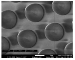
図7~9は、サファイア加工基板上に形成した突起を示す。
突起の最大外径は2.1μm、高さは1.1μm、及び側面のサファイア基板の主面に対する傾斜角度は59°であった。正三角形格子における正三角形の一辺の長さは3.0μmであった。従って、相互に隣接する一対の突起間の間隔は0.9μmであった。加工基板の基板表面の平面視における突起を排除した主面部分の専有面積率は54.7%であった。
また、角度θが30°及び45°のサファイア加工基板を作製した。さらに、参考として、角度θが0°(60°)のサファイア加工基板も作製した。
(試験評価方法)
角度θが0°、15°、30°及び45°のそれぞれのサファイア加工基板について、基板上にGaNを結晶成長させ、その表面における暗点密度を、カソードルミネッセンス(CL)法によって測定した。
角度θが0°、15°、30°及び45°のそれぞれのサファイア加工基板について、基板上にGaNを結晶成長させ、その表面における暗点密度を、カソードルミネッセンス(CL)法によって測定した。
(試験評価結果)
図10は、角度θとサファイア加工基板上に形成したGaN層の表面の暗点密度との関係を示す。
図10は、角度θとサファイア加工基板上に形成したGaN層の表面の暗点密度との関係を示す。
角度θが0°(60°)のサファイア加工基板では、暗点密度が1.19×10⁸個/cm2であった。角度θが15°のサファイア加工基板では、暗点密度が9.90×107個/cm2であった。角度θが30°のサファイア加工基板では、暗点密度が9.69×107個/cm2であった。角度θが45°のサファイア加工基板では、暗点密度が1.10×108個/cm2であった。
図10によれば、角度θが0°よりも大きく且つ60°よりも小さいと、GaN層の表面の暗点密度が小さくなることが分かる。暗点密度を低減する観点からは、角度θが10~40°であることが好ましく、15~35°であることがより好ましく、25~35°がさらに好ましく、30°であることが最も好ましい。
本発明は、加工基板及びそれを用いた半導体装置について有用である。
W ウエハ
R フォトレジスト
10 半導体発光素子
11 加工基板
11’ ウエハ加工基板
12 突起
13 u-GaN層
14 n型GaN層
15 多重量子井戸層
15a 井戸層
15b 障壁層
16 p型GaN層
17 n型電極
18 p型電極
R フォトレジスト
10 半導体発光素子
11 加工基板
11’ ウエハ加工基板
12 突起
13 u-GaN層
14 n型GaN層
15 多重量子井戸層
15a 井戸層
15b 障壁層
16 p型GaN層
17 n型電極
18 p型電極
Claims (15)
- 基板表面に、平面視において正三角形格子を構成するように配設された複数の突起が形成され、基板上に主面がc面のGaNが結晶成長し得る加工基板であって、
前記複数の突起は、前記複数の突起によって構成される正三角形格子における正三角形の3本の辺が、基板上に主面がc面のGaNが結晶成長したときにおけるGaNのa軸に対して反時計回りになす角度のうち、最も小さい角度が10~50°となるように配設されている加工基板。 - 請求項1に記載された加工基板において、
前記複数の突起によって構成される正三角形格子における正三角形の3本の辺が、基板上に主面がc面のGaNが結晶成長したときにおけるGaNのa軸に対して反時計回りになす角度のうち、最も小さい角度が10~40°である加工基板。 - 請求項2に記載された加工基板において、
前記複数の突起によって構成される正三角形格子における正三角形の3本の辺が、基板上に主面がc面のGaNが結晶成長したときにおけるGaNのa軸に対して反時計回りになす角度のうち、最も小さい角度が25~35°である加工基板。 - 請求項1乃至3のいずれかに記載された加工基板において、
前記突起の形状が円錐又は円錐台である加工基板。 - 請求項1乃至4のいずれかに記載された加工基板において、
前記突起の最大外径が1μm以上である加工基板。 - 請求項1乃至5のいずれかに記載された加工基板において、
前記突起の高さが0.5μm以上である加工基板。 - 請求項1乃至6のいずれかに記載された加工基板において、
前記突起は、その最大外径が高さよりも大きい加工基板。 - 請求項1乃至7のいずれかに記載された加工基板において、
前記正三角形格子における正三角形の一辺の長さが2μm以上である加工基板。 - 請求項1乃至8のいずれかに記載された加工基板において、
前記正三角形格子における正三角形の一辺の長さが前記突起の最大外径よりも大きい加工基板。 - 請求項1乃至9のいずれかに記載された加工基板において、
前記正三角形格子における同じ正三角形に含まれる2個の頂点の一対の突起が相互に間隔を有して配設されている加工基板。 - 請求項10に記載された加工基板において、
前記正三角形格子における同じ正三角形に含まれる2個の頂点の一対の突起の間隔が0.1~2.0μmである加工基板。 - 請求項1乃至11のいずれかに記載された加工基板において、
前記加工基板が、サファイア加工基板、Si加工基板、又はSiC加工基板である加工基板。 - 請求項12に記載された加工基板において、
前記加工基板が、主面がc面のサファイア加工基板であり、
前記複数の突起は、前記複数の突起によって構成される正三角形格子における正三角形の3本の辺がサファイアのm軸に対して反時計回りになす角度のうち、最も小さい角度が10~50°となるように配設されている加工基板。 - 基板表面に、平面視において正三角形格子を構成するように配設された複数の突起が形成された加工基板と、
前記加工基板上に主面がc面のGaNが結晶成長して形成されたGaN層と、
を備えた半導体装置であって、
前記加工基板の前記複数の突起は、前記複数の突起によって構成される正三角形格子における正三角形の3本の辺が、前記GaN層を構成するGaNのa軸に対して反時計回りになす角度のうち、最も小さい角度が10~50°となるように配設されている半導体装置。 - 請求項14に記載された半導体装置において、
前記GaN層の表面におけるカソードルミネッセンス法によって測定される暗点密度が1.15×10⁸個/cm2以下である半導体装置。
Priority Applications (1)
| Application Number | Priority Date | Filing Date | Title |
|---|---|---|---|
| JP2015504152A JPWO2014136393A1 (ja) | 2013-03-08 | 2014-02-21 | 加工基板及びそれを用いた半導体装置 |
Applications Claiming Priority (2)
| Application Number | Priority Date | Filing Date | Title |
|---|---|---|---|
| JP2013047176 | 2013-03-08 | ||
| JP2013-047176 | 2013-03-08 |
Publications (1)
| Publication Number | Publication Date |
|---|---|
| WO2014136393A1 true WO2014136393A1 (ja) | 2014-09-12 |
Family
ID=51490932
Family Applications (1)
| Application Number | Title | Priority Date | Filing Date |
|---|---|---|---|
| PCT/JP2014/000897 Ceased WO2014136393A1 (ja) | 2013-03-08 | 2014-02-21 | 加工基板及びそれを用いた半導体装置 |
Country Status (2)
| Country | Link |
|---|---|
| JP (1) | JPWO2014136393A1 (ja) |
| WO (1) | WO2014136393A1 (ja) |
Cited By (4)
| Publication number | Priority date | Publication date | Assignee | Title |
|---|---|---|---|---|
| WO2016042890A1 (ja) * | 2014-09-17 | 2016-03-24 | 住友化学株式会社 | 窒化物半導体テンプレートの製造方法 |
| EP3007237A4 (en) * | 2013-05-31 | 2016-04-27 | Asahi Kasei E Materials Corp | LED PATTERN WAFER, EPITAKTIC WAFER WITH LEDS, AND METHOD OF PRODUCTION OF THE EPITACTIC WAFER WITH LEDS |
| WO2017134708A1 (ja) * | 2016-02-01 | 2017-08-10 | パナソニック株式会社 | エピタキシャル基板 |
| JP2018032745A (ja) * | 2016-08-24 | 2018-03-01 | 東芝メモリ株式会社 | ドレッサー、ドレッサーの製造方法、及び半導体装置の製造方法 |
Citations (5)
| Publication number | Priority date | Publication date | Assignee | Title |
|---|---|---|---|---|
| WO2012093601A1 (ja) * | 2011-01-07 | 2012-07-12 | 三菱化学株式会社 | エピタキシャル成長用基板およびGaN系LEDデバイス |
| JP2012160502A (ja) * | 2011-01-31 | 2012-08-23 | Nichia Chem Ind Ltd | 半導体発光素子用基板およびその製造方法、並びにその基板を用いた半導体発光素子 |
| JP2012184144A (ja) * | 2011-03-07 | 2012-09-27 | Tokuyama Corp | 窒化ガリウム結晶積層基板及びその製造方法 |
| JP2012197194A (ja) * | 2011-03-18 | 2012-10-18 | Ricoh Co Ltd | 13族窒化物結晶の製造方法、13族窒化物結晶基板の製造方法、13族窒化物結晶および13族窒化物結晶基板 |
| JP2013173641A (ja) * | 2012-02-24 | 2013-09-05 | Tokuyama Corp | 窒化ガリウム結晶積層基板及びその製造方法 |
-
2014
- 2014-02-21 WO PCT/JP2014/000897 patent/WO2014136393A1/ja not_active Ceased
- 2014-02-21 JP JP2015504152A patent/JPWO2014136393A1/ja active Pending
Patent Citations (5)
| Publication number | Priority date | Publication date | Assignee | Title |
|---|---|---|---|---|
| WO2012093601A1 (ja) * | 2011-01-07 | 2012-07-12 | 三菱化学株式会社 | エピタキシャル成長用基板およびGaN系LEDデバイス |
| JP2012160502A (ja) * | 2011-01-31 | 2012-08-23 | Nichia Chem Ind Ltd | 半導体発光素子用基板およびその製造方法、並びにその基板を用いた半導体発光素子 |
| JP2012184144A (ja) * | 2011-03-07 | 2012-09-27 | Tokuyama Corp | 窒化ガリウム結晶積層基板及びその製造方法 |
| JP2012197194A (ja) * | 2011-03-18 | 2012-10-18 | Ricoh Co Ltd | 13族窒化物結晶の製造方法、13族窒化物結晶基板の製造方法、13族窒化物結晶および13族窒化物結晶基板 |
| JP2013173641A (ja) * | 2012-02-24 | 2013-09-05 | Tokuyama Corp | 窒化ガリウム結晶積層基板及びその製造方法 |
Cited By (10)
| Publication number | Priority date | Publication date | Assignee | Title |
|---|---|---|---|---|
| EP3007237A4 (en) * | 2013-05-31 | 2016-04-27 | Asahi Kasei E Materials Corp | LED PATTERN WAFER, EPITAKTIC WAFER WITH LEDS, AND METHOD OF PRODUCTION OF THE EPITACTIC WAFER WITH LEDS |
| US9660141B2 (en) | 2013-05-31 | 2017-05-23 | Asahi Kasei E-Materials Corporation | Pattern wafer for LEDs, epitaxial wafer for LEDs and method of manufacturing the epitaxial wafer for LEDs |
| WO2016042890A1 (ja) * | 2014-09-17 | 2016-03-24 | 住友化学株式会社 | 窒化物半導体テンプレートの製造方法 |
| JP2016063022A (ja) * | 2014-09-17 | 2016-04-25 | 住友化学株式会社 | 窒化物半導体テンプレートの製造方法 |
| CN107078033A (zh) * | 2014-09-17 | 2017-08-18 | 住友化学株式会社 | 氮化物半导体模板的制造方法 |
| US10062807B2 (en) | 2014-09-17 | 2018-08-28 | Sumitomo Chemical Company, Limited | Method for manufacturing nitride semiconductor template |
| CN107078033B (zh) * | 2014-09-17 | 2020-11-10 | 住友化学株式会社 | 氮化物半导体模板的制造方法 |
| WO2017134708A1 (ja) * | 2016-02-01 | 2017-08-10 | パナソニック株式会社 | エピタキシャル基板 |
| US10697089B2 (en) | 2016-02-01 | 2020-06-30 | Panasonic Corporation | Epitaxial substrate |
| JP2018032745A (ja) * | 2016-08-24 | 2018-03-01 | 東芝メモリ株式会社 | ドレッサー、ドレッサーの製造方法、及び半導体装置の製造方法 |
Also Published As
| Publication number | Publication date |
|---|---|
| JPWO2014136393A1 (ja) | 2017-02-09 |
Similar Documents
| Publication | Publication Date | Title |
|---|---|---|
| US8735867B2 (en) | Group III nitride nanorod light emitting device | |
| US8946772B2 (en) | Substrate for epitaxial growth, process for manufacturing GaN-based semiconductor film, GaN-based semiconductor film, process for manufacturing GaN-based semiconductor light emitting element and GaN-based semiconductor light emitting element | |
| JP5854419B2 (ja) | 多波長発光素子及びその製造方法 | |
| CN102576780B (zh) | 不平坦图案化的基底上的高质量非极性/半极性半导体器件及其制造方法 | |
| KR20100093872A (ko) | 질화물 반도체 발광소자 및 그 제조방법 | |
| JP6686172B2 (ja) | 窒化物半導体発光素子 | |
| JP6019541B2 (ja) | 半導体発光素子 | |
| WO2014136393A1 (ja) | 加工基板及びそれを用いた半導体装置 | |
| US9812607B2 (en) | Method for manufacturing nitride semiconductor template | |
| JP5822190B2 (ja) | 多波長発光素子及びその製造方法 | |
| JP5557180B2 (ja) | 半導体発光素子の製造方法 | |
| JP3696003B2 (ja) | 窒化物系半導体層の形成方法 | |
| US10062807B2 (en) | Method for manufacturing nitride semiconductor template | |
| JP2009123836A (ja) | 窒化物半導体発光素子 | |
| JP6124740B2 (ja) | 窒化物半導体発光素子の製造方法、窒化物半導体発光素子および窒化物半導体発光素子用下地基板 | |
| JP4924498B2 (ja) | 窒化物系半導体発光素子、エピタキシャルウエハ、及び窒化物系半導体発光素子を作製する方法 | |
| JP2009141085A (ja) | 窒化物半導体素子 | |
| JP2007036174A (ja) | 窒化ガリウム系発光ダイオード | |
| TWI545798B (zh) | Nitride semiconductor light emitting device and manufacturing method thereof | |
| JP7305428B2 (ja) | 半導体成長用基板、半導体素子、半導体発光素子および半導体素子製造方法 | |
| JP5190343B2 (ja) | 半導体素子の製造方法 | |
| JP2008227103A (ja) | GaN系半導体発光素子 | |
| JP2005020026A (ja) | 窒化ガリウム系化合物半導体及び半導体基板 | |
| JP2005020027A (ja) | 窒化ガリウム系化合物半導体の製造方法 | |
| JP5376462B2 (ja) | 半導体発光素子及びその製造方法 |
Legal Events
| Date | Code | Title | Description |
|---|---|---|---|
| 121 | Ep: the epo has been informed by wipo that ep was designated in this application |
Ref document number: 14760268 Country of ref document: EP Kind code of ref document: A1 |
|
| ENP | Entry into the national phase |
Ref document number: 2015504152 Country of ref document: JP Kind code of ref document: A |
|
| NENP | Non-entry into the national phase |
Ref country code: DE |
|
| 122 | Ep: pct application non-entry in european phase |
Ref document number: 14760268 Country of ref document: EP Kind code of ref document: A1 |