WO2014129191A1 - 液晶装置、液晶装置の製造方法、及び電子機器 - Google Patents
液晶装置、液晶装置の製造方法、及び電子機器 Download PDFInfo
- Publication number
- WO2014129191A1 WO2014129191A1 PCT/JP2014/000880 JP2014000880W WO2014129191A1 WO 2014129191 A1 WO2014129191 A1 WO 2014129191A1 JP 2014000880 W JP2014000880 W JP 2014000880W WO 2014129191 A1 WO2014129191 A1 WO 2014129191A1
- Authority
- WO
- WIPO (PCT)
- Prior art keywords
- liquid crystal
- sealing material
- substrate
- alignment film
- crystal device
- Prior art date
- Legal status (The legal status is an assumption and is not a legal conclusion. Google has not performed a legal analysis and makes no representation as to the accuracy of the status listed.)
- Ceased
Links
Images





Classifications
-
- G—PHYSICS
- G02—OPTICS
- G02F—OPTICAL DEVICES OR ARRANGEMENTS FOR THE CONTROL OF LIGHT BY MODIFICATION OF THE OPTICAL PROPERTIES OF THE MEDIA OF THE ELEMENTS INVOLVED THEREIN; NON-LINEAR OPTICS; FREQUENCY-CHANGING OF LIGHT; OPTICAL LOGIC ELEMENTS; OPTICAL ANALOGUE/DIGITAL CONVERTERS
- G02F1/00—Devices or arrangements for the control of the intensity, colour, phase, polarisation or direction of light arriving from an independent light source, e.g. switching, gating or modulating; Non-linear optics
- G02F1/01—Devices or arrangements for the control of the intensity, colour, phase, polarisation or direction of light arriving from an independent light source, e.g. switching, gating or modulating; Non-linear optics for the control of the intensity, phase, polarisation or colour
- G02F1/13—Devices or arrangements for the control of the intensity, colour, phase, polarisation or direction of light arriving from an independent light source, e.g. switching, gating or modulating; Non-linear optics for the control of the intensity, phase, polarisation or colour based on liquid crystals, e.g. single liquid crystal display cells
- G02F1/133—Constructional arrangements; Operation of liquid crystal cells; Circuit arrangements
- G02F1/1333—Constructional arrangements; Manufacturing methods
- G02F1/1339—Gaskets; Spacers; Sealing of cells
-
- G—PHYSICS
- G02—OPTICS
- G02F—OPTICAL DEVICES OR ARRANGEMENTS FOR THE CONTROL OF LIGHT BY MODIFICATION OF THE OPTICAL PROPERTIES OF THE MEDIA OF THE ELEMENTS INVOLVED THEREIN; NON-LINEAR OPTICS; FREQUENCY-CHANGING OF LIGHT; OPTICAL LOGIC ELEMENTS; OPTICAL ANALOGUE/DIGITAL CONVERTERS
- G02F1/00—Devices or arrangements for the control of the intensity, colour, phase, polarisation or direction of light arriving from an independent light source, e.g. switching, gating or modulating; Non-linear optics
- G02F1/01—Devices or arrangements for the control of the intensity, colour, phase, polarisation or direction of light arriving from an independent light source, e.g. switching, gating or modulating; Non-linear optics for the control of the intensity, phase, polarisation or colour
- G02F1/13—Devices or arrangements for the control of the intensity, colour, phase, polarisation or direction of light arriving from an independent light source, e.g. switching, gating or modulating; Non-linear optics for the control of the intensity, phase, polarisation or colour based on liquid crystals, e.g. single liquid crystal display cells
- G02F1/133—Constructional arrangements; Operation of liquid crystal cells; Circuit arrangements
- G02F1/1333—Constructional arrangements; Manufacturing methods
- G02F1/1337—Surface-induced orientation of the liquid crystal molecules, e.g. by alignment layers
- G02F1/133734—Surface-induced orientation of the liquid crystal molecules, e.g. by alignment layers by obliquely evaporated films, e.g. Si or SiO2 films
-
- G—PHYSICS
- G02—OPTICS
- G02F—OPTICAL DEVICES OR ARRANGEMENTS FOR THE CONTROL OF LIGHT BY MODIFICATION OF THE OPTICAL PROPERTIES OF THE MEDIA OF THE ELEMENTS INVOLVED THEREIN; NON-LINEAR OPTICS; FREQUENCY-CHANGING OF LIGHT; OPTICAL LOGIC ELEMENTS; OPTICAL ANALOGUE/DIGITAL CONVERTERS
- G02F1/00—Devices or arrangements for the control of the intensity, colour, phase, polarisation or direction of light arriving from an independent light source, e.g. switching, gating or modulating; Non-linear optics
- G02F1/01—Devices or arrangements for the control of the intensity, colour, phase, polarisation or direction of light arriving from an independent light source, e.g. switching, gating or modulating; Non-linear optics for the control of the intensity, phase, polarisation or colour
- G02F1/13—Devices or arrangements for the control of the intensity, colour, phase, polarisation or direction of light arriving from an independent light source, e.g. switching, gating or modulating; Non-linear optics for the control of the intensity, phase, polarisation or colour based on liquid crystals, e.g. single liquid crystal display cells
- G02F1/133—Constructional arrangements; Operation of liquid crystal cells; Circuit arrangements
- G02F1/1333—Constructional arrangements; Manufacturing methods
- G02F1/1341—Filling or closing of cells
-
- G—PHYSICS
- G02—OPTICS
- G02F—OPTICAL DEVICES OR ARRANGEMENTS FOR THE CONTROL OF LIGHT BY MODIFICATION OF THE OPTICAL PROPERTIES OF THE MEDIA OF THE ELEMENTS INVOLVED THEREIN; NON-LINEAR OPTICS; FREQUENCY-CHANGING OF LIGHT; OPTICAL LOGIC ELEMENTS; OPTICAL ANALOGUE/DIGITAL CONVERTERS
- G02F1/00—Devices or arrangements for the control of the intensity, colour, phase, polarisation or direction of light arriving from an independent light source, e.g. switching, gating or modulating; Non-linear optics
- G02F1/01—Devices or arrangements for the control of the intensity, colour, phase, polarisation or direction of light arriving from an independent light source, e.g. switching, gating or modulating; Non-linear optics for the control of the intensity, phase, polarisation or colour
- G02F1/13—Devices or arrangements for the control of the intensity, colour, phase, polarisation or direction of light arriving from an independent light source, e.g. switching, gating or modulating; Non-linear optics for the control of the intensity, phase, polarisation or colour based on liquid crystals, e.g. single liquid crystal display cells
- G02F1/133—Constructional arrangements; Operation of liquid crystal cells; Circuit arrangements
- G02F1/1333—Constructional arrangements; Manufacturing methods
- G02F1/1337—Surface-induced orientation of the liquid crystal molecules, e.g. by alignment layers
- G02F1/133742—Surface-induced orientation of the liquid crystal molecules, e.g. by alignment layers for homeotropic alignment
Definitions
- the present invention relates to a liquid crystal device, a method for manufacturing the liquid crystal device, and an electronic apparatus.
- liquid crystal devices for example, an active drive type liquid crystal device including a transistor for each pixel as an element for switching control of a pixel electrode is known.
- Liquid crystal devices are used in, for example, direct-view displays and projector light valves.
- an inorganic alignment film is formed on a substrate from an effective display region in a plan view to a region between the effective display region and the sealing material.
- a sealing material is formed so as to surround the effective display area on the substrate.
- a pair of substrates are bonded together, and liquid crystal is injected into the region surrounded by the sealing material through the injection port. After the injection, the injection port is sealed with a sealing material.
- an inorganic alignment film is formed in a region inside the sealing material, and the contact surface between the sealing material and the sealing material and the substrate is relatively flat. There is a problem that may be peeled off.
- the aspect of the present invention has been made to solve at least a part of the above problems, and can be realized as the following forms or application examples.
- a liquid crystal device includes a first substrate, a second substrate disposed opposite to the first substrate, and a seal disposed between the first substrate and the second substrate.
- a material a liquid crystal layer disposed between the first substrate and the second substrate, a sealing material for sealing the liquid crystal layer in an opening region of the sealing material, the first substrate and the liquid crystal layer And a second inorganic alignment film disposed between the second substrate and the liquid crystal layer, wherein the first inorganic alignment film includes the second inorganic alignment film.
- the sealing material is disposed in a region overlapping with at least a part of the region in which the sealing material is disposed.
- the first inorganic alignment film is extended and provided under the sealing material (a region overlapping in plan view), so that the columnar structures (columns) constituting the first inorganic alignment film Following the unevenness, the first substrate can be made uneven. Therefore, when the sealing material is provided in the opening region on the first substrate, the contact area with the sealing material can be increased by the unevenness on the first substrate, and the sealing material is prevented from peeling off from the first substrate. be able to.
- the first inorganic alignment film is disposed so as to include a region where the sealing material is disposed when viewed from the second substrate side. Preferably it is.
- the first inorganic alignment film is provided under the sealing material, on the first substrate following the unevenness of the columnar structure (column) constituting the first inorganic alignment film. It becomes possible to make it uneven. Therefore, when the sealing material is provided in the opening region on the first substrate, the contact area with the sealing material can be increased from the first application example due to the unevenness on the first substrate. Can be prevented from peeling off.
- the first inorganic alignment film is disposed so as to overlap at least a part of a region where the sealing material is disposed when viewed from the second substrate side. It is preferable that
- the unevenness on the first substrate follows the unevenness of the columnar structure (column) constituting the first inorganic alignment film. It becomes possible to. Therefore, when the sealing material is provided in the sealing material forming region on the first substrate, the contact area with the sealing material can be increased due to the unevenness on the first substrate, and the sealing material is prevented from peeling off from the first substrate. Can do.
- a surface layer is disposed between the first inorganic alignment film and the sealing material.
- the surface layer since the surface layer is provided between the sealing material and the first inorganic alignment film, the surface layer surface follows the unevenness of the columnar structure constituting the first inorganic alignment film. Can be made uneven. Therefore, when the sealing material is provided in the opening region on the surface layer, the contact area with the sealing material can be increased by the unevenness of the surface of the surface layer, and the sealing material can be prevented from peeling off from the surface layer. it can. In addition, since the surface layer is provided, light resistance can be improved, and the liquid crystal device can be irradiated with strong light.
- an inorganic alignment film forming step of forming a first inorganic alignment film on a first substrate, and a sealing material is formed on the first substrate. From the sealing material forming step, the bonding step of bonding the first substrate and the second substrate on which the second inorganic alignment film is formed via the sealing material, and the first region from the opening region of the sealing material.
- the first inorganic alignment film is formed under the sealing material, the first substrate is made uneven according to the unevenness of the columnar structure (column) constituting the first inorganic alignment film. It becomes possible to do. Therefore, when the sealing material is formed in the opening region on the first substrate, the contact area with the sealing material can be increased due to the unevenness on the first substrate, and the sealing material is prevented from peeling off from the first substrate. be able to.
- Application Example 6 In the method for manufacturing a liquid crystal device according to the application example described above, it is preferable to include a surface treatment process for performing a surface treatment on the surface of the first inorganic alignment film.
- the surface treatment is performed on the first inorganic alignment film, the surface of the surface layer subjected to the surface treatment is made uneven according to the unevenness of the columnar structure constituting the first inorganic alignment film. It becomes possible. Therefore, when the sealing material is provided in the opening region on the surface layer, the contact area with the sealing material can be increased by the unevenness of the surface of the surface layer, and the sealing material can be prevented from peeling off from the surface layer. it can. In addition, since the surface layer is provided, light resistance can be improved, and the liquid crystal device can be irradiated with strong light.
- An electronic apparatus includes the liquid crystal device described above.
- FIG. 2 is a schematic plan view illustrating a configuration of a liquid crystal device.
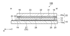
- FIG. 2 is a schematic cross-sectional view taken along the line H-H ′ of the liquid crystal device illustrated in FIG. 1.
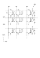
- FIG. 3 is an equivalent circuit diagram illustrating an electrical configuration of the liquid crystal device.
- FIG. 3 is a schematic cross-sectional view illustrating a structure of a liquid crystal device. The schematic top view which mainly shows the structure of an inorganic alignment film and a sealing material (sealing material) among liquid crystal devices.
- FIG. 6 is a schematic cross-sectional view taken along the line A-A ′ of the liquid crystal device shown in FIG. 5.
- 5 is a flowchart showing a method for manufacturing a liquid crystal device in the order of steps.
- FIG. 6 is a schematic plan view illustrating a configuration of a liquid crystal device according to a modification.
- the substrate when “on the substrate” is described, the substrate is disposed so as to be in contact with the substrate, or is disposed on the substrate via another component, or the substrate. It is assumed that a part is arranged so as to be in contact with each other and a part is arranged via another component.
- an active matrix liquid crystal device including a thin film transistor (TFT) as a pixel switching element will be described as an example of the liquid crystal device.
- TFT thin film transistor
- This liquid crystal device can be suitably used, for example, as a light modulation element (liquid crystal light valve) of a projection display device (liquid crystal projector).
- FIG. 1 is a schematic plan view showing the configuration of the liquid crystal device.
- FIG. 2 is a schematic cross-sectional view taken along the line HH ′ of the liquid crystal device shown in FIG.
- FIG. 3 is an equivalent circuit diagram showing an electrical configuration of the liquid crystal device.
- the configuration of the liquid crystal device will be described with reference to FIGS.
- the liquid crystal device 100 As shown in FIGS. 1 and 2, the liquid crystal device 100 according to the present embodiment is sandwiched between the element substrate 10 (first substrate) and the counter substrate 20 (second substrate) arranged opposite to each other and the pair of substrates. And a liquid crystal layer 15.
- a transparent substrate such as a glass substrate or a quartz substrate is used.
- the element substrate 10 is larger than the counter substrate 20, and both the substrates are bonded via a sealing material 14 disposed along the outer periphery of the counter substrate 20.
- a sealing material 14 disposed along the outer periphery of the counter substrate 20.
- liquid crystal having positive or negative dielectric anisotropy is sealed between the opposing substrates 20 inside the sealing material 14 provided in an annular shape in plan view, thereby forming a liquid crystal layer 15.
- an adhesive such as a thermosetting or ultraviolet curable epoxy resin is employed.
- Spacers are mixed in the sealing material 14 to keep the distance between the pair of substrates constant.
- a display area E in which a plurality of pixels P are arranged is provided inside the inner edge of the seal material 14.
- the display area E may include dummy pixels arranged so as to surround the plurality of pixels P in addition to the plurality of pixels P contributing to display.
- a light shielding film black matrix; BM
- BM black matrix
- a data line driving circuit 22 is provided between the sealing material 14 along one side of the element substrate 10 and the one side. Further, an inspection circuit 25 is provided between the sealing material 14 and the display area E along the other one side facing the one side. Further, a scanning line driving circuit 24 is provided between the sealing material 14 and the display area E along the other two sides that are orthogonal to the one side and face each other. A plurality of wirings 29 connecting the two scanning line driving circuits 24 are provided between the sealing material 14 and the inspection circuit 25 along the other one side facing the one side.
- a light shielding film 18 (parting portion) is provided between the sealing material 14 arranged in a ring shape on the counter substrate 20 and the display area E.
- the light shielding film 18 is made of, for example, a light shielding metal or metal oxide, and the inside of the light shielding film 18 is a display area E having a plurality of pixels P.
- a light shielding film that divides a plurality of pixels P in a plane is also provided in the display area E.
- the wirings connected to the data line driving circuit 22 and the scanning line driving circuit 24 are connected to a plurality of external connection terminals 61 arranged along the one side.
- the direction along the one side will be referred to as the X direction
- the direction along the other two sides orthogonal to the one side and facing each other will be described as the Y direction.
- TFT 30 Thin Film Transistor, TFT
- the element substrate 10 in the present invention includes at least the pixel electrode 27, the TFT 30, and the first inorganic alignment film 28.
- the counter substrate 20 in the present invention includes at least the counter electrode 31 and the second inorganic alignment film 32.
- the light shielding film 18 surrounds the display area E and is provided at a position overlapping the scanning line driving circuit 24 and the inspection circuit 25 in plan view.
- the light incident on the peripheral circuit including these drive circuits from the counter substrate 20 side is shielded, and the peripheral circuit is prevented from malfunctioning due to the light. Further, unnecessary stray light is shielded from entering the display area E, and high contrast in the display of the display area E is ensured.
- the planarization layer 33 is made of an inorganic material such as silicon oxide, for example, and is provided so as to cover the light shielding film 18 with light transmittance.
- a method for forming such a planarizing layer 33 for example, a method of forming a film by using a plasma CVD (Chemical Vapor Deposition) method or the like can be cited.
- the counter electrode 31 is made of a transparent conductive film such as ITO (Indium Tin Oxide), for example, and covers the planarization layer 33, and as shown in FIG. 1, the element substrate is formed by the vertical conduction portions 26 provided at the four corners of the counter substrate 20. It is electrically connected to the wiring on the 10 side.
- ITO Indium Tin Oxide
- the first inorganic alignment film 28 covering the pixel electrode 27 and the second inorganic alignment film 32 covering the counter electrode 31 are selected based on the optical design of the liquid crystal device 100.
- an inorganic alignment film formed by depositing an inorganic material such as SiOx (silicon oxide) using a vapor deposition method and substantially vertically aligning with liquid crystal molecules having negative dielectric anisotropy can be given.
- Such a liquid crystal device 100 is of a transmissive type, and the transmittance of the pixel P when no voltage is applied is larger than the transmittance when the voltage is applied, resulting in a normally white display, or when no voltage is applied.
- a normally black mode optical design is adopted in which the transmittance of the pixel P is smaller than the transmittance when a voltage is applied and dark display is achieved.
- Polarizing elements are arranged and used according to the optical design on the light incident side and the light exit side, respectively.
- the liquid crystal device 100 includes a plurality of scanning lines 3a and a plurality of data lines 6a that are insulated from each other and orthogonal to each other in at least the display region E, and capacitance lines 3b.
- the direction in which the scanning line 3a extends is the X direction
- the direction in which the data line 6a extends is the Y direction.
- the scanning line 3a, the data line 6a, the capacitor line 3b, the pixel electrode 27, the TFT 30, and the capacitor element 16 are provided, and these constitute the pixel circuit of the pixel P.
- the scanning line 3a is electrically connected to the gate of the TFT 30, and the data line 6a is electrically connected to the data line side source / drain region (source region) of the TFT 30.
- the pixel electrode 27 is electrically connected to the pixel electrode side source / drain region (drain region) of the TFT 30.
- the data line 6a is connected to the data line driving circuit 22 (see FIG. 1), and supplies image signals D1, D2,..., Dn supplied from the data line driving circuit 22 to the pixels P.
- the scanning line 3a is connected to the scanning line driving circuit 24 (see FIG. 1), and supplies the scanning signals SC1, SC2,..., SCm supplied from the scanning line driving circuit 24 to each pixel P.
- the image signals D1 to Dn supplied from the data line driving circuit 22 to the data lines 6a may be supplied line-sequentially in this order, or may be supplied to a plurality of adjacent data lines 6a for each group. Good.
- the scanning line driving circuit 24 supplies the scanning signals SC1 to SCm to the scanning line 3a at a predetermined timing.
- the TFT 30 as a switching element is turned on for a certain period by the input of the scanning signals SC1 to SCm, so that the image signals D1 to Dn supplied from the data line 6a are supplied to the pixel electrode 27 at a predetermined timing. It is the structure written in. A predetermined level of the image signals D1 to Dn written to the liquid crystal layer 15 through the pixel electrode 27 is held for a certain period between the pixel electrode 27 and the counter electrode 31 disposed to face the liquid crystal layer 15.
- the capacitive element 16 is connected in parallel with the liquid crystal capacitance formed between the pixel electrode 27 and the counter electrode 31.
- the capacitive element 16 is provided between the pixel electrode side source / drain region of the TFT 30 and the capacitive line 3b.
- the capacitive element 16 has a dielectric layer between two capacitive electrodes.
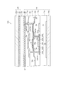
- FIG. 4 is a schematic cross-sectional view showing the structure of the liquid crystal device.
- the structure of the liquid crystal device will be described with reference to FIG.
- FIG. 4 shows the cross-sectional positional relationship of each component and is expressed on a scale that can be clearly shown.
- the liquid crystal device 100 includes an element substrate 10 that is one of a pair of substrates, and a counter substrate 20 that is the other substrate disposed opposite thereto.
- the first base material 10a configuring the element substrate 10 and the second base material 20a configuring the counter substrate 20 are configured by, for example, a quartz substrate or the like.
- a lower light-shielding film 3c made of titanium (Ti), chromium (Cr), or the like is formed on the first base material 10a.
- the lower light-shielding film 3c is planarly patterned in a lattice shape and defines an opening area of each pixel.
- the lower light shielding film 3c may function as a part of the scanning line 3a.
- a base insulating layer 11a made of a silicon oxide film or the like is formed on the first base material 10a and the lower light shielding film 3c.
- the TFT 30 and the scanning line 3a are formed on the base insulating layer 11a.
- the TFT 30 has, for example, an LDD (Lightly Doped Drain) structure, and is formed on the semiconductor layer 30a made of polysilicon or the like, the gate insulating film 11g formed on the semiconductor layer 30a, and the gate insulating film 11g. And a gate electrode 30g made of a polysilicon film or the like.
- the scanning line 3a also functions as the gate electrode 30g.
- the semiconductor layer 30a is formed as an N-type TFT 30 by implanting N-type impurity ions such as phosphorus (P) ions.
- the semiconductor layer 30a includes a channel region 30c, a data line side LDD region 30s1, a data line side source / drain region 30s, a pixel electrode side LDD region 30d1, and a pixel electrode side source / drain region 30d. ing.
- the channel region 30c is doped with P-type impurity ions such as boron (B) ions.
- the other regions (30s1, 30s, 30d1, 30d) are doped with N-type impurity ions such as phosphorus (P) ions.
- the TFT 30 is formed as an N-type TFT.
- a first interlayer insulating layer 11b made of a silicon oxide film or the like is formed on the gate electrode 30g, the base insulating layer 11a, and the scanning line 3a.
- a capacitive element 16 is provided on the first interlayer insulating layer 11b.
- the first capacitor electrode 16a as the pixel potential side capacitor electrode electrically connected to the pixel electrode side source / drain region 30d and the pixel electrode 27 of the TFT 30, and the capacitor line 3b (as the fixed potential side capacitor electrode).
- a part of the second capacitor electrode 16b) is disposed to face the dielectric film 16c, whereby the capacitor element 16 is formed.
- the capacitor line 3b includes at least one of refractory metals such as Ti (titanium), Cr (chromium), W (tungsten), Ta (tantalum), and Mo (molybdenum). , Metal simple substance, alloy, metal silicide, polysilicide, and a laminate of these. Alternatively, it can be formed from an Al (aluminum) film.
- the first capacitor electrode 16a is made of, for example, a conductive polysilicon film and functions as a pixel potential side capacitor electrode of the capacitor element 16.
- the first capacitor electrode 16a may be composed of a single layer film or a multilayer film containing a metal or an alloy, like the capacitor line 3b.
- the first capacitor electrode 16a functions as a pixel potential side capacitor electrode, and in addition to the pixel electrode 27 and the pixel electrode side source / drain region 30d (drain) via the contact hole CNT52, the relay layer 55, and the contact holes CNT53 and CNT51. A region).
- the data line 6a is formed on the capacitive element 16 via the second interlayer insulating layer 11c.
- the data line 6a is electrically connected to the data line side source / drain region 30s (source region) of the semiconductor layer 30a through the contact hole CNT54 formed in the first interlayer insulating layer 11b and the second interlayer insulating layer 11c. Has been.
- a pixel electrode 27 is formed on the data line 6a via a third interlayer insulating layer 11d.
- the pixel electrode 27 is connected to the first capacitor electrode 16a via the contact holes CNT52, CNT53, and the relay layer 55 that are opened in the second interlayer insulating layer 11c and the third interlayer insulating layer 11d, whereby the semiconductor layer 30a.
- the pixel electrode side source / drain region 30d (drain region) is electrically connected.
- the pixel electrode 27 is formed of a transparent conductive film such as an ITO film, for example.
- a first inorganic alignment film 28 obtained by obliquely depositing an inorganic material such as silicon oxide (SiO 2 ) is provided.
- an inorganic material such as silicon oxide (SiO 2 )
- a liquid crystal layer 15 in which liquid crystal or the like is sealed in a space surrounded by the sealing material 14 is provided.
- the counter electrode 31 is provided on the entire surface of the second base material 20a.
- a second inorganic alignment film 32 is provided by obliquely depositing an inorganic material such as silicon oxide (SiO 2 ).
- the counter electrode 31 is made of a transparent conductive film such as an ITO film, for example, like the pixel electrode 27 described above.
- the liquid crystal layer 15 takes a predetermined alignment state by the inorganic alignment films 28 and 32 in a state where no electric field is generated between the pixel electrode 27 and the counter electrode 31.
- the sealing material 14 is an adhesive made of, for example, a photocurable resin or a thermosetting resin, for bonding the element substrate 10 and the counter substrate 20 around them, and a distance between the two substrates is set to a predetermined value. Spacers such as glass fiber or glass beads are mixed.
- FIG. 5 is a schematic plan view mainly showing the configuration of the inorganic alignment film, the sealing material, and the sealing material in the liquid crystal device.
- FIG. 6 is a schematic cross-sectional view taken along the line AA ′ of the liquid crystal device shown in FIG.
- a region where the inorganic alignment film, the sealing material, and the sealing material overlap in a planar manner in the liquid crystal device will be described with reference to FIGS. 5 and 6.
- the description from the first base material 10a to the third interlayer insulating layer 11d will be referred to as the first base material 10a.
- the pixel electrode 27 is provided on the first base material 10a constituting the element substrate 10 of the liquid crystal device 100 (illustrated in a simplified manner in FIG. 6).
- the first inorganic alignment film 28 obtained by obliquely depositing an inorganic material such as silicon oxide (SiO 2 ) is provided on the first base material 10a on which the pixel electrode 27 is provided.
- the outer edge of the first inorganic alignment film 28 is provided so as to extend to a region overlapping at least a part of the sealing material 14 and a region overlapping the opening region 14a where the sealing material 14 opens in a plan view. ing.
- the first inorganic alignment film 28 has a columnar structure 28a (column).
- the amount of overlap of the first inorganic alignment film 28 and the sealing material 14 in plan view is about 1/3 to 1/2 of the width of the sealing material 14.
- the thickness of the first inorganic alignment film 28 is, for example, 750 mm.
- the plurality of columnar structures 28a are provided to be inclined with respect to the first base material 10a, and a pretilt angle is given to the liquid crystal molecules of the liquid crystal layer 15 by the inclination angle.
- the pretilt angle refers to an angle formed by a direction perpendicular to the surface of the first base material 10a and a major axis direction of liquid crystal molecules.
- the sealing material 17 is used for sealing the liquid crystal layer 15 in the opening region of the sealing material 14.
- a surface layer 41 that has been subjected to a surface treatment is provided on the surface of the first inorganic alignment film 28.
- the thickness of the surface layer 41 is, for example, 2 nm to 20 nm.
- the surface layer 41 has an alkyl group 41a.
- the alkyl group 41a refers to an alkyl group having an organic functional group.
- the long-chain organic functional group means an organic functional group having 8 or more carbon atoms (n ⁇ 8).
- the short-chain organic functional group means an organic functional group having 1 or 2 carbon atoms (n ⁇ 2).
- a counter electrode 31 is provided on the second base material 20a constituting the counter substrate 20 (the surface of the second base material 20a on the liquid crystal layer 15 side). Similar to the element substrate 10 side, a second inorganic alignment film 32 having a columnar structure 32 a and a surface layer 41 are provided on the surface of the counter electrode 31.
- the surface layer 41 is provided with an alkyl group 41a.
- the alkyl group 41a is given to the 1st inorganic alignment film 28 and the 2nd inorganic alignment film 32, the coverage of this area
- the surface layer 41 is unevenly formed following the unevenness of the columnar structure 28 a (column) constituting the first inorganic alignment film 28. It becomes possible to. Therefore, when the sealing material 17 is provided in the opening region 14 a on the surface layer 41, the contact area with the sealing material 17 can be increased by the unevenness of the surface layer 41, and the sealing material 17 is peeled off from the element substrate 10. That can be suppressed.
- the amount of the sealing material 17 protruding from the outer edge of the sealing material 14 is, for example, 100 ⁇ m to 150 ⁇ m.
- the shape of the second inorganic alignment film 32 on the counter substrate 20 side and the planar shape of the surface layer 41 are the same as the shape on the element substrate 10 side.
- FIG. 7 is a flowchart showing the method of manufacturing the liquid crystal device in the order of steps.
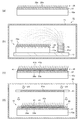
- FIG. 8 is a schematic diagram showing a part of the manufacturing method of the liquid crystal device.
- a method for manufacturing the liquid crystal device will be described with reference to FIGS.
- step S11 a manufacturing method on the element substrate 10 side will be described.
- the first base material 10a to the third interlayer insulating layer 11d will be described as the first base material 10a.
- step S11 the pixel electrode 27 and the like are formed on the first base material 10a made of a glass substrate or the like using a well-known film forming technique, photolithography technique, and etching technique.
- step S12 inorganic alignment film forming step
- the first inorganic alignment film 28 is formed. Specifically, as shown in FIG. 8A, an inorganic material such as silicon oxide is obliquely deposited on the entire third interlayer insulating layer 11d (first base material 10a) provided with the pixel electrode 27. As a result, the first inorganic alignment film 28 having the columnar structures 28a is formed.
- step S13 surface layer forming step
- the surface layer 41 is formed on the first inorganic alignment film 28.
- chemical vapor deposition Chemical Vapor Deposition: hereinafter referred to as CVD
- CVD chemical Vapor Deposition
- the element substrate 10 and the container 72 containing the silane coupling material 41a1 having the liquid alkyl group 41a are placed in the sealed chamber 71 of the vacuum chamber of the CVD apparatus 70.
- the container 72 is heated by the heater 73 to vaporize the silane coupling material 41a1.
- the surface layer 41 provided with the alkyl group 41a is formed on the surface of the pixel electrode 27 and the exposed surface of the third interlayer insulating layer 11d.
- the silanol group on the surface of the first inorganic alignment film 28 reacts with the hydrolyzable group of the silane coupling material 41a1, and the silane coupling material 41a1 adheres, so that as shown in FIG. A surface layer 41 having an alkyl group 41 a is formed on the surface of the inorganic alignment film 28.
- the element substrate 10 is irradiated with ultraviolet (Ultra Violet: UV) to decompose and remove a part of the formed surface layer 41 (alkyl group 41a).
- ultraviolet Ultra Violet: UV
- an ultraviolet irradiation method will be described with reference to FIG.
- the element substrate 10 is placed in a device 80 for irradiating ultraviolet rays. After that, a part of the element substrate 10 is irradiated with ultraviolet rays (Vacuum Ultra Violet: UV) using a photomask 81 having a light shielding portion 81a.
- ultraviolet rays Vauum Ultra Violet: UV
- the surface layer 41 formed on the first inorganic alignment film 28 in the region overlapping with the sealing material 17 from the display region E to a part of the sealing material 14 remains in a plan view, and the surface of the other region Layer 41 (alkyl group 41a) is decomposed and removed.
- the surface layer 41 is removed by directly irradiating the organic functional group of the surface layer 41 by irradiation with vacuum ultraviolet rays, generating active oxygen such as ozone, and oxidizing the surface layer 41 excited by the active oxygen. It is thought to be for the purpose.
- step S21 the counter electrode 31 is formed on the second base material 20a made of a translucent material such as a glass substrate by using a well-known film forming technique, photolithography technique, and etching technique.
- step S22 the second inorganic alignment film 32 is formed on the counter electrode 31.
- the manufacturing method of the second inorganic alignment film 32 is, for example, formed by using the oblique deposition method similarly to the first inorganic alignment film 28 on the element substrate 10 side.
- the surface layer 41 is formed on the second inorganic alignment film 32. Specifically, it is formed by chemical vapor deposition (CVD) as in the element substrate 10 side. Thereafter, the counter substrate 20 is irradiated with ultraviolet rays (UV), and a part of the formed surface layer 41 is decomposed and removed. Specifically, it is formed in the same manner as the element substrate 10 side.
- CVD chemical vapor deposition
- UV ultraviolet rays
- step S31 the sealing material 14 is applied on the element substrate 10. Specifically, for example, the relative positional relationship between the element substrate 10 and a dispenser (also possible with a discharge device) is changed, so that the periphery of the display area E in the element substrate 10 (so as to surround the display area E). The sealing material 14 is applied.
- step S32 bonding step
- the element substrate 10 and the counter substrate 20 are bonded together.
- the element substrate 10 and the counter substrate 20 are bonded to the element substrate 10 through the applied sealing material 14. More specifically, it is performed while ensuring the positional accuracy in the vertical and horizontal directions of the substrates 10 and 20.
- step S33 injection step, sealing material forming step
- liquid crystal is injected into the structure from the liquid crystal injection port (opening region 14a), and then the liquid crystal injection port is sealed with the sealing material 17.
- the liquid crystal device 100 is completed.
- FIG. 9 is a schematic diagram showing a configuration of a projection display device including the above-described liquid crystal device.
- the projection display apparatus 1000 of the present embodiment includes a polarization illumination device 1100 arranged along the system optical axis L, two dichroic mirrors 1104 and 1105 as light separation elements, and three Reflective mirrors 1106, 1107, 1108, five relay lenses 1201, 1202, 1203, 1204, 1205, three transmissive liquid crystal light valves 1210, 1220, 1230 as light modulation means, and a cross dichroic as a light combiner A prism 1206 and a projection lens 1207 are provided.
- the polarized light illumination device 1100 is roughly composed of a lamp unit 1101 as a light source composed of a white light source such as an ultra-high pressure mercury lamp or a halogen lamp, an integrator lens 1102, and a polarization conversion element 1103.
- a lamp unit 1101 as a light source composed of a white light source such as an ultra-high pressure mercury lamp or a halogen lamp
- an integrator lens 1102 and a polarization conversion element 1103.
- the dichroic mirror 1104 reflects red light (R) and transmits green light (G) and blue light (B) among the polarized light beams emitted from the polarization illumination device 1100.
- Another dichroic mirror 1105 reflects the green light (G) transmitted through the dichroic mirror 1104 and transmits the blue light (B).
- the red light (R) reflected by the dichroic mirror 1104 is reflected by the reflecting mirror 1106 and then enters the liquid crystal light valve 1210 via the relay lens 1205.
- Green light (G) reflected by the dichroic mirror 1105 enters the liquid crystal light valve 1220 via the relay lens 1204.
- the blue light (B) transmitted through the dichroic mirror 1105 enters the liquid crystal light valve 1230 via a light guide system including three relay lenses 1201, 1202, 1203 and two reflection mirrors 1107, 1108.
- the liquid crystal light valves 1210, 1220, and 1230 are arranged to face the incident surfaces of the cross dichroic prism 1206 for each color light.
- the color light incident on the liquid crystal light valves 1210, 1220, and 1230 is modulated based on video information (video signal) and emitted toward the cross dichroic prism 1206.
- This prism has four right angle prisms bonded together, and a dielectric multilayer film reflecting red light and a dielectric multilayer film reflecting blue light are formed in a cross shape on the inner surface.
- the three color lights are synthesized by these dielectric multilayer films, and the light representing the color image is synthesized.
- the synthesized light is projected on the screen 1300 by the projection lens 1207 which is a projection optical system, and the image is enlarged and displayed.
- the liquid crystal light valve 1210 is one to which the liquid crystal device 100 described above is applied.
- the liquid crystal device 100 is arranged with a gap between a pair of polarizing elements arranged in crossed Nicols on the incident side and the emission side of colored light. The same applies to the other liquid crystal light valves 1220 and 1230.
- liquid crystal device 100 in which image sticking or the like is suppressed is used as the liquid crystal light valves 1210, 1220, and 1230, high display quality can be realized.
- a head-up display a smartphone, an EVF (Electrical View Finder), a mobile mini projector, a mobile phone, a mobile computer, a digital camera, a digital video It can be used for various electronic devices such as cameras, displays, in-vehicle devices, audio devices, exposure devices, and lighting devices.
- EVF Electronic View Finder
- the liquid crystal device 100 of the present embodiment As described above in detail, according to the liquid crystal device 100 of the present embodiment, the method for manufacturing the liquid crystal device 100, and the electronic apparatus, the following effects can be obtained.
- the columnar structure 28 a (column) constituting the first inorganic alignment film 28. It is possible to make the element substrate 10 uneven by following the unevenness. Therefore, when the sealing material 17 is provided in the opening region 14 a on the element substrate 10, the contact area with the sealing material 17 can be increased by the unevenness on the element substrate 10. It can suppress peeling. In addition, since the sealing material 17 is sealed in a wet state in which liquid crystal is put in the area surrounded by the sealing material 14, the adhesiveness becomes stricter. However, the adhesion between the element substrate 10 and the sealing material 14 can be improved by extending the region of the first inorganic alignment film 28 to the region of the sealing material 17.
- the liquid crystal device 100 of the present embodiment since the surface layer 41 is provided on the surface of the first inorganic alignment film 28, the light resistance can be improved, and the liquid crystal device 100 is irradiated with strong light. Can do.
- the first inorganic alignment film 28 is formed under the sealing material 17, and therefore the columnar structures 28 a (columns) constituting the first inorganic alignment film 28. ),
- the element substrate 10 can be made uneven. Therefore, when the sealing material 17 is formed in the opening region 14 a on the element substrate 10, the contact area with the sealing material 17 can be increased by the unevenness on the element substrate 10, and the sealing material 17 is removed from the element substrate 10. It can suppress peeling.
- the first inorganic alignment film 28 is provided so as to extend to a region overlapping the sealing material 17 on the first base material 10a and a region overlapping a part of the sealing material 14.
- the first inorganic alignment film 28 is formed over the entire region of the first base material 10 a that overlaps the sealing material 14 and the sealing material 17 in plan view. It may be provided. According to this, since the 1st inorganic alignment film 28 is provided in the substantially whole on the 1st base material 10a, even when manufacturing using a mask, manufacture can be made easy.
- the surface layer 41 is not provided between the sealing material 17 and the first inorganic alignment film 28, and the surface layer 41 is not provided as long as the liquid crystal device 100 is not irradiated with strong light. It may be configured.
- the present invention is not limited to the transmissive liquid crystal device 100.
- the present invention may be applied to a reflective liquid crystal device.
Landscapes
- Physics & Mathematics (AREA)
- Nonlinear Science (AREA)
- Mathematical Physics (AREA)
- Chemical & Material Sciences (AREA)
- Crystallography & Structural Chemistry (AREA)
- General Physics & Mathematics (AREA)
- Optics & Photonics (AREA)
- Spectroscopy & Molecular Physics (AREA)
- Liquid Crystal (AREA)
Abstract
Description
図1は、液晶装置の構成を示す模式平面図である。図2は、図1に示す液晶装置のH-H’線に沿う模式断面図である。図3は、液晶装置の電気的な構成を示す等価回路図である。以下、液晶装置の構成を、図1~図3を参照しながら説明する。
図5は、液晶装置のうち主に無機配向膜及びシール材及び封止材の構成を示す模式平面図である。図6は、図5に示す液晶装置のA-A’線に沿う模式断面図である。以下、液晶装置のうち主に無機配向膜及びシール材及び封止材の平面的に重なる領域について、図5及び図6を参照しながら説明する。なお、第1基材10aから第3層間絶縁層11dまでを第1基材10aと称して説明する。
図7は、液晶装置の製造方法を工程順に示すフローチャートである。図8は、液晶装置の製造方法のうち一部の製造方法を示す模式図である。以下、液晶装置の製造方法を、図7及び図8を参照しながら説明する。
次に、本実施形態の電子機器としての投射型表示装置について、図9を参照して説明する。図9は、上記した液晶装置を備えた投射型表示装置の構成を示す概略図である。
上記したように、第1基材10a上における封止材17と重なる領域、及び、シール材14の一部と重なる領域に延在して第1無機配向膜28が設けられていることに限定されず、例えば、図10に示す液晶装置200のように、第1基材10a上における、シール材14及び封止材17と平面視で重なる領域の全体に亘って第1無機配向膜28が設けられるようにしてもよい。これによれば、第1基材10a上の略全体に第1無機配向膜28を設けるので、マスクを用いて製造する場合でも、製造を容易にすることができる。
上記したように、封止材17と第1無機配向膜28の間に表面層41を設けることに限定されず、液晶装置100に強い光を照射しない場合であれば、表面層41を設けない構成にしてもよい。
上記したように、透過型の液晶装置100であることに限定されず、例えば、反射型の液晶装置に本発明を適用するようにしてもよい。
Claims (11)
- 第1基板と、
前記第1基板に対向配置された第2基板と、
前記第1基板と前記第2基板との間に配置されるシール材と、
前記第1基板と前記第2基板との間に配置される液晶層と、
前記シール材の開口領域において前記液晶層を封止する封止材と、
前記第1基板と前記液晶層との間に配置された第1無機配向膜と、
前記第2基板と前記液晶層との間に配置された第2無機配向膜と、
を含み、
前記第1無機配向膜は、前記第2基板の側から見たとき、前記封止材が配置される領域の少なくとも一部と重なる領域に配置されていることを特徴とする液晶装置。 - 請求項1に記載の液晶装置であって、
前記第1無機配向膜は、前記第2基板の側から見たとき、前記封止材が配置される領域が含まれるように配置されていることを特徴とする液晶装置。 - 請求項1又は請求項2に記載の液晶装置であって、
前記第1無機配向膜は、前記第2基板の側から見たとき、前記シール材が配置される領域の少なくとも一部と重なるように配置されていることを特徴とする液晶装置。 - 請求項1乃至請求項3のいずれか一項に記載の液晶装置であって、
前記第1無機配向膜と前記封止材との間には表面層が配置されていることを特徴とする液晶装置。 - 第1基板と、
前記第1基板と液晶層との間に配置される第1無機配向膜と、
を含み、
前記第1無機配向膜は、前記液晶層の側から見たとき、シール材の開口領域において前記液晶層を封止する封止材が配置される領域の少なくとも一部と重なる領域に配置されることを特徴とする液晶装置。 - 請求項5に記載の液晶装置であって、
前記第1無機配向膜は、前記液晶層の側から見たとき、前記封止材が配置される領域が含まれるように配置されることを特徴とする液晶装置。 - 請求項5又は請求項6に記載の液晶装置であって、
前記第1無機配向膜は、前記液晶層の側から見たとき、前記シール材が配置される領域の少なくとも一部と重なるように配置されることを特徴とする液晶装置。 - 請求項5乃至請求項7のいずれか一項に記載の液晶装置であって、
前記第1無機配向膜と前記封止材との間には表面層が配置されることを特徴とする液晶装置。 - 第1基板の上に第1無機配向膜を形成する無機配向膜形成工程と、
前記第1基板の上にシール材を形成するシール材形成工程と、
前記シール材を介して前記第1基板と、第2無機配向膜が形成された第2基板と、を貼り合わせる貼り合わせ工程と、
前記シール材の開口領域から前記第1基板と前記第2基板との間に液晶を注入する注入工程と、
前記開口領域において前記液晶を封止する封止材を形成する封止材形成工程と、
を含み、
前記第1無機配向膜は、前記第2基板の側から見たとき、前記封止材が配置される領域の少なくとも一部と重なる領域に配置されていることを特徴とする液晶装置の製造方法。 - 請求項9に記載の液晶装置の製造方法であって、
前記第1無機配向膜の表面に表面処理を施す表面処理工程を有することを特徴とする液晶装置の製造方法。 - 請求項1乃至請求項8のいずれか一項に記載の液晶装置を備えることを特徴とする電子機器。
Priority Applications (2)
| Application Number | Priority Date | Filing Date | Title |
|---|---|---|---|
| CN201480008449.0A CN105026994B (zh) | 2013-02-25 | 2014-02-20 | 液晶装置及其制造方法和电子设备 |
| US14/765,804 US10001675B2 (en) | 2013-02-25 | 2014-02-20 | Liquid crystal device, method of manufacturing liquid crystal device, and electronic apparatus |
Applications Claiming Priority (2)
| Application Number | Priority Date | Filing Date | Title |
|---|---|---|---|
| JP2013034263A JP6221254B2 (ja) | 2013-02-25 | 2013-02-25 | 液晶装置、液晶装置の製造方法、及び電子機器 |
| JP2013-034263 | 2013-02-25 |
Publications (1)
| Publication Number | Publication Date |
|---|---|
| WO2014129191A1 true WO2014129191A1 (ja) | 2014-08-28 |
Family
ID=51390989
Family Applications (1)
| Application Number | Title | Priority Date | Filing Date |
|---|---|---|---|
| PCT/JP2014/000880 Ceased WO2014129191A1 (ja) | 2013-02-25 | 2014-02-20 | 液晶装置、液晶装置の製造方法、及び電子機器 |
Country Status (4)
| Country | Link |
|---|---|
| US (1) | US10001675B2 (ja) |
| JP (1) | JP6221254B2 (ja) |
| CN (1) | CN105026994B (ja) |
| WO (1) | WO2014129191A1 (ja) |
Families Citing this family (3)
| Publication number | Priority date | Publication date | Assignee | Title |
|---|---|---|---|---|
| CN105093646B (zh) * | 2015-08-11 | 2019-03-15 | 京东方科技集团股份有限公司 | 具有无机覆盖层的彩色滤光片基板以及包含它的显示面板 |
| CN108319080B (zh) * | 2018-02-24 | 2021-02-26 | 惠科股份有限公司 | 显示基板及其制造方法和显示面板 |
| US10890807B2 (en) | 2018-02-24 | 2021-01-12 | HKC Corporation Limited | Display substrate, manufacturing method of the display substrate, and display panel |
Citations (3)
| Publication number | Priority date | Publication date | Assignee | Title |
|---|---|---|---|---|
| JP2007093672A (ja) * | 2005-09-27 | 2007-04-12 | Seiko Epson Corp | 電気光学装置及びその製造方法並びに電子機器 |
| JP2008083325A (ja) * | 2006-09-27 | 2008-04-10 | Seiko Epson Corp | 電気光学装置、電気光学装置の製造方法、及び電子機器 |
| JP2011174966A (ja) * | 2010-02-23 | 2011-09-08 | Seiko Epson Corp | 液晶表示装置の製造方法 |
Family Cites Families (16)
| Publication number | Priority date | Publication date | Assignee | Title |
|---|---|---|---|---|
| JP2000047211A (ja) * | 1998-07-31 | 2000-02-18 | Sony Corp | 液晶素子及びその製造方法 |
| JP4077182B2 (ja) * | 2001-10-11 | 2008-04-16 | 株式会社日立製作所 | 液晶表示装置 |
| JP4396208B2 (ja) | 2003-10-01 | 2010-01-13 | ソニー株式会社 | 液晶表示素子および液晶表示素子の製造方法 |
| KR100733522B1 (ko) * | 2004-05-28 | 2007-06-28 | 도시바 마쯔시따 디스플레이 테크놀로지 컴퍼니, 리미티드 | 액정 표시 패널 |
| JP2006119403A (ja) * | 2004-10-22 | 2006-05-11 | Seiko Epson Corp | 電気光学装置及びその製造方法、並びに電子機器 |
| JP2006119401A (ja) * | 2004-10-22 | 2006-05-11 | Seiko Epson Corp | 電気光学装置の製造方法及び製造装置、電気光学装置並びに電子機器 |
| JP4201002B2 (ja) * | 2005-03-28 | 2008-12-24 | セイコーエプソン株式会社 | 液晶装置、その製造方法およびプロジェクタ |
| JP4670452B2 (ja) * | 2005-04-19 | 2011-04-13 | セイコーエプソン株式会社 | 液晶パネルの製造方法 |
| JP4297088B2 (ja) * | 2005-07-04 | 2009-07-15 | セイコーエプソン株式会社 | 電気光学装置及びその製造方法、並びに電子機器 |
| CN1908777A (zh) * | 2005-08-05 | 2007-02-07 | 精工爱普生株式会社 | 液晶装置、电子光学装置、投影仪及微型器件 |
| JP2007108371A (ja) | 2005-10-13 | 2007-04-26 | Seiko Epson Corp | 液晶パネル、液晶パネルの製造方法および電子機器 |
| JP2009223139A (ja) * | 2008-03-18 | 2009-10-01 | Seiko Epson Corp | 液晶装置及びその製造方法、電子機器 |
| JP2009223138A (ja) * | 2008-03-18 | 2009-10-01 | Seiko Epson Corp | 液晶装置及びその製造方法、電子機器 |
| JP4640462B2 (ja) * | 2008-07-10 | 2011-03-02 | セイコーエプソン株式会社 | 液晶装置の製造方法 |
| JP5187067B2 (ja) * | 2008-08-20 | 2013-04-24 | セイコーエプソン株式会社 | 電気光学装置及び電子機器 |
| JP2012088470A (ja) * | 2010-10-19 | 2012-05-10 | Seiko Epson Corp | 液晶表示素子の製造方法及び液晶表示素子 |
-
2013
- 2013-02-25 JP JP2013034263A patent/JP6221254B2/ja active Active
-
2014
- 2014-02-20 WO PCT/JP2014/000880 patent/WO2014129191A1/ja not_active Ceased
- 2014-02-20 US US14/765,804 patent/US10001675B2/en active Active
- 2014-02-20 CN CN201480008449.0A patent/CN105026994B/zh active Active
Patent Citations (3)
| Publication number | Priority date | Publication date | Assignee | Title |
|---|---|---|---|---|
| JP2007093672A (ja) * | 2005-09-27 | 2007-04-12 | Seiko Epson Corp | 電気光学装置及びその製造方法並びに電子機器 |
| JP2008083325A (ja) * | 2006-09-27 | 2008-04-10 | Seiko Epson Corp | 電気光学装置、電気光学装置の製造方法、及び電子機器 |
| JP2011174966A (ja) * | 2010-02-23 | 2011-09-08 | Seiko Epson Corp | 液晶表示装置の製造方法 |
Also Published As
| Publication number | Publication date |
|---|---|
| JP6221254B2 (ja) | 2017-11-01 |
| CN105026994A (zh) | 2015-11-04 |
| CN105026994B (zh) | 2018-05-08 |
| JP2014164071A (ja) | 2014-09-08 |
| US20150370106A1 (en) | 2015-12-24 |
| US10001675B2 (en) | 2018-06-19 |
Similar Documents
| Publication | Publication Date | Title |
|---|---|---|
| JP6361327B2 (ja) | 電気光学装置、及び電子機器 | |
| JP6251955B2 (ja) | 電気光学装置、電気光学装置の製造方法、及び電子機器 | |
| JP6123250B2 (ja) | 液晶装置、液晶装置の製造方法、及び電子機器 | |
| JP2013235128A (ja) | 電気光学装置の製造方法、及び電気光学装置用基板 | |
| JP6221254B2 (ja) | 液晶装置、液晶装置の製造方法、及び電子機器 | |
| JP6263944B2 (ja) | 液晶装置、液晶装置の製造方法、及び電子機器 | |
| JP5919890B2 (ja) | 電気光学装置、及び電子機器 | |
| JP2013182144A (ja) | 電気光学装置、及び電子機器 | |
| JP6635099B2 (ja) | 液晶装置及び電子機器 | |
| JP2015055816A (ja) | 電気光学装置用基板、電気光学装置用基板の製造方法、電気光学装置、及び電子機器 | |
| JP2014182251A (ja) | 電気光学装置、電気光学装置の製造方法、及び電子機器 | |
| JP6191293B2 (ja) | 表面処理方法、及び電気光学装置の製造方法 | |
| JP2014157303A (ja) | 液晶装置の製造方法 | |
| JP2015132703A (ja) | 液晶装置、液晶装置の製造方法、及び電子機器 | |
| JP6236827B2 (ja) | 電気光学装置、電気光学装置の製造方法、及び電子機器 | |
| JP2014085518A (ja) | 液晶装置の製造方法 | |
| JP2014077818A (ja) | 液晶装置、液晶装置の製造方法、及び電子機器 | |
| JP6277640B2 (ja) | 電気光学装置用基板の製造方法、電気光学装置用基板、電気光学装置、及び電子機器 | |
| JP6361155B2 (ja) | 電気光学装置、電気光学装置の製造方法、及び電子機器 | |
| JP2014026142A (ja) | 液晶装置の製造方法、液晶装置、及び電子機器 | |
| JP2014119683A (ja) | 液晶装置、及び電子機器 | |
| JP2015210465A (ja) | 液晶装置の製造方法 | |
| JP2014142385A (ja) | 電気光学装置、電気光学装置の製造方法、及び電子機器 | |
| JP2014224890A (ja) | 電気光学装置の製造方法、電気光学装置、及び電子機器 | |
| JP2015200692A (ja) | 電気光学装置、電気光学装置の製造方法、及び電子機器 |
Legal Events
| Date | Code | Title | Description |
|---|---|---|---|
| WWE | Wipo information: entry into national phase |
Ref document number: 201480008449.0 Country of ref document: CN |
|
| 121 | Ep: the epo has been informed by wipo that ep was designated in this application |
Ref document number: 14753697 Country of ref document: EP Kind code of ref document: A1 |
|
| WWE | Wipo information: entry into national phase |
Ref document number: 14765804 Country of ref document: US |
|
| NENP | Non-entry into the national phase |
Ref country code: DE |
|
| 122 | Ep: pct application non-entry in european phase |
Ref document number: 14753697 Country of ref document: EP Kind code of ref document: A1 |