WO2014125893A1 - クリーニングガス及びクリーニング方法 - Google Patents
クリーニングガス及びクリーニング方法 Download PDFInfo
- Publication number
- WO2014125893A1 WO2014125893A1 PCT/JP2014/051453 JP2014051453W WO2014125893A1 WO 2014125893 A1 WO2014125893 A1 WO 2014125893A1 JP 2014051453 W JP2014051453 W JP 2014051453W WO 2014125893 A1 WO2014125893 A1 WO 2014125893A1
- Authority
- WO
- WIPO (PCT)
- Prior art keywords
- cleaning
- silicon carbide
- gas
- graphite
- iodine heptafluoride
- Prior art date
- Legal status (The legal status is an assumption and is not a legal conclusion. Google has not performed a legal analysis and makes no representation as to the accuracy of the status listed.)
- Ceased
Links
Images
Classifications
-
- C—CHEMISTRY; METALLURGY
- C11—ANIMAL OR VEGETABLE OILS, FATS, FATTY SUBSTANCES OR WAXES; FATTY ACIDS THEREFROM; DETERGENTS; CANDLES
- C11D—DETERGENT COMPOSITIONS; USE OF SINGLE SUBSTANCES AS DETERGENTS; SOAP OR SOAP-MAKING; RESIN SOAPS; RECOVERY OF GLYCEROL
- C11D7/00—Compositions of detergents based essentially on non-surface-active compounds
- C11D7/02—Inorganic compounds
- C11D7/04—Water-soluble compounds
-
- C—CHEMISTRY; METALLURGY
- C23—COATING METALLIC MATERIAL; COATING MATERIAL WITH METALLIC MATERIAL; CHEMICAL SURFACE TREATMENT; DIFFUSION TREATMENT OF METALLIC MATERIAL; COATING BY VACUUM EVAPORATION, BY SPUTTERING, BY ION IMPLANTATION OR BY CHEMICAL VAPOUR DEPOSITION, IN GENERAL; INHIBITING CORROSION OF METALLIC MATERIAL OR INCRUSTATION IN GENERAL
- C23C—COATING METALLIC MATERIAL; COATING MATERIAL WITH METALLIC MATERIAL; SURFACE TREATMENT OF METALLIC MATERIAL BY DIFFUSION INTO THE SURFACE, BY CHEMICAL CONVERSION OR SUBSTITUTION; COATING BY VACUUM EVAPORATION, BY SPUTTERING, BY ION IMPLANTATION OR BY CHEMICAL VAPOUR DEPOSITION, IN GENERAL
- C23C16/00—Chemical coating by decomposition of gaseous compounds, without leaving reaction products of surface material in the coating, i.e. chemical vapour deposition [CVD] processes
- C23C16/22—Chemical coating by decomposition of gaseous compounds, without leaving reaction products of surface material in the coating, i.e. chemical vapour deposition [CVD] processes characterised by the deposition of inorganic material, other than metallic material
- C23C16/30—Deposition of compounds, mixtures or solid solutions, e.g. borides, carbides, nitrides
- C23C16/32—Carbides
- C23C16/325—Silicon carbide
-
- B—PERFORMING OPERATIONS; TRANSPORTING
- B08—CLEANING
- B08B—CLEANING IN GENERAL; PREVENTION OF FOULING IN GENERAL
- B08B7/00—Cleaning by methods not provided for in a single other subclass or a single group in this subclass
- B08B7/0064—Cleaning by methods not provided for in a single other subclass or a single group in this subclass by temperature changes
- B08B7/0071—Cleaning by methods not provided for in a single other subclass or a single group in this subclass by temperature changes by heating
-
- C—CHEMISTRY; METALLURGY
- C11—ANIMAL OR VEGETABLE OILS, FATS, FATTY SUBSTANCES OR WAXES; FATTY ACIDS THEREFROM; DETERGENTS; CANDLES
- C11D—DETERGENT COMPOSITIONS; USE OF SINGLE SUBSTANCES AS DETERGENTS; SOAP OR SOAP-MAKING; RESIN SOAPS; RECOVERY OF GLYCEROL
- C11D7/00—Compositions of detergents based essentially on non-surface-active compounds
- C11D7/02—Inorganic compounds
-
- C—CHEMISTRY; METALLURGY
- C23—COATING METALLIC MATERIAL; COATING MATERIAL WITH METALLIC MATERIAL; CHEMICAL SURFACE TREATMENT; DIFFUSION TREATMENT OF METALLIC MATERIAL; COATING BY VACUUM EVAPORATION, BY SPUTTERING, BY ION IMPLANTATION OR BY CHEMICAL VAPOUR DEPOSITION, IN GENERAL; INHIBITING CORROSION OF METALLIC MATERIAL OR INCRUSTATION IN GENERAL
- C23C—COATING METALLIC MATERIAL; COATING MATERIAL WITH METALLIC MATERIAL; SURFACE TREATMENT OF METALLIC MATERIAL BY DIFFUSION INTO THE SURFACE, BY CHEMICAL CONVERSION OR SUBSTITUTION; COATING BY VACUUM EVAPORATION, BY SPUTTERING, BY ION IMPLANTATION OR BY CHEMICAL VAPOUR DEPOSITION, IN GENERAL
- C23C16/00—Chemical coating by decomposition of gaseous compounds, without leaving reaction products of surface material in the coating, i.e. chemical vapour deposition [CVD] processes
- C23C16/44—Chemical coating by decomposition of gaseous compounds, without leaving reaction products of surface material in the coating, i.e. chemical vapour deposition [CVD] processes characterised by the method of coating
- C23C16/4401—Means for minimising impurities, e.g. dust, moisture or residual gas, in the reaction chamber
- C23C16/4405—Cleaning of reactor or parts inside the reactor by using reactive gases
-
- H—ELECTRICITY
- H01—ELECTRIC ELEMENTS
- H01J—ELECTRIC DISCHARGE TUBES OR DISCHARGE LAMPS
- H01J37/00—Discharge tubes with provision for introducing objects or material to be exposed to the discharge, e.g. for the purpose of examination or processing thereof
- H01J37/32—Gas-filled discharge tubes
- H01J37/32431—Constructional details of the reactor
- H01J37/32798—Further details of plasma apparatus not provided for in groups H01J37/3244 - H01J37/32788; special provisions for cleaning or maintenance of the apparatus
- H01J37/32853—Hygiene
- H01J37/32862—In situ cleaning of vessels and/or internal parts
-
- C—CHEMISTRY; METALLURGY
- C11—ANIMAL OR VEGETABLE OILS, FATS, FATTY SUBSTANCES OR WAXES; FATTY ACIDS THEREFROM; DETERGENTS; CANDLES
- C11D—DETERGENT COMPOSITIONS; USE OF SINGLE SUBSTANCES AS DETERGENTS; SOAP OR SOAP-MAKING; RESIN SOAPS; RECOVERY OF GLYCEROL
- C11D2111/00—Cleaning compositions characterised by the objects to be cleaned; Cleaning compositions characterised by non-standard cleaning or washing processes
- C11D2111/10—Objects to be cleaned
- C11D2111/14—Hard surfaces
- C11D2111/20—Industrial or commercial equipment, e.g. reactors, tubes or engines
Definitions
- the present invention relates to a cleaning gas and a cleaning method for removing deposits containing silicon carbide deposited on a substrate.
- Silicon carbide (SiC) is used in many fields as an important ceramic material. In recent years, silicon carbide epitaxial growth technology has attracted attention. In particular, applications such as transistors with low power consumption have been developed because of their high dielectric breakdown voltage and reliability during high-temperature operation.
- ⁇ ⁇ Silicon carbide used for such applications needs to be a single crystal of high purity.
- a chemical vapor deposition method (Chemical Vapor Deposition method) is used to grow a film by a chemical reaction such as propane gas and silane gas, or monomethylsilane is used as a raw material for the CVD method. Methods for growing are known.
- silicon carbide adheres to and accumulates on unintended parts such as the inner wall of a graphite reaction vessel and a susceptor.
- the silicon carbide fine particles deposited on these unintended portions sometimes peel off and drop off, and drop and adhere to the growth surface of the silicon carbide thin film, thereby inhibiting crystal growth and causing defects. Therefore, the silicon carbide deposited on the inner wall of the reaction vessel must be periodically removed.
- the removal method conventionally, when silicon carbide is deposited on the inner wall of the reaction vessel, a method of peeling off with a tool or periodically replacing the vessel has been adopted.
- Patent Documents 1 and 2 disclose a semiconductor manufacturing apparatus that forms a SiC epitaxial film on a wafer placed on a susceptor.
- a cleaning gas for removing the SiC film attached to the susceptor chlorine trifluoride ( The use of a gas containing ClF 3 ) is described.
- Patent Document 3 discloses a method of etching a surface of silicon carbide by bringing chlorine trifluoride gas into contact with the surface of silicon carbide.
- the chlorine trifluoride gas disclosed in Patent Documents 1 to 3 is an excellent cleaning gas that does not require plasma excitation and can efficiently remove silicon carbide only by thermal excitation such as heating.
- chlorine trifluoride has a problem that the material of the reaction vessel is limited because of its high reactivity such as corrosion. A material that does not react to the above is used.
- Chlorine trifluoride is easy to react with graphite. Therefore, when chlorine trifluoride gas is used to clean the graphite reaction vessel and susceptor that make up the SiC film-forming device, only the silicon carbide that is the target for removal is removed. However, the surface of the graphite constituting the reaction vessel and the susceptor is removed and the graphite is damaged.
- Patent Documents 1 and 2 used graphite reactors and susceptors in which the surface of graphite was coated with silicon carbide (SiC) by the CVD method.
- SiC silicon carbide
- the present invention has been made in view of the above problems, and in the cleaning process of deposits containing silicon carbide deposited on a substrate containing graphite material, without etching and damaging the graphite,
- An object of the present invention is to provide a cleaning gas and a cleaning method capable of removing silicon carbide at a sufficient cleaning rate of silicon carbide.
- the inventors of the present invention brought a gas containing iodine heptafluoride into contact with silicon carbide deposited on a base material made of carbon having a graphite structure.
- the inventors have found that silicon carbide can be removed preferentially with respect to graphite without causing significant damage by etching, and have reached the present invention.
- the present invention is a cleaning gas containing iodine heptafluoride for removing deposits containing silicon carbide deposited on a substrate made of carbon having a graphite structure at least partially.
- At least one gas selected from the group consisting of F 2 , ClF 3 , COF 2 , O 2 , O 3 , NO, NO 2 , N 2 O and N 2 O 4 is further used as the oxidizing gas. May be included.
- the inert gas may further include at least one selected from the group consisting of He, Ne, Ar, Xe, Kr and N 2 .
- the base material is an inner wall of an apparatus for manufacturing a silicon carbide single crystal manufactured at a high temperature of 1500 ° C. or higher, or an accessory thereof.
- the apparatus for producing the silicon carbide single crystal is a thin film forming apparatus for forming a silicon carbide single crystal, and the thin film forming apparatus is particularly preferably a silicon carbide epitaxial film forming apparatus.
- the accessory device is preferably a susceptor for installing a semiconductor wafer.
- the present invention is also a cleaning method for removing deposits containing silicon carbide deposited on a base material while heating the base material using the cleaning gas described above.
- a deposit containing silicon carbide deposited on a base material made of carbon having a graphite structure can be sufficiently cleaned without etching and damaging the graphite constituting the base material. Can be removed efficiently.
- the cleaning method using the cleaning gas of the present invention has an excellent silicon carbide cleaning speed as compared with the conventional method, so that the cleaning time is short, the influence on the graphite is not concerned, and the graphite is damaged. Can be greatly reduced.
- the cleaning gas of the present invention contains iodine heptafluoride (hereinafter sometimes simply referred to as IF 7 ), and contains silicon carbide deposited at least partially on a base material made of carbon having a graphite structure. It is intended for deposits, and is characterized by removing deposits without damaging the substrate.
- IF 7 iodine heptafluoride
- Iodine heptafluoride (IF 7 ) used in the present invention is manufactured on an industrial scale and can be purchased and used, and is not particularly limited. Further, IF 7 can be obtained by a conventionally known production method, for example, can be produced and obtained by a production method proposed in Japanese Patent Application Laid-Open No. 2009-23896 related to the applicant's application.
- the cleaning gas of the present invention is usually used in a content of iodine heptafluoride in the range of 1 to 100% by volume, preferably 10 to 100% by volume.
- iodine heptafluoride can be used alone, various additives can be appropriately added depending on the purpose.
- an oxidizing gas can be added as an additive in order to adjust the cleaning performance.
- the oxidizing gas is added to improve the cleaning speed.
- the inert gas is added to reduce the cost of the cleaning gas used and to adjust the cleaning speed.
- oxygen-containing gases such as O 2 , O 3 , CO 2 , COCl 2 , COF 2 , N 2 O, NO, NO 2 , F 2 , NF 3 , Cl 2 , Br 2 , I 2.
- O 2 , N 2 O, NO, COF 2 , F 2 , NF 3 , and Cl 2 are preferable.
- O 2 , N 2 O, and NO are effective in improving the cleaning rate (Examples). reference).
- a gas generally used as a cleaning gas such as perfluorocarbons is added in a range of 1 to 99% by volume in the cleaning gas composition within a range not impairing the effect of the cleaning gas of the present invention.
- the gas include F 6 , C 5 F 8 , and C 5 F 10 .
- the cleaning gas of the present invention can be added with an inert gas such as N 2 , He, Ar, Ne, Kr, etc., as appropriate, together with the above-described oxidizing gas.
- an inert gas such as N 2 , He, Ar, Ne, Kr, etc.
- concentration is not limited, but is usually 1 to 99% by volume, preferably 5 to 50% by volume in the cleaning gas composition. Used at a content of about%.
- the deposit targeted by the cleaning gas of the present invention is a deposit containing silicon carbide adhering to the surface of a substrate made of carbon having at least a graphite structure.
- deposit means “unnecessary deposit”.
- the deposit to which the present invention is applied is not particularly limited as long as it contains silicon carbide as a main component in the deposit, and silicon carbide may be a single component.
- CVD method chemical vapor deposition method
- MOCVD method metal organic chemical vapor deposition method
- sputtering method sol-gel method
- sol-gel method vapor deposition method and the like.
- auxiliary equipment such as jigs such as a susceptor and piping for installing an inner wall of a manufacturing apparatus or a semiconductor wafer.
- the present invention can be applied not only to a thin film or a thick film of silicon carbide but also to unnecessary deposits attached to an inner wall of a manufacturing apparatus that performs large bulk crystal growth such as a hexagonal SiC wafer or its accessory parts.
- a sublimation recrystallization method an improved Lerry method in which a silicon carbide raw material is heated and sublimated to grow silicon carbide on a seed crystal to grow a bulk crystal.
- the substrate of the present invention is a substrate made of carbon having at least a part of a graphite structure, and can withstand high temperature conditions of 1500 ° C. or higher in which a graphite single component or the surface of graphite is coated with a protective film such as silicon carbide. It is a substrate. Specifically, it is an article that constitutes the above-described silicon carbide manufacturing apparatus, and examples include an inner wall of the silicon carbide manufacturing apparatus or a jig such as a susceptor for installing a semiconductor wafer, and an auxiliary apparatus such as a pipe. Among these, the cleaning gas of the present invention is suitable for a susceptor for installing an inner wall of a manufacturing apparatus or a semiconductor wafer on which unnecessary deposits are easily deposited.
- the present invention uses a cleaning gas containing iodine heptafluoride and deposits containing silicon carbide formed on the surface of the substrate while heating the substrate with a heater installed outside the reactor. It is the cleaning method which removes. Reaction mechanism that removes unnecessary deposits deposited on the substrate by reaction of fluorine radicals generated by thermal decomposition of iodine heptafluoride used as cleaning gas with silicon (Si) component of silicon carbide in the deposits Is considered.
- the reactivity between the cleaning gas and SiC is considered to be caused by various factors such as chemical properties of the cleaning gas used, such as bond dissociation energy and ionicity.
- bond dissociation energy is considered to be one of the important factors, and it is considered that the lower the bond dissociation energy, the faster the reaction rate with SiC.
- ClF 3 is a fluoride such as IF 7 and IF 5 . Since the bond dissociation energy is lower than that of the iodine compound (see Table 1 below), it is considered that the reactivity with SiC is high.
- F 2 is “Introduction to Fluorochemistry 2010” edited by the Japan Society for the Promotion of Science and Fluorine Chemistry 155 Committee, Sankyo Publishing, 2010, p2, ClF 3, IF 7, Regarding IF 5 , J. C. BAILAR JR., COMREHENSIVE INORGANIC CHEMISTRY, II, PERGAMON PRESS Ltd, 1973, p1491-p1496.
- iodine heptafluoride has a higher reaction rate with silicon carbide than ClF 3 when heated to 150 ° C. or higher in spite of its relatively high bond dissociation energy. Early and unique results were obtained that did not damage the graphite (see Examples below). Although the reaction machine is not clear, the low-order iodine fluoride compound (IF 5 ) produced by thermal decomposition of iodine heptafluoride has a larger molecular size than ClF produced in the case of ClF 3. It is presumed that the molecular size of the object affects the protection of graphite. Regarding the reactivity with silicon carbide, it is presumed that not only fluorine radicals but also iodine fluoride compounds such as IF 7 and IF 5 react with silicon carbide.
- the temperature of the substrate on which the deposit containing silicon carbide is deposited is not particularly limited, but is usually 150 to 700 ° C., preferably 300 to 600 ° C. .
- iodine heptafluoride that does not thermally decompose enters between graphite layers to form a compound and a sufficient cleaning performance may not be obtained.
- a temperature higher than 700 ° C. is not preferable because energy is wasted and running costs such as power consumption are increased.
- the pressure is usually in a reduced pressure state, but it may be under atmospheric pressure and is not particularly limited. When it exceeds 500 ° C., it is preferably 13.3 kPa (100 Torr) or less, and more preferably 6.6 kPa (50 Torr) or less. If it exceeds 13.3 kPa (100 Torr), corrosion occurs and is not preferable. Further, the flow rate of the cleaning gas to be used is appropriately adjusted depending on the reactor capacity of the cleaning device.
- a thermal decomposition method is used from the viewpoint of ease of operation and cost, but a photolysis method or a plasma method may be used as another excitation method. Since the cleaning gas of the present invention can efficiently remove silicon carbide without plasma only by heat treatment, there are few restrictions on the apparatus for making the inside of the apparatus a plasma atmosphere and there is no load on the material of the apparatus. Have advantages.
- an apparatus to be processed of the cleaning method of the present invention it can be applied to a silicon carbide film forming apparatus for forming a thin film such as a semiconductor device or a coating tool, a whisker, a powder or the like by a CVD method.
- the present invention can be applied not only to silicon carbide thin films and thick films but also to unnecessary deposits attached to the inner wall of a manufacturing apparatus that performs large bulk crystal growth such as a hexagonal SiC wafer or its accessory parts.
- application to a film forming apparatus is particularly preferable, and it is particularly preferable to use the film forming apparatus for performing epitaxial film growth of silicon carbide in which film formation is performed under a high temperature condition.
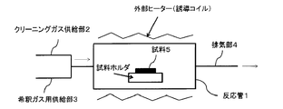
- FIG. 1 shows a schematic diagram of a cleaning device used in Examples and Comparative Examples of the present invention.
- the cleaning apparatus used an externally heated horizontal reactor equipped with a cylindrical reaction tube 1 (made of alumina) as a reaction vessel.
- a gas supply unit 2 for supplying a cleaning gas and a gas supply unit for dilution 3 are connected to the cylindrical reaction tube 1, and an exhaust unit 4 for discharging the gas from the reaction tube is provided downstream of the reaction tube 1.
- an induction heating coil is installed as an external heater on the outer periphery of the reaction tube 1, and the inside of the reaction tube can be heated by this induction coil.
- the cleaning test was performed by setting a single crystal silicon carbide substrate and a graphite plate as sample 5 in the reaction tube.
- a cleaning test was performed by measuring the cleaning rate of silicon carbide using the cleaning gas of the present invention.
- the weight change rate of graphite before and after the cleaning test was examined.
- the weight change rate of graphite was calculated from the amount of change by measuring the weight of the graphite plate before and after cleaning.
- Table 2 shows the cleaning conditions and the results of the weight change rate of graphite in Examples and Comparative Examples.
- the cleaning speed was calculated from the weight change of the sample using the following general formula (3).
- Example 1 A single crystal silicon carbide substrate and a graphite plate (both 0.5 cm in width, 1 cm in length, and 0.5 mm in thickness) prepared by the CVD method are inserted into the reaction vessel as sample test pieces, and placed outside the reaction vessel. While the installed heater was heated to 250 ° C., iodine heptafluoride (IF 7 ) gas was supplied from the gas supply unit 1 at a gas flow rate of 0.1 L / min, and the pressure in the reaction vessel was 6.6 kPa (50 torr). ) For 1 hour. A graphite plate manufactured by Niraco Co., Ltd. (purity 99.99%) was used. As a result, the cleaning rate of silicon carbide was 10 nm / min, and the weight change rate of graphite was 0.02% in 1 hour.
- IF 7 iodine heptafluoride
- Example 2 A cleaning test was conducted under the same conditions as in Example 1 except that the temperature of the reaction vessel was changed to 300 ° C. As a result, the cleaning rate of silicon carbide was 26 nm / min, and the weight change of the graphite plate was 0.10% in 1 hour.
- Example 3 A cleaning test was conducted under the same conditions as in Example 1 except that the temperature of the reaction vessel was 350 ° C. As a result, the cleaning rate of silicon carbide was 56 nm / min, and the weight change of the graphite plate was 0.48% in 1 hour.
- Example 4 A cleaning test was conducted under the same conditions as in Example 1 except that the temperature of the reaction vessel was 400 ° C. As a result, the cleaning rate of silicon carbide was 212 nm / min, and the weight change of the graphite plate was 1.2% in 1 hour.
- Example 5 A cleaning test was conducted under the same conditions as in Example 1 except that the temperature of the reaction vessel was 500 ° C. As a result, the cleaning rate of silicon carbide was 710 nm / min, and the weight change of the graphite plate was 2.2% in 1 hour.
- Example 6 A cleaning test was performed under the same conditions as in Example 4 except that the pressure in the reaction vessel was 101 kPa (760 Torr). As a result, the cleaning rate of silicon carbide was 526 nm / min, and the weight change of the graphite plate was 3.0% in 1 hour.
- Example 7 Cleaning under the same conditions as in Example 4 except that the composition was iodine heptafluoride: 10% by volume and nitrogen (N 2 ): 90% by volume, and the pressure was 66.7 kPa (500 torr). A test was conducted. As a result, the cleaning rate of silicon carbide was 231 nm / min, and the weight change of the graphite plate was 1.6% in 1 hour.
- Example 8 A cleaning test was performed under the same conditions as in Example 3 except that a mixed gas of iodine heptafluoride: 50% by volume and hydrogen fluoride (HF): 50% by volume was used. As a result, the cleaning rate of silicon carbide was 66 nm / min, and the weight change of the graphite plate was 0.36% in 1 hour. From the results of Example 8, it was found that the addition of hydrogen fluoride improves the cleaning rate.
- a mixed gas of iodine heptafluoride 50% by volume
- HF hydrogen fluoride
- Example 9 A cleaning test was performed under the same conditions as in Example 3 except that a mixed gas of iodine heptafluoride: 25% by volume and oxygen (O 2 ): 75% by volume was used. As a result, the cleaning rate of silicon carbide was 195 nm / min, and the weight change of the graphite plate was 0.38% in 1 hour. From the results of Example 9, it was found that the cleaning rate was significantly improved when oxygen was added.
- Example 10 A cleaning test was conducted under the same conditions as in Example 3 except that a mixed gas having a composition of iodine heptafluoride: 50% by volume and oxygen (O 2 ): 50% by volume was used. As a result, the cleaning rate of silicon carbide was 228 nm / min, and the weight change of the graphite plate was 0.45% in 1 hour.
- Example 11 A cleaning test was conducted under the same conditions as in Example 3 except that a mixed gas of iodine heptafluoride: 75% by volume and oxygen (O 2 ): 25% by volume was used. As a result, the cleaning rate of silicon carbide was 179 nm / min, and the weight change of the graphite plate was 0.45% in 1 hour.
- Example 12 A cleaning test was performed under the same conditions as in Example 1 except that the temperature was 200 ° C. As a result, the silicon carbide cleaning rate was inferior to that of the other examples, but almost no change in the weight of graphite was observed.
- Example 13 A cleaning test was performed under the same conditions as in Example 3 except that a mixed gas of iodine heptafluoride: 75% by volume and nitrogen dioxide (NO 2 ): 25% by volume was used. As a result, the cleaning rate of silicon carbide was 141 nm / min, and the weight change of the graphite plate was 0.43% in 1 hour.
- Example 14 A cleaning test was conducted under the same conditions as in Example 3 except that a mixed gas having a composition of iodine heptafluoride: 50% by volume and nitrogen dioxide (NO 2 ): 50% by volume was used. As a result, the cleaning rate of silicon carbide was 151 nm / min, and the weight change of the graphite plate was 0.46% in 1 hour.
- Example 15 A cleaning test was conducted under the same conditions as in Example 3 except that a mixed gas of iodine heptafluoride: 25% by volume and nitrogen dioxide (NO 2 ): 75% by volume was used. As a result, the cleaning rate of silicon carbide was 157 nm / min, and the weight change of the graphite plate was 0.43% in 1 hour.
- Example 16 A cleaning test was performed under the same conditions as in Example 3, except that a mixed gas of iodine heptafluoride: 25% by volume and nitrogen monoxide (NO): 75% by volume was used. As a result, the cleaning rate of silicon carbide was 89 nm / min, and the weight change of the graphite plate was 0.07% in 1 hour.
- Example 17 A cleaning test was performed under the same conditions as in Example 3 except that a mixed gas having a composition of iodine heptafluoride: 50% by volume and nitric oxide (NO): 50% by volume was used. As a result, the cleaning rate of silicon carbide was 879 nm / min, and the weight change of the graphite plate was 0.42% in 1 hour.
- Example 18 A cleaning test was conducted under the same conditions as in Example 3 except that a mixed gas of iodine heptafluoride: 75% by volume and nitrogen monoxide (NO): 25% by volume was used. As a result, the cleaning rate of silicon carbide was 1050 nm / min, and the weight change of the graphite plate was 0.44% in 1 hour.
- Example 1 A cleaning test was performed under the same conditions as in Example 2 except that chlorine trifluoride gas was used instead of iodine heptafluoride gas. As a result, the cleaning rate of silicon carbide is slower than when using 7 nm / min and iodine heptafluoride gas, and the weight change of graphite is 0.1% per hour when using iodine heptafluoride gas. It was big compared.
- Example 2 A cleaning test was conducted under the same conditions as in Example 3 except that chlorine trifluoride gas was used instead of iodine heptafluoride gas. As a result, the cleaning rate of silicon carbide is 30 nm / min, which is slower than when iodine heptafluoride gas is used, and the weight change of graphite is 1% per hour compared with when iodine heptafluoride gas is used. It was big.
- Example 3 A cleaning test was performed under the same conditions as in Example 4 except that chlorine trifluoride gas was used instead of iodine heptafluoride gas. As a result, the cleaning rate of silicon carbide is 93 nm / min, which is slower than that when iodine heptafluoride gas is used, and the weight change of graphite is 2% per hour compared with the case where iodine heptafluoride gas is used. It was big.
- Example 4 A cleaning test was performed under the same conditions as in Example 2 except that fluorine gas was used instead of iodine heptafluoride gas. As a result, the cleaning rate of silicon carbide was 28 nm / min, which was equivalent to iodine heptafluoride gas, but the weight change of graphite was 0.1% per hour, compared with the case where iodine heptafluoride gas was used. It was big.
- Example 5 A cleaning test was performed under the same conditions as in Example 3 except that fluorine gas was used instead of iodine heptafluoride gas. As a result, the cleaning rate of silicon carbide was 146 nm / min, which was higher than iodine heptafluoride gas, but the weight change of graphite was 2% in 1 hour, which was larger than when using iodine heptafluoride gas.
- Example 6 A cleaning test was conducted under the same conditions as in Example 4 except that fluorine gas was used instead of iodine heptafluoride gas. As a result, the cleaning rate of silicon carbide was 350 nm / min and more than iodine heptafluoride gas, but the weight change of graphite was 3% in 1 hour, which was larger than when using iodine heptafluoride gas. It was.
- iodine heptafluoride (IF 7 ) has better cleaning performance than other halogen fluoride gas (ClF 3 ) and fluorine gas. And no significant damage (not etched) to the graphite. Therefore, iodine heptafluoride (IF 7 ) has been found to be an excellent cleaning gas for selectively removing silicon carbide deposits without damaging the graphite.
- the cleaning gas and the cleaning method of the present invention are useful for removing unnecessary deposits of silicon carbide manufacturing equipment such as silicon carbide epitaxial film growth and large bulk crystals of silicon carbide.
Landscapes
- Chemical & Material Sciences (AREA)
- Engineering & Computer Science (AREA)
- Chemical Kinetics & Catalysis (AREA)
- Organic Chemistry (AREA)
- Inorganic Chemistry (AREA)
- General Chemical & Material Sciences (AREA)
- Materials Engineering (AREA)
- Mechanical Engineering (AREA)
- Metallurgy (AREA)
- Oil, Petroleum & Natural Gas (AREA)
- Life Sciences & Earth Sciences (AREA)
- Wood Science & Technology (AREA)
- Health & Medical Sciences (AREA)
- Epidemiology (AREA)
- Public Health (AREA)
- Physics & Mathematics (AREA)
- Plasma & Fusion (AREA)
- Analytical Chemistry (AREA)
- Chemical Vapour Deposition (AREA)
- Drying Of Semiconductors (AREA)
- Crystals, And After-Treatments Of Crystals (AREA)
Abstract
Description




反応容器内にCVD法により作製された単結晶炭化珪素基板およびグラファイト板(いずれも幅0.5cm、長さ1cm、厚さ0.5mm)を試料のテストピースとして挿入し、反応容器の外部に設置されたヒーターを250℃まで加熱した状態で、ガス供給部1から七フッ化ヨウ素(IF7)ガスをガス流量0.1L/minで供給しながら反応容器内の圧力を6.6kPa(50torr)にて1時間保持した。なお、グラファイト板はニラコ株式会社製(純度99.99%)のものを使用した。その結果、炭化珪素のクリーニング速度は10nm/min、グラファイトの重量変化率は1時間で0.02%であった。
反応容器の温度を300℃にした以外は、実施例1と同じ条件にてクリーニング試験を行った。その結果、炭化珪素のクリーニング速度は26nm/min、グラファイト板の重量変化は1時間で0.10%であった。
反応容器の温度を350℃にした以外は、実施例1と同じ条件にてクリーニング試験を行った。その結果、炭化珪素のクリーニング速度は56nm/min、グラファイト板の重量変化は1時間で0.48%であった。
反応容器の温度を400℃にした以外は、実施例1と同じ条件にてクリーニング試験を行った。その結果、炭化珪素のクリーニング速度は212nm/min、グラファイト板の重量変化は1時間で1.2%であった。
反応容器の温度を500℃にした以外は、実施例1と同じ条件にてクリーニング試験を行った。その結果、炭化珪素のクリーニング速度は710nm/min、グラファイト板の重量変化は1時間で2.2%であった。
反応容器内の圧力を101kPa(760Torr)にした以外は、実施例4と同じ条件にてクリーニング試験を行った。その結果、炭化珪素のクリーニング速度は526nm/min、グラファイト板の重量変化は1時間で3.0%であった。
組成が、七フッ化ヨウ素:10体積%、窒素(N2):90体積%の混合ガスを用いて、圧力を66.7kPa(500torr)にした以外は、実施例4と同じ条件にてクリーニング試験を行った。その結果、炭化珪素のクリーニング速度は231nm/min、グラファイト板の重量変化は1時間で1.6%であった。
組成が、七フッ化ヨウ素:50体積%、フッ化水素(HF):50体積%の混合ガスを用いた以外は、実施例3と同じ条件にてクリーニング試験を行った。その結果、炭化珪素のクリーニング速度は66nm/min、グラファイト板の重量変化は1時間で0.36%であった。実施例8の結果より、フッ化水素を添加するとクリーニング速度が向上することが分かった。
組成が、七フッ化ヨウ素:25体積%、酸素(O2):75体積%の混合ガスを用いた以外は、実施例3と同じ条件にてクリーニング試験を行った。その結果、炭化珪素のクリーニング速度は195nm/min、グラファイト板の重量変化は1時間で0.38%であった。実施例9の結果より、酸素を添加するとクリーニング速度が大幅に向上することが分かった。
組成が、七フッ化ヨウ素:50体積%、酸素(O2):50体積%の混合ガスを用いた以外は、実施例3と同じ条件にてクリーニング試験を行った。その結果、炭化珪素のクリーニング速度は228nm/min、グラファイト板の重量変化は1時間で0.45%であった。
組成が、七フッ化ヨウ素:75体積%、酸素(O2):25体積%の混合ガスを用いた以外は、実施例3と同じ条件にてクリーニング試験を行った。その結果、炭化珪素のクリーニング速度は179nm/min、グラファイト板の重量変化は1時間で0.45%であった。
温度を200℃にした以外は、実施例1と同じ条件にてクリーニング試験を行った。その結果、炭化珪素のクリーニング速度は他の実施例と比較して劣るものの、グラファイトの重量変化はほとんど認められなかった。
組成が、七フッ化ヨウ素:75体積%、二酸化窒素(NO2):25体積%の混合ガスを用いた以外は、実施例3と同じ条件にてクリーニング試験を行った。その結果、炭化珪素のクリーニング速度は141nm/min、グラファイト板の重量変化は1時間で0.43%であった。
七フッ化ヨウ素:50体積%、二酸化窒素(NO2):50体積%の組成の混合ガスを用いた以外は、実施例3と同じ条件にてクリーニング試験を行った。その結果、炭化珪素のクリーニング速度は151nm/min、グラファイト板の重量変化は1時間で0.46%であった。
組成が、七フッ化ヨウ素:25体積%、二酸化窒素(NO2):75体積%の混合ガスを用いた以外は、実施例3と同じ条件にてクリーニング試験を行った。その結果、炭化珪素のクリーニング速度は157nm/min、グラファイト板の重量変化は1時間で0.43%であった。
組成が、七フッ化ヨウ素:25体積%、一酸化窒素(NO):75体積%の混合ガスを用いた以外は、実施例3と同じ条件にてクリーニング試験を行った。その結果、炭化珪素のクリーニング速度は89nm/min、グラファイト板の重量変化は1時間で0.07%であった。
組成が、七フッ化ヨウ素:50体積%、一酸化窒素(NO):50体積%の混合ガスを用いた以外は、実施例3と同じ条件にてクリーニング試験を行った。その結果、炭化珪素のクリーニング速度は879nm/min、グラファイト板の重量変化は1時間で0.42%であった。
組成が、七フッ化ヨウ素:75体積%、一酸化窒素(NO):25体積%の混合ガスを用いた以外は、実施例3と同じ条件にてクリーニング試験を行った。その結果、炭化珪素のクリーニング速度は1050nm/min、グラファイト板の重量変化は1時間で0.44%であった。
七フッ化ヨウ素ガスの代わりに、三フッ化塩素ガスを用いた以外は、実施例2と同じ条件にてクリーニング試験を行った。その結果、炭化珪素のクリーニング速度は7nm/minと七フッ化ヨウ素ガスと用いた場合に比べて遅く、グラファイトの重量変化は1時間で0.1%と七フッ化ヨウ素ガスと用いた場合に比べて大きかった。
七フッ化ヨウ素ガスの代わりに、三フッ化塩素ガスを用いた以外は、実施例3と同じ条件にてクリーニング試験を行った。その結果、炭化珪素のクリーニング速度は30nm/minと七フッ化ヨウ素ガスと用いた場合に比べて遅く、グラファイトの重量変化は1時間で1%と七フッ化ヨウ素ガスと用いた場合に比べて大きかった。
七フッ化ヨウ素ガスの代わりに、三フッ化塩素ガスを用いた以外は、実施例4と同じ条件にてクリーニング試験を行った。その結果、炭化珪素のクリーニング速度は93nm/minと七フッ化ヨウ素ガスと用いた場合に比べて遅く、グラファイトの重量変化は1時間で2%と七フッ化ヨウ素ガスと用いた場合に比べて大きかった。
七フッ化ヨウ素ガスの代わりに、フッ素ガスを用いた以外は、実施例2と同じ条件にてクリーニング試験を行った。その結果、炭化珪素のクリーニング速度は28nm/minと七フッ化ヨウ素ガスと同等であったが、グラファイトの重量変化は1時間で0.1%と七フッ化ヨウ素ガスと用いた場合に比べて大きかった。
七フッ化ヨウ素ガスの代わりに、フッ素ガスを用いた以外は、実施例3と同じ条件にてクリーニング試験を行った。その結果、炭化珪素のクリーニング速度は146nm/minと七フッ化ヨウ素ガス以上であったが、グラファイトの重量変化は1時間で2%と七フッ化ヨウ素ガスと用いた場合に比べて大きかった。
七フッ化ヨウ素ガスの代わりに、フッ素ガスを用いた以外は、実施例4と同じ条件にてクリーニング試験を行った。その結果、炭化珪素のクリーニング速度は毎分350nm/minと七フッ化ヨウ素ガス以上であったが、グラファイトの重量変化は1時間で3%と七フッ化ヨウ素ガスと用いた場合に比べて大きかった。

Claims (7)
- 少なくとも一部がグラファイト構造を有する炭素からなる基材に堆積した炭化珪素を含有する堆積物を除去するための、七フッ化ヨウ素を含む、クリーニングガス。
- さらに、F2、ClF3、COF2、O2、O3、NO、NO2、N2O及びN2O4よりなる群より選ばれる少なくとも1種のガスを含む、請求項1に記載のクリーニングガス。
- さらに、He、Ne、Ar、Xe、Kr及びN2よりなる群から選ばれる少なくとも1種を含む請求項1又は2に記載のクリーニングガス。
- 基材が、炭化珪素単結晶を製造する装置の内壁又はその付属機器である、請求項1から3の何れかに記載のクリーニングガス。
- 炭化珪素単結晶を製造する装置が、炭化珪素エピタキシャル膜形成装置である、請求項4に記載のクリーニングガス。
- 請求項1から5の何れかに記載のクリーニングガスを用いて、基材を加熱しながら基材に堆積した炭化珪素を含有する堆積物を除去するクリーニング方法。
- 温度が、150~700℃の基材にクリーニングガスを接触させる、請求項6に記載のクリーニング方法。
Priority Applications (3)
| Application Number | Priority Date | Filing Date | Title |
|---|---|---|---|
| CN201480008977.6A CN104995720A (zh) | 2013-02-14 | 2014-01-24 | 清洁气体及清洁方法 |
| KR1020157025227A KR20150116900A (ko) | 2013-02-14 | 2014-01-24 | 클리닝 가스 및 클리닝 방법 |
| US14/767,846 US20160002574A1 (en) | 2013-02-14 | 2014-01-24 | Cleaning Gas and Cleaning Method |
Applications Claiming Priority (2)
| Application Number | Priority Date | Filing Date | Title |
|---|---|---|---|
| JP2013026318A JP6107198B2 (ja) | 2013-02-14 | 2013-02-14 | クリーニングガス及びクリーニング方法 |
| JP2013-026318 | 2013-02-14 |
Publications (1)
| Publication Number | Publication Date |
|---|---|
| WO2014125893A1 true WO2014125893A1 (ja) | 2014-08-21 |
Family
ID=51353903
Family Applications (1)
| Application Number | Title | Priority Date | Filing Date |
|---|---|---|---|
| PCT/JP2014/051453 Ceased WO2014125893A1 (ja) | 2013-02-14 | 2014-01-24 | クリーニングガス及びクリーニング方法 |
Country Status (6)
| Country | Link |
|---|---|
| US (1) | US20160002574A1 (ja) |
| JP (1) | JP6107198B2 (ja) |
| KR (1) | KR20150116900A (ja) |
| CN (1) | CN104995720A (ja) |
| TW (1) | TWI505990B (ja) |
| WO (1) | WO2014125893A1 (ja) |
Cited By (2)
| Publication number | Priority date | Publication date | Assignee | Title |
|---|---|---|---|---|
| US9564315B1 (en) * | 2015-08-05 | 2017-02-07 | Mitsubishi Electric Corporation | Manufacturing method and apparatus for manufacturing silicon carbide epitaxial wafer |
| US11028474B2 (en) | 2015-12-28 | 2021-06-08 | Showa Denko K.K. | Method for cleaning SiC monocrystal growth furnace |
Families Citing this family (8)
| Publication number | Priority date | Publication date | Assignee | Title |
|---|---|---|---|---|
| WO2014103727A1 (ja) * | 2012-12-27 | 2014-07-03 | 昭和電工株式会社 | SiC膜成膜装置およびSiC膜の製造方法 |
| WO2016103924A1 (ja) * | 2014-12-22 | 2016-06-30 | 昭和電工株式会社 | 炭化珪素堆積物のクリーニング方法 |
| JP6981267B2 (ja) * | 2018-01-17 | 2021-12-15 | 東京エレクトロン株式会社 | エッチング方法及びエッチング装置 |
| KR102675453B1 (ko) * | 2018-03-29 | 2024-06-17 | 샌트랄 글래스 컴퍼니 리미티드 | 기판 처리용 가스, 보관 용기 및 기판 처리 방법 |
| WO2025136086A1 (en) * | 2023-12-22 | 2025-06-26 | Schunk Xycarb Technology B.V. | Cleaning method for removing parasitic grown silicon carbides and an interior part of an epitaxy process chamber and an epitaxy process system |
| CN117802582B (zh) * | 2024-03-01 | 2024-08-06 | 浙江求是半导体设备有限公司 | 外延炉清洗方法和N型SiC的制备方法 |
| JP2026028237A (ja) * | 2024-08-06 | 2026-02-19 | エルピーイー・エッセ・ピ・ア | 反応器部品からの炭化ケイ素膜のエッチング |
| EP4711492A1 (en) * | 2024-09-12 | 2026-03-18 | LPE S.p.A. | Photon-assisted chemical etching of silicon carbide films from reaction chamber parts |
Citations (6)
| Publication number | Priority date | Publication date | Assignee | Title |
|---|---|---|---|---|
| JP2001267241A (ja) * | 2000-03-10 | 2001-09-28 | L'air Liquide | クリーニング方法及び装置並びにエッチング方法及び装置 |
| JP2010503977A (ja) * | 2006-04-26 | 2010-02-04 | アドバンスト テクノロジー マテリアルズ,インコーポレイテッド | 半導体処理システムの洗浄方法 |
| WO2011018900A1 (ja) * | 2009-08-14 | 2011-02-17 | 株式会社アルバック | エッチング方法 |
| JP2011523214A (ja) * | 2008-06-04 | 2011-08-04 | ダウ・コーニング・コーポレイション | 半導体エピタキシーにおけるメモリ効果の低減方法 |
| JP2012054528A (ja) * | 2010-08-04 | 2012-03-15 | Nuflare Technology Inc | 半導体製造装置 |
| JP2012080035A (ja) * | 2010-10-06 | 2012-04-19 | Hitachi Kokusai Electric Inc | 基板処理装置及び基板製造方法 |
Family Cites Families (6)
| Publication number | Priority date | Publication date | Assignee | Title |
|---|---|---|---|---|
| JP2000265276A (ja) * | 1999-01-12 | 2000-09-26 | Central Glass Co Ltd | クリーニングガス |
| US6581612B1 (en) * | 2001-04-17 | 2003-06-24 | Applied Materials Inc. | Chamber cleaning with fluorides of iodine |
| EP1460678A4 (en) * | 2001-07-31 | 2010-01-06 | Air Liquide | METHOD AND DEVICE FOR CLEANING AND METHOD AND DEVICE FOR EJECTING |
| JP3855081B2 (ja) * | 2002-07-01 | 2006-12-06 | 株式会社日立国際電気 | フッ素ガスによるクリーニング機構を備えたcvd装置およびcvd装置のフッ素ガスによるクリーニング方法 |
| US8278222B2 (en) * | 2005-11-22 | 2012-10-02 | Air Products And Chemicals, Inc. | Selective etching and formation of xenon difluoride |
| JP2008177209A (ja) * | 2007-01-16 | 2008-07-31 | Taiyo Nippon Sanso Corp | プラズマエッチング方法 |
-
2013
- 2013-02-14 JP JP2013026318A patent/JP6107198B2/ja active Active
-
2014
- 2014-01-24 US US14/767,846 patent/US20160002574A1/en not_active Abandoned
- 2014-01-24 WO PCT/JP2014/051453 patent/WO2014125893A1/ja not_active Ceased
- 2014-01-24 CN CN201480008977.6A patent/CN104995720A/zh active Pending
- 2014-01-24 KR KR1020157025227A patent/KR20150116900A/ko not_active Ceased
- 2014-02-14 TW TW103104974A patent/TWI505990B/zh active
Patent Citations (6)
| Publication number | Priority date | Publication date | Assignee | Title |
|---|---|---|---|---|
| JP2001267241A (ja) * | 2000-03-10 | 2001-09-28 | L'air Liquide | クリーニング方法及び装置並びにエッチング方法及び装置 |
| JP2010503977A (ja) * | 2006-04-26 | 2010-02-04 | アドバンスト テクノロジー マテリアルズ,インコーポレイテッド | 半導体処理システムの洗浄方法 |
| JP2011523214A (ja) * | 2008-06-04 | 2011-08-04 | ダウ・コーニング・コーポレイション | 半導体エピタキシーにおけるメモリ効果の低減方法 |
| WO2011018900A1 (ja) * | 2009-08-14 | 2011-02-17 | 株式会社アルバック | エッチング方法 |
| JP2012054528A (ja) * | 2010-08-04 | 2012-03-15 | Nuflare Technology Inc | 半導体製造装置 |
| JP2012080035A (ja) * | 2010-10-06 | 2012-04-19 | Hitachi Kokusai Electric Inc | 基板処理装置及び基板製造方法 |
Cited By (3)
| Publication number | Priority date | Publication date | Assignee | Title |
|---|---|---|---|---|
| US9564315B1 (en) * | 2015-08-05 | 2017-02-07 | Mitsubishi Electric Corporation | Manufacturing method and apparatus for manufacturing silicon carbide epitaxial wafer |
| CN106435722A (zh) * | 2015-08-05 | 2017-02-22 | 三菱电机株式会社 | 碳化硅外延晶片的制造方法及制造装置 |
| US11028474B2 (en) | 2015-12-28 | 2021-06-08 | Showa Denko K.K. | Method for cleaning SiC monocrystal growth furnace |
Also Published As
| Publication number | Publication date |
|---|---|
| TWI505990B (zh) | 2015-11-01 |
| CN104995720A (zh) | 2015-10-21 |
| JP6107198B2 (ja) | 2017-04-05 |
| JP2014154865A (ja) | 2014-08-25 |
| TW201438997A (zh) | 2014-10-16 |
| US20160002574A1 (en) | 2016-01-07 |
| KR20150116900A (ko) | 2015-10-16 |
Similar Documents
| Publication | Publication Date | Title |
|---|---|---|
| JP6107198B2 (ja) | クリーニングガス及びクリーニング方法 | |
| CN103097283B (zh) | 石墨烯生长工艺 | |
| CN104498902A (zh) | 一种常压化学气相沉积石墨烯薄膜的制备方法 | |
| CN102534808A (zh) | 高质量碳化硅表面的获得方法 | |
| TW201905235A (zh) | 成膜裝置及其洗淨方法 | |
| CN102674329A (zh) | 基于Cl2反应的结构化石墨烯制备方法 | |
| CN106835066A (zh) | 一种金属表面石墨烯钝化处理防腐涂层的方法 | |
| JP5267361B2 (ja) | エピタキシャル成長方法 | |
| JP6639022B2 (ja) | 炭化珪素堆積物のクリーニング方法 | |
| KR102615363B1 (ko) | 드라이 에칭 방법 또는 드라이 클리닝 방법 | |
| KR102136942B1 (ko) | SiC 단결정 성장로의 클리닝 방법 | |
| Su et al. | Chemical vapor deposition of hexagonal boron nitride on germanium from borazine | |
| WO2025113295A1 (zh) | 烷基硅烷制备芯片用碳化硅外延片的方法 | |
| JP2004075493A (ja) | CVD−SiC被覆黒鉛材及びその製造方法 | |
| EP3442009A1 (en) | Cleaning method for semiconductor production apparatuses | |
| Shin et al. | Effects of different annealing atmospheres on the surface and microstructural properties of ZnO thin films grown on p-Si (1 0 0) substrates | |
| CN110453280B (zh) | 一种高质量晶圆级石墨烯单晶的制备方法 | |
| JP2008028277A (ja) | 半導体基板の製造方法 | |
| TWI760918B (zh) | 附著物除去方法及成膜方法 | |
| JP5360136B2 (ja) | Ga含有窒化物半導体の製造方法 | |
| JP2003277933A (ja) | 炭化ケイ素被覆部材の純化方法 | |
| Habuka et al. | Hafnium Oxide Film Etching Using Hydrogen Chloride Gas | |
| JP2008282861A (ja) | 耐食性部材およびその製造方法 |
Legal Events
| Date | Code | Title | Description |
|---|---|---|---|
| 121 | Ep: the epo has been informed by wipo that ep was designated in this application |
Ref document number: 14751533 Country of ref document: EP Kind code of ref document: A1 |
|
| WWE | Wipo information: entry into national phase |
Ref document number: 14767846 Country of ref document: US |
|
| NENP | Non-entry into the national phase |
Ref country code: DE |
|
| ENP | Entry into the national phase |
Ref document number: 20157025227 Country of ref document: KR Kind code of ref document: A |
|
| 122 | Ep: pct application non-entry in european phase |
Ref document number: 14751533 Country of ref document: EP Kind code of ref document: A1 |