WO2014112410A1 - 透明電極、電子デバイス、および有機電界発光素子 - Google Patents
透明電極、電子デバイス、および有機電界発光素子 Download PDFInfo
- Publication number
- WO2014112410A1 WO2014112410A1 PCT/JP2014/050118 JP2014050118W WO2014112410A1 WO 2014112410 A1 WO2014112410 A1 WO 2014112410A1 JP 2014050118 W JP2014050118 W JP 2014050118W WO 2014112410 A1 WO2014112410 A1 WO 2014112410A1
- Authority
- WO
- WIPO (PCT)
- Prior art keywords
- layer
- nitrogen
- compound
- group
- transparent electrode
- Prior art date
- Legal status (The legal status is an assumption and is not a legal conclusion. Google has not performed a legal analysis and makes no representation as to the accuracy of the status listed.)
- Ceased
Links
- 0 C(C1)CN(CC=C2)*1C=C2c1cc(-c2cc(-c3cccc(C4=CC(CCCC5)=CCC*C5=C/C=C4)c3)cc(-c3cccc(C4=C*CCCC=C/C=C4)c3)c2)ccc1 Chemical compound C(C1)CN(CC=C2)*1C=C2c1cc(-c2cc(-c3cccc(C4=CC(CCCC5)=CCC*C5=C/C=C4)c3)cc(-c3cccc(C4=C*CCCC=C/C=C4)c3)c2)ccc1 0.000 description 9
- CTMMQDKSBMAFBB-UHFFFAOYSA-N C(CC(c1ccccc1-c1ncccc1)=C1)c2c1c(cc(cc1)-c(cccc3)c3-c3ccccn3)c1[n]2-c(cc1)cc2c1SC1C=CC(c3ccccc3)=CC21 Chemical compound C(CC(c1ccccc1-c1ncccc1)=C1)c2c1c(cc(cc1)-c(cccc3)c3-c3ccccn3)c1[n]2-c(cc1)cc2c1SC1C=CC(c3ccccc3)=CC21 CTMMQDKSBMAFBB-UHFFFAOYSA-N 0.000 description 1
- AYLUZLGIBXKVPX-OWDIDYFTSA-N C/N=C\C(CC=C)c(cc1C2C3)ccc1S=C2C=CC3N(C1C=CC(c2ccccc2-c2ncccc2)=CC11)c(cc2)c1cc2-c(cccc1)c1-c1ccccn1 Chemical compound C/N=C\C(CC=C)c(cc1C2C3)ccc1S=C2C=CC3N(C1C=CC(c2ccccc2-c2ncccc2)=CC11)c(cc2)c1cc2-c(cccc1)c1-c1ccccn1 AYLUZLGIBXKVPX-OWDIDYFTSA-N 0.000 description 1
- GRCWVRALRCVTII-UHFFFAOYSA-N CC(CC(c1ccc2[o]c(ccc(-c(cccc3)c3-c3ccccn3)c3)c3c2c1)=C1)c2c1c1cc(-c(cccc3)c3-c3ccccn3)ccc1[s]2 Chemical compound CC(CC(c1ccc2[o]c(ccc(-c(cccc3)c3-c3ccccn3)c3)c3c2c1)=C1)c2c1c1cc(-c(cccc3)c3-c3ccccn3)ccc1[s]2 GRCWVRALRCVTII-UHFFFAOYSA-N 0.000 description 1
- MHCHHRANCIUICX-UHFFFAOYSA-N CC1(c(cccc2)c2-c(cc2)cc(c3cc(-c4ccccc4-c4ncccc4)ccc33)c2[n]3C(C=C2)=CC3C2OC2C=CC(c4cccnc4)=CC32)NC=CC=C1 Chemical compound CC1(c(cccc2)c2-c(cc2)cc(c3cc(-c4ccccc4-c4ncccc4)ccc33)c2[n]3C(C=C2)=CC3C2OC2C=CC(c4cccnc4)=CC32)NC=CC=C1 MHCHHRANCIUICX-UHFFFAOYSA-N 0.000 description 1
- QPGNRKVNQBKPOZ-UHFFFAOYSA-N Cc1nc(-c(cc2C)cc(c3c4)c2[s]c3c(C)cc4-c2ccccc2-c(cc2c3c4)cc(C)c2[s]c3c(C)cc4-c2c(-c3ccccc3)[s]c(C)n2)c(-c2ccccc2)[s]1 Chemical compound Cc1nc(-c(cc2C)cc(c3c4)c2[s]c3c(C)cc4-c2ccccc2-c(cc2c3c4)cc(C)c2[s]c3c(C)cc4-c2c(-c3ccccc3)[s]c(C)n2)c(-c2ccccc2)[s]1 QPGNRKVNQBKPOZ-UHFFFAOYSA-N 0.000 description 1
- MWPLVEDNUUSJAV-UHFFFAOYSA-N c(cc1)cc2c1cc(cccc1)c1c2 Chemical compound c(cc1)cc2c1cc(cccc1)c1c2 MWPLVEDNUUSJAV-UHFFFAOYSA-N 0.000 description 1
- DYBDWPBDECPPEM-UHFFFAOYSA-N c(cc1)ccc1-c1ccc2[o]c(ccc(-[n]3c(ccc(-c(cccc4)c4-c4ccccn4)c4)c4c4cc(-c5ccccc5-c5ncccc5)ccc34)c3)c3c2c1 Chemical compound c(cc1)ccc1-c1ccc2[o]c(ccc(-[n]3c(ccc(-c(cccc4)c4-c4ccccn4)c4)c4c4cc(-c5ccccc5-c5ncccc5)ccc34)c3)c3c2c1 DYBDWPBDECPPEM-UHFFFAOYSA-N 0.000 description 1
Images




Classifications
-
- H—ELECTRICITY
- H10—SEMICONDUCTOR DEVICES; ELECTRIC SOLID-STATE DEVICES NOT OTHERWISE PROVIDED FOR
- H10K—ORGANIC ELECTRIC SOLID-STATE DEVICES
- H10K85/00—Organic materials used in the body or electrodes of devices covered by this subclass
- H10K85/60—Organic compounds having low molecular weight
- H10K85/649—Aromatic compounds comprising a hetero atom
- H10K85/657—Polycyclic condensed heteroaromatic hydrocarbons
- H10K85/6572—Polycyclic condensed heteroaromatic hydrocarbons comprising only nitrogen in the heteroaromatic polycondensed ring system, e.g. phenanthroline or carbazole
-
- H—ELECTRICITY
- H10—SEMICONDUCTOR DEVICES; ELECTRIC SOLID-STATE DEVICES NOT OTHERWISE PROVIDED FOR
- H10K—ORGANIC ELECTRIC SOLID-STATE DEVICES
- H10K50/00—Organic light-emitting devices
- H10K50/80—Constructional details
- H10K50/805—Electrodes
- H10K50/81—Anodes
- H10K50/816—Multilayers, e.g. transparent multilayers
-
- H—ELECTRICITY
- H10—SEMICONDUCTOR DEVICES; ELECTRIC SOLID-STATE DEVICES NOT OTHERWISE PROVIDED FOR
- H10K—ORGANIC ELECTRIC SOLID-STATE DEVICES
- H10K85/00—Organic materials used in the body or electrodes of devices covered by this subclass
- H10K85/40—Organosilicon compounds, e.g. TIPS pentacene
-
- H—ELECTRICITY
- H10—SEMICONDUCTOR DEVICES; ELECTRIC SOLID-STATE DEVICES NOT OTHERWISE PROVIDED FOR
- H10K—ORGANIC ELECTRIC SOLID-STATE DEVICES
- H10K85/00—Organic materials used in the body or electrodes of devices covered by this subclass
- H10K85/60—Organic compounds having low molecular weight
- H10K85/649—Aromatic compounds comprising a hetero atom
- H10K85/653—Aromatic compounds comprising a hetero atom comprising only oxygen as heteroatom
-
- H—ELECTRICITY
- H10—SEMICONDUCTOR DEVICES; ELECTRIC SOLID-STATE DEVICES NOT OTHERWISE PROVIDED FOR
- H10K—ORGANIC ELECTRIC SOLID-STATE DEVICES
- H10K85/00—Organic materials used in the body or electrodes of devices covered by this subclass
- H10K85/60—Organic compounds having low molecular weight
- H10K85/649—Aromatic compounds comprising a hetero atom
- H10K85/656—Aromatic compounds comprising a hetero atom comprising two or more different heteroatoms per ring
-
- H—ELECTRICITY
- H10—SEMICONDUCTOR DEVICES; ELECTRIC SOLID-STATE DEVICES NOT OTHERWISE PROVIDED FOR
- H10K—ORGANIC ELECTRIC SOLID-STATE DEVICES
- H10K85/00—Organic materials used in the body or electrodes of devices covered by this subclass
- H10K85/60—Organic compounds having low molecular weight
- H10K85/649—Aromatic compounds comprising a hetero atom
- H10K85/656—Aromatic compounds comprising a hetero atom comprising two or more different heteroatoms per ring
- H10K85/6565—Oxadiazole compounds
-
- H—ELECTRICITY
- H10—SEMICONDUCTOR DEVICES; ELECTRIC SOLID-STATE DEVICES NOT OTHERWISE PROVIDED FOR
- H10K—ORGANIC ELECTRIC SOLID-STATE DEVICES
- H10K85/00—Organic materials used in the body or electrodes of devices covered by this subclass
- H10K85/60—Organic compounds having low molecular weight
- H10K85/649—Aromatic compounds comprising a hetero atom
- H10K85/657—Polycyclic condensed heteroaromatic hydrocarbons
-
- H—ELECTRICITY
- H10—SEMICONDUCTOR DEVICES; ELECTRIC SOLID-STATE DEVICES NOT OTHERWISE PROVIDED FOR
- H10K—ORGANIC ELECTRIC SOLID-STATE DEVICES
- H10K85/00—Organic materials used in the body or electrodes of devices covered by this subclass
- H10K85/60—Organic compounds having low molecular weight
- H10K85/649—Aromatic compounds comprising a hetero atom
- H10K85/657—Polycyclic condensed heteroaromatic hydrocarbons
- H10K85/6576—Polycyclic condensed heteroaromatic hydrocarbons comprising only sulfur in the heteroaromatic polycondensed ring system, e.g. benzothiophene
-
- H—ELECTRICITY
- H10—SEMICONDUCTOR DEVICES; ELECTRIC SOLID-STATE DEVICES NOT OTHERWISE PROVIDED FOR
- H10K—ORGANIC ELECTRIC SOLID-STATE DEVICES
- H10K50/00—Organic light-emitting devices
- H10K50/80—Constructional details
- H10K50/84—Passivation; Containers; Encapsulations
- H10K50/842—Containers
- H10K50/8426—Peripheral sealing arrangements, e.g. adhesives, sealants
-
- H—ELECTRICITY
- H10—SEMICONDUCTOR DEVICES; ELECTRIC SOLID-STATE DEVICES NOT OTHERWISE PROVIDED FOR
- H10K—ORGANIC ELECTRIC SOLID-STATE DEVICES
- H10K85/00—Organic materials used in the body or electrodes of devices covered by this subclass
- H10K85/30—Coordination compounds
- H10K85/321—Metal complexes comprising a group IIIA element, e.g. Tris (8-hydroxyquinoline) gallium [Gaq3]
- H10K85/324—Metal complexes comprising a group IIIA element, e.g. Tris (8-hydroxyquinoline) gallium [Gaq3] comprising aluminium, e.g. Alq3
-
- H—ELECTRICITY
- H10—SEMICONDUCTOR DEVICES; ELECTRIC SOLID-STATE DEVICES NOT OTHERWISE PROVIDED FOR
- H10K—ORGANIC ELECTRIC SOLID-STATE DEVICES
- H10K85/00—Organic materials used in the body or electrodes of devices covered by this subclass
- H10K85/30—Coordination compounds
- H10K85/341—Transition metal complexes, e.g. Ru(II)polypyridine complexes
- H10K85/342—Transition metal complexes, e.g. Ru(II)polypyridine complexes comprising iridium
-
- H—ELECTRICITY
- H10—SEMICONDUCTOR DEVICES; ELECTRIC SOLID-STATE DEVICES NOT OTHERWISE PROVIDED FOR
- H10K—ORGANIC ELECTRIC SOLID-STATE DEVICES
- H10K85/00—Organic materials used in the body or electrodes of devices covered by this subclass
- H10K85/60—Organic compounds having low molecular weight
- H10K85/649—Aromatic compounds comprising a hetero atom
- H10K85/654—Aromatic compounds comprising a hetero atom comprising only nitrogen as heteroatom
-
- H—ELECTRICITY
- H10—SEMICONDUCTOR DEVICES; ELECTRIC SOLID-STATE DEVICES NOT OTHERWISE PROVIDED FOR
- H10K—ORGANIC ELECTRIC SOLID-STATE DEVICES
- H10K85/00—Organic materials used in the body or electrodes of devices covered by this subclass
- H10K85/60—Organic compounds having low molecular weight
- H10K85/649—Aromatic compounds comprising a hetero atom
- H10K85/657—Polycyclic condensed heteroaromatic hydrocarbons
- H10K85/6574—Polycyclic condensed heteroaromatic hydrocarbons comprising only oxygen in the heteroaromatic polycondensed ring system, e.g. cumarine dyes
-
- Y—GENERAL TAGGING OF NEW TECHNOLOGICAL DEVELOPMENTS; GENERAL TAGGING OF CROSS-SECTIONAL TECHNOLOGIES SPANNING OVER SEVERAL SECTIONS OF THE IPC; TECHNICAL SUBJECTS COVERED BY FORMER USPC CROSS-REFERENCE ART COLLECTIONS [XRACs] AND DIGESTS
- Y10—TECHNICAL SUBJECTS COVERED BY FORMER USPC
- Y10T—TECHNICAL SUBJECTS COVERED BY FORMER US CLASSIFICATION
- Y10T428/00—Stock material or miscellaneous articles
- Y10T428/24—Structurally defined web or sheet [e.g., overall dimension, etc.]
- Y10T428/24942—Structurally defined web or sheet [e.g., overall dimension, etc.] including components having same physical characteristic in differing degree
Definitions
- the present invention relates to a transparent electrode, an electronic device, and an organic electroluminescent element, and more particularly to a transparent electrode having both conductivity and light transmittance, and further relates to an electronic device and an organic electroluminescent element using the transparent electrode.
- An organic electroluminescence device (so-called organic EL device) using electroluminescence (hereinafter referred to as EL) of an organic material is a thin-film type completely solid device capable of emitting light at a low voltage of several V to several tens V. It has many excellent features such as high brightness, high luminous efficiency, thinness, and light weight. For this reason, it has been attracting attention in recent years as surface light emitters such as backlights for various displays, display boards such as signboards and emergency lights, and illumination light sources.
- Such an organic electroluminescent element has a configuration in which a light emitting layer composed of an organic material is sandwiched between two electrodes, and emitted light generated in the light emitting layer passes through the electrode and is extracted outside. For this reason, at least one of the two electrodes is configured as a transparent electrode.
- an oxide semiconductor material such as indium tin oxide (SnO 2 —In 2 O 3 : Indium Tin Oxide: ITO) is generally used. Studies aiming at resistance have also been made (for example, see Patent Documents 1 and 2 below). However, since ITO uses rare metal indium, the material cost is high, and it is necessary to anneal at about 300 ° C. after film formation in order to reduce resistance.
- the present invention provides a transparent electrode having both sufficient conductivity and light transmittance, and provides an electronic device and an organic electroluminescent element whose performance is improved by using this transparent electrode. With the goal.
- the transparent electrode of the present invention includes a nitrogen-containing layer composed of a compound containing a nitrogen atom (N), and silver (Ag) provided adjacent to the nitrogen-containing layer. ) And two high refractive index layers that have a higher refractive index than the nitrogen-containing layer and are disposed with the electrode layer and the nitrogen-containing layer interposed therebetween.
- the electronic device of the present invention is characterized by having the transparent electrode having the above configuration.
- the electronic device is, for example, an organic electroluminescent element.
- the transparent electrode configured as described above has a configuration in which an electrode layer mainly composed of silver is provided adjacent to a nitrogen-containing layer configured using a compound containing nitrogen atoms.
- the electrode layer containing silver as a main component has a reduced diffusion distance of silver at the adjacent interface due to the interaction with the nitrogen atoms constituting the nitrogen-containing layer, thereby suppressing aggregation. Therefore, in general, a silver thin film that is easily isolated in an island shape by film growth of a nuclear growth type (Volume-Weber: VW type) is a single-layer growth type (Frank-van der Merwe: FM type). As a result, a film is formed. Accordingly, an electrode layer having a uniform film thickness can be obtained even though the film thickness is small.
- the nitrogen-containing layer and the electrode layer are sandwiched by the high refractive index layer having a higher refractive index than the nitrogen-containing layer, light reflection at the transparent electrode is prevented.
- this transparent electrode it is possible to reliably obtain an electrode layer having ensured conductivity by having a uniform film thickness while ensuring light transmittance by having a thin film thickness. An improvement in light transmission due to the prevention of reflection can also be expected. Thereby, it becomes possible to aim at coexistence with the improvement of the electroconductivity and the improvement of light transmittance in the transparent electrode using silver.
- the present invention it is possible to achieve both improvement in conductivity and light transmission in the transparent electrode, and it is possible to improve the electronic device and the organic electroluminescent element using the transparent electrode.
- the performance can be improved.
- FIG. 2 is a diagram showing a structural formula and molecular orbital of a ⁇ -carboline ring.
- FIG. 4 is a cross-sectional configuration diagram illustrating a bottom emission type organic electroluminescence device manufactured in Example 2.
- FIG. 1 is a schematic cross-sectional view illustrating a configuration of a transparent electrode according to an embodiment of the present invention.
- the transparent electrode 1 is formed by laminating a nitrogen-containing layer 1a, an electrode layer 1b provided adjacent to the nitrogen-containing layer 1a, and two high refractive index layers H1 and H2 sandwiching these layers.
- a high refractive index layer H1, a nitrogen-containing layer 1a, an electrode layer 1b, and a high refractive index layer H2 are provided in this order on the base 11.
- the electrode layer 1b which comprises the electrode part in the transparent electrode 1 is a layer comprised mainly by silver (Ag).
- the nitrogen-containing layer 1a with respect to the electrode layer 1b is composed of a compound containing nitrogen atoms (N), and in particular, non-nitrogen atoms that are stably bonded to silver which is the main material constituting the electrode layer 1b.
- the shared electron pair is [effective unshared electron pair], and a compound having a content of the [effective unshared electron pair] within a predetermined range is used.
- the high refractive index layers H1 and H2 are layers having a higher refractive index than the nitrogen-containing layer 1a.
- the transparency of the transparent electrode 1 of the present invention means that the light transmittance at a wavelength of 550 nm is 50% or more.
- the substrate 11 on which the transparent electrode 1 of the present invention is formed examples include, but are not limited to, glass and plastic. Further, the substrate 11 may be transparent or opaque. When the transparent electrode 1 of the present invention is used in an electronic device that extracts light from the substrate 11 side, the substrate 11 is preferably transparent. Examples of the transparent substrate 11 that is preferably used include glass, quartz, and a transparent resin film.
- the glass examples include silica glass, soda lime silica glass, lead glass, borosilicate glass, and alkali-free glass. From the viewpoints of adhesion, durability, and smoothness with the nitrogen-containing layer 1a, the surface of these glass materials is subjected to physical treatment such as polishing, a coating made of an inorganic material or an organic material, if necessary, A hybrid film combining these films is formed.
- a particularly preferred substrate 11 is a resin film capable of giving flexibility to the transparent electrode 1 and an electronic device such as an organic electroluminescent element formed using the transparent electrode 1.
- polyesters such as polyethylene terephthalate (PET) and polyethylene naphthalate (PEN), polyethylene, polypropylene, cellophane, cellulose diacetate, cellulose triacetate (TAC), cellulose acetate butyrate, cellulose acetate propionate ( CAP), cellulose esters such as cellulose acetate phthalate, cellulose nitrate or derivatives thereof, polyvinylidene chloride, polyvinyl alcohol, polyethylene vinyl alcohol, syndiotactic polystyrene, polycarbonate, norbornene resin, polymethylpentene, polyether ketone, polyimide , Polyethersulfone (PES), polyphenylene sulfide, polysulfone , Polyetherimide, polyetherketoneimide, polyamide, fluororesin, nylon, polymethylmethacrylate, acrylic or polyarylates, cyclone resins such as Arton (trade name, manufactured by JSR) or Appel (trade name
- a film made of an inorganic material or an organic material or a hybrid film combining these films may be formed on the surface of the resin film.
- Such coatings and hybrid coatings have a water vapor transmission rate (25 ⁇ 0.5 ° C., relative humidity 90 ⁇ 2% RH) of 0.01 g / (measured by a method in accordance with JIS-K-7129-1992. m 2 ⁇ 24 hours) or less of a barrier film (also referred to as a barrier film or the like) is preferable.
- the oxygen permeability measured by a method according to JIS-K-7126-1987 is 10 ⁇ 3 ml / (m 2 ⁇ 24 hours ⁇ atm) or less, and the water vapor permeability is 10 ⁇ 5 g / (m 2 ⁇ 24 hours) or less high barrier film is preferable.
- the material for forming the barrier film as described above may be a material that has a function of suppressing intrusion of elements that cause deterioration of elements such as moisture and oxygen.
- silicon oxide, silicon dioxide, silicon nitride, etc. Can be used.
- the method for forming the barrier film is not particularly limited.
- the vacuum deposition method, the sputtering method, the reactive sputtering method, the molecular beam epitaxy method, the cluster ion beam method, the ion plating method, the plasma polymerization method, the atmospheric pressure plasma weighting can be used, but an atmospheric pressure plasma polymerization method described in JP-A No. 2004-68143 is particularly preferable.
- the base material 11 is opaque
- a metal substrate such as aluminum or stainless steel, an opaque resin substrate, a ceramic substrate, or the like can be used. These substrates may be in the form of a film that bends flexibly.
- the nitrogen-containing layer 1a is a layer provided adjacent to the electrode layer 1b, and is configured using a compound containing a nitrogen atom (N).
- the film thickness of the nitrogen-containing layer 1a is 1 ⁇ m or less, preferably 100 nm or less.
- this compound includes, as an example, among the nitrogen atoms contained in the compound, in particular, an unshared electron pair of a nitrogen atom that is stably bonded to silver which is a main material constituting the electrode layer 1b [effective unshared electron.
- the content ratio of the [effective unshared electron pair] is within a predetermined range.
- [effective unshared electron pair] is an unshared electron pair that does not participate in aromaticity and is not coordinated to a metal among the unshared electron pairs of the nitrogen atom contained in the compound.
- [Effective unshared electron pair] as described above refers to an unshared electron pair possessed by a nitrogen atom regardless of whether or not the nitrogen atom itself provided with the unshared electron pair is a hetero atom constituting an aromatic ring. Is selected depending on whether or not is involved in aromaticity.
- the lone pair of the nitrogen atom does not directly participate as an essential element in aromaticity, that is, a conjugated unsaturated ring
- An unshared electron pair that is not involved in the delocalized ⁇ -electron system on the structure (aromatic ring) as an essential element for the expression of aromaticity is [effective unshared electron] It is counted as one of the pair.
- the number n of [effective unshared electron pairs] described above matches the number of nitrogen atoms having [effective unshared electron pairs].
- Nitrogen atom is a Group 15 element and has 5 electrons in the outermost shell. Of these, three unpaired electrons are used for covalent bonds with other atoms, and the remaining two become a pair of unshared electron pairs. For this reason, the number of bonds of nitrogen atoms is usually three.
- R 1 and R 2 are each a hydrogen atom (H) or a substituent.
- the non-shared electron pair of the nitrogen atom constituting these groups does not participate in aromaticity and is not coordinated to the metal, and thus corresponds to [effective unshared electron pair].
- the unshared electron pair possessed by the nitrogen atom of the nitro group (—NO 2 ) is used for the resonance structure with the oxygen atom, but has a good effect as shown in the following examples. Therefore, it is considered that it exists on nitrogen as an [effective unshared electron pair] that is not involved in aromaticity and coordinated to a metal.
- FIG. 2 shows a structural formula of tetrabutylammonium chloride (TBAC) and a structural formula of tris (2-phenylpyridine) iridium (III) [Ir (ppy) 3 ].
- TBAC is a quaternary ammonium salt in which one of four butyl groups is ionically bonded to a nitrogen atom and has a chloride ion as a counter ion.
- one of the electrons constituting the unshared electron pair of the nitrogen atom is donated to the ionic bond with the butyl group.
- the nitrogen atom of TBAC is equivalent to the absence of an unshared electron pair in the first place. Therefore, the unshared electron pair of the nitrogen atom constituting TBAC does not correspond to the [effective unshared electron pair] that is not involved in aromaticity and coordinated to the metal.
- Ir (ppy) 3 is a neutral metal complex in which an iridium atom and a nitrogen atom are coordinated.
- the unshared electron pair of the nitrogen atom constituting this Ir (ppy) 3 is coordinated to the iridium atom, and is utilized for coordination bonding. Therefore, the unshared electron pair of the nitrogen atom constituting Ir (ppy) 3 does not correspond to the [effective unshared electron pair] that is not involved in aromaticity and coordinated to the metal.
- nitrogen atoms are common as heteroatoms that can constitute an aromatic ring, and can contribute to the expression of aromaticity.
- nitrogen-containing aromatic ring examples include pyridine ring, pyrazine ring, pyrimidine ring, triazine ring, pyrrole ring, imidazole ring, pyrazole ring, triazole ring, tetrazole ring and the like.
- FIG. 3 is a diagram showing the structural formula and molecular orbital of the pyridine ring, which is one of the groups exemplified above.
- the unshared electron pair of the nitrogen atom constituting the pyridine ring corresponds to an [effective unshared electron pair] that does not participate in aromaticity and is not coordinated to the metal.
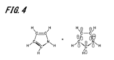
- FIG. 4 shows the structural formula and molecular orbitals of the pyrrole ring.
- the pyrrole ring has a structure in which one of the carbon atoms constituting the five-membered ring is substituted with a nitrogen atom, but the number of ⁇ electrons is also six and satisfies the Hückel rule. Nitrogen-containing aromatic ring. Since the nitrogen atom of the pyrrole ring is also bonded to a hydrogen atom, the lone pair is mobilized to the 6 ⁇ electron system.
- the nitrogen atom of the pyrrole ring has an unshared electron pair, since this unshared electron pair is used as an essential element for the expression of aromaticity, it does not participate in aromaticity and is a metal. It does not fall under [Effective unshared electron pairs] that are not coordinated to.
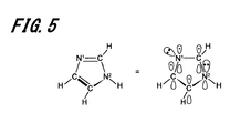
- FIG. 5 is a diagram showing the structural formula and molecular orbitals of the imidazole ring.
- the imidazole ring has a structure in which two nitrogen atoms N 1 and N 2 are substituted at the 1- and 3-positions in a 5-membered ring, and the nitrogen-containing ⁇ -electron number is also 6 It is an aromatic ring.
- one nitrogen atom N 1 is a pyridine ring-type nitrogen atom that mobilizes only one unpaired electron to the 6 ⁇ -electron system and does not utilize the unshared electron pair for the expression of aromaticity, This unshared electron pair of the nitrogen atom N 1 corresponds to [effective unshared electron pair].
- the unshared electron pair of the nitrogen atom N 2 is [effective Does not fall under [Unshared electron pair].
- FIG. 6 shows the structural formula and molecular orbital of the ⁇ -carboline ring.
- the ⁇ -carboline ring is a condensed ring compound having a nitrogen-containing aromatic ring skeleton, and is an azacarbazole compound in which a benzene ring skeleton, a pyrrole ring skeleton, and a pyridine ring skeleton are condensed in this order.
- the nitrogen atom N 3 of the pyridine ring mobilizes only one unpaired electron to the ⁇ -electron system
- the nitrogen atom N4 of the pyrrole ring mobilizes an unshared electron pair to the ⁇ -electron system, forming a ring.
- the total number of ⁇ electrons is an aromatic ring.
- the unshared electron pair of the nitrogen atom N 3 constituting the pyridine ring corresponds to [effective unshared electron pair], but constitutes a pyrrole ring.
- the unshared electron pair of the nitrogen atom constituting the condensed ring compound is involved in the bond in the condensed ring compound as well as the bond in the monocyclic compound such as pyridine ring and pyrrole ring constituting the condensed ring compound. To do.
- the [effective unshared electron pair] described above is important for expressing a strong interaction with silver which is the main component of the electrode layer 1b.
- the nitrogen atom having such an [effective unshared electron pair] is preferably a nitrogen atom in the nitrogen-containing aromatic ring from the viewpoint of stability and durability. Therefore, the compound contained in the nitrogen-containing layer 1a preferably has an aromatic heterocyclic ring in which a nitrogen atom having [effective unshared electron pair] is a heteroatom.
- the number n of [effective unshared electron pairs] with respect to the molecular weight M of such a compound is defined as, for example, the effective unshared electron pair content [n / M].
- the nitrogen-containing layer 1a is characterized in that this [n / M] is composed of a compound selected such that 2.0 ⁇ 10 ⁇ 3 ⁇ [n / M].
- the nitrogen-containing layer 1a is preferable if the effective unshared electron pair content [n / M] defined as described above is in the range of 3.9 ⁇ 10 ⁇ 3 ⁇ [n / M]. More preferably, the range is 5 ⁇ 10 ⁇ 3 ⁇ [n / M].
- the nitrogen-containing layer 1a may be configured using a compound having an effective unshared electron pair content [n / M] within the predetermined range described above, or may be configured only with such a compound. Further, such a compound and other compounds may be mixed and used. The other compound may or may not contain a nitrogen atom, and the effective unshared electron pair content [n / M] may not be within the predetermined range described above.
- the nitrogen-containing layer 1a is composed of a plurality of compounds, for example, based on the mixing ratio of the compounds, the molecular weight M of the mixed compound obtained by mixing these compounds is obtained, and [effective non- The total number n of [shared electron pairs] is obtained as an average value of the effective unshared electron pair content [n / M], and this value is preferably within the predetermined range described above. That is, it is preferable that the effective unshared electron pair content [n / M] of the nitrogen-containing layer 1a itself is within a predetermined range.
- the nitrogen-containing layer 1a is configured using a plurality of compounds and the composition ratio (content ratio) of the compounds is different in the film thickness direction, the nitrogen on the side in contact with the electrode layer 1b
- the effective unshared electron pair content [n / M] at the interface of the containing layer 1a may be within a predetermined range.
- Table 1 shows the corresponding general formulas when these exemplary compounds also belong to the general formulas (1) to (8a) representing other compounds described below.
- the compound which has a property required for every electronic device to which the transparent electrode 1 provided with this nitrogen containing layer 1a is applied is used for the other compound used for the nitrogen containing layer 1a.
- this transparent electrode 1 is used as an electrode of an organic electroluminescence device, from the viewpoint of film forming properties and electron transport properties, a compound that constitutes the nitrogen-containing layer 1a is described as a general formula (1 ) To (8a) are preferably used.
- X11 in the general formula (1) represents —N (R11) — or —O—.
- R11 and R12 each represent a hydrogen atom (H) or a substituent.
- substituents examples include an alkyl group (for example, methyl group, ethyl group, propyl group, isopropyl group, tert-butyl group, pentyl group, hexyl group, octyl group, dodecyl group, tridecyl group, tetradecyl group, pentadecyl group).
- alkyl group for example, methyl group, ethyl group, propyl group, isopropyl group, tert-butyl group, pentyl group, hexyl group, octyl group, dodecyl group, tridecyl group, tetradecyl group, pentadecyl group.
- cycloalkyl groups for example, cyclopentyl group, cyclohexyl group, etc.
- alkenyl groups for example, vinyl group, allyl group, etc.
- alkynyl groups for example, ethynyl group, propargyl group, etc.
- aromatic hydrocarbon groups aromatic Also referred to as aromatic carbocyclic group, aryl group, etc., for example, phenyl group, p-chlorophenyl group, mesityl group, tolyl group, xylyl group, naphthyl group, anthryl group, azulenyl group, acenaphthenyl group, fluorenyl group, phenanthryl group, indenyl group , Pyrenyl group, biphenylyl group), aromatic heterocyclic group (eg , Furyl group, thienyl group, pyridyl group, pyridazinyl group,
- substituents may be further substituted with the above substituents.
- a plurality of these substituents may be bonded to each other to form a ring.
- substituents those which do not inhibit the interaction between the compound and silver (Ag) are preferably used, and those having a nitrogen atom having an effective unshared electron pair described above are particularly preferably applied. .
- the above description regarding the substituents is similarly applied to the substituents shown in the description of the general formulas (2) to (8a) described below.
- a compound having the structure represented by the general formula (1) as described above is preferable because a strong interaction can be expressed between a nitrogen atom in the compound and silver constituting the electrode layer 1b.
- the compound having the structure represented by the general formula (1a) is one form of the compound having the structure represented by the general formula (1), and X11 in the general formula (1) is represented as -N (R11)-.
- a compound. Such a compound is preferable because the above interaction can be expressed more strongly.
- Such a compound is preferable because the number of nitrogen atoms is large and the above interaction can be expressed more strongly.
- the above general formula (2) is also a form of the general formula (1).
- Y21 represents a divalent linking group composed of an arylene group, a heteroarylene group, or a combination thereof.
- R21 represents a hydrogen atom (H) or a substituent.
- k21 and k22 represent an integer of 0 to 4, and k21 + k22 is an integer of 2 or more.
- examples of the arylene group represented by Y21 include o-phenylene group, p-phenylene group, naphthalenediyl group, anthracenediyl group, naphthacenediyl group, pyrenediyl group, naphthylnaphthalenediyl group, and biphenyldiyl.
- examples of the heteroarylene group represented by Y21 include a carbazole ring, a carboline ring, a diazacarbazole ring (also referred to as a monoazacarboline ring, and one of carbon atoms constituting the carboline ring is nitrogen.
- the ring structure is replaced by an atom), a triazole ring, a pyrrole ring, a pyridine ring, a pyrazine ring, a quinoxaline ring, a thiophene ring, an oxadiazole ring, a dibenzofuran ring, a dibenzothiophene ring, and an indole ring.
- a carbazole ring also referred to as a monoazacarboline ring
- a triazole ring also referred to as a monoazacarboline ring
- a pyrrole ring also referred to as a monoazacarboline ring
- a condensed aromatic heterocyclic ring formed by condensing three or more rings is used.
- a group derived from a condensed aromatic heterocyclic ring formed by condensing three or more rings is preferably included, and a group derived from a dibenzofuran ring or a dibenzothiophene ring is preferable.
- a group derived from a dibenzofuran ring or a dibenzothiophene ring is preferable.
- E221 to E224 and E230 to E233 are each represented by —C (R21) ⁇ .
- E203 is represented by —C (R21) ⁇ and R21 represents a linking site, and E211 is also —C (R21).
- R21 preferably represents a linking moiety.
- the general formula (3) is also a form of the general formula (1a-2).
- E301 to E312 each represent —C (R31) ⁇
- R31 represents a hydrogen atom (H) or a substituent.
- Y31 represents a divalent linking group composed of an arylene group, a heteroarylene group, or a combination thereof.
- the general formula (4) is also a form of the general formula (1a-1).
- E401 to E414 each represent —C (R41) ⁇
- R41 represents a hydrogen atom (H) or a substituent.
- Ar41 represents a substituted or unsubstituted aromatic hydrocarbon ring or aromatic heterocyclic ring.
- k41 represents an integer of 3 or more.
- the aromatic hydrocarbon ring includes benzene ring, biphenyl ring, naphthalene ring, azulene ring, anthracene ring, phenanthrene ring, pyrene ring, chrysene Ring, naphthacene ring, triphenylene ring, o-terphenyl ring, m-terphenyl ring, p-terphenyl ring, acenaphthene ring, coronene ring, fluorene ring, fluoranthrene ring, naphthacene ring, pentacene ring, perylene ring, pentaphen And a ring, a picene ring, a pyrene ring, a pyranthrene ring, and an anthraanthrene ring.
- These rings may further have the substituents exemplified as R11
- the aromatic heterocycle when Ar41 represents an aromatic heterocycle, the aromatic heterocycle includes a furan ring, a thiophene ring, an oxazole ring, a pyrrole ring, a pyridine ring, a pyridazine ring, a pyrimidine ring, a pyrazine ring, Triazine ring, benzimidazole ring, oxadiazole ring, triazole ring, imidazole ring, pyrazole ring, thiazole ring, indole ring, benzimidazole ring, benzothiazole ring, benzoxazole ring, quinoxaline ring, quinazoline ring, phthalazine ring, carbazole ring And azacarbazole ring.
- the azacarbazole ring refers to one in which at least one carbon atom of the benzene ring constituting the carbazole ring is replaced with a nitrogen atom. These rings may further have the substituents exemplified as R11 and R12 in the general formula (1).
- R51 represents a substituent.
- R52 represents a hydrogen atom (H) or a substituent.
- E601 to E612 each represent —C (R61) ⁇ or —N ⁇ , and R61 represents a hydrogen atom (H) or a substituent.
- Ar61 represents a substituted or unsubstituted aromatic hydrocarbon ring or aromatic heterocyclic ring.
- the substituted or unsubstituted aromatic hydrocarbon ring or aromatic heterocyclic ring represented by Ar61 may be the same as Ar41 in the general formula (4).
- R71 to R73 each represents a hydrogen atom (H) or a substituent
- Ar71 represents an aromatic hydrocarbon ring group or an aromatic heterocyclic group.
- examples of the aromatic hydrocarbon ring or aromatic heterocycle represented by Ar71 include those similar to Ar41 in the general formula (4).
- R81 to R86 each represent a hydrogen atom (H) or a substituent.
- E801 to E803 each represent —C (R87) ⁇ or —N ⁇ , and R87 represents a hydrogen atom (H) or a substituent.
- Ar81 represents an aromatic hydrocarbon ring group or an aromatic heterocyclic group.
- examples of the aromatic hydrocarbon ring or aromatic heterocycle represented by Ar81 include those similar to Ar41 in the general formula (4).
- the compound having the structure represented by the general formula (8a) is one form of the compound having the structure represented by the general formula (8), and Ar81 in the general formula (8) is a carbazole derivative.
- E804 to E811 each represent —C (R88) ⁇ or —N ⁇ , and R88 represents a hydrogen atom (H) or a substituent.
- the following compounds 1 to 166 are exemplified. Is done. These compounds are compounds containing nitrogen atoms that interact with silver constituting the electrode layer 1b. These compounds are materials having an electron transport property or an electron injection property. Therefore, the transparent electrode 1 comprising the nitrogen-containing layer 1a using these compounds is suitable as a transparent electrode in the organic electroluminescent device, and the nitrogen-containing layer 1a is used as an electron transport layer or an electron injection layer in the organic electroluminescent device. It can be used.
- these compounds 1 to 166 compounds that fall within the range of the effective unshared electron pair content [n / M] described above are also included. If such compounds are used, the nitrogen-containing layer 1a alone is formed. It can be used as a constituent compound. Further, among these compounds 1 to 166, there are compounds that fall under the general formulas (1) to (8a) described above.
- Step 1 (Synthesis of Intermediate 1) Under a nitrogen atmosphere, 2,8-dibromodibenzofuran (1.0 mol), carbazole (2.0 mol), copper powder (3.0 mol), potassium carbonate (1.5 mol), DMAc (dimethylacetamide) 300 ml Mixed in and stirred at 130 ° C. for 24 hours.
- Step 2 (Synthesis of Intermediate 2)
- Intermediate 1 (0.5 mol) was dissolved in 100 ml of DMF (dimethylformamide) at room temperature in the atmosphere, NBS (N-bromosuccinimide) (2.0 mol) was added, and the mixture was stirred overnight at room temperature. The resulting precipitate was filtered and washed with methanol, yielding intermediate 2 in 92% yield.
- Step 3 (Synthesis of Compound 5) Under a nitrogen atmosphere, intermediate 2 (0.25 mol), 2-phenylpyridine (1.0 mol), ruthenium complex [( ⁇ 6 -C 6 H 6 ) RuCl 2 ] 2 (0.05 mol), triphenyl Phosphine (0.2 mol) and potassium carbonate (12 mol) were mixed in 3 L of NMP (N-methyl-2-pyrrolidone) and stirred at 140 ° C. overnight.
- NMP N-methyl-2-pyrrolidone
- the film forming method includes a method using a wet process such as a coating method, an inkjet method, a coating method, a dip method, Examples include a method using a dry process such as a vapor deposition method (resistance heating, EB method, etc.), a sputtering method, a CVD method, or the like. Of these, the vapor deposition method is preferably applied.
- the nitrogen-containing layer 1a is formed using a plurality of compounds
- co-evaporation in which a plurality of compounds are simultaneously supplied from a plurality of evaporation sources is applied.
- a coating method is preferably applied.
- a coating solution in which the compound is dissolved in a solvent is used.
- the solvent in which the compound is dissolved is not limited.
- a coating solution may be prepared using a solvent capable of dissolving the plurality of compounds.
- the electrode layer 1b is a layer composed mainly of silver, is composed of silver or an alloy composed mainly of silver, and is a layer formed adjacent to the nitrogen-containing layer 1a.
- an alloy containing silver (Ag) as a main component constituting the electrode layer 1b is silver magnesium (AgMg), silver copper (AgCu), silver palladium (AgPd), silver palladium copper (AgPdCu), silver indium (AgIn). And silver aluminum (AgAl).
- the electrode layer 1b as described above may have a structure in which silver or an alloy layer mainly composed of silver is divided into a plurality of layers as necessary.
- the electrode layer 1b preferably has a thickness in the range of 4 to 12 nm.
- a film thickness of 12 nm or less is preferable because the absorption component or reflection component of the layer can be kept low and the light transmittance of the transparent electrode can be maintained.
- the electroconductivity of a layer is also ensured because a film thickness is 4 nm or more.
- Electrode Layer 1b As a method for forming the electrode layer 1b as described above, a wet process such as a coating method, an inkjet method, a coating method, a dip method, a vapor deposition method (resistance heating, EB method, etc.), a sputtering method, a CVD method, or the like is used. And a method using a dry process such as
- the electrode layer 1b is formed by applying the sputtering method.
- silver copper (AgCu), silver palladium (AgPd), or silver palladium copper (AgPdCu) is formed.
- the electrode layer 1b is formed by applying a sputtering method.
- the electrode layer 1b using a vapor deposition method is also formed.
- a vapor deposition method an alloy component and silver (Ag) are co-deposited.
- concentration of the alloy component with respect to silver (Ag) which is a main material by adjusting the vapor deposition rate of an alloy component and the vapor deposition rate of silver (Ag), respectively is performed.
- the electrode layer 1b is formed on the nitrogen-containing layer 1a, so that the electrode layer 1b is sufficiently conductive even without high-temperature annealing after the film formation.
- the film may be subjected to a high temperature annealing treatment after the film.
- the high refractive index layers H1 and H2 are layers having a higher refractive index than the nitrogen-containing layer 1a.
- a layer having a refractive index (n) of 2.0 or more at a wavelength of 550 nm is preferable.
- high refractive index layers H1 and H2 include high refractive index materials and materials generally used for optical films.
- high refractive index materials for example, indium oxide (In 2 O 3 ), zinc oxide (ZnO), and titanium oxide. (TiO 2 ) or an oxide containing niobium oxide (Nb 2 O 5 ) as a main component.
- Such a high refractive index material is preferable because it suppresses reflection of the transparent electrode.
- each of the high refractive index layers H1 and H2 is not used as a main electrode even when it is made of a conductive material. For this reason, each high refractive index layer H1, H2 does not need to have a film thickness required as an electrode, and the transparent electrode in an electronic device in which the transparent electrode 1 provided with these high refractive index layers H1, H2 is used. It is sufficient that the film thickness is appropriately set according to the arrangement state of 1.
- the two high refractive index layers H1 and H2 as described above may be made of the same material, or may be made of different materials. Moreover, the film thickness may be the same or different.
- examples of the film forming method include a vapor deposition method (resistance heating, EB method, etc.) or a sputtering method.
- a method using ion assist is suitable for EB deposition.
- an appropriate method is selected depending on the material constituting the layers. For example, a vapor deposition method is applied if the high refractive index layers H1 and H2 are formed using zinc oxide (ZnO) or titanium oxide (TiO 2 ).
- ZnO zinc oxide
- TiO 2 titanium oxide
- a sputtering method is applied if the high refractive index layers H1 and H2 are formed using indium oxide (In 2 O 3 ), indium tin oxide (ITO), or niobium oxide (Nb 2 O 5 ).
- the transparent electrode 1 may further have a low refractive index layer in contact with the outside of the high refractive index layers H1 and H2 for the purpose of improving light transmittance.
- a low refractive index layer is a layer having a lower refractive index than the high refractive index layers H1 and H2.
- the refractive index at a wavelength of 550 nm is preferably 0.1 or more lower than the high refractive index layers H1 and H2, and more preferably 0.3 or lower than the high refractive index layers H1 and H2.
- Such a low refractive index layer is composed of a material having a low refractive index and light transmittance.
- low refractive index materials such as magnesium fluoride (MgF 2 ), lithium fluoride (LiF), calcium fluoride (CaF 2 ), aluminum fluoride (AlF 3 ), and materials generally used for optical films. Can be mentioned.
- MgF 2 magnesium fluoride
- LiF lithium fluoride
- CaF 2 calcium fluoride
- AlF 3 aluminum fluoride
- the transparent electrode 1 as described above may be covered with a protective film or may be laminated with another conductive layer in a state where the transparent electrode 1 is sandwiched between the transparent electrode 1 and the substrate 11.
- the protective film and the conductive layer have light transmittance so as not to impair the light transmittance of the transparent electrode 1.
- the transparent electrode 1 configured as described above has a configuration in which an electrode layer 1b mainly composed of silver is provided adjacent to a nitrogen-containing layer 1a configured using a compound containing a nitrogen atom.
- an electrode layer 1b mainly composed of silver is provided adjacent to a nitrogen-containing layer 1a configured using a compound containing a nitrogen atom.
- a silver thin film that is easily isolated in an island shape by film growth of a nuclear growth type is a single layer growth type (Frank-van der Merwe: FM type) film growth.
- a film is formed. Therefore, the electrode layer 1b having a uniform film thickness can be obtained even though the film thickness is small.
- the effective unshared electron pair content [n / M] described above is applied as an index of the bond stability of silver constituting the electrode layer 1b with respect to the nitrogen-containing layer 1a, and this value is 2.0 ⁇ 10 ⁇ .
- the nitrogen-containing layer 1a By configuring the nitrogen-containing layer 1a using a compound satisfying 3 ⁇ [n / M], it is possible to provide the nitrogen-containing layer 1a that can surely obtain the effect of “suppressing the aggregation of silver” as described above. Become. This is because, as will be described later in detail, an electrode layer 1b capable of measuring sheet resistance is formed on such a nitrogen-containing layer 1a although it is an extremely thin film of 6 nm. This was also confirmed.
- the nitrogen-containing layer 1a and the electrode layer 1b are sandwiched between the high-refractive index layers H1, H2 having a higher refractive index than the nitrogen-containing layer 1a, light reflection at the transparent electrode 1 is prevented, The improvement of the light transmittance by this can also be expected.
- the material constituting the high refractive index layers H1 and H2 generally has a dense film quality, the high refractive index layer H2 having a dense film quality is disposed adjacent to the electrode layer 1b. The migration of silver (Ag) constituting the electrode layer 1b can be prevented.
- this transparent electrode 1 it is possible to reliably obtain the electrode layer 1b in which conductivity is ensured by having a uniform film thickness while ensuring light transmittance by being a thin film thickness, Furthermore, an improvement in light transmission due to prevention of light reflection can be expected. Thereby, it becomes possible to improve the reliability by maintaining the film quality of the electrode layer 1b as well as improving both the conductivity and light transmittance in the transparent electrode 1 using silver.
- Such a transparent electrode 1 is low in cost because it does not use indium (In), which is a rare metal, and has excellent long-term reliability because it does not use a chemically unstable material such as ZnO. It will be.
- the transparent electrode 1 having the above-described configuration can be used for various electronic devices.
- Examples of electronic devices include organic electroluminescent elements, LEDs (light emitting diodes), liquid crystal elements, solar cells, touch panels, etc.
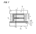
- FIG. 7 is a cross-sectional configuration diagram showing a configuration example of an organic electroluminescent element using the transparent electrode 1 described above as an example of the electronic device of the present invention. The configuration of the organic electroluminescent element will be described below based on this figure.
- the organic electroluminescent element EL shown in FIG. 7 is provided on the transparent substrate 13, and in order from the transparent substrate 13 side, the transparent electrode 1, the light emitting functional layer 3 (hole injection layer 3a / hole transport layer 3b / light emission). Layer 3c / electron transport layer 3d / electron injection layer 3e) and counter electrode 5 are laminated.
- the transparent electrode 1 is characterized in that the transparent electrode 1 of the present invention described above is used.
- the organic electroluminescent element EL according to the present embodiment is configured as a bottom emission type in which the emitted light h is extracted from at least the transparent substrate 13 side.
- the transparent electrode 1 is arranged on the anode (that is, anode) side.
- the overall layer structure of the organic electroluminescent element EL is not limited, and may be a general layer structure.
- the transparent electrode 1 may be disposed as the upper electrode on the light emitting functional layer 3, and in this case, the counter electrode 5 is disposed as the lower electrode of the light emitting functional layer 3. Further, the transparent electrode 1 may be disposed as an upper electrode and a lower electrode for the light emitting functional layer 3.
- the layer excluding the anode and the cathode is the light emitting functional layer 3 having a light emitting property.
- an anode or a cathode is comprised with either the transparent electrode 1 or the counter electrode 5 of this application.
- the light emitting functional layer 3 is a layer sandwiched between the transparent electrode 1 and the counter electrode 5, and constitutes the organic electroluminescent element EL together with the transparent electrode 1 and the counter electrode 5.
- the light emitting functional layer 3 may have a layer structure of a light emitting functional layer in a general organic electroluminescence device, and it is essential to have a light emitting layer 3c made of an organic material.
- the light emitting layer 3c is composed of a single layer or a plurality of layers.
- a non-light emitting intermediate layer may be provided between the light emitting layers.
- a hole blocking layer also referred to as a hole blocking layer
- an electron injection layer 3e also referred to as a cathode buffer layer
- An electron blocking layer also referred to as an electron barrier layer
- a hole injection layer 3a also referred to as an anode buffer layer
- the electron transport layer 3d is a layer having a function of transporting electrons, and in a broad sense, an electron injection layer and a hole blocking layer are also included in the electron transport layer 3d.
- the hole transport layer 3b is a layer having a function of transporting holes, and in a broad sense, a hole injection layer and an electron blocking layer are also included in the hole transport layer 3b. Further, the electron transport layer 3d and the hole transport layer 3b may be composed of a plurality of layers.
- the organic electroluminescent element may be an element having a so-called tandem structure in which a plurality of light emitting units including at least one light emitting layer are stacked.
- the light emitting unit is, for example, a configuration in which the anode and the cathode are excluded from the configurations (1) to (7) given in the above representative element configuration. And in the structure of the said organic electroluminescent element EL, it corresponds to the light emission functional layer 3 which has luminescent property.
- first light emitting unit, the second light emitting unit, and the third light emitting unit may all be the same or different.
- Two light emitting units may be the same, and the remaining one may be different.
- the plurality of light emitting units may be laminated directly or via an intermediate layer, and the intermediate layer is generally an intermediate electrode, an intermediate conductive layer, a charge generation layer, an electron extraction layer, a connection layer.
- a known material configuration can be used as long as it is also called an intermediate insulating layer and has a function of supplying electrons to the anode-side adjacent layer and holes to the cathode-side adjacent layer.
- Examples of materials used for the intermediate layer include ITO (indium tin oxide), IZO (indium zinc oxide), ZnO 2 , TiN, ZrN, HfN, TiOx, VOx, CuI, InN, GaN, and CuAlO 2.
- conductive inorganic compound layers Au / Bi 2 O 3, etc., two-layer films, SnO 2 / Ag / SnO 2 , ZnO / Ag / ZnO, Bi 2 O 3 / Au / Bi 2 O 3 , TiO 2 / TiN / TiO 2 , TiO 2 / ZrN / TiO 2 and other multilayer films, C60 and other fullerenes, conductive organic layers such as oligothiophene, Examples include conductive organic compound layers such as metal phthalocyanines, metal-free phthalocyanines, metal porphyrins, metal-free porphyrins, etc. Akira is not limited to these.
- Examples of a preferable configuration in the light emitting unit include the configurations (1) to (7) mentioned in the above representative element configurations, but the present invention is not limited to these.
- tandem organic electroluminescence device examples include, for example, US Pat. No. 6,337,492, US Pat. No. 7,420,203, US Pat. No. 7,473,923, and US Pat. No. 6,872. 472, U.S. Pat. No. 6,107,734, U.S. Pat. No. 6,337,492, International Publication No. 2005/009087, JP-A 2006-228712, JP-A 2006-24791, JP-A 2006-. No.
- JP-A-2007-059848, JP-A-2003-272860, JP-A-2003-045676, and International Publication No. 2005/094130 are included, but the present invention is not limited thereto. .
- the light emitting layer 3c is a layer that provides a field in which electrons and holes injected from an electrode or an adjacent layer are recombined to emit light via excitons, and the light emitting portion is within the layer of the light emitting layer 3c. Or it may be an interface between the light emitting layer 3c and the adjacent layer.
- the configuration of the light emitting layer 3c according to the present invention is not particularly limited as long as it satisfies the requirements defined in the present invention.
- the total film thickness of the light emitting layer 3c is not particularly limited, but the uniformity of the film to be formed, the application of unnecessary high voltage during light emission is prevented, and the stability of the emission color with respect to the driving current is improved. In view of the above, it is preferable to adjust to a range of 2 nm to 5 ⁇ m, more preferably to a range of 2 nm to 500 nm, and further preferably to a range of 5 nm to 200 nm.
- each light emitting layer 3c is preferably adjusted to a range of 2 nm to 1 ⁇ m, more preferably adjusted to a range of 2 nm to 200 nm, and further preferably adjusted to a range of 3 nm to 150 nm.
- the light emitting layer 3c preferably contains a light emitting dopant (a light emitting dopant compound, a dopant compound, also simply referred to as a dopant) and a host compound (a matrix material, a light emitting host compound, also simply referred to as a host).
- a light emitting dopant a light emitting dopant compound, a dopant compound, also simply referred to as a dopant
- a host compound a matrix material, a light emitting host compound, also simply referred to as a host.
- Luminescent dopant The light emitting dopant used for the light emitting layer 3c will be described.
- a fluorescent luminescent dopant also referred to as a fluorescent dopant or a fluorescent compound
- a phosphorescent dopant also referred to as a phosphorescent dopant or a phosphorescent compound
- concentration of the light emission dopant in the light emitting layer 3c it can determine arbitrarily based on the specific dopant used and the requirements of a device, and it contains with a uniform density
- a plurality of light emitting dopants may be used in combination, or a combination of dopants having different structures, or a combination of a fluorescent light emitting dopant and a phosphorescent light emitting dopant may be used. Thereby, arbitrary luminescent colors can be obtained.
- the color emitted by the organic electroluminescent element EL is shown in FIG. 4.16 on page 108 of “New Color Science Handbook” (edited by the Japan Society of Color Science, The University of Tokyo Press, 1985), with a spectral radiance meter CS-2000 (Konica Minolta). It is determined by the color when the result measured by Sensing Co., Ltd. is applied to the CIE chromaticity coordinates.
- the light emitting layer 3c of one layer or a plurality of layers contains a plurality of light emitting dopants having different emission colors and emits white light.
- the combination of the light-emitting dopants that exhibit white and examples include blue and orange, and a combination of blue, green, and red.
- the phosphorescent dopant according to the present invention is a compound in which light emission from an excited triplet is observed.
- the phosphorescent dopant is a compound that emits phosphorescence at room temperature (25 ° C.) and has a phosphorescence quantum yield of 25. Although it is defined as a compound of 0.01 or more at ° C., a preferable phosphorescence quantum yield is 0.1 or more.
- the phosphorescent quantum yield can be measured by the method described in Spectroscopic II, page 398 (1992 edition, Maruzen) of Experimental Chemistry Course 4 of the 4th edition. Although the phosphorescence quantum yield in a solution can be measured using various solvents, the phosphorescence dopant according to the present invention achieves the phosphorescence quantum yield (0.01 or more) in any solvent. That's fine.
- phosphorescent dopants There are two types of light emission of phosphorescent dopants in principle. One is the recombination of carriers on the host compound to which carriers are transported to generate an excited state of the host compound, and this energy is transferred to the phosphorescent dopant. It is an energy transfer type to obtain light emission from a phosphorescent dopant. The other is a carrier trap type in which a phosphorescent dopant serves as a carrier trap, and carrier recombination occurs on the phosphorescent dopant to emit light from the phosphorescent dopant. In any case, it is a condition that the excited state energy of the phosphorescent dopant is lower than the excited state energy of the host compound.
- the phosphorescent dopant can be appropriately selected from known ones used for the light emitting layer of the organic electroluminescent element.
- a preferable phosphorescent dopant includes an organometallic complex having Ir as a central metal. More preferably, a complex containing at least one coordination mode of a metal-carbon bond, a metal-nitrogen bond, a metal-oxygen bond, and a metal-sulfur bond is preferable.
- fluorescence dopant A fluorescence emitting dopant (hereinafter referred to as “fluorescence dopant”) will be described.
- the fluorescent dopant is a compound that can emit light from an excited singlet, and is not particularly limited as long as light emission from the excited singlet is observed.
- Examples of the fluorescent dopant include anthracene derivatives, pyrene derivatives, chrysene derivatives, fluoranthene derivatives, perylene derivatives, fluorene derivatives, arylacetylene derivatives, styrylarylene derivatives, styrylamine derivatives, arylamine derivatives, boron complexes, coumarin derivatives, pyran derivatives, Examples include cyanine derivatives, croconium derivatives, squalium derivatives, oxobenzanthracene derivatives, fluorescein derivatives, rhodamine derivatives, pyrylium derivatives, perylene derivatives, polythiophene derivatives, and rare earth complex compounds. In recent years, light emitting dopants utilizing delayed fluorescence have been developed, and these may be used.
- fluorescent dopant examples include, for example, compounds described in International Publication No. 2011/156793, Japanese Patent Application Laid-Open No. 2011-213643, Japanese Patent Application Laid-Open No. 2010-93181, etc.
- the present invention is not limited to these.
- the host compound is a compound mainly responsible for charge injection and transport in the light emitting layer 3c, and light emission of itself is not substantially observed in the organic electroluminescent element EL.
- it is a compound having a phosphorescence quantum yield of phosphorescence emission of less than 0.1 at room temperature (25 ° C.), more preferably a compound having a phosphorescence quantum yield of less than 0.01.
- the mass ratio in the layer is 20% or more among the compounds contained in the light emitting layer 3c.
- the excited state energy of the host compound is preferably higher than the excited state energy of the light-emitting dopant contained in the same layer.
- the host compounds may be used alone or in combination of two or more. By using a plurality of types of host compounds, it is possible to adjust the movement of charges, and the efficiency of the organic electroluminescent element EL can be improved.
- the compound conventionally used with an organic electroluminescent element can be used.
- it may be a low molecular compound, a high molecular compound having a repeating unit, or a compound having a reactive group such as a vinyl group or an epoxy group.
- Tg glass transition temperature
- the glass transition point (Tg) is a value determined by a method based on JIS-K-7121 using DSC (Differential Scanning Colorimetry).
- Electron transport used for the organic electroluminescent element EL is made of a material having a function of transporting electrons, and has a function of transmitting electrons injected from the cathode to the light emitting layer 3c.
- the electron transport material may be used alone or in combination of two or more.
- the total thickness of the electron transport layer 3d is not particularly limited, but is usually in the range of 2 nm to 5 ⁇ m, more preferably 2 nm to 500 nm, and further preferably 5 nm to 200 nm.
- the organic electroluminescent element EL when the light generated in the light emitting layer 3c is extracted from the electrode, the light extracted directly from the light emitting layer 3c and the light extracted after being reflected by the electrode from which the light is extracted and the counter electrode are extracted. Is known to cause interference. When light is reflected by the cathode, this interference effect can be efficiently utilized by appropriately adjusting the total film thickness of the electron transport layer 3d between several nanometers and several micrometers.
- the electron mobility of the electron transport layer 3d is 10 ⁇ 5 cm 2 / Vs or more. Is preferred.
- an electron transport material As a material used for the electron transport layer 3d (hereinafter referred to as an electron transport material), any material that has either an electron injection property or a transport property or a hole barrier property may be used. Any one can be selected and used.
- Examples include nitrogen-containing aromatic heterocyclic derivatives, aromatic hydrocarbon ring derivatives, dibenzofuran derivatives, dibenzothiophene derivatives, silole derivatives, and the like.
- nitrogen-containing aromatic heterocyclic derivatives examples include carbazole derivatives, azacarbazole derivatives (one or more carbon atoms constituting the carbazole ring are substituted with nitrogen atoms), pyridine derivatives, pyrimidine derivatives, pyrazine derivatives, pyridazine derivatives, triazine derivatives.
- aromatic hydrocarbon ring derivative examples include naphthalene derivatives, anthracene derivatives, triphenylene and the like.
- a metal complex having a quinolinol skeleton or a dibenzoquinolinol skeleton as a ligand such as tris (8-quinolinol) aluminum (Alq 3 ), tris (5,7-dichloro-8-quinolinol) aluminum, tris (5,7 -Dibromo-8-quinolinol) aluminum, tris (2-methyl-8-quinolinol) aluminum, tris (5-methyl-8-quinolinol) aluminum, bis (8-quinolinol) zinc (Znq), etc.
- a metal complex in which the central metal is replaced with In, Mg, Cu, Ca, Sn, Ga, or Pb can also be used as an electron transporting material.
- metal-free or metal phthalocyanine, or those having terminal ends substituted with an alkyl group or a sulfonic acid group can be preferably used as the electron transporting material.
- the distyrylpyrazine derivative exemplified as the material of the light emitting layer 3c can also be used as an electron transport material, and an inorganic material such as n-type Si, n-type SiC, etc. as in the case of the hole injection layer 3a and the hole transport layer 3b.
- a semiconductor can also be used as an electron transport material.
- a polymer material in which these materials are introduced into a polymer chain or these materials are used as a polymer main chain can also be used.
- the electron transport layer 3d may be doped with a doping material as a guest material to form an electron transport layer 3d having a high n property (electron rich).
- the doping material include n-type dopants such as metal complexes and metal compounds such as metal halides.
- Specific examples of the electron transport layer 3d having such a structure include, for example, JP-A-4-297076, JP-A-10-270172, JP-A-2000-196140, 2001-102175, J. Appl. Phys., 95, 5773 (2004) and the like.
- More preferable electron transport materials include pyridine derivatives, pyrimidine derivatives, pyrazine derivatives, triazine derivatives, dibenzofuran derivatives, dibenzothiophene derivatives, carbazole derivatives, azacarbazole derivatives, and benzimidazole derivatives.
- the electron transport material may be used alone or in combination of two or more.
- the hole blocking layer is a layer having the function of the electron transport layer 3d in a broad sense.
- it is made of a material having a function of transporting electrons and a small ability to transport holes. By blocking holes while transporting electrons, the recombination probability of electrons and holes can be improved.
- the structure of the above-mentioned electron transport layer 3d can be used as a hole-blocking layer as needed.
- the hole blocking layer provided in the organic electroluminescent element EL is preferably provided adjacent to the cathode side of the light emitting layer 3c.
- the thickness of the hole blocking layer is preferably in the range of 3 to 100 nm, and more preferably in the range of 5 to 30 nm.
- the material used for the hole blocking layer the material used for the above-described electron transport layer 3d is preferably used, and the material used as the above-described host compound is also preferably used for the hole blocking layer.
- the electron injection layer 3e (also referred to as “cathode buffer layer”) is a layer provided between the cathode and the light emitting layer 3c in order to lower the driving voltage and improve the light emission luminance.
- the electron injection layer 3e is “Organic EL device and its industrialization front line (November 30, 1998, issued by NTT)”, Chapter 2, Chapter 2, “Electrode material” (pages 123-166). It is described in.
- the electron injection layer 3e is provided as necessary, and is provided between the cathode and the light emitting layer 3c or between the cathode and the electron transport layer 3d as described above.
- the electron injection layer 3e is preferably a very thin film, and the film thickness is preferably in the range of 0.1 nm to 5 nm, although it depends on the material.
- membrane in which a constituent material exists intermittently may be sufficient.
- the electron injection layer 3e Details of the electron injection layer 3e are also described in JP-A-6-325871, JP-A-9-17574, JP-A-10-74586, and the like.
- Specific examples of the material preferably used for the electron injection layer 3e include metals typified by strontium and aluminum, alkali metal compounds typified by lithium fluoride, sodium fluoride, potassium fluoride, etc., magnesium fluoride, fluorine.
- alkaline earth metal compounds typified by calcium oxide, metal oxides typified by aluminum oxide, metal complexes typified by lithium 8-hydroxyquinolate (Liq), and the like.
- the material used for said electron injection layer 3e may be used independently, and may be used in combination of multiple types.
- the hole transport layer 3b is made of a material having a function of transporting holes.
- the hole transport layer 3b is a layer having a function of transmitting holes injected from the anode to the light emitting layer 3c.
- the total thickness of the hole transport layer 3b is not particularly limited, but is usually in the range of 5 nm to 5 ⁇ m, more preferably 2 nm to 500 nm, and further preferably 5 nm to 200 nm. .
- the material used for the hole transport layer 3b (hereinafter referred to as a hole transport material) only needs to have either a hole injection property or a transport property or an electron barrier property.
- a hole transport material an arbitrary material can be selected and used from conventionally known compounds.
- the hole transport material may be used alone or in combination of two or more.
- Hole transport materials include, for example, porphyrin derivatives, phthalocyanine derivatives, oxazole derivatives, oxadiazole derivatives, triazole derivatives, imidazole derivatives, pyrazoline derivatives, pyrazolone derivatives, phenylenediamine derivatives, hydrazone derivatives, stilbene derivatives, polyarylalkane derivatives, tria Reelamine derivatives, carbazole derivatives, indolocarbazole derivatives, isoindole derivatives, acene derivatives such as anthracene and naphthalene, fluorene derivatives, fluorenone derivatives, polyvinyl carbazole, polymer materials having aromatic amine introduced in the main chain or side chain, or Oligomer, polysilane, conductive polymer or oligomer (eg, PEDOT: PSS, aniline copolymer, polyaniline, polythiophene, etc.) And the like.
- PEDOT PEDOT: PS
- triarylamine derivative examples include a benzidine type typified by ⁇ -NPD, a starburst type typified by MTDATA, and a compound having fluorene or anthracene in the triarylamine linking core part.
- hexaazatriphenylene derivatives described in JP-T-2003-519432 and JP-A-2006-135145 can also be used as the hole transport material.
- a hole transport layer 3b having a high p property doped with impurities can also be used.
- the configurations described in JP-A-4-297076, JP-A-2000-196140, 2001-102175, J. Appl. Phys., 95, 5773 (2004), etc. can also be applied to the transport layer 3b.
- the above-mentioned materials can be used as the hole transport material, a triarylamine derivative, a carbazole derivative, an indolocarbazole derivative, an azatriphenylene derivative, an organometallic complex, or an aromatic amine is introduced into the main chain or side chain.
- the polymer materials or oligomers used are preferably used.
- hole transporting material used for the organic electroluminescent element EL include, but are not limited to, the compounds described in the following documents in addition to the documents listed above.
- the hole transport material may be used alone or in combination of two or more.
- the electron blocking layer is a layer having the function of the hole transport layer 3b in a broad sense. Preferably, it is made of a material having a function of transporting holes and a small ability to transport electrons.
- the electron blocking layer can improve the probability of recombination of electrons and holes by blocking electrons while transporting holes.
- the structure of the above-described hole transport layer 3b can be used as an electron blocking layer of the organic electroluminescent element EL, if necessary.
- the electron blocking layer provided in the organic electroluminescent element EL is preferably provided adjacent to the anode side of the light emitting layer 3c.
- the thickness of the electron blocking layer is preferably in the range of 3 to 100 nm, more preferably in the range of 5 to 30 nm.
- the material used for the electron blocking layer the material used for the above-described hole transport layer 3b can be preferably used. Moreover, the material used as the above-mentioned host compound can also be preferably used as the electron blocking layer.
- the hole injection layer 3a (also referred to as “anode buffer layer”) is a layer provided between the anode and the light emitting layer 3c in order to lower the driving voltage and improve the light emission luminance.
- An example of the hole injection layer 3a is “Organic EL device and its industrialization front line (issued by NTT Corporation on November 30, 1998)”, Chapter 2, Chapter 2, “Electrode materials” (pages 123-166). )It is described in.
- the hole injection layer 3a is provided as necessary, and is provided between the anode and the light emitting layer 3c or between the anode and the hole transport layer 3b as described above.
- the details of the hole injection layer 3a are also described in JP-A-9-45479, JP-A-9-260062, JP-A-8-288069, and the like.
- Examples of the material used for the hole injection layer 3a include the materials used for the hole transport layer 3b described above.
- phthalocyanine derivatives represented by copper phthalocyanine, hexaazatriphenylene derivatives as described in JP-T-2003-519432, JP-A-2006-135145, etc.
- metal oxides represented by vanadium oxide, amorphous carbon
- Conductive polymers such as polyaniline (emeraldine) and polythiophene, orthometalated complexes represented by tris (2-phenylpyridine) iridium complex, and triarylamine derivatives are preferred.
- the material used for the above-mentioned hole injection layer 3a may be used independently and may be used in combination of multiple types.
- the light emitting functional layer 3 constituting the organic electroluminescent element EL may further contain other inclusions.
- the inclusion include halogen elements such as bromine, iodine, and chlorine, halogenated compounds, alkali metals such as Pd, Ca, and Na, alkaline earth metals, transition metal compounds, complexes, and salts.
- the content of the inclusion can be arbitrarily determined, but is preferably 1000 ppm or less, more preferably 500 ppm or less, and even more preferably 50 ppm or less with respect to the total mass% of the contained layer. . However, it is not within this range depending on the purpose of improving the transportability of electrons and holes or the purpose of favoring the exciton energy transfer.
- a method for forming a light emitting functional layer (a hole injection layer, a hole transport layer, a light emitting layer, a hole blocking layer, an electron transport layer, an electron injection layer, etc.) of the organic electroluminescence element EL will be described.
- the method for forming the light emitting functional layer 3 is not particularly limited, and can be formed by a conventionally known method such as a vacuum deposition method or a wet method (wet process).
- Examples of the wet method include a spin coating method, a casting method, an ink jet method, a printing method, a die coating method, a blade coating method, a roll coating method, a spray coating method, a curtain coating method, and an LB method (Langmuir-Blodgett method).
- a method having high suitability for a roll-to-roll method such as a die coating method, a roll coating method, an ink jet method, or a spray coating method is preferable.
- liquid medium for dissolving or dispersing the material of the light emitting functional layer in the wet method examples include ketones such as methyl ethyl ketone and cyclohexanone, fatty acid esters such as ethyl acetate, halogenated hydrocarbons such as dichlorobenzene, toluene, xylene, and the like.
- Aromatic hydrocarbons such as mesitylene and cyclohexylbenzene, aliphatic hydrocarbons such as cyclohexane, decalin and dodecane, and organic solvents such as DMF and DMSO can be used.
- dispersed by a dispersion method such as ultrasonic wave, high shear force dispersion, media dispersion, or the like.
- the vapor deposition conditions vary depending on the type of compound used, etc., but generally the boat heating temperature is 50 ° C. to 450 ° C. and the degree of vacuum is 10 ⁇ 6 Pa to 10 ⁇ 10. It is desirable to select appropriately within the range of ⁇ 2 Pa, vapor deposition rate of 0.01 nm / second to 50 nm / second, substrate temperature of ⁇ 50 ° C. to 300 ° C., film thickness of 0.1 nm to 5 ⁇ m, preferably 5 nm to 200 nm.
- the organic electroluminescent element EL it is preferable to consistently produce the light emitting functional layer 3 to the counter electrode 5 by one evacuation, but it may be taken out halfway and subjected to different film forming methods. In that case, it is preferable to perform the work in a dry inert gas atmosphere. Different formation methods may be applied for each layer.
- the transparent electrode 1 is the transparent electrode 1 of FIG. 1 described above, and constitutes an anode or a cathode of the organic electroluminescent element EL.
- the high refractive index layer H2 is disposed between the light emitting functional layer 3 and the electrode layer 1b used as a substantial anode.
- the conductivity of the electrode layer 1b containing silver (Ag) as a main component is extremely high, so that the conductivity is not required for the high refractive index layer H2. Therefore, the high refractive index layers H1 and H2 may be made of a material having an appropriate refractive index from among the high refractive index materials exemplified in the transparent electrode 1 above.
- these high refractive index layers H1 and H2 do not need to have a film thickness required as an electrode, and are transparent electrodes in an electronic device in which the transparent electrode 1 including these high refractive index layers H1 and H2 is used. It is sufficient that the film thickness is appropriately set according to the arrangement state of 1.
- the transparent electrode 1 is patterned in such a shape that its terminal portion is exposed from the sealing material 17, but each of the high refractive index layers H1 and H2 and the nitrogen-containing layer 1a has good insulation. If it is a thing, it may not be patterned and only the electrode layer 1b should just be patterned.
- the counter electrode 5 is an electrode that constitutes an anode or a cathode of the organic electroluminescent element EL, and is an electrode provided on one main surface of the transparent electrode 1 via the light emitting functional layer 3.
- the counter electrode 5 is used as a cathode when the transparent electrode 1 is an anode, and as an anode when the transparent electrode 1 is a cathode, with respect to the light emitting functional layer 3 of the organic electroluminescent element EL. For this reason, at least the interface layer on the side in contact with the light emitting functional layer 3 is made of a material suitable as a cathode or an anode.
- the counter electrode 5 is configured as a reflective electrode that reflects, for example, emitted light h generated in the light emitting layer 3c of the light emitting functional layer 3 to the light extraction surface 13a side of the transparent substrate 13.
- the counter electrode 5 may be transmissive to visible light. In this case, the emitted light h can be extracted from the counter electrode 5 side.
- anode and cathode constituting the counter electrode 5 described above are as follows.
- an electrode material made of a metal, an alloy, an electrically conductive compound, and a mixture thereof having a high work function (4 eV or more, preferably 4.5 V or more) is used.
- electrode materials include metals such as Au, and conductive transparent materials such as CuI, indium tin oxide (ITO), SnO 2 , and ZnO.
- conductive transparent materials such as CuI, indium tin oxide (ITO), SnO 2 , and ZnO.
- an amorphous material such as IDIXO (In 2 O 3 —ZnO) capable of forming a transparent conductive film may be used.
- a thin film is formed by depositing these electrode materials by a method such as vapor deposition or sputtering, and a pattern having a desired shape is formed by a photolithography method.
- a method such as vapor deposition or sputtering
- a pattern having a desired shape is formed by a photolithography method.
- the pattern may be formed through a mask having a desired shape when the electrode material is formed by vapor deposition or sputtering.
- a wet film forming method such as a printing method or a coating method can also be used.
- the sheet resistance as the anode is several hundred ⁇ / sq. The following is preferred.
- the thickness of the anode depends on the material, but is usually selected in the range of 10 nm to 1 ⁇ m, preferably 10 nm to 200 nm in consideration of transparency or reflectivity.
- cathode As the cathode, an electrode substance made of a metal having a low work function (4 eV or less) (referred to as an electron injecting metal), an alloy, an electrically conductive compound, and a mixture thereof is used. Specific examples of such electrode materials include sodium, sodium-potassium alloy, magnesium, lithium, magnesium / copper mixture, magnesium / silver mixture, magnesium / aluminum mixture, magnesium / indium mixture, aluminum / aluminum oxide (Al 2 O 3 ) Mixtures, indium, lithium / aluminum mixtures, aluminum, rare earth metals and the like.
- a mixture of an electron injecting metal and a second metal having a work function value larger and more stable than that of the electron injecting metal for example, magnesium / Silver mixtures, magnesium / aluminum mixtures, magnesium / indium mixtures, aluminum / aluminum oxide (Al 2 O 3 ) mixtures, lithium / aluminum mixtures, aluminum and the like are preferred.
- the cathode can be produced by using the above electrode material by vapor deposition or sputtering.
- the sheet resistance of the cathode is several hundred ⁇ / sq. The following is preferred.
- the thickness of the cathode depends on the material, but is usually selected in the range of 10 nm to 5 ⁇ m, preferably 50 nm to 200 nm in consideration of transparency or reflectivity.
- the sealing means, protective film, protective plate, light extraction technology, and light collecting sheet applicable to the organic electroluminescent element EL will be described below in this order.
- the external extraction efficiency of light emission of the organic electroluminescent element EL at room temperature is preferably 1% or more, and more preferably 5% or more.
- the external extraction quantum efficiency (%) the number of photons emitted to the outside of the organic electroluminescence device / the number of electrons sent to the organic electroluminescence device ⁇ 100.
- a hue improvement filter such as a color filter may be used in combination, or a color conversion filter that converts the emission color from the organic electroluminescence element EL into multiple colors using a phosphor may be used in combination.
- the organic electroluminescent element EL emits light well with a small amount of power, it is weak against moisture and a non-light emitting portion is formed due to moisture absorption, so that it is preferably sealed with a sealing material 17.
- Examples of the sealing means applied to the sealing of the organic electroluminescent element EL include a method in which the sealing material 17 is bonded to the counter electrode 5 and the transparent substrate 13 with an adhesive 19.
- the sealing material 17 may be disposed so as to cover the display region of the organic electroluminescent element EL, and may be a concave plate shape or a flat plate shape. Further, the transparency and electrical insulation of the sealing material 17 are not particularly limited. However, as described above, for example, the transparent electrode 1 of the organic electroluminescent element EL is used as the upper electrode on the light emitting functional layer 3. Is made of a transparent material.
- Specific examples include a glass plate, a polymer plate / film, and a metal plate / film.
- the glass plate include soda-lime glass, barium / strontium-containing glass, lead glass, aluminosilicate glass, borosilicate glass, barium borosilicate glass, and quartz.
- the polymer plate include polycarbonate, acrylic, polyethylene terephthalate, polyether sulfide, and polysulfone.
- the metal plate include those made of one or more metals or alloys selected from the group consisting of stainless steel, iron, copper, aluminum, magnesium, nickel, zinc, chromium, titanium, molybdenum, silicon, germanium, and tantalum.
- the sealing material 17 is processed into a concave shape by sandblasting, chemical etching, or the like.
- the polymer film has an oxygen permeability measured by a method according to JIS K 7126-1987 of 1 ⁇ 10 ⁇ 3 ml / (m 2 / 24h) or less, and was measured by a method according to JIS K 7129-1992.
- water vapor permeability 25 ⁇ 0.5 ° C., relative humidity (90 ⁇ 2)%) is preferably at 1 ⁇ 10 -3 g / (m 2 / 24h) or less.
- Examples of the adhesive 19 include photocuring and thermosetting adhesives having reactive vinyl groups such as acrylic acid oligomers and methacrylic acid oligomers, and moisture curing adhesives such as 2-cyanoacrylate. Can be mentioned. Moreover, heat
- organic electroluminescent element EL may deteriorate with heat processing, what can be adhesive-hardened from room temperature to 80 degrees C or less is preferable.
- a desiccant may be dispersed in the adhesive 19.
- coating of the adhesive agent 19 to a sealing part may use a commercially available dispenser, and may print it like screen printing.
- the sealing material 17 covers the counter electrode 5 and the light emitting functional layer 3 on the counter electrode 5 on the side facing the transparent substrate 13 with the light emitting functional layer 3 interposed therebetween, and is an inorganic substance in contact with the transparent substrate 13.
- the material for forming the sealing film may be any material having a function of suppressing entry of elements such as moisture and oxygen.
- silicon oxide, silicon dioxide, silicon nitride, or the like can be used.
- the sealing film it is preferable to have a laminated structure of an inorganic layer and a layer made of an organic material, like the above-described barrier film.
- the method for forming these films is not particularly limited. For example, vacuum deposition method, sputtering method, reactive sputtering method, molecular beam epitaxy method, cluster ion beam method, ion plating method, plasma polymerization method, atmospheric pressure plasma A polymerization method, a plasma CVD method, a laser CVD method, a thermal CVD method, a coating method, or the like can be used.
- a gas phase with an inert gas such as nitrogen or argon, or a liquid phase with an inert liquid such as fluorinated hydrocarbon or silicon oil is provided. It is preferable to inject.
- the gap between the sealing material 17 and the display area of the organic electroluminescent element EL can be evacuated.
- a hygroscopic compound can be enclosed in the gap between the sealing material 17 and the display area of the organic electroluminescent element EL.
- Examples of the hygroscopic compound include metal oxides such as sodium oxide, potassium oxide, calcium oxide, barium oxide, magnesium oxide, and aluminum oxide, sulfates such as sodium sulfate, calcium sulfate, magnesium sulfate, and cobalt sulfate, calcium chloride, Metal halides such as magnesium chloride, cesium fluoride, tantalum fluoride, cerium bromide, magnesium bromide, barium iodide, magnesium iodide, barium perchlorate, and perchloric acids such as magnesium perchlorate Can be mentioned.
- Anhydrous salts are preferably used as sulfates, metal halides and perchloric acids.
- a protective film or a protective plate may be provided outside the sealing film or sealing film for sealing the organic electroluminescent element EL in order to increase the mechanical strength of the element.
- a protective film or a protective plate because the mechanical strength is not necessarily high.
- a material that can be used as the protective film or the protective plate for example, a glass plate, a polymer plate / film, a metal plate / film, or the like can be used in the same manner as the sealing material 17 described above.
- the protective film or protective plate it is preferable to use a polymer film that can be reduced in weight and thickness.
- the organic electroluminescent element EL emits light inside a layer having a higher refractive index than air (within a refractive index of about 1.6 to 2.1), and 15% to 20% of the light generated in the light emitting layer 3c. It is generally known that only a certain amount of light can be extracted. The reason for this is that light incident on the interface (for example, the interface between the transparent substrate 13 and air) at an angle ⁇ greater than the critical angle causes total reflection and is difficult to extract to the outside of the element, or the transparent substrate 13 and the transparent electrode 1. This is because the light undergoes total reflection between the transparent electrode 1 and the light emitting layer 3c, and the light is guided through the transparent electrode 1 to the light emitting layer 3c, and as a result, the light escapes in the side surface direction of the element.
- a method for improving the light extraction efficiency of the organic electroluminescence device for example, a method of forming irregularities on the surface of the transparent substrate to prevent total reflection at the interface between the transparent substrate and the air (for example, US Pat. No. 4,774,435).
- a method of improving the efficiency by giving the substrate a light condensing property for example, JP-A-63-314795
- a method of forming a reflective surface on the side surface of the element for example, JP-A-1-220394) Gazette
- a method of forming an antireflection film by introducing a flat layer having an intermediate refractive index between the substrate and the light emitter for example, Japanese Patent Application Laid-Open No.
- a substrate between the substrate and the light emitter.
- a method of introducing a flat layer having a lower refractive index than that for example, Japanese Patent Laid-Open No. 2001-202827
- a diffraction grating is provided between any of the substrate, the transparent electrode layer and the light emitting layer (including between the substrate and the outside).
- Form Law JP-A 11-283751 JP
- the organic electroluminescent element EL of the present embodiment a combination of the above methods can be used.
- a method of introducing a flat layer having a lower refractive index than that of the transparent substrate between the transparent substrate 13 and the light emitting layer 3a or a method of forming a diffraction grating between layers can be suitably used.
- the light extraction efficiency can be further improved by combining these means.
- the organic electroluminescence device EL when a medium having a low refractive index is formed between the transparent electrode 1 and the transparent substrate 13 with a thickness longer than the wavelength of light transmitted, the light emitted from the transparent electrode 1 The lower the refractive index, the higher the extraction efficiency to the outside of the element.
- the low refractive index layer formed of a low refractive index medium examples include airgel, porous silica, magnesium fluoride, and a fluorine-based polymer. Since the refractive index of the transparent substrate is generally in the range of about 1.5 to 1.7, the low refractive index layer preferably has a refractive index of about 1.5 or less. Furthermore, it is preferable that it is 1.35 or less.
- the thickness of the low refractive index layer is at least twice the wavelength of light transmitted through the medium. This is because when the thickness of the low refractive index layer is about the wavelength of light, the electromagnetic wave exuded by evanescent enters the layer adjacent to the light extraction surface side of the low refractive index layer. This is because the effect of the rate layer is reduced.
- the method of introducing a diffraction grating into an interface that causes total reflection or in any medium has a feature that the effect of improving the light extraction efficiency is high.
- This method utilizes the property that the direction of light can be changed to a specific direction different from refraction by so-called Bragg diffraction, such as first-order diffraction or second-order diffraction.
- a general one-dimensional diffraction grating having a periodic refractive index distribution only in a certain direction or a diffraction grating having a two-dimensional periodic refractive index can be applied.
- the diffraction light randomly generated in any direction is diffracted by introducing a diffraction grating having a two-dimensional periodic refractive index. Can do. For this reason, by introducing a diffraction grating having a two-dimensional periodic refractive index into the organic electroluminescence device, the refractive index distribution can be changed to a two-dimensional distribution, and light traveling in all directions is diffracted to extract light. Efficiency is improved.
- the position where the diffraction grating is introduced may be in any layer or in a medium such as the transparent substrate 13 or the transparent electrode 1, and is preferably in the vicinity of the light emitting functional layer 3 where light is generated.
- the period of the diffraction grating is preferably in the range of about 1/2 to 3 times the wavelength of light in the medium.
- the arrangement of the diffraction gratings is preferably two-dimensionally repeated, such as a square lattice, a triangular lattice, or a honeycomb lattice.
- the organic electroluminescent element EL is provided with, for example, a microlens array or a so-called condensing sheet on the light extraction surface side, thereby condensing light in a specific direction, for example, in the front direction with respect to the element light emitting surface, and thereby increasing luminance in the specific direction. Can be increased.
- a light diffusing plate / film may be used in combination with the condensing sheet.
- a diffusion film (light-up) manufactured by Kimoto Co., Ltd. can be used.
- quadrangular pyramids having a side of 30 ⁇ m and an apex angle of 90 degrees are arranged two-dimensionally on the light extraction surface side of the substrate.
- One side is preferably within a range of 10 to 100 ⁇ m. If it becomes smaller than this, the effect of diffraction will generate
- the condensing sheet for example, a sheet that has been put to practical use in an LED backlight of a liquid crystal display device can be used.
- a sheet for example, a brightness enhancement film (BEF) manufactured by Sumitomo 3M Limited can be used.
- BEF brightness enhancement film
- a prism sheet for example, a shape in which a stripe having a triangular cross section with a vertex angle of 90 degrees and a pitch of 50 ⁇ m is formed on a base material, a shape in which the vertex angle is rounded, a shape in which the pitch is randomly changed, and other Shapes can be used.
- the organic electroluminescent element EL can be applied to electronic devices such as display devices, displays, and various light emission sources.
- Examples of light-emitting light sources include lighting devices such as home lighting and interior lighting, backlights for clocks and liquid crystals, signboard advertisements, traffic lights, optical storage media and other light sources, light sources for electrophotographic copying machines, and light sources for optical communication processors. Examples include, but are not limited to, a light source of an optical sensor. In particular, it can be effectively used as a backlight of a liquid crystal display device and an illumination light source.
- patterning may be performed by a metal mask, an ink jet printing method, or the like as needed during film formation.
- a metal mask an ink jet printing method, or the like as needed during film formation.
- the transparent electrode 1 and the counter electrode 5 may be patterned, these electrodes and the light emitting layer 3c may be patterned, or the whole element layer may be patterned.
- a conventionally known method can be used.
- the organic electroluminescent element used in the illumination device may be designed such that the organic electroluminescent element EL having the above-described configuration has a resonator structure.
- Examples of the purpose of use of the organic electroluminescence device configured as a resonator structure include, but are not limited to, a light source of an optical storage medium, a light source of an electrophotographic copying machine, a light source of an optical communication processor, a light source of an optical sensor, and the like. Not. Moreover, you may use for the said use by making a laser oscillation.
- the material used for the organic electroluminescent element can be applied to an organic electroluminescent element that generates substantially white light emission (also referred to as a white organic electroluminescent element).
- a plurality of light emitting materials can simultaneously emit a plurality of light emission colors to obtain white light emission by color mixing.
- the combination of a plurality of emission colors may include three emission maximum wavelengths of the three primary colors of red, green and blue, or two using the complementary colors such as blue and yellow, blue green and orange. The thing containing the light emission maximum wavelength may be used.
- the combination of luminescent materials for obtaining multiple luminescent colors is a combination of multiple phosphorescent or fluorescent materials that emit light, fluorescent materials or phosphorescent materials, and light from the luminescent materials. Any combination with a dye material that emits light as light may be used, but in a white organic electroluminescent element, a combination of a plurality of light-emitting dopants may be used.
- Such a white organic EL element is different from a configuration in which organic EL elements emitting each color are individually arranged in parallel to obtain white light emission, and the organic EL element itself emits white light. For this reason, a mask is not required for film formation of most layers constituting the element, and for example, an electrode film can be formed on one side by vapor deposition, casting, spin coating, ink jet, printing, etc., and productivity is improved. To do.
- the light emitting material used for the light emitting layer of such a white organic electroluminescent element is not particularly limited.
- a backlight in a liquid crystal display element is adapted to a wavelength range corresponding to the CF (color filter) characteristics.
- any metal complex according to the present invention or a known light emitting material may be selected and combined to be whitened.
- the white organic electroluminescent element described above it is possible to produce a lighting device that emits substantially white light.
- the lighting device can also be used as a lighting device having a large light emitting surface by using, for example, a plurality of organic electroluminescent elements.
- the light emitting surface is enlarged by arranging a plurality of light emitting panels provided with organic electroluminescent elements on the support substrate (that is, tiling).
- the support substrate may also serve as a sealing material, and each light emitting panel is tiled in a state where the organic electroluminescent element is sandwiched between the support substrate and the transparent substrate of the light emitting panel.
- An adhesive may be filled between the support substrate and the transparent substrate, thereby sealing the organic electroluminescent element. Note that the terminals of the transparent electrode and the counter electrode are exposed around the light emitting panel.
- the center of each light emitting panel is a light emitting region, and a non-light emitting region is generated between the light emitting panels.
- a light extraction member for increasing the amount of light extracted from the non-light emitting area may be provided in the non-light emitting area of the light extraction surface.
- a light collecting sheet or a light diffusion sheet can be used as the light extraction member.
- the organic electroluminescent element EL described above uses the transparent electrode 1 having both conductivity and light transmittance of the present invention and improved reliability as an anode, and the high refractive index layer H2 side of the transparent electrode 1 is used. Further, the light emitting functional layer 3 and the counter electrode 5 serving as the cathode are provided in this order. For this reason, a sufficient voltage is applied between the transparent electrode 1 and the counter electrode 5 to realize high-luminance light emission in the organic electroluminescent element EL, and the extraction efficiency of the emitted light h from the transparent electrode 1 side is improved. By doing so, it is possible to increase the brightness. Moreover, such performance can be maintained for a long time, and long-term reliability can be improved. Further, the light emission life can be improved by reducing the driving voltage for obtaining the predetermined luminance.
- a transparent non-alkali glass base material was fixed to a base material holder of a commercially available vacuum vapor deposition apparatus and attached in a vacuum chamber of the vacuum vapor deposition apparatus.
- silver (Ag) was put into the resistance heating boat made from tungsten, and it attached in the said vacuum chamber.
- the resistance heating boat was energized and heated, and the electrode layers made of silver were respectively deposited at a deposition rate of 0.1 nm / second to 0.2 nm / second. It was formed with a film thickness.
- an electrode layer was formed with a thickness of 6 nm
- Sample 102 an electrode layer was formed with a thickness of 15 nm.
- a high refractive index layer was formed on a transparent alkali-free glass substrate.
- a high refractive index layer made of titanium oxide (TiO 2 ) was formed using an electron beam evaporation apparatus.
- a copper (Cu) hearth liner containing titanium oxide (TiO 2 ) was set in the vacuum chamber of the electron beam evaporation apparatus, and oxygen gas (O 2 ) was added to the vacuum chamber to 2 ⁇
- the pressure was reduced to 10 ⁇ 2 Pa, and a high refractive index layer having a film thickness of 40 nm was formed at a film formation rate of 0.2 nm / second using ion-assisted deposition (IAD).
- IAD ion-assisted deposition
- a high refractive index layer composed of niobium oxide (Nb 2 O 5 ) was formed using a sputter deposition apparatus.
- a high refractive index layer having a film thickness of 40 nm was formed at a film forming speed of 0.2 nm / sec with an RF (high frequency) bias of 300 W in a sputtering film forming apparatus.
- the base material formed up to the high refractive index layer was transferred to the vacuum tank of the vacuum deposition apparatus while maintaining the vacuum state in each film forming apparatus, and the vacuum tank was depressurized to 4 ⁇ 10 ⁇ 4 Pa, The heating boat containing silver was energized and heated. Thereby, an electrode layer made of silver having a film thickness of 9 nm was formed at a deposition rate of 0.1 nm / second.
- a high refractive index layer was formed on the electrode layer in the same procedure as described above. That is, in the sample 103, a high refractive index layer made of titanium oxide (TiO 2 ) was formed with a film thickness of 40 nm by ion-assisted vapor deposition (IAD) using an electron beam vapor deposition apparatus. In the sample 104, a high refractive index layer made of niobium oxide (Nb 2 O 5 ) was formed with a film thickness of 40 nm using a sputtering film forming apparatus. At this time, the base material formed up to the electrode layer was moved to each film forming apparatus while maintaining the vacuum state in the vacuum chamber of the vacuum vapor deposition apparatus to form a high refractive index layer.
- IAD ion-assisted vapor deposition
- the transparent electrodes of Samples 103 and 104 in which the high refractive index layer, the electrode layer using silver, and the high refractive index layer were laminated in this order were produced.
- a transparent alkali-free glass substrate was fixed to a substrate holder of a commercially available vacuum deposition apparatus.
- silver (Ag) and aluminum (Al) were put in a resistance heating boat made of tungsten, respectively, and these substrate holder and resistance heating boat were attached to a vacuum chamber of a vacuum deposition apparatus.
- 20.0 atomic% of aluminum (Al) was added to silver (Ag) by co-evaporation with the deposition rate adjusted by adjusting the current to each resistance heating boat.
- An electrode layer added and alloyed at a concentration of 5 nm was formed to a thickness of 9 nm.
- a transparent electrode having a two-layer structure including a nitrogen-containing layer containing nitrogen and an electrode layer made of silver using each material shown in Table 2 below was formed on a glass substrate.
- an underlayer containing no nitrogen was formed instead of the nitrogen-containing layer.
- a transparent alkali-free glass substrate was fixed to a substrate holder of a commercially available vacuum deposition apparatus.
- each compound shown in following Table 2 was put into the resistance heating boat made from a tantalum.
- These substrate holders and resistance heating boats were attached to the first vacuum chamber of the vacuum deposition apparatus.
- silver (Ag) was put into the resistance heating boat made from tungsten, and it attached in the 2nd vacuum chamber of a vacuum evaporation system.
- the compound (1) is anthracene containing no nitrogen atom, and the compound (2) contains nitrogen but has an effective unshared electron pair content [n / M] value of [n / M]. n / M] ⁇ 2.0 ⁇ 10 ⁇ 3 .
- the value of the effective unshared electron pair content [n / M] appropriately selected from the compounds shown in Table 1 is 2.0 ⁇ 10 ⁇ 3 ⁇ [n / M].
- Table 2 below also shows the number of effective unshared electron pairs [n], molecular weight [M], and effective unshared electron pair content [n / M] of the compounds used here.
- the heating boat containing each compound was energized and heated, and deposited on the substrate at a deposition rate of 0.1 nm / sec to 0.2 nm / sec.
- a nitrogen-containing layer composed of each compound having a thickness of 3 nm was provided.
- the base material formed up to the nitrogen-containing layer is transferred to the second vacuum chamber while maintaining a vacuum, and after the pressure in the second vacuum chamber is reduced to 4 ⁇ 10 ⁇ 4 Pa, the heating boat containing silver is energized and heated. did.
- an electrode layer made of silver having a film thickness of 9 nm was formed at a deposition rate of 0.1 nm / second to 0.2 nm / second, and samples 106 to 109 having a laminated structure of a nitrogen-containing layer and the upper electrode layer were formed. Each transparent electrode was obtained.
- a high refractive index layer having a thickness of 40 nm was formed on a transparent alkali-free glass substrate.
- film formation using different film forming apparatuses was performed depending on the material constituting the high refractive index layer. That is, a high-refractive index layer composed of niobium oxide (Nb 2 O 5 ), indium zinc oxide (IZO), or indium tin oxide (ITO) was formed using a sputtering film forming apparatus.
- a high-refractive index layer composed of niobium oxide (Nb 2 O 5 ), indium zinc oxide (IZO), or indium tin oxide (ITO) was formed using a sputtering film forming apparatus.
- a high refractive index layer composed of titanium oxide (TiO 2 ) film formation was performed by ion-assisted vapor deposition (IAD) using an electron beam vapor deposition apparatus. Formation of the high refractive index layer using each of these apparatuses was performed in the same
- each compound shown in Table 2 was placed in a resistance heating boat made of tantalum and attached in the first vacuum chamber of the vacuum evaporation apparatus. Moreover, silver (Ag) was put into the resistance heating boat made from tungsten, and it attached in the 2nd vacuum chamber of a vacuum evaporation system. In Sample 116, silver (Ag) and aluminum (Al) were put in each resistance heating boat made of tungsten.
- the base material on which the layers up to the high refractive index layer were formed was transferred to the first vacuum chamber of the vacuum evaporation apparatus while maintaining the vacuum state in each film forming apparatus, and the first vacuum tank was 4 ⁇ 10 ⁇ 4 Pa.
- a heating boat containing each compound is energized and heated to form a nitrogen-containing layer composed of each compound with a film thickness of 3 nm on the substrate at a deposition rate of 0.1 nm / sec to 0.2 nm / sec. did.
- the base material formed up to the nitrogen-containing layer is transferred to the second vacuum chamber while maintaining a vacuum, and after the pressure in the second vacuum chamber is reduced to 4 ⁇ 10 ⁇ 4 Pa, the deposition rate is adjusted by adjusting the current to the resistance heating boat.
- An electrode layer made of silver (Ag) was formed with a film thickness of 9 nm by the adjusted vapor deposition.
- an electrode layer formed by alloying by adding silver (Ag) and aluminum (Al) at a concentration of 20.0 atomic% was formed with a film thickness of 9 nm by co-evaporation with the deposition rate adjusted.
- a high refractive index layer having a thickness of 40 nm was formed on the electrode layer in the same procedure as described above. That is, a high-refractive index layer made of niobium oxide (Nb 2 O 5 ), indium zinc oxide (IZO), or indium tin oxide (ITO) was formed using a sputtering film forming apparatus. On the other hand, for the formation of the high refractive index layer composed of titanium oxide (TiO 2 ), film formation was performed by ion-assisted vapor deposition (IAD) using an electron beam vapor deposition apparatus. Formation of the high refractive index layer using each of these apparatuses was performed in the same manner as described in the samples 103 and 104.
- IAD ion-assisted vapor deposition
- the base material formed up to the electrode layer was moved to each film forming apparatus while maintaining the vacuum state in the vacuum chamber of the vacuum vapor deposition apparatus to form a high refractive index layer.
- the transparent electrodes of Samples 110 to 135 in which the high refractive index layer, the nitrogen-containing layer, the electrode layer, and the high refractive index layer were laminated in this order were produced.
- each of the samples 136 and 137 is transparent in the same procedure as the samples 122 and 129 except that the base material is formed using a polyethylene terephthalate (PET) base material. An electrode was produced.
- PET polyethylene terephthalate
- Example 1 As is apparent from Table 2, the transparent electrodes of Samples 110 to 137, that is, the high refractive index layer, the nitrogen-containing layer, the electrode layer mainly composed of silver (Ag), and the high refractive index layer were laminated in this order.
- the transparent electrode has a sheet resistance value of 10 ⁇ / sq.
- the high-temperature and high-humidity storage stability is 140% or less, and it has been confirmed that this is a transparent electrode that achieves both improvement in conductivity and improvement in light transmission, as well as improvement in reliability.
- a nitrogen-containing layer constituted by using a compound having an effective unshared electron pair content [n / M] of 2.0 ⁇ 10 ⁇ 3 ⁇ [n / M].
- the provided transparent electrodes 110 to 113, 115 and 117 to 137 have a lower sheet resistance and a single-layer growth type (Frank-van der Merwe: FM type) compared to the transparent electrode (Sample 114) not provided with the transparent electrodes. It was confirmed that the film was formed with a substantially uniform film thickness by the film growth.
- the transparent electrodes of Sample 105 and Sample 116 that is, transparent electrodes having electrode layers alloyed with silver (Ag) and aluminum (Al) are compared, the effective unshared electron pair content [n / M]
- the transparent electrode 116 having a nitrogen-containing layer formed using a compound having a ratio of 2.0 ⁇ 10 ⁇ 3 ⁇ [n / M] has a lower sheet resistance than the transparent electrode 105 not having the nitrogen-containing layer. It was confirmed that the film was formed with a substantially uniform film thickness by single-layer growth type (Frank-van der Merwe: FM type) film growth.
- the transparent electrodes of these samples 110 to 113 and 115 to 137 had a high temperature / high humidity storage stability of 100% and were excellent in high temperature / high humidity resistance.
- the sample 101 without a base layer such as a nitrogen-containing layer cannot measure the sheet resistance, and the sample 102 has a film thickness of 15 nm as the electrode layer. The rate was low and it could not be used as a transparent electrode.
- a transparent electrode that is improved in reliability as well as improved in conductivity and light transmittance is It was not obtained.
- the transparent electrode of Sample 134 is formed by using a No. 47 compound having a nitro group to form a nitrogen-containing layer, and has good results in light transmittance, sheet resistance, and high temperature / high humidity storage stability. It was confirmed that In addition, even when compared with the sample 133 configured using No. 46 having an effective unshared electron pair content [n / M] substantially equal to that of the sample 134, the same good results were obtained. Therefore, the unshared electron pair possessed by the nitrogen atom of the nitro group (—NO 2 ) is used for the resonance structure with the oxygen atom, but does not participate in aromaticity and is not coordinated to the metal. It was confirmed that the electron pair was effective as a [effective unshared electron pair] for bonding with silver (Ag).
- FIG. 8 shows compounds No. 1 to No. in which the effective unshared electron pair content [n / M] is 2.0 ⁇ 10 ⁇ 3 ⁇ [n / M] ⁇ 1.9 ⁇ 10 ⁇ 2.
- the effective unshared electron pair content of the compound constituting the nitrogen-containing layer [n / M ] is shown.
- a thin film is obtained in order to obtain light transmissivity by selecting and using a compound constituting the nitrogen-containing layer provided adjacent to the electrode layer using the effective unshared electron pair content [n / M] as an index.
- an electrode film having low resistance that is, a transparent electrode
- a hole transport / injection layer that serves both as a hole injection layer and a hole transport layer made of ⁇ -NPD, heated by energizing a heating boat containing ⁇ -NPD represented by the following structural formula as a hole transport injection material 31 was formed on the transparent electrode 1 ′.
- the deposition rate was 0.1 nm / second to 0.2 nm / second, and the film thickness was 20 nm.
- a heating boat containing the host material H-1 represented by the following structural formula and a heating boat containing the phosphorescent compound Ir1 represented by the following structural formula were respectively energized independently, and the host material H-1 and A light emitting layer 32 made of the phosphorescent compound Ir1 was formed on the hole transport / injection layer 31.
- the film thickness was 30 nm.
- a heating boat containing BAlq represented by the following structural formula as a hole blocking material was energized and heated to form a hole blocking layer 33 made of BAlq on the light emitting layer 32.
- the deposition rate was 0.1 nm / second to 0.2 nm / second, and the film thickness was 10 nm.
- the transparent substrate 13 on which the light emitting functional layer 3 is formed is transferred into the second vacuum chamber of the vacuum deposition apparatus, and the second vacuum chamber is depressurized to 4 ⁇ 10 ⁇ 4 Pa.
- the heating boat containing aluminum attached in the vacuum chamber was energized and heated.
- the counter electrode 5 made of aluminum having a film thickness of 100 nm was formed at a deposition rate of 0.3 nm / second.
- the counter electrode 5 is used as a cathode.
- a bottom emission type organic electroluminescent element EL was formed on the transparent substrate 13.
- the organic electroluminescent element EL is covered with a sealing material 17 made of a glass substrate having a thickness of 300 ⁇ m, and the adhesive 19 (between the sealing material 17 and the transparent substrate 13 is surrounded by the organic electroluminescent element EL. Sealing material) was filled.
- a sealing material 17 made of a glass substrate having a thickness of 300 ⁇ m As the adhesive 19, an epoxy photocurable adhesive (Lux Track LC0629B manufactured by Toagosei Co., Ltd.) was used.
- the adhesive 19 filled between the sealing material 17 and the transparent substrate 13 is irradiated with UV light from the side of the sealing material 17 made of a glass substrate, and the adhesive 19 is cured, whereby the organic electroluminescent element EL is formed. Sealed.
- the organic electroluminescent element EL In the formation of the organic electroluminescent element EL, a vapor deposition mask is used for forming each layer, and the central 4.5 cm ⁇ 4.5 cm of the 5 cm ⁇ 5 cm transparent substrate 13 is defined as the light emitting region A, and the entire light emitting region A is formed.
- a non-light emitting region B having a width of 0.25 cm was provided on the periphery.
- the electrode layer 1 b of the transparent electrode 1 ′ serving as the anode and the counter electrode 5 serving as the cathode are insulated by the hole transport / injection layer 31 to the electron transport / injection layer 34, and the peripheral edge of the transparent substrate 13. The terminal part was formed in the shape pulled out.
- the organic electroluminescent elements EL were provided on the transparent substrate 13, and the light emitting panels of the organic electroluminescent elements of Samples 201 to 229 in which the organic electroluminescent elements EL were sealed with the sealing material 17 and the adhesive 19 were obtained. . In each of these light emitting panels, each color of emitted light h generated in the light emitting layer 32 is extracted from the transparent substrate 13 side.
- External quantum efficiency is measured by using a spectral radiance meter CS-1000 (manufactured by Konica Minolta Sensing Co., Ltd.) to measure the luminance and emission spectrum when each organic electroluminescent device emits light. Based on the measured value, it was calculated by the luminance conversion method.
- the value of the organic electroluminescent element of the sample 201 is shown as a relative value with 1.0.
- the number of luminescence (n / 10) is the number of luminescence confirmed even after storage for 300 hours among the ten samples 201 to 229, and is preferably closer to 10.
- the amount of change ⁇ V in the drive voltage is calculated as an average value of the organic electroluminescent elements EL in which light emission was confirmed after storage in each of the samples 201 to 229, and the smaller the value, the better.
- Rectification ratio [log] is the current value when + 2.5V drive voltage is applied in the forward direction and -2.5V drive voltage is applied in the reverse direction to each light-emitting panel after storage.
- each of the organic electroluminescent elements EL of Samples 208 to 229 that is, a high refractive index layer, a nitrogen-containing layer, an electrode layer containing silver (Ag) as a main component and an additive element, and a high refractive index
- the organic electroluminescent element EL using the transparent electrode in which the layers are laminated in this order has a higher external quantum efficiency (EQE) and excellent emission characteristics compared with the samples 201 to 207, and after storage in a high temperature and high humidity environment.
- the drive voltage difference is low, light emission is confirmed after storage in all 10 samples, and the rectification ratio [log] after storage is sufficient and leakage is suppressed. It was confirmed to be excellent.
- the electroluminescent device EL has a high external quantum efficiency (EQE) of 1.19 or higher, a drive voltage difference after storage at high temperature and high humidity is suppressed to 1.2 or lower, and a rectification ratio of 4.0 or higher is high. High humidity resistance was also good.
- the organic electroluminescent element EL using the transparent electrode 1 ′ having the configuration of the present invention can emit light with high luminance at a low driving voltage and has excellent long-term reliability. Furthermore, it was confirmed that the drive voltage for obtaining the predetermined luminance is reduced and the light emission life is expected to be improved.
- the transparent electrodes of samples 208 to 229 having the structure of the present invention produced in Example 1 were formed as anodes on a glass transparent substrate having a size of 30 mm ⁇ 30 mm and a thickness of 0.7 mm.
- the transparent substrate on which each anode was formed was fixed to a substrate holder of a commercially available vacuum deposition apparatus.
- each of crucibles for vapor deposition in the vacuum vapor deposition apparatus was filled with the constituent material of each layer to be formed next in an optimum amount for device fabrication, and fixed to the vacuum vapor deposition apparatus.
- the evaporation crucible used was made of a resistance heating material made of molybdenum or tungsten.
- the inside of the vacuum deposition apparatus is depressurized to a vacuum of 1 ⁇ 10 ⁇ 4 Pa, and then the deposition crucible containing ⁇ -NPD is energized and heated to deposit on the transparent electrode at a deposition rate of 0.1 nm / second. Then, a hole injecting and transporting layer having a thickness of 40 nm was formed.
- the following compound BD-1 which is a blue light-emitting dopant and the following compound H-2 which is a host compound are co-deposited at a deposition rate of 0.1 nm / second so that the compound BD-1 has a concentration of 5%.
- a fluorescent light emitting layer exhibiting blue light emission with a film thickness of 15 nm was formed.
- the following compound GD-1 which is a green luminescent dopant
- the following compound RD-1 which is a red luminescent dopant
- the following compound H-3 which is a host compound
- compound GD-1 is Compound D-15 previously shown as the luminescent dopant
- Compound RD-1 is Compound D-1 previously shown as the luminescent dopant.
- Compound E-1 was deposited at a deposition rate of 0.1 nm / second to form an electron transport layer having a thickness of 30 nm.
- Compound E-1 is Compound 10 shown above as a material constituting the nitrogen-containing layer.
- the transparent electrodes of samples 208 to 229 having the structure of the present invention produced in Example 1 were formed as anodes on a glass transparent substrate having a size of 30 mm ⁇ 30 mm and a thickness of 0.7 mm.
- the transparent substrate on which each anode was formed was fixed to a substrate holder of a commercially available vacuum deposition apparatus.
- each of crucibles for vapor deposition in the vacuum vapor deposition apparatus was filled with the constituent material of each layer to be formed next in an optimum amount for device fabrication, and fixed to the vacuum vapor deposition apparatus.
- the evaporation crucible used was made of a resistance heating material made of molybdenum or tungsten.
- the inside of the vacuum deposition apparatus is depressurized to a vacuum of 1 ⁇ 10 ⁇ 4 Pa, and then the deposition crucible containing ⁇ -NPD is energized and heated to deposit on the transparent electrode at a deposition rate of 0.1 nm / second. Then, a hole injecting and transporting layer having a thickness of 40 nm was formed.
- the compound BD-1 which is a blue light-emitting dopant and the compound H-2 which is a host compound are co-deposited at a deposition rate of 0.1 nm / second so that the compound BD-1 has a concentration of 5%.
- a fluorescent light emitting layer exhibiting blue light emission with a film thickness of 30 nm was formed.
- the compound E-1 was deposited at a deposition rate of 0.1 nm / second to form an electron transport layer having a thickness of 30 nm.
- lithium was deposited to a thickness of 1 nm to form an intermediate metal layer.
- the ⁇ -NPD was deposited at a deposition rate of 0.1 nm / second to form a 50 nm-thick hole injecting and transporting layer.
- the compound GD-1 which is a green light-emitting dopant
- the compound RD-1 which is a red light-emitting dopant
- the compound H-3 which is a host compound
- the compound E-1 was deposited at a deposition rate of 0.1 nm / second to form an electron transport layer having a thickness of 30 nm.
Landscapes
- Physics & Mathematics (AREA)
- Chemical & Material Sciences (AREA)
- Engineering & Computer Science (AREA)
- Materials Engineering (AREA)
- Spectroscopy & Molecular Physics (AREA)
- Optics & Photonics (AREA)
- Electroluminescent Light Sources (AREA)
- Laminated Bodies (AREA)
Abstract
Description
1.透明電極
2.透明電極の用途
3.有機電界発光素子
4.照明装置
図1は、本発明の実施形態の透明電極の構成を示す断面模式図である。この図に示すように、透明電極1は、窒素含有層1aと、これに隣接して設けられた電極層1bと、これらを挟持する2層の高屈折率層H1,H2とを積層した4層構造であり、例えば基材11の上部に、高屈折率層H1、窒素含有層1a、電極層1b、高屈折率層H2の順に設けられている。このうち、透明電極1における電極部分を構成する電極層1bは、銀(Ag)を主成分として構成された層である。また電極層1bに対する窒素含有層1aは、窒素原子(N)を含有する化合物を用いて構成されており、特に電極層1bを構成する主材料である銀と安定的に結合する窒素原子の非共有電子対を[有効非共有電子対]とし、この[有効非共有電子対]の含有率が所定範囲である化合物を用いていることを特徴としている。また高屈折率層H1,H2は、窒素含有層1aよりも屈折率が高い層である。
本発明の透明電極1が形成される基材11は、例えばガラス、プラスチック等を挙げることができるが、これらに限定されない。また、基材11は透明であっても不透明であってもよい。本発明の透明電極1が、基材11側から光を取り出す電子デバイスに用いられる場合には、基材11は透明であることが好ましい。好ましく用いられる透明な基材11としては、ガラス、石英、透明樹脂フィルムを挙げることができる。
窒素含有層1aは、電極層1bに隣接して設けられた層であり、窒素原子(N)を含有する化合物を用いて構成されている。窒素含有層1aの膜厚は、1μm以下、好ましくは100nm以下である。そして特にこの化合物は、一例として当該化合物に含有される窒素原子のうち、特に電極層1bを構成する主材料である銀と安定的に結合する窒素原子の非共有電子対を[有効非共有電子対]とし、この[有効非共有電子対]の含有率が所定範囲であることを特徴としている。
以下に、窒素含有層1aを構成する化合物として、上述した有効非共有電子対含有率[n/M]が2.0×10-3≦[n/M]を満たす化合物の具体例(No.1~No.48)を示す。各化合物No.1~No.48には、[有効非共有電子対]を有する窒素原子に対して○を付した。また、下記表1には、これらの化合物No.1~No.48の分子量M、[有効非共有電子対]の数n、および有効非共有電子対含有率[n/M]を示す。下記化合物33の銅フタロシアニンにおいては、窒素原子が有する非共有電子対のうち銅に配位していない非共有電子対が[有効非共有電子対]としてカウントされる。

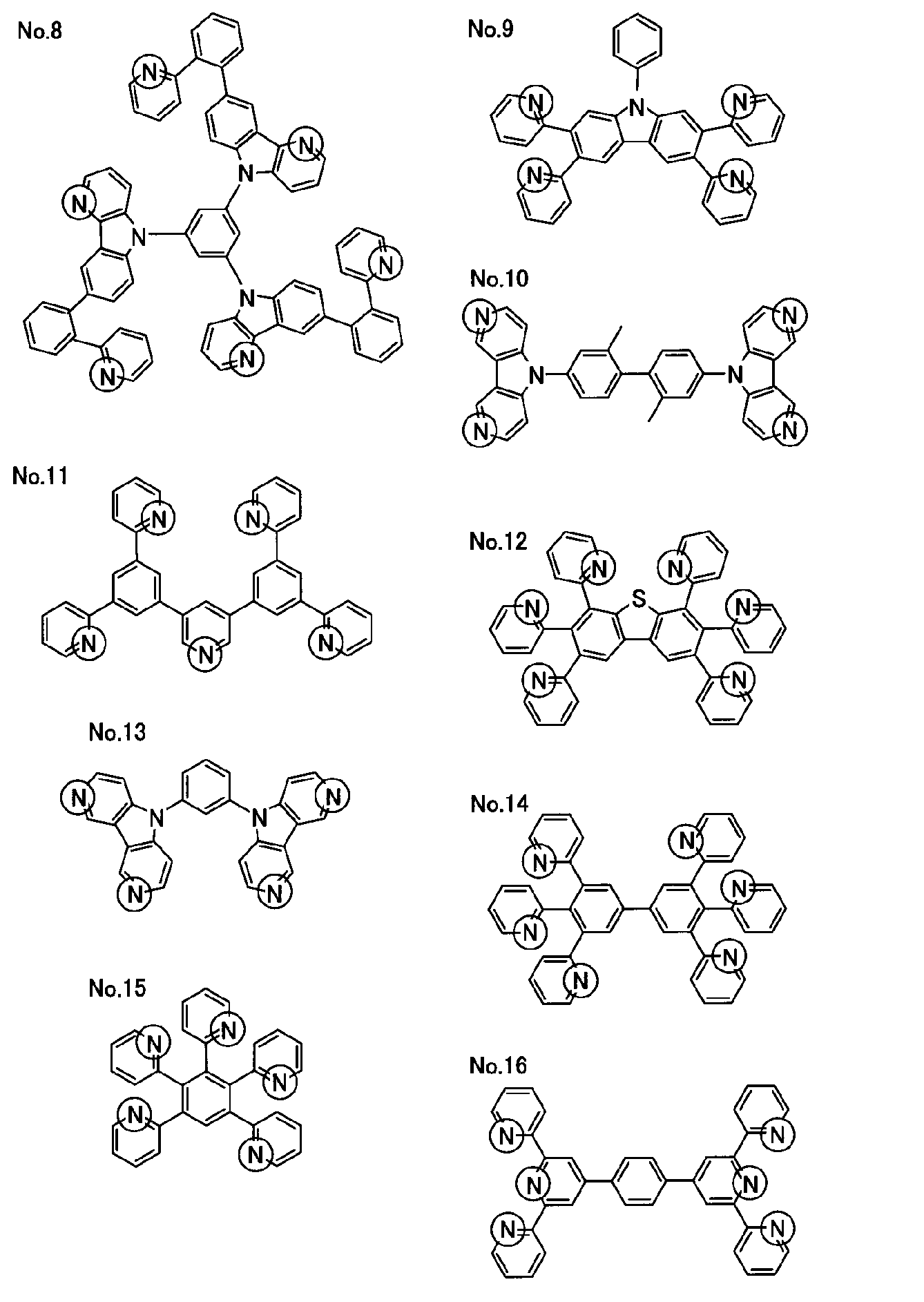

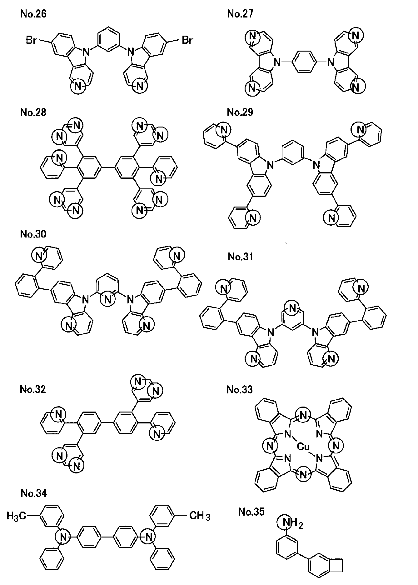
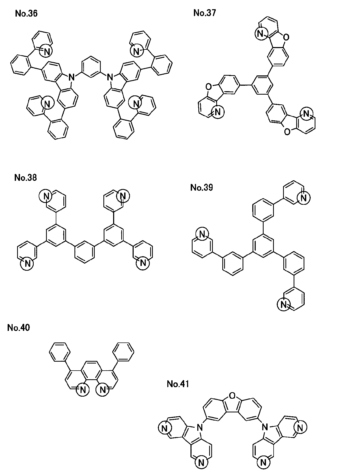

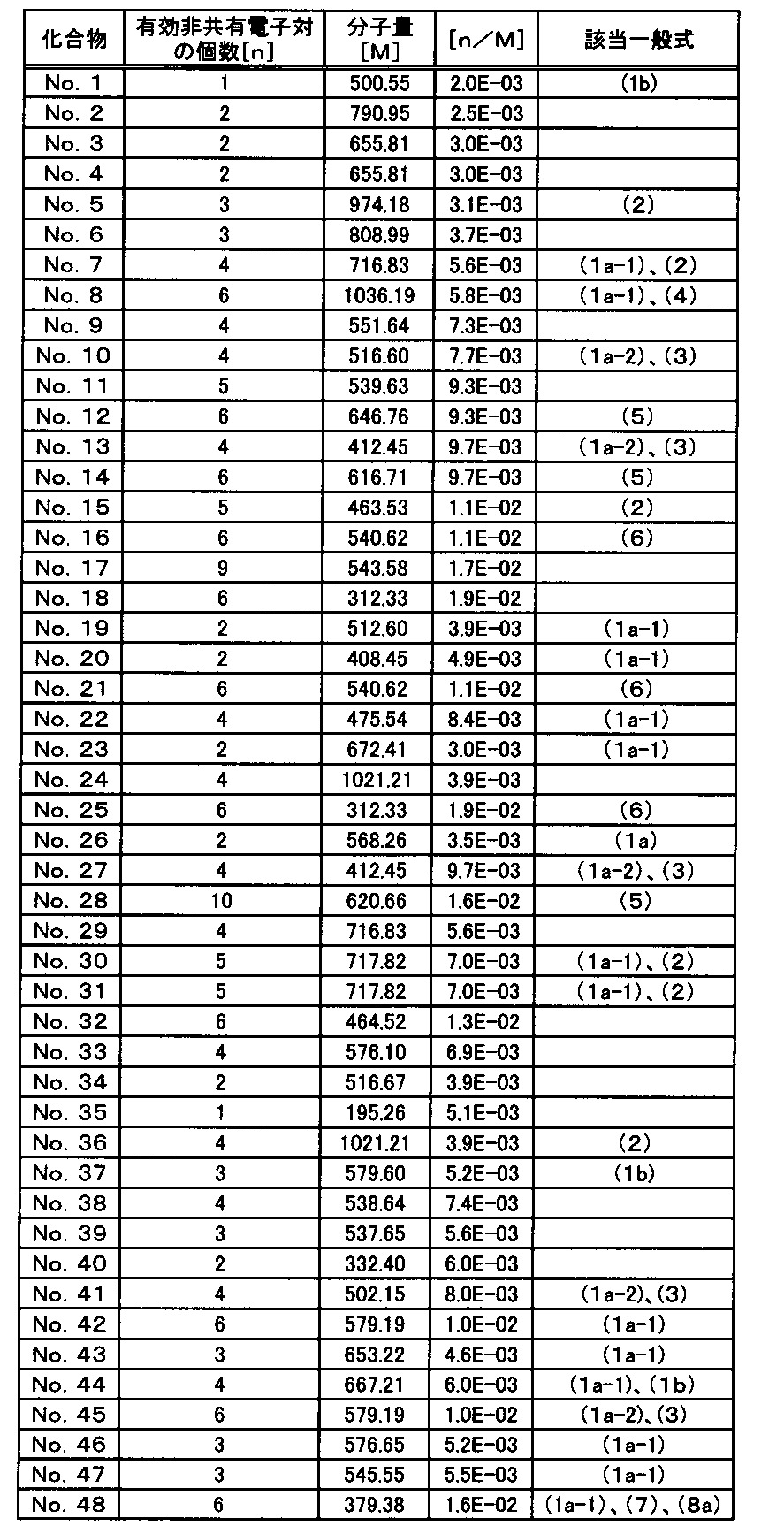
また窒素含有層1aを構成する化合物としては、以上のような有効非共有電子対含有率[n/M]が上述した所定範囲である化合物に加え、他の化合物を用いても良い。窒素含有層1aに用いられる他の化合物は、有効非共有電子対含有率[n/M]が上述した所定範囲で有る無しにかかわらず、窒素原子を含有する化合物が好ましく用いられる。中でも[有効非共有電子対]を有する窒素原子を含有する化合物が特に好ましく用いられる。また、窒素含有層1aに用いられる他の化合物は、この窒素含有層1aを備えた透明電極1が適用される電子デバイスごとに必要とされる性質を有する化合物が用いられる。例えば、この透明電極1が、有機電界発光素子の電極として用いられる場合、その成膜性や、電子輸送性の観点から、窒素含有層1aを構成する化合物として、以降に説明する一般式(1)~(8a)で表される構造を有する化合物が好ましく用いられる。


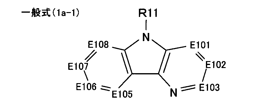
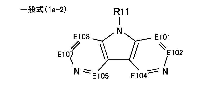
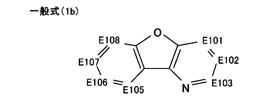
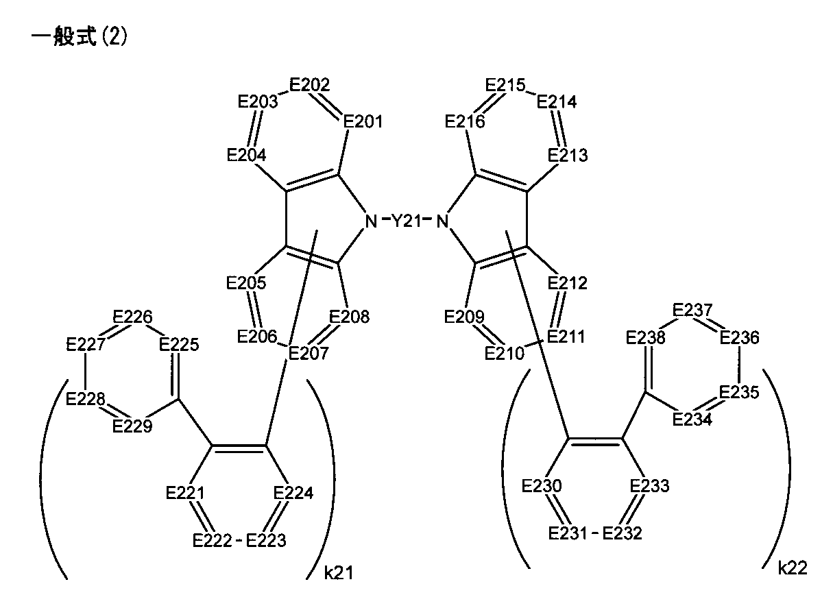
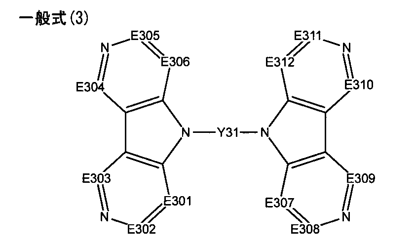
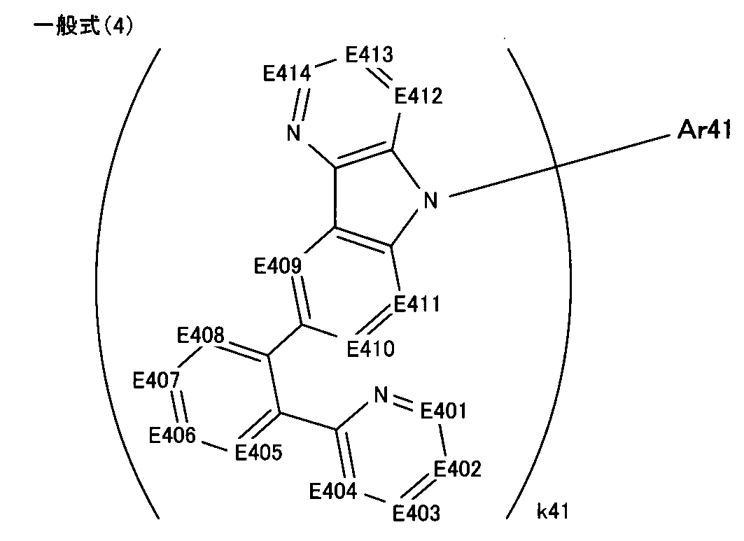

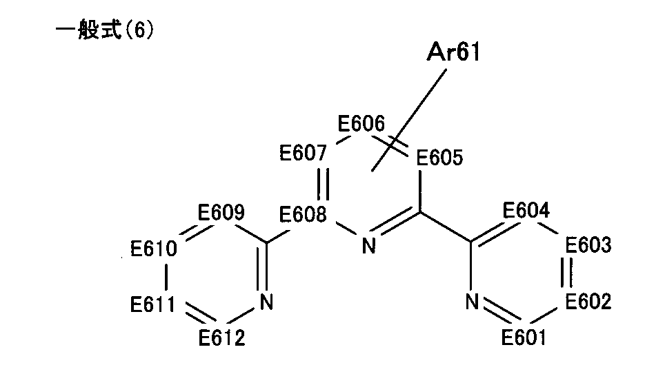
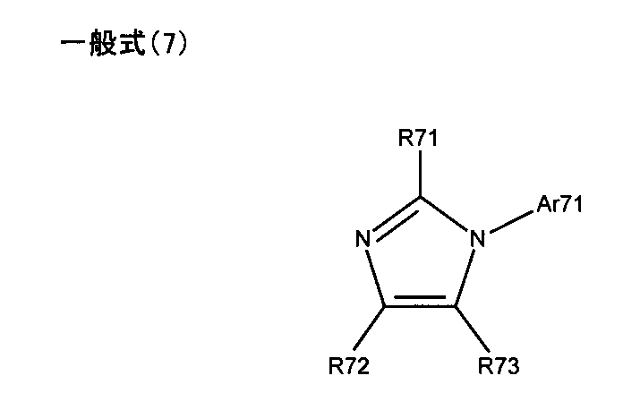

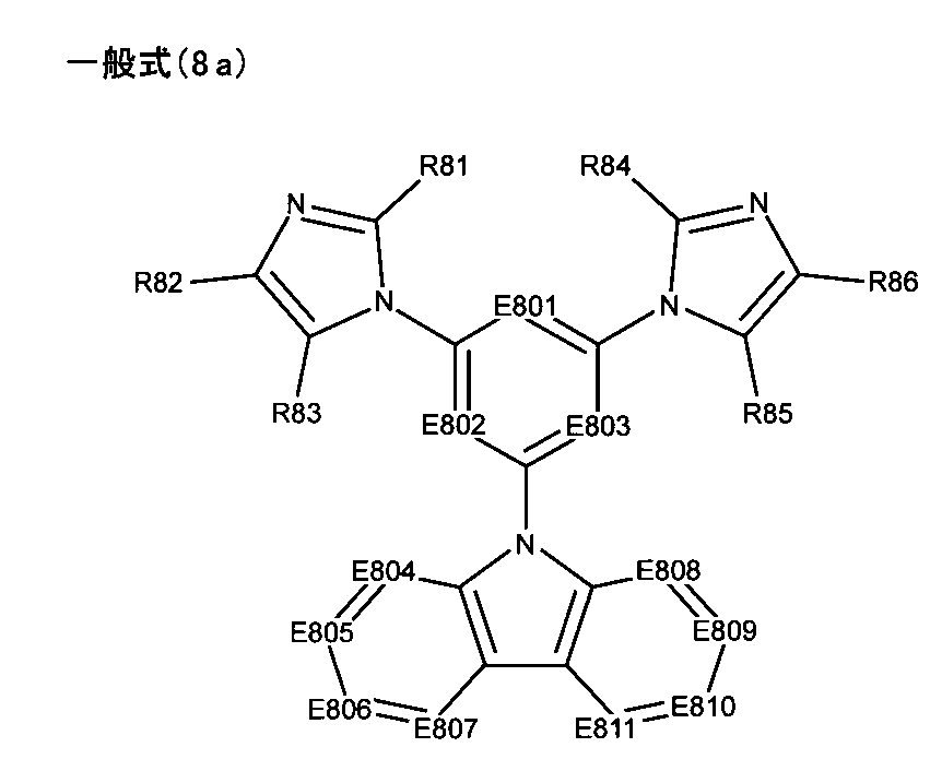
また窒素含有層1aを構成するさらに他の化合物として、以上のような一般式(1)~(8a)で表される構造を有する化合物の他、下記に具体例を示す化合物1~166が例示される。これらの化合物は、電極層1bを構成する銀と相互作用する窒素原子を含有する化合物である。また、これらの化合物は、電子輸送性または電子注入性を備えた材料である。したがって、これらの化合物を用いて窒素含有層1aを構成した透明電極1は、有機電界発光素子における透明電極として好適であり、有機電界発光素子における電子輸送層または電子注入層として窒素含有層1aを用いることができるのである。尚、これらの化合物1~166の中には、上述した有効非共有電子対含有率[n/M]の範囲に当てはまる化合物も含まれ、このような化合物であれば単独で窒素含有層1aを構成する化合物として用いることができる。さらに、これらの化合物1~166の中には、上述した一般式(1)~(8a)に当てはまる化合物もある。
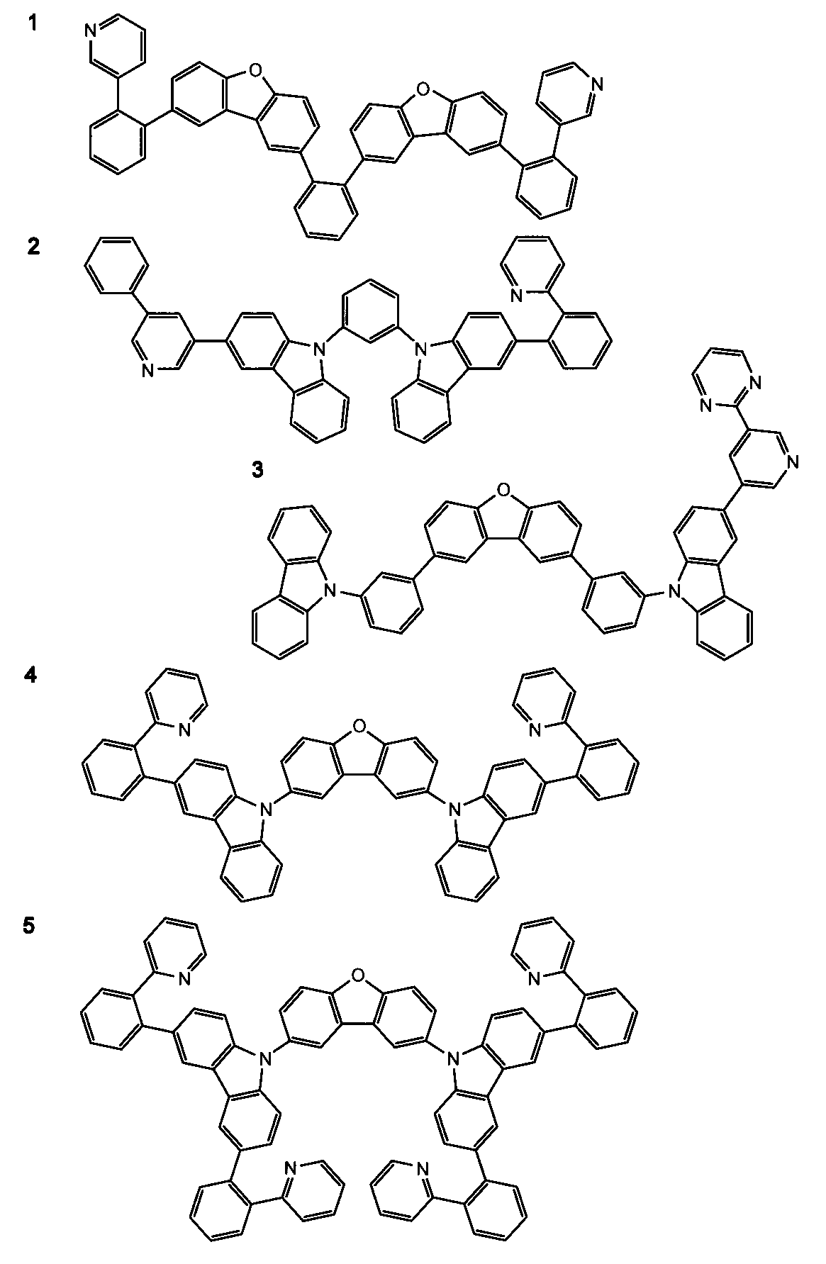
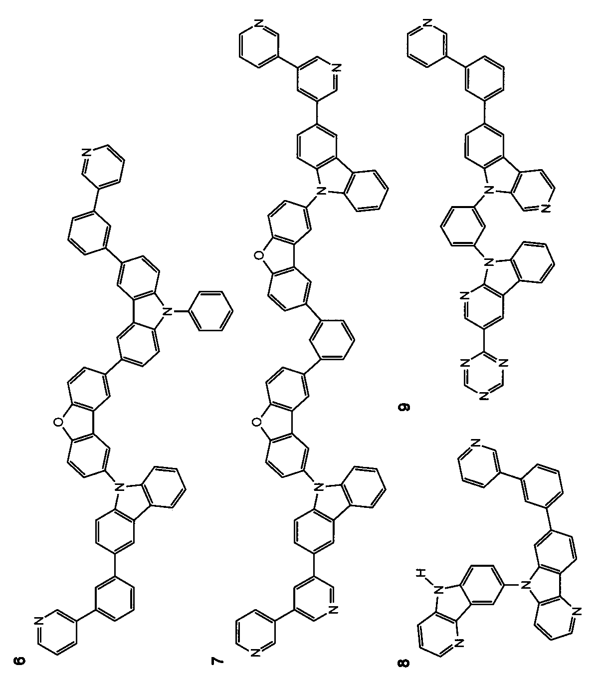
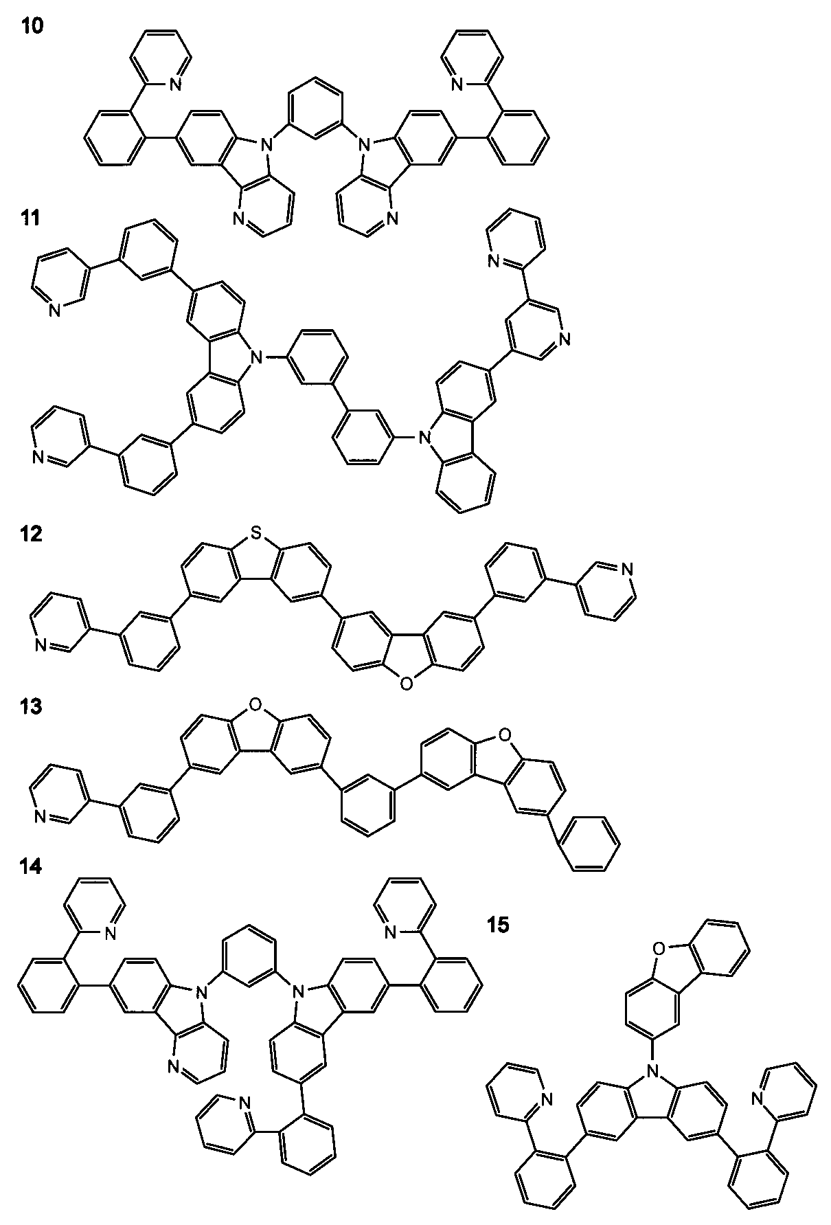
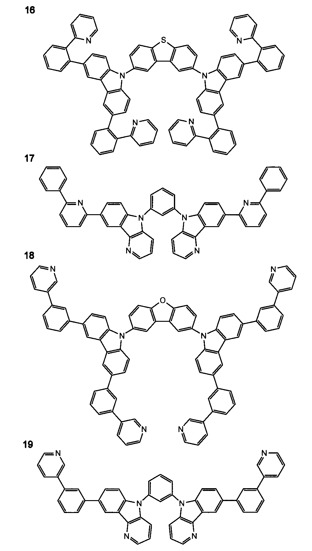

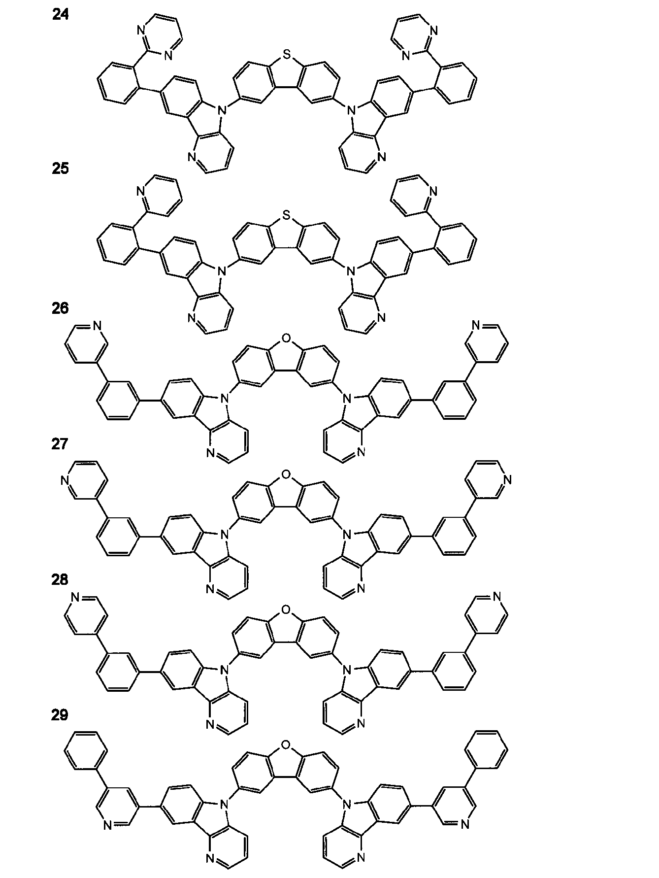
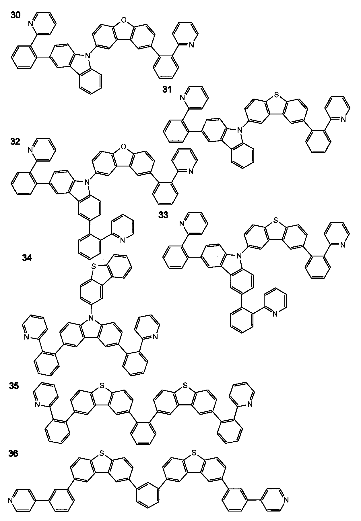


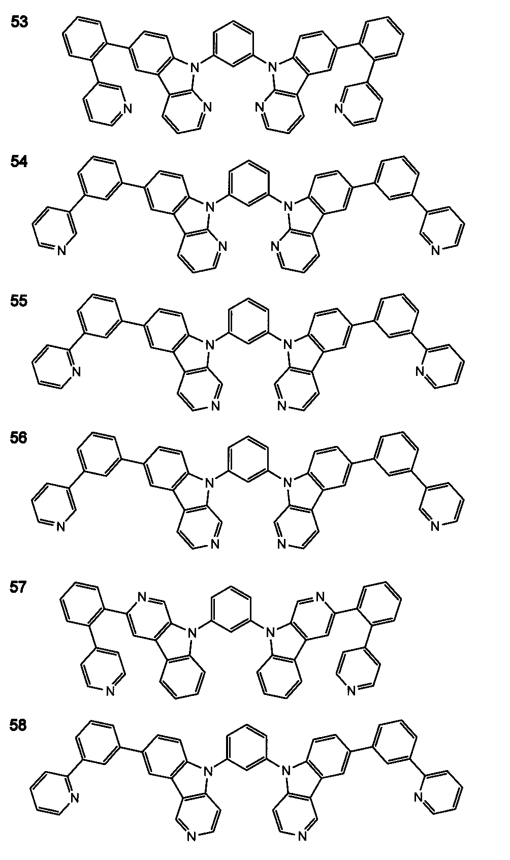

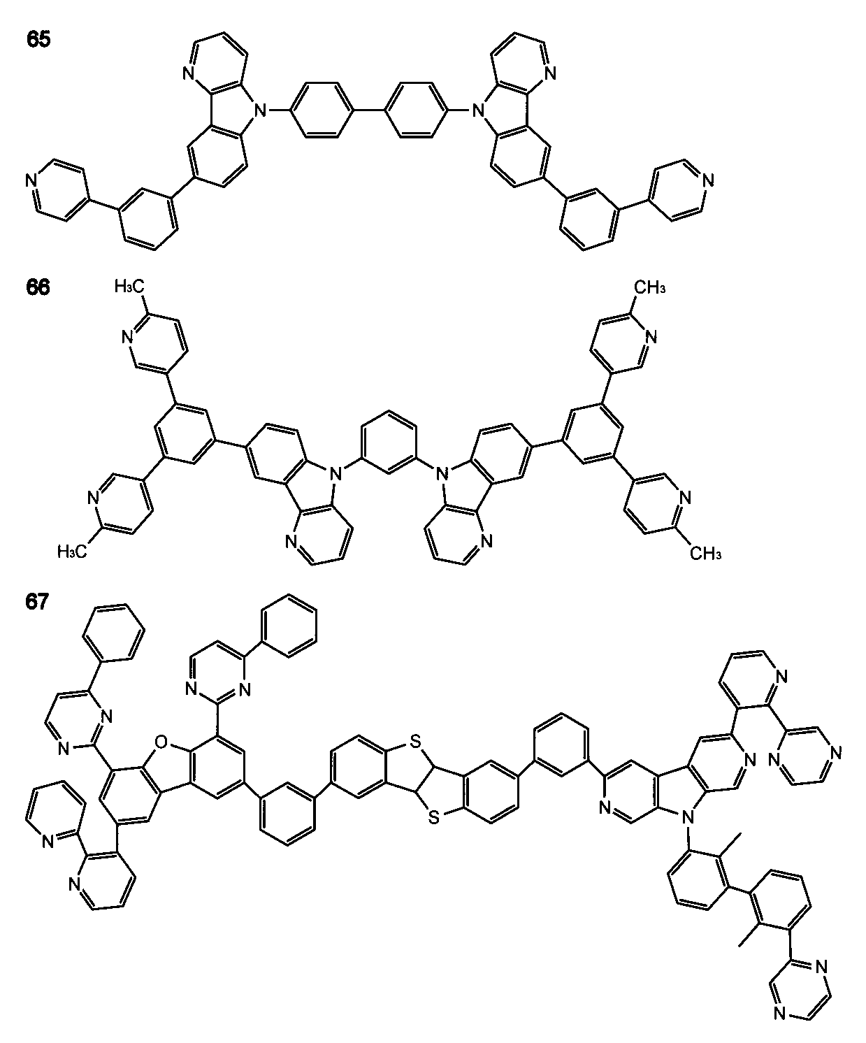

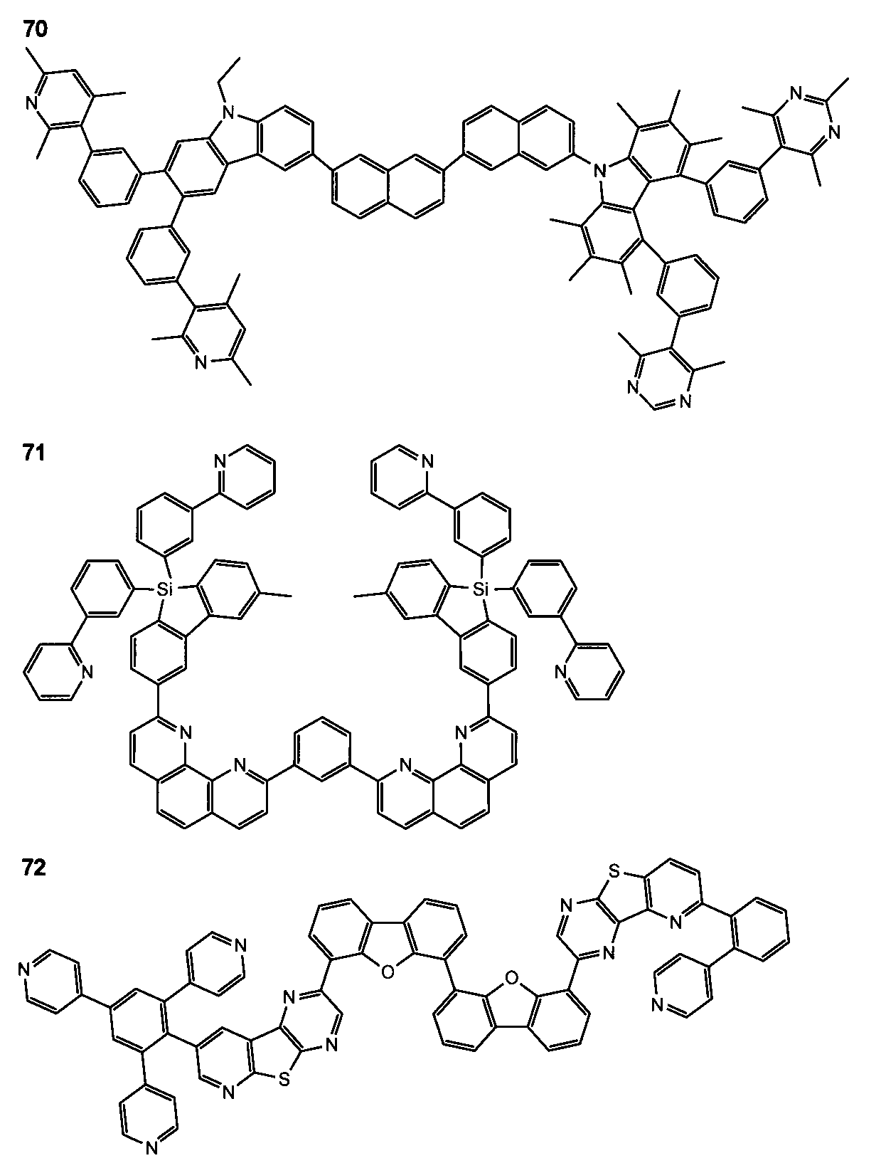
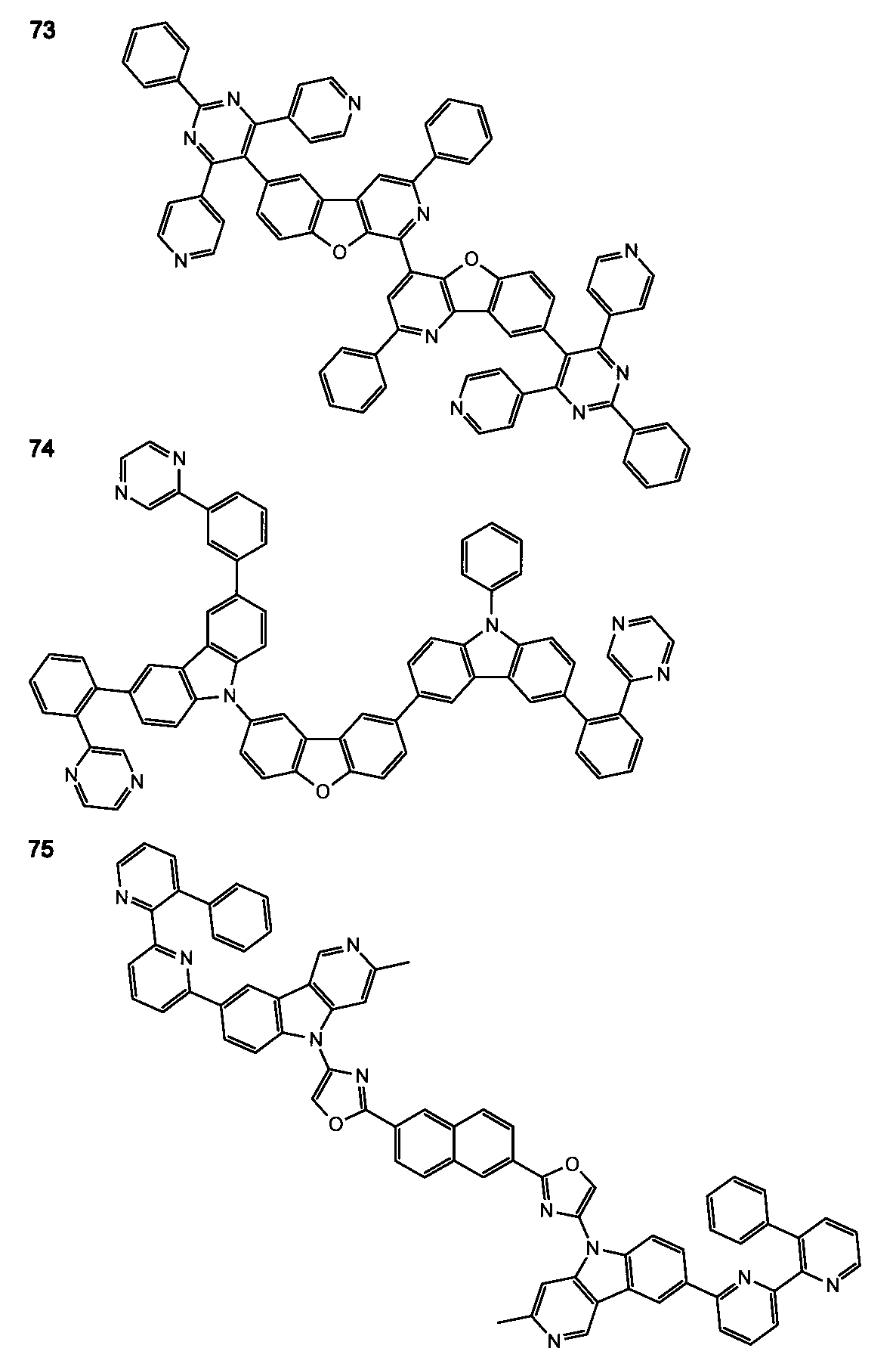

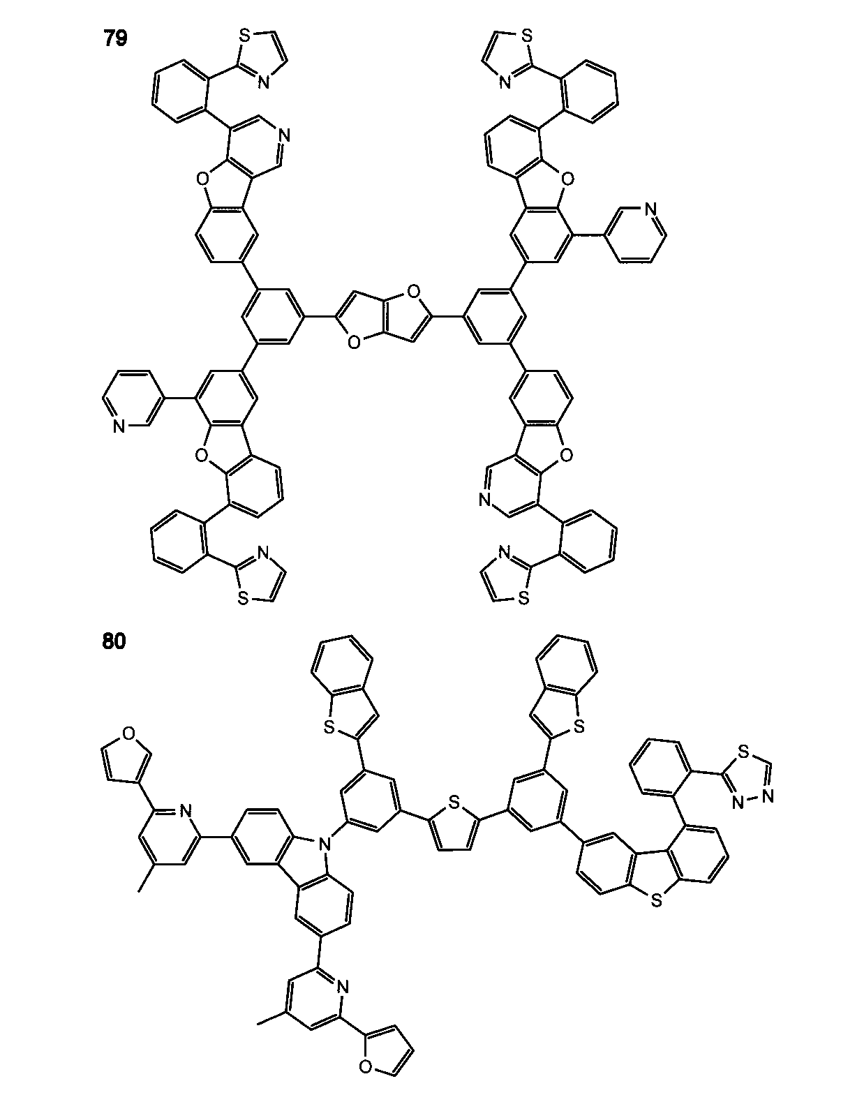
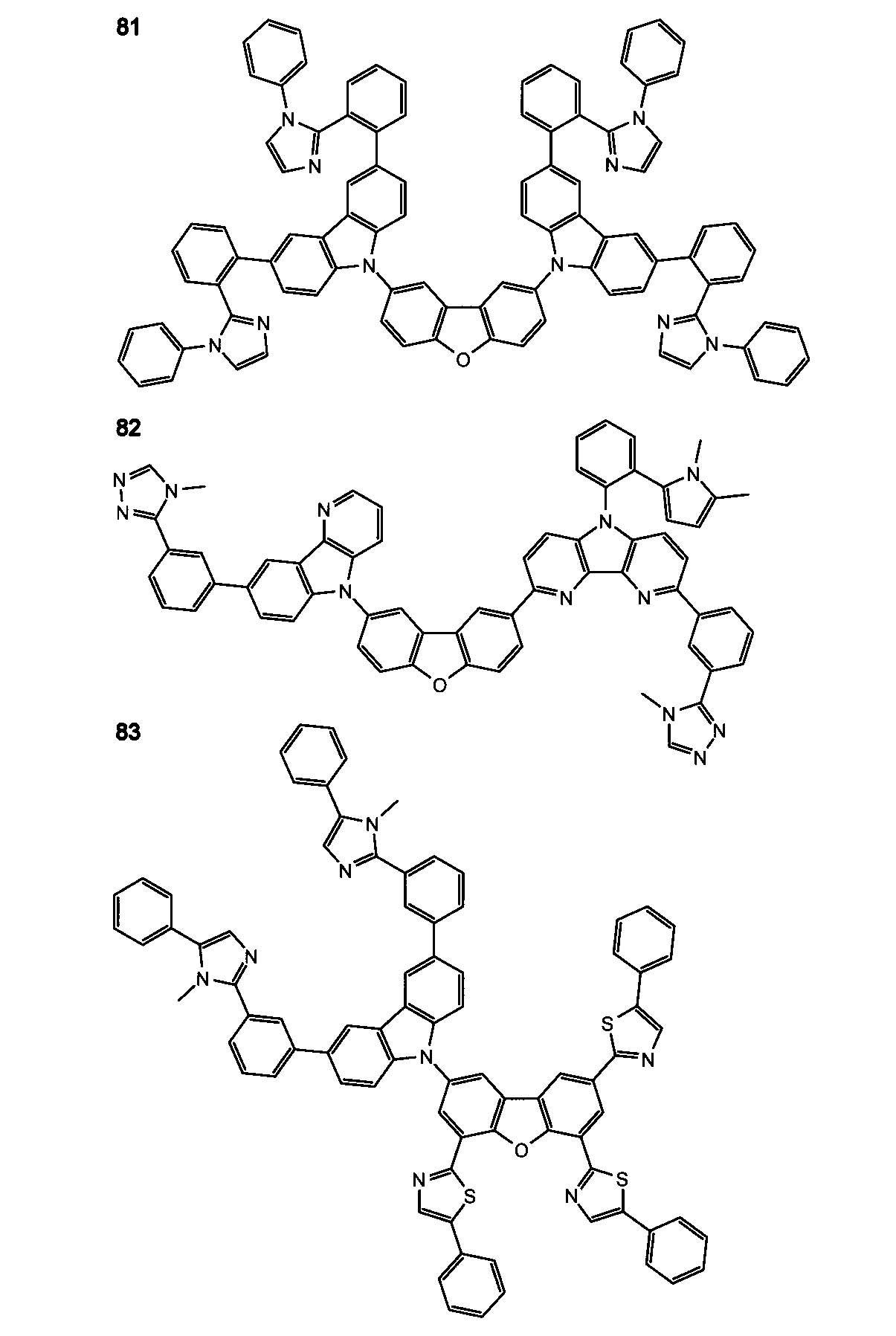
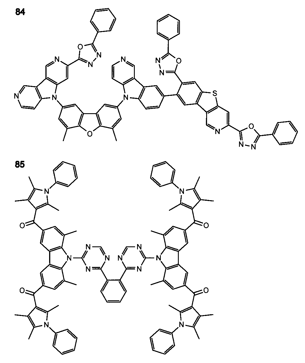
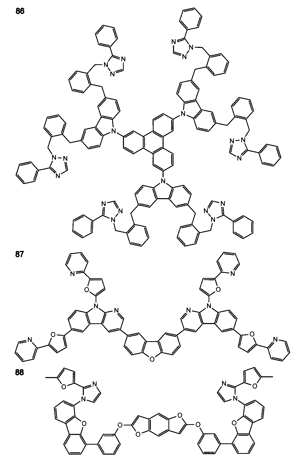
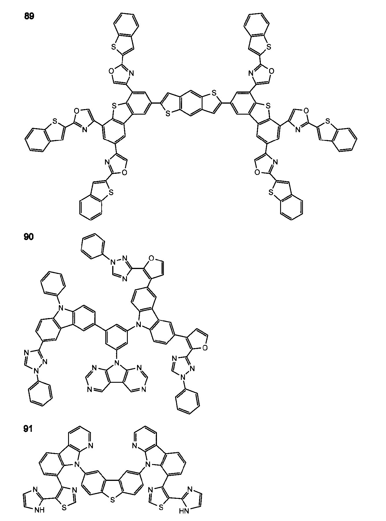
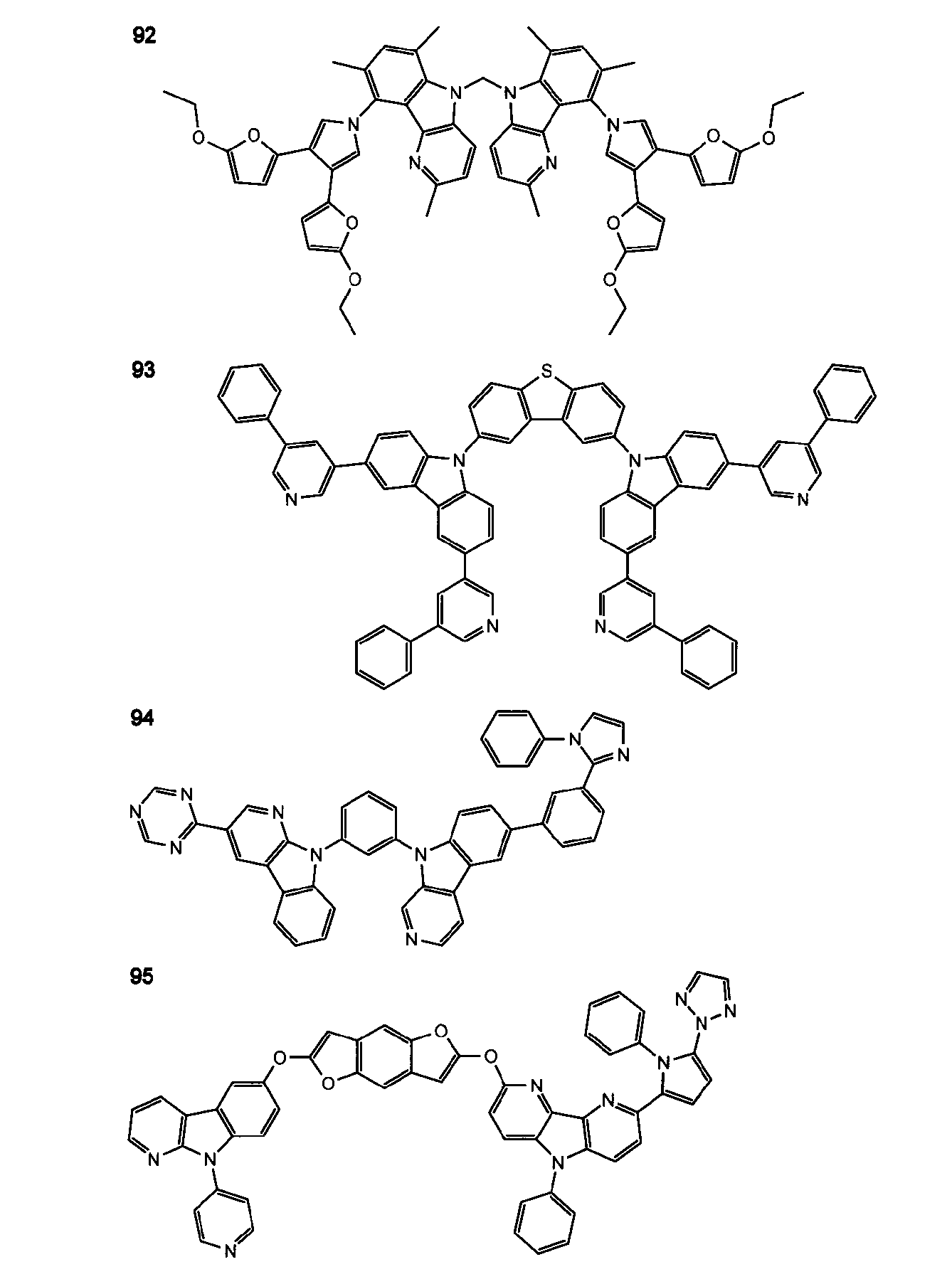

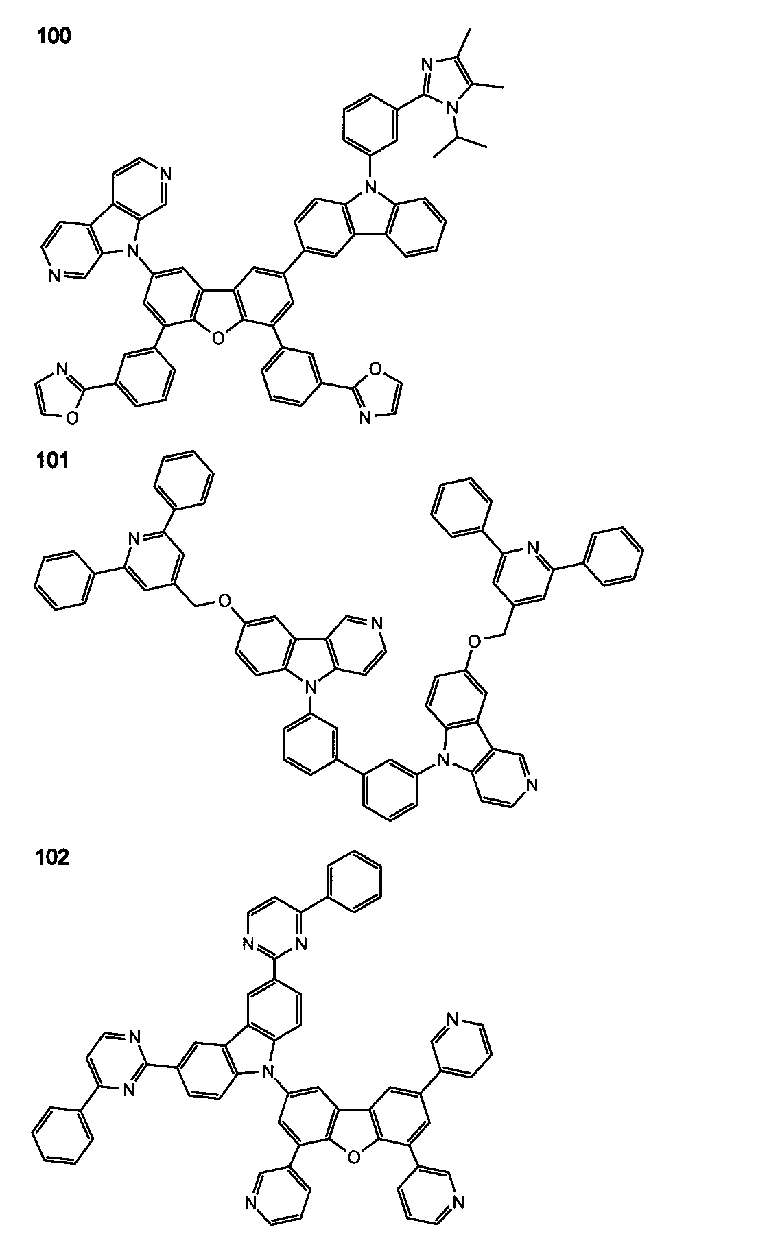
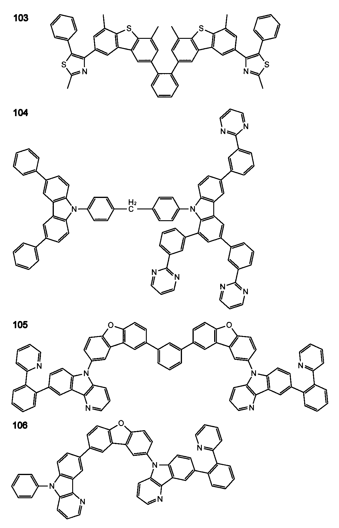
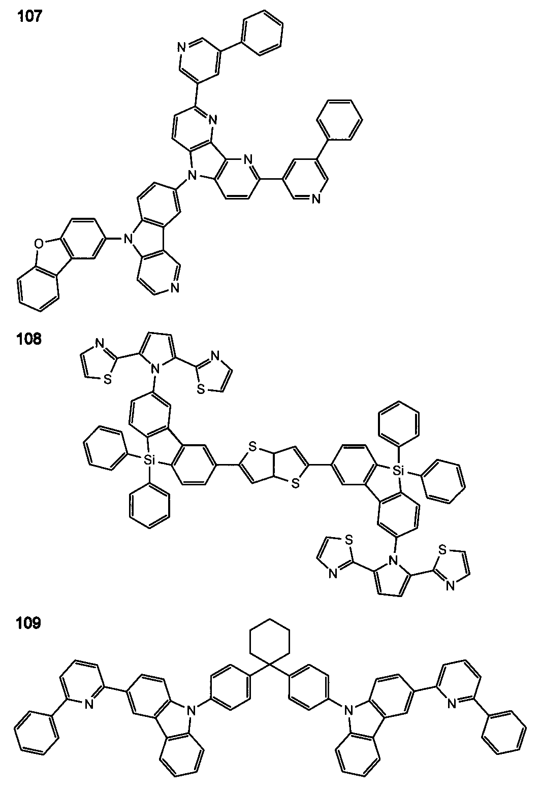


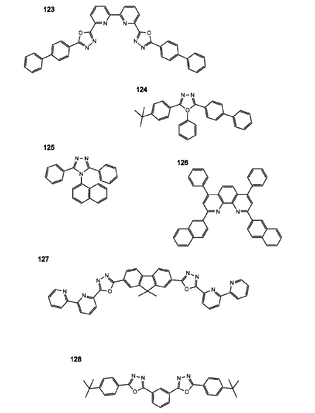


以下に代表的な化合物の合成例として、化合物5の具体的な合成例を示すが、これに限定されない。

窒素雰囲気下、2,8-ジブロモジベンゾフラン(1.0モル)、カルバゾール(2.0モル)、銅粉末(3.0モル)、炭酸カリウム(1.5モル)を、DMAc(ジメチルアセトアミド)300ml中で混合し、130℃で24時間撹拌した。これによって得た反応液を室温まで冷却後、トルエン1Lを加え、蒸留水で3回洗浄し、減圧雰囲気下において洗浄物から溶媒を留去し、その残渣をシリカゲルフラッシュクロマトグラフィー(n-ヘプタン:トルエン=4:1~3:1)にて精製し、中間体1を収率85%で得た。
室温、大気下で中間体1(0.5モル)をDMF(ジメチルホルムアミド)100mlに溶解し、NBS(N-ブロモコハク酸イミド)(2.0モル)を加え、一晩室温で撹拌した。得られた沈殿を濾過し、メタノールで洗浄し、中間体2を収率92%で得た。
窒素雰囲気下、中間体2(0.25モル)、2-フェニルピリジン(1.0モル)、ルテニウム錯体[(η6-C6H6)RuCl2]2(0.05モル)、トリフェニルホスフィン(0.2モル)、炭酸カリウム(12モル)を、NMP(N-メチル-2-ピロリドン)3L中で混合し、140℃で一晩撹拌した。
以上のような窒素含有層1aが基材11上に成膜されたものである場合、その成膜方法としては、塗布法、インクジェット法、コーティング法、ディップ法などのウェットプロセスを用いる方法や、蒸着法(抵抗加熱、EB法など)、スパッタ法、CVD法などのドライプロセスを用いる方法などが挙げられる。なかでも蒸着法が好ましく適用される。
電極層1bは、銀を主成分として構成された層であって、銀または銀を主成分とした合金を用いて構成され、窒素含有層1aに隣接して成膜された層である。
以上のような電極層1bの成膜方法としては、塗布法、インクジェット法、コーティング法、ディップ法などのウェットプロセスを用いる方法や、蒸着法(抵抗加熱、EB法など)、スパッタ法、CVD法などのドライプロセスを用いる方法などが挙げられる。
高屈折率層H1,H2は、窒素含有層1aよりも高い屈折率を有する層である。高屈折率層H1,H2の屈折率は、波長550nmにおける屈折率(n)が、窒素含有層1aの屈折率(n=1.6~1.8)より0.1以上高いと好ましく、0.3以上高いとさらに好ましい。典型的には、波長550nmにおける屈折率(n)が2.0以上の層であることが好ましい。
以上のような高屈折率層H1,H2が基材11上に成膜されたものである場合、その成膜方法としては、蒸着法(抵抗加熱、EB法など)またはスパッタ法が挙げられる。特に、EB蒸着であれば、イオンアシストを用いた方法が好適である。このような高屈折率層H1,H2の成膜方法は、これを構成する材料によって適切な方法が選択されることとする。例えば、酸化亜鉛(ZnO)または酸化チタン(TiO2)を用いた高屈折率層H1,H2の成膜であれば蒸着法が適用される。また酸化インジウム(In2O3)、酸化インジウムスズ(ITO)、または酸化ニオブ(Nb2O5)を用いた高屈折率層H1,H2の成膜であればスパッタ法が適用される。
以上のように構成された透明電極1は、窒素原子を含有する化合物を用いて構成された窒素含有層1aに隣接させて、銀を主成分とした電極層1bを設けた構成である。これにより、窒素含有層1aに隣接させて電極層1bを成膜する際には、電極層1bを構成する銀原子が窒素含有層1aを構成する窒素原子を含んだ化合物と相互作用し、銀原子の窒素含有層1a表面においての拡散距離が減少し、銀の凝集が抑えられる。このため、一般的には核成長型(Volumer-Weber:VW型)での膜成長により島状に孤立し易い銀薄膜が、単層成長型(Frank-van der Merwe:FM型)の膜成長によって成膜されるようになる。したがって、薄い膜厚でありながらも、均一な膜厚の電極層1bが得られるようになる。
上述した構成の透明電極1は、各種電子デバイスに用いることができる。電子デバイスの例としては、有機電界発光素子、LED(light Emitting Diode)、液晶素子、太陽電池、タッチパネル等が挙げられ、これらの電子デバイスにおいて光透過性を必要とされる電極部材として、上述の透明電極1を用いることができる。
<透明電極を用いた有機電界発光素子の構成>
図7は、本発明の電子デバイスの一例として、上述した透明電極1を用いた有機電界発光素子の一構成例を示す断面構成図である。以下にこの図に基づいて有機電界発光素子の構成を説明する。
尚、図7に示した例では、透明電極1がアノード(すなわち陽極)側に配置された構成であるが、カソード(すなわち陰極)として用いられることで逆積み型としてもよい。
以下、本発明の有機電界発光素子ELにおける代表的な構成としては、以下の構成を挙げることができるが、これらに限定されるものではない。
(1)陽極/発光層/陰極
(2)陽極/発光層/電子輸送層/陰極
(3)陽極/正孔輸送層/発光層/陰極
(4)陽極/正孔輸送層/発光層/電子輸送層/陰極
(5)陽極/正孔輸送層/発光層/電子輸送層/電子注入層/陰極
(6)陽極/正孔注入層/正孔輸送層/発光層/電子輸送層/陰極
(7)陽極/正孔注入層/正孔輸送層/(電子阻止層/)発光層/(正孔阻止層/)電子輸送層/電子注入層/陰極
上記の中で(7)の構成が好ましく用いられるが、これに限定されるものではない。上記の代表的な素子構成において、陽極と陰極を除く層が、発光性を有する発光機能層3である。また、陽極又は陰極は、本願の透明電極1又は対向電極5のいずれかで構成する。
発光機能層3は、透明電極1と対向電極5との間に挟持された層であって、透明電極1及び対向電極5とともに有機電界発光素子ELを構成している。この発光機能層3は、一般的な有機電界発光素子における発光機能層の層構造であって良く、有機材料で構成された発光層3cを有することが必須である。
また、電子輸送層3d及び正孔輸送層3bは、複数層で構成されていてもよい。
また、有機電界発光素子は、少なくとも1層の発光層を含む発光ユニットを複数積層した、いわゆるタンデム構造の素子であってもよい。
(1.1)陽極/第1発光ユニット/中間層/第2発光ユニット/陰極
(2.2)陽極/第1発光ユニット/中間層/第2発光ユニット/中間層/第3発光ユニット/陰極
発光層3cは、電極または隣接層から注入されてくる電子及び正孔が再結合し、励起子を経由して発光する場を提供する層であり、発光する部分は発光層3cの層内であっても、発光層3cと隣接層との界面であってもよい。本発明に係る発光層3cは、本発明で規定する要件を満たしていれば、その構成に特に制限はない。
発光層3cに用いられる発光ドーパントについて説明する。
発光ドーパントとしては、蛍光発光性ドーパント(蛍光ドーパント、蛍光性化合物ともいう)と、リン光発光性ドーパント(リン光ドーパント、リン光性化合物ともいう)が好ましく用いられる。本発明においては、少なくとも1層の発光層3cがリン光発光ドーパントを含有することが好ましい。
白色を示す発光ドーパントの組み合わせについては特に限定はないが、例えば青と橙や、青と緑と赤の組み合わせ等が挙げられる。
本発明の有機電界発光素子ELにおける白色とは、2度視野角正面輝度を前述の方法により測定した際に、1000cd/m2でのCIE1931表色系における色度がx=0.39±0.09、y=0.38±0.08の領域内にあることが好ましい。
リン光発光性ドーパント(以下、「リン光ドーパント」という)について説明する。
本発明に係るリン光ドーパントは、励起三重項からの発光が観測される化合物であり、具体的には、室温(25℃)にてリン光発光する化合物であり、リン光量子収率が、25℃において0.01以上の化合物であると定義されるが、好ましいリン光量子収率は0.1以上である。
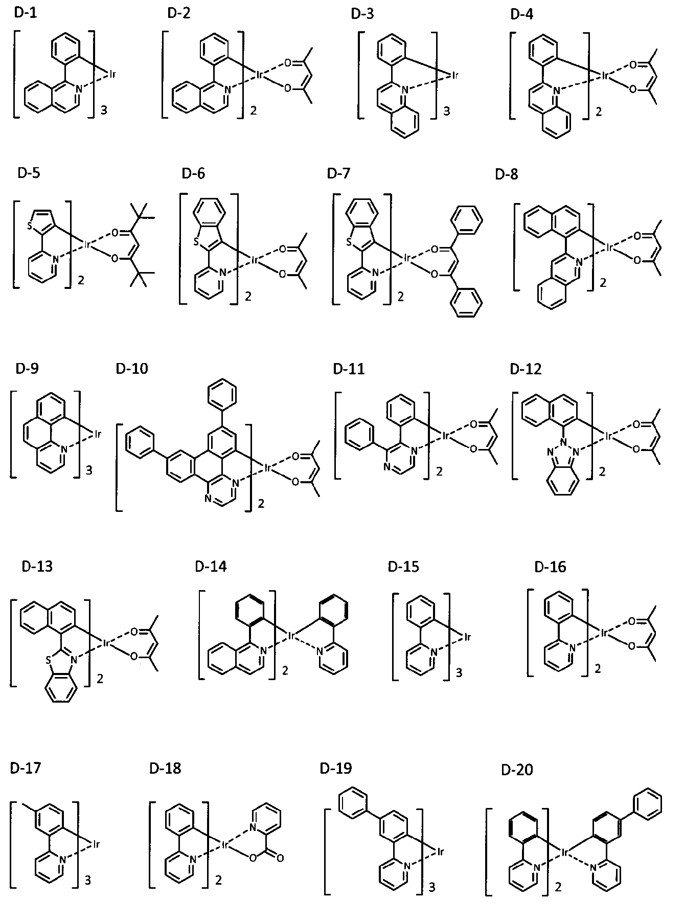
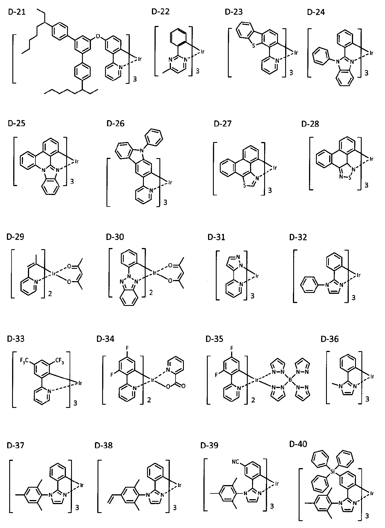
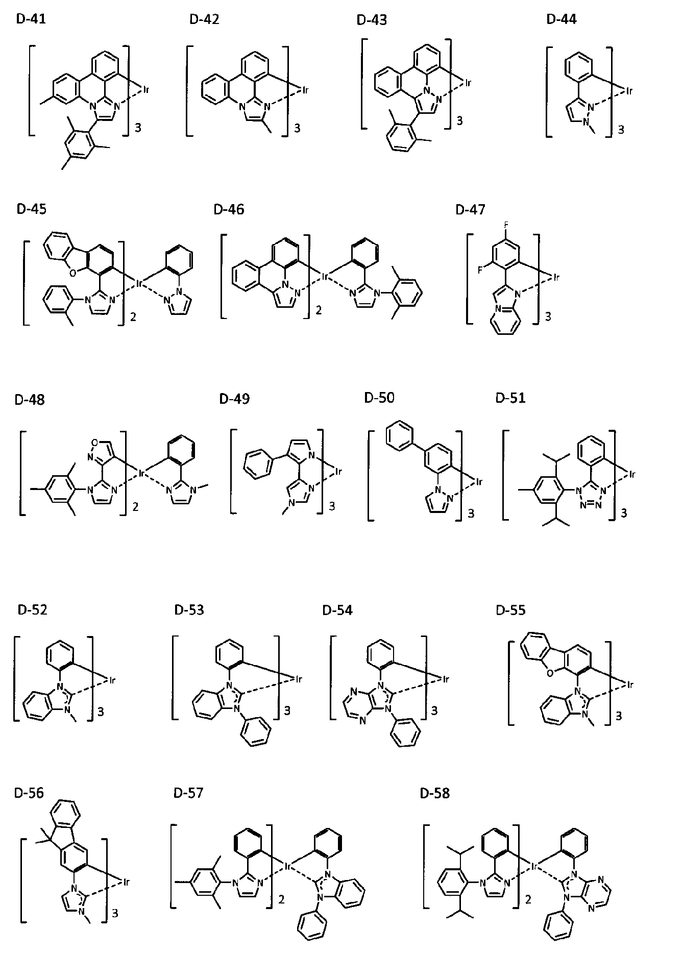

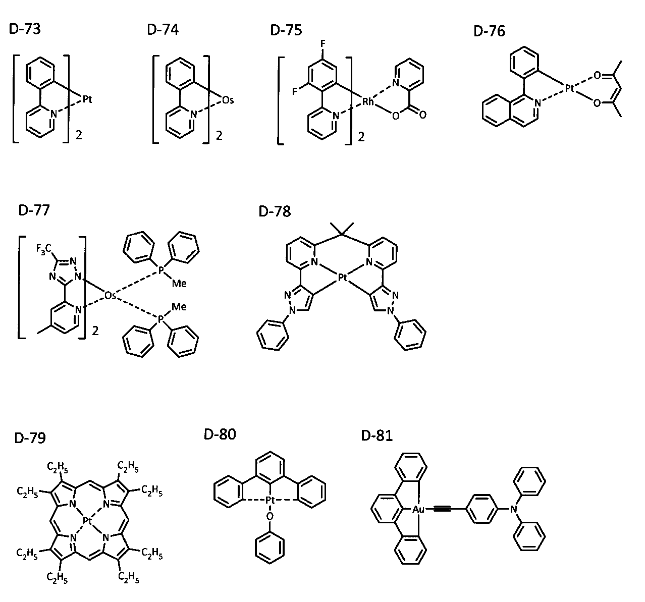
蛍光発光性ドーパント(以下、「蛍光ドーパント」という)について説明する。
また、近年では遅延蛍光を利用した発光ドーパントも開発されており、これらを用いてもよい。
ホスト化合物は、発光層3cにおいて主に電荷の注入および輸送を担う化合物であり、有機電界発光素子ELにおいてそれ自体の発光は実質的に観測されない。
好ましくは室温(25℃)においてリン光発光のリン光量子収率が、0.1未満の化合物であり、さらに好ましくはリン光量子収率が0.01未満の化合物である。また、発光層3cに含有される化合物の内で、その層中での質量比が20%以上であることが好ましい。
ここで、ガラス転移点(Tg)とは、DSC(Differential Scanning Colorimetry:示差走査熱量法)を用いて、JIS-K-7121に準拠した方法により求められる値である。
有機電界発光素子ELに用いる電子輸送とは、電子を輸送する機能を有する材料からなり、陰極より注入された電子を発光層3cに伝達する機能を有する。
電子輸送材料は単独で用いてもよく、また複数種を併用して用いてもよい。電子輸送層3dの総厚については特に制限はないが、通常は2nm~5μmの範囲であり、より好ましくは2nm~500nmであり、さらに好ましくは5nm~200nmである。
芳香族炭化水素環誘導体としては、ナフタレン誘導体、アントラセン誘導体、トリフェニレン等が挙げられる。
また、これらの材料を高分子鎖に導入した、またはこれらの材料を高分子の主鎖とした高分子材料を用いることもできる。
正孔阻止層は、広い意味では電子輸送層3dの機能を有する層である。好ましくは、電子を輸送する機能を有しつつ、正孔を輸送する能力が小さい材料からなる。電子を輸送しつつ正孔を阻止することで、電子と正孔の再結合確率を向上させることができる。
また、上述の電子輸送層3dの構成を、必要に応じて正孔阻止層として用いることができる。
正孔阻止層に用いられる材料としては、上述の電子輸送層3dに用いられる材料が好ましく用いられ、また、上述のホスト化合物として用いられる材料も正孔阻止層に好ましく用いられる。
電子注入層3e(「陰極バッファー層」ともいう)は、駆動電圧低下や発光輝度向上のために陰極と発光層3cとの間に設けられる層である。電子注入層3eの一例は、「有機EL素子とその工業化最前線(1998年11月30日エヌ・ティー・エス社発行)」の第2編第2章「電極材料」(123~166頁)に記載されている。
電子注入層3eはごく薄い膜であることが好ましく、素材にもよるがその膜厚は0.1nm~5nmの範囲が好ましい。また構成材料が断続的に存在する不均一な膜であってもよい。
また、上記の電子注入層3eに用いられる材料は単独で用いてもよく、複数種を併用して用いてもよい。
正孔輸送層3bは、正孔を輸送する機能を有する材料からなる。正孔輸送層3bは、陽極より注入された正孔を発光層3cに伝達する機能を有する層である。
電子阻止層は、広い意味では正孔輸送層3bの機能を有する層である。好ましくは、正孔を輸送する機能を有しつつ電子を輸送する能力が小さい材料からなる。電子阻止層は、正孔を輸送しつつ電子を阻止することで、電子と正孔の再結合確率を向上させることができる。
正孔注入層3a(「陽極バッファー層」ともいう)は、駆動電圧低下や発光輝度向上のために陽極と発光層3cとの間に設けられる層である。正孔注入層3aの一例は、「有機EL素子とその工業化最前線(1998年11月30日エヌ・ティー・エス社発行)」の第2編第2章「電極材料」(123~166頁)に記載されている。
正孔注入層3aは必要に応じて設けられ、上述のように陽極と発光層3cとの間、又は、陽極と正孔輸送層3bとの間に設けられる。
正孔注入層3aに用いられる材料は、例えば上述の正孔輸送層3bに用いられる材料等が挙げられる。中でも、銅フタロシアニンに代表されるフタロシアニン誘導体、特表2003-519432号や特開2006-135145号等に記載されているようなヘキサアザトリフェニレン誘導体、酸化バナジウムに代表される金属酸化物、アモルファスカーボン、ポリアニリン(エメラルディン)やポリチオフェン等の導電性高分子、トリス(2-フェニルピリジン)イリジウム錯体等に代表されるオルトメタル化錯体、トリアリールアミン誘導体等が好ましい。
上述の正孔注入層3aに用いられる材料は単独で用いてもよく、また複数種を併用して用いてもよい。
有機電界発光素子ELを構成する発光機能層3は、更に他の含有物を含んでもよい。
含有物としては、例えば臭素、ヨウ素及び塩素等のハロゲン元素やハロゲン化化合物、Pd、Ca、Na等のアルカリ金属やアルカリ土類金属、遷移金属の化合物や錯体、塩等が挙げられる。
ただし、電子や正孔の輸送性を向上させる目的や、励起子のエネルギー移動を有利にするための目的などによってはこの範囲内ではない。
有機電界発光素子ELの発光機能層(正孔注入層、正孔輸送層、発光層、正孔阻止層、電子輸送層、電子注入層等)の形成方法について説明する。尚、発光機能層3の形成方法は、特に制限はなく、従来公知の例えば真空蒸着法、湿式法(ウェットプロセス)等により形成することができる。
また、層毎に異なる形成方法を適用してもよい。
透明電極1は、先に説明した図1の透明電極1であり、有機電界発光素子ELの陽極又は陰極を構成する。
対向電極5は、有機電界発光素子ELの陽極又は陰極を構成する電極であって、発光機能層3を介して透明電極1の一主面上に設けられた電極である。この対向電極5は、有機電界発光素子ELの発光機能層3に対して、透明電極1が陽極であれば陰極として用いられ、透明電極1が陰極であれば陽極として用いられる。このため、少なくとも発光機能層3に接する側の界面層が、陰極または陽極として適する材料で構成されていることとする。
有機電界発光素子ELにおける陽極としては、仕事関数の大きい(4eV以上、好ましくは4.5V以上)金属、合金、電気伝導性化合物、及び、これらの混合物からなる電極物質が用いられる。このような電極物質の具体例としては、Au等の金属、CuI、インジウムチンオキシド(ITO)、SnO2、ZnO等の導電性透明材料が挙げられる。また、IDIXO(In2O3-ZnO)等非晶質で透明導電膜を作製可能な材料を用いてもよい。
陰極としては、仕事関数の小さい(4eV以下)金属(電子注入性金属と称する)、合金、電気伝導性化合物、及び、これらの混合物からなる電極物質が用いられる。このような電極物質の具体例としては、ナトリウム、ナトリウム-カリウム合金、マグネシウム、リチウム、マグネシウム/銅混合物、マグネシウム/銀混合物、マグネシウム/アルミニウム混合物、マグネシウム/インジウム混合物、アルミニウム/酸化アルミニウム(Al2O3)混合物、インジウム、リチウム/アルミニウム混合物、アルミニウム、希土類金属等が挙げられる。
室温における有機電界発光素子ELの発光の外部取り出し効率は、1%以上であることが好ましく、5%以上であるとより好ましい。
ここで、外部取り出し量子効率(%)=有機電界発光素子外部に発光した光子数/有機電界発光素子に流した電子数×100である。
また、カラーフィルター等の色相改良フィルター等を併用しても、有機電界発光素子ELからの発光色を蛍光体により多色へ変換する色変換フィルターを併用してもよい。
有機電界発光素子ELは少ない電力で良好発光するものの、水分に弱く、水分吸水により非発光部ができてしまうため、封止材17により封止することが好ましい。
封止材17を凹状に加工するのは、サンドブラスト加工、化学エッチング加工等が使われる。
有機電界発光素子ELを封止する封止膜又は封止用フィルムの外側には、素子の機械的強度を高めるために、保護膜又は保護板を設けてもよい。特に、封止膜により有機電界発光素子ELの封止が行われている場合には、機械的強度が必ずしも高くないため、保護膜又は保護板を設けることが好ましい。保護膜又は保護板として使用することが可能な材料は、例えば、上述の封止材17と同様に、ガラス板、ポリマー板・フィルム、金属板・フィルム等を用いることができる。保護膜又は保護板としては、軽量化及び薄膜化が可能なポリマーフィルムを用いることが好ましい。
有機電界発光素子ELは、空気よりも屈折率の高い層(屈折率1.6~2.1程度の範囲内)の内部で発光し、発光層3cで発生した光のうち15%から20%程度の光しか取り出せないことが一般的に知られている。この理由として、臨界角以上の角度θで界面(例えば透明基板13と空気との界面)に入射する光は、全反射を起こし素子外部に取り出すことが難しいことや、透明基板13と透明電極1、又は透明電極1と発光層3cとの間で光が全反射を起こし、光が透明電極1ないし発光層3cを導波し、結果として、光が素子側面方向に逃げるためである。
有機電界発光素子ELにおいては、これらの手段を組み合わせることにより、更に光の取り出し効率を向上することができる。
有機電界発光素子ELは、光取り出し面側に、例えばマイクロレンズアレイや、所謂集光シート設けることにより、特定方向、例えば素子発光面に対し正面方向に集光して、特定方向上の輝度を高めることができる。
有機電界発光素子ELは、表示デバイス、ディスプレイ、各種発光光源などの電子機器に適用することができる。
照明装置に用いる有機電界発光素子は、上述した構成の有機電界発光素子ELに共振器構造を持たせた設計としてもよい。共振器構造として構成された有機電界発光素子の使用目的としては、光記憶媒体の光源、電子写真複写機の光源、光通信処理機の光源、光センサーの光源等が挙げられるが、これらに限定されない。また、レーザー発振をさせることにより上記用途に使用してもよい。
以上説明した有機電界発光素子ELは、本発明の導電性と光透過性とを兼ね備えると共に信頼性の向上が図られた透明電極1をアノードとして用い、この透明電極1における高屈折率層H2側に発光機能層3とカソードとなる対向電極5とをこの順に設けた構成である。このため、透明電極1と対向電極5との間に十分な電圧を印加して有機電界発光素子ELでの高輝度発光を実現しつつ、透明電極1側からの発光光hの取り出し効率が向上することによる高輝度化を図ることが可能である。しかも、このような性能を長期的に維持することができ、長期信頼性の向上をも図ることが可能である。さらに、所定輝度を得るための駆動電圧の低減によっても、発光寿命の向上が図られる。
以降の表2に構成を示すように、試料101~137の各透明電極を、導電性領域の面積が5cm×5cmとなるように作製した。
以下のようにして、ガラス製の基材上に、下記表2に示すそれぞれの膜厚で銀(Ag)からなる電極層を形成した。
以下のようにして下記表2に示すそれぞれの材料で構成された高屈折率層で電極層を挟持した構成の透明電極を作製した。
以下のようにして、ガラス製の基材上に、銀(Ag)にアルミニウム(Al)を添加した電極層を形成した。
以下のようにして、ガラス製の基材上に、下記表2に示すそれぞれの材料を用いた窒素を含有する窒素含有層と、銀からなる電極層との2層構造の透明電極を形成した。尚、試料106では、窒素含有層に換えて窒素を含有しない下地層を形成した。
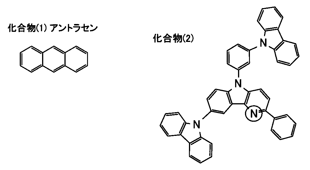
下記表2を参照し、ガラス製の基材上に、高屈折率層、窒素含有層、銀(Ag)を主成分とする電極層、および高屈折率層をこの順に積層した透明電極を作製した。
試料122,129の作製で説明した手順において、基材をポリエチレンテレフタレート(PET)製の基材を用いて形成した以外は、上記試料122,129と同様の手順で、試料136,137の各透明電極を作製した。
上記で作製した試料101~137の各透明電極について、(1)波長550nmの光に対する光透過率、(2)シート抵抗、および(3)高温・高湿保存性を測定した。
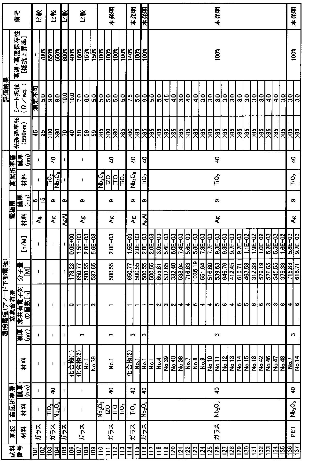
表2から明らかなように、試料110~137の各透明電極、すなわち高屈折率層、窒素含有層、銀(Ag)を主成分とする電極層、および高屈折率層がこの順に積層された透明電極は、光透過率が80%以上であるにもかかわらず、シート抵抗値も10Ω/sq.未満であり、高温・高湿保存性も140%以下であり、導電性の向上と光透過性の向上との両立と共に、信頼性の向上を図られた透明電極であることが確認された。
以降の表3に構成を示すように、各構成の透明電極をアノードとして発光機能層の下部に設けた試料201~229のボトムエミッション型の各有機電界発光素子を作製した。図9を参照し、作製手順を説明する。尚、下記表3には、試料201~229の有機電界発光素子に用いた透明電極の構成を示した。
(透明電極1’の形成)
先ず試料201~229において、ポリエチレンテレフタレート(PET)製の透明基板13の上部に、下記表3に示した各構成の透明電極1’を形成した。各構造の透明電極の形成手順は、実施例1で対応する構造の透明電極の作製と同様に行った。各構成の透明電極1’のうち、試料208~229では、本発明構成の透明電極1となる。
正孔輸送注入材料として下記構造式に示すα-NPDが入った加熱ボートに通電して加熱し、α-NPDよりなる正孔注入層と正孔輸送層とを兼ねた正孔輸送・注入層31を、透明電極1’上に成膜した。この際、蒸着速度0.1nm/秒~0.2nm/秒、膜厚20nmとした。

次に、下記構造式に示すホスト材料H-1の入った加熱ボートと、下記構造式に示す燐光発光性化合物Ir1の入った加熱ボートとを、それぞれ独立に通電し、ホスト材料H-1と燐光発光性化合物Ir1とからなる発光層32を、正孔輸送・注入層31上に成膜した。この際、蒸着速度がホスト材料H-1:燐光発光性化合物Ir1=100:6となるように、加熱ボートの通電を調節した。また膜厚30nmとした。
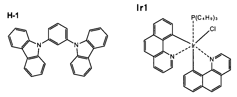
次いで、正孔阻止材料として下記構造式に示すBAlqが入った加熱ボートに通電して加熱し、BAlqよりなる正孔阻止層33を、発光層32上に成膜した。この際、蒸着速度0.1nm/秒~0.2nm/秒、膜厚10nmとした。
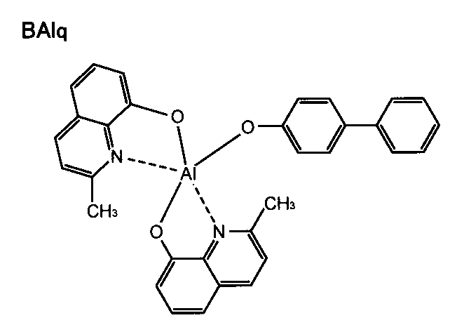
その後、電子輸送材料として、先に窒素含有層を構成する化合物として構造式を示した化合物10の入った加熱ボートと、フッ化カリウムの入った加熱ボートとを、それぞれ独立に通電し、化合物10とフッ化カリウムとからなる電子注入層と電子輸送層とを兼ねた電子輸送・注入層34を、正孔阻止層33上に成膜した。この際、蒸着速度が化合物10:フッ化カリウム=75:25になるように、加熱ボートの通電を調節した。また膜厚30nmとした。
以上の後には、発光機能層3が形成された透明基板13を、真空蒸着装置の第2真空槽内に移送し、第2真空槽内を4×10⁻⁴Paまで減圧した後、第2真空槽内に取り付けられたアルミニウムの入った加熱ボートを通電して加熱した。これにより、蒸着速度0.3nm/秒で膜厚100nmのアルミニウムからなる対向電極5を形成した。この対向電極5は、カソードとして用いられる。以上により透明基板13上に、ボトムエミッション型の有機電界発光素子ELを形成した。
その後、有機電界発光素子ELを、厚さ300μmのガラス基板からなる封止材17で覆い、有機電界発光素子ELを囲む状態で、封止材17と透明基板13との間に接着剤19(シール材)を充填した。接着剤19としては、エポキシ系光硬化型接着剤(東亞合成社製ラックストラックLC0629B)を用いた。封止材17と透明基板13との間に充填した接着剤19に対して、ガラス基板からなる封止材17側からUV光を照射し、接着剤19を硬化させて有機電界発光素子ELを封止した。
試料201~229で作製した有機電界発光素子EL(発光パネル)について、(1)外部量子効率(External Quantum Efficiency:EQE)、(2)高温・高湿保存性の各評価を行った。この結果を下記表3に合わせて示す。
a)発光個数(n/10個)は、各10個の試料201~229のうち、300時間の保存後にも発光が確認された個数であり、10に近いほど好ましい。
b)駆動電圧の変化量ΔVは、各試料201~229において保存後に発光が確認された有機電界発光素子ELの平均値として算出し、数値が小さいほど好ましい。
c)整流比[log]は、保存後の各発光パネルに対して、順方向に+2.5Vの駆動電圧を印加した場合の電流値と、逆方向に-2.5V駆動電圧を印加した場合の電流値を測定し、これらの電流値の比[電流値(+2.5V)/電流値(-2.5V)]の対数値を算出して整流比[log]とした。整流比[log]が高いほどリーク特性に優れていることを表す。この結果を下記表3に合わせて示す。

表3から明らかなように、試料208~229の各有機電界発光素子EL、すなわち高屈折率層、窒素含有層、銀(Ag)を主成分として添加元素を含有する電極層、および高屈折率層がこの順に積層された透明電極を用いた有機電界発光素子ELは、試料201~207と比較して、外部量子効率(EQE)が高く発光特性に優れ、高温高湿環境下での保存後の駆動電圧差が低く、各10個の試料のうちの全てにおいて保存後に発光が確認され、かつ保存後の整流比[log]も十分でリークが抑えられており、高温・高湿耐性にも優れていることが確認された。
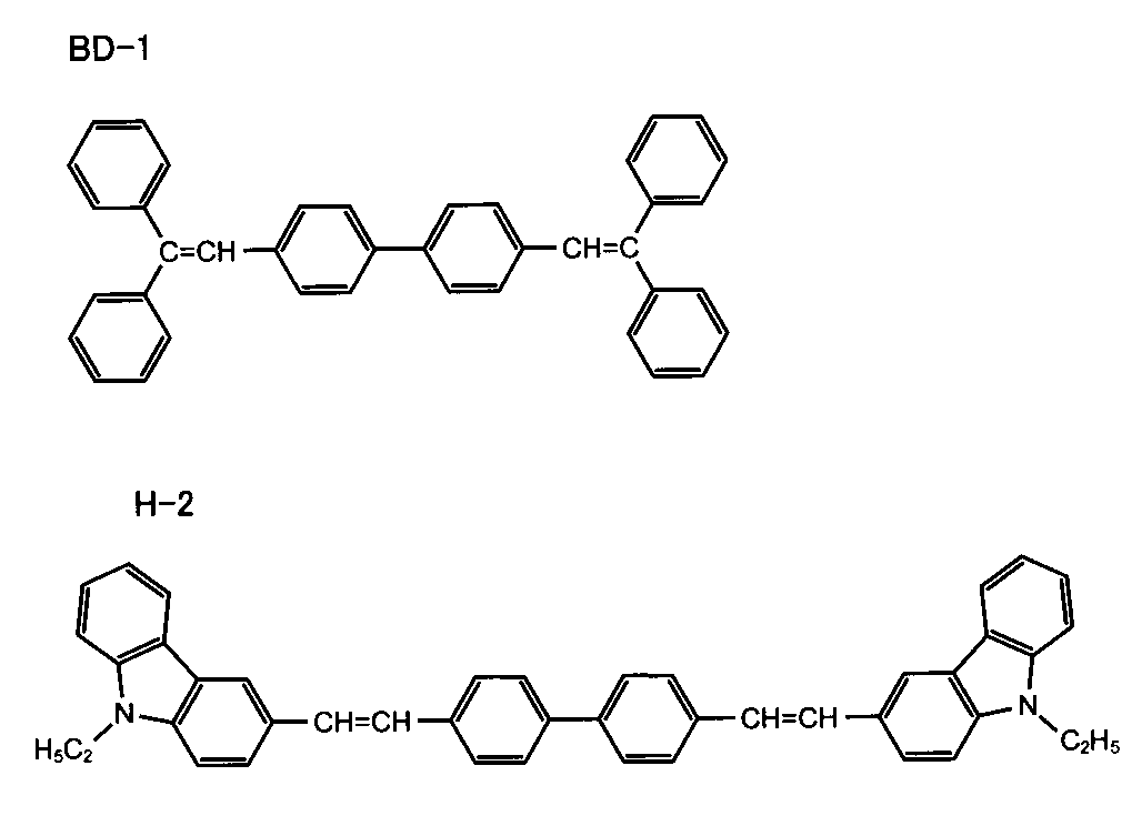
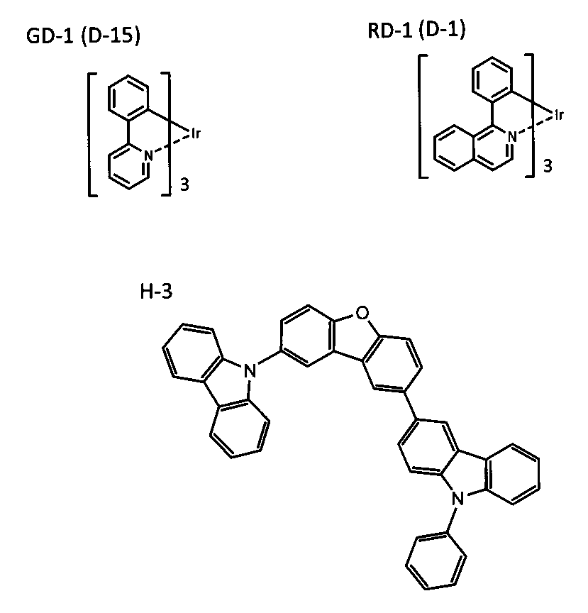
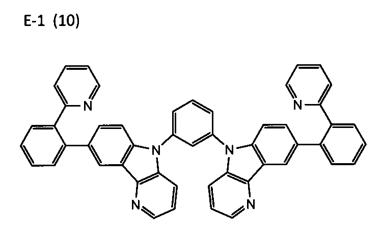
Claims (23)
- 窒素原子(N)を含んだ化合物を用いて構成された窒素含有層と、
前記窒素含有層に隣接して設けられた銀(Ag)を主成分とする電極層と、
前記窒素含有層よりも高い屈折率を有し、前記電極層と前記窒素含有層とを挟持して配置された2つの高屈折率層とを備えた
透明電極。 - 前記化合物は、当該化合物に含まれる窒素原子(N)が有する非共有電子対のうち芳香族性に関与せずかつ金属に配位していない非共有電子対の数をn、分子量をMとした場合の有効非共有電子対含有率[n/M]が、2.0×10-3≦[n/M]となる
請求項1に記載の透明電極。 - 前記化合物における前記有効非共有電子対含有率[n/M]が、3.9×10-3≦[n/M]である
請求項2に記載の透明電極。 - 前記化合物における前記有効非共有電子対含有率[n/M]が、6.5×10-3≦[n/M]である
請求項2に記載の透明電極。 - 前記窒素含有層は、前記電極層側の界面における前記有効非共有電子対含有率[n/M]の値が2.0×10-3≦[n/M]である
請求項2~4の何れかに記載の透明電極。 - 前記高屈折率層は、酸化インジウム、酸化亜鉛、酸化チタン、または酸化ニオブを主成分とする酸化物で構成された
請求項1~5の何れか一項に記載の透明電極。 - 前記窒素含有層は、下記一般式(1)で表される構造を有する化合物を含有する
請求項1~6の何れかに記載の透明電極。

X11は、-N(R11)-または-O-を表し、
E101~E108は、各々-C(R12)=または-N=を表し、E101~E108のうち少なくとも一つは-N=であり、
前記R11および前記R12は、それぞれが水素原子(H)または置換基を表す。] - 前記窒素含有層は、前記一般式(1)におけるX11を-N(R11)-とした下記一般式(1a)で表される構造を有する化合物を含有する
請求項7に記載の透明電極。

- 前記窒素含有層は、前記一般式(1a)におけるE104を-N=とした下記一般式(1a-1)で表される構造を有する化合物を含有する
請求項8に記載の透明電極。
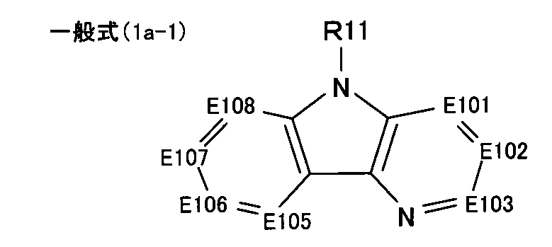
- 前記窒素含有層は、前記一般式(1a)におけるE103およびE106を-N=とした下記一般式(1a-2)で表される構造を有する化合物を含有する
請求項8記載の透明電極。
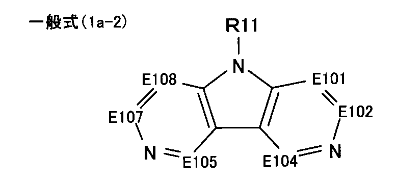
- 前記窒素含有層は、前記一般式(1)におけるX11を-O-とし、E104を-N=とした下記一般式(1b)で表される構造を有する化合物を含有する
請求項7に記載の透明電極。

- 前記窒素含有層は、下記一般式(2)で表される構造を有する化合物を含有する
請求項1~6の何れかに記載の透明電極。

Y21は、アリーレン基、ヘテロアリーレン基またはそれらの組み合わせからなる2価の連結基を表し、
E201~E216、E221~E238は、各々-C(R21)=または-N=を表し、
前記R21は、水素原子(H)または置換基を表し、
E221~E229の少なくとも1つおよびE230~E238の少なくとも1つは-N=であり、
k21およびk22は、0~4の整数を表すが、k21+k22は2以上の整数である。] - 前記窒素含有層は、下記一般式(3)で表される構造を有する化合物を含有する
請求項1~6の何れかに記載の透明電極。
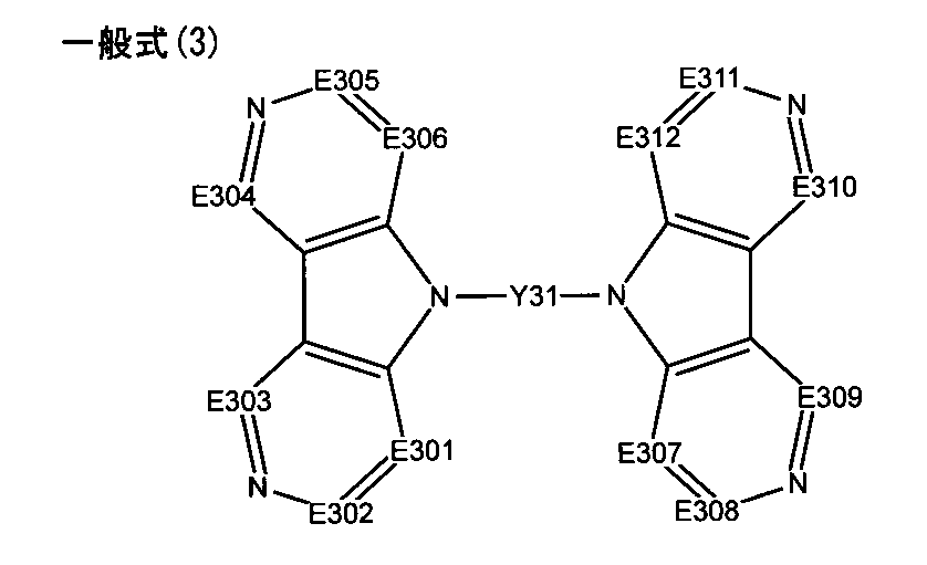
E301~E312は、各々-C(R31)=を表し、
前記R31は水素原子(H)または置換基を表し、
Y31は、アリーレン基、ヘテロアリーレン基またはそれらの組み合わせからなる2価の連結基を表す。] - 前記窒素含有層は、下記一般式(4)で表される構造を有する化合物を含有する
請求項1~6の何れかに記載の透明電極。

E401~E414は、各々-C(R41)=を表し、
前記R41は水素原子(H)または置換基を表し、
Ar41は、置換あるいは無置換の、芳香族炭化水素環あるいは芳香族複素環を表し、
k41は3以上の整数を表す。] - 前記窒素含有層は、下記一般式(5)で表される構造を有する化合物を含有する
請求項1~6の何れかに記載の透明電極。
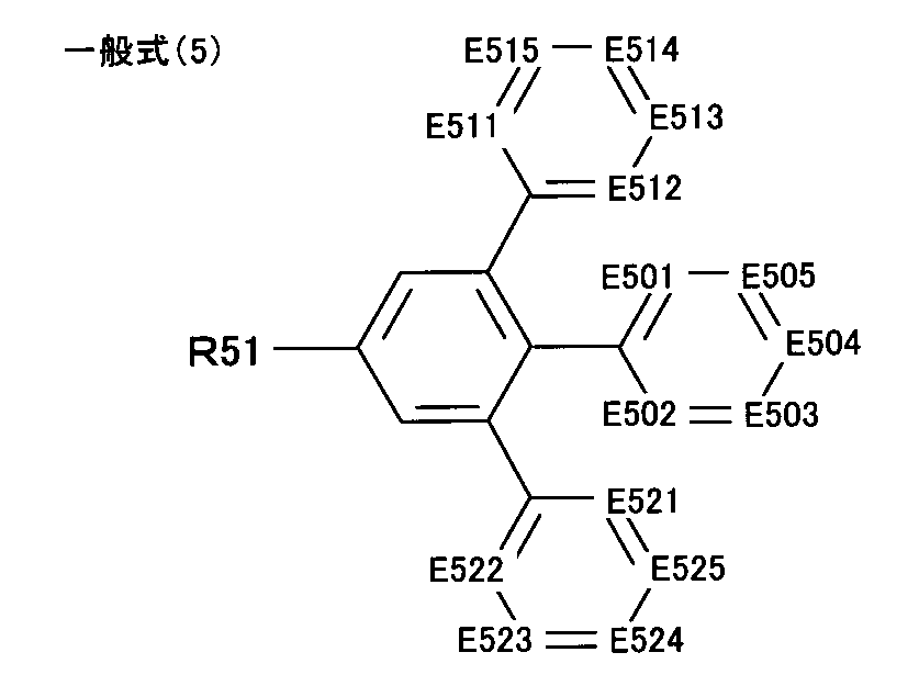
R51は置換基を表し、
E501,E502、E511~E515、E521~E525は、各々-C(R52)=または-N=を表し、
E503~E505は、各々-C(R52)=を表し、
前記R52は、水素原子(H)または置換基を表し、
E501およびE502のうち少なくとも1つは-N=であり、
E511~E515のうち少なくとも1つは-N=であり、
E521~E525のうち少なくとも1つは-N=である。] - 前記窒素含有層は、下記一般式(6)で表される構造を有する化合物を含有する
請求項1~6の何れかに記載の透明電極。
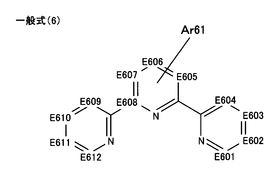
E601~E612は、各々-C(R61)=または-N=を表し、
前記R61は水素原子(H)または置換基を表し、
Ar61は、置換あるいは無置換の、芳香族炭化水素環あるいは芳香族複素環を表す。] - 前記窒素含有層は、下記一般式(7)で表される構造を有する化合物を含有する
請求項1~6のいずれか一項に記載の透明電極。
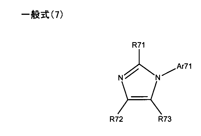
R71~R73は、各々水素原子(H)または置換基を表し、
Ar71は、芳香族炭化水素環基あるいは芳香族複素環基を表す。〕 - 前記窒素含有層は、下記一般式(8)で表される構造を有する化合物を含有する
請求項1~6のいずれか一項に記載の透明電極。
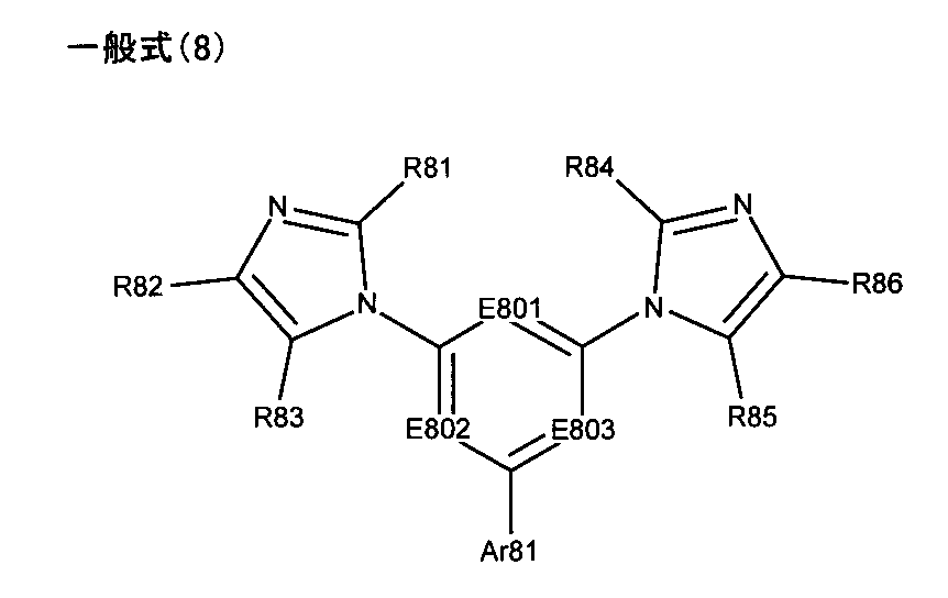
R81~R86は、各々水素原子(H)または置換基を表し、
E801~E803は、各々-C(R87)=または-N=を表し、
前記R87は、水素原子(H)または置換基を表し、
Ar81は、芳香族炭化水素環基または芳香族複素環基を表す。〕 - 前記窒素含有層は、下記一般式(8a)で表される構造を有する化合物を含有する
請求項18に記載の透明電極。

E804~E811は、各々-C(R88)=または-N=を表し、
前記R88は、それぞれが水素原子(H)または置換基と表し、
E808~E811のうち少なくとも一つは-N=であり、
E804~E807、E808~E811は、各々互いに結合して新たな環を形成してもよい。〕 - 請求項1~19の何れかに記載の透明電極を有する
電子デバイス。 - 前記電子デバイスが有機電界発光素子である
請求項20に記載の電子デバイス。 - 請求項1~19の何れかに記載の透明電極と、
前記透明電極に積層して設けられた発光機能層と、
前記透明電極との間に前記発光機能層を挟持する状態で設けられた対向電極とを有する
有機電界発光素子。 - 前記発光機能層は、前記窒素含有層との間に前記電極層を挟持する位置に設けられた
請求項22記載の有機電界発光素子。
Priority Applications (3)
| Application Number | Priority Date | Filing Date | Title |
|---|---|---|---|
| CN201480004457.8A CN104919899B (zh) | 2013-01-15 | 2014-01-08 | 透明电极、电子器件、及有机电致发光元件 |
| JP2014557426A JP6314838B2 (ja) | 2013-01-15 | 2014-01-08 | 透明電極、電子デバイス、および有機電界発光素子 |
| US14/760,354 US9917263B2 (en) | 2013-01-15 | 2014-01-08 | Transparent electrode, electronic device, and organic electroluminescent element |
Applications Claiming Priority (2)
| Application Number | Priority Date | Filing Date | Title |
|---|---|---|---|
| JP2013-004795 | 2013-01-15 | ||
| JP2013004795 | 2013-01-15 |
Publications (1)
| Publication Number | Publication Date |
|---|---|
| WO2014112410A1 true WO2014112410A1 (ja) | 2014-07-24 |
Family
ID=51209502
Family Applications (1)
| Application Number | Title | Priority Date | Filing Date |
|---|---|---|---|
| PCT/JP2014/050118 Ceased WO2014112410A1 (ja) | 2013-01-15 | 2014-01-08 | 透明電極、電子デバイス、および有機電界発光素子 |
Country Status (4)
| Country | Link |
|---|---|
| US (1) | US9917263B2 (ja) |
| JP (1) | JP6314838B2 (ja) |
| CN (1) | CN104919899B (ja) |
| WO (1) | WO2014112410A1 (ja) |
Cited By (1)
| Publication number | Priority date | Publication date | Assignee | Title |
|---|---|---|---|---|
| CN107278384A (zh) * | 2015-02-27 | 2017-10-20 | 柯尼卡美能达株式会社 | 透明电极及电子器件 |
Families Citing this family (5)
| Publication number | Priority date | Publication date | Assignee | Title |
|---|---|---|---|---|
| KR101997661B1 (ko) * | 2015-10-27 | 2019-07-08 | 주식회사 엘지화학 | 전도성 구조체, 이를 포함하는 전극 및 디스플레이 장치 |
| CN109273613A (zh) * | 2017-07-17 | 2019-01-25 | 昆山国显光电有限公司 | Oled器件及其制备方法、显示装置 |
| JP6852172B2 (ja) * | 2017-09-19 | 2021-03-31 | 株式会社日本触媒 | 有機電界発光素子 |
| US11426818B2 (en) | 2018-08-10 | 2022-08-30 | The Research Foundation for the State University | Additive manufacturing processes and additively manufactured products |
| KR102245143B1 (ko) | 2019-12-03 | 2021-04-28 | 경희대학교 산학협력단 | 투명전극 및 이를 이용하는 유기 전자 소자 |
Citations (7)
| Publication number | Priority date | Publication date | Assignee | Title |
|---|---|---|---|---|
| JP2002110365A (ja) * | 2000-10-04 | 2002-04-12 | Idemitsu Kosan Co Ltd | 有機エレクトロルミネッセンス表示素子用透明電極基板および有機エレクトロルミネッセンス表示素子 |
| JP2002313139A (ja) * | 2001-04-12 | 2002-10-25 | Mitsui Chemicals Inc | 透明導電性薄膜積層体 |
| JP2005044790A (ja) * | 2003-07-08 | 2005-02-17 | Konica Minolta Holdings Inc | 有機エレクトロルミネッセンス素子、照明装置および表示装置 |
| WO2009054253A1 (ja) * | 2007-10-26 | 2009-04-30 | Konica Minolta Holdings, Inc. | 有機エレクトロルミネッセンス素子、表示装置及び照明装置 |
| JP2010251675A (ja) * | 2008-05-13 | 2010-11-04 | Konica Minolta Holdings Inc | 有機エレクトロルミネッセンス素子、表示装置及び照明装置 |
| WO2011004807A1 (ja) * | 2009-07-10 | 2011-01-13 | コニカミノルタホールディングス株式会社 | 有機光電変換素子、それを用いた太陽電池および光センサアレイ |
| JP2011077028A (ja) * | 2009-09-04 | 2011-04-14 | Hitachi Displays Ltd | 有機el表示装置 |
Family Cites Families (5)
| Publication number | Priority date | Publication date | Assignee | Title |
|---|---|---|---|---|
| JP2002015623A (ja) | 2000-04-27 | 2002-01-18 | Mitsui Chemicals Inc | 透明電極 |
| CN1767223A (zh) * | 2004-10-28 | 2006-05-03 | 国联光电科技股份有限公司 | 半导体发光组件及其制造方法 |
| JP2006164961A (ja) | 2004-11-09 | 2006-06-22 | Ulvac Seimaku Kk | 積層型透明電極層の製造方法及びこの方法に使用する積層型透明電極形成用の積層体 |
| JP2008171637A (ja) | 2007-01-10 | 2008-07-24 | Fuji Electric Holdings Co Ltd | 透明導電膜積層体、該透明導電膜積層体を用いた有機el素子、並びに、これらの製造方法 |
| JP2009151963A (ja) | 2007-12-19 | 2009-07-09 | Institute Of Physical & Chemical Research | 透明電極およびその製造方法 |
-
2014
- 2014-01-08 CN CN201480004457.8A patent/CN104919899B/zh not_active Expired - Fee Related
- 2014-01-08 US US14/760,354 patent/US9917263B2/en not_active Expired - Fee Related
- 2014-01-08 WO PCT/JP2014/050118 patent/WO2014112410A1/ja not_active Ceased
- 2014-01-08 JP JP2014557426A patent/JP6314838B2/ja not_active Expired - Fee Related
Patent Citations (7)
| Publication number | Priority date | Publication date | Assignee | Title |
|---|---|---|---|---|
| JP2002110365A (ja) * | 2000-10-04 | 2002-04-12 | Idemitsu Kosan Co Ltd | 有機エレクトロルミネッセンス表示素子用透明電極基板および有機エレクトロルミネッセンス表示素子 |
| JP2002313139A (ja) * | 2001-04-12 | 2002-10-25 | Mitsui Chemicals Inc | 透明導電性薄膜積層体 |
| JP2005044790A (ja) * | 2003-07-08 | 2005-02-17 | Konica Minolta Holdings Inc | 有機エレクトロルミネッセンス素子、照明装置および表示装置 |
| WO2009054253A1 (ja) * | 2007-10-26 | 2009-04-30 | Konica Minolta Holdings, Inc. | 有機エレクトロルミネッセンス素子、表示装置及び照明装置 |
| JP2010251675A (ja) * | 2008-05-13 | 2010-11-04 | Konica Minolta Holdings Inc | 有機エレクトロルミネッセンス素子、表示装置及び照明装置 |
| WO2011004807A1 (ja) * | 2009-07-10 | 2011-01-13 | コニカミノルタホールディングス株式会社 | 有機光電変換素子、それを用いた太陽電池および光センサアレイ |
| JP2011077028A (ja) * | 2009-09-04 | 2011-04-14 | Hitachi Displays Ltd | 有機el表示装置 |
Cited By (2)
| Publication number | Priority date | Publication date | Assignee | Title |
|---|---|---|---|---|
| CN107278384A (zh) * | 2015-02-27 | 2017-10-20 | 柯尼卡美能达株式会社 | 透明电极及电子器件 |
| CN107278384B (zh) * | 2015-02-27 | 2020-09-25 | 柯尼卡美能达株式会社 | 透明电极及电子器件 |
Also Published As
| Publication number | Publication date |
|---|---|
| US9917263B2 (en) | 2018-03-13 |
| US20150357581A1 (en) | 2015-12-10 |
| JP6314838B2 (ja) | 2018-04-25 |
| JPWO2014112410A1 (ja) | 2017-01-19 |
| CN104919899A (zh) | 2015-09-16 |
| CN104919899B (zh) | 2017-07-11 |
Similar Documents
| Publication | Publication Date | Title |
|---|---|---|
| JP6802189B2 (ja) | 薄膜、及び有機エレクトロルミネッセンス素子 | |
| JP6128117B2 (ja) | 透明電極の製造方法 | |
| JP6287854B2 (ja) | 透明電極、電子デバイス、および有機電界発光素子 | |
| CN103946020A (zh) | 透明电极及电子器件 | |
| JP5943005B2 (ja) | 透明電極、電子デバイス、有機電界発光素子、および有機電界発光素子の製造方法 | |
| JP6217642B2 (ja) | 透明電極、電子デバイス、および透明電極の製造方法 | |
| JP6256349B2 (ja) | 透明電極、及び、電子デバイス | |
| JP6314838B2 (ja) | 透明電極、電子デバイス、および有機電界発光素子 | |
| JP6304229B2 (ja) | 透明電極、電子デバイス、および有機電界発光素子 | |
| JP6241189B2 (ja) | 透明電極、透明電極の製造方法、電子デバイス及び有機エレクトロルミネッセンス素子 | |
| JP6112107B2 (ja) | 透明電極、電子デバイス及び有機エレクトロルミネッセンス素子 | |
| JP2015060728A (ja) | 透明電極、及び、有機エレクトロルミネッセンス素子 | |
| JP6241281B2 (ja) | 透明電極および電子デバイス | |
| JP6070320B2 (ja) | 透明電極付き基板、及び、電子デバイス | |
| JPWO2015125581A1 (ja) | 有機電界発光素子 | |
| JP6314839B2 (ja) | 透明電極、電子デバイス、および有機電界発光素子 | |
| JPWO2014181640A1 (ja) | 発光素子および表示装置 | |
| JPWO2014098014A1 (ja) | 透明電極、及び、電子デバイス | |
| JPWO2014175181A1 (ja) | 透明導電体、及び、電子デバイス | |
| JPWO2014175451A1 (ja) | 透明導電体、及び、電子デバイス |
Legal Events
| Date | Code | Title | Description |
|---|---|---|---|
| 121 | Ep: the epo has been informed by wipo that ep was designated in this application |
Ref document number: 14740874 Country of ref document: EP Kind code of ref document: A1 |
|
| ENP | Entry into the national phase |
Ref document number: 2014557426 Country of ref document: JP Kind code of ref document: A |
|
| WWE | Wipo information: entry into national phase |
Ref document number: 14760354 Country of ref document: US |
|
| NENP | Non-entry into the national phase |
Ref country code: DE |
|
| 122 | Ep: pct application non-entry in european phase |
Ref document number: 14740874 Country of ref document: EP Kind code of ref document: A1 |