WO2014109097A1 - ヒューズ - Google Patents
ヒューズ Download PDFInfo
- Publication number
- WO2014109097A1 WO2014109097A1 PCT/JP2013/075862 JP2013075862W WO2014109097A1 WO 2014109097 A1 WO2014109097 A1 WO 2014109097A1 JP 2013075862 W JP2013075862 W JP 2013075862W WO 2014109097 A1 WO2014109097 A1 WO 2014109097A1
- Authority
- WO
- WIPO (PCT)
- Prior art keywords
- melting point
- fuse
- wiring
- low melting
- point metal
- Prior art date
- Legal status (The legal status is an assumption and is not a legal conclusion. Google has not performed a legal analysis and makes no representation as to the accuracy of the status listed.)
- Ceased
Links
Images





Classifications
-
- H—ELECTRICITY
- H01—ELECTRIC ELEMENTS
- H01H—ELECTRIC SWITCHES; RELAYS; SELECTORS; EMERGENCY PROTECTIVE DEVICES
- H01H85/00—Protective devices in which the current flows through a part of fusible material and this current is interrupted by displacement of the fusible material when this current becomes excessive
- H01H85/02—Details
- H01H85/04—Fuses, i.e. expendable parts of the protective device, e.g. cartridges
- H01H85/041—Fuses, i.e. expendable parts of the protective device, e.g. cartridges characterised by the type
- H01H85/044—General constructions or structure of low voltage fuses, i.e. below 1000 V, or of fuses where the applicable voltage is not specified
- H01H85/045—General constructions or structure of low voltage fuses, i.e. below 1000 V, or of fuses where the applicable voltage is not specified cartridge type
-
- H—ELECTRICITY
- H01—ELECTRIC ELEMENTS
- H01H—ELECTRIC SWITCHES; RELAYS; SELECTORS; EMERGENCY PROTECTIVE DEVICES
- H01H85/00—Protective devices in which the current flows through a part of fusible material and this current is interrupted by displacement of the fusible material when this current becomes excessive
- H01H85/0039—Means for influencing the rupture process of the fusible element
- H01H85/0047—Heating means
- H01H85/0056—Heat conducting or heat absorbing means associated with the fusible member, e.g. for providing time delay
-
- H—ELECTRICITY
- H01—ELECTRIC ELEMENTS
- H01H—ELECTRIC SWITCHES; RELAYS; SELECTORS; EMERGENCY PROTECTIVE DEVICES
- H01H85/00—Protective devices in which the current flows through a part of fusible material and this current is interrupted by displacement of the fusible material when this current becomes excessive
- H01H85/0039—Means for influencing the rupture process of the fusible element
- H01H85/0047—Heating means
- H01H85/006—Heat reflective or insulating layer on the casing or on the fuse support
-
- H—ELECTRICITY
- H01—ELECTRIC ELEMENTS
- H01H—ELECTRIC SWITCHES; RELAYS; SELECTORS; EMERGENCY PROTECTIVE DEVICES
- H01H85/00—Protective devices in which the current flows through a part of fusible material and this current is interrupted by displacement of the fusible material when this current becomes excessive
- H01H85/0039—Means for influencing the rupture process of the fusible element
- H01H85/0047—Heating means
- H01H85/0065—Heat reflective or insulating layer on the fusible element
-
- H—ELECTRICITY
- H01—ELECTRIC ELEMENTS
- H01H—ELECTRIC SWITCHES; RELAYS; SELECTORS; EMERGENCY PROTECTIVE DEVICES
- H01H85/00—Protective devices in which the current flows through a part of fusible material and this current is interrupted by displacement of the fusible material when this current becomes excessive
- H01H85/02—Details
- H01H85/04—Fuses, i.e. expendable parts of the protective device, e.g. cartridges
- H01H85/05—Component parts thereof
- H01H85/055—Fusible members
- H01H85/08—Fusible members characterised by the shape or form of the fusible member
- H01H85/11—Fusible members characterised by the shape or form of the fusible member with applied local area of a metal which, on melting, forms a eutectic with the main material of the fusible member, i.e. M-effect devices
-
- H—ELECTRICITY
- H01—ELECTRIC ELEMENTS
- H01H—ELECTRIC SWITCHES; RELAYS; SELECTORS; EMERGENCY PROTECTIVE DEVICES
- H01H85/00—Protective devices in which the current flows through a part of fusible material and this current is interrupted by displacement of the fusible material when this current becomes excessive
- H01H85/48—Protective devices wherein the fuse is carried or held directly by the base
Definitions
- the present invention relates to a fuse.
- Patent Document 1 As an example of a fuse, first and second electrode portions disposed on an insulating substrate, a metal wiring portion that connects the first electrode portion and the second electrode portion, and A fuse including a low melting point metal part disposed on a part of a metal wiring part is described.
- An object of the present invention is to provide a fuse capable of reliably interrupting an overcurrent.
- the fuse according to the present invention includes an insulating substrate, a wiring, a low melting point metal part, an insulating layer, and a metal film.
- the wiring is arranged on one main surface of the insulating substrate.
- the low melting point metal part is provided on the wiring.
- the low melting point metal part has a melting point lower than that of the wiring, and dissolves the wiring when it becomes a melt.
- the insulating layer is disposed between the wiring and the low melting point metal part.
- the metal film is disposed outside the insulating layer on the insulating substrate.
- the low melting point metal part is provided in contact with the metal film.
- metal films are provided on both sides of the insulating layer in the width direction of the wiring.
- the low melting point metal portion is provided so as to extend from one of the two metal films to the other.
- the fuse connects the low melting point metal part and the metal film, has a higher melting point than the low melting point metal part, and has a lower melting point than the metal film.
- the unit is further provided.
- the melting point of the insulating layer is higher than the melting point of the low melting point metal part.
- the insulating layer is made of a thermoplastic resin.
- the fuse further includes a heating element for heating the low melting point metal part.
- the low-melting point metal portion is mainly composed of Sn.
- FIG. 1 is a schematic plan view of a fuse in an embodiment of the present invention.
- FIG. 2 is a schematic back view of a fuse in one embodiment of the present invention.
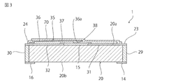
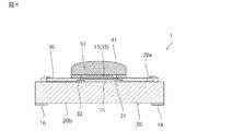
- 3 is a schematic cross-sectional view taken along line III-III in FIG. 4 is a schematic cross-sectional view taken along line IV-IV in FIG.
- FIG. 5 is a schematic cross-sectional view taken along line VV in FIG.
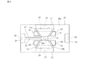
- FIG. 6 is a schematic plan view for explaining the shape of the second electrode layer in one embodiment of the present invention.
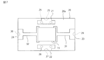
- FIG. 7 is a schematic plan view for explaining the shapes of the first electrode layer and the heating element in one embodiment of the present invention.
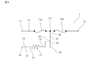
- FIG. 8 is a schematic circuit diagram of a fuse in one embodiment of the present invention.
- FIG. 9 is a schematic cross-sectional view of a fuse in the first modification.
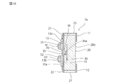
- FIG. 10 is a schematic cross-sectional view of a fuse in the second modification.
- FIG. 11 is a schematic cross-sectional view of a fuse in
- FIG. 1 is a schematic plan view of a fuse in the present embodiment.
- FIG. 2 is a schematic rear view of the fuse in the present embodiment.
- 3 is a schematic cross-sectional view taken along line III-III in FIG. 4 is a schematic cross-sectional view taken along line IV-IV in FIG.
- FIG. 5 is a schematic cross-sectional view taken along line VV in FIG.
- FIG. 6 is a schematic plan view for explaining the shape of the second electrode layer in the present embodiment.
- FIG. 7 is a schematic plan view for explaining the shapes of the first electrode layer and the heating element in the present embodiment.
- FIG. 8 is a schematic circuit diagram of the fuse in the present embodiment. In FIG. 6 and FIG. 7, drawing of members located on the members to be explained is omitted.
- the fuse 1 has a wiring 13 connected between a first terminal 11 and a second terminal 12.
- fuse electrode portions 13a and 13b are connected in series.
- the fuse electrode portions 13a and 13b are blown when an overcurrent flows through the fuse 1 or when a signal for causing the fuse function to be developed is input to the fuse 1, and the first terminal 11 and the second terminal 12 is an insulating part.
- the fuse electrode portions 13a and 13b is melted.
- the 1st terminal 11 and the 2nd terminal 12 are insulated. Therefore, the fuse 1 functions as a passive element that detects an overcurrent and automatically disconnects the wiring 13.
- the thickness of the wiring 13 can be set to about 5 ⁇ m to 20 ⁇ m, for example.
- connection point 13 c between the fuse electrode portion 13 a and the fuse electrode portion 13 b is connected to the fourth terminal 16.
- a heating element 15 made of a resistor is provided between the third terminal 14 and the connection point 13c.
- the heating element 15 generates heat when electric power is applied between the third terminal 14 and at least one of the first and second terminals 11 and 12. Thereby, at least one of the fuse electrode portion 13a and the fuse electrode portion 13b is melted, and the first terminal 11 and the second terminal 12 are insulated. Therefore, the fuse 1 also functions as an active element that detects an overcurrent and actively cuts the wiring 13.
- the fuse according to the present invention may function only as a passive element or may function only as an active element.
- the fuse 1 includes an insulating substrate 20.
- the insulating substrate 20 can be configured by a ceramic substrate such as an alumina substrate, a resin substrate, or the like, for example.
- the insulating substrate 20 may be a multilayer substrate having wiring inside.
- the insulating substrate 20 has a first main surface 20a and a second main surface 20b. As shown in FIG. 2, the first to fourth terminals 11, 12, 14, and 16 are disposed on the second main surface 20b. The fourth terminal 16 is connected to a connection point between the heating element 15 and the connection point 13c shown in FIG.
- the first to fourth terminals 11, 12, 14, and 16 can be made of an appropriate conductive material such as Ag, AgPt, AgPd, or Cu.
- the thickness of the first to fourth terminals 11, 12, 14, and 16 can be, for example, about 10 ⁇ m to 20 ⁇ m.
- electrodes 21 to 24 are provided on the first main surface 20a.
- the electrode 21 is connected to the first terminal 11 by a side electrode 25 and a via hole electrode 26 (see FIG. 2).
- the electrode 22 is connected to the second terminal 12 by a side electrode 27 and a via hole electrode 28.
- the electrode 23 is connected to the third terminal 14 by a side electrode 29.
- the electrode 24 is connected to the fourth terminal 16 by a side electrode 30.
- Each of the electrodes 21 to 24 can be made of an appropriate conductive material such as Ag, AgPt, AgPd, or Cu.
- the heating element 15 connected between the electrode 23 and the electrode 24 is provided on the main surface 20 a.
- the electrode 23 and the heating element 15 are connected by a wiring 31.
- the electrode 24 and the heating element 15 are connected by a wiring 32.
- the heating element 15 is supported by the insulating substrate 20.
- the heating element 15, for example, can be constituted by a resistive heating element consisting of RuO 2, AgPd, or the like.
- An electrode layer 35 (see FIGS. 3 to 6) is provided on the electrodes 23 and 24, the heating element 15, and the wirings 31 and 32.
- An insulating layer 36 is disposed between the electrode layer 35 and the electrodes 23 and 24 and the wirings 31 and 32.
- the insulating layer 36 is provided on the entire portion where the wirings 31 and 32 and the low melting point metal parts 41 and 42 overlap.
- an opening or the like is formed in the insulating layer, and the wiring and the low melting point metal part may be connected to such an extent that the electrical resistance of the wiring does not decrease too much as a whole.
- the insulating layer 36 is provided with a through hole 36 a.
- the through hole 36a is connected to each of the heating element 15 and the wiring 13 (specifically, the connection point 13c).
- the through hole 36a may be provided with a substantially constant diameter in the direction in which the central axis extends, or may be provided in a tapered shape.
- the through hole 36a may be provided in a tapered shape that tapers toward the insulating substrate 20 side, for example.
- the thickness of the insulating layer 36 can be set to about 15 ⁇ m to 30 ⁇ m, for example.
- the electrode layer 35 includes a wiring 13 that connects the electrode 21 and the electrode 22.
- the wiring 13 includes a fuse electrode portion 13a and a fuse electrode portion 13b.
- a connection point 13c between the fuse electrode portion 13a and the fuse electrode portion 13b and the electrode 24 are connected by an electrode 37 shown in FIGS.
- the connection point 13c is connected to the heating element 15 through a high thermal conductor 38 disposed in the through hole 36a.
- the thermal conductivity of the high thermal conductor 38 is higher than the thermal conductivity of the insulating layer 36.
- the high thermal conductor 38 can be made of, for example, a metal.
- the high thermal conductor 38 and the wiring 13 are integrally provided. In this case, the high thermal conductor 38 can be easily provided.
- the thickness of the electrode layer 35 can be set to about 5 ⁇ m to 20 ⁇ m, for example.
- low melting point metal parts 41 and 42 are provided on the fuse electrode parts 13a and 13b of the wiring 13, respectively.
- the low melting point metal parts 41 and 42 are made of a low melting point metal that has a melting point lower than that of the wiring 13 and that melts the wiring 13 when it becomes a melt.
- the low melting point metal may be composed mainly of Sn, for example. Specific examples of such low melting point metals include Sn alloys such as SnSb, SnCu, SnAg, SnAgCu, SnCuNi.
- the thickness of the low melting point metal parts 41, 42 can be set to about 0.1 mm to 0.5 mm, for example.
- a protective film such as a flux layer, an antioxidant film, or the like may be provided on the low melting point metal parts 41 and 42 so as to cover at least a part of the low melting point metal parts 41 and 42.
- insulating layers 51 and 52 are arranged between the wiring 13 and the low melting point metal portions 41 and 42.
- the melting points of the insulating layers 51 and 52 are higher than the melting points of the low melting point metal parts 41 and 42.
- the melting points of the insulating layers 51 and 52 are preferably 180 ° C. to 350 ° C., and more preferably 220 ° C. to 320 ° C.
- the insulating layers 51 and 52 can be made of an appropriate insulating material, but are preferably made of, for example, a thermoplastic resin.
- thermoplastic resin preferably used for forming the insulating layers 51 and 52 examples include polyester resins such as polyethylene terephthalate (PET, melting point 264 ° C.), polybutylene terephthalate (PBT, melting point 232 ° C.), and polyvinyl chloride.
- PET polyethylene terephthalate
- PBT polybutylene terephthalate
- polyvinyl chloride examples include polyvinyl chloride.
- the thickness of the insulating layers 51 and 52 can be, for example, about 10 ⁇ m to 200 ⁇ m, preferably about 20 to 150 ⁇ m.
- metal films 61 to 64 are disposed outside the insulating layers 51 and 52.
- the metal films 61 to 64 are preferably made of, for example, a metal or alloy having high wettability to the melt of the low melting point metal parts 41 and 42 such as Ag, AgPt, AgPd, and Cu.
- the metal films 61 to 64 are preferably not easily dissolved in the melt of the low melting point metal parts 41 and 42, and are particularly preferably composed of AgPt, AgPd, or the like.
- the metal films 61 to 64 are provided on both sides of the insulating layers 51 and 52 in the width direction of the wiring 13.
- the metal films 61 and 62 are provided on both sides of the insulating layer 51 in the width direction of the wiring 13.
- the metal films 61 and 62 are provided so as to sandwich the fuse electrode portion 13a.
- the low melting point metal part 41 is provided in contact with the metal films 61 and 62.
- the low melting point metal portion 41 is provided so as to straddle the insulating layer 51 and the metal film 62 from the top of the metal film 61.
- Metal films 63 and 64 are provided on both sides of the insulating layer 52 in the width direction of the wiring 13. In the width direction of the wiring 13, the metal films 63 and 64 are provided so as to sandwich the fuse electrode portion 13b.
- the low melting point metal part 42 is provided in contact with the metal films 63 and 64. Specifically, the low melting point metal part 42 is provided over the metal film 63, the insulating layer 52, and the metal film 64.
- the metal films 61 to 64 may be formed of a laminate of a plurality of metal films.
- the plurality of metal films constituting the metal films 61 to 64 may include a plurality of types of metal films having different melting points.
- the metal films 61 to 64 are provided on the first metal film and the first metal film, and may include a second metal film having a melting point lower than that of the first metal film. In that case, the second metal film may reach the insulating layers 51 and 52.
- the thickness of the metal films 61 to 64 can be set to about 20 ⁇ m to 40 ⁇ m, for example.
- a protective layer 70 surrounding each of the region provided with the low melting point metal part 41 and the region provided with the low melting point metal part 42 is provided.
- the thickness of the protective layer 70 can be, for example, about 10 ⁇ m to 20 ⁇ m.
- the fuse electrode portions 13a and 13b provided narrowly generate heat. Due to this heat generation, the low melting point metal parts 41 and 42 are heated and melted. Further, the insulating layers 51 and 52 are also melted, and the low melting point metal melt comes into contact with the fuse electrode portions 13a and 13b. As a result, the fuse electrode portions 13a and 13b are dissolved in the melt of the low melting point metal, and the wiring 13 is melted. As a result, a fuse function appears.
- insulating layers 51 and 52 are provided between the wiring 13 and the low melting point metal parts 41 and 42.
- the insulating layer 51, 52 electrically insulates the wiring 13 from the low melting point metal parts 41, 42.
- the specific resistance of the wiring 13 is large. Therefore, the wiring 13 tends to generate heat when an overcurrent flows between the first terminal 11 and the second terminal 12. Therefore, in the fuse 1, when an overcurrent flows between the first terminal 11 and the second terminal 12, the fuse function appears with high certainty.
- the melting points of the insulating layers 51 and 52 are higher than the melting points of the low melting point metal parts 41 and 42. For this reason, it is suppressed effectively that the specific resistance of the wiring 13 falls because the low melting-point metal parts 41 and 42 and the wiring 13 contact until the insulating layers 51 and 52 melt
- the melting points of the insulating layers 51 and 52 are preferably higher by 10 ° C. than the melting points of the low melting point metal parts 41 and 42, and more preferably higher by 20 ° C. or more.
- the melting points of the insulating layers 51 and 52 are too high relative to the melting points of the low melting point metal parts 41 and 42, the insulating layers 51 and 52 are difficult to melt, and the low melting point metal melt and the wiring 13 are difficult to contact.
- the fuse function may be difficult to develop.
- the melting points of the insulating layers 51 and 52 are preferably not higher than the melting point of the low melting point metal portions 41 and 42 + 50 ° C., more preferably not higher than the melting point of the low melting point metal portions 41 and 42 + 30 ° C.
- the melting points of the insulating layers 51 and 52 are preferably within a range of 180 ° C. to 350 ° C., more preferably within a range of 220 ° C. to 320 ° C., and a range of 260 ° C. to 280 ° C. More preferably, it is within.
- the fuse 1 metal films 61 to 64 are disposed on the insulating substrate 20 outside the insulating layers 51 and 52.
- the low melting point metal melt contacts the metal films 61 to 64, the low melting point metal melt is captured by the metal films 61 to 64. Therefore, in the fuse 1, it is possible to reliably keep the melt of the low melting point metal in a region where it can come into contact with the wiring 13. Therefore, in the fuse 1, the fuse function can be expressed with high certainty.
- the low melting point metal portions 41 and 42 are preferably provided so as to be in contact with the metal films 61 to 64.
- the metal films 61 to 64 are preferably provided on both sides of the insulating layers 51 and 52 in the width direction of the wiring 13. In the width direction of the wiring 13, the metal films 61 to 64 are preferably provided on both sides of the fuse electrode portions 13a and 13b.
- the low melting point metal parts 41 and 42 are preferably provided across the metal film 61 and the metal film 62, and the metal film 63 and the metal film 64 provided on both sides of the wiring 13.
- the fuse function can be exhibited by causing the heating element 15 to generate heat.
- the heating element 15 is caused to generate heat by applying electric power between the third terminal 14 and the terminals 11, 12 or 16. Due to the heat from the heating element 15, the low melting point metal parts 41 and 42 are melted and the fuse electrode parts 13 a and 13 b of the wiring 13 are melted.
- the heating element 15 and the wiring 13 are connected by a high thermal conductor 38 that is provided in the through hole 36 a and has a higher thermal conductivity than the insulating layer 36. For this reason, the heat of the heating element 15 is easily transmitted to the low melting point metal parts 41 and 42 via the wiring 13. Therefore, in the fuse 1, the fuse function is expressed with high certainty even when the heating element 15 is heated to actively develop the fuse function.
- the through hole 36a is provided so as not to overlap the low melting point metal parts 41 and 42 in a plan view.
- the high thermal conductor 38 is conductive in order to melt the wiring 13 and insulate the first terminal 11 and the second terminal 12 from each other. In the case where it has the property, it is necessary to blow up to the high thermal conductor 38 together with the wiring 13.
- the through hole 36a is provided so as not to overlap the low melting point metal parts 41 and 42, the first terminal 11 and the second terminal 12 are insulated if only the wiring 13 is melted. Is done. Accordingly, the fuse function is more easily exhibited.
- FIG. 9 is a schematic cross-sectional view of a fuse in the first modification.
- the fuse 1 a covers the low melting point metal parts 41 and 42, and may further include an insulating layer 80 having a melting point higher than that of the low melting point metal parts 41 and 42.
- an insulating layer 80 By providing this insulating layer 80, it is possible to prevent the low melting point metal portions 41 and 42 from being melted and spreading in the unintended direction of the low melting point metal melt.
- the melting point of the insulating layer 80 is preferably higher than the melting point of the low melting point metal parts 41, 42 by 10 ° C. or more, more preferably 20 ° C. or more.
- the insulating layer 80 can be made of an insulating material that can be used for the insulating layers 51 and 52, such as polyethylene terephthalate, polybutylene terephthalate, and polycarbonate.
- FIG. 10 is a schematic cross-sectional view of a fuse in the second modification.
- the heating element 15 is provided on the insulating substrate 20 in the fuse 1 according to the above embodiment.
- the present invention is not limited to this configuration.
- the heating element 15 is provided inside the insulating substrate 20 in the fuse 1 b according to this modification.
- a portion located between the heating element 15 and the wiring 13 of the insulating substrate 20 constitutes an insulating layer 36. Even in such a case, substantially the same effect as the above embodiment can be obtained.
- FIG. 11 is a schematic cross-sectional view of a fuse in a third modification.
- a refractory metal portion 43 is provided between the low melting point metal portions 41 and 42 and the metal films 61 to 64, and the low melting point metal portion 43 is interposed through the low melting point metal portion 43.
- the melting point metal parts 41 and 42 and the metal films 61 to 64 may be connected.
- the melting point of the high melting point metal part 43 is higher than the melting point of the low melting point metal parts 41 and 42 and lower than the melting point of the metal films 61 to 64.
- Sn90Pb can be used as the refractory metal.
- the refractory metal portion 43 prevents the metal films 61 to 64 from being melted by the melt of the low melting point metal. Accordingly, it is possible to more reliably suppress the low melting point metal melt from spreading in an unintended direction. Furthermore, by providing the high melting point metal part 43, it is possible to stably form a state where the low melting point metal parts 41 and 42 straddle the metal films 61 and 63 and the metal films 52 and 64.
Landscapes
- Fuses (AREA)
Abstract
Description
図9は、第1の変形例におけるヒューズの略図的断面図である。
図10は、第2の変形例におけるヒューズの略図的断面図である。
図11は、第3の変形例におけるヒューズの略図的断面図である。図11に示されるように、ヒューズ1cでは、低融点金属部41,42と、金属膜61~64との間に高融点金属部43が設けられており、高融点金属部43を介して低融点金属部41,42と金属膜61~64とが接続されていてもよい。高融点金属部43の融点は、低融点金属部41,42の融点よりも高く、金属膜61~64の融点よりも低い。具体的には、高融点金属として例えばSn90Pbを用いることができる。
11…第1の端子
12…第2の端子
13…配線
13a、13b…ヒューズ電極部
13c…接続点
14…第3の端子
15…発熱体
16…第4の端子
20…絶縁性基板
20a…第1の主面
20b…第2の主面
21~24…電極
25,27,29,30…側面電極
26,28…ビアホール電極
31,32…配線
35…電極層
36…絶縁層
36a…貫通孔
37…電極
38…高熱伝導体
41,42…低融点金属部
43…高融点金属部
51,52…絶縁層
61~64…金属膜
70…保護層
80…絶縁層
Claims (9)
- 絶縁性基板と、
前記絶縁性基板の一主面上に配された配線と、
前記配線の上に設けられており、前記配線よりも低い融点を有するとともに、融液となった際に前記配線を溶解させる低融点金属部と、
前記配線と前記低融点金属部との間に配された絶縁層と、
前記絶縁性基板上において、前記絶縁層の外側に配された金属膜と、
を備える、ヒューズ。 - 前記低融点金属部が前記金属膜に接触するように設けられている、請求項1に記載のヒューズ。
- 前記配線の幅方向において、前記金属膜が前記絶縁層の両側に設けられている、請求項1または2に記載のヒューズ。
- 前記低融点金属部が、前記2つの金属膜の一方の上から他方の上に跨がって設けられている、請求項3に記載のヒューズ。
- 前記低融点金属部と前記金属膜とを接続しており、前記低融点金属部より融点が高く、かつ前記金属膜より融点が低い高融点金属部をさらに備える、請求項2~4のいずれか一項に記載のヒューズ。
- 前記絶縁層の融点は、前記低融点金属部の融点よりも高い、請求項1~5のいずれか一項に記載のヒューズ。
- 前記絶縁層は、熱可塑性樹脂により構成されている、請求項1~6のいずれか一項に記載のヒューズ。
- 前記低融点金属部を加熱する発熱体をさらに備える、請求項1~7のいずれか一項に記載のヒューズ。
- 前記低融点金属部は、Snを主成分とする、請求項1~8のいずれか一項に記載のヒューズ。
Priority Applications (3)
| Application Number | Priority Date | Filing Date | Title |
|---|---|---|---|
| CN201380069938.2A CN104919563A (zh) | 2013-01-11 | 2013-09-25 | 熔断器 |
| JP2014556321A JP5939311B2 (ja) | 2013-01-11 | 2013-09-25 | ヒューズ |
| US14/753,124 US20150303018A1 (en) | 2013-01-11 | 2015-06-29 | Fuse |
Applications Claiming Priority (2)
| Application Number | Priority Date | Filing Date | Title |
|---|---|---|---|
| JP2013-003131 | 2013-01-11 | ||
| JP2013003131 | 2013-01-11 |
Related Child Applications (1)
| Application Number | Title | Priority Date | Filing Date |
|---|---|---|---|
| US14/753,124 Continuation US20150303018A1 (en) | 2013-01-11 | 2015-06-29 | Fuse |
Publications (1)
| Publication Number | Publication Date |
|---|---|
| WO2014109097A1 true WO2014109097A1 (ja) | 2014-07-17 |
Family
ID=51166762
Family Applications (1)
| Application Number | Title | Priority Date | Filing Date |
|---|---|---|---|
| PCT/JP2013/075862 Ceased WO2014109097A1 (ja) | 2013-01-11 | 2013-09-25 | ヒューズ |
Country Status (5)
| Country | Link |
|---|---|
| US (1) | US20150303018A1 (ja) |
| JP (1) | JP5939311B2 (ja) |
| KR (1) | KR20150087413A (ja) |
| CN (1) | CN104919563A (ja) |
| WO (1) | WO2014109097A1 (ja) |
Cited By (3)
| Publication number | Priority date | Publication date | Assignee | Title |
|---|---|---|---|---|
| CN108140508A (zh) * | 2015-10-27 | 2018-06-08 | 迪睿合株式会社 | 熔丝元件 |
| CN113811974A (zh) * | 2019-05-09 | 2021-12-17 | 力特保险丝公司 | 具备ptc元件及二次熔断器的电路保护装置 |
| WO2022181652A1 (ja) * | 2021-02-24 | 2022-09-01 | デクセリアルズ株式会社 | 保護素子及びバッテリパック |
Families Citing this family (3)
| Publication number | Priority date | Publication date | Assignee | Title |
|---|---|---|---|---|
| JP6756490B2 (ja) * | 2016-02-19 | 2020-09-16 | デクセリアルズ株式会社 | 電流ヒューズ |
| CN114730679B (zh) * | 2019-11-21 | 2024-11-29 | 力特保险丝公司 | 具有正温度系数装置和备用熔断器的电路保护装置 |
| JP7349954B2 (ja) * | 2020-04-13 | 2023-09-25 | ショット日本株式会社 | 保護素子 |
Citations (6)
| Publication number | Priority date | Publication date | Assignee | Title |
|---|---|---|---|---|
| JPS57113535A (en) * | 1980-11-27 | 1982-07-15 | Bitsukumannbueruke Gmbh | Electric fuse |
| JP2000235829A (ja) * | 1998-12-18 | 2000-08-29 | Hokuriku Electric Ind Co Ltd | ヒューズの製造方法及びチップ型ヒューズの製造方法並びにチップ型ヒューズ |
| JP2004087467A (ja) * | 2002-06-28 | 2004-03-18 | Fujikura Ltd | 抵抗回路基板の温度ヒューズ |
| JP2006286224A (ja) * | 2005-03-31 | 2006-10-19 | Mitsubishi Materials Corp | チップ型ヒューズ |
| JP2009016338A (ja) * | 2007-07-06 | 2009-01-22 | Qiankun Kagi Kofun Yugenkoshi | チップヒュ−ズ及びその製造方法 |
| JP2009070804A (ja) * | 2007-08-20 | 2009-04-02 | Uchihashi Estec Co Ltd | 温度ヒューズ |
Family Cites Families (16)
| Publication number | Priority date | Publication date | Assignee | Title |
|---|---|---|---|---|
| JPS5522731Y2 (ja) * | 1975-02-07 | 1980-05-30 | ||
| US5130689A (en) * | 1989-05-09 | 1992-07-14 | Leach & Garner Co. | Intermetallic time-temperature integration fuse |
| JPH0538748U (ja) * | 1991-10-29 | 1993-05-25 | カルソニツク株式会社 | 自動車用空気調和装置の送風制御装置 |
| JPH0636672A (ja) * | 1992-07-16 | 1994-02-10 | Sumitomo Wiring Syst Ltd | カード型ヒューズおよびその製造方法 |
| US5790008A (en) * | 1994-05-27 | 1998-08-04 | Littlefuse, Inc. | Surface-mounted fuse device with conductive terminal pad layers and groove on side surfaces |
| US5552757A (en) * | 1994-05-27 | 1996-09-03 | Littelfuse, Inc. | Surface-mounted fuse device |
| US5712610C1 (en) * | 1994-08-19 | 2002-06-25 | Sony Chemicals Corp | Protective device |
| US5699032A (en) * | 1996-06-07 | 1997-12-16 | Littelfuse, Inc. | Surface-mount fuse having a substrate with surfaces and a metal strip attached to the substrate using layer of adhesive material |
| US5923239A (en) * | 1997-12-02 | 1999-07-13 | Littelfuse, Inc. | Printed circuit board assembly having an integrated fusible link |
| JP2000285777A (ja) * | 1999-03-31 | 2000-10-13 | Nec Kansai Ltd | 保護素子 |
| US7436284B2 (en) * | 2002-01-10 | 2008-10-14 | Cooper Technologies Company | Low resistance polymer matrix fuse apparatus and method |
| JP2004342544A (ja) * | 2003-05-19 | 2004-12-02 | Matsushita Electric Ind Co Ltd | 回路保護素子 |
| JP2006164639A (ja) * | 2004-12-03 | 2006-06-22 | Mitsubishi Materials Corp | チップ型ヒューズ及びその製造方法 |
| JP2007294117A (ja) * | 2006-04-21 | 2007-11-08 | Uchihashi Estec Co Ltd | 保護素子及び保護素子の動作方法 |
| TWI323906B (en) * | 2007-02-14 | 2010-04-21 | Besdon Technology Corp | Chip-type fuse and method of manufacturing the same |
| JP4912447B2 (ja) * | 2009-10-02 | 2012-04-11 | 内橋エステック株式会社 | 合金型温度ヒューズ |
-
2013
- 2013-09-25 CN CN201380069938.2A patent/CN104919563A/zh active Pending
- 2013-09-25 JP JP2014556321A patent/JP5939311B2/ja not_active Expired - Fee Related
- 2013-09-25 WO PCT/JP2013/075862 patent/WO2014109097A1/ja not_active Ceased
- 2013-09-25 KR KR1020157016742A patent/KR20150087413A/ko not_active Abandoned
-
2015
- 2015-06-29 US US14/753,124 patent/US20150303018A1/en not_active Abandoned
Patent Citations (6)
| Publication number | Priority date | Publication date | Assignee | Title |
|---|---|---|---|---|
| JPS57113535A (en) * | 1980-11-27 | 1982-07-15 | Bitsukumannbueruke Gmbh | Electric fuse |
| JP2000235829A (ja) * | 1998-12-18 | 2000-08-29 | Hokuriku Electric Ind Co Ltd | ヒューズの製造方法及びチップ型ヒューズの製造方法並びにチップ型ヒューズ |
| JP2004087467A (ja) * | 2002-06-28 | 2004-03-18 | Fujikura Ltd | 抵抗回路基板の温度ヒューズ |
| JP2006286224A (ja) * | 2005-03-31 | 2006-10-19 | Mitsubishi Materials Corp | チップ型ヒューズ |
| JP2009016338A (ja) * | 2007-07-06 | 2009-01-22 | Qiankun Kagi Kofun Yugenkoshi | チップヒュ−ズ及びその製造方法 |
| JP2009070804A (ja) * | 2007-08-20 | 2009-04-02 | Uchihashi Estec Co Ltd | 温度ヒューズ |
Cited By (5)
| Publication number | Priority date | Publication date | Assignee | Title |
|---|---|---|---|---|
| CN108140508A (zh) * | 2015-10-27 | 2018-06-08 | 迪睿合株式会社 | 熔丝元件 |
| CN113811974A (zh) * | 2019-05-09 | 2021-12-17 | 力特保险丝公司 | 具备ptc元件及二次熔断器的电路保护装置 |
| WO2022181652A1 (ja) * | 2021-02-24 | 2022-09-01 | デクセリアルズ株式会社 | 保護素子及びバッテリパック |
| JP2022129313A (ja) * | 2021-02-24 | 2022-09-05 | デクセリアルズ株式会社 | 保護素子及びバッテリパック |
| JP7579717B2 (ja) | 2021-02-24 | 2024-11-08 | デクセリアルズ株式会社 | 保護素子及びバッテリパック |
Also Published As
| Publication number | Publication date |
|---|---|
| JPWO2014109097A1 (ja) | 2017-01-19 |
| US20150303018A1 (en) | 2015-10-22 |
| JP5939311B2 (ja) | 2016-06-22 |
| CN104919563A (zh) | 2015-09-16 |
| KR20150087413A (ko) | 2015-07-29 |
Similar Documents
| Publication | Publication Date | Title |
|---|---|---|
| TWI390568B (zh) | Protection element | |
| JP5939311B2 (ja) | ヒューズ | |
| KR102232981B1 (ko) | 실장체의 제조 방법, 온도 퓨즈 소자의 실장 방법 및 온도 퓨즈 소자 | |
| KR20200085896A (ko) | 퓨즈 소자 | |
| JP2010165685A (ja) | 保護素子及びバッテリーパック | |
| WO2014034287A1 (ja) | ヒューズ | |
| TWI629702B (zh) | Blocking element and blocking element circuit | |
| JP6102266B2 (ja) | ヒューズ | |
| JP6171500B2 (ja) | ヒューズ | |
| JP6097178B2 (ja) | スイッチ回路、及びこれを用いたスイッチ制御方法 | |
| JP2014044955A (ja) | 保護素子及びバッテリーパック | |
| WO2014034261A1 (ja) | ヒューズ | |
| JP2012059719A (ja) | 保護素子及びバッテリーパック | |
| JP6711704B2 (ja) | バイパス電極付き保護素子 | |
| KR101529829B1 (ko) | 복합보호소자 | |
| JP7040886B2 (ja) | 保護素子 | |
| JP6437221B2 (ja) | スイッチ素子、スイッチ回路及び警報回路 | |
| WO2014034262A1 (ja) | ヒューズ | |
| KR102418683B1 (ko) | 단락 소자 및 이것을 사용한 보상 회로 | |
| KR20240105509A (ko) | 회로 모듈 |
Legal Events
| Date | Code | Title | Description |
|---|---|---|---|
| 121 | Ep: the epo has been informed by wipo that ep was designated in this application |
Ref document number: 13870707 Country of ref document: EP Kind code of ref document: A1 |
|
| ENP | Entry into the national phase |
Ref document number: 2014556321 Country of ref document: JP Kind code of ref document: A |
|
| ENP | Entry into the national phase |
Ref document number: 20157016742 Country of ref document: KR Kind code of ref document: A |
|
| NENP | Non-entry into the national phase |
Ref country code: DE |
|
| 122 | Ep: pct application non-entry in european phase |
Ref document number: 13870707 Country of ref document: EP Kind code of ref document: A1 |