WO2014103000A1 - 炭化珪素半導体装置及びその製造方法 - Google Patents
炭化珪素半導体装置及びその製造方法 Download PDFInfo
- Publication number
- WO2014103000A1 WO2014103000A1 PCT/JP2012/084023 JP2012084023W WO2014103000A1 WO 2014103000 A1 WO2014103000 A1 WO 2014103000A1 JP 2012084023 W JP2012084023 W JP 2012084023W WO 2014103000 A1 WO2014103000 A1 WO 2014103000A1
- Authority
- WO
- WIPO (PCT)
- Prior art keywords
- region
- body layer
- silicon carbide
- source region
- layer
- Prior art date
- Legal status (The legal status is an assumption and is not a legal conclusion. Google has not performed a legal analysis and makes no representation as to the accuracy of the status listed.)
- Ceased
Links
Images








Classifications
-
- H—ELECTRICITY
- H10—SEMICONDUCTOR DEVICES; ELECTRIC SOLID-STATE DEVICES NOT OTHERWISE PROVIDED FOR
- H10D—INORGANIC ELECTRIC SEMICONDUCTOR DEVICES
- H10D30/00—Field-effect transistors [FET]
- H10D30/60—Insulated-gate field-effect transistors [IGFET]
- H10D30/64—Double-diffused metal-oxide semiconductor [DMOS] FETs
- H10D30/66—Vertical DMOS [VDMOS] FETs
-
- H—ELECTRICITY
- H10—SEMICONDUCTOR DEVICES; ELECTRIC SOLID-STATE DEVICES NOT OTHERWISE PROVIDED FOR
- H10D—INORGANIC ELECTRIC SEMICONDUCTOR DEVICES
- H10D12/00—Bipolar devices controlled by the field effect, e.g. insulated-gate bipolar transistors [IGBT]
- H10D12/01—Manufacture or treatment
- H10D12/031—Manufacture or treatment of IGBTs
-
- H—ELECTRICITY
- H10—SEMICONDUCTOR DEVICES; ELECTRIC SOLID-STATE DEVICES NOT OTHERWISE PROVIDED FOR
- H10D—INORGANIC ELECTRIC SEMICONDUCTOR DEVICES
- H10D30/00—Field-effect transistors [FET]
- H10D30/01—Manufacture or treatment
- H10D30/021—Manufacture or treatment of FETs having insulated gates [IGFET]
- H10D30/028—Manufacture or treatment of FETs having insulated gates [IGFET] of double-diffused metal oxide semiconductor [DMOS] FETs
- H10D30/0291—Manufacture or treatment of FETs having insulated gates [IGFET] of double-diffused metal oxide semiconductor [DMOS] FETs of vertical DMOS [VDMOS] FETs
-
- H—ELECTRICITY
- H10—SEMICONDUCTOR DEVICES; ELECTRIC SOLID-STATE DEVICES NOT OTHERWISE PROVIDED FOR
- H10D—INORGANIC ELECTRIC SEMICONDUCTOR DEVICES
- H10D30/00—Field-effect transistors [FET]
- H10D30/01—Manufacture or treatment
- H10D30/021—Manufacture or treatment of FETs having insulated gates [IGFET]
- H10D30/028—Manufacture or treatment of FETs having insulated gates [IGFET] of double-diffused metal oxide semiconductor [DMOS] FETs
- H10D30/0291—Manufacture or treatment of FETs having insulated gates [IGFET] of double-diffused metal oxide semiconductor [DMOS] FETs of vertical DMOS [VDMOS] FETs
- H10D30/0297—Manufacture or treatment of FETs having insulated gates [IGFET] of double-diffused metal oxide semiconductor [DMOS] FETs of vertical DMOS [VDMOS] FETs using recessing of the gate electrodes, e.g. to form trench gate electrodes
-
- H—ELECTRICITY
- H10—SEMICONDUCTOR DEVICES; ELECTRIC SOLID-STATE DEVICES NOT OTHERWISE PROVIDED FOR
- H10D—INORGANIC ELECTRIC SEMICONDUCTOR DEVICES
- H10D30/00—Field-effect transistors [FET]
- H10D30/60—Insulated-gate field-effect transistors [IGFET]
- H10D30/64—Double-diffused metal-oxide semiconductor [DMOS] FETs
- H10D30/66—Vertical DMOS [VDMOS] FETs
- H10D30/668—Vertical DMOS [VDMOS] FETs having trench gate electrodes, e.g. UMOS transistors
-
- H—ELECTRICITY
- H10—SEMICONDUCTOR DEVICES; ELECTRIC SOLID-STATE DEVICES NOT OTHERWISE PROVIDED FOR
- H10D—INORGANIC ELECTRIC SEMICONDUCTOR DEVICES
- H10D62/00—Semiconductor bodies, or regions thereof, of devices having potential barriers
- H10D62/10—Shapes, relative sizes or dispositions of the regions of the semiconductor bodies; Shapes of the semiconductor bodies
- H10D62/124—Shapes, relative sizes or dispositions of the regions of semiconductor bodies or of junctions between the regions
- H10D62/126—Top-view geometrical layouts of the regions or the junctions
- H10D62/127—Top-view geometrical layouts of the regions or the junctions of cellular field-effect devices, e.g. multicellular DMOS transistors or IGBTs
-
- H—ELECTRICITY
- H10—SEMICONDUCTOR DEVICES; ELECTRIC SOLID-STATE DEVICES NOT OTHERWISE PROVIDED FOR
- H10D—INORGANIC ELECTRIC SEMICONDUCTOR DEVICES
- H10D62/00—Semiconductor bodies, or regions thereof, of devices having potential barriers
- H10D62/10—Shapes, relative sizes or dispositions of the regions of the semiconductor bodies; Shapes of the semiconductor bodies
- H10D62/17—Semiconductor regions connected to electrodes not carrying current to be rectified, amplified or switched, e.g. channel regions
- H10D62/393—Body regions of DMOS transistors or IGBTs
-
- H—ELECTRICITY
- H10—SEMICONDUCTOR DEVICES; ELECTRIC SOLID-STATE DEVICES NOT OTHERWISE PROVIDED FOR
- H10D—INORGANIC ELECTRIC SEMICONDUCTOR DEVICES
- H10D62/00—Semiconductor bodies, or regions thereof, of devices having potential barriers
- H10D62/80—Semiconductor bodies, or regions thereof, of devices having potential barriers characterised by the materials
- H10D62/83—Semiconductor bodies, or regions thereof, of devices having potential barriers characterised by the materials being Group IV materials, e.g. B-doped Si or undoped Ge
- H10D62/832—Semiconductor bodies, or regions thereof, of devices having potential barriers characterised by the materials being Group IV materials, e.g. B-doped Si or undoped Ge being Group IV materials comprising two or more elements, e.g. SiGe
- H10D62/8325—Silicon carbide
-
- H—ELECTRICITY
- H10—SEMICONDUCTOR DEVICES; ELECTRIC SOLID-STATE DEVICES NOT OTHERWISE PROVIDED FOR
- H10D—INORGANIC ELECTRIC SEMICONDUCTOR DEVICES
- H10D64/00—Electrodes of devices having potential barriers
- H10D64/20—Electrodes characterised by their shapes, relative sizes or dispositions
- H10D64/27—Electrodes not carrying the current to be rectified, amplified, oscillated or switched, e.g. gates
- H10D64/311—Gate electrodes for field-effect devices
- H10D64/411—Gate electrodes for field-effect devices for FETs
- H10D64/511—Gate electrodes for field-effect devices for FETs for IGFETs
- H10D64/512—Disposition of the gate electrodes, e.g. buried gates
- H10D64/513—Disposition of the gate electrodes, e.g. buried gates within recesses in the substrate, e.g. trench gates, groove gates or buried gates
-
- H—ELECTRICITY
- H10—SEMICONDUCTOR DEVICES; ELECTRIC SOLID-STATE DEVICES NOT OTHERWISE PROVIDED FOR
- H10P—GENERIC PROCESSES OR APPARATUS FOR THE MANUFACTURE OR TREATMENT OF DEVICES COVERED BY CLASS H10
- H10P14/00—Formation of materials, e.g. in the shape of layers or pillars
- H10P14/20—Formation of materials, e.g. in the shape of layers or pillars of semiconductor materials
- H10P14/34—Deposited materials, e.g. layers
- H10P14/3402—Deposited materials, e.g. layers characterised by the chemical composition
- H10P14/3404—Deposited materials, e.g. layers characterised by the chemical composition being Group IVA materials
- H10P14/3408—Silicon carbide
-
- H—ELECTRICITY
- H10—SEMICONDUCTOR DEVICES; ELECTRIC SOLID-STATE DEVICES NOT OTHERWISE PROVIDED FOR
- H10D—INORGANIC ELECTRIC SEMICONDUCTOR DEVICES
- H10D62/00—Semiconductor bodies, or regions thereof, of devices having potential barriers
- H10D62/10—Shapes, relative sizes or dispositions of the regions of the semiconductor bodies; Shapes of the semiconductor bodies
- H10D62/124—Shapes, relative sizes or dispositions of the regions of semiconductor bodies or of junctions between the regions
- H10D62/126—Top-view geometrical layouts of the regions or the junctions
-
- H—ELECTRICITY
- H10—SEMICONDUCTOR DEVICES; ELECTRIC SOLID-STATE DEVICES NOT OTHERWISE PROVIDED FOR
- H10D—INORGANIC ELECTRIC SEMICONDUCTOR DEVICES
- H10D62/00—Semiconductor bodies, or regions thereof, of devices having potential barriers
- H10D62/10—Shapes, relative sizes or dispositions of the regions of the semiconductor bodies; Shapes of the semiconductor bodies
- H10D62/13—Semiconductor regions connected to electrodes carrying current to be rectified, amplified or switched, e.g. source or drain regions
- H10D62/149—Source or drain regions of field-effect devices
- H10D62/151—Source or drain regions of field-effect devices of IGFETs
- H10D62/156—Drain regions of DMOS transistors
- H10D62/157—Impurity concentrations or distributions
-
- H—ELECTRICITY
- H10—SEMICONDUCTOR DEVICES; ELECTRIC SOLID-STATE DEVICES NOT OTHERWISE PROVIDED FOR
- H10D—INORGANIC ELECTRIC SEMICONDUCTOR DEVICES
- H10D64/00—Electrodes of devices having potential barriers
- H10D64/01—Manufacture or treatment
-
- H—ELECTRICITY
- H10—SEMICONDUCTOR DEVICES; ELECTRIC SOLID-STATE DEVICES NOT OTHERWISE PROVIDED FOR
- H10D—INORGANIC ELECTRIC SEMICONDUCTOR DEVICES
- H10D64/00—Electrodes of devices having potential barriers
- H10D64/01—Manufacture or treatment
- H10D64/011—Manufacture or treatment of electrodes ohmically coupled to a semiconductor
- H10D64/0111—Manufacture or treatment of electrodes ohmically coupled to a semiconductor to Group IV semiconductors
- H10D64/0115—Manufacture or treatment of electrodes ohmically coupled to a semiconductor to Group IV semiconductors to silicon carbide
-
- H—ELECTRICITY
- H10—SEMICONDUCTOR DEVICES; ELECTRIC SOLID-STATE DEVICES NOT OTHERWISE PROVIDED FOR
- H10D—INORGANIC ELECTRIC SEMICONDUCTOR DEVICES
- H10D64/00—Electrodes of devices having potential barriers
- H10D64/60—Electrodes characterised by their materials
- H10D64/62—Electrodes ohmically coupled to a semiconductor
Definitions
- the present invention relates to a silicon carbide semiconductor device and a method for manufacturing the same.
- SiC-MOSFETs Metal-Oxide-Semiconductor Field-Effect Transistors
- Patent Document 1 One of the problems related to the on-resistance of the SiC-MOSFET is low channel mobility unique to SiC.
- a 4H—SiC substrate is used as the substrate.
- the 4H-SiC substrate has both a Si surface and a C surface.
- DMOSFET Double-diffused MOSFET
- the channel mobility is 50 cm 2 / Vs or less. This is an order of magnitude smaller than Si MOSFET. For this reason, the ratio of the channel resistance component is the highest among the parasitic resistance components of the SiC power MOSFET. This problem of high channel resistance is still a big problem for SiC power MOSFETs even if the C-plane with relatively high channel mobility is used.
- An object of the present invention is to provide a DMOSFET structure that achieves both low on-resistance and high breakdown voltage.
- the present invention has a first main surface and a second main surface opposite to the first main surface, and is formed on a first conductivity type substrate made of silicon carbide, and the first main surface of the substrate.
- An epitaxial layer made of silicon carbide, a first body layer of a second conductivity type different from the first conductivity type formed in the epitaxial layer, and the first conductivity type formed in the epitaxial layer A second conductivity type second body layer different from the first conductivity type first source region formed in the first body layer, and the second body layer formed in the second body layer.
- a first channel region of the second conductivity type formed in contact with the source region of the second body and the second body A second channel region of the second conductivity type formed in contact with the second source region located in the second body layer between the lateral end of the second source region and the lateral end of the second source region
- a gate insulating film formed in contact with the first channel region and the second channel region a gate electrode formed in contact with the gate insulating film; and a predetermined depth from the second main surface of the substrate.
- the junction depth between the source region and the body layer in the region in which the channel region is recessed is a region in which the source region is not recessed. Deeper than the junction depth of A silicon carbide semiconductor device and a manufacturing method thereof, characterized in that is.
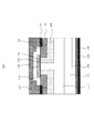
- the body layer 105 is formed as shown in FIG. 1 in order to form the body layer after recessing a part of the source diffusion layer region after the source diffusion layer region is formed. It is formed.
- the presence of the body layer 105 can widen the distance between each end with the source diffusion layer 102, effectively widen the depletion layer, and suppress electric field concentration at this end. It becomes possible.
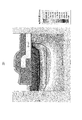
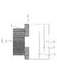
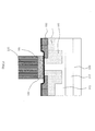
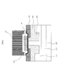
- FIG. 4 and FIG. 5 show the results of calculating the electric field distribution of the conventional structure and the structure of the present invention using a device simulator, respectively. It can be seen that the electric field concentration at the end of the body is suppressed in the structure of the present invention shown in FIG. 5 compared to the conventional structure in FIG.
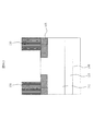
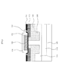
- FIG. 1 is an explanatory diagram showing a cross-sectional structure diagram of a silicon carbide semiconductor device in Example 1.
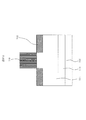
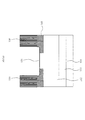
- FIG. FIG. 2 is an explanatory diagram showing a planar structure of the silicon carbide semiconductor device in the first embodiment. It is explanatory drawing which shows the cross-section figure of the silicon carbide semiconductor device in a prior art. It is sectional drawing. It is an electric field distribution map of the silicon carbide semiconductor device in the prior art calculated
- FIG. 1 is a schematic cross-sectional view of a silicon carbide semiconductor device of Example 1.
- the silicon carbide semiconductor device has a structure in which a plurality of DMOSFET unit cells are arranged. In FIG. 1, some of the plurality of unit cells are shown.
- Reference numeral 113 denotes an SiC substrate.
- the SiC substrate 113 and the epitaxial layer 112 formed on the SiC substrate 113 constitute an SiC epitaxial substrate.
- Body layers 105 and 106 constituting the channel region of the MOSFET and a source diffusion layer region 102 constituting the source region of the MOSFET are formed on the surface of the SiC epitaxial substrate.
- the channel region is 160.
- a drain diffusion layer region 108 that constitutes the drain region of the MOSFET is formed on the back surface of the SiC epitaxial substrate.
- Reference numeral 103 denotes a p + layer for fixing the potential of the body layers 105 and 106.
- Reference numeral 100 denotes a MOSFET gate electrode, and reference numeral 101 denotes a gate insulating film.
- Reference numeral 110 denotes an interlayer film.
- 107 is a metal silicide layer on the surface of the SiC epitaxial substrate, and 109 is a metal silicide layer on the back surface of the SiC epitaxial substrate.
- 111 is a wiring electrode to the source, and 140 is a wiring electrode to the drain on the back surface.
- 100 is a gate potential supplied from the outside via a wiring electrode to the gate, 111 is electrically connected to an external wiring to which a source potential is applied, and 140 also has a drain potential supplied from the outside. Applied.
- FIG. 2 is an explanatory diagram illustrating a planar structure of the semiconductor device according to the first embodiment.
- a semiconductor chip on which a silicon carbide semiconductor device is mounted includes an active region (SiC power MISFET forming region) 121 in which a plurality of n-channel SiC power MOSFETs are connected in parallel, and the active region in plan view.
- the peripheral forming region includes a plurality of p-type floating field limiting rings (FLR) 125 formed so as to surround the active region 121 in a plan view, and the plurality of the floating-type limiting ring (FLR) 125 in a plan view.
- An n + type guard ring 124 formed so as to surround the p type floating field limiting ring 125 is formed.
- the gate electrode of the SiC power MOSFET, n + -type source region of the channel region or the like is formed on the back surface side of the SiC epitaxial substrate, the SiC power MOSFET n + -type The drain region is formed.
- the maximum electric field portion is sequentially turned to the outer p-type floating field limiting ring 125 when off. Since the breakdown is caused by the outermost p-type floating field limiting ring, the silicon carbide semiconductor device can have a high breakdown voltage.
- FIG. 2 shows an example in which three p-type floating field limiting rings 125 are formed, the present invention is not limited to this.
- the n + -type guard ring 124 has a function of protecting the SiC power MOSFET formed in the active region 121.
- the gate electrodes of the plurality of SiC power MOSFETs formed in the active region 121 are connected to each other in a stripe pattern in a plan view, and all the lead wires (gate bus lines) connected to the respective stripe patterns are used.
- the gate electrode of the SiC power MOSFET is electrically connected to the gate wiring electrode 122.
- the gate electrode is formed in a stripe pattern, but the present invention is not limited to this, and examples include a box pattern and a polygon pattern.
- Each source region of the plurality of SiC power MOSFETs is electrically connected to the source wiring electrode 120 through an opening 123 formed in an interlayer insulating film covering the plurality of SiC power MOSFETs.
- the gate wiring electrode 122 and the source wiring electrode 120 are formed to be separated from each other, and the source wiring electrode 120 is formed on almost the entire surface of the active region 121 except for the region where the gate wiring electrode 122 is formed. Is formed.
- the n + type drain region formed on the back side of the n-type SiC epitaxial substrate is electrically connected to the drain wiring electrode formed on the entire back surface of the n-type SiC epitaxial substrate.
- a method for manufacturing the silicon carbide semiconductor device of Example 1 shown in FIG. 1 will be described.
- a body layer 105 is formed in order to form a body layer after recessing this part, and each end portion of the source diffusion layer 110 is compared with the conventional structure. This makes it possible to broaden the distance of the gate, effectively widen the depletion layer, suppress the electric field concentration at this edge, and reduce the gate length to reduce the channel resistance and achieve high device breakdown voltage.
- a silicon semiconductor device can be realized.
- the silicon carbide semiconductor device is provided on a 4H—SiC substrate.
- An n-type impurity is implanted into the SiC substrate.
- This impurity is, for example, nitrogen.
- the impurity concentration is in the range of 1 ⁇ 10 18 to 1 ⁇ 10 21 cm ⁇ 3 .
- the surface of the SiC substrate may be either a Si surface or a C (carbon) surface.
- An SiC n ⁇ -type epitaxial layer 112 in which an n-type impurity is implanted at a lower concentration than the SiC substrate 113 is epitaxially grown on the SiC substrate 113.
- the impurity concentration of n ⁇ -type epitaxial layer 112 depends on the element rating of the silicon carbide semiconductor device, but is, for example, in the range of 1 ⁇ 10 14 to 1 ⁇ 10 17 cm ⁇ 3 .
- the SiC epitaxial substrate is completed through the above steps.
- an n + type diffusion layer region 108 serving as a drain is provided on the back surface of the SiC epitaxial substrate.
- the impurity concentration is desirably high, for example, in the range of 1 ⁇ 10 19 to 1 ⁇ 10 21 cm ⁇ 3 (FIG. 6A).
- the source diffusion layer 102 is formed.
- the depth of the sole diffusion layer 102 is ⁇ 0.5 ⁇ , and the implantation energy is usually several hundred keV. Therefore, a hard mask such as SiO 2 (silicon oxide) is generally used as the mask.
- a SiO 2 film is deposited by about 1 to 3 ⁇ m using a plasma CVD (chemical vapor deposition) apparatus.
- a positive resist is applied, exposed, and developed to form a resist pattern having a desired body layer shape.
- the patterned mask 130 is formed on the SiC epitaxial substrate by processing the SiO 2 film by dry etching and removing the resist (FIG. 6B).
- an n + -type source diffusion layer region 102 is formed by ion implantation.
- the impurity is, for example, N (nitrogen).
- the impurity concentration is, for example, in the range of 1 ⁇ 10 19 to 1 ⁇ 10 21 cm ⁇ 3 (FIG. 6B).
- the p + layer 103 is formed in the silicide layer forming portion.
- a SiO 2 film is deposited by a plasma CVD apparatus.
- a positive resist is applied, exposed, and developed to form a resist pattern having a desired body layer shape.
- the patterned mask 130 is formed on the SiC epitaxial substrate by processing the SiO 2 film by dry etching and removing the resist (FIG. 6C).
- the p + layer 103 is formed by ion implantation.
- the impurity is, for example, Al.
- the impurity concentration is, for example, in the range of 1 ⁇ 10 19 to 1 ⁇ 10 21 cm ⁇ 3 (FIG. 6 (c)).
- a part of the source diffusion layer 102 is recessed to form the body layer 105.
- a SiO 2 film is deposited by a plasma CVD apparatus.
- a positive resist is applied, exposed, and developed to form a resist pattern having a desired body layer shape.
- the patterned mask 130 is formed on the SiC epitaxial substrate by processing the SiO 2 film by dry etching and removing the resist (FIG. 6D).
- a recess region 131 is formed on the source diffusion layer region 102 and the SiC epitaxial substrate by using, for example, dry etching (FIG. 6E).
- the depth of the recess is, for example, in the range of 10 to 200 nm.
- body layers 105 and 106 are formed.
- the depth of the body layer is as deep as 0.5 to 2 ⁇ m, and the implantation energy is usually several hundred keV to several MeV. Therefore, a hard mask such as SiO 2 (silicon oxide) is generally used as the mask.
- a SiO 2 film is deposited by about 1 to 3 ⁇ m using a plasma CVD (chemical vapor deposition) apparatus.
- a positive resist is applied, exposed, and developed to form a resist pattern having a desired body layer shape.
- the patterned mask 130 is formed on the SiC epitaxial substrate by processing the SiO 2 film by dry etching and removing the resist (FIG. 6F).
- a p-type impurity is implanted using ion implantation to form a body layer.
- the impurity is, for example, Al (aluminum).
- the impurity concentration is, for example, in the range of 1 ⁇ 10 16 to 1 ⁇ 10 19 cm ⁇ 3 (FIG. 6 (f)).
- the implanted impurities are activated.
- a temperature of 1500 ° C. or higher is required for the activation heat treatment of SiC.
- Si atoms and implanted impurities are detached from the surface of the SiC substrate.
- surface flatness will deteriorate. Therefore, the front and back surfaces of the SiC epitaxial substrate are covered with a carbon film before the activation heat treatment.
- the carbon film is deposited about 30 nm on the front and back surfaces of the SiC epitaxial substrate by a plasma CVD apparatus. After coating this carbon film, activation heat treatment is performed at a high temperature of 1500 ° C. or higher for several minutes. After the activation heat treatment, the coated carbon film is removed by oxygen plasma treatment.
- the SiC epitaxial substrate surface is edged in a high-temperature hydrogen atmosphere.
- the temperature at this time is preferably 1000 ° C. or higher. Also.
- the edge portion of the source diffusion layer region 102 formed by recessing can be rounded. It is desirable that the end of the channel region 207 on the side of the source diffusion layer region forms an angle with a curvature of 5 nm or more. Note that an element may be formed without performing this hydrogen heat treatment.
- the gate insulating film 101 and the gate electrode 100 are formed.
- the gate insulating film 101 it is preferable to use a SiON film as a SiC epitaxial substrate surface layer of the gate insulating film 101 using nitrogen monoxide gas.
- a SiO 2 film it is desirable to deposit a SiO 2 film by a thermal CVD apparatus so that the gate insulating film 101 is a multilayer film (FIG. 6G).
- the thickness of the gate insulating film 101 is in the range of 50 to 150 nm.
- a polycrystalline Si film 161 implanted with P is generally deposited (FIG. 6G).
- the thickness of the polycrystalline Si film 161 is in the range of 100 to 500 nm.
- the polycrystalline Si film 161 is processed.
- a positive resist is applied, exposed, and developed to form a resist pattern 132 having a desired gate electrode 100 shape.
- the Si film 161 is processed into a desired shape by dry etching to form the gate electrode 110 (FIG. 6H).
- the interlayer film 110 is deposited by a plasma CVD apparatus. Thereafter, the interlayer film 110 is baked at 1000 ° C., and then, in order to provide wiring electrodes on the source diffusion layer region 102 and the p + layer 103p + layer for fixing the potentials of the body layers 105 and 106
- the interlayer film 110 and part of the gate insulating film 101 are opened to form a contact region.
- a positive resist is applied, exposed, and developed to form a resist mask 132 for obtaining a desired opening shape.
- the interlayer film 110 and the gate insulating film 101 are processed into a desired shape by dry etching to form a contact region (FIG. 6I).
- a metal silicide layer 107 is formed on the source diffusion layer region 102 and the p + layer 103 in order to reduce the contact resistance between the source diffusion layer region 102, the p + layer 103, and the wiring electrode.
- a metal film is deposited by about 20 nm using a magnetron sputtering apparatus. After the metal film is deposited, silicidation annealing at 500 ° C. to 900 ° C. is performed to react the metal film with the SiC epitaxial substrate, thereby forming the metal silicide layer 107. Subsequently, the unreacted metal film is removed by wet etching. For this wet etching for removing the metal film, for example, sulfuric acid is used. (Fig. 6 (j))
- a metal silicide layer 109 is formed so as to cover the n + -type diffusion layer region 108 on the back surface.
- a metal film is deposited to a thickness of about 100 nm on the back surface of the SiC epitaxial substrate using a magnetron sputtering apparatus.
- a silicide at 800 ° C. to 1200 ° C. is annealed to react the metal film with the SiC epitaxial substrate to provide a metal silicide 109 (FIG. 6 (k)).
- a metal film 140 is deposited to a desired thickness so as to cover the metal silicide 109 on the back surface.
- a part of the interlayer film 110 is opened.
- a positive resist is applied, exposed, and developed to form a resist pattern having a desired gate opening shape.
- a wiring electrode 111 to the source and a wiring electrode to the gate are provided.
- the electrode titanium, titanium nitride, and aluminum are laminated by a metal CVD apparatus (FIG. 2- (r)).
- the film thickness of the aluminum film is preferably 2 ⁇ m or more in consideration of connection to the wiring.
- the wiring electrode 111 to the source and the wiring electrode to the gate are also separated. Thereafter, the wiring is connected to the wiring electrode to the source, and the wiring is also connected to the wiring electrode to the gate.
- the silicon carbide semiconductor device having the deep body layer 105 was formed.
- the body layer 105 is formed deeper than the conventional body layer 106 by forming the source diffusion layer region and then forming a body layer after recessing the source diffusion layer region. can do. Due to the presence of the body layer 105, the distance between the end portions of the source diffusion layer 102 can be increased compared to the conventional structure, the depletion layer is effectively expanded, the electric field concentration at this end portion is suppressed, The characteristics can be improved.
- DESCRIPTION OF SYMBOLS 100 ... Gate electrode, 101 ... Gate insulating film, 102 ... Source diffused layer, 103 ... P + layer, 105 ... Deep body layer, 106 ... Body layer, 107 ... Surface metal silicide layer, 108 ... drain diffusion layer region, 109 ... back metal silicide layer, 110 ... interlayer film, 111 ... source electrode, 112 ... SiC epitaxial layer, 113 ... SiC Substrate, 120 ... electrode for source wiring, 121 ... active region, 122 ... electrode for gate wiring, 123 ... opening, 124 ... guard ring, 125 ... p-type floating Field limiting ring, 130, 132 ... Mask layer, 131 ... Recess region, 140 ... Metal film, 160 ... Channel region
Landscapes
- Electrodes Of Semiconductors (AREA)
- Insulated Gate Type Field-Effect Transistor (AREA)
Abstract
Description
Claims (8)
- 第1主面および前記第1主面と反対面の第2主面を有し、炭化珪素からなる第1導電型の基板と、
前記基板の前記第1主面上に形成された炭化珪素からなるエピタキシャル層と、
前記エピタキシャル層内に形成された前記第1導電型とは異なる第2導電型の第1のボディ層と、
前記エピタキシャル層内に形成された前記第1導電型とは異なる第2導電型の第2のボディ層と、
前記第1のボディ層内に形成された前記第1導電型の第1のソース領域と、
前記第2のボディ層内に形成された前記第1導電型の第2のソース領域と、
前記第1のボディ層の横端部と前記第1のソース領域の横端部との間の前記第1のボディ層に位置する前記第1のソース領域に接して形成された前記第2導電型の第1チャネル領域と、
前記第2のボディ層の横端部と前記第2のソース領域の横端部との間の前記第2のボディ層に位置する前記第2のソース領域に接して形成された前記第2導電型の第2チャネル領域と、
前記第1チャネル領域と前記第2チャネル領域に接して形成されたゲート絶縁膜と、
前記ゲート絶縁膜に接して形成されたゲート電極と、
前記基板の前記第2主面から所定の深さを有して、前記基板に形成された前記第1導電型のドレイン領域と、
前記第1及び第2のソース領域と、前記第1及び第2のチャネル領域がリセスされていることを特徴とする炭化珪素半導体装置。 - 請求項1において、
前記ソース領域と、前記チャネル領域がリセスされた領域のボディ層の接合深さは、前記ソース領域のリセスされていない領域の接合深さよりも深くなっていることを特徴とする炭化珪素半導体装置。 - 請求項1において、
前記チャネル領域がリセスされた領域のボディ層の接合深さと、前記ソース領域のリセスされていない領域の接合深さ異なる横端部が、前記ソース領域のリセスされた横端部よりも、外側配置されていることを特徴とする炭化珪素半導体装置。 - 請求項1において、
前記ソース領域と、前記チャネル領域がリセスされた領域のボディ層の接合深さと、前記ソース領域のリセスされていない領域の接合深さの差が、10~200nmであることを特徴とする炭化珪素半導体装置。 - 第1主面および前記第1主面と反対面の第2主面を有し、炭化珪素からなる第1導電型の基板と、
前記基板の前記第1主面上に炭化珪素からなるエピタキシャル層を形成する工程と、
前記エピタキシャル層内に前記第1導電型とは異なる第2導電型の第1のボディ層を形成する工程と、
前記エピタキシャル層内に前記第1導電型とは異なる第2導電型の第2のボディ層を形成する工程と、
前記第1のボディ層内に前記第1導電型の第1のソース領域を形成する工程と、
前記第2のボディ層内に前記第1導電型の第2のソース領域を形成する工程と、
前記第1のボディ層の横端部と前記第1のソース領域の横端部との間の前記第1のボディ層に位置する前記第1のソース領域に接して前記第2導電型の第1チャネル領域を形成する工程と、
前記第2のボディ層の横端部と前記第2のソース領域の横端部との間の前記第2のボディ層に位置する前記第2のソース領域に接して前記第2導電型の第2チャネル領域を形成する工程と、
前記第1チャネル領域と前記第2チャネル領域に接してゲート絶縁膜を形成する工程と、
前記ゲート絶縁膜に接してゲート電極を形成する工程と、
前記基板の前記第2主面から所定の深さを有して、前記基板に前記第1導電型のドレイン領域を形成する工程と、
前記第1及び第2のソース領域と、前記第1及び第2のチャネル領域をリセスする工程と、
前記リセスした領域を形成した後に、ボディ層が形成されていることを特徴とする炭化珪素半導体装置の製造方法。 - 請求項5において、
前記ソース領域と、前記チャネル領域がリセスされた領域のボディ層の接合深さは、前記ソース領域のリセスされていない領域の接合深さよりも深く形成されていることを特徴とする炭化珪素半導体装置の製造方法。 - 請求項5において、
前記チャネル領域がリセスされた領域のボディ層の接合深さと、前記ソース領域のリセスされていない領域の接合深さ異なる横端部が、前記ソース領域のリセスされた横端部よりも、外側配置して形成されていることを特徴とする炭化珪素半導体装置の製造方法。 - 請求項5において、
前記ソース領域と、前記チャネル領域がリセスされた領域のボディ層の接合深さと、前記ソース領域のリセスされていない領域の接合深さの差が、10~200nmで形成されていることを特徴とする炭化珪素半導体装置の製造方法。
Priority Applications (4)
| Application Number | Priority Date | Filing Date | Title |
|---|---|---|---|
| US14/651,555 US9263571B2 (en) | 2012-12-28 | 2012-12-28 | Silicon carbide semiconductor device and manufacturing method thereof |
| JP2014553991A JP5996671B2 (ja) | 2012-12-28 | 2012-12-28 | 炭化珪素半導体装置及びその製造方法 |
| PCT/JP2012/084023 WO2014103000A1 (ja) | 2012-12-28 | 2012-12-28 | 炭化珪素半導体装置及びその製造方法 |
| DE112012007275.8T DE112012007275T5 (de) | 2012-12-28 | 2012-12-28 | Siliziumcarbid-Halbleitervorrichtung und Herstellungsverfahren dafür |
Applications Claiming Priority (1)
| Application Number | Priority Date | Filing Date | Title |
|---|---|---|---|
| PCT/JP2012/084023 WO2014103000A1 (ja) | 2012-12-28 | 2012-12-28 | 炭化珪素半導体装置及びその製造方法 |
Publications (1)
| Publication Number | Publication Date |
|---|---|
| WO2014103000A1 true WO2014103000A1 (ja) | 2014-07-03 |
Family
ID=51020151
Family Applications (1)
| Application Number | Title | Priority Date | Filing Date |
|---|---|---|---|
| PCT/JP2012/084023 Ceased WO2014103000A1 (ja) | 2012-12-28 | 2012-12-28 | 炭化珪素半導体装置及びその製造方法 |
Country Status (4)
| Country | Link |
|---|---|
| US (1) | US9263571B2 (ja) |
| JP (1) | JP5996671B2 (ja) |
| DE (1) | DE112012007275T5 (ja) |
| WO (1) | WO2014103000A1 (ja) |
Cited By (10)
| Publication number | Priority date | Publication date | Assignee | Title |
|---|---|---|---|---|
| WO2016076055A1 (ja) * | 2014-11-12 | 2016-05-19 | 富士電機株式会社 | 炭化珪素半導体スイッチング素子およびその製造方法 |
| JPWO2016110990A1 (ja) * | 2015-01-09 | 2017-06-22 | 株式会社日立製作所 | パワー半導体素子、パワーモジュール、および電力変換装置 |
| CN107919384A (zh) * | 2016-10-07 | 2018-04-17 | 丰田自动车株式会社 | 半导体器件 |
| JP2018101789A (ja) * | 2018-01-25 | 2018-06-28 | 株式会社日立製作所 | 半導体スイッチング素子および炭化珪素半導体装置の製造方法 |
| WO2022118509A1 (ja) * | 2020-12-02 | 2022-06-09 | 株式会社日立製作所 | 半導体装置 |
| JP2022144216A (ja) * | 2021-03-18 | 2022-10-03 | 株式会社東芝 | 半導体装置、半導体装置の製造方法、インバータ回路、駆動装置、車両、及び、昇降機 |
| JP2022144217A (ja) * | 2021-03-18 | 2022-10-03 | 株式会社東芝 | 半導体装置、半導体装置の製造方法、インバータ回路、駆動装置、車両、及び、昇降機 |
| JP2023530711A (ja) * | 2020-06-19 | 2023-07-19 | ウルフスピード インコーポレイテッド | ハイブリッド・ゲート構造を有するパワー・デバイス |
| KR20230171599A (ko) * | 2022-06-14 | 2023-12-21 | 재단법인 부산테크노파크 | 실리콘카바이드 모스펫 전력반도체의 셀프 얼라인 컨텍을 이용한 접합구조 형성방법 |
| US12199045B2 (en) | 2020-03-27 | 2025-01-14 | Wolfspeed, Inc. | Power semiconductor package with improved performance |
Families Citing this family (5)
| Publication number | Priority date | Publication date | Assignee | Title |
|---|---|---|---|---|
| JP2019075411A (ja) | 2017-10-12 | 2019-05-16 | 株式会社日立製作所 | 炭化ケイ素半導体装置、パワーモジュールおよび電力変換装置 |
| US10422818B2 (en) * | 2017-12-30 | 2019-09-24 | Texas Instruments Incorporated | Power transistors with a resistor coupled to a sense transistor |
| US11004940B1 (en) * | 2020-07-31 | 2021-05-11 | Genesic Semiconductor Inc. | Manufacture of power devices having increased cross over current |
| DE102021122629A1 (de) * | 2020-09-03 | 2022-03-17 | Hyundai Mobis Co., Ltd. | Leistungshalbleitervorrichtung und verfahren zur herstellung davon |
| WO2026065099A1 (zh) * | 2024-09-27 | 2026-04-02 | 湖南三安半导体有限责任公司 | 功率半导体器件 |
Citations (3)
| Publication number | Priority date | Publication date | Assignee | Title |
|---|---|---|---|---|
| JP2001094098A (ja) * | 1999-09-21 | 2001-04-06 | Denso Corp | 炭化珪素半導体装置及びその製造方法 |
| JP2002093742A (ja) * | 2000-09-18 | 2002-03-29 | National Institute Of Advanced Industrial & Technology | オーミック電極構造体、その製造方法、半導体装置及び半導体装置の製造方法 |
| JP2004335917A (ja) * | 2003-05-12 | 2004-11-25 | Nissan Motor Co Ltd | 半導体装置及びその製造方法 |
Family Cites Families (6)
| Publication number | Priority date | Publication date | Assignee | Title |
|---|---|---|---|---|
| JP2000357795A (ja) * | 1999-06-17 | 2000-12-26 | Nec Kansai Ltd | ディプレッション型半導体装置の製造方法 |
| JP2002208699A (ja) * | 2001-01-10 | 2002-07-26 | Toshiba Corp | 絶縁ゲート型半導体装置 |
| US6956239B2 (en) * | 2002-11-26 | 2005-10-18 | Cree, Inc. | Transistors having buried p-type layers beneath the source region |
| US7402844B2 (en) * | 2005-11-29 | 2008-07-22 | Cree, Inc. | Metal semiconductor field effect transistors (MESFETS) having channels of varying thicknesses and related methods |
| US8053344B1 (en) * | 2010-09-21 | 2011-11-08 | Taiwan Semiconductor Manufacturing Company, Ltd. | Methods of forming integrated circuits |
| WO2013140621A1 (ja) * | 2012-03-23 | 2013-09-26 | ルネサスエレクトロニクス株式会社 | 半導体装置およびその製造方法 |
-
2012
- 2012-12-28 DE DE112012007275.8T patent/DE112012007275T5/de not_active Withdrawn
- 2012-12-28 US US14/651,555 patent/US9263571B2/en not_active Expired - Fee Related
- 2012-12-28 WO PCT/JP2012/084023 patent/WO2014103000A1/ja not_active Ceased
- 2012-12-28 JP JP2014553991A patent/JP5996671B2/ja not_active Expired - Fee Related
Patent Citations (3)
| Publication number | Priority date | Publication date | Assignee | Title |
|---|---|---|---|---|
| JP2001094098A (ja) * | 1999-09-21 | 2001-04-06 | Denso Corp | 炭化珪素半導体装置及びその製造方法 |
| JP2002093742A (ja) * | 2000-09-18 | 2002-03-29 | National Institute Of Advanced Industrial & Technology | オーミック電極構造体、その製造方法、半導体装置及び半導体装置の製造方法 |
| JP2004335917A (ja) * | 2003-05-12 | 2004-11-25 | Nissan Motor Co Ltd | 半導体装置及びその製造方法 |
Cited By (17)
| Publication number | Priority date | Publication date | Assignee | Title |
|---|---|---|---|---|
| JPWO2016076055A1 (ja) * | 2014-11-12 | 2017-07-20 | 富士電機株式会社 | 炭化珪素半導体スイッチング素子およびその製造方法 |
| US9947750B2 (en) | 2014-11-12 | 2018-04-17 | Fuji Electric Co., Ltd. | Silicon carbide semiconductor switching device and method of manufacturing silicon carbide semiconductor switching device |
| WO2016076055A1 (ja) * | 2014-11-12 | 2016-05-19 | 富士電機株式会社 | 炭化珪素半導体スイッチング素子およびその製造方法 |
| JPWO2016110990A1 (ja) * | 2015-01-09 | 2017-06-22 | 株式会社日立製作所 | パワー半導体素子、パワーモジュール、および電力変換装置 |
| CN107919384A (zh) * | 2016-10-07 | 2018-04-17 | 丰田自动车株式会社 | 半导体器件 |
| CN107919384B (zh) * | 2016-10-07 | 2020-11-06 | 株式会社电装 | 半导体器件 |
| JP2018101789A (ja) * | 2018-01-25 | 2018-06-28 | 株式会社日立製作所 | 半導体スイッチング素子および炭化珪素半導体装置の製造方法 |
| US12199045B2 (en) | 2020-03-27 | 2025-01-14 | Wolfspeed, Inc. | Power semiconductor package with improved performance |
| JP7611944B2 (ja) | 2020-06-19 | 2025-01-10 | ウルフスピード インコーポレイテッド | ハイブリッド・ゲート構造を有するパワー・デバイス |
| JP2023530711A (ja) * | 2020-06-19 | 2023-07-19 | ウルフスピード インコーポレイテッド | ハイブリッド・ゲート構造を有するパワー・デバイス |
| WO2022118509A1 (ja) * | 2020-12-02 | 2022-06-09 | 株式会社日立製作所 | 半導体装置 |
| JP2022144216A (ja) * | 2021-03-18 | 2022-10-03 | 株式会社東芝 | 半導体装置、半導体装置の製造方法、インバータ回路、駆動装置、車両、及び、昇降機 |
| JP7476130B2 (ja) | 2021-03-18 | 2024-04-30 | 株式会社東芝 | 半導体装置、半導体装置の製造方法、インバータ回路、駆動装置、車両、及び、昇降機 |
| JP7547262B2 (ja) | 2021-03-18 | 2024-09-09 | 株式会社東芝 | 半導体装置、半導体装置の製造方法、インバータ回路、駆動装置、車両、及び、昇降機 |
| JP2022144217A (ja) * | 2021-03-18 | 2022-10-03 | 株式会社東芝 | 半導体装置、半導体装置の製造方法、インバータ回路、駆動装置、車両、及び、昇降機 |
| KR102699369B1 (ko) * | 2022-06-14 | 2024-08-26 | 재단법인부산테크노파크 | 실리콘카바이드 모스펫 전력반도체의 셀프 얼라인 컨텍을 이용한 접합구조 형성방법 |
| KR20230171599A (ko) * | 2022-06-14 | 2023-12-21 | 재단법인 부산테크노파크 | 실리콘카바이드 모스펫 전력반도체의 셀프 얼라인 컨텍을 이용한 접합구조 형성방법 |
Also Published As
| Publication number | Publication date |
|---|---|
| US20150318389A1 (en) | 2015-11-05 |
| JPWO2014103000A1 (ja) | 2017-01-12 |
| JP5996671B2 (ja) | 2016-09-21 |
| DE112012007275T5 (de) | 2015-11-12 |
| US9263571B2 (en) | 2016-02-16 |
Similar Documents
| Publication | Publication Date | Title |
|---|---|---|
| JP5996671B2 (ja) | 炭化珪素半導体装置及びその製造方法 | |
| JP6168732B2 (ja) | 炭化珪素半導体装置およびその製造方法 | |
| JP6140823B2 (ja) | 炭化珪素半導体装置 | |
| US9825166B2 (en) | Silicon carbide semiconductor device and method for producing same | |
| JP6277623B2 (ja) | ワイドバンドギャップ半導体装置 | |
| US9117836B2 (en) | Silicon carbide semiconductor device and manufacturing method thereof | |
| JP5994604B2 (ja) | 炭化珪素半導体装置およびその製造方法 | |
| WO2015015934A1 (ja) | ワイドバンドギャップ半導体装置 | |
| US10381444B2 (en) | Manufacturing method of semiconductor device | |
| US8941120B2 (en) | Semiconductor device and method for manufacturing the same | |
| JP6991476B2 (ja) | 半導体装置 | |
| US9048251B2 (en) | Semiconductor device and method of manufacturing the same | |
| US8809945B2 (en) | Semiconductor device having angled trench walls | |
| WO2017051616A1 (ja) | 炭化珪素半導体装置およびその製造方法 | |
| WO2014192437A1 (ja) | 炭化珪素半導体装置 | |
| US9324860B2 (en) | Semiconductor device | |
| JP5875334B2 (ja) | 炭化珪素半導体装置 | |
| WO2014102994A1 (ja) | 炭化珪素半導体装置及びその製造方法 | |
| JP2009070849A (ja) | 半導体装置 | |
| JP4972293B2 (ja) | 半導体装置およびその製造方法 | |
| JP2022052774A (ja) | 炭化珪素半導体装置 | |
| KR101371491B1 (ko) | 반도체 소자 및 그 제조 방법 |
Legal Events
| Date | Code | Title | Description |
|---|---|---|---|
| 121 | Ep: the epo has been informed by wipo that ep was designated in this application |
Ref document number: 12891312 Country of ref document: EP Kind code of ref document: A1 |
|
| ENP | Entry into the national phase |
Ref document number: 2014553991 Country of ref document: JP Kind code of ref document: A |
|
| WWE | Wipo information: entry into national phase |
Ref document number: 14651555 Country of ref document: US |
|
| WWE | Wipo information: entry into national phase |
Ref document number: 1120120072758 Country of ref document: DE Ref document number: 112012007275 Country of ref document: DE |
|
| 122 | Ep: pct application non-entry in european phase |
Ref document number: 12891312 Country of ref document: EP Kind code of ref document: A1 |