WO2014097701A1 - 積層セラミック電子部品およびその製造方法 - Google Patents
積層セラミック電子部品およびその製造方法 Download PDFInfo
- Publication number
- WO2014097701A1 WO2014097701A1 PCT/JP2013/075783 JP2013075783W WO2014097701A1 WO 2014097701 A1 WO2014097701 A1 WO 2014097701A1 JP 2013075783 W JP2013075783 W JP 2013075783W WO 2014097701 A1 WO2014097701 A1 WO 2014097701A1
- Authority
- WO
- WIPO (PCT)
- Prior art keywords
- ceramic
- external electrode
- conductive paste
- multilayer ceramic
- glass
- Prior art date
- Legal status (The legal status is an assumption and is not a legal conclusion. Google has not performed a legal analysis and makes no representation as to the accuracy of the status listed.)
- Ceased
Links
Images


Classifications
-
- H—ELECTRICITY
- H01—ELECTRIC ELEMENTS
- H01G—CAPACITORS; CAPACITORS, RECTIFIERS, DETECTORS, SWITCHING DEVICES, LIGHT-SENSITIVE OR TEMPERATURE-SENSITIVE DEVICES OF THE ELECTROLYTIC TYPE
- H01G4/00—Fixed capacitors; Processes of their manufacture
- H01G4/30—Stacked capacitors
-
- H—ELECTRICITY
- H01—ELECTRIC ELEMENTS
- H01G—CAPACITORS; CAPACITORS, RECTIFIERS, DETECTORS, SWITCHING DEVICES, LIGHT-SENSITIVE OR TEMPERATURE-SENSITIVE DEVICES OF THE ELECTROLYTIC TYPE
- H01G4/00—Fixed capacitors; Processes of their manufacture
- H01G4/002—Details
- H01G4/005—Electrodes
- H01G4/012—Form of non-self-supporting electrodes
-
- H—ELECTRICITY
- H01—ELECTRIC ELEMENTS
- H01G—CAPACITORS; CAPACITORS, RECTIFIERS, DETECTORS, SWITCHING DEVICES, LIGHT-SENSITIVE OR TEMPERATURE-SENSITIVE DEVICES OF THE ELECTROLYTIC TYPE
- H01G4/00—Fixed capacitors; Processes of their manufacture
- H01G4/002—Details
- H01G4/018—Dielectrics
- H01G4/06—Solid dielectrics
- H01G4/08—Inorganic dielectrics
- H01G4/12—Ceramic dielectrics
- H01G4/1209—Ceramic dielectrics characterised by the ceramic dielectric material
- H01G4/1218—Ceramic dielectrics characterised by the ceramic dielectric material based on titanium oxides or titanates
- H01G4/1227—Ceramic dielectrics characterised by the ceramic dielectric material based on titanium oxides or titanates based on alkaline earth titanates
-
- H—ELECTRICITY
- H01—ELECTRIC ELEMENTS
- H01G—CAPACITORS; CAPACITORS, RECTIFIERS, DETECTORS, SWITCHING DEVICES, LIGHT-SENSITIVE OR TEMPERATURE-SENSITIVE DEVICES OF THE ELECTROLYTIC TYPE
- H01G4/00—Fixed capacitors; Processes of their manufacture
- H01G4/002—Details
- H01G4/228—Terminals
- H01G4/232—Terminals electrically connecting two or more layers of a stacked or rolled capacitor
-
- H—ELECTRICITY
- H01—ELECTRIC ELEMENTS
- H01G—CAPACITORS; CAPACITORS, RECTIFIERS, DETECTORS, SWITCHING DEVICES, LIGHT-SENSITIVE OR TEMPERATURE-SENSITIVE DEVICES OF THE ELECTROLYTIC TYPE
- H01G4/00—Fixed capacitors; Processes of their manufacture
- H01G4/002—Details
- H01G4/228—Terminals
- H01G4/232—Terminals electrically connecting two or more layers of a stacked or rolled capacitor
- H01G4/2325—Terminals electrically connecting two or more layers of a stacked or rolled capacitor characterised by the material of the terminals
-
- H—ELECTRICITY
- H01—ELECTRIC ELEMENTS
- H01G—CAPACITORS; CAPACITORS, RECTIFIERS, DETECTORS, SWITCHING DEVICES, LIGHT-SENSITIVE OR TEMPERATURE-SENSITIVE DEVICES OF THE ELECTROLYTIC TYPE
- H01G4/00—Fixed capacitors; Processes of their manufacture
- H01G4/002—Details
- H01G4/228—Terminals
- H01G4/248—Terminals the terminals embracing or surrounding the capacitive element, e.g. caps
-
- H—ELECTRICITY
- H01—ELECTRIC ELEMENTS
- H01G—CAPACITORS; CAPACITORS, RECTIFIERS, DETECTORS, SWITCHING DEVICES, LIGHT-SENSITIVE OR TEMPERATURE-SENSITIVE DEVICES OF THE ELECTROLYTIC TYPE
- H01G4/00—Fixed capacitors; Processes of their manufacture
- H01G4/002—Details
- H01G4/018—Dielectrics
- H01G4/06—Solid dielectrics
- H01G4/08—Inorganic dielectrics
- H01G4/12—Ceramic dielectrics
-
- Y—GENERAL TAGGING OF NEW TECHNOLOGICAL DEVELOPMENTS; GENERAL TAGGING OF CROSS-SECTIONAL TECHNOLOGIES SPANNING OVER SEVERAL SECTIONS OF THE IPC; TECHNICAL SUBJECTS COVERED BY FORMER USPC CROSS-REFERENCE ART COLLECTIONS [XRACs] AND DIGESTS
- Y10—TECHNICAL SUBJECTS COVERED BY FORMER USPC
- Y10T—TECHNICAL SUBJECTS COVERED BY FORMER US CLASSIFICATION
- Y10T29/00—Metal working
- Y10T29/43—Electric condenser making
- Y10T29/435—Solid dielectric type
Definitions
- the present invention relates to a multilayer ceramic electronic component and a method for manufacturing the same, and more particularly to a multilayer ceramic electronic component in which an external electrode is formed by heat treatment (baking) of a conductive paste containing a glass component and a method for manufacturing the same. .
- wet plating such as electrolytic plating is usually applied on an external electrode formed by baking to form, for example, a Ni plating film and a Sn plating film thereon.
- the mountability is improved, and more specifically, the solderability of the external electrode is improved.
- the plating solution used in carrying out wet plating as described above has a more or less undesirable effect on ceramic electronic components such as multilayer ceramic capacitors.
- the multilayer ceramic capacitor 1 includes a rectangular parallelepiped ceramic body 2.
- the ceramic body 2 is composed of a plurality of laminated ceramic layers, and internal electrodes (not shown) are arranged along a plurality of interfaces between the ceramic layers.
- External electrodes 3 and 4 are formed on a pair of opposing end faces of the ceramic body 2, respectively.
- the external electrodes 3 and 4 are electrically connected to the internal electrodes described above.
- the external electrodes 3 and 4 have respective edge portions 5 and 6 located on a pair of main surfaces 7 and 8 facing each other and a pair of side surfaces 9 and 10 facing each other of the ceramic body 2. .
- plating films 11 and 12 are formed on the external electrodes 3 and 4 by wet plating.
- FIG. 4 shows a state before the plating films 11 and 12 are formed.
- the plating solution deteriorates the ceramic body 2 particularly in the portion where the edge portions 5 and 6 of the external electrodes 3 and 4 are located. This will be described with reference to FIG.
- FIG. 6 is a cross-sectional view showing a part of the multilayer ceramic capacitor 1 in an enlarged manner, and schematically shows a portion where the edge 5 of one external electrode 3 is located in the ceramic body 2.
- illustration of the plating films 11 and 12 is omitted.
- a glass phase 15 is generated on the external electrode 3 by the glass component contained in the conductive paste.
- the glass phase 15 is distributed at a plurality of locations in the external electrode 3.
- the glass component in the conductive paste penetrates into the grain boundaries 17 between the ceramic particles 16 of the ceramic body 2 to form a reaction phase 18.
- the same phenomenon as that of the illustrated external electrode 3 occurs on the other external electrode 4 side.
- the external electrode 3 that is easy to touch the plating solution among the glass components that have penetrated the grain boundaries 17 between the ceramic particles 16.
- the glass component located in the vicinity of the edge portions 5 and 6 of 4 and 4 is melted by the plating solution, and as a result, the ceramic body 2 is eroded in the vicinity of the edge portions 5 and 6 of the external electrodes 3 and 4. End up. It can be presumed that the occurrence of the crack 14 described above is caused by weakening due to this erosion.
- Patent Document 1 Japanese Patent No. 4577461 (Patent Document 1) describes a conductive paste containing glass frit having a SiO 2 content of 7 wt% or more and 63 wt% or less.
- Patent Document 1 describes a conductive paste containing glass frit having a SiO 2 content of 7 wt% or more and 63 wt% or less.
- the above-described problem is caused by the plating solution used when forming the plating film on the external electrode.
- the same problem can be caused not only by the plating solution but also by other causes. Therefore, the same problem may be encountered even in a multilayer ceramic electronic component in which the external electrode is not plated.
- an object of the present invention is to provide a multilayer ceramic electronic component and a method for manufacturing the same, which can solve the above-described problems.
- the present invention relates to a ceramic body comprising a plurality of laminated ceramic layers, an internal electrode disposed along a plurality of interfaces between the ceramic layers, and a ceramic element so as to be electrically connected to the internal electrodes.
- an external body in a ceramic body is first directed to a multilayer ceramic electronic component comprising an external electrode formed on the outer surface of the body and containing a glass component.
- a crystalline material containing an element constituting a glass component contained in the external electrode is present at the grain boundary between the ceramic particles located at the portion in contact with the edge of the electrode.
- the above-mentioned crystalline material has, for example, resistance to dissolution or acid resistance to the plating solution, and suppresses the penetration of the plating solution or the like into the ceramic body.
- the present invention is advantageously applied particularly to a multilayer ceramic electronic component further including a plating film formed by wet plating on an external electrode.
- the crystalline material preferably contains Ba, Ti, and Si.
- the crystal is preferably present in a region having a thickness of 0.5 ⁇ m or more from the interface between the external electrode and the ceramic body toward the inside of the ceramic body.
- the weather resistance of the multilayer ceramic electronic component can be further improved.
- the present invention is also directed to a method for manufacturing a multilayer ceramic electronic component.
- a method for manufacturing a multilayer ceramic electronic component according to the present invention comprises a step of preparing a ceramic body, comprising a plurality of laminated ceramic layers, wherein internal electrodes are disposed along a plurality of interfaces between ceramic layers.
- the step of forming the external electrode includes the step of forming the ceramic body coated with the conductive paste with a top temperature of 800 ° C. or more. And a step of heat treatment under an atmospheric condition where the electromotive force at the top temperature is 600 to 900 mV, and in the heat treatment step, the glass component in the conductive paste penetrates into the grain boundaries between the ceramic particles of the ceramic body, It is characterized in that a crystal containing an element constituting a glass component is generated at a grain boundary between ceramic particles located in a portion in contact with an edge of the external electrode in the ceramic body.
- the present invention is advantageously applied particularly to a method for manufacturing a multilayer ceramic electronic component, further comprising a step of forming a plating film on the external electrode by wet plating.
- the multilayer ceramic electronic component According to the multilayer ceramic electronic component according to the present invention, at least the crystalline material having resistance to the plating solution exists in the grain boundary between the ceramic particles located in the portion in contact with the edge of the external electrode in the ceramic body. Therefore, for example, when the plating step is performed, the ceramic body is prevented from being eroded by the plating solution in the vicinity of the edge portion of the external electrode and becoming brittle. Therefore, it is possible to advantageously suppress the generation of cracks starting from the portion where the edge of the external electrode is positioned as described above with reference to FIG. As a result, the mechanical strength of the multilayer ceramic electronic component can be increased.
- the multilayer ceramic electronic component having the characteristic configuration as described above, that is, between the ceramic particles located in the portion in contact with the edge of the external electrode in the ceramic body.
- a multilayer ceramic electronic component in which a crystal substance containing an element constituting a glass component contained in the external electrode exists in the grain boundary can be reliably produced.
- FIG. 2 is a cross-sectional view showing a part of the multilayer ceramic capacitor 21 shown in FIG. 1 in an enlarged manner, and a portion where an edge portion 34 of one external electrode 32 is located in a ceramic body 22 while omitting illustration of a plating film. Is schematically shown. It is a figure for demonstrating the thickness of the reaction phase calculated
- FIG. 1 is a plan view illustrating a state in which a crack 13 is formed in a multilayer ceramic capacitor 1 before plating in order to explain a problem to be solved by the present invention.
- FIG. 1 is a plan view illustrating a state in which cracks 14 are formed in a multilayer ceramic capacitor 1 after plating in order to explain a problem to be solved by the present invention.
- FIG. 6 is a diagram corresponding to FIG. 2, showing an enlarged part of the multilayer ceramic capacitor 1 shown in FIGS. 4 and 5.
- a multilayer ceramic capacitor 21 includes a multilayer ceramic body 22 composed of a plurality of multilayered ceramic layers 23. Inside the ceramic body 22, a plurality of first and second internal electrodes 24 and 25 are arranged along a plurality of interfaces between the ceramic layers 23, respectively. The first internal electrode 24 and the second internal electrode 25 are opposed to each other in a part of each, and are alternately arranged as viewed in the stacking direction.
- the internal electrodes 24 and 25 are mainly composed of nickel, for example.
- the ceramic body 22 includes first and second main surfaces 26 and 27 facing each other, first and second side surfaces facing each other (a surface parallel to a paper surface not shown), and first and second surfaces facing each other. It has a substantially rectangular parallelepiped shape with end faces 30 and 31.
- Each end of the first internal electrode 24 is exposed on the first end face 30 of the ceramic body 22.
- a first external electrode 32 is formed on the first end face 30 of the ceramic body 22 so as to be electrically connected to each end of the first internal electrode 24.
- Each end of the second internal electrode 25 is exposed on the second end face 31 of the ceramic body 22.
- a second external electrode 33 is formed on the second end face 31 of the ceramic body 22 so as to be electrically connected to each end of the second internal electrode 25.
- the first and second external electrodes 32 and 33 have respective end edges 34 and 35 located on the main surfaces 26 and 27 adjacent to the end surfaces 30 and 31, and are not shown in this embodiment. Is also located on the side.
- the external electrodes 32 and 33 are formed by applying a conductive paste on the ceramic body 22 and subjecting it to heat treatment (baking). The details of this heat treatment will be described later.
- plating films 36 and 37 are formed as necessary.
- the plating films 36 and 37 are composed of a nickel plating layer 38 mainly containing nickel and a tin plating layer 39 mainly containing tin formed thereon.
- a ceramic body 22 is prepared.
- a ceramic green sheet containing a dielectric ceramic material is prepared, and then a conductive paste film to be the internal electrodes 24 and 25 with a predetermined pattern is formed on the ceramic green sheet,
- a plurality of ceramic green sheets including a ceramic green sheet on which a conductive paste film is formed is laminated to obtain a raw mother block, and then the mother block is cut to obtain individual mother ceramic capacitors 21.
- External electrodes 32 and 33 are formed on the ceramic body 22 obtained as described above.
- a conductive paste is prepared.
- the conductive paste includes conductive metal powder, glass frit and varnish.
- a copper powder having a D50 of 0.5 to 5.0 ⁇ m is used as the conductive metal powder.
- the glass frit is preferably a SiO 2 —B 2 O 3 —ZnO-based glass containing SiO 2 , B 2 O 3 and ZnO in a molar ratio of 10 to 50: 5 to 50: 0 to 40. Is used.
- the glass frit contains, in addition to SiO 2 , B 2 O 3 and ZnO, at least one selected from alkali metal oxides, alkaline earth metal oxides, Al 2 O 3 , TiO 2 and ZrO 2. You may go out.
- the softening point of the glass constituting the glass frit is set to 550 to 650 ° C., for example.
- the glass frit content is such that the solid content in the conductive paste (conductive metal powder + glass frit) is secured in order to ensure the denseness of the external electrodes 32 and 33 and the adhesion of the external electrodes 32 and 33 to the ceramic body 22.
- the content is preferably 18 to 22% by volume.
- the varnish for example, a solution obtained by dissolving an acrylic resin in an organic solvent mainly containing terpineol can be used.
- the conductive paste described above is applied onto the ceramic body 22 so as to be electrically connected to the internal electrodes 24 and 25, and then heat treated (baked) to form the external electrodes 32 and 33.
- the glass phase 40 is generated by the glass component contained in the conductive paste.
- the glass phase 40 is distributed at a plurality of locations in the external electrode 32.
- the glass component in the conductive paste penetrates into the grain boundaries 42 between the ceramic particles 41 of the ceramic body 22 to form a reaction phase 43.
- a phenomenon similar to that of the illustrated external electrode 32 side occurs on the other external electrode 33 side. The above phenomenon is the same as the phenomenon described above with reference to FIG.
- a feature of the present invention is that, in the above-described heat treatment step, a temperature condition where the top temperature is 800 ° C. or higher and an atmospheric condition where the electromotive force at the top temperature is 600 to 900 mV are applied.
- the glass component that has penetrated into the grain boundary 42 between the ceramic particles 41 of the ceramic body 22 generates a crystal containing the elements constituting the glass component. .
- the cause of the generation of the crystal containing the elements constituting the glass component that is, the cause of the glass crystallization will be considered.
- the following two points can be considered as the cause of the crystallization of the glass.
- a glass frit in a conductive paste for forming an external electrode is made of SiO 2 —B 2 O 3 —ZnO-based glass.
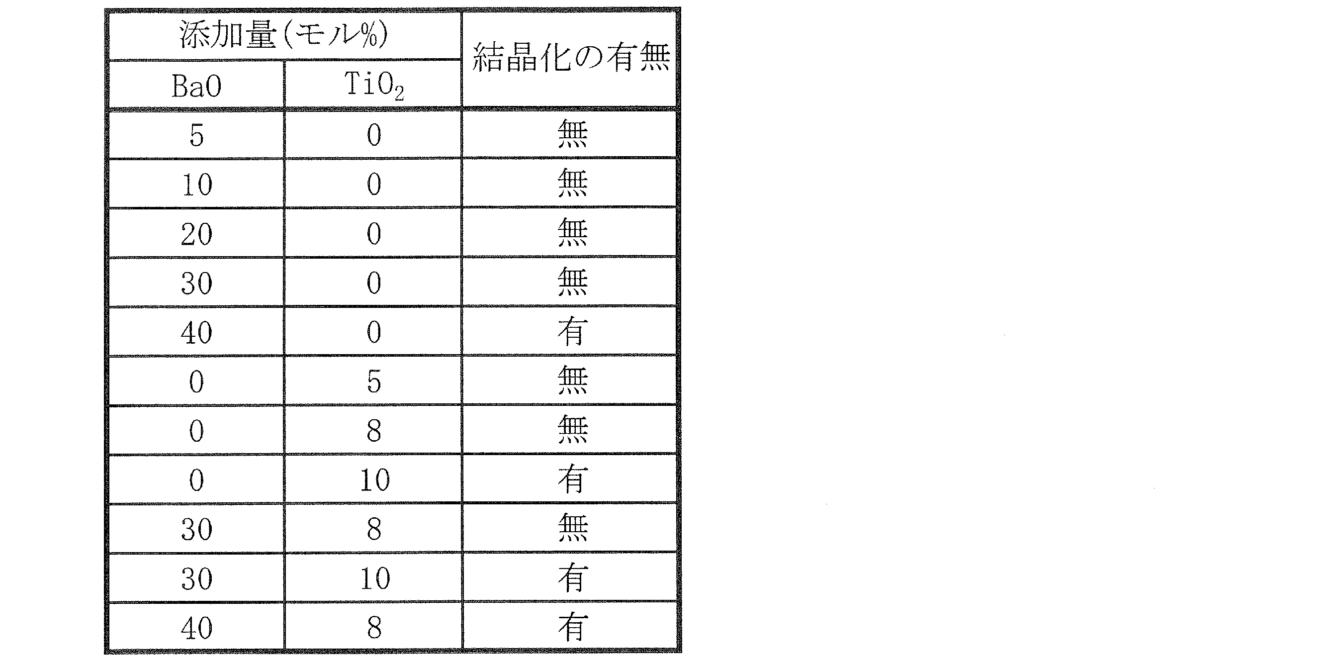
- the conductive paste is baked in a reducing atmosphere with an electromotive force of 600 to 900 mV, ZnO contained in the glass composition in the conductive paste is easily sublimated, and the glass composition after baking of the conductive paste changes. Thus, it becomes easier to crystallize. That is, the vitrification range is narrowed.
- the SiO 2 content in the glass composition calculated by removing ZnO from the glass composition in the conductive paste is 40 mol% or more.
- the glass composition in the conductive paste is desirably the amount of SiO 2 in the glass composition as calculated except ZnO of 40 mol% or more, after heat treatment for formation of external electrodes (baking) You may mix several types of glass so that it may become such a composition as a total.
- silica glass SiO 2
- a condition setting such as increasing the top temperature holding time to 60 to 120 hours can be considered.
- heat treatment for forming the external electrode may be performed a plurality of times.
- the plating films 36 and 37 are formed on the external electrodes 32 and 33 by performing wet plating such as electrolytic plating.
- wet plating such as electrolytic plating.
- the glass components located in the vicinity of the edge portions 34 and 35 of the external electrodes 32 and 33 are easy to touch the plating solution.
- the crystal generated in the grain boundary 42 has resistance to dissolution in, for example, Ni plating solution or Sn plating solution used in the plating step
- the ends of the external electrodes 32 and 33 are used in the plating step.
- the ceramic body 22 is prevented from being eroded and fragile. Therefore, it is possible to advantageously suppress the occurrence of cracks starting from the portions where the edge portions 34 and 35 of the external electrodes 32 and 33 are located, and as a result, the mechanical strength of the multilayer ceramic capacitor 21 can be increased. .
- the ceramic layer 23 is composed of a dielectric ceramic.
- the multilayer ceramic electronic component to which the present invention is applied may be an inductor, a thermistor, a piezoelectric component, or the like. Therefore, according to the function of the multilayer ceramic electronic component, the ceramic layer may be composed of a dielectric ceramic, a magnetic ceramic, a semiconductor ceramic, a piezoelectric ceramic, or the like.
- the illustrated multilayer ceramic capacitor 21 is a two-terminal type including two external electrodes 32 and 33, but the present invention can also be applied to a multi-terminal type multilayer ceramic electronic component.
- Example 1 Production of ceramic body A plurality of ceramic green sheets containing ceramic material powders mainly composed of Ba and Ti were prepared. Next, a conductive paste containing Ni as a main component was applied on the ceramic green sheet by screen printing to form a conductive paste film to be an internal electrode.
- the ceramic green sheets on which the conductive paste film is not formed are stacked so as to have a predetermined outer layer thickness, and then a predetermined number of ceramic green sheets on which the conductive paste film is formed are stacked.
- a green mother block in which a plurality of ceramic bodies can be taken out was obtained by laminating ceramic green sheets having no paste formed so as to have a predetermined outer layer thickness.
- the mother block was cut, a plurality of chip-shaped raw ceramic bodies were taken out, and then the raw ceramic bodies were fired in a reducing furnace in a reducing atmosphere to obtain a sintered ceramic body. .
- a conductive paste for external electrodes was obtained by dispersing and mixing a varnish obtained by dissolving an acrylic resin in an organic solvent.
- the glass frit contains SiO 2 , B 2 O 3 and ZnO in a molar ratio of 30:25:15 so that the amount of SiO 2 in the glass composition calculated excluding ZnO is 40 mol%. I made it.
- the glass amount relative to the solid content (Cu powder and glass frit) in the conductive paste was set to 20% by volume.
- a film made of the conductive paste for external electrodes is formed with a predetermined thickness on a surface plate, and the ceramic body held by the holder in the conductive paste film After the end portion of the ceramic body was dipped, the conductive paste to be external electrodes was applied to both end faces of the ceramic body by taking out the conductive paste film.
- the ceramic body on which the external electrode conductive paste film was formed was heat-treated in a belt furnace to form the baked external electrode on the ceramic body.
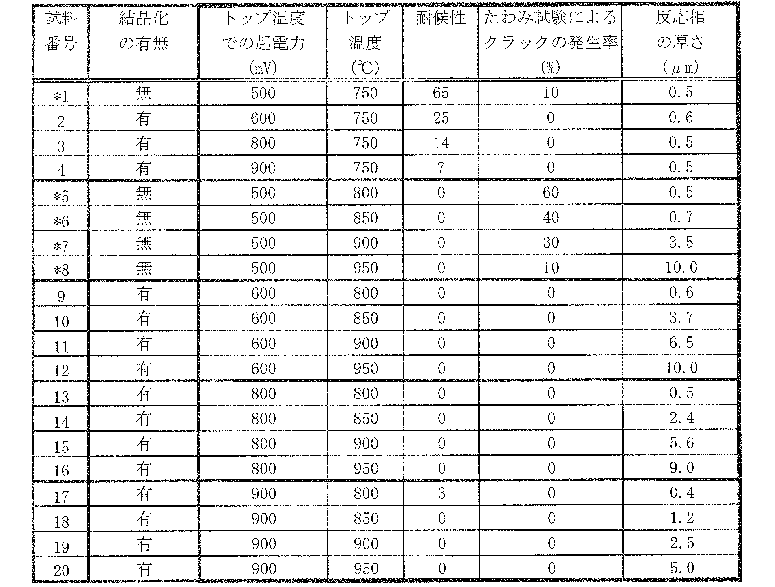
- a temperature condition for maintaining the top temperature shown in the column of “top temperature” in Table 2 for 5 minutes is adopted.
- H 2 is added to N 2 as a carrier gas at the top temperature.
- an atmosphere showing the reducing power to be an electromotive force shown in the column of “electromotive force at top temperature” in Table 2 was obtained.
- Ni electrolytic plating and Sn electrolytic plating were sequentially performed on the external electrode to form a plating film.
- Evaluation (5) -1 Observation of edge portion of external electrode Polished surface obtained by polishing multilayer ceramic capacitor according to each sample from surface defined by length direction dimension and thickness direction dimension to 1 ⁇ 2 of width direction dimension With respect to the ceramic body, one arbitrary place at the portion in contact with the edge of the external electrode in the ceramic body was observed at a magnification of 100,000 to 200,000 times using a TEM (transmission electron microscope).
- mapping analysis is performed on Si and Ba at a magnification of 100,000 to 200,000 at the location observed by TEM, and the grain boundary (Si) and the particles are closer to the ceramic body side than the interface between the external electrode and the ceramic body. Differentiated from (Ba).
- the number of samples evaluated as described above was 20 for each sample.
- the crystal was an oxide containing Ba, Ti, and Si.
- the multilayer ceramic capacitor after the above deflection test was removed from the substrate and polished from the surface defined by the length direction dimension and the thickness direction dimension to 1 ⁇ 2 of the width direction dimension. And the part which touches the external electrode edge part in a ceramic body in a grinding
- the column of “crack generation rate by deflection test” in Table 2 the ratio [%] of samples in which cracks occurred in 20 samples is shown.
- the insulation resistance of the multilayer ceramic capacitor after the moisture resistance load test is measured, and the one whose resistance value has decreased by one digit or more compared to the insulation resistance before the test is judged as a defective product.
- the silicon concentration distribution is obtained by performing line analysis along the thickness direction of the reaction phase, and after obtaining the analysis result as shown in FIG. 3, the silicon concentration gradient shown in FIG. By looking, the thickness of the reaction phase was determined.
- the column of “Reaction Phase Thickness” in Table 2 average values for five samples are shown.
- the polished surface of the sample polished from the surface defined by the length direction dimension and the thickness direction dimension to 1 ⁇ 2 of the width direction dimension is in contact with the edge of the external electrode in the ceramic body.
- the part was observed using a FE-SEM (Field Emission Scanning Electron Microscope) at a magnification of 10,000 times, and then the same sample was subjected to a Ni plating solution at 60 ° C. for 2 hours and a Sn plating solution at 25 ° C. for 1 hour. After each immersion, the portion of the ceramic body in contact with the edge of the external electrode on the polished surface was again observed using FE-SEM.
- the “top temperature” was 750 ° C., which is less than 800 ° C. In this way, when the “top temperature” is less than 800 ° C., even if the “electromotive force at the top temperature” is changed in the range of 500 to 900 mV, the denseness of the external electrode is low, so the “weather resistance” is reduced. did. In these samples 1 to 4, there was a tendency that as the “electromotive force at the top temperature” was higher, that is, the reducing power in the heat treatment atmosphere was stronger, the “weather resistance” was better.
- top temperature 800 ° C. or higher and “electromotive force at top temperature” is in the range of 600 to 900 mV
- a multilayer ceramic capacitor sample having “existence of crystallization” as “present” and “crack generation rate by deflection test” as 0% could be obtained with certainty.
- reaction phase thickness was 0.4 ⁇ m, and three defective products were produced in “weather resistance”.
Landscapes
- Engineering & Computer Science (AREA)
- Power Engineering (AREA)
- Manufacturing & Machinery (AREA)
- Microelectronics & Electronic Packaging (AREA)
- Chemical & Material Sciences (AREA)
- Ceramic Engineering (AREA)
- Inorganic Chemistry (AREA)
- Ceramic Capacitors (AREA)
- Fixed Capacitors And Capacitor Manufacturing Machines (AREA)
Abstract
Description
(1)セラミック素体の作製
BaおよびTiを主成分とするセラミック材料粉末を含む複数のセラミックグリーンシートを用意した。次に、セラミックグリーンシート上に、Niを主成分とする導電性ペーストをスクリーン印刷により塗布し、内部電極となるべき導電性ペースト膜を形成した。
Cu粉末(D50=1.5μm)と、軟化点:600℃のSiO2-B2O3-ZnO系ガラスからなるガラスフリットと、ターピネオールを主成分とする有機溶剤にアクリル系樹脂を溶解してなるワニスとを、分散・混合することによって、外部電極用の導電性ペーストを得た。
次に、定盤上に上記外部電極用導電性ペーストからなる膜を所定の厚みで形成しておき、この導電性ペースト膜中に、ホルダによって保持されたセラミック素体の端部を浸漬した後、導電性ペースト膜から取り出すことによって、セラミック素体の両端面に外部電極となる導電性ペーストを塗布した。
上記外部電極上に、Ni電解めっきおよびSn電解めっきを順次施し、めっき膜を形成した。
(5)-1.外部電極の端縁部の観察
各試料に係る積層セラミックコンデンサを、長さ方向寸法と厚み方向寸法とによって規定される面から幅方向寸法の1/2になるまで研磨して得られた研磨面について、セラミック素体における外部電極の端縁部に接する部分での任意の1箇所を、TEM(透過型電子顕微鏡)を用いて100000~200000倍の倍率で観察した。
ガラスエポキシ基板に、各試料に係る積層セラミックコンデンサをはんだで実装し、1.0mm/秒の速度で荷重を加え、たわみ量が1.5mmに達してから5±1秒間保持した。
各試料に係る積層セラミックコンデンサをガラスエポキシ基板に実装し、試験前の積層セラミックコンデンサの絶縁抵抗を測定した。
各試料に係る積層セラミックコンデンサを、長さ方向寸法と厚み方向寸法とによって規定される面から幅方向寸法の1/2になるまで研磨して得られた研磨面について、セラミック素体における外部電極の端縁部に接する部分での任意の1箇所を、10000~20000倍の倍率で観察した。
22 セラミック素体
23 セラミック層
24,25 内部電極
32,33 外部電極
34,35 外部電極の端縁部
36,37 めっき膜
40 ガラス相
41 セラミック粒子
42 粒界
43 反応相
Claims (7)
- 積層された複数のセラミック層からなる、セラミック素体と、
前記セラミック層間の複数の界面に沿って配置された、内部電極と、
前記内部電極に電気的に接続されるように、前記セラミック素体の外表面上に形成され、かつガラス成分を含む、外部電極と、
を備え、
前記セラミック素体における前記外部電極の端縁部に接する部分に位置するセラミック粒子間の粒界には、前記外部電極に含まれる前記ガラス成分を構成する元素を含む結晶物が存在している、
積層セラミック電子部品。 - 前記外部電極上に湿式めっきによって形成されためっき膜をさらに備える、請求項1に記載の積層セラミック電子部品。
- 前記結晶物は、Ba、TiおよびSiを含む、請求項1または2に記載の積層セラミック電子部品。
- 前記結晶物は、前記外部電極と前記セラミック素体との界面から、前記セラミック素体の内部に向かって0.5μm以上の厚みを有する領域に存在する、請求項1ないし3のいずれかに記載の積層セラミック電子部品。
- 前記外部電極に含まれる前記ガラス成分は、BaOを40モル%以上、および/またはTiO2を10モル%以上含む、請求項1ないし4のいずれかに記載の積層セラミック電子部品。
- 積層された複数のセラミック層からなるもので、前記セラミック層間の複数の界面に沿って内部電極が配置されている、セラミック素体を用意する工程と、
ガラス成分を含む導電性ペーストを用意する工程と、
前記内部電極に電気的に接続されるように、前記セラミック素体の外表面上に前記導電性ペーストを塗布する工程と、
前記導電性ペーストを熱処理することによって外部電極を形成する工程と、
を備え、
前記外部電極を形成する工程は、前記導電性ペーストが塗布された前記セラミック素体を、トップ温度が800℃以上の温度条件およびトップ温度での起電力が600~900mVの雰囲気条件で熱処理する工程を含み、当該熱処理する工程において、前記導電性ペースト中の前記ガラス成分を前記セラミック素体のセラミック粒子間の粒界に浸透させるとともに、前記セラミック素体における前記外部電極の端縁部に接する部分に位置するセラミック粒子間の粒界に、前記ガラス成分を構成する元素を含む結晶物を生成するようにした、
積層セラミック電子部品の製造方法。 - 前記外部電極上に湿式めっきによってめっき膜を形成する工程をさらに備える、請求項6に記載の積層セラミック電子部品の製造方法。
Priority Applications (4)
| Application Number | Priority Date | Filing Date | Title |
|---|---|---|---|
| KR1020157016276A KR101718950B1 (ko) | 2012-12-18 | 2013-09-25 | 적층 세라믹 전자부품 및 그 제조방법 |
| CN201380066170.3A CN104871270B (zh) | 2012-12-18 | 2013-09-25 | 层叠陶瓷电子部件及其制造方法 |
| JP2014552965A JP5954435B2 (ja) | 2012-12-18 | 2013-09-25 | 積層セラミック電子部品 |
| US14/739,424 US9934907B2 (en) | 2012-12-18 | 2015-06-15 | Laminated ceramic electronic component and manufacturing method therefor |
Applications Claiming Priority (2)
| Application Number | Priority Date | Filing Date | Title |
|---|---|---|---|
| JP2012-275525 | 2012-12-18 | ||
| JP2012275525 | 2012-12-18 |
Related Child Applications (1)
| Application Number | Title | Priority Date | Filing Date |
|---|---|---|---|
| US14/739,424 Continuation US9934907B2 (en) | 2012-12-18 | 2015-06-15 | Laminated ceramic electronic component and manufacturing method therefor |
Publications (1)
| Publication Number | Publication Date |
|---|---|
| WO2014097701A1 true WO2014097701A1 (ja) | 2014-06-26 |
Family
ID=50978051
Family Applications (1)
| Application Number | Title | Priority Date | Filing Date |
|---|---|---|---|
| PCT/JP2013/075783 Ceased WO2014097701A1 (ja) | 2012-12-18 | 2013-09-25 | 積層セラミック電子部品およびその製造方法 |
Country Status (5)
| Country | Link |
|---|---|
| US (1) | US9934907B2 (ja) |
| JP (1) | JP5954435B2 (ja) |
| KR (1) | KR101718950B1 (ja) |
| CN (1) | CN104871270B (ja) |
| WO (1) | WO2014097701A1 (ja) |
Cited By (5)
| Publication number | Priority date | Publication date | Assignee | Title |
|---|---|---|---|---|
| JP2022136766A (ja) * | 2021-03-08 | 2022-09-21 | Tdk株式会社 | セラミック電子部品 |
| US12002629B2 (en) | 2022-01-24 | 2024-06-04 | Samsung Electro-Mechanics Co., Ltd. | Multilayer electronic component |
| JP7587445B2 (ja) | 2021-03-08 | 2024-11-20 | Tdk株式会社 | セラミック電子部品 |
| WO2025182875A1 (ja) * | 2024-02-28 | 2025-09-04 | 株式会社村田製作所 | 電子部品及び電子部品の製造方法 |
| EP4557329A3 (en) * | 2023-11-20 | 2025-10-15 | Samsung Electro-Mechanics Co., Ltd. | Discontinued interface layers between internal electrodes and external electrodes for a multilayer electronic ceramic component |
Families Citing this family (8)
| Publication number | Priority date | Publication date | Assignee | Title |
|---|---|---|---|---|
| KR20190135232A (ko) * | 2018-05-28 | 2019-12-06 | 삼성전기주식회사 | 적층 세라믹 전자부품 및 이의 제조방법 |
| JP7396191B2 (ja) * | 2020-05-01 | 2023-12-12 | 株式会社村田製作所 | セラミック電子部品およびセラミック電子部品の製造方法 |
| CN111952075A (zh) * | 2020-09-16 | 2020-11-17 | 大连达利凯普科技股份公司 | 一种抑制玻璃成分析出并改善镀层结合力的烧结工艺 |
| JP7392616B2 (ja) * | 2020-09-19 | 2023-12-06 | 株式会社村田製作所 | セラミック電子部品の製造方法 |
| JP7550082B2 (ja) * | 2021-03-08 | 2024-09-12 | Tdk株式会社 | セラミック電子部品 |
| KR102533750B1 (ko) * | 2021-06-22 | 2023-05-18 | 삼화콘덴서공업 주식회사 | 적층 세라믹 커패시터의 외부전극용 도전성 페이스트 조성물 |
| KR20230164498A (ko) * | 2022-05-25 | 2023-12-04 | 삼성전기주식회사 | 적층형 전자 부품 |
| KR20240086133A (ko) * | 2022-12-09 | 2024-06-18 | 삼성전기주식회사 | 세라믹 전자 부품 |
Citations (5)
| Publication number | Priority date | Publication date | Assignee | Title |
|---|---|---|---|---|
| JPH06231906A (ja) * | 1993-01-28 | 1994-08-19 | Mitsubishi Materials Corp | サーミスタ |
| JP2002293620A (ja) * | 2001-03-29 | 2002-10-09 | Kyocera Corp | 積層型電子部品およびその製法 |
| JP2009200363A (ja) * | 2008-02-22 | 2009-09-03 | Koa Corp | 積層チップバリスタ |
| JP2011124403A (ja) * | 2009-12-11 | 2011-06-23 | Koa Corp | 電子部品の製造方法 |
| WO2012114784A1 (ja) * | 2011-02-24 | 2012-08-30 | 株式会社村田製作所 | 積層セラミック電子部品およびその製造方法 |
Family Cites Families (11)
| Publication number | Priority date | Publication date | Assignee | Title |
|---|---|---|---|---|
| JP2993425B2 (ja) * | 1995-12-20 | 1999-12-20 | 株式会社村田製作所 | 積層セラミックコンデンサ |
| JP2000232031A (ja) * | 1999-02-12 | 2000-08-22 | Murata Mfg Co Ltd | 導電ペーストおよびこれを用いた積層セラミックコンデンサ |
| JP4577461B2 (ja) | 1999-10-21 | 2010-11-10 | Tdk株式会社 | 導体ペースト組成物および積層コンデンサ |
| TW508600B (en) | 2000-03-30 | 2002-11-01 | Taiyo Yuden Kk | Laminated ceramic capacitor and its manufacturing method |
| US6829136B2 (en) * | 2002-11-29 | 2004-12-07 | Murata Manufacturing Co., Ltd. | Dielectric ceramic, method for making the same, and monolithic ceramic capacitor |
| JP3918851B2 (ja) * | 2005-06-03 | 2007-05-23 | 株式会社村田製作所 | 積層型電子部品および積層型電子部品の製造方法 |
| JP2009200383A (ja) | 2008-02-25 | 2009-09-03 | Seiko Epson Corp | 基板分割方法、及び表示装置の製造方法 |
| JP2012059742A (ja) * | 2010-09-06 | 2012-03-22 | Murata Mfg Co Ltd | 積層セラミックコンデンサ |
| JP5224147B2 (ja) * | 2010-09-28 | 2013-07-03 | 株式会社村田製作所 | 誘電体セラミック、及び積層セラミックコンデンサ |
| JP2012142411A (ja) | 2010-12-28 | 2012-07-26 | Tdk Corp | セラミック電子部品 |
| JP5516501B2 (ja) * | 2011-05-13 | 2014-06-11 | 株式会社村田製作所 | 電子部品 |
-
2013
- 2013-09-25 KR KR1020157016276A patent/KR101718950B1/ko active Active
- 2013-09-25 JP JP2014552965A patent/JP5954435B2/ja active Active
- 2013-09-25 CN CN201380066170.3A patent/CN104871270B/zh active Active
- 2013-09-25 WO PCT/JP2013/075783 patent/WO2014097701A1/ja not_active Ceased
-
2015
- 2015-06-15 US US14/739,424 patent/US9934907B2/en active Active
Patent Citations (5)
| Publication number | Priority date | Publication date | Assignee | Title |
|---|---|---|---|---|
| JPH06231906A (ja) * | 1993-01-28 | 1994-08-19 | Mitsubishi Materials Corp | サーミスタ |
| JP2002293620A (ja) * | 2001-03-29 | 2002-10-09 | Kyocera Corp | 積層型電子部品およびその製法 |
| JP2009200363A (ja) * | 2008-02-22 | 2009-09-03 | Koa Corp | 積層チップバリスタ |
| JP2011124403A (ja) * | 2009-12-11 | 2011-06-23 | Koa Corp | 電子部品の製造方法 |
| WO2012114784A1 (ja) * | 2011-02-24 | 2012-08-30 | 株式会社村田製作所 | 積層セラミック電子部品およびその製造方法 |
Cited By (6)
| Publication number | Priority date | Publication date | Assignee | Title |
|---|---|---|---|---|
| JP2022136766A (ja) * | 2021-03-08 | 2022-09-21 | Tdk株式会社 | セラミック電子部品 |
| JP7544627B2 (ja) | 2021-03-08 | 2024-09-03 | Tdk株式会社 | セラミック電子部品 |
| JP7587445B2 (ja) | 2021-03-08 | 2024-11-20 | Tdk株式会社 | セラミック電子部品 |
| US12002629B2 (en) | 2022-01-24 | 2024-06-04 | Samsung Electro-Mechanics Co., Ltd. | Multilayer electronic component |
| EP4557329A3 (en) * | 2023-11-20 | 2025-10-15 | Samsung Electro-Mechanics Co., Ltd. | Discontinued interface layers between internal electrodes and external electrodes for a multilayer electronic ceramic component |
| WO2025182875A1 (ja) * | 2024-02-28 | 2025-09-04 | 株式会社村田製作所 | 電子部品及び電子部品の製造方法 |
Also Published As
| Publication number | Publication date |
|---|---|
| JP5954435B2 (ja) | 2016-07-20 |
| CN104871270B (zh) | 2017-08-29 |
| JPWO2014097701A1 (ja) | 2017-01-12 |
| CN104871270A (zh) | 2015-08-26 |
| KR20150086359A (ko) | 2015-07-27 |
| US20150279570A1 (en) | 2015-10-01 |
| KR101718950B1 (ko) | 2017-03-22 |
| US9934907B2 (en) | 2018-04-03 |
Similar Documents
| Publication | Publication Date | Title |
|---|---|---|
| JP5954435B2 (ja) | 積層セラミック電子部品 | |
| US9328014B2 (en) | Ceramic electronic component and glass paste | |
| CN103827992B (zh) | 层叠型线圈部件 | |
| US9667174B2 (en) | Ceramic electronic component | |
| KR101953655B1 (ko) | 적층 세라믹 전자부품 | |
| KR101834747B1 (ko) | 적층 세라믹 전자부품 | |
| CN115036136B (zh) | 陶瓷电子部件 | |
| JP6020502B2 (ja) | 積層セラミック電子部品 | |
| JP6075460B2 (ja) | 積層セラミック電子部品 | |
| WO2013108533A1 (ja) | セラミック電子部品 | |
| KR101786486B1 (ko) | 적층 세라믹 전자부품 | |
| JP7534987B2 (ja) | セラミック電子部品 | |
| CN116110714A (zh) | 多层电容器和制造多层电容器的方法 | |
| JP5998785B2 (ja) | 積層電子部品 | |
| JP2024155766A (ja) | 積層型電子部品 | |
| JP7664142B2 (ja) | セラミック電子部品 | |
| JPH04293214A (ja) | チップ型電子部品用導電性ペースト | |
| JP2002198252A (ja) | 導電性ペーストならびに導電性ペーストの製造方法、および積層セラミック電子部品。 | |
| KR100834307B1 (ko) | 적층형 칩 바리스터의 제조방법 | |
| JP2025028618A (ja) | 誘電体組成物および電子部品 |
Legal Events
| Date | Code | Title | Description |
|---|---|---|---|
| 121 | Ep: the epo has been informed by wipo that ep was designated in this application |
Ref document number: 13864912 Country of ref document: EP Kind code of ref document: A1 |
|
| ENP | Entry into the national phase |
Ref document number: 2014552965 Country of ref document: JP Kind code of ref document: A |
|
| ENP | Entry into the national phase |
Ref document number: 20157016276 Country of ref document: KR Kind code of ref document: A |
|
| NENP | Non-entry into the national phase |
Ref country code: DE |
|
| 122 | Ep: pct application non-entry in european phase |
Ref document number: 13864912 Country of ref document: EP Kind code of ref document: A1 |