WO2014080996A1 - Film mince de semiconducteur à oxyde, procédé pour le produire et transistor à film mince - Google Patents
Film mince de semiconducteur à oxyde, procédé pour le produire et transistor à film mince Download PDFInfo
- Publication number
- WO2014080996A1 WO2014080996A1 PCT/JP2013/081445 JP2013081445W WO2014080996A1 WO 2014080996 A1 WO2014080996 A1 WO 2014080996A1 JP 2013081445 W JP2013081445 W JP 2013081445W WO 2014080996 A1 WO2014080996 A1 WO 2014080996A1
- Authority
- WO
- WIPO (PCT)
- Prior art keywords
- thin film
- oxide semiconductor
- semiconductor thin
- oxide
- film
- Prior art date
Links
- 239000010409 thin film Substances 0.000 title claims abstract description 257
- 239000004065 semiconductor Substances 0.000 title claims abstract description 217
- 238000004519 manufacturing process Methods 0.000 title claims description 10
- 239000010936 titanium Substances 0.000 claims abstract description 102
- 239000010408 film Substances 0.000 claims abstract description 91
- 229910052719 titanium Inorganic materials 0.000 claims abstract description 63
- RTAQQCXQSZGOHL-UHFFFAOYSA-N Titanium Chemical compound [Ti] RTAQQCXQSZGOHL-UHFFFAOYSA-N 0.000 claims abstract description 61
- 238000000137 annealing Methods 0.000 claims abstract description 43
- 238000010438 heat treatment Methods 0.000 claims abstract description 22
- 229910052738 indium Inorganic materials 0.000 claims abstract description 22
- APFVFJFRJDLVQX-UHFFFAOYSA-N indium atom Chemical compound [In] APFVFJFRJDLVQX-UHFFFAOYSA-N 0.000 claims abstract description 22
- 239000013078 crystal Substances 0.000 claims description 26
- 239000002178 crystalline material Substances 0.000 claims 1
- 239000000463 material Substances 0.000 abstract description 17
- PJXISJQVUVHSOJ-UHFFFAOYSA-N indium(III) oxide Inorganic materials [O-2].[O-2].[O-2].[In+3].[In+3] PJXISJQVUVHSOJ-UHFFFAOYSA-N 0.000 abstract description 12
- 239000000758 substrate Substances 0.000 description 48
- 238000000034 method Methods 0.000 description 39
- 239000000203 mixture Substances 0.000 description 33
- 238000002441 X-ray diffraction Methods 0.000 description 27
- 230000015572 biosynthetic process Effects 0.000 description 21
- 238000004544 sputter deposition Methods 0.000 description 20
- 238000002425 crystallisation Methods 0.000 description 15
- 230000008025 crystallization Effects 0.000 description 15
- 230000005355 Hall effect Effects 0.000 description 14
- 229910052760 oxygen Inorganic materials 0.000 description 14
- QVGXLLKOCUKJST-UHFFFAOYSA-N atomic oxygen Chemical compound [O] QVGXLLKOCUKJST-UHFFFAOYSA-N 0.000 description 13
- 229920001940 conductive polymer Polymers 0.000 description 13
- 239000001301 oxygen Substances 0.000 description 13
- 229910004298 SiO 2 Inorganic materials 0.000 description 12
- 229910003437 indium oxide Inorganic materials 0.000 description 11
- 229910052751 metal Inorganic materials 0.000 description 11
- 239000002184 metal Substances 0.000 description 11
- 238000004458 analytical method Methods 0.000 description 10
- 230000000052 comparative effect Effects 0.000 description 8
- 239000007789 gas Substances 0.000 description 8
- 239000011521 glass Substances 0.000 description 8
- 239000000654 additive Substances 0.000 description 7
- 230000000996 additive effect Effects 0.000 description 7
- 238000011156 evaluation Methods 0.000 description 6
- 229910021417 amorphous silicon Inorganic materials 0.000 description 5
- 230000001276 controlling effect Effects 0.000 description 5
- 239000012535 impurity Substances 0.000 description 5
- 229910021420 polycrystalline silicon Inorganic materials 0.000 description 5
- XKRFYHLGVUSROY-UHFFFAOYSA-N Argon Chemical compound [Ar] XKRFYHLGVUSROY-UHFFFAOYSA-N 0.000 description 4
- 230000006866 deterioration Effects 0.000 description 4
- 238000005530 etching Methods 0.000 description 4
- 230000005669 field effect Effects 0.000 description 4
- 238000001755 magnetron sputter deposition Methods 0.000 description 4
- 238000012545 processing Methods 0.000 description 4
- 239000002994 raw material Substances 0.000 description 4
- 239000011135 tin Substances 0.000 description 4
- ATJFFYVFTNAWJD-UHFFFAOYSA-N Tin Chemical compound [Sn] ATJFFYVFTNAWJD-UHFFFAOYSA-N 0.000 description 3
- 239000002253 acid Substances 0.000 description 3
- 229910052782 aluminium Inorganic materials 0.000 description 3
- 229910052786 argon Inorganic materials 0.000 description 3
- 239000000969 carrier Substances 0.000 description 3
- 230000000694 effects Effects 0.000 description 3
- 238000007733 ion plating Methods 0.000 description 3
- 239000004973 liquid crystal related substance Substances 0.000 description 3
- 150000002739 metals Chemical class 0.000 description 3
- 150000004767 nitrides Chemical class 0.000 description 3
- 230000003287 optical effect Effects 0.000 description 3
- 230000003647 oxidation Effects 0.000 description 3
- 238000007254 oxidation reaction Methods 0.000 description 3
- 238000005477 sputtering target Methods 0.000 description 3
- 229910052715 tantalum Inorganic materials 0.000 description 3
- 229910052718 tin Inorganic materials 0.000 description 3
- OGIDPMRJRNCKJF-UHFFFAOYSA-N titanium oxide Inorganic materials [Ti]=O OGIDPMRJRNCKJF-UHFFFAOYSA-N 0.000 description 3
- WFKWXMTUELFFGS-UHFFFAOYSA-N tungsten Chemical compound [W] WFKWXMTUELFFGS-UHFFFAOYSA-N 0.000 description 3
- 229910052721 tungsten Inorganic materials 0.000 description 3
- 239000010937 tungsten Substances 0.000 description 3
- GYHNNYVSQQEPJS-UHFFFAOYSA-N Gallium Chemical compound [Ga] GYHNNYVSQQEPJS-UHFFFAOYSA-N 0.000 description 2
- 206010021143 Hypoxia Diseases 0.000 description 2
- 239000004642 Polyimide Substances 0.000 description 2
- GWEVSGVZZGPLCZ-UHFFFAOYSA-N Titan oxide Chemical compound O=[Ti]=O GWEVSGVZZGPLCZ-UHFFFAOYSA-N 0.000 description 2
- HCHKCACWOHOZIP-UHFFFAOYSA-N Zinc Chemical compound [Zn] HCHKCACWOHOZIP-UHFFFAOYSA-N 0.000 description 2
- 239000011651 chromium Substances 0.000 description 2
- 238000010586 diagram Methods 0.000 description 2
- 230000008034 disappearance Effects 0.000 description 2
- 238000001312 dry etching Methods 0.000 description 2
- 230000001747 exhibiting effect Effects 0.000 description 2
- 229910052733 gallium Inorganic materials 0.000 description 2
- 229910052737 gold Inorganic materials 0.000 description 2
- 150000002500 ions Chemical class 0.000 description 2
- 230000000873 masking effect Effects 0.000 description 2
- 229910052750 molybdenum Inorganic materials 0.000 description 2
- 238000000206 photolithography Methods 0.000 description 2
- 229910052697 platinum Inorganic materials 0.000 description 2
- 229920001721 polyimide Polymers 0.000 description 2
- 239000002861 polymer material Substances 0.000 description 2
- 230000001105 regulatory effect Effects 0.000 description 2
- KDYFGRWQOYBRFD-UHFFFAOYSA-N succinic acid Chemical compound OC(=O)CCC(O)=O KDYFGRWQOYBRFD-UHFFFAOYSA-N 0.000 description 2
- 238000007740 vapor deposition Methods 0.000 description 2
- 238000001039 wet etching Methods 0.000 description 2
- 229910052725 zinc Inorganic materials 0.000 description 2
- 239000011701 zinc Substances 0.000 description 2
- VYZAMTAEIAYCRO-UHFFFAOYSA-N Chromium Chemical compound [Cr] VYZAMTAEIAYCRO-UHFFFAOYSA-N 0.000 description 1
- XEEYBQQBJWHFJM-UHFFFAOYSA-N Iron Chemical compound [Fe] XEEYBQQBJWHFJM-UHFFFAOYSA-N 0.000 description 1
- 238000012356 Product development Methods 0.000 description 1
- VYPSYNLAJGMNEJ-UHFFFAOYSA-N Silicium dioxide Chemical compound O=[Si]=O VYPSYNLAJGMNEJ-UHFFFAOYSA-N 0.000 description 1
- XUIMIQQOPSSXEZ-UHFFFAOYSA-N Silicon Chemical compound [Si] XUIMIQQOPSSXEZ-UHFFFAOYSA-N 0.000 description 1
- 229910010413 TiO 2 Inorganic materials 0.000 description 1
- -1 TiO and TiO 2 Chemical compound 0.000 description 1
- 229910007541 Zn O Inorganic materials 0.000 description 1
- 230000002159 abnormal effect Effects 0.000 description 1
- 239000003513 alkali Substances 0.000 description 1
- 229910045601 alloy Inorganic materials 0.000 description 1
- 239000000956 alloy Substances 0.000 description 1
- XAGFODPZIPBFFR-UHFFFAOYSA-N aluminium Chemical compound [Al] XAGFODPZIPBFFR-UHFFFAOYSA-N 0.000 description 1
- 238000004364 calculation method Methods 0.000 description 1
- 229910052804 chromium Inorganic materials 0.000 description 1
- 230000007547 defect Effects 0.000 description 1
- 230000002950 deficient Effects 0.000 description 1
- 238000009826 distribution Methods 0.000 description 1
- 238000001887 electron backscatter diffraction Methods 0.000 description 1
- 238000004993 emission spectroscopy Methods 0.000 description 1
- 238000005516 engineering process Methods 0.000 description 1
- 238000002474 experimental method Methods 0.000 description 1
- 238000001483 high-temperature X-ray diffraction Methods 0.000 description 1
- 238000010191 image analysis Methods 0.000 description 1
- AMGQUBHHOARCQH-UHFFFAOYSA-N indium;oxotin Chemical compound [In].[Sn]=O AMGQUBHHOARCQH-UHFFFAOYSA-N 0.000 description 1
- 239000011261 inert gas Substances 0.000 description 1
- 238000004969 ion scattering spectroscopy Methods 0.000 description 1
- 238000005224 laser annealing Methods 0.000 description 1
- 238000005259 measurement Methods 0.000 description 1
- 229910044991 metal oxide Inorganic materials 0.000 description 1
- 150000004706 metal oxides Chemical class 0.000 description 1
- 239000004033 plastic Substances 0.000 description 1
- 229920000642 polymer Polymers 0.000 description 1
- 229920006254 polymer film Polymers 0.000 description 1
- 229920000307 polymer substrate Polymers 0.000 description 1
- 238000000634 powder X-ray diffraction Methods 0.000 description 1
- 239000002243 precursor Substances 0.000 description 1
- 238000004549 pulsed laser deposition Methods 0.000 description 1
- 239000011347 resin Substances 0.000 description 1
- 229920005989 resin Polymers 0.000 description 1
- 229910052710 silicon Inorganic materials 0.000 description 1
- 239000010703 silicon Substances 0.000 description 1
- 239000001384 succinic acid Substances 0.000 description 1
- 230000001629 suppression Effects 0.000 description 1
- GUVRBAGPIYLISA-UHFFFAOYSA-N tantalum atom Chemical compound [Ta] GUVRBAGPIYLISA-UHFFFAOYSA-N 0.000 description 1
- JBQYATWDVHIOAR-UHFFFAOYSA-N tellanylidenegermanium Chemical compound [Te]=[Ge] JBQYATWDVHIOAR-UHFFFAOYSA-N 0.000 description 1
- 238000002834 transmittance Methods 0.000 description 1
Images
Classifications
-
- C—CHEMISTRY; METALLURGY
- C23—COATING METALLIC MATERIAL; COATING MATERIAL WITH METALLIC MATERIAL; CHEMICAL SURFACE TREATMENT; DIFFUSION TREATMENT OF METALLIC MATERIAL; COATING BY VACUUM EVAPORATION, BY SPUTTERING, BY ION IMPLANTATION OR BY CHEMICAL VAPOUR DEPOSITION, IN GENERAL; INHIBITING CORROSION OF METALLIC MATERIAL OR INCRUSTATION IN GENERAL
- C23C—COATING METALLIC MATERIAL; COATING MATERIAL WITH METALLIC MATERIAL; SURFACE TREATMENT OF METALLIC MATERIAL BY DIFFUSION INTO THE SURFACE, BY CHEMICAL CONVERSION OR SUBSTITUTION; COATING BY VACUUM EVAPORATION, BY SPUTTERING, BY ION IMPLANTATION OR BY CHEMICAL VAPOUR DEPOSITION, IN GENERAL
- C23C14/00—Coating by vacuum evaporation, by sputtering or by ion implantation of the coating forming material
- C23C14/06—Coating by vacuum evaporation, by sputtering or by ion implantation of the coating forming material characterised by the coating material
- C23C14/08—Oxides
-
- C—CHEMISTRY; METALLURGY
- C23—COATING METALLIC MATERIAL; COATING MATERIAL WITH METALLIC MATERIAL; CHEMICAL SURFACE TREATMENT; DIFFUSION TREATMENT OF METALLIC MATERIAL; COATING BY VACUUM EVAPORATION, BY SPUTTERING, BY ION IMPLANTATION OR BY CHEMICAL VAPOUR DEPOSITION, IN GENERAL; INHIBITING CORROSION OF METALLIC MATERIAL OR INCRUSTATION IN GENERAL
- C23C—COATING METALLIC MATERIAL; COATING MATERIAL WITH METALLIC MATERIAL; SURFACE TREATMENT OF METALLIC MATERIAL BY DIFFUSION INTO THE SURFACE, BY CHEMICAL CONVERSION OR SUBSTITUTION; COATING BY VACUUM EVAPORATION, BY SPUTTERING, BY ION IMPLANTATION OR BY CHEMICAL VAPOUR DEPOSITION, IN GENERAL
- C23C14/00—Coating by vacuum evaporation, by sputtering or by ion implantation of the coating forming material
- C23C14/22—Coating by vacuum evaporation, by sputtering or by ion implantation of the coating forming material characterised by the process of coating
- C23C14/34—Sputtering
- C23C14/3407—Cathode assembly for sputtering apparatus, e.g. Target
- C23C14/3414—Metallurgical or chemical aspects of target preparation, e.g. casting, powder metallurgy
-
- C—CHEMISTRY; METALLURGY
- C23—COATING METALLIC MATERIAL; COATING MATERIAL WITH METALLIC MATERIAL; CHEMICAL SURFACE TREATMENT; DIFFUSION TREATMENT OF METALLIC MATERIAL; COATING BY VACUUM EVAPORATION, BY SPUTTERING, BY ION IMPLANTATION OR BY CHEMICAL VAPOUR DEPOSITION, IN GENERAL; INHIBITING CORROSION OF METALLIC MATERIAL OR INCRUSTATION IN GENERAL
- C23C—COATING METALLIC MATERIAL; COATING MATERIAL WITH METALLIC MATERIAL; SURFACE TREATMENT OF METALLIC MATERIAL BY DIFFUSION INTO THE SURFACE, BY CHEMICAL CONVERSION OR SUBSTITUTION; COATING BY VACUUM EVAPORATION, BY SPUTTERING, BY ION IMPLANTATION OR BY CHEMICAL VAPOUR DEPOSITION, IN GENERAL
- C23C14/00—Coating by vacuum evaporation, by sputtering or by ion implantation of the coating forming material
- C23C14/58—After-treatment
- C23C14/5806—Thermal treatment
-
- H—ELECTRICITY
- H01—ELECTRIC ELEMENTS
- H01L—SEMICONDUCTOR DEVICES NOT COVERED BY CLASS H10
- H01L21/00—Processes or apparatus adapted for the manufacture or treatment of semiconductor or solid state devices or of parts thereof
- H01L21/02—Manufacture or treatment of semiconductor devices or of parts thereof
- H01L21/02104—Forming layers
- H01L21/02365—Forming inorganic semiconducting materials on a substrate
- H01L21/02367—Substrates
- H01L21/0237—Materials
- H01L21/02422—Non-crystalline insulating materials, e.g. glass, polymers
-
- H—ELECTRICITY
- H01—ELECTRIC ELEMENTS
- H01L—SEMICONDUCTOR DEVICES NOT COVERED BY CLASS H10
- H01L21/00—Processes or apparatus adapted for the manufacture or treatment of semiconductor or solid state devices or of parts thereof
- H01L21/02—Manufacture or treatment of semiconductor devices or of parts thereof
- H01L21/02104—Forming layers
- H01L21/02365—Forming inorganic semiconducting materials on a substrate
- H01L21/02367—Substrates
- H01L21/0237—Materials
- H01L21/02425—Conductive materials, e.g. metallic silicides
-
- H—ELECTRICITY
- H01—ELECTRIC ELEMENTS
- H01L—SEMICONDUCTOR DEVICES NOT COVERED BY CLASS H10
- H01L21/00—Processes or apparatus adapted for the manufacture or treatment of semiconductor or solid state devices or of parts thereof
- H01L21/02—Manufacture or treatment of semiconductor devices or of parts thereof
- H01L21/02104—Forming layers
- H01L21/02365—Forming inorganic semiconducting materials on a substrate
- H01L21/02436—Intermediate layers between substrates and deposited layers
- H01L21/02439—Materials
- H01L21/02488—Insulating materials
-
- H—ELECTRICITY
- H01—ELECTRIC ELEMENTS
- H01L—SEMICONDUCTOR DEVICES NOT COVERED BY CLASS H10
- H01L21/00—Processes or apparatus adapted for the manufacture or treatment of semiconductor or solid state devices or of parts thereof
- H01L21/02—Manufacture or treatment of semiconductor devices or of parts thereof
- H01L21/02104—Forming layers
- H01L21/02365—Forming inorganic semiconducting materials on a substrate
- H01L21/02518—Deposited layers
- H01L21/02521—Materials
- H01L21/02565—Oxide semiconducting materials not being Group 12/16 materials, e.g. ternary compounds
-
- H—ELECTRICITY
- H01—ELECTRIC ELEMENTS
- H01L—SEMICONDUCTOR DEVICES NOT COVERED BY CLASS H10
- H01L21/00—Processes or apparatus adapted for the manufacture or treatment of semiconductor or solid state devices or of parts thereof
- H01L21/02—Manufacture or treatment of semiconductor devices or of parts thereof
- H01L21/02104—Forming layers
- H01L21/02365—Forming inorganic semiconducting materials on a substrate
- H01L21/02518—Deposited layers
- H01L21/02587—Structure
- H01L21/0259—Microstructure
- H01L21/02592—Microstructure amorphous
-
- H—ELECTRICITY
- H01—ELECTRIC ELEMENTS
- H01L—SEMICONDUCTOR DEVICES NOT COVERED BY CLASS H10
- H01L21/00—Processes or apparatus adapted for the manufacture or treatment of semiconductor or solid state devices or of parts thereof
- H01L21/02—Manufacture or treatment of semiconductor devices or of parts thereof
- H01L21/02104—Forming layers
- H01L21/02365—Forming inorganic semiconducting materials on a substrate
- H01L21/02612—Formation types
- H01L21/02617—Deposition types
- H01L21/02631—Physical deposition at reduced pressure, e.g. MBE, sputtering, evaporation
-
- H—ELECTRICITY
- H01—ELECTRIC ELEMENTS
- H01L—SEMICONDUCTOR DEVICES NOT COVERED BY CLASS H10
- H01L29/00—Semiconductor devices specially adapted for rectifying, amplifying, oscillating or switching and having potential barriers; Capacitors or resistors having potential barriers, e.g. a PN-junction depletion layer or carrier concentration layer; Details of semiconductor bodies or of electrodes thereof ; Multistep manufacturing processes therefor
- H01L29/02—Semiconductor bodies ; Multistep manufacturing processes therefor
- H01L29/04—Semiconductor bodies ; Multistep manufacturing processes therefor characterised by their crystalline structure, e.g. polycrystalline, cubic or particular orientation of crystalline planes
-
- H—ELECTRICITY
- H01—ELECTRIC ELEMENTS
- H01L—SEMICONDUCTOR DEVICES NOT COVERED BY CLASS H10
- H01L29/00—Semiconductor devices specially adapted for rectifying, amplifying, oscillating or switching and having potential barriers; Capacitors or resistors having potential barriers, e.g. a PN-junction depletion layer or carrier concentration layer; Details of semiconductor bodies or of electrodes thereof ; Multistep manufacturing processes therefor
- H01L29/02—Semiconductor bodies ; Multistep manufacturing processes therefor
- H01L29/12—Semiconductor bodies ; Multistep manufacturing processes therefor characterised by the materials of which they are formed
- H01L29/24—Semiconductor bodies ; Multistep manufacturing processes therefor characterised by the materials of which they are formed including, apart from doping materials or other impurities, only semiconductor materials not provided for in groups H01L29/16, H01L29/18, H01L29/20, H01L29/22
-
- H—ELECTRICITY
- H01—ELECTRIC ELEMENTS
- H01L—SEMICONDUCTOR DEVICES NOT COVERED BY CLASS H10
- H01L29/00—Semiconductor devices specially adapted for rectifying, amplifying, oscillating or switching and having potential barriers; Capacitors or resistors having potential barriers, e.g. a PN-junction depletion layer or carrier concentration layer; Details of semiconductor bodies or of electrodes thereof ; Multistep manufacturing processes therefor
- H01L29/66—Types of semiconductor device ; Multistep manufacturing processes therefor
- H01L29/66007—Multistep manufacturing processes
- H01L29/66075—Multistep manufacturing processes of devices having semiconductor bodies comprising group 14 or group 13/15 materials
- H01L29/66227—Multistep manufacturing processes of devices having semiconductor bodies comprising group 14 or group 13/15 materials the devices being controllable only by the electric current supplied or the electric potential applied, to an electrode which does not carry the current to be rectified, amplified or switched, e.g. three-terminal devices
- H01L29/66409—Unipolar field-effect transistors
- H01L29/66477—Unipolar field-effect transistors with an insulated gate, i.e. MISFET
- H01L29/66742—Thin film unipolar transistors
-
- H—ELECTRICITY
- H01—ELECTRIC ELEMENTS
- H01L—SEMICONDUCTOR DEVICES NOT COVERED BY CLASS H10
- H01L29/00—Semiconductor devices specially adapted for rectifying, amplifying, oscillating or switching and having potential barriers; Capacitors or resistors having potential barriers, e.g. a PN-junction depletion layer or carrier concentration layer; Details of semiconductor bodies or of electrodes thereof ; Multistep manufacturing processes therefor
- H01L29/66—Types of semiconductor device ; Multistep manufacturing processes therefor
- H01L29/68—Types of semiconductor device ; Multistep manufacturing processes therefor controllable by only the electric current supplied, or only the electric potential applied, to an electrode which does not carry the current to be rectified, amplified or switched
- H01L29/76—Unipolar devices, e.g. field effect transistors
- H01L29/772—Field effect transistors
- H01L29/78—Field effect transistors with field effect produced by an insulated gate
- H01L29/786—Thin film transistors, i.e. transistors with a channel being at least partly a thin film
- H01L29/7869—Thin film transistors, i.e. transistors with a channel being at least partly a thin film having a semiconductor body comprising an oxide semiconductor material, e.g. zinc oxide, copper aluminium oxide, cadmium stannate
- H01L29/78693—Thin film transistors, i.e. transistors with a channel being at least partly a thin film having a semiconductor body comprising an oxide semiconductor material, e.g. zinc oxide, copper aluminium oxide, cadmium stannate the semiconducting oxide being amorphous
Definitions
- the present invention relates to an oxide semiconductor thin film, a method for manufacturing the same, and a thin film transistor using the same.
- a thin film transistor is a kind of field effect transistor (FET).
- FET field effect transistor
- a TFT is a three-terminal element having a gate terminal, a source terminal, and a drain terminal as a basic configuration, and a semiconductor thin film formed on a substrate is used as a channel layer through which electrons or holes move, and a voltage is applied to the gate terminal.
- an amorphous silicon film is widely used as a channel layer of a TFT for a liquid crystal panel because it can be uniformly formed on a 10th generation glass substrate having a large area.
- carrier mobility the mobility of electrons as carriers
- the carrier mobility of the amorphous silicon film is higher than 1 cm 2 / Vsec. It is necessary to use a semiconductor thin film exhibiting carrier mobility for the channel layer.
- the polycrystalline silicon film exhibits a high carrier mobility of about 100 cm 2 / Vsec, it has sufficient characteristics as a channel layer material for a high-definition panel TFT.
- the polycrystalline silicon film has a problem in that the carrier mobility is lowered at the crystal grain boundary, so that the in-plane uniformity of the substrate is poor, and the TFT characteristics vary.
- an amorphous silicon film is formed at a relatively low temperature of 300 ° C. or lower, and then this film is crystallized by annealing. Since this annealing process is a special process to which excimer laser annealing or the like is applied, a high running cost is required.
- the size of the glass substrate that can be handled is limited to about the fifth generation, so that there is a limit to cost reduction and product development is limited.
- a material for a TFT channel layer a material that has both excellent characteristics of an amorphous silicon film and a polycrystalline silicon film and can be obtained at a low cost is being actively developed.
- a transparent amorphous oxide thin film deposited by a vapor deposition method and composed of indium (In), gallium (Ga), zinc (Zn), and oxygen (O) ( a-IGZO film), the composition when crystallized is InGaO 3 (ZnO) m (m is a natural number of less than 6), and the carrier mobility is 1 cm 2 / Vsec without adding impurity ions.
- a transparent semi-insulating amorphous oxide thin film having a carrier concentration of 10 16 cm ⁇ 3 or less, and a thin film transistor using the transparent semi-insulating amorphous oxide thin film as a channel layer have been proposed.
- the a-IGZO film formed by the vapor deposition method of the sputtering method or the pulsed laser deposition method proposed in Japanese Patent Application Laid-Open No. 2010-219538 is generally in the range of 1 cm 2 / Vsec to 10 cm 2 / Vsec.
- the carrier mobility is relatively high, the amorphous oxide thin film inherently tends to generate oxygen vacancies, and the behavior of electrons as carriers is not always stable against external factors such as heat.
- the problem is that the operation of devices such as TFTs is often unstable.
- Japanese Patent Application Laid-Open No. 2008-192721 discloses a thin film transistor that can be fabricated on a polymer substrate without requiring a high-temperature process, and that has high performance and high reliability at a low cost.
- tin tin
- Ti titanium
- W tungsten
- the carrier mobility of a TFT element can be made 5 cm 2 / Vsec or more.
- JP 2010-251604 A discloses a non-heated sputtering film-forming method using a sintered body of indium oxide doped with one or more of tin, titanium, tungsten and zinc as a target.
- a technique is described in which after the formation, heat treatment is performed at 150 to 300 ° C. for 10 to 120 minutes. According to this technology, it is possible to obtain an indium oxide film having stable characteristics by relatively easy control while maintaining the characteristics of having both high mobility and amorphous property. Furthermore, this indium oxide film It is said that a TFT element having stable characteristics can be obtained by using as a channel layer.
- the indium oxide films obtained by the techniques described in these documents are all amorphous films, the problem is that oxygen deficiency is easily generated and unstable to external factors such as heat. It is impossible to fundamentally solve the problem of the phenomenon of optical negative bias deterioration peculiar to the. Further, when considering the use as a channel layer material for TFTs for high-definition panels, higher carrier mobility is desired to be achieved.
- the present invention provides an oxide semiconductor thin film having a relatively high carrier mobility and suitable as a channel layer material of a thin film transistor (TFT).
- TFT thin film transistor
- the inventors of the present invention have made extensive studies on alternative materials for oxide amorphous thin films that can be applied to oxide semiconductor thin films. Specifically, experiments were conducted to form a crystalline oxide semiconductor thin film by subjecting an oxide of indium and titanium obtained by sputtering to annealing treatment. At that time, the details of the conditions under which the crystallized oxide semiconductor thin film exhibits high carrier mobility, that is, the composition and thickness of the oxide of indium and titanium as the oxide semiconductor thin film, and the conditions for crystallization are detailed. The examination was done.
- the present inventors regulate the titanium content of the oxide semiconductor thin film mainly composed of oxides of indium and titanium within a predetermined range, and with respect to the amorphous film having such a composition.
- a high carrier mobility of 1 cm 2 / Vsec or more and 1 ⁇ The present inventors have found that an oxide semiconductor thin film suitable for a channel layer material of a thin film transistor (TFT) can be obtained by exhibiting a low carrier concentration of 10 19 cm ⁇ 3 or less.
- TFT thin film transistor
- the oxide semiconductor thin film of the present invention is composed of an oxide containing indium and titanium, and the titanium content is 0.005 to 0.12 in terms of Ti / In atomic ratio, and is crystalline, bixbite. It is composed only of an In 2 O 3 phase having a mold structure, has a carrier concentration of 1 ⁇ 10 19 cm ⁇ 3 or less, and a carrier mobility of 1 cm 2 / Vsec or more.
- the oxide semiconductor thin film of the present invention having such characteristics is made of an oxide containing indium and titanium, and the titanium content is 0.005 to 0.12 in terms of the Ti / In atomic ratio.
- An oxide oxide semiconductor thin film is annealed at a heating temperature of 250 ° C. or more and a processing time of 1 minute to 120 minutes, so that a crystalline, bixbite type In 2 O 3 phase is obtained.
- an oxide semiconductor thin film having a carrier concentration of 1 ⁇ 10 19 cm ⁇ 3 or less and a carrier mobility of 1 cm 2 / Vsec or more. .
- the titanium content is preferably 0.01 to 0.06 in terms of Ti / In atomic ratio.
- the carrier mobility is preferably 3 cm 2 / Vsec or more, more preferably the carrier concentration is 5 ⁇ 10 17 cm ⁇ 3 or less, and the carrier mobility is 5 cm 2 / Vsec or more.
- the film thickness of the oxide semiconductor thin film is preferably 15 nm to 200 nm, and more preferably 40 nm to 100 nm.
- the crystal grain size of the In 2 O 3 phase is preferably 10 nm or more.
- the thin film transistor of the present invention is a thin film transistor including a source electrode, a drain electrode, a gate electrode, a channel layer, and a gate insulating film, wherein the channel layer is composed of the oxide semiconductor thin film of the present invention.
- the oxide semiconductor thin film of the present invention is an oxide crystalline thin film, it has a high carrier mobility exceeding 1 cm 2 / Vsec and hardly generates oxygen vacancies. It is stable and does not cause problems such as the phenomenon of optical negative bias deterioration.
- the oxide semiconductor thin film of the present invention is an oxide amorphous thin film having a predetermined composition, which is annealed at a temperature of 400 ° C. or lower, for example, and is composed only of an In 2 O 3 phase having a bixbite structure. It can be obtained by forming an oxide crystalline thin film having properties.
- the oxide semiconductor thin film of the present invention as a channel layer material, TFT characteristics can be improved at a low cost, and its industrial significance is extremely large.
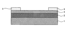
- FIG. 1 is a schematic cross-sectional view of a TFT element of the present invention.
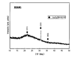
- FIG. 2 is a diagram showing the results of X-ray diffraction measurement of the oxide semiconductor thin film of Example 5.
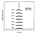
- FIG. 3 is a diagram showing the relationship between the heating temperature in the annealing treatment and the crystallization of the obtained oxide semiconductor thin film.
- the oxide semiconductor thin film of the present invention and a thin film transistor (TFT) using the oxide semiconductor thin film as a channel layer material will be described in detail.
- the crystalline oxide semiconductor thin film made of an oxide containing indium (In) and titanium (Ti) according to the present invention has a titanium content of 0. 0 by Ti / In atomic ratio. It is characterized by being in the range of 005 to 0.12. This makes it possible to achieve good carrier characteristics such as a carrier concentration of 1 ⁇ 10 19 cm ⁇ 3 or less, a carrier mobility of 1 cm 2 / Vsec or more, and further 3 cm 2 / Vsec or more.
- the carrier source of the crystalline oxide semiconductor thin film made of indium-only oxide that does not contain any additive elements is mainly oxygen deficient, but its formation is suppressed by adding titanium with high oxidation affinity. Is possible.
- titanium in the crystalline oxide semiconductor thin film becomes a tetravalent ion and acts as a donor, and thus can be a carrier source. Titanium behaves as a so-called ionized impurity scattering center and causes carrier scattering, so that the carrier mobility is lowered. Therefore, the crystalline oxide semiconductor thin film made of an oxide containing indium and titanium has a dominant effect of suppressing the generation of oxygen deficiency without increasing the carrier concentration as a carrier source more than necessary. It is necessary to control the titanium content within the above range so that ion scattering does not become excessive.
- the carrier concentration of the oxide semiconductor thin film exceeds 1 ⁇ 10 19 cm ⁇ 3 .
- the channel layer of the TFT preferably exhibits a lower carrier concentration and a higher carrier mobility.
- the titanium content is set at a Ti / In atomic ratio of 0.
- a carrier concentration of 5 ⁇ 10 17 cm ⁇ 3 or less and a carrier mobility of 5 cm 2 / Vsec or more can be achieved simultaneously.
- the oxide semiconductor thin film of the present invention is formed of an oxide composed of indium and titanium except for unavoidable impurities.
- a known additive element other than unavoidable impurities is appropriately added as a main component of indium and titanium. It can also be comprised by the oxide to contain.
- additive elements include gallium (Ga), aluminum (Al), chromium (Cr), iron (Fe), and tantalum (Ta).
- the content of these additive elements is preferably 0.0025 or less, more preferably 0.001 or less in terms of M / In atomic ratio, where M is the number of atoms of the additive element. If the content of the additive element exceeds 0.0025 in terms of the number ratio of M / In, desired characteristics cannot be obtained in relation to the contents of indium and titanium.
- the oxide semiconductor thin film of the present invention is crystalline and is substantially composed only of an indium oxide (In 2 O 3 ) phase having a bixbite structure. Is substantially not included.
- In the In 2 O 3 phase of the bixbite structure an InO 6 octahedral structure composed of indium and oxygen is formed, and adjacent InO 6 octahedral structures share a ridge, and the distance between In-In becomes shorter. Yes. For this reason, the overlapping of the orbits of electrons serving as carriers is large and the carrier mobility is improved.
- elements other than indium such as titanium and additive elements are dissolved in the In 2 O 3 layer having the bixbite type structure.
- an oxide semiconductor thin film of the present invention is configured only by the In 2 O 3 phase bixbyite structure
- the oxide semiconductor thin film characteristics are also included in the scope of the present invention, in addition to those having a crystal phase other than the In 2 O 3 phase shared by the InO 6 octahedral structure. Means included as long as possible. Note that the generation phase and structure of the oxide semiconductor thin film can be determined by X-ray diffraction measurement.
- the size of crystal grains constituting the oxide semiconductor thin film is preferably 10 nm or more, and preferably 20 nm or more. Is more preferable, and 50 nm or more is particularly preferable.
- the upper limit value of the average crystal grain size is not particularly limited, but is preferably 1000 nm or less from the viewpoint of making the distribution of crystal grain boundaries existing in the channel layer uniform.
- the average crystal grain size can be determined by, for example, calculation from the X-ray diffraction measurement result, image analysis of an SEM or EBSD observation image, and the like.
- the film thickness of the oxide semiconductor thin film of the present invention is preferably controlled in the range of 15 nm to 200 nm, more preferably 30 nm to 150 nm, and still more preferably 40 nm to 100 nm.
- oxide semiconductor thin film of the present invention when the film thickness is less than 15 nm, depending on the titanium content, even if annealing is performed at a high temperature of about 400 ° C. due to the influence of the substrate. In some cases, the amorphous oxide thin film as a precursor does not crystallize. Further, even if this oxide amorphous thin film is crystallized, sufficient crystallinity may not be obtained, or it may be difficult to make the average crystal grain size 10 nm or more. For this reason, high carrier mobility cannot be stably obtained in the obtained oxide semiconductor thin film.
- the influence on the crystallinity of the oxide semiconductor thin film due to the fact that the substrate is amorphous can be reduced by setting the thickness of the oxide semiconductor thin film to 30 nm or more. It becomes possible to eliminate the influence.
- the film thickness is preferably 200 nm or less, more preferably 150 nm or less, and even more preferably 100 nm or less. Note that by controlling the film thickness in the vicinity of 100 nm, when the oxide semiconductor thin film of the present invention is formed over a glass substrate, an improvement in the transmittance of blue light can be expected due to optical interference. Therefore, when applied to a transparent TFT, it is preferable to control the film thickness in the vicinity of 100 nm.
- the oxide semiconductor thin film of the present invention is made of an oxide containing indium and titanium, and is composed of a crystalline In 2 O 3 phase having a bixbite structure. For this reason, the TFT to which the oxide semiconductor thin film of the present invention is applied has high stability against external factors such as heat, and the negative light bias deterioration phenomenon hardly occurs.
- the carrier concentration is 1 ⁇ 10 19 cm ⁇ 3 or less and the carrier mobility is 1 cm by controlling the titanium content in the oxide semiconductor within a predetermined range. It regulates to become 2 / Vsec or more. By regulating the carrier concentration and the carrier mobility within such ranges, it can be applied as a material for a channel layer that requires a carrier concentration that is 2 to 4 digits lower than that of the transparent conductive film, and the high carrier mobility. Depending on the degree, it is possible to ensure high pixel control performance of the TFT.
- the carrier concentration of the channel layer is preferably regulated to 1 ⁇ 10 18 cm ⁇ 3 or less, more preferably 5 ⁇ 10 17 cm ⁇ 3 or less.
- the oxide semiconductor thin film of the present invention can realize such a low carrier concentration.
- the on / off ratio means the ratio of the resistance in the off state to the on state, and can be measured by a semiconductor parameter analyzer.
- the carrier mobility is less than 1 cm 2 / Vsec, it is difficult to ensure high pixel control performance of the TFT.
- the carrier mobility is preferably 3 cm 2 / Vsec or more, more preferably 5 cm 2 / Vsec or more.
- An oxide semiconductor thin film can realize such high carrier mobility.
- the oxide semiconductor thin film of the present invention can be obtained by sputtering, ion plating, etc., using an oxide sintered body target or tablet. It is formed on the substrate by a known film forming technique that can be applied. At this time, the composition ratio of the metal element of the oxide sintered body as a raw material can be appropriately set according to the film forming conditions. However, the composition ratio of the metal element of the oxide sintered body is the same as the composition ratio of the target oxide semiconductor thin film, and the film formation conditions are controlled so that the composition ratio is maintained. It can be said that it is an easy means.
- the composition ratio of the oxide sintered body is preferably the same as the composition ratio of the metal element of the target oxide semiconductor thin film. That is, the raw material of the oxide semiconductor thin film of the present invention is made of an oxide containing indium and titanium, and the titanium content is 0.005 to 0.12, preferably 0.01 to 0.1 in terms of the Ti / In atomic ratio. An oxide sintered body that is 0.06 is used.
- an oxide sintered body mainly composed of an In 2 O 3 phase having a bixbite structure is used.
- titanium is dissolved in the In 2 O 3 phase.
- In 2 O 3 phase titanium it is not dissolved, i.e., except for unavoidable impurities, any element also In 2 O 3 phase which is not dissolved may coexist.
- the crystal phase other than the In 2 O 3 phase is oxidized.
- An oxide sintered body dispersed in an indium sintered body can also be used as a raw material for targets and tablets.
- the area ratio of the crystal phase other than the In 2 O 3 phase to the In 2 O 3 phase must be 10% or less.
- the direct current power to be input is increased.
- the area ratio exceeds 10%, it is considered that a crystal phase other than the In 2 O 3 phase becomes a starting point of nodule growth as the sputtering progresses.
- the oxide sintered body used for forming the oxide semiconductor thin film of the present invention the area ratio of the crystal phase other than the In 2 O 3 phase is controlled to 10% or less, Since the crystal phase other than the In 2 O 3 phase is finely dispersed, the structure is unlikely to be a starting point for nodule growth.
- an oxide sintered body as a material for targets and tablets, even if the DC power input during film formation is increased, the generation of nodules is suppressed and abnormal discharge such as arcing is less likely to occur.
- An oxide semiconductor thin film can be formed efficiently.
- the oxide semiconductor thin film of the present invention can be formed by using a normal sputtering method or an ion plating method under the conditions usually selected by these methods.
- the direct current sputtering method is industrially advantageous because the thermal influence during film formation is small and high-speed film formation is possible. It is.
- a glass substrate is typical, but any substrate that can be used as a substrate for semiconductor devices such as silicon may be used.
- a resin film can be used as the substrate.
- the substrate temperature is preferably equal to or lower than the crystallization temperature of an amorphous film made of an oxide containing indium and titanium.
- the carrier concentration can be controlled to 1 ⁇ 10 19 cm ⁇ 3 or less, and further to 5 ⁇ 10 17 cm ⁇ 3 or less. It becomes difficult.
- the substrate temperature is preferably 200 ° C. or lower when the film thickness is in the range of 15 nm to 70 nm, and is preferably 100 ° C. or lower when the film thickness is in the range of 70 nm to 200 nm. In any case, it is more preferable that the temperature is in the range from room temperature to 100 ° C.
- film forming conditions are not particularly limited, and need to be appropriately selected according to a film forming method, a film forming apparatus, and the like.
- the sputtering gas is introduced into the chamber of the sputtering apparatus after evacuating the chamber to 2 ⁇ 10 ⁇ 4 Pa or less, and the gas pressure is set to 0. 1 Pa to 1 Pa, preferably 0.2 Pa to 0.8 Pa, more preferably 0.2 Pa to 0.5 Pa.
- the sputtering gas used at this time is preferably a mixed gas composed of an inert gas and oxygen, particularly argon and oxygen.
- the distance between the target and the substrate is adjusted to a range of 10 nm to 100 mm, preferably 40 nm to 70 mm, and the direct current power relative to the target area, that is, the direct current power density is in the range of about 1 W / cm 2 to 3 W / cm 2. It is preferable to apply direct current power to generate direct current plasma, perform pre-sputtering for 5 to 30 minutes, and then correct the substrate position if necessary and perform sputtering under the same conditions.
- the crystalline oxide semiconductor thin film is formed by heating the substrate during film formation to a temperature equal to or higher than the crystallization temperature of the oxide semiconductor thin film.
- Amorphous film is formed by controlling the film forming method and the substrate temperature from a room temperature to a relatively low temperature range of about 100 ° C., and then the amorphous film is annealed at a temperature higher than the crystallization temperature to be crystallized. The method of letting it be mentioned. In the present invention, any method can be adopted.
- the heating temperature in the annealing process can be set to 400 ° C. or lower regardless of which method is employed.
- the heating temperature is 250 ° C., preferably 300 ° C. or more, more preferably 350 ° C. This is necessary.
- the titanium content is controlled in the range of 0.005 to 0.12 in terms of the Ti / In atomic ratio, and in this case, the crystallization temperature of the oxide semiconductor thin film is about 220 ° C. For this reason, when the heating temperature is less than 250 ° C., the amorphous oxide semiconductor thin film cannot be sufficiently crystallized.
- heating temperature exceeds 450 degreeC carrier mobility may fall extremely, and this tendency begins to appear when the heating temperature exceeds 400 degreeC.
- the heating temperature is preferably 400 ° C. or lower.
- an annealing furnace can be used, and known means for annealing treatment can be widely used, and annealing conditions including a heating temperature corresponding to each means can be applied.
- the treatment time is preferably 1 minute to 120 minutes, more preferably 5 minutes to 60 minutes.
- the treatment time is less than 1 minute, the resulting oxide semiconductor thin film cannot be sufficiently crystallized.
- the effect beyond it cannot be expected and productivity will deteriorate.
- the annealing atmosphere is not limited, but can usually be performed in the air.
- an atmosphere containing oxygen is preferable, and the concentration is more preferably 20 vol% or more.
- JP 2010-251604 A as described above, a channel layer or the like is formed by a non-thermal sputtering method, and then in the atmosphere at 150 ° C. to 300 ° C. for 10 minutes to 120 minutes.
- a technique for reducing excessive defects in an amorphous film while maintaining an amorphous property by annealing is described.
- an annealing process within the above temperature range is performed by adding a considerable amount of an element that can be dissolved in the In 2 O 3 phase and increase the crystallization temperature. Is a technique that makes it possible to maintain the amorphous nature of the oxide semiconductor thin film, which is different from the present invention in this respect.
- the oxide semiconductor thin film of the present invention can be subjected to fine processing necessary for applications such as TFTs by wet etching or dry etching.
- processing by wet etching using a weak acid is performed. be able to.
- any weak acid can be used, but a weak acid containing succinic acid as a main component is preferable.
- a transparent conductive film etching solution ITO-06N manufactured by Kanto Chemical Co., Ltd. can be used.
- oxide thin films after crystallization and crystalline oxide thin films formed by setting the substrate temperature to the crystallization temperature or higher must be processed by dry etching using an appropriate etching gas. Can do.
- TFT Element The thin film transistor (TFT) of the present invention is characterized in that an oxide semiconductor thin film made of an oxide containing indium and titanium is applied to the channel layer material as described above.
- the structure of the TFT element of the present invention is not particularly limited.
- other forms such as a bottom gate / bottom contact type, a top gate / bottom contact type, and a top gate / top contact type may be selected. .
- the TFT element of FIG. 1 is composed of an oxide semiconductor thin film of the present invention and an Au / Ti laminated electrode on a SiO 2 / Si substrate on which a SiO 2 film is formed by thermal oxidation.
- the gate electrode 1 is composed of a Si substrate
- the gate insulating layer 2 is composed of a SiO 2 film
- the channel layer 3 is composed of an oxide semiconductor thin film of the present invention
- the source electrode 4 and the drain electrode 5 are composed of Au / Ti laminated electrodes.
- the substrate is not limited to this, and a substrate conventionally used as an electronic device substrate including a thin film transistor can also be used.
- a glass substrate such as non-alkali glass or quartz glass can be used in addition to the SiO 2 / Si substrate or the Si substrate.
- various metal substrates, plastic substrates, non-transparent heat-resistant polymer film substrates such as polyimide can be used.
- the gate electrode 1 is composed of a Si substrate.
- the present invention is not limited to this.
- metal thin films such as Mo, Al, Ta, Ti, Au, and Pt, and these metals
- the conductive oxide, nitride thin film or oxynitride thin film, or various conductive polymer materials can also be used.
- a transparent conductive film such as indium tin oxide (ITO) can be used.
- ITO indium tin oxide
- An oxide semiconductor thin film having the same composition as that of the oxide semiconductor thin film of the present invention can also be used as the transparent conductive film.
- the gate electrode 1 is required to have good conductivity.
- the specific resistance of these electrodes is preferably controlled in the range of 1 ⁇ 10 ⁇ 6 ⁇ ⁇ cm to 1 ⁇ 10 ⁇ 1 ⁇ ⁇ cm, and 1 ⁇ 10 ⁇ 6 ⁇ ⁇ cm to 1 More preferably, it is controlled within the range of ⁇ 10 ⁇ 3 ⁇ ⁇ cm.
- an insulating polymer such as a metal oxide thin film such as SiO 2 , Y 2 O 3 , Ta 2 O 5 , Hf oxide, a metal nitride thin film such as SiN x , or polyimide is used.
- Known materials such as materials can be used.
- the specific resistance of the gate insulating layer 2 is preferably in the range of 1 ⁇ 10 6 ⁇ ⁇ cm to 1 ⁇ 10 15 ⁇ ⁇ cm, and preferably 1 ⁇ 10 10 ⁇ ⁇ cm to 1 ⁇ 10 15 ⁇ ⁇ cm. Is more preferable.
- the specific resistance of the channel layer 3 is not particularly limited, but is preferably controlled to 10 ⁇ 1 ⁇ ⁇ cm to 10 6 ⁇ ⁇ cm, and particularly preferably 10 0 ⁇ ⁇ cm to 10 3 ⁇ ⁇ cm. More preferably, it is controlled.
- the amount of oxygen vacancies generated can be adjusted by selecting the film forming conditions of the sputtering method or the ion plating method and the annealing treatment conditions. For this reason, it is possible to achieve the specific resistance in the above range relatively easily.
- the source electrode 4 and the drain electrode 5 similarly to the gate electrode 1, a metal thin film such as Mo, Al, Ta, Ti, Au, Pt or the like, an alloy thin film of these metals, a conductive oxide or nitride of these metals
- a transparent conductive film such as ITO can be used for thin films, various conductive polymer materials, or transparent TFTs. Moreover, these thin films may be laminated.
- the source electrode 4 and the drain electrode 5 are required to have good conductivity. Specifically, the specific resistance of these electrodes is preferably in the range of 10 ⁇ 6 ⁇ ⁇ cm to 10 ⁇ 1 ⁇ ⁇ cm, more preferably in the range of 10 ⁇ 6 ⁇ ⁇ cm to 10 ⁇ 3 ⁇ ⁇ cm. To control.
- TFT element of this invention is demonstrated in detail.
- a method of annealing after low-temperature film formation will be described as an example when forming an oxide semiconductor thin film, but the TFT element of the present invention can adopt a method of forming a film at high temperature.
- it can be manufactured by appropriately combining known methods.
- a SiO 2 film is formed by thermal oxidation on the surface of a highly doped n-type Si wafer substrate to obtain a SiO 2 / Si substrate.
- an amorphous oxide semiconductor thin film having a predetermined film thickness is formed on the SiO 2 film of the substrate by DC magnetron sputtering.
- the film formation conditions at this time are the same as the conditions described in “2. Method for manufacturing oxide semiconductor thin film”, and thus the description thereof is omitted here.
- examples of a method for forming an oxide semiconductor thin film having a desired channel length and / or channel width include a method of performing etching using a photolithography technique or the like after the formation of the oxide semiconductor thin film as described above. be able to.
- a method of forming a film after masking at the time of forming the oxide semiconductor thin film can be employed.
- this oxide semiconductor thin film is annealed to turn the amorphous thin film into a crystalline oxide semiconductor thin film.
- the conditions for the annealing treatment are also the same as those described in “2. Method for manufacturing oxide semiconductor thin film”, and thus the description thereof is omitted here.
- the TFT element of the present invention can be obtained.
- a method of etching using a photolithography technique or the like after the formation of the Ti thin film and the Au thin film may be employed as in the formation of the channel layer.
- the oxide sintered body, the oxide semiconductor thin film, and the TFT element were evaluated by the following methods.
- the composition of the oxide semiconductor thin film obtained in each example and comparative example was measured by ICP emission spectroscopy. Further, the thickness of the oxide semiconductor thin film was measured with a surface shape measuring device (manufactured by KLA Tencor), and the film formation rate was calculated from the result and the film formation time. Furthermore, the carrier concentration and specific resistance of the oxide semiconductor thin film were measured with a Hall effect measuring device (manufactured by Toyo Technica Co., Ltd.), and the carrier mobility was calculated from these values. In addition, the production
- the characteristics evaluation of the TFT element was performed by confirming the operation of the TFT element, and measuring the on / off ratio and the field effect mobility using a semiconductor parameter analyzer (4200SCS manufactured by Keithley).
- the field effect mobility means an index related to high-speed operation of the TFT element.
- Example 1 An oxide sintered body (oxide sintered body target) made of indium oxide containing titanium (In 2 O 3 ) was prepared as a sputtering target. This oxide sintered body had a titanium content of 0.018 in terms of the Ti / In atomic ratio, and was constituted only by the In 2 O 3 phase.
- This oxide sintered body target was attached to a non-magnetic target cathode of a DC magnetron sputtering apparatus (manufactured by Tokki Co., Ltd.) having no arcing suppression function.
- a non-magnetic target cathode of a DC magnetron sputtering apparatus manufactured by Tokki Co., Ltd.
- an alkali-free glass substrate (Corning Corp., # 7059) was used, and the target-substrate distance was fixed to 60 mm. Then, after evacuating the chamber to 2 ⁇ 10 ⁇ 4 Pa or less, a mixed gas of Ar and O 2 is introduced so that the oxygen ratio is 6.0%, and the gas pressure is adjusted to 0.6 Pa. did.
- direct current power of 300 W (1.64 W / cm 2 ) was applied to generate direct current plasma to form an oxide semiconductor thin film.
- a substrate was placed at a stationary facing position of the sputtering target, and sputtering was performed without heating the substrate, whereby an oxide semiconductor thin film having a thickness of 50 nm was formed.
- ICP emission analysis it was confirmed that it was almost the same as the composition of the oxide sintered body.
- X-ray diffraction measurement it was confirmed that the oxide semiconductor thin film was amorphous.
- oxide semiconductor thin film after annealing is crystallized, and In 2 O 3 (222) is the main peak.
- This oxide semiconductor thin film has a substantially bixbyite structure. It was confirmed that it was composed of In 2 O 3 phase. Further, In 2 O 3 (222) it was calculated an average grain size than the peak was 50nm.
- the carrier concentration of the oxide semiconductor thin film was 3.0 ⁇ 10 17 cm ⁇ 3 and the carrier mobility was 12.3 cm 2 / Vsec. It was.
- Example 2 An amorphous oxide semiconductor thin film obtained in the same manner as in Example 1 was annealed in the atmosphere at 400 ° C. for 30 minutes. As a result of the X-ray diffraction measurement, the oxide semiconductor thin film after annealing is crystallized, and In 2 O 3 (222) is the main peak. This oxide semiconductor thin film has a substantially bixbyite structure. It was confirmed that it was composed of In 2 O 3 phase. The average crystal grain size was calculated from the In 2 O 3 (222) peak and found to be 59 nm. Furthermore, when the Hall effect of the oxide semiconductor thin film was measured, the carrier concentration of the oxide semiconductor thin film was 5.0 ⁇ 10 17 cm ⁇ 3 and the carrier mobility was 11.6 cm 2 / Vsec. .
- Example 3 An oxide semiconductor thin film was formed in the same manner as in Example 1 except that the Ti content of the oxide sintered compact target was 0.01 in terms of the Ti / In atomic ratio. As a result of measuring the composition of the obtained oxide semiconductor thin film by ICP emission analysis, it was confirmed that it was almost the same as the composition of the oxide sintered body. As a result of X-ray diffraction measurement, it was confirmed that the oxide semiconductor thin film was amorphous.
- this oxide semiconductor thin film was annealed under the same conditions as in Example 1.
- the oxide semiconductor thin film after annealing is crystallized, and In 2 O 3 (222) is the main peak.
- This oxide semiconductor thin film has a substantially bixbyite structure. It was confirmed that it was composed of In 2 O 3 phase. Further, the average crystal grain size was calculated from the In 2 O 3 (222) peak and found to be 58 nm.
- the carrier concentration of the oxide semiconductor thin film was 4.8 ⁇ 10 17 cm ⁇ 3 and the carrier mobility was 10.7 cm 2 / Vsec. .
- Example 4 An oxide semiconductor thin film was formed in the same manner as in Example 1 except that the Ti content of the oxide sintered compact target was 0.06 in terms of the Ti / In atomic ratio. As a result of measuring the composition of the obtained oxide semiconductor thin film by ICP emission analysis, it was confirmed that it was almost the same as the composition of the oxide sintered body. As a result of X-ray diffraction measurement, it was confirmed that the oxide semiconductor thin film was amorphous.
- this oxide semiconductor thin film was annealed under the same conditions as in Example 1.
- the oxide semiconductor thin film after annealing is crystallized, and In 2 O 3 (222) is the main peak.
- This oxide semiconductor thin film has a substantially bixbyite structure. It was confirmed that it was composed of In 2 O 3 phase. Further, In 2 O 3 (222) it was calculated an average grain size than was 55 nm.
- the carrier concentration of the oxide semiconductor thin film was 4.5 ⁇ 10 17 cm ⁇ 3 and the carrier mobility was 10.2 cm 2 / Vsec. .
- Example 5 An oxide semiconductor thin film was formed in the same manner as in Example 1 except that the titanium content of the oxide sintered compact target was 0.09 in terms of the Ti / In atomic ratio. As a result of measuring the composition of the obtained oxide semiconductor thin film by ICP emission analysis, it was confirmed that it was almost the same as the composition of the oxide sintered body. As a result of X-ray diffraction measurement, it was confirmed that the oxide semiconductor thin film was amorphous.
- this oxide semiconductor thin film was annealed under the same conditions as in Example 1.
- the oxide semiconductor thin film after annealing is crystallized, and In 2 O 3 (222) is the main peak.
- This oxide semiconductor thin film has a substantially bixbyite structure. It was confirmed that it was composed of In 2 O 3 phase. Further, In 2 O 3 (222) it was calculated an average grain size than was 55 nm. Further, when the Hall effect of the oxide semiconductor thin film was measured, the carrier concentration of the oxide semiconductor thin film was 4.7 ⁇ 10 17 cm ⁇ 3 and the carrier mobility was 5.2 cm 2 / Vsec. .
- Example 6 An amorphous oxide semiconductor thin film obtained in the same manner as in Example 5 was annealed in the atmosphere at 400 ° C. for 30 minutes. As a result of the X-ray diffraction measurement, the oxide semiconductor thin film after annealing is crystallized, and In 2 O 3 (222) is the main peak. This oxide semiconductor thin film has a substantially bixbyite structure. It was confirmed that it was composed of In 2 O 3 phase. Further, the average crystal grain size was calculated from In 2 O 3 (222) and found to be 58 nm. Further, when the Hall effect of the oxide semiconductor thin film was measured, the carrier concentration of the oxide semiconductor thin film was 3.9 ⁇ 10 17 cm ⁇ 3 and the carrier mobility was 6.0 cm 2 / Vsec. .
- Example 7 An oxide semiconductor thin film was formed in the same manner as in Example 1 except that the titanium content of the oxide sintered compact target was 0.005 in terms of the Ti / In atomic ratio. As a result of measuring the composition of the obtained oxide semiconductor thin film by ICP emission analysis, it was confirmed that it was almost the same as the composition of the oxide sintered body. As a result of X-ray diffraction measurement, it was confirmed that the oxide semiconductor thin film was amorphous.
- this oxide semiconductor thin film was annealed under the same conditions as in Example 1.
- the oxide semiconductor thin film after annealing is crystallized, and In 2 O 3 (222) is the main peak.
- This oxide semiconductor thin film has a substantially bixbyite structure. It was confirmed that it was composed of In 2 O 3 phase. Further, In 2 O 3 (222) it was calculated an average grain size than was 53 nm. Further, when the Hall effect of the oxide semiconductor thin film was measured, the carrier concentration of the oxide semiconductor thin film was 8.2 ⁇ 10 17 cm ⁇ 3 and the carrier mobility was 8.8 cm 2 / Vsec. .
- Example 8 An oxide semiconductor thin film was formed in the same manner as in Example 1 except that the titanium content of the oxide sintered compact target was 0.12 in terms of the Ti / In atomic ratio. As a result of measuring the composition of the obtained oxide semiconductor thin film by ICP emission analysis, it was confirmed that it was almost the same as the composition of the oxide sintered body. As a result of X-ray diffraction measurement, it was confirmed that the oxide semiconductor thin film was amorphous.
- this oxide semiconductor thin film was annealed under the same conditions as in Example 1.
- the oxide semiconductor thin film after annealing is crystallized, and In 2 O 3 (222) is the main peak.
- This oxide semiconductor thin film has a substantially bixbyite structure. It was confirmed that it was composed of In 2 O 3 phase. Further, In 2 O 3 (222) it was calculated an average grain size than was 54 nm.
- the carrier concentration of the oxide semiconductor thin film was 4.3 ⁇ 10 17 cm ⁇ 3 and the carrier mobility was 3.0 cm 2 / Vsec. .
- Example 9 An oxide semiconductor thin film was formed in the same manner as in Example 1 except that the film thickness was 15 nm. As a result of measuring the composition of the obtained oxide semiconductor thin film by ICP emission analysis, it was confirmed that it was almost the same as the composition of the oxide sintered body. As a result of X-ray diffraction measurement, it was confirmed that the oxide semiconductor thin film was amorphous.
- this oxide semiconductor thin film was annealed under the same conditions as in Example 1.
- the oxide semiconductor thin film after annealing is crystallized, and In 2 O 3 (222) is the main peak.
- This oxide semiconductor thin film has a substantially bixbyite structure. It was confirmed that it was composed of In 2 O 3 phase. Further, In 2 O 3 (222) it was calculated an average grain size than was 13 nm. Further, when the Hall effect of the oxide semiconductor thin film was measured, the carrier concentration of the oxide semiconductor thin film was 4.4 ⁇ 10 17 cm ⁇ 3 and the carrier mobility was 10.5 cm 2 / Vsec. .
- Example 10 An oxide semiconductor thin film was formed in the same manner as in Example 1 except that the film thickness was 200 nm. As a result of measuring the composition of the oxide semiconductor thin film by ICP emission analysis, it was confirmed that it was almost the same as the composition of the oxide sintered body. As a result of X-ray diffraction measurement, it was confirmed that the oxide semiconductor thin film was amorphous.
- this oxide semiconductor thin film was annealed under the same conditions as in Example 1.
- the oxide semiconductor thin film after annealing is crystallized, and In 2 O 3 (222) is the main peak.
- This oxide semiconductor thin film has a substantially bixbyite structure. It was confirmed that it was composed of In 2 O 3 phase. Further, In 2 O 3 (222) it was calculated an average grain size than was 71 nm.
- the carrier concentration of the oxide semiconductor thin film was 2.7 ⁇ 10 17 cm ⁇ 3 and the carrier mobility was 12.1 cm 2 / Vsec. .
- Example 1 An oxide semiconductor thin film was formed in the same manner as in Example 1 except that the titanium content of the oxide sintered compact target was 0.001 in terms of the Ti / In atomic ratio. As a result of measuring the composition of the obtained oxide semiconductor thin film by ICP emission analysis, it was confirmed that it was almost the same as the composition of the oxide sintered body. As a result of X-ray diffraction measurement, it was confirmed that the oxide semiconductor thin film was amorphous.
- this oxide semiconductor thin film was annealed under the same conditions as in Example 1.
- the oxide semiconductor thin film after annealing is crystallized, and In 2 O 3 (222) is the main peak.
- This oxide semiconductor thin film has a substantially bixbyite structure. It was confirmed that it was composed of In 2 O 3 phase. Further, In 2 O 3 (222) it was calculated an average grain size than was 55 nm.
- the carrier concentration of the oxide semiconductor thin film was 1.5 ⁇ 10 19 cm ⁇ 3 and the carrier mobility was 9.6 cm 2 / Vsec. .
- Example 2 An oxide semiconductor thin film was formed in the same manner as in Example 1 except that the titanium content of the oxide sintered compact target was 0.15 in terms of the Ti / In atomic ratio. As a result of measuring the composition of the obtained oxide semiconductor thin film by ICP emission analysis, it was confirmed that it was almost the same as the composition of the oxide sintered body. As a result of X-ray diffraction measurement, it was confirmed that the oxide semiconductor thin film was amorphous.
- this oxide semiconductor thin film was annealed under the same conditions as in Example 1.
- the oxide semiconductor thin film after annealing is crystallized, and In 2 O 3 (222) is the main peak.
- This oxide semiconductor thin film has a substantially bixbyite structure. It was confirmed that it was composed of In 2 O 3 phase. Further, In 2 O 3 (222) it was calculated an average grain size than was 50nm.
- the carrier concentration of the oxide semiconductor thin film was 1.3 ⁇ 10 19 cm ⁇ 3 and the carrier mobility was 0.84 cm 2 / Vsec. .
- Example 3 An amorphous oxide semiconductor thin film obtained in the same manner as in Example 1 was annealed in the atmosphere at 200 ° C. for 30 minutes. As a result of X-ray diffraction measurement, it was confirmed that this oxide semiconductor thin film was not crystallized and that no peak of any plane orientation of the In 2 O 3 phase was present. For this reason, the Hall effect of the oxide thin film was not measured.
- Example 2 An amorphous oxide semiconductor thin film obtained in the same manner as in Example 1 was separately prepared, and high temperature X-ray diffraction measurement was performed by a thin film X-ray method while heating and heating. As a result, it was confirmed that the range of the heating temperature at which crystallization of the oxide semiconductor thin film was confirmed was 205 ° C. to 210 ° C. (see FIG. 3).
- Examples 1 to 10 are examples in which the titanium content was controlled in the range of 0.005 to 0.12 in terms of the Ti / In atomic ratio, and annealing was performed at 400 ° C. or lower in the atmosphere. . Therefore, in all of Examples 1 to 10, the oxide semiconductor thin film was crystallized, and all of the average crystal grain size, carrier concentration, and carrier mobility were within the range defined in the present invention.
- the titanium content is controlled in the range of 0.01 to 0.06 in terms of the Ti / In atomic ratio, and annealing is performed at 400 ° C. or lower in the atmosphere. Therefore, it was confirmed that the carrier concentration was 5 ⁇ 10 17 cm ⁇ 3 or less and the carrier mobility was excellent carrier characteristics of 10 cm 2 / Vsec or more.
- the carrier concentration is 5 ⁇ 10 17. It was confirmed that the value was cm ⁇ 3 or less and the carrier mobility was 5 cm 2 / Vsec or more.
- Examples 7 and 8 are examples in which the titanium content is the lower limit value or the upper limit value. Although both the carrier concentration and the carrier concentration are within the range defined in the present invention, in Example 7, the carrier concentration is In Example 8, the carrier mobility showed a slightly inferior value compared to the other examples.
- Comparative Example 1 is an example in which the titanium content is less than 0.005 in terms of the Ti / In atomic ratio, that is, an example in which the titanium content is less than the lower limit.
- the carrier concentration is 1 ⁇ 10 19. It was confirmed that it exceeded cm ⁇ 3 .
- Comparative Example 2 is an example in which the titanium content exceeds 0.12 in terms of the Ti / In atomic ratio, that is, an example exceeding the upper limit value.
- the carrier concentration exceeds 1 ⁇ 10 19 cm ⁇ 3 .
- carrier mobility will be less than 1 cm ⁇ 2 > / Vsec.
- Comparative Example 3 is an example in which the heating temperature in the annealing treatment was 200 ° C., and the amorphous oxide semiconductor thin film could not be crystallized.
- Example 11 An oxide sintered body (oxide sintered body target) made of indium oxide containing titanium (In 2 O 3 ) was prepared as a sputtering target. This oxide sintered body had a titanium content of 0.018 in terms of the Ti / In atomic ratio, and was constituted only by the In 2 O 3 phase.
- the oxide sintered body target attached to the cathode for a non-magnetic body target of a DC magnetron sputtering apparatus without arcing control function, SiO 2 film which is thermally oxidized is formed, the Si wafer substrate having a thickness of 300 nm SiO 2
- An amorphous oxide semiconductor thin film was formed over the film so as to have a thickness of 50 nm.
- the film forming conditions at this time were the same as in Example 1.
- the oxide semiconductor thin film was crystallized by being annealed in the atmosphere at 300 ° C. for 30 minutes.
- the Si substrate, the SiO 2 film, and the crystalline oxide semiconductor thin film were used as the gate electrode 1, the gate insulating layer 2, and the channel layer 3, respectively.
- a Ti film having a thickness of 5 nm and an Au film having a thickness of 100 nm are sequentially formed on the surface of the channel layer 3 by direct current magnetron sputtering, and the source electrode 4 and the drain made of an Au / Ti laminated film are formed.
- the electrode 5 was formed to obtain a thin film transistor (TFT element) having the configuration shown in FIG. Note that the film formation conditions for the source electrode 4 and the drain electrode 5 were the same as the film formation conditions for the oxide semiconductor thin film except that the sputtering gas was argon (Ar) only and the DC power was changed to 50 W.
- the source electrode 4 and the drain electrode 5 were patterned using a metal mask to obtain a TFT element having a channel length of 100 ⁇ m and a channel width of 450 ⁇ m.
- the operating characteristics as the TFT element were confirmed.
- this TFT element showed good values of an on / off ratio of 108 or more and a field effect mobility of 22.5 cm 2 / Vsec.
Landscapes
- Engineering & Computer Science (AREA)
- Microelectronics & Electronic Packaging (AREA)
- Power Engineering (AREA)
- Chemical & Material Sciences (AREA)
- Physics & Mathematics (AREA)
- Condensed Matter Physics & Semiconductors (AREA)
- General Physics & Mathematics (AREA)
- Computer Hardware Design (AREA)
- Manufacturing & Machinery (AREA)
- Materials Engineering (AREA)
- Ceramic Engineering (AREA)
- Metallurgy (AREA)
- Chemical Kinetics & Catalysis (AREA)
- Mechanical Engineering (AREA)
- Organic Chemistry (AREA)
- Crystallography & Structural Chemistry (AREA)
- Thermal Sciences (AREA)
- Thin Film Transistor (AREA)
- Physical Vapour Deposition (AREA)
- Physical Deposition Of Substances That Are Components Of Semiconductor Devices (AREA)
Abstract
Priority Applications (3)
| Application Number | Priority Date | Filing Date | Title |
|---|---|---|---|
| KR1020157012834A KR20150088793A (ko) | 2012-11-22 | 2013-11-21 | 산화물 반도체 박막과 그의 제조 방법 및 박막 트랜지스터 |
| CN201380060993.5A CN104798205B (zh) | 2012-11-22 | 2013-11-21 | 氧化物半导体薄膜及其制造方法以及薄膜晶体管 |
| US14/646,869 US9368639B2 (en) | 2012-11-22 | 2013-11-21 | Oxide semiconductor thin film, production method thereof, and thin film transistor |
Applications Claiming Priority (2)
| Application Number | Priority Date | Filing Date | Title |
|---|---|---|---|
| JP2012-256866 | 2012-11-22 | ||
| JP2012256866A JP6107085B2 (ja) | 2012-11-22 | 2012-11-22 | 酸化物半導体薄膜および薄膜トランジスタ |
Publications (1)
| Publication Number | Publication Date |
|---|---|
| WO2014080996A1 true WO2014080996A1 (fr) | 2014-05-30 |
Family
ID=50776173
Family Applications (1)
| Application Number | Title | Priority Date | Filing Date |
|---|---|---|---|
| PCT/JP2013/081445 WO2014080996A1 (fr) | 2012-11-22 | 2013-11-21 | Film mince de semiconducteur à oxyde, procédé pour le produire et transistor à film mince |
Country Status (6)
| Country | Link |
|---|---|
| US (1) | US9368639B2 (fr) |
| JP (1) | JP6107085B2 (fr) |
| KR (1) | KR20150088793A (fr) |
| CN (1) | CN104798205B (fr) |
| TW (1) | TWI594433B (fr) |
| WO (1) | WO2014080996A1 (fr) |
Families Citing this family (7)
| Publication number | Priority date | Publication date | Assignee | Title |
|---|---|---|---|---|
| CN104319262B (zh) * | 2014-11-13 | 2017-02-01 | 京东方科技集团股份有限公司 | 一种多晶氧化物薄膜晶体管阵列基板及其制备方法 |
| CN106435491B (zh) * | 2015-08-06 | 2019-02-12 | 清华大学 | 溅射靶及氧化物半导体膜以及其制备方法 |
| JP2019124598A (ja) * | 2018-01-17 | 2019-07-25 | 住友金属鉱山株式会社 | 非晶質試料の結晶化温度測定方法および結晶化温度測定システム |
| JP7187775B2 (ja) * | 2018-01-17 | 2022-12-13 | 住友金属鉱山株式会社 | 非晶質試料の結晶化温度測定方法および結晶化温度測定システム |
| CN109378274B (zh) * | 2018-10-11 | 2022-04-22 | 吉林建筑大学 | 一种制备不同类型铟镓锌氧薄膜晶体管的方法 |
| KR20200072408A (ko) * | 2018-12-11 | 2020-06-22 | 한양대학교 산학협력단 | 인듐산화물층, 인듐 산화물층을 채널층으로 포함하는 박막트랜지스터, 및 박막트랜지스터의 제조방법 |
| JP7326795B2 (ja) * | 2019-03-20 | 2023-08-16 | 株式会社リコー | 電界効果型トランジスタ、表示素子、画像表示装置、及びシステム |
Citations (3)
| Publication number | Priority date | Publication date | Assignee | Title |
|---|---|---|---|---|
| JP2008192721A (ja) * | 2007-02-02 | 2008-08-21 | Bridgestone Corp | 薄膜トランジスタ及びその製造方法 |
| WO2008117739A1 (fr) * | 2007-03-23 | 2008-10-02 | Idemitsu Kosan Co., Ltd. | Dispositif semi-conducteur, film mince semi-conducteur polycristallin, procédé de fabrication d'un film mince semi-conducteur polycristallin, transistor à effet de champ, et procédé de fabrication d'un transistor à effet de champ. |
| JP2011146571A (ja) * | 2010-01-15 | 2011-07-28 | Idemitsu Kosan Co Ltd | In−Ga−O系酸化物焼結体、ターゲット、酸化物半導体薄膜及びこれらの製造方法 |
Family Cites Families (17)
| Publication number | Priority date | Publication date | Assignee | Title |
|---|---|---|---|---|
| US7141186B2 (en) * | 2002-10-29 | 2006-11-28 | Sumitomo Metal Mining Co., Ltd. | Oxide sintered body and sputtering target, and manufacturing method for transparent conductive oxide film as electrode |
| EP2246894B2 (fr) | 2004-03-12 | 2018-10-10 | Japan Science and Technology Agency | Oxyde amorphe et transistor à couche mince |
| US7646015B2 (en) | 2006-10-31 | 2010-01-12 | Semiconductor Energy Laboratory Co., Ltd. | Manufacturing method of semiconductor device and semiconductor device |
| WO2008114588A1 (fr) * | 2007-03-20 | 2008-09-25 | Idemitsu Kosan Co., Ltd. | Ice cible de pulvérisation, film semi-conducteur d'oxyde et dispositif semi-conducteur |
| US8461583B2 (en) * | 2007-12-25 | 2013-06-11 | Idemitsu Kosan Co., Ltd. | Oxide semiconductor field effect transistor and method for manufacturing the same |
| KR20130080063A (ko) | 2008-06-06 | 2013-07-11 | 이데미쓰 고산 가부시키가이샤 | 산화물 박막용 스퍼터링 타겟 및 그의 제조 방법 |
| JP2010045263A (ja) | 2008-08-15 | 2010-02-25 | Idemitsu Kosan Co Ltd | 酸化物半導体、スパッタリングターゲット、及び薄膜トランジスタ |
| JPWO2010032422A1 (ja) * | 2008-09-19 | 2012-02-02 | 出光興産株式会社 | 酸化物焼結体及びスパッタリングターゲット |
| US8445903B2 (en) | 2008-10-23 | 2013-05-21 | Idemitsu Kosan Co., Ltd. | Thin film transistor having a crystalline semiconductor film including indium oxide which contains a hydrogen element and method for manufacturing same |
| JP2010106291A (ja) | 2008-10-28 | 2010-05-13 | Idemitsu Kosan Co Ltd | 酸化物半導体及びその製造方法 |
| JP5553997B2 (ja) | 2009-02-06 | 2014-07-23 | 古河電気工業株式会社 | トランジスタおよびその製造方法 |
| JP2010251604A (ja) | 2009-04-17 | 2010-11-04 | Bridgestone Corp | 薄膜トランジスタの製造方法 |
| JP2010251606A (ja) | 2009-04-17 | 2010-11-04 | Bridgestone Corp | 薄膜トランジスタ |
| US20120037897A1 (en) | 2009-04-17 | 2012-02-16 | Bridgestone Corporation | Thin film transistor and method for manufacturing thin film transistor |
| WO2011016388A1 (fr) * | 2009-08-05 | 2011-02-10 | 住友金属鉱山株式会社 | Fritte d'oxyde, son procédé de production, film conducteur cible et transparent |
| CN102482156A (zh) * | 2009-09-30 | 2012-05-30 | 出光兴产株式会社 | In-Ga-Zn-O系氧化物烧结体 |
| JP5763064B2 (ja) * | 2010-06-02 | 2015-08-12 | 出光興産株式会社 | スパッタリングターゲット |
-
2012
- 2012-11-22 JP JP2012256866A patent/JP6107085B2/ja not_active Expired - Fee Related
-
2013
- 2013-11-21 CN CN201380060993.5A patent/CN104798205B/zh not_active Expired - Fee Related
- 2013-11-21 US US14/646,869 patent/US9368639B2/en not_active Expired - Fee Related
- 2013-11-21 WO PCT/JP2013/081445 patent/WO2014080996A1/fr active Application Filing
- 2013-11-21 KR KR1020157012834A patent/KR20150088793A/ko not_active Application Discontinuation
- 2013-11-22 TW TW102142591A patent/TWI594433B/zh not_active IP Right Cessation
Patent Citations (3)
| Publication number | Priority date | Publication date | Assignee | Title |
|---|---|---|---|---|
| JP2008192721A (ja) * | 2007-02-02 | 2008-08-21 | Bridgestone Corp | 薄膜トランジスタ及びその製造方法 |
| WO2008117739A1 (fr) * | 2007-03-23 | 2008-10-02 | Idemitsu Kosan Co., Ltd. | Dispositif semi-conducteur, film mince semi-conducteur polycristallin, procédé de fabrication d'un film mince semi-conducteur polycristallin, transistor à effet de champ, et procédé de fabrication d'un transistor à effet de champ. |
| JP2011146571A (ja) * | 2010-01-15 | 2011-07-28 | Idemitsu Kosan Co Ltd | In−Ga−O系酸化物焼結体、ターゲット、酸化物半導体薄膜及びこれらの製造方法 |
Also Published As
| Publication number | Publication date |
|---|---|
| JP6107085B2 (ja) | 2017-04-05 |
| US9368639B2 (en) | 2016-06-14 |
| CN104798205A (zh) | 2015-07-22 |
| JP2014107303A (ja) | 2014-06-09 |
| CN104798205B (zh) | 2018-01-05 |
| KR20150088793A (ko) | 2015-08-03 |
| TW201431077A (zh) | 2014-08-01 |
| US20150287830A1 (en) | 2015-10-08 |
| TWI594433B (zh) | 2017-08-01 |
Similar Documents
| Publication | Publication Date | Title |
|---|---|---|
| JP5966840B2 (ja) | 酸化物半導体薄膜および薄膜トランジスタ | |
| WO2014080996A1 (fr) | Film mince de semiconducteur à oxyde, procédé pour le produire et transistor à film mince | |
| JP6376153B2 (ja) | 酸化物半導体薄膜および薄膜トランジスタ | |
| WO2010032422A1 (fr) | Corps fritte d'oxyde et cible de pulverisation | |
| CN107924822B (zh) | 晶体氧化物半导体薄膜、晶体氧化物半导体薄膜的制造方法以及薄膜晶体管 | |
| WO2017150115A1 (fr) | Couche mince de semi-conducteur à oxyde, procédé de fabrication de couche mince de semi-conducteur à oxyde, et transistor à couches minces utilisant une couche mince de semi-conducteur à oxyde | |
| JP6036984B2 (ja) | 酸窒化物半導体薄膜 | |
| JP2016201458A (ja) | 微結晶質酸化物半導体薄膜及びそれを用いた薄膜トランジスタ | |
| JP2018104772A (ja) | 酸化物半導体薄膜の製造方法及び薄膜トランジスタの製造方法 | |
| JP2019021894A (ja) | 酸化物半導体薄膜の製造方法 | |
| JP2017168572A (ja) | 酸化物半導体薄膜、酸化物焼結体、薄膜トランジスタ及び表示装置 | |
| JP2019024058A (ja) | 酸化物半導体薄膜及び薄膜トランジスタの製造方法 | |
| JP2018135589A (ja) | 酸化物半導体薄膜及び薄膜トランジスタの製造方法 |
Legal Events
| Date | Code | Title | Description |
|---|---|---|---|
| 121 | Ep: the epo has been informed by wipo that ep was designated in this application |
Ref document number: 13856083 Country of ref document: EP Kind code of ref document: A1 |
|
| ENP | Entry into the national phase |
Ref document number: 20157012834 Country of ref document: KR Kind code of ref document: A |
|
| NENP | Non-entry into the national phase |
Ref country code: DE |
|
| WWE | Wipo information: entry into national phase |
Ref document number: 14646869 Country of ref document: US |
|
| 122 | Ep: pct application non-entry in european phase |
Ref document number: 13856083 Country of ref document: EP Kind code of ref document: A1 |