WO2014080941A1 - シンチレータパネルおよびその製造方法 - Google Patents
シンチレータパネルおよびその製造方法 Download PDFInfo
- Publication number
- WO2014080941A1 WO2014080941A1 PCT/JP2013/081279 JP2013081279W WO2014080941A1 WO 2014080941 A1 WO2014080941 A1 WO 2014080941A1 JP 2013081279 W JP2013081279 W JP 2013081279W WO 2014080941 A1 WO2014080941 A1 WO 2014080941A1
- Authority
- WO
- WIPO (PCT)
- Prior art keywords
- scintillator panel
- partition wall
- scintillator
- resin
- phosphor
- Prior art date
Links
Images
Classifications
-
- G—PHYSICS
- G01—MEASURING; TESTING
- G01T—MEASUREMENT OF NUCLEAR OR X-RADIATION
- G01T1/00—Measuring X-radiation, gamma radiation, corpuscular radiation, or cosmic radiation
- G01T1/16—Measuring radiation intensity
- G01T1/20—Measuring radiation intensity with scintillation detectors
- G01T1/2002—Optical details, e.g. reflecting or diffusing layers
-
- G—PHYSICS
- G21—NUCLEAR PHYSICS; NUCLEAR ENGINEERING
- G21K—TECHNIQUES FOR HANDLING PARTICLES OR IONISING RADIATION NOT OTHERWISE PROVIDED FOR; IRRADIATION DEVICES; GAMMA RAY OR X-RAY MICROSCOPES
- G21K4/00—Conversion screens for the conversion of the spatial distribution of X-rays or particle radiation into visible images, e.g. fluoroscopic screens
-
- G—PHYSICS
- G01—MEASURING; TESTING
- G01T—MEASUREMENT OF NUCLEAR OR X-RADIATION
- G01T1/00—Measuring X-radiation, gamma radiation, corpuscular radiation, or cosmic radiation
- G01T1/16—Measuring radiation intensity
- G01T1/20—Measuring radiation intensity with scintillation detectors
-
- G—PHYSICS
- G01—MEASURING; TESTING
- G01T—MEASUREMENT OF NUCLEAR OR X-RADIATION
- G01T1/00—Measuring X-radiation, gamma radiation, corpuscular radiation, or cosmic radiation
- G01T1/16—Measuring radiation intensity
- G01T1/20—Measuring radiation intensity with scintillation detectors
- G01T1/2018—Scintillation-photodiode combinations
- G01T1/20183—Arrangements for preventing or correcting crosstalk, e.g. optical or electrical arrangements for correcting crosstalk
-
- G—PHYSICS
- G01—MEASURING; TESTING
- G01T—MEASUREMENT OF NUCLEAR OR X-RADIATION
- G01T1/00—Measuring X-radiation, gamma radiation, corpuscular radiation, or cosmic radiation
- G01T1/16—Measuring radiation intensity
- G01T1/20—Measuring radiation intensity with scintillation detectors
- G01T1/202—Measuring radiation intensity with scintillation detectors the detector being a crystal
-
- G—PHYSICS
- G03—PHOTOGRAPHY; CINEMATOGRAPHY; ANALOGOUS TECHNIQUES USING WAVES OTHER THAN OPTICAL WAVES; ELECTROGRAPHY; HOLOGRAPHY
- G03F—PHOTOMECHANICAL PRODUCTION OF TEXTURED OR PATTERNED SURFACES, e.g. FOR PRINTING, FOR PROCESSING OF SEMICONDUCTOR DEVICES; MATERIALS THEREFOR; ORIGINALS THEREFOR; APPARATUS SPECIALLY ADAPTED THEREFOR
- G03F7/00—Photomechanical, e.g. photolithographic, production of textured or patterned surfaces, e.g. printing surfaces; Materials therefor, e.g. comprising photoresists; Apparatus specially adapted therefor
- G03F7/26—Processing photosensitive materials; Apparatus therefor
- G03F7/40—Treatment after imagewise removal, e.g. baking
Definitions
- the present invention relates to a scintillator panel used in a radiation detection apparatus used in a medical diagnostic apparatus, a nondestructive inspection instrument, and the like.
- X-ray images using films have been widely used in medical practice.
- digital radiation such as computed radiography (CR) and flat panel type radiation detectors (flat panel detector: FPD) has been used.
- Detection devices have been developed.
- a scintillator panel In a flat plate X-ray detector (FPD), a scintillator panel is used to convert radiation into visible light.
- the scintillator panel includes an X-ray phosphor such as cesium iodide (CsI), and the X-ray phosphor emits visible light according to the irradiated X-ray, and the light is emitted from a TFT (thin film transistor).
- X-ray information is converted into digital image information by converting it into an electrical signal using a CCD (charge-coupled device).
- CCD charge-coupled device
- Patent Documents 1 and 2 As a method for increasing the S / N ratio, there are a method of irradiating X-rays from the photodetector side (Patent Documents 1 and 2), and a partition wall in order to reduce the influence of scattering of visible light by the X-ray phosphor. There has been proposed a method of filling an X-ray phosphor in a cell partitioned by (Patent Documents 3 to 6).
- a method for forming such a partition wall conventionally used methods are a method of etching a silicon wafer, or a glass paste which is a mixture of a pigment or ceramic powder and a low-melting glass powder by a screen printing method. And a method of forming a partition wall by baking after pattern printing.
- the size of the scintillator panel that can be formed is limited by the size of the silicon wafer, and a large size such as a 500 mm square cannot be obtained.
- the multi-layer screen printing method using glass paste high-precision processing is difficult due to dimensional changes of the screen printing plate.
- the partition wall width is widened, the space between the partition walls is relatively narrow, the volume that can be filled with the X-ray phosphor is reduced, and the filling amount is not uniform.
- the scintillator panel obtained by this method has the drawbacks that the amount of X-ray phosphor is small, so that light emission is weak and uneven light emission occurs.
- Japanese Patent No. 3333278 JP 2001-330677 A Japanese Patent Laid-Open No. 5-60871 Japanese Patent Laid-Open No. 5-188148 JP 2011-188148 A JP 2011-007552 A
- barrier rib processing technology that can process large areas with high accuracy and narrow the barrier rib width, and visible light emitted by phosphors It is necessary to have a technology that efficiently guides the gas toward the detector without leaking to the outside of the partition wall.
- An object of the present invention is to solve the above problems and to provide a scintillator panel in which a narrow partition wall is formed with high accuracy in a large area, has high luminous efficiency, and realizes clear image quality.
- a scintillator panel having a flat substrate, a partition provided on the substrate, and a scintillator layer filled in a cell partitioned by the partition,
- the partition is made of a material mainly composed of a low-melting glass
- the binder resin is a resin selected from the group consisting of an acrylic resin, an epoxy resin, a polyester resin, a butyral resin, a polyamide resin, a silicone resin, and an ethyl cellulose resin.
- the partition wall is made of a material mainly composed of low-melting glass containing 2 to 20% by mass of an alkali metal oxide. .
- a step of applying a photosensitive paste containing a low-melting glass powder and a photosensitive organic component on a substrate to form a photosensitive paste coating film, and exposure for exposing the resulting photosensitive paste coating film A development step of dissolving and removing a portion of the photosensitive paste coating film after exposure that is soluble in the developer, and heating the developed photosensitive paste coating film pattern to a baking temperature of 500 to 700 ° C. to form an organic component And scintillator panel manufacturing method comprising: a firing step of softening and sintering low melting point glass to form barrier ribs, and a step of filling phosphors and binder resin into cells partitioned by the barrier ribs .
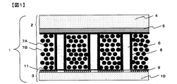
- FIG. 1 is a cross-sectional view schematically showing a configuration of a radiation detection apparatus including a scintillator panel of the present invention.
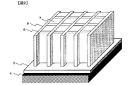
- FIG. 2 is a perspective view schematically showing a configuration of an example of the scintillator panel of the present invention.
- the radiation detection apparatus 1 includes a scintillator panel 2 and a photodetector 3.
- the scintillator panel 2 includes a scintillator layer 7 made of a phosphor 7A and a binder resin 7B, absorbs the energy of incident radiation such as X-rays, and emits electromagnetic waves having a wavelength in the range of 300 to 800 nm, that is, visible light.
- An electromagnetic wave (light) ranging from ultraviolet light to infrared light is emitted at the center.
- the scintillator panel 2 includes a flat scintillator panel side substrate 4, partition walls 6 formed thereon, and a scintillator layer 7 made of a phosphor and a binder resin filled in a space defined by the partition walls. Is done. A space defined by the partition walls 6 may be referred to as a cell.
- the radiation may be incident from either the scintillator panel side or the photodetector side.
- a radiation shielding layer 5 is preferably formed between the substrate on the side on which no radiation is incident and the partition wall. For example, since the scintillator panel 2 shown in FIG.
- the radiation shielding layer 5 absorbs the radiation that has passed through the scintillator layer 7 and can shield radiation leakage to the outside of the radiation detection apparatus.
- the radiation shielding layer 5 preferably has a high visible light reflectance.
- a reflective layer 8 is formed on the scintillator panel side substrate 4 or the radiation shielding layer 5.
- the photodetector 3 includes a photodetector-side substrate 10 and a photoelectric conversion layer 9 formed thereon.
- the substrate 10 for example, an insulating substrate such as a glass substrate, a ceramic substrate, or a resin substrate can be used.
- the photoelectric conversion layer 9 is a matrix in which photodetection pixels including photosensors such as photomultiplier tubes, photodiodes, PIN photodiodes, and the like, and thin film transistors (TFTs: Thin Film Transistors) are formed.
- the radiation detection apparatus 1 is configured by bonding a scintillator panel 2 and a photoelectric conversion layer 9 of a photodetector 3 so as to face each other.
- An adhesive layer 11 made of a polyimide resin or the like is preferably formed between the partition wall 6 and the scintillator layer 7 of the scintillator panel 2 and the photodetector 3.
- the radiation passes through the photoelectric conversion layer 9 and is then converted into visible light by the scintillator layer 7.
- the visible light is detected and photoelectrically converted by the photoelectric conversion layer 9. Is output.
- the partition wall 6 of the scintillator panel 2 is located in a portion between adjacent pixels in the photoelectric conversion layer 9.
- Each cell of the scintillator panel 2 is partitioned by a partition wall.
- each pixel of the photoelectric conversion layer can be associated with each cell of the scintillator panel. Even if the light emitted from the scintillator layer 7 is scattered by the phosphor, the scattered light is reflected by the partition walls, so that it is possible to prevent the scattered light from reaching the adjacent cell. Image blur can be reduced, and high-accuracy shooting is possible.
- a reflective layer 8 on the surface of the partition wall 6.
- the light emitted from the phosphor in the cell can be efficiently guided to the photodetector 3. It is also preferable to form the reflective layer 8 only on one side surface of the partition wall 6. The light emitted from the phosphor in the cell is reflected by the reflection layer 8 and therefore does not pass to the adjacent cell. Therefore, high-accuracy shooting is possible.
- the partition wall on which the reflective layer is not formed transmits light, the light reaching the partition wall on the side where the reflective layer is not formed passes through the partition wall, but is formed on the opposite side surface. Therefore, it is not transmitted to the adjacent cell.
- the partition preferably has a high light transmittance, and more preferably a partition having a light transmittance of 550 nm at a thickness of 30 ⁇ m in the range of 10 to 100%.
- the material of the scintillator panel side substrate 4 is preferably a material having high radiation transparency, and various types of glass, polymer materials, metals, and the like can be used.
- plate glass made of glass such as quartz, borosilicate glass, chemically tempered glass
- ceramic substrate made of ceramic such as sapphire, silicon nitride, silicon carbide
- semiconductor such as silicon, germanium, gallium arsenide, gallium phosphide, gallium nitrogen
- semiconductor substrate comprising: cellulose acetate film, polyester film, polyethylene terephthalate film, polyamide film, polyimide film, triacetate film, polycarbonate film, carbon fiber reinforced resin sheet and other polymer films (plastic film); aluminum sheet, iron sheet, copper
- a metal sheet such as a sheet; a metal sheet having a metal oxide coating layer, an amorphous carbon substrate, or the like can be used.
- a plastic film and a plate glass are preferable in terms of flatness
- the scintillator panel side substrate 4 may be made of a material having a radiation transmissive material, but the radiation to the outside of the radiation detection apparatus may be used.
- a substrate made of a radiation shielding material that is, a radiation shielding substrate.
- the radiation shielding substrate include a metal plate such as an iron plate or a lead plate, or a glass plate or film containing a heavy metal such as iron, lead, gold, silver, copper, platinum, tungsten, bismuth, tantalum, or molybdenum. It is done.
- the radiation shielding layer 5 is formed between the substrate on which radiation is not incident and the partition wall 6, the necessity that the scintillator panel side substrate 4 is a radiation shielding substrate is reduced.
- Examples of the material of the radiation shielding layer 5 include materials capable of absorbing radiation such as glass or ceramics containing heavy metals such as iron, lead, gold, silver, copper, platinum, tungsten, bismuth, tantalum or molybdenum. .
- the radiation shielding layer 5 is formed, for example, by applying a radiation shielding layer paste in which an organic component and an inorganic powder containing the above-described material are dispersed in a solvent and drying the coating on a substrate, which is preferably 500 to 700. It can be formed by firing at a temperature of ° C, more preferably 500 to 650 ° C.
- the radiation shielding layer and the partition it is preferable to fire the radiation shielding layer and the partition at the same time because the number of steps is reduced.
- it contains a polymerizable monomer, a polymerizable oligomer or a polymerizable polymer that is an organic component of the radiation shielding layer paste, and a thermal polymerization initiator. It is also preferable to use a thermosetting organic component to form and heat cure after forming a coating film.
- the partition walls must be made of a material mainly composed of low-melting glass from the viewpoint of durability, heat resistance and high-definition processing. It is preferably made of a material mainly composed of low melting point glass containing 2 to 20% by mass of an alkali metal oxide.
- a material mainly composed of a low melting point glass containing 2 to 20% by mass of an alkali metal oxide has an appropriate refractive index and softening temperature, and is suitable for forming a narrow partition wall in a large area with high accuracy. ing.
- the low melting point glass means a glass having a softening temperature of 700 ° C. or lower.
- the main component is a low-melting glass containing 2 to 20% by mass of an alkali metal oxide, which means that 50 to 100% by mass of the material constituting the partition contains 2 to 20% by mass of the alkali metal oxide.
- the low melting point glass is preferably made of a material mainly composed of low melting point glass containing 2 to 20% by mass of an alkali metal oxide.
- the scintillator panel manufacturing method applies a photosensitive paste containing a low-melting glass and a photosensitive organic component on a substrate in order to process a large area with high accuracy and reduce the width of the partition wall.
- a process for forming a paste coating film, an exposure process for exposing the resulting photosensitive paste coating film, a developing process for dissolving and removing a soluble portion of the photosensitive paste coating film after the exposure, and a photosensitivity after development The paste coating film pattern is heated to a firing temperature of 500 to 700 ° C. to remove organic components and soften and sinter low-melting glass to form partition walls, and a metal reflective layer is formed on the surface of the partition walls. And a step of filling the phosphor and the binder resin in the cells partitioned by the partition walls.
- a necessary portion of the photosensitive paste coating film is photocured by exposure, or an unnecessary portion of the photosensitive paste coating film is photodecomposed, so that the dissolution contrast of the photosensitive paste coating film with respect to the developer is increased.
- the portion of the photosensitive paste coating film after exposure that is soluble in the developer is removed with the developer, and a photosensitive paste coating film pattern in which only necessary portions remain is obtained.
- the resulting photosensitive paste coating film pattern is fired at a temperature of 500 to 700 ° C., preferably 500 to 650 ° C., whereby organic components are decomposed and removed, and the low-melting glass is softened and removed. Sintered to form barrier ribs containing low melting glass.
- the firing temperature is preferably 500 ° C. or higher.
- the firing temperature exceeds 700 ° C., when a general glass substrate is used as the substrate, deformation of the substrate becomes large, and therefore the firing temperature is preferably 700 ° C. or less.
- This method makes it possible to form partition walls with higher accuracy than the method of firing after laminating glass paste by multilayer screen printing.
- the photosensitive paste is preferably composed of a photosensitive organic component and an inorganic powder containing a low melting point glass containing 2 to 20% by mass of an alkali metal oxide.
- the organic component needs a certain amount to form the photosensitive paste coating film pattern before firing, but if there is too much organic component, the amount of the substance to be removed in the firing process increases and the firing shrinkage ratio is large. Therefore, pattern defects are likely to occur in the firing process.
- the organic component is too small, the mixing and dispersibility of the inorganic fine particles in the paste will be reduced, so that not only will defects easily occur during firing, but the applicability of the paste will decrease due to an increase in paste viscosity.
- the stability of the paste is also adversely affected, which may be undesirable.
- the content of the inorganic powder in the photosensitive paste is preferably 30 to 80% by mass, and more preferably 40 to 70% by mass.
- the ratio of the low melting point glass to the whole inorganic powder is preferably 50 to 100% by mass. If the low melting point glass is less than 50% by mass of the inorganic powder, sintering does not proceed well in the firing step, and the strength of the resulting partition wall is reduced, which is not preferable.
- a glass powder made of a low-melting glass having a softening temperature of 480 ° C. or higher as a low-melting glass to be used Is preferably used.
- the softening temperature is less than 480 ° C.
- the low-melting glass is softened before the organic component is sufficiently removed during firing, and the organic component residue is taken into the glass.
- the residue of the organic component taken in into glass becomes a factor of coloring of glass.
- the firing temperature in the firing step needs to be 500 to 700 ° C., and preferably 500 to 650 ° C. Therefore, the softening temperature of the low-melting glass is preferably 480 to 680 ° C., and 480 to 620 ° C. Is more preferable.
- the softening temperature is determined by calculating the endothermic temperature at the endothermic peak from the DTA curve obtained by measuring the sample using a differential thermal analyzer (DTA, “Differential Differential Thermal Balance TG8120” manufactured by Rigaku Corporation). Obtained by extrapolation. Specifically, using a differential thermal analyzer, the temperature is increased from room temperature to 20 ° C./min using alumina powder as a standard sample, and the inorganic powder as a measurement sample is measured to obtain a DTA curve. The softening point Ts obtained by extrapolating the endothermic end temperature at the endothermic peak from the obtained DTA curve by the tangent method is defined as the softening temperature.
- DTA differential Thermal analyzer
- the alkali metal refers to lithium, sodium, potassium, rubidium and cesium, but the alkali metal oxide used in the present invention is a metal oxide selected from the group consisting of lithium oxide, sodium oxide and potassium oxide. Say things.
- the content X (M 2 O) of the alkali metal oxide in the low-melting glass is preferably in the range of 2 to 20% by mass. If the content of the alkali metal oxide is less than 2% by mass, the softening temperature becomes high, and thus the firing step needs to be performed at a high temperature. For this reason, when a glass substrate is used as the substrate, the substrate is deformed in the baking process, and thus the resulting scintillator panel is likely to be distorted or defects in the partition walls are easily generated. Moreover, when content of an alkali metal oxide exceeds 20 mass%, the viscosity of glass will fall too much in a baking process. Therefore, the shape of the obtained partition wall is likely to be distorted. Moreover, when the porosity of the obtained partition wall becomes too small, the light emission luminance of the obtained scintillator panel is lowered.
- the alkali metal oxide it is preferable to add 3 to 10% by mass of zinc oxide in order to adjust the viscosity of the glass at a high temperature.
- the content of zinc oxide is less than 3% by mass, the viscosity of the glass at a high temperature tends to increase.
- the content of zinc oxide exceeds 10% by mass, the cost of glass tends to increase.
- the low melting point glass contains silicon oxide, boron oxide, aluminum oxide, or an alkaline earth metal oxide, etc., thereby stabilizing the low melting point glass.
- the crystallinity, transparency, refractive index, thermal expansion characteristic, etc. can be controlled.
- the composition of the low-melting glass is preferably set to the composition range shown below because a low-melting glass having viscosity characteristics suitable for the present invention can be produced.
- Alkali metal oxide 2 to 20% by mass Zinc oxide: 3-10% by mass Silicon oxide: 20-40% by mass Boron oxide: 25-40% by mass Aluminum oxide: 10-30% by mass Alkaline earth metal oxide: 5 to 15% by mass
- the alkaline earth metal is one or more metals selected from the group consisting of magnesium, calcium, barium and strontium.
- the particle diameter of the inorganic particles including the low melting point glass can be evaluated using a particle size distribution measuring apparatus (“MT3300” manufactured by Nikkiso Co., Ltd.).
- MT3300 manufactured by Nikkiso Co., Ltd.
- As a measuring method an inorganic powder is put into a sample chamber filled with water, and measurement is performed after ultrasonic treatment for 300 seconds.
- the particle size of the low melting point glass is preferably 50% volume average particle size (D50) of 1.0 to 4.0 ⁇ m.
- D50 volume average particle size
- the particle size of the low melting point glass is preferably 50% volume average particle size (D50) of 1.0 to 4.0 ⁇ m.
- D50 volume average particle size
- the aggregation of particles becomes strong, it becomes difficult to obtain uniform dispersibility, and the fluidity stability of the paste tends to be low. In such a case, when the paste is applied, the thickness uniformity of the coating film decreases.
- D50 exceeds 4.0 ⁇ m, the surface unevenness of the obtained sintered body becomes large, and the pattern tends to be crushed in a subsequent process.
- the photosensitive paste may contain, as a filler, high-melting glass that does not soften at 700 ° C. or ceramic particles such as silicon oxide, aluminum oxide, titanium oxide, or zirconium oxide in addition to the low-melting glass described above.
- a filler high-melting glass that does not soften at 700 ° C.
- ceramic particles such as silicon oxide, aluminum oxide, titanium oxide, or zirconium oxide in addition to the low-melting glass described above.
- the filler preferably has an average particle size of 0.5 to 4.0 ⁇ m for the same reason as the low melting point glass.
- the refractive index n1 of the low-melting glass and the refractive index n2 of the organic component preferably satisfy ⁇ 0.1 ⁇ n1-n2 ⁇ 0.1, and ⁇ 0.01 ⁇ n1-n2 ⁇ 0. It is more preferable to satisfy 01, and it is further preferable to satisfy ⁇ 0.005 ⁇ n1 ⁇ n2 ⁇ 0.005. By satisfying this condition, light scattering at the interface between the low-melting glass and the organic component is suppressed in the exposure process, and a highly accurate pattern can be formed. By adjusting the compounding ratio of the oxide constituting the low-melting glass, a low-melting glass having preferable thermal characteristics and a preferable refractive index can be obtained.
- the refractive index of the low melting point glass can be measured by the Becke line detection method.
- the refractive index at a wavelength of 436 nm (g line) at 25 ° C. was defined as the refractive index of the low-melting glass.
- the refractive index of an organic component can be calculated
- the refractive index at a wavelength of 436 nm (g line) at 25 ° C. was defined as the refractive index of the photosensitive organic component.
- the photosensitive paste contains a photosensitive organic component as an organic component, and can be patterned by the photosensitive paste method as described above.
- the reactivity can be controlled by using a photosensitive monomer, photosensitive oligomer, photosensitive polymer, photopolymerization initiator, or the like as the photosensitive organic component.
- the photosensitivity in the photosensitive monomer, photosensitive oligomer and photosensitive polymer means that when the paste is irradiated with actinic rays, the photosensitive monomer, photosensitive oligomer or photosensitive polymer is photocrosslinked, photopolymerized. It means that the chemical structure is changed by causing the reaction.
- the photosensitive monomer is a compound having an active carbon-carbon double bond, and examples thereof include monofunctional compounds and polyfunctional compounds having a vinyl group, acryloyl group, methacryloyl group or acrylamide group as a functional group.
- a compound selected from the group consisting of a polyfunctional acrylate compound and a polyfunctional methacrylate compound containing 10 to 80% by mass in the organic component increases the crosslink density at the time of curing by photoreaction, and improves the pattern formability. It is preferable in terms of improvement. Since various types of compounds have been developed as the polyfunctional acrylate compound and the polyfunctional methacrylate compound, it is possible to appropriately select them from the viewpoint of reactivity, refractive index, and the like.
- Photosensitive oligomers or photosensitive polymers include, for example, acrylic acid, methacrylic acid, itaconic acid, crotonic acid, maleic acid, fumaric acid, vinyl acetic acid or their anhydrides and other carboxyl group-containing monomers and methacrylic acid esters, acrylic acid. It can be obtained by copolymerizing monomers such as ester, styrene, acrylonitrile, vinyl acetate or 2-hydroxyacrylate.
- an ethylenic group having a glycidyl group or an isocyanate group with respect to a mercapto group, amino group, hydroxyl group or carboxyl group in the oligomer or polymer is used.
- a method in which a saturated compound, a carboxylic acid such as acrylic acid chloride, methacrylic acid chloride or allyl chloride, or maleic acid is reacted can be used.
- the photopolymerization initiator is a compound that generates radicals upon irradiation with actinic rays.
- Specific examples include benzophenone, methyl o-benzoylbenzoate, 4,4-bis (dimethylamino) benzophenone, 4,4-bis (diethylamino) benzophenone, 4,4-dichlorobenzophenone, 4-benzoyl-4-methyl.
- the photosensitive paste can contain a copolymer having a carboxyl group as a binder.
- Copolymers having a carboxyl group include, for example, acrylic acid, methacrylic acid, itaconic acid, crotonic acid, maleic acid, fumaric acid, vinyl acetic acid or their anhydrides and other carboxyl group-containing monomers and methacrylic acid esters, acrylic acid.
- Other monomers such as ester, styrene, acrylonitrile, vinyl acetate or 2-hydroxy acrylate are selected and copolymerized using an initiator such as azobisisobutyronitrile.
- a copolymer having acrylic acid ester or methacrylic acid ester and acrylic acid or methacrylic acid as a copolymerization component is preferably used since the thermal decomposition temperature at the time of firing is low.
- the photosensitive paste becomes a paste excellent in solubility in an alkaline aqueous solution by containing a copolymer having a carboxyl group.
- the acid value of the copolymer having a carboxyl group is preferably 50 to 150 mgKOH / g.
- an acid value shall be 50 mgKOH / g or more. Therefore, it is not necessary to increase the concentration of the developing solution, and it is possible to prevent peeling of the exposed portion and obtain a high-definition pattern.
- the copolymer having a carboxyl group has an ethylenically unsaturated group in the side chain.
- the ethylenically unsaturated group include an acryl group, a methacryl group, a vinyl group, and an allyl group.
- the photosensitive paste is prepared by adding an organic solvent and a binder to a photosensitive organic component comprising a low-melting glass and a photosensitive monomer, photosensitive oligomer, photosensitive polymer, photopolymerization initiator, etc. After preparing the composition, it is mixed and dispersed homogeneously with three rollers or a kneader.
- the viscosity of the photosensitive paste can be appropriately adjusted depending on the addition ratio of inorganic powder, thickener, organic solvent, polymerization inhibitor, plasticizer, anti-settling agent, etc., but the range is preferably 2 to 200 Pa ⁇ s. .
- a viscosity of 2 to 5 Pa ⁇ s is preferable.
- a viscosity of 50 to 200 Pa ⁇ s is preferable.
- a viscosity of 10 to 50 Pa ⁇ s is preferable.
- a partition wall can be formed by applying the photosensitive paste thus obtained onto a substrate, forming a desired pattern by a photolithography method, and further baking.
- the barrier rib is manufactured using the photosensitive paste by a photolithography method
- the present invention is not limited to this.
- a photosensitive paste coating film is formed by coating a photosensitive paste on the entire surface or partially on the substrate so that the height after firing is the desired partition wall height.
- a coating method methods such as a screen printing method, a bar coater, a roll coater, a die coater, or a blade coater can be used.
- the coating thickness can be adjusted by selecting the number of coatings, screen mesh, paste viscosity, and the like.
- an exposure process is performed.
- a method of exposing through a photomask is common, as is done in normal photolithography.
- the photosensitive paste coating film is exposed through a photomask having openings corresponding to the partition pattern to be obtained.
- a proximity exposure machine or the like can be used as the exposure apparatus.
- when performing exposure of a large area after apply
- the actinic rays used for exposure include near infrared rays, visible rays, and ultraviolet rays.
- ultraviolet rays are preferable.
- the light source for example, a low-pressure mercury lamp, a high-pressure mercury lamp, an ultra-high pressure mercury lamp, a halogen lamp or a germicidal lamp can be used, and an ultra-high pressure mercury lamp is preferable.
- the exposure conditions vary depending on the thickness of the photosensitive paste coating film, the exposure is usually performed for 0.01 to 30 minutes using an ultrahigh pressure mercury lamp with an output of 1 to 100 mW / cm 2 .
- development is performed using the difference in solubility in the developer between the exposed and unexposed portions of the photosensitive paste coating film, and the soluble portion of the photosensitive paste coating film soluble in the developer is dissolved and removed.
- a grid-like or stripe-like photosensitive paste coating film pattern is obtained.
- Development is performed by dipping, spraying or brushing.
- a solvent that can dissolve the organic components in the paste can be used for the developer.
- the developer is preferably composed mainly of water. When a compound having an acidic group such as a carboxyl group is present in the paste, development can be performed with an alkaline aqueous solution.
- an inorganic alkaline aqueous solution such as sodium hydroxide, sodium carbonate or calcium hydroxide can be used.
- an organic alkaline aqueous solution because an alkaline component can be easily removed during firing.
- the organic alkali include tetramethylammonium hydroxide, trimethylbenzylammonium hydroxide, monoethanolamine and diethanolamine.
- the concentration of the alkaline aqueous solution is preferably 0.05 to 5% by mass, and more preferably 0.1 to 1% by mass.
- the development temperature at the time of development is preferably 20 to 50 ° C. for process control.
- a firing process is performed in a firing furnace.
- the atmosphere and temperature of the firing process vary depending on the type of the photosensitive paste and the substrate, but firing is performed in air, nitrogen, hydrogen, or the like.
- the firing furnace a batch-type firing furnace or a belt-type continuous firing furnace can be used.
- the firing is preferably carried out by holding at a temperature of 500 to 700 ° C. for 10 to 60 minutes.
- the firing temperature is more preferably 500 to 650 ° C.
- a reflective layer is formed.
- the method for forming the reflective layer is not particularly limited, and various film forming methods such as a method of applying a paste containing a reflective material and then baking and removing the solvent, a method of spraying the paste by spraying, and a plating method are utilized. can do.
- a vacuum film forming method such as vapor deposition, sputtering, ion plating, CVD, or laser ablation is preferable because a uniform reflective layer can be formed at a lower temperature, and sputtering is more preferable because a uniform film can be formed on the side wall of the partition wall.
- the temperature during the formation of the reflective layer is preferably lower than the temperature during the formation of the partition.
- the material of the reflective layer is not particularly limited, but it is preferable to use a material that reflects visible light that is an electromagnetic wave having a wavelength of 300 to 800 nm emitted from the phosphor. Among them, metals or metal oxides such as silver, gold, aluminum, nickel or titanium with little deterioration are preferable.
- the reflection layer preferably has a reflectance of 60% or more, more preferably 80% or more, of the emitted light having a wavelength of 550 nm in order to efficiently use the emitted light of the phosphor.
- the reflective layer When forming the reflective layer only on one side surface of the partition wall, for example, a method of inclining the substrate by 45 degrees or more with respect to the metal sputtering target in the sputtering method, or masking the side surface not forming the reflective layer with a resin or the like And a method of forming a reflective layer from the substrate and then removing the masking material.
- the reflective layer can be formed only on one side surface of the partition wall.
- a method for forming the reflective layer only in a specific cell for example, a reflective layer paste containing a reflective layer powder, an organic binder, and an organic solvent as main components is prepared, applied to the target cell, and dried. And the method of baking as needed is mentioned.
- a method of applying the reflective layer paste in the cell for example, a screen printing method for pattern printing using a screen printing plate, a dispenser method for applying a reflective layer paste from the tip of a discharge nozzle, or an inkjet Law.
- a photosensitive paste method may be used in which a photosensitive reflective layer paste containing a photosensitive organic component is applied to the entire surface, and then the unnecessary portions of the photosensitive reflective layer paste are removed by exposure and development.
- the dispenser method is preferable from the viewpoint of productivity.
- a light shielding layer is formed between the partition wall and the reflective layer. More preferably, a light shielding layer is formed on the surface of the reflective layer, and further a reflective layer is formed on the surface of the light shielding layer.
- the material of the light shielding layer is not particularly limited, and a metal film such as chromium, nichrome or tantalum, a resin containing a black pigment such as carbon, or the like can be used.
- a method for forming the light shielding layer is not particularly limited, and a method of applying a paste containing a light shielding material and various vacuum film forming methods can be used.
- the partition wall height H1 is preferably 100 to 3000 ⁇ m, more preferably 150 to 500 ⁇ m.
- H1 exceeds 3000 ⁇ m, the workability when forming the partition walls is lowered.
- H1 is less than 100 ⁇ m, the amount of phosphor that can be filled is reduced, and the light emission luminance of the scintillator panel obtained is lowered.
- the interval P1 between adjacent partition walls is preferably 30 to 1000 ⁇ m.
- P1 is less than 30 ⁇ m, workability when forming the partition walls is lowered.
- P1 is too large, the accuracy of the image of the scintillator panel obtained will become low.
- the partition wall height H1 is preferably larger than the partition wall spacing P1. This is because by increasing the partition wall, the amount of phosphor filled increases and the light emission luminance improves.
- the partition wall width is preferably such that the width (bottom width) L2 of the interface between the partition wall and the substrate is larger than the width L1 of the top (detector side) of the partition wall.
- the bottom width L2 is preferably 10 to 150 ⁇ m, and the top width L1 is preferably 5 to 80 ⁇ m. If L2 is less than 10 ⁇ m, defects in the partition walls are likely to occur during firing. On the other hand, when L2 is larger than 150 ⁇ m, the amount of phosphor that can be filled in the space partitioned by the partition walls is reduced. Moreover, the intensity
- the aspect ratio (H1 / L2) of H1 to L2 is preferably 1.0 to 25.0.
- the aspect ratio (H1 / P1) of H1 to P1 is preferably 1.0 to 3.5.
- the partition wall height H1 and the partition wall spacing P1 can be measured by exposing a partition wall cross section perpendicular to the substrate and observing the cross section with a scanning electron microscope (for example, “S4600” manufactured by Hitachi, Ltd.).
- the width of the partition wall at the contact portion between the partition wall and the substrate is L2.
- the width of the partition wall at the contact portion between the partition wall and the shielding layer is L2.
- the width of the topmost part of the partition wall is L1. If the top of the partition wall is rounded or the bottom of the partition wall is skirted and it is difficult to accurately grasp the top of the partition wall or the bottom of the partition wall, the height of the partition wall is 90% higher than L1.
- L10 is the line width of the portion of the portion from the partition wall bottom surface when H1 is 100.
- the scintillator panel can be completed by filling the phosphor and binder resin into the cells partitioned by the partition walls.
- the cell refers to a space partitioned by grid-like or stripe-like partition walls.
- the phosphor and binder resin filled in the cell are referred to as a scintillator layer.
- the volume fraction of the scintillator layer occupying the cell is preferably 50 to 100% by volume.
- the filling rate of the scintillator layer is smaller than 50% by volume, the efficiency of converting incident radiation into visible light is lowered.
- Increasing the conversion efficiency of incident radiation can be achieved by increasing the aspect ratio of the partition wall height to the partition wall pitch.
- the conversion efficiency can be improved by filling the cell space with high density phosphor. Since it can raise, it is preferable.
- the filling rate of the scintillator layer In order to obtain the filling rate of the scintillator layer, first, from the height H1 of the partition walls, the spacing P1 of the partition walls, the width L1 of the top of the partition walls, and the width L2 of the bottom walls of the partition walls, first, Calculate the cross-sectional area of the space. Next, the height of the scintillator layer in the cell is measured using an optical microscope or the like. The cross-sectional area of the scintillator layer in the cell is calculated from H1, P1, L1, L2 and the height of the scintillator layer. The ratio of the cross-sectional area of the scintillator layer to the cross-sectional area of the space in the cell is the filling rate.
- the cross section of the substrate is observed using a scanning electron microscope, the area of the cell space and the area of the scintillator layer are obtained from the cross section image, and the cell The filling rate may be obtained by calculating the ratio of the area of the scintillator layer to the area of the space.
- the inventors have found that the light emitted from the phosphor is scattered by the interface between the phosphor and the air, which causes a reduction in the luminance of the scintillator panel.
- the binder resin contained in the scintillator layer is filled around the phosphor, light scattering by the surface of the phosphor can be suppressed, and the luminance is improved. can do.
- the binder resin can also suppress light scattering from the surface of the partition wall. It is preferable that content of binder resin is 50 mass% or less in the scintillator layer which consists of fluorescent substance and binder resin.
- the amount of the binder resin in the scintillator layer is more preferably 30% by mass or less, and further preferably 20% by mass or less. Moreover, since the effect which suppresses light scattering will become low when there is too little binder resin amount, 1 mass% or more is preferable and 5 mass% or more is more preferable, and the minimum of binder resin amount in a scintillator layer is 10 mass. % Or more is more preferable.
- the refractive index Np of the phosphor can be measured by the Becke line detection method.
- the refractive index at a wavelength of 550 nm at 25 ° C. was taken as the refractive index of the phosphor.
- the refractive index Nb of the binder resin can be obtained by preparing a coating film having a thickness of 30 ⁇ m composed of only the binder resin and measuring the coating film by ellipsometry.
- the refractive index at a wavelength of 550 nm at 25 ° C. was defined as the refractive index of the binder resin.
- a partition wall made of a material mainly composed of low melting point glass As a method for efficiently extracting emitted light of the phosphor, it is also effective to use a partition wall made of a material mainly composed of low melting point glass as a light guide.
- the refractive index Nr of the partition wall and the refractive index Nb of the binder resin are too large, the light reflection at the interface increases. -0.2 ⁇ Nr-Nb ⁇ 0.2 It is preferable to satisfy the relationship.
- the refractive index Nr of the partition wall can be obtained by preparing a film having a thickness of 30 ⁇ m made only of the partition wall material and measuring it by the same method as the refractive index Nb of the binder resin.
- the phosphor can be used as the phosphor.
- the conversion from the radiation to visible light is high, CsI, Gd 2 O 2 S , Lu 2 O 2 S, Y 2 O 2 S, LaCl 3, LaBr 3, LaI 3, CeBr 3, CeI 3, LuSiO 5 or Ba (Br, F, Zn) or the like is used, but is not limited.
- various activators may be added to increase luminous efficiency.
- thallium compounds such as thallium bromide (TlBr), thallium chloride (TlCl), or thallium fluoride (TlF, TlF 3 ) can also be used as an activator, but because of their high luminous efficiency, gadolinium oxysulfide powder Gd 2 O 2 S (Gd 2 O 2 S: Tb) is preferred.
- the phosphor is preferably a powder composed of spherical, flat or rod-like particles.
- the average particle diameter Dp of the phosphor is preferably from 0.1 to 25 ⁇ m because sufficient luminous efficiency can be obtained and filling into the cell is easy.
- the particle size can be measured using a particle size distribution measuring device (for example, “MT3300” manufactured by Nikkiso Co., Ltd.). As a measuring method, an inorganic powder is put into a sample chamber filled with water, and measurement is performed after ultrasonic treatment for 300 seconds.
- the light transmittance of the binder resin in the present invention refers to the transmittance when light having a wavelength of 550 nm is irradiated onto a film made of a binder resin having a thickness of 30 ⁇ m.
- the light transmittance of the binder resin is preferably 50% or more, and more preferably 70 to 100%.
- the light transmittance of the binder resin is a value obtained by preparing a 30 ⁇ m-thick film of the binder resin on the entire surface of the glass substrate and measuring the light transmittance at a wavelength of 550 nm using a spectrophotometer. The transmittance of the resin.
- Such a binder resin is preferably a resin selected from the group consisting of acrylic resins, epoxy resins, polyester resins, butyral resins, polyamide resins, silicone resins, and ethyl cellulose resins.
- a phosphor paste in which a phosphor powder, a binder resin, and an organic solvent such as terpineol and ⁇ -butyrolactone are mixed is put into a cell by a screen printing method, a dispenser method, a vacuum printing method, or the like.
- Examples of the method include a method of curing by UV treatment or heating after filling.
- An adhesive layer may be formed between the partition wall and scintillator layer of the scintillator panel and the photodetector.
- the adhesive layer can be formed by a transparent adhesive made of, for example, a thermosetting or ultraviolet curable resin.
- a transparent adhesive made of acrylic resin, epoxy resin, polyester resin, butyral resin, polyamide resin or ethyl cellulose resin is more preferable.
- the difference in the average refractive index between the phosphor binder resin and the adhesive layer is to suppress light scattering at the interface and improve the luminance by efficiently guiding the emitted light of the phosphor to the photoelectric conversion layer. , Preferably less than 0.5.
- the binder resin of the scintillator layer and the resin of the adhesive layer are the same resin.
- the average refractive index means the refractive index of the material.
- the weighted average value of each refractive index is said.
- the average refractive index of the binder resin of the scintillator layer is Nb
- the average refractive index of the photoelectric conversion layer is Ns
- the average refractive index of the adhesive layer is Na. If Nb ⁇ Na ⁇ Ns It is preferable to satisfy the relationship.
- the refractive index Ns of the photoelectric conversion layer and the refractive index Na of the adhesive layer can be obtained by the same method as the refractive index Nb of the binder resin.
- Photosensitive monomer M-1 Trimethylolpropane triacrylate
- photosensitive monomer M-2 Tetrapropylene glycol dimethacrylate
- Photopolymerization initiator 2-benzyl-2-dimethylamino-1- (4-morpholinophenyl) butanone-1 (“IC369” manufactured by BASF)
- Polymerization inhibitor 1,6-hexanediol-bis [(3,5-di-tert-butyl-4-hydroxyphenyl) propionate])
- Ultraviolet absorber solution Sudan IV (manufactured by Tokyo Ohka
- thermosetting base paste 40 parts by mass of terpineol solution (containing 10% by mass of ethylcellulose), 15 parts by mass of dipentaerythritol hexaacrylate, 1 part by mass of azobisisobutyronitrile, 40 parts by mass of low melting point glass powder The same material as the adhesive paste) and 4 parts by mass of titanium oxide powder were mixed and kneaded to prepare a thermosetting base paste.
- Photodetector Pixel size of 125 ⁇ m ⁇ consisting of a PIN photodiode made of amorphous silicon with a refractive index of 3.5 and a TFT on a 500 mm ⁇ 500 mm ⁇ 0.5 mm thick glass substrate (AGC Asahi Glass Co., Ltd .; AN-100) A plurality of 125 ⁇ m photodetection pixels were formed in a matrix. Next, the wiring part such as a bias wiring for applying a bias to the PIN photodiode, a driving wiring for applying a driving signal to the TFT, and a signal wiring for outputting a signal charge transferred by the TFT is formed of aluminum to detect light. A vessel was made.
- Example 1 The base paste was applied with a 15 ⁇ m bar coater on a 500 mm ⁇ 500 mm ⁇ 0.5 mm thick glass substrate (manufactured by AGC Asahi Glass Co., Ltd .; AN-100), dried and heat-cured at 150 ° C. for 30 minutes, A base paste film having a thickness of 12 ⁇ m was formed. Next, the barrier rib photosensitive paste was applied with a die coater so that the thickness after drying was 500 ⁇ m, and dried at 120 ° C. for 30 minutes to form a barrier rib photosensitive paste coating film.
- the photosensitive paste coating film for the barrier ribs is applied to the ultra high pressure mercury lamp via a photomask (a chromium mask having a grid-like opening portion having a pitch of 125 ⁇ m and a line width of 10 ⁇ m) in which openings corresponding to a desired barrier rib pattern are formed.
- a photomask a chromium mask having a grid-like opening portion having a pitch of 125 ⁇ m and a line width of 10 ⁇ m
- the exposed photosensitive paste coating film for barrier ribs was developed in a 0.5% by mass aqueous ethanolamine solution, and unexposed portions were removed to form a grid-like photosensitive paste coating film pattern for barrier ribs.
- the barrier rib photosensitive paste coating film pattern was baked in the air at 585 ° C.
- a substrate having a grid-like partition wall of 360 ⁇ m and a size of 480 mm ⁇ 480 mm was formed.
- gadolinium oxysulfide powder Gd 2 O 2 S (Gd 2 O 2 S: Tb) having an average particle diameter Dp of 6 ⁇ m and a refractive index of 2.2 as a phosphor, and a UV curable type having an average refractive index of 1.49 as a binder resin.
- the cross section of the scintillator layer was observed with an optical microscope at a magnification of 500 times, and the height of the scintillator layer in the cell was measured.
- the height of the scintillator layer was measured at 20 locations in the substrate, and the average value was taken as the height of the scintillator layer.
- the filling rate of the scintillator layer was calculated by the above method from the height of the scintillator layer, the partition wall spacing P1, the top width L1, the bottom width L2, and the partition wall height H1, and found to be 88% by volume.
- the UV curable acrylic resin was applied to the entire surface of a glass substrate (AGC Asahi Glass Co., Ltd .; AN-100) having a size of 500 mm ⁇ 500 mm ⁇ thickness 0.5 mm. It applied so that the thickness after drying might be set to 30 micrometers.
- the acrylic resin was cured by UV irradiation, the transmittance of light having a wavelength of 550 nm was measured using a spectrophotometer (“U-4100” manufactured by Hitachi, Ltd.). The light transmittance was 95%. .
- the photodetector was stacked on the adhesive layer while preventing the scintillator panel from being bent.
- the partition provided on the scintillator panel and the pixel of the photoelectric conversion layer provided on the photodetector were opposed to each other, and the partition was positioned between adjacent pixels.
- heating and evacuation is performed with a 120 ° C. vacuum press device, air bubbles in the adhesive layer are removed, and cooling to room temperature is performed.
- the layer was cured to produce a radiation detector.
- the average refractive index of the formed adhesive layer was 1.6.
- X-rays with a voltage of 80 kVp were irradiated from the photodetector side of the radiation detection device, and the amount of light emitted from the scintillator layer was detected and measured by the photoelectric conversion layer, and the measured value was used as the luminance.
- an aluminum filter with a thickness of 20 mm for soft X-ray removal was installed between the X-ray source and the radiation detection apparatus.
- a lead rectangular MTF (Modulation Transfer Function) chart is placed on the back side of the photodetector (the surface on which no photodetection pixels are formed), and similarly, X-rays with a voltage of 80 kVp are irradiated through an aluminum filter to produce photodetection pixels.
- the sharpness was calculated by analyzing the X-ray image data obtained by detecting with the computer. These values were expressed as relative values when the phosphor solid film without barrier ribs (corresponding to the scintillator panel produced in Comparative Example 2) was taken as 100. As a result, the luminance was 130 and the sharpness was 147, both of which were good values.
- Example 2 A substrate on which grid-like partition walls were formed was produced in the same manner as in Example 1. Next, an aluminum reflective layer was formed on the entire surface of the partition wall using a batch type sputtering apparatus (“SV-9045” manufactured by ULVAC). Note that the thickness of the aluminum reflective layer in the vicinity of the top of the partition wall was set to 300 nm. At this time, the reflectance of the aluminum reflective layer was 90%.
- SV-9045 batch type sputtering apparatus
- gadolinium oxysulfide powder Gd 2 O 2 S (Gd 2 O 2 S: Tb) having an average particle diameter Dp of 6 ⁇ m and a refractive index of 2.2 as a phosphor, and a thermosetting type having an average refractive index of 1.55 as a binder resin.
- the silicone resin After mixing with the silicone resin at a mass ratio of 9: 1, the space partitioned by the partition walls is filled, and the silicone resin is cured by heating at 140 ° C. for 30 minutes to produce a scintillator panel.
- a radiation detection apparatus was produced. When this radiation detection apparatus was evaluated by the same method as in Example 1, the luminance was 129 and the sharpness was 193, both of which were good values.
- Example 1 A substrate on which grid-like partition walls were formed was produced in the same manner as in Example 1. Next, gadolinium oxysulfide powder Gd 2 O 2 S (Gd 2 O 2 S: Tb) having an average particle diameter Dp of 6 ⁇ m and a refractive index of 2.2 and terpineol were mixed at a mass ratio of 9: 1, Filled into the partitioned space, terpineol was dried and removed by heating at 250 ° C. for 10 minutes to produce a scintillator panel, and a radiation detection apparatus was produced in the same manner as in Example 1. When this radiation detection apparatus was evaluated by the same method as in Example 1, the luminance was 45 and the sharpness was 150, and significant luminance degradation occurred.
- Example 2 A radiation detection apparatus was produced in the same manner as in Example 1, except that the barrier ribs were not formed on the scintillator panel and a phosphor solid film was formed.
- the radiation detection apparatus using the scintillator panel of the present invention has high emission luminance and can realize a high-definition image.
- the present invention can be usefully used as a scintillator panel used in a radiation detection apparatus used in a medical diagnostic apparatus, a nondestructive inspection instrument, and the like.
Landscapes
- Physics & Mathematics (AREA)
- High Energy & Nuclear Physics (AREA)
- General Physics & Mathematics (AREA)
- Health & Medical Sciences (AREA)
- Life Sciences & Earth Sciences (AREA)
- Molecular Biology (AREA)
- Spectroscopy & Molecular Physics (AREA)
- General Engineering & Computer Science (AREA)
- Engineering & Computer Science (AREA)
- Chemical & Material Sciences (AREA)
- Crystallography & Structural Chemistry (AREA)
- Measurement Of Radiation (AREA)
- Conversion Of X-Rays Into Visible Images (AREA)
Priority Applications (5)
| Application Number | Priority Date | Filing Date | Title |
|---|---|---|---|
| KR1020157010275A KR101972412B1 (ko) | 2012-11-26 | 2013-11-20 | 신틸레이터 패널 및 그 제조 방법 |
| CN201380061618.2A CN104798141B (zh) | 2012-11-26 | 2013-11-20 | 闪烁体面板及其制备方法 |
| EP13857327.4A EP2924692B1 (de) | 2012-11-26 | 2013-11-20 | Szintillatortafel und verfahren zur herstellung davon |
| US14/646,539 US9632185B2 (en) | 2012-11-26 | 2013-11-20 | Scintillator panel and method for manufacturing the same |
| JP2013554504A JP6256006B2 (ja) | 2012-11-26 | 2013-11-20 | シンチレータパネルおよびその製造方法 |
Applications Claiming Priority (2)
| Application Number | Priority Date | Filing Date | Title |
|---|---|---|---|
| JP2012257214 | 2012-11-26 | ||
| JP2012-257214 | 2012-11-26 |
Publications (1)
| Publication Number | Publication Date |
|---|---|
| WO2014080941A1 true WO2014080941A1 (ja) | 2014-05-30 |
Family
ID=50776121
Family Applications (1)
| Application Number | Title | Priority Date | Filing Date |
|---|---|---|---|
| PCT/JP2013/081279 WO2014080941A1 (ja) | 2012-11-26 | 2013-11-20 | シンチレータパネルおよびその製造方法 |
Country Status (7)
| Country | Link |
|---|---|
| US (1) | US9632185B2 (de) |
| EP (1) | EP2924692B1 (de) |
| JP (1) | JP6256006B2 (de) |
| KR (1) | KR101972412B1 (de) |
| CN (1) | CN104798141B (de) |
| TW (1) | TWI589913B (de) |
| WO (1) | WO2014080941A1 (de) |
Cited By (10)
| Publication number | Priority date | Publication date | Assignee | Title |
|---|---|---|---|---|
| JP2016186455A (ja) * | 2015-03-27 | 2016-10-27 | コニカミノルタ株式会社 | シンチレータパネルおよびその製造方法 |
| KR20170039659A (ko) * | 2014-08-08 | 2017-04-11 | 도레이 카부시키가이샤 | 신틸레이터 패널 및 방사선 검출기 |
| WO2017104400A1 (ja) * | 2015-12-14 | 2017-06-22 | 浜松ホトニクス株式会社 | シンチレータパネル、及び、放射線検出器 |
| JP2018146254A (ja) * | 2017-03-01 | 2018-09-20 | コニカミノルタ株式会社 | シンチレータパネル |
| EP3434749A1 (de) | 2017-07-24 | 2019-01-30 | Konica Minolta, Inc. | Szintillator |
| JPWO2017187854A1 (ja) * | 2016-04-27 | 2019-02-28 | 東レ株式会社 | シンチレータパネルおよびその製造方法、並びに、放射線検出装置 |
| JP2019124574A (ja) * | 2018-01-16 | 2019-07-25 | コニカミノルタ株式会社 | シンチレータパネル |
| US10705227B2 (en) | 2018-04-19 | 2020-07-07 | Konica Minolta, Inc. | Scintillator panel |
| US10761220B2 (en) | 2016-06-16 | 2020-09-01 | Konica Minolta, Inc. | Laminated scintillator panel |
| WO2020189284A1 (ja) * | 2019-03-19 | 2020-09-24 | 三菱ケミカル株式会社 | 樹脂・蛍光体コンポジットシンチレータ、及びシンチレータアレイ |
Families Citing this family (11)
| Publication number | Priority date | Publication date | Assignee | Title |
|---|---|---|---|---|
| JP6671839B2 (ja) * | 2014-10-07 | 2020-03-25 | キヤノン株式会社 | 放射線撮像装置及び撮像システム |
| WO2017052286A1 (ko) * | 2015-09-25 | 2017-03-30 | 경희대학교산학협력단 | 방사선 선량 측정용 팬텀장치 |
| WO2017082337A1 (ja) * | 2015-11-12 | 2017-05-18 | 株式会社 東芝 | セラミックシンチレータアレイとその製造方法、放射線検出器、および放射線検査装置 |
| JP2018061753A (ja) * | 2016-10-14 | 2018-04-19 | コニカミノルタ株式会社 | X線タルボ撮影装置用シンチレータパネル、x線タルボ撮影装置用画像検出パネルおよびx線タルボ撮影装置 |
| RU2661306C2 (ru) * | 2016-12-06 | 2018-07-13 | Общество с ограниченной ответственностью "ГЕРС Технолоджи" | Детектор нейтронов |
| CN111418026A (zh) * | 2017-12-27 | 2020-07-14 | 东丽株式会社 | 闪烁体面板和使用其的x射线检测器 |
| CN110368014B (zh) * | 2019-07-19 | 2023-10-31 | 沈阳智核医疗科技有限公司 | 用于pet探测器的晶体阵列、探测器环和pet探测器 |
| CN110680367A (zh) * | 2019-09-12 | 2020-01-14 | 东软医疗系统股份有限公司 | Pet探测器模块、pet探测器及pet系统 |
| CN110687575B (zh) * | 2019-11-29 | 2022-12-27 | 陕西秦洲核与辐射安全技术有限公司 | 一种具有高出光率的掺铈硅酸钆闪烁晶体辐射探测器 |
| JP7447037B2 (ja) * | 2021-03-05 | 2024-03-11 | 東芝エネルギーシステムズ株式会社 | 発光放射線遮蔽体および樹脂状遮蔽部の製造方法 |
| CN115926785A (zh) * | 2022-08-12 | 2023-04-07 | 成都信息工程大学 | 闪烁体层材料、柔性闪烁体面板及其制备方法、应用 |
Citations (11)
| Publication number | Priority date | Publication date | Assignee | Title |
|---|---|---|---|---|
| JPS60166900A (ja) * | 1984-02-09 | 1985-08-30 | コニカ株式会社 | X線写真用スクリ−ン及びその製造方法 |
| JPH0560871A (ja) | 1991-09-04 | 1993-03-12 | Hamamatsu Photonics Kk | 放射線検出素子 |
| JPH05188148A (ja) | 1992-01-13 | 1993-07-30 | Hamamatsu Photonics Kk | 放射線検出素子 |
| JP2001330677A (ja) | 2000-05-24 | 2001-11-30 | Canon Inc | 放射線検出装置 |
| JP2002202373A (ja) * | 2000-12-28 | 2002-07-19 | Toshiba Corp | 平面検出器及びその製造方法 |
| JP3333278B2 (ja) | 1993-07-14 | 2002-10-15 | 富士写真フイルム株式会社 | 放射線画像検出方法および放射線画像検出器 |
| JP2004163169A (ja) * | 2002-11-11 | 2004-06-10 | Toshiba Corp | 放射線検出器 |
| JP2004325178A (ja) * | 2003-04-23 | 2004-11-18 | Toshiba Corp | 放射線検出器 |
| JP2011007552A (ja) | 2009-06-24 | 2011-01-13 | Konica Minolta Medical & Graphic Inc | シンチレータパネル、放射線検出装置、及びシンチレータパネルの製造方法 |
| JP2011188148A (ja) | 2010-03-05 | 2011-09-22 | Toshiba Corp | 固体撮像装置 |
| WO2012161304A1 (ja) * | 2011-05-26 | 2012-11-29 | 東レ株式会社 | シンチレータパネルおよびシンチレータパネルの製造方法 |
Family Cites Families (20)
| Publication number | Priority date | Publication date | Assignee | Title |
|---|---|---|---|---|
| JPS59202100A (ja) * | 1983-04-30 | 1984-11-15 | コニカ株式会社 | 放射線画像変換パネル及びその製造方法 |
| TW375759B (en) * | 1996-07-10 | 1999-12-01 | Toray Industries | Plasma display and preparation thereof |
| DE10058810A1 (de) * | 2000-11-27 | 2002-06-06 | Philips Corp Intellectual Pty | Röntgendetektormodul |
| US6519313B2 (en) * | 2001-05-30 | 2003-02-11 | General Electric Company | High-Z cast reflector compositions and method of manufacture |
| EP1592987A2 (de) * | 2003-02-10 | 2005-11-09 | Digirad Corporation | Szintillatorbaugruppe mit vorgeformten reflektor |
| US6933504B2 (en) * | 2003-03-12 | 2005-08-23 | General Electric Company | CT detector having a segmented optical coupler and method of manufacturing same |
| US7019297B2 (en) * | 2003-05-20 | 2006-03-28 | Cti Pet Systems, Inc. | Detector array using internalized light sharing and air coupling |
| US20040251420A1 (en) * | 2003-06-14 | 2004-12-16 | Xiao-Dong Sun | X-ray detectors with a grid structured scintillators |
| EP1783838A1 (de) | 2004-06-23 | 2007-05-09 | Rohm Co., Ltd. | Weisses licht emittierendes bauelement und verfahren zu seiner herstellung |
| DE102004056999A1 (de) * | 2004-11-25 | 2006-06-01 | Siemens Ag | Verfahren zur Herstellung einer Szintillatorschicht für einen Röntgendetektor und Szintillatorschicht |
| DE102008036449A1 (de) * | 2008-08-05 | 2010-02-11 | Siemens Aktiengesellschaft | Strahlungswandler und Verfahren zur Herstellung desselben, Strahlungsdetektor und Tomografieeinrichtung |
| JP2011021924A (ja) * | 2009-07-14 | 2011-02-03 | Konica Minolta Medical & Graphic Inc | シンチレータパネル、放射線検出装置、及びシンチレータパネルの製造方法 |
| JP5593662B2 (ja) * | 2009-09-29 | 2014-09-24 | 東レ株式会社 | 感光性ペースト、絶縁性パターンの形成方法および平面ディスプレイ用パネルの製造方法 |
| JP5521735B2 (ja) | 2010-04-23 | 2014-06-18 | 日本電気硝子株式会社 | 隔壁形成用ガラスセラミックス複合材料 |
| JP2012002627A (ja) | 2010-06-16 | 2012-01-05 | Konica Minolta Medical & Graphic Inc | 放射線検出用二次元アレイ型シンチレータ |
| CN102959708B (zh) * | 2010-06-29 | 2016-05-04 | 柯立芝照明有限公司 | 具有易弯曲基板的电子装置 |
| KR20120082192A (ko) * | 2011-01-13 | 2012-07-23 | 삼성엘이디 주식회사 | 발광소자 패키지 |
| US9684082B2 (en) | 2012-10-03 | 2017-06-20 | Toray Industries, Inc. | Scintillator panel and method for manufacturing scintillator panel |
| EP2916145A4 (de) * | 2012-11-01 | 2016-07-13 | Toray Industries | Strahlungsschutzvorrichtung und herstellungsverfahren dafür |
| WO2014077178A1 (ja) | 2012-11-16 | 2014-05-22 | 東レ株式会社 | シンチレータパネル |
-
2013
- 2013-11-20 EP EP13857327.4A patent/EP2924692B1/de active Active
- 2013-11-20 WO PCT/JP2013/081279 patent/WO2014080941A1/ja active Application Filing
- 2013-11-20 US US14/646,539 patent/US9632185B2/en active Active
- 2013-11-20 KR KR1020157010275A patent/KR101972412B1/ko active IP Right Grant
- 2013-11-20 JP JP2013554504A patent/JP6256006B2/ja active Active
- 2013-11-20 CN CN201380061618.2A patent/CN104798141B/zh active Active
- 2013-11-22 TW TW102142619A patent/TWI589913B/zh active
Patent Citations (11)
| Publication number | Priority date | Publication date | Assignee | Title |
|---|---|---|---|---|
| JPS60166900A (ja) * | 1984-02-09 | 1985-08-30 | コニカ株式会社 | X線写真用スクリ−ン及びその製造方法 |
| JPH0560871A (ja) | 1991-09-04 | 1993-03-12 | Hamamatsu Photonics Kk | 放射線検出素子 |
| JPH05188148A (ja) | 1992-01-13 | 1993-07-30 | Hamamatsu Photonics Kk | 放射線検出素子 |
| JP3333278B2 (ja) | 1993-07-14 | 2002-10-15 | 富士写真フイルム株式会社 | 放射線画像検出方法および放射線画像検出器 |
| JP2001330677A (ja) | 2000-05-24 | 2001-11-30 | Canon Inc | 放射線検出装置 |
| JP2002202373A (ja) * | 2000-12-28 | 2002-07-19 | Toshiba Corp | 平面検出器及びその製造方法 |
| JP2004163169A (ja) * | 2002-11-11 | 2004-06-10 | Toshiba Corp | 放射線検出器 |
| JP2004325178A (ja) * | 2003-04-23 | 2004-11-18 | Toshiba Corp | 放射線検出器 |
| JP2011007552A (ja) | 2009-06-24 | 2011-01-13 | Konica Minolta Medical & Graphic Inc | シンチレータパネル、放射線検出装置、及びシンチレータパネルの製造方法 |
| JP2011188148A (ja) | 2010-03-05 | 2011-09-22 | Toshiba Corp | 固体撮像装置 |
| WO2012161304A1 (ja) * | 2011-05-26 | 2012-11-29 | 東レ株式会社 | シンチレータパネルおよびシンチレータパネルの製造方法 |
Non-Patent Citations (1)
| Title |
|---|
| See also references of EP2924692A4 |
Cited By (16)
| Publication number | Priority date | Publication date | Assignee | Title |
|---|---|---|---|---|
| KR20170039659A (ko) * | 2014-08-08 | 2017-04-11 | 도레이 카부시키가이샤 | 신틸레이터 패널 및 방사선 검출기 |
| KR102179765B1 (ko) * | 2014-08-08 | 2020-11-17 | 도레이 카부시키가이샤 | 신틸레이터 패널 및 방사선 검출기 |
| JP2016186455A (ja) * | 2015-03-27 | 2016-10-27 | コニカミノルタ株式会社 | シンチレータパネルおよびその製造方法 |
| WO2017104400A1 (ja) * | 2015-12-14 | 2017-06-22 | 浜松ホトニクス株式会社 | シンチレータパネル、及び、放射線検出器 |
| US10302776B2 (en) | 2015-12-14 | 2019-05-28 | Hamamatsu Photonics K.K. | Scintillator panel and radiation detector |
| JPWO2017187854A1 (ja) * | 2016-04-27 | 2019-02-28 | 東レ株式会社 | シンチレータパネルおよびその製造方法、並びに、放射線検出装置 |
| US10761220B2 (en) | 2016-06-16 | 2020-09-01 | Konica Minolta, Inc. | Laminated scintillator panel |
| JP2018146254A (ja) * | 2017-03-01 | 2018-09-20 | コニカミノルタ株式会社 | シンチレータパネル |
| US10539685B2 (en) | 2017-07-24 | 2020-01-21 | Konica Minolta, Inc. | Scintillator |
| EP3434749A1 (de) | 2017-07-24 | 2019-01-30 | Konica Minolta, Inc. | Szintillator |
| US10663603B2 (en) | 2018-01-16 | 2020-05-26 | Konica Minolta, Inc. | Scintillator panel |
| JP2019124574A (ja) * | 2018-01-16 | 2019-07-25 | コニカミノルタ株式会社 | シンチレータパネル |
| JP7069737B2 (ja) | 2018-01-16 | 2022-05-18 | コニカミノルタ株式会社 | シンチレータパネル |
| US10705227B2 (en) | 2018-04-19 | 2020-07-07 | Konica Minolta, Inc. | Scintillator panel |
| WO2020189284A1 (ja) * | 2019-03-19 | 2020-09-24 | 三菱ケミカル株式会社 | 樹脂・蛍光体コンポジットシンチレータ、及びシンチレータアレイ |
| JP7405134B2 (ja) | 2019-03-19 | 2023-12-26 | 三菱ケミカル株式会社 | 樹脂・蛍光体コンポジットシンチレータ、及びシンチレータアレイ |
Also Published As
| Publication number | Publication date |
|---|---|
| JPWO2014080941A1 (ja) | 2017-01-05 |
| KR20150090040A (ko) | 2015-08-05 |
| EP2924692B1 (de) | 2021-02-17 |
| CN104798141B (zh) | 2017-09-05 |
| US9632185B2 (en) | 2017-04-25 |
| EP2924692A4 (de) | 2016-08-03 |
| TW201428329A (zh) | 2014-07-16 |
| CN104798141A (zh) | 2015-07-22 |
| TWI589913B (zh) | 2017-07-01 |
| EP2924692A1 (de) | 2015-09-30 |
| US20150309190A1 (en) | 2015-10-29 |
| KR101972412B1 (ko) | 2019-04-25 |
| JP6256006B2 (ja) | 2018-01-10 |
Similar Documents
| Publication | Publication Date | Title |
|---|---|---|
| JP6256006B2 (ja) | シンチレータパネルおよびその製造方法 | |
| JP6277721B2 (ja) | 放射線検出装置およびその製造方法 | |
| US9177683B2 (en) | Scintillator panel and method for manufacturing scintillator panel | |
| JP5704260B2 (ja) | シンチレータパネル | |
| JP5488773B1 (ja) | シンチレータパネルおよびシンチレータパネルの製造方法 | |
| WO2014021415A1 (ja) | シンチレータパネルおよびシンチレータパネルの製造方法 | |
| JP6075028B2 (ja) | シンチレータパネル | |
| JP2014106022A (ja) | シンチレータパネル | |
| JP6217076B2 (ja) | シンチレータパネルおよびシンチレータパネルの製造方法 |
Legal Events
| Date | Code | Title | Description |
|---|---|---|---|
| ENP | Entry into the national phase |
Ref document number: 2013554504 Country of ref document: JP Kind code of ref document: A |
|
| 121 | Ep: the epo has been informed by wipo that ep was designated in this application |
Ref document number: 13857327 Country of ref document: EP Kind code of ref document: A1 |
|
| WWE | Wipo information: entry into national phase |
Ref document number: 2013857327 Country of ref document: EP |
|
| ENP | Entry into the national phase |
Ref document number: 20157010275 Country of ref document: KR Kind code of ref document: A |
|
| WWE | Wipo information: entry into national phase |
Ref document number: 14646539 Country of ref document: US |
|
| NENP | Non-entry into the national phase |
Ref country code: DE |