WO2014054618A1 - 銀ハイブリッド銅粉とその製造法、該銀ハイブリッド銅粉を含有する導電性ペースト、導電性接着剤、導電性膜、及び電気回路 - Google Patents
銀ハイブリッド銅粉とその製造法、該銀ハイブリッド銅粉を含有する導電性ペースト、導電性接着剤、導電性膜、及び電気回路 Download PDFInfo
- Publication number
- WO2014054618A1 WO2014054618A1 PCT/JP2013/076664 JP2013076664W WO2014054618A1 WO 2014054618 A1 WO2014054618 A1 WO 2014054618A1 JP 2013076664 W JP2013076664 W JP 2013076664W WO 2014054618 A1 WO2014054618 A1 WO 2014054618A1
- Authority
- WO
- WIPO (PCT)
- Prior art keywords
- copper powder
- silver
- powder
- conductive
- silver fine
- Prior art date
- Legal status (The legal status is an assumption and is not a legal conclusion. Google has not performed a legal analysis and makes no representation as to the accuracy of the status listed.)
- Ceased
Links
Images


Classifications
-
- H—ELECTRICITY
- H05—ELECTRIC TECHNIQUES NOT OTHERWISE PROVIDED FOR
- H05K—PRINTED CIRCUITS; CASINGS OR CONSTRUCTIONAL DETAILS OF ELECTRIC APPARATUS; MANUFACTURE OF ASSEMBLAGES OF ELECTRICAL COMPONENTS
- H05K1/00—Printed circuits
- H05K1/02—Details
- H05K1/09—Use of materials for the conductive, e.g. metallic pattern
- H05K1/092—Dispersed materials, e.g. conductive pastes or inks
- H05K1/095—Dispersed materials, e.g. conductive pastes or inks for polymer thick films, i.e. having a permanent organic polymeric binder
-
- B—PERFORMING OPERATIONS; TRANSPORTING
- B22—CASTING; POWDER METALLURGY
- B22F—WORKING METALLIC POWDER; MANUFACTURE OF ARTICLES FROM METALLIC POWDER; MAKING METALLIC POWDER; APPARATUS OR DEVICES SPECIALLY ADAPTED FOR METALLIC POWDER
- B22F1/00—Metallic powder; Treatment of metallic powder, e.g. to facilitate working or to improve properties
- B22F1/05—Metallic powder characterised by the size or surface area of the particles
- B22F1/054—Nanosized particles
-
- B—PERFORMING OPERATIONS; TRANSPORTING
- B22—CASTING; POWDER METALLURGY
- B22F—WORKING METALLIC POWDER; MANUFACTURE OF ARTICLES FROM METALLIC POWDER; MAKING METALLIC POWDER; APPARATUS OR DEVICES SPECIALLY ADAPTED FOR METALLIC POWDER
- B22F1/00—Metallic powder; Treatment of metallic powder, e.g. to facilitate working or to improve properties
- B22F1/05—Metallic powder characterised by the size or surface area of the particles
- B22F1/054—Nanosized particles
- B22F1/056—Submicron particles having a size above 100 nm up to 300 nm
-
- B—PERFORMING OPERATIONS; TRANSPORTING
- B22—CASTING; POWDER METALLURGY
- B22F—WORKING METALLIC POWDER; MANUFACTURE OF ARTICLES FROM METALLIC POWDER; MAKING METALLIC POWDER; APPARATUS OR DEVICES SPECIALLY ADAPTED FOR METALLIC POWDER
- B22F1/00—Metallic powder; Treatment of metallic powder, e.g. to facilitate working or to improve properties
- B22F1/17—Metallic particles coated with metal
-
- B—PERFORMING OPERATIONS; TRANSPORTING
- B82—NANOTECHNOLOGY
- B82Y—SPECIFIC USES OR APPLICATIONS OF NANOSTRUCTURES; MEASUREMENT OR ANALYSIS OF NANOSTRUCTURES; MANUFACTURE OR TREATMENT OF NANOSTRUCTURES
- B82Y30/00—Nanotechnology for materials or surface science, e.g. nanocomposites
-
- C—CHEMISTRY; METALLURGY
- C09—DYES; PAINTS; POLISHES; NATURAL RESINS; ADHESIVES; COMPOSITIONS NOT OTHERWISE PROVIDED FOR; APPLICATIONS OF MATERIALS NOT OTHERWISE PROVIDED FOR
- C09J—ADHESIVES; NON-MECHANICAL ASPECTS OF ADHESIVE PROCESSES IN GENERAL; ADHESIVE PROCESSES NOT PROVIDED FOR ELSEWHERE; USE OF MATERIALS AS ADHESIVES
- C09J11/00—Features of adhesives not provided for in group C09J9/00, e.g. additives
- C09J11/02—Non-macromolecular additives
- C09J11/04—Non-macromolecular additives inorganic
-
- C—CHEMISTRY; METALLURGY
- C09—DYES; PAINTS; POLISHES; NATURAL RESINS; ADHESIVES; COMPOSITIONS NOT OTHERWISE PROVIDED FOR; APPLICATIONS OF MATERIALS NOT OTHERWISE PROVIDED FOR
- C09J—ADHESIVES; NON-MECHANICAL ASPECTS OF ADHESIVE PROCESSES IN GENERAL; ADHESIVE PROCESSES NOT PROVIDED FOR ELSEWHERE; USE OF MATERIALS AS ADHESIVES
- C09J9/00—Adhesives characterised by their physical nature or the effects produced, e.g. glue sticks
- C09J9/02—Electrically-conducting adhesives
-
- H—ELECTRICITY
- H01—ELECTRIC ELEMENTS
- H01B—CABLES; CONDUCTORS; INSULATORS; SELECTION OF MATERIALS FOR THEIR CONDUCTIVE, INSULATING OR DIELECTRIC PROPERTIES
- H01B1/00—Conductors or conductive bodies characterised by the conductive materials; Selection of materials as conductors
- H01B1/20—Conductive material dispersed in non-conductive organic material
- H01B1/22—Conductive material dispersed in non-conductive organic material the conductive material comprising metals or alloys
-
- C—CHEMISTRY; METALLURGY
- C08—ORGANIC MACROMOLECULAR COMPOUNDS; THEIR PREPARATION OR CHEMICAL WORKING-UP; COMPOSITIONS BASED THEREON
- C08K—Use of inorganic or non-macromolecular organic substances as compounding ingredients
- C08K3/00—Use of inorganic substances as compounding ingredients
- C08K3/02—Elements
- C08K3/08—Metals
- C08K2003/0806—Silver
-
- C—CHEMISTRY; METALLURGY
- C08—ORGANIC MACROMOLECULAR COMPOUNDS; THEIR PREPARATION OR CHEMICAL WORKING-UP; COMPOSITIONS BASED THEREON
- C08K—Use of inorganic or non-macromolecular organic substances as compounding ingredients
- C08K3/00—Use of inorganic substances as compounding ingredients
- C08K3/02—Elements
- C08K3/08—Metals
- C08K2003/0843—Cobalt
-
- C—CHEMISTRY; METALLURGY
- C08—ORGANIC MACROMOLECULAR COMPOUNDS; THEIR PREPARATION OR CHEMICAL WORKING-UP; COMPOSITIONS BASED THEREON
- C08K—Use of inorganic or non-macromolecular organic substances as compounding ingredients
- C08K3/00—Use of inorganic substances as compounding ingredients
- C08K3/02—Elements
- C08K3/08—Metals
-
- C—CHEMISTRY; METALLURGY
- C08—ORGANIC MACROMOLECULAR COMPOUNDS; THEIR PREPARATION OR CHEMICAL WORKING-UP; COMPOSITIONS BASED THEREON
- C08K—Use of inorganic or non-macromolecular organic substances as compounding ingredients
- C08K7/00—Use of ingredients characterised by shape
- C08K7/16—Solid spheres
- C08K7/18—Solid spheres inorganic
-
- C—CHEMISTRY; METALLURGY
- C08—ORGANIC MACROMOLECULAR COMPOUNDS; THEIR PREPARATION OR CHEMICAL WORKING-UP; COMPOSITIONS BASED THEREON
- C08K—Use of inorganic or non-macromolecular organic substances as compounding ingredients
- C08K9/00—Use of pretreated ingredients
- C08K9/02—Ingredients treated with inorganic substances
-
- H—ELECTRICITY
- H05—ELECTRIC TECHNIQUES NOT OTHERWISE PROVIDED FOR
- H05K—PRINTED CIRCUITS; CASINGS OR CONSTRUCTIONAL DETAILS OF ELECTRIC APPARATUS; MANUFACTURE OF ASSEMBLAGES OF ELECTRICAL COMPONENTS
- H05K2201/00—Indexing scheme relating to printed circuits covered by H05K1/00
- H05K2201/02—Fillers; Particles; Fibers; Reinforcement materials
- H05K2201/0203—Fillers and particles
- H05K2201/0263—Details about a collection of particles
- H05K2201/0272—Mixed conductive particles, i.e. using different conductive particles, e.g. differing in shape
-
- H—ELECTRICITY
- H05—ELECTRIC TECHNIQUES NOT OTHERWISE PROVIDED FOR
- H05K—PRINTED CIRCUITS; CASINGS OR CONSTRUCTIONAL DETAILS OF ELECTRIC APPARATUS; MANUFACTURE OF ASSEMBLAGES OF ELECTRICAL COMPONENTS
- H05K3/00—Apparatus or processes for manufacturing printed circuits
- H05K3/30—Assembling printed circuits with electric components, e.g. with resistors
- H05K3/32—Assembling printed circuits with electric components, e.g. with resistors electrically connecting electric components or wires to printed circuits
- H05K3/321—Assembling printed circuits with electric components, e.g. with resistors electrically connecting electric components or wires to printed circuits by conductive adhesives
Definitions
- the present invention relates to a silver hybrid copper powder excellent in conductivity, conductivity and migration resistance and a method for producing the same, a conductive paste containing the silver hybrid copper powder, a conductive adhesive, a conductive film, and an electric circuit. .
- Metal fine particle powder is used as conductive particle powder for circuit forming members of printed wiring boards, various electrical contact members, electrode members such as capacitors, etc., and these members are widely used in various electronic devices. .
- conductive metal fine particles such as gold, silver, palladium, copper, and aluminum are known.
- gold and palladium are expensive, in general, they have high conductivity.
- silver is often used as the conductive particle powder, and in other fields, copper is often used as the conductive particle powder.
- conductive copper paste is less conductive than conductive silver paste and has poor oxidation resistance, so the conductive paste is heated. At this time, it is easy to oxidize, and there is a problem that an oxide film is formed on the surface of the copper particles and the conductivity is lowered.
- Patent Document 1 -Copper composite powder
- Patent Document 2 silver-coated copper powder
- Patent Document 3 silver-plated copper powder
- JP 56-155259 A Japanese Patent Laid-Open No. 2002-245849 Japanese Unexamined Patent Publication No. 7-138549
- Patent Document 1 describes a silver-copper composite powder in which silver powder and copper powder are mechanically forcibly joined, but the silver powder adhered to the surface with respect to the average particle diameter of the copper powder. Since the average particle diameter is too large, it is difficult to efficiently coat the particle surface of the copper powder with the silver fine particle powder, as shown in Comparative Examples below, and it is difficult to reduce the conductivity.
- Patent Document 2 describes a silver-coated copper powder in which silver is coated on the surface of copper particles by a substitution reaction between silver ions and metallic copper, and a manufacturing method thereof. Since it is a wet reaction, copper powder is oxidized and the particle surface is uniformly coated with silver, thereby causing a problem that a migration phenomenon is likely to occur.
- the silver-plated copper powder is described in the above-mentioned Patent Document 3, the silver-plated copper powder has a problem that the silver plating easily peels off during kneading of the paste and a migration phenomenon easily occurs. Yes.
- the silver fine particle powder adheres to the surface of the copper powder, and the ratio (D 50 / D SEM ) of the average particle diameter (D 50 ) of the copper powder and the average particle diameter (D SEM ) of the silver fine particles. ) Is in the range of 3 to 400, and the ratio of the tap density of the copper powder to the silver fine particles is in the range of 0.5 to 1.5 (present invention 1) .
- this invention is the silver hybrid copper powder of this invention 1 whose tap density is 2.0 g / cm ⁇ 3 > or more (this invention 2).
- the present invention is the silver hybrid copper powder of the present invention 1 or the present invention 2 having a mean particle diameter (D 50 ) of 0.1 to 50 ⁇ m based on a laser diffraction / scattering particle size distribution (this invention 3).
- the present invention is the silver hybrid copper powder according to any one of the first to third aspects of the present invention, wherein the adhesion amount of silver fine particles is 1 to 300 parts by weight with respect to 100 parts by weight of the copper powder (Invention 4).
- the present invention provides the silver hybrid copper powder according to any one of the present inventions 1 to 4, wherein the silver fine particles have an average particle diameter (D SEM ) of 30 to 300 nm and a tap density of 3.0 g / cm 3 or more. (Invention 5).
- the present invention provides a method for producing a silver hybrid copper powder in which copper powder and silver fine particle powder are mixed and stirred to adhere the silver fine particle powder to the surface of the copper powder.
- the ratio (D 50 / D SEM ) of the average particle diameter (D 50 ) to the average particle diameter (D SEM ) of the silver fine particles is in the range of 3 to 400, and the ratio of the tap density of the copper powder to the silver fine particles
- the present invention is a conductive adhesive containing the silver hybrid copper powder according to any one of the present invention 1 to the present invention 5 (the present invention 7).
- the present invention is a conductive paste containing the silver hybrid copper powder of any one of the present invention 1 to the present invention 5 (present invention 8).
- present invention is a conductive film formed using the conductive paste of the present invention 8 (present invention 9).
- this invention is an electric circuit formed using the electrically conductive paste of this invention 8 (this invention 10).
- the silver hybrid copper powder according to the present invention is excellent in conductivity, conductivity and migration resistance, it is suitable as a raw material for conductive paste, conductive adhesive and the like.
- the conductive paste and the conductive adhesive using the silver hybrid copper powder according to the present invention can provide a printed wiring board and the like excellent in migration resistance and conductivity, the conductivity used in various electronic devices. Suitable as paste and conductive adhesive.
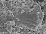
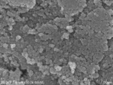
- Example 1 It is an electron micrograph which shows the copper powder used in Example 1 (magnification 5,000 times). It is an electron micrograph which shows the silver fine particle used in Example 1 (magnification 5,000 times). It is an electron micrograph which shows the silver fine particle used in Example 1 (magnification 50,000 times). It is an electron micrograph which shows the silver hybrid copper powder obtained in Example 1 (magnification 5,000 times).
- the silver fine particle powder adheres to the surface of the copper powder, and the ratio (D SEM ) of the average particle diameter (D 50 ) of the copper powder and the average particle diameter (D SEM ) of the silver fine particles 50 / D SEM ) is in the range of 3 to 400, and the ratio of the tap density of the copper powder to the silver fine particles is in the range of 0.5 to 1.5.
- the average particle diameter (D 50 ) according to the laser diffraction / scattering particle size distribution of the silver hybrid copper powder according to the present invention is preferably 0.1 to 50 ⁇ m, more preferably 0.1 to 40 ⁇ m, still more preferably 0.1. ⁇ 30 ⁇ m. It may also be used in combination with different silver hybrid copper powder of an average particle diameter (D 50).
- the average particle size (D 50 ) is less than 0.1 ⁇ m, surface oxidation is likely to occur due to particle miniaturization, and conductivity is lowered, which is not preferable.
- the average particle diameter (D 50) is more than 50 ⁇ m, since the printing property and filling property of the resulting conductive paste decreases by using this, is possible to obtain a conductive paste having high conductivity It becomes difficult.
- the particle shape of the silver hybrid copper powder according to the present invention is not particularly limited, and may be a spherical shape, a dendritic shape, a flake shape, a needle shape, a plate shape, a granular shape, or the like. Moreover, you may use combining silver hybrid copper powder from which a shape differs.
- the tap density of the silver hybrid copper powder according to the present invention is preferably 2.0 g / cm 3 or more, more preferably 2.5 g / cm 3 or more, still more preferably 3.0 g / cm 3 or more, even more. Preferably it is 3.5 g / cm 3 or more.
- the tap density is less than 2.0 g / cm 3, it is difficult to increase the filling rate of the silver hybrid copper powder in the fine wiring formed by the conductive paste containing the silver hybrid copper powder, and the electric resistance value is reduced. Is disadvantageous.
- the BET specific surface area value of the silver hybrid copper powder according to the present invention is preferably 4.0 m 2 / g or less, more preferably 0.1 to 3.0 m 2 / g.
- the BET specific surface area value exceeds 4.0 m 2 / g, the surface area of the particle powder is too large, so that surface oxidation is liable to occur and conductivity is lowered, which is not preferable.
- the ratio (D 50 / D SEM ) of the average particle diameter (D 50 ) of the copper powder and the average particle diameter (D SEM ) of the silver fine particle powder is in the range of 3 to 400. , Preferably 4 to 350, more preferably 5 to 300.
- the ratio of the average particle size of the copper powder and the (D 50) and the average particle diameter of the silver fine powder (D SEM) in the case of less than (D 50 / D SEM) is 3, the average particle diameter (D 50) of copper powder
- the average particle diameter (D SEM ) of the silver fine particle powder is too large, it is difficult to coat the silver fine particle powder on the particle surface of the copper powder, and it is difficult to obtain a conductive paste having high conductivity. It becomes.
- the ratio of the tap density of the copper powder and the silver fine particle powder is in the range of 0.5 to 1.5, preferably 0.55 to 1.45, more preferably 0.6. It is in the range of ⁇ 1.4.
- the ratio of the tap density of the copper powder and the silver fine particle powder is in the above range, that is, when the tap density value of the copper powder and the silver fine particle powder is close, the surface of the copper powder particle is coated with the silver fine particle powder. Since the copper powder and the silver fine particle powder behave together without being separated, a more effective coating treatment with the silver fine particle powder can be performed.
- the proportion of silver fine particles adhering to the silver hybrid copper powder according to the present invention depends on the BET specific surface area value of the copper powder, but the silver fine particles are 1 to 300 parts by weight with respect to 100 parts by weight of the copper powder. More preferred is 2 to 200 parts by weight, still more preferred is 3 to 150 parts by weight.
- the coating amount with the silver fine particles is less than 1 part by weight, the adhesion amount of the silver fine particles is too small, so that a sufficient conductivity improving effect by coating the silver fine particles cannot be obtained.
- the exposed surface of the copper powder which is a core material increases, and copper powder is oxidized and it becomes difficult to ensure sufficient electroconductivity.
- the upper limit is 300 parts by weight in consideration of the balance between the effect of improving oxidation resistance and conductivity and the cost of the obtained silver hybrid copper powder. Further, since the abundance of silver fine particles on the particle surface is increased, a silver migration phenomenon tends to occur, which is not preferable.
- the particle surface of the copper powder is uniformly coated with silver fine particles, and a part of the copper powder may be exposed depending on the purpose.
- the silver hybrid copper powder according to the present invention can be obtained by mixing and stirring the copper powder and the silver fine particle powder and attaching the silver fine particle powder to the particle surface of the copper powder.
- the copper powder in the present invention is not limited in its type, production method, and the like, and copper powder obtained from a normal electrolysis method, reduction method, atomization method, mechanical grinding, or the like can be used.
- the particle shape of the copper powder in the present invention is not particularly limited, and a spherical shape, a dendritic shape, a scale shape, a flake shape, a needle shape, a plate shape, a granular shape, and the like can be used. Moreover, you may use combining the copper powder from which a shape differs.
- the average particle diameter (D 50 ) of the copper powder according to the laser diffraction / scattering particle size distribution is preferably 0.1 to 50 ⁇ m, more preferably 0.1 to 40 ⁇ m, still more preferably 0.1 to 30 ⁇ m. is there. It may be used in combination with different copper powder of an average particle diameter (D 50).
- the average particle size (D 50 ) is less than 0.1 ⁇ m, surface oxidation is likely to occur due to particle miniaturization, and conductivity is lowered, which is not preferable.
- the average particle diameter (D 50) is more than 50 ⁇ m, the reduced printability and filling of the obtained conductive paste using silver hybrid copper powder and silver hybrid copper powder obtained by using the Therefore, it is difficult to obtain a conductive paste having high conductivity.
- the tap density of the copper powder in the present invention is preferably 1.5 g / cm 3 or more, more preferably 2.0 g / cm 3 or more, and even more preferably 2.5 g / cm 3 or more. If the tap density is less than 1.5 g / cm 3, a tap density of the silver hybrid copper powder obtained it becomes difficult to 2.0 g / cm 3 or more.
- the BET specific surface area value of the copper powder in the present invention is preferably 4.0 m 2 / g or less, more preferably 0.05 to 3.0 m 2 / g.
- the BET specific surface area value exceeds 4.0 m 2 / g, the surface area of the particle powder is too large, so that surface oxidation is liable to occur and conductivity is lowered, which is not preferable.
- the silver fine particle powder in the present invention is not limited in its type, production method and the like, and silver fine particles obtained by a known method such as a normal mechanical pulverization method, an atomization method, a wet reduction method, an electrolysis method, a gas phase method, etc. Powder can be used.
- the particle shape of the silver fine particles in the present invention is not particularly limited, and may be spherical, granular, amorphous, dendritic, flake-like, plate-like, needle-like, etc., but may be spherical, granular or irregular. preferable.
- the average particle diameter (D SEM ) of the silver fine particle powder in the present invention is preferably 30 to 300 nm, more preferably 35 to 200 nm, and more preferably 40 to 100 nm.
- D SEM average particle diameter
- the tap density of the silver fine particle powder in the present invention is 3.0 g / cm 3 or more, preferably 3.2 g / cm 3 or more, more preferably 3.4 g / cm 3 or more.
- the upper limit of the tap density of the silver fine particles is about 6.0 g / cm 3 , and more preferably about 5.5 g / cm 3 .
- an apparatus capable of applying mechanical energy to the powder layer is preferable.
- a ball-type kneader or a wheel-type kneader can be used. It can be used more effectively.
- the ball-type kneader includes a vibration mill, a rotary mill, a sand grinder, and preferably a vibration mill.
- the wheel-type kneader include edge runners (synonymous with “mix muller”, “Simpson mill”, “sand mill”), multi-mal, stotz mill, wet pan mill, conner mill, ring muller, and the like.
- the mixing and stirring of the copper powder and the silver fine particle powder is preferably performed in an N 2 atmosphere in order to prevent all the steps from being dry and to prevent a decrease in conductivity due to oxidation of the copper powder.
- the conductive paste according to the present invention is composed of the silver hybrid copper powder according to the present invention and a solvent, and may contain other components such as a binder resin, a curing agent, a dispersant, and a rheology modifier as necessary. .
- arbitrary conductive fillers such as metal powders, such as platinum, gold
- binder resin those known in the art can be used, for example, cellulose resins such as methyl cellulose, ethyl cellulose, hydroxyethyl cellulose, nitrocellulose, ethyl cellulose derivatives, polyester resins, urethane-modified polyester resins, epoxy-modified polyester resins.
- Various modified polyester resins such as acrylic modified polyester, polyurethane resin, vinyl chloride / vinyl acetate copolymer, acrylic resin, epoxy resin, phenolic resin, melamine resin, alkyd resin, butyral resin, polyvinyl alcohol, polyimide resin, Examples thereof include inorganic binders such as polyamideimide resin, amino resin, styrene resin, resol resin, and glass frit. These binder resins can be used alone or in combination of two or more.
- solvent those known in the art can be used, and examples thereof include tetradecane, toluene, xylene, ethylbenzene, diethylbenzene, isopropylbenzene, amylbenzene, p-cymene, tetralin, and petroleum aromatic hydrocarbon mixtures.
- Hydrocarbon solvents ethylene glycol monoethyl ether, ethylene glycol monobutyl ether, propylene glycol monomethyl ether, propylene glycol monoethyl ether, propylene glycol mono-n-butyl ether, propylene glycol mono-t-butyl ether, diethylene glycol monoethyl ether, diethylene glycol Monobutyl ether, dipropylene glycol monomethyl ether, dipropylene glycol monobutyl ether, Ether or glycol ether solvents such as propylene glycol monomethyl ether; glycol ester solvents such as ethylene glycol monomethyl ether acetate, ethylene glycol monoethyl ether acetate, ethylene glycol monobutyl ether acetate, propylene glycol monomethyl ether acetate, propylene glycol monoethyl ether acetate Ester solvents such as ethyl acetate and butyl acetate; ketone solvents such as
- the content of the silver hybrid copper powder in the conductive paste varies depending on the application. For example, in the case of wiring formation, it is preferably as close to 100% by weight as possible.
- the conductive paste according to the present invention is obtained by mixing and dispersing each component using various kneaders and dispersers such as a laika machine, a pot mill, a three roll mill, a rotary mixer, a twin screw mixer, and the like. Can do.
- the conductive paste according to the present invention is applied to various coating methods such as screen printing, intaglio printing, flat plate printing, inkjet method, gravure printing, transfer printing, roll coating, flow coating, spray coating, spin coating, dipping, blade coating, plating, etc. Applicable.
- the conductive paste according to the present invention is used for forming electrodes such as FPD (flat panel display), solar cell, organic EL, wiring for LSI substrates, and wiring for filling fine trenches, via holes, contact holes, etc. It can be used as a material.
- FPD flat panel display
- organic EL organic EL
- wiring for LSI substrates and wiring for filling fine trenches, via holes, contact holes, etc.
- It can be used as a material.
- FPD flat panel display
- organic EL organic EL
- An important point in the present invention is the fact that the silver hybrid copper powder obtained using copper powder and silver fine particles having a specific average particle diameter and tap density is excellent in conductivity and migration resistance.
- the silver hybrid copper powder according to the present invention is excellent in conductivity as follows. That is, the silver hybrid copper powder of the present invention is treated in an aqueous solution such as a method of coating silver on the surface of copper particles by a known substitution reaction between silver ions and metallic copper, or a silver plating method. By not carrying out the process, it is possible to prevent a decrease in conductivity due to oxidation of the copper powder in the aqueous solution, and thus it is considered that excellent conductivity could be obtained even with a small amount of silver fine particles. In addition, by using a copper powder and silver fine particles that are close to each other, it is possible to perform coating treatment with better adhesion of silver fine particles to the copper particle surface without uneven distribution of copper powder and silver fine particles. I think it was because
- the present inventor considers the reason why the silver hybrid copper powder according to the present invention is excellent in migration resistance as follows. That is, when the particle surface is covered with silver as in the plating process, a migration phenomenon is likely to occur, but the silver hybrid copper powder of the present invention does not uniformly cover the particle surface of the copper particle with silver fine particles. It is considered that the occurrence of the migration phenomenon could be suppressed because excellent conductivity was obtained.
- the average particle size (D SEM ) of the silver fine particles was obtained by taking a photograph of the particles using a scanning electron micrograph “S-4800” (manufactured by HITACHI) and measuring the particle size of 100 or more particles using the photograph. And the average value was computed and it was set as the average particle diameter ( DSEM ).
- the average particle diameter (D 50 ) of the copper powder and the silver hybrid copper powder was measured using a laser diffraction / scattering particle size distribution measuring device “LMS-2000e” (manufactured by Seishin Enterprise Co., Ltd.). The particle diameter is shown as 50%.
- the specific surface area values of copper powder, silver fine particles and silver hybrid copper powder were shown as values measured by the BET method using “Monosorb MS-11” (manufactured by Kantachrome Co., Ltd.).
- the content of copper and silver constituting the silver hybrid copper powder is as follows: 0.2 g of sample, 5 ml of nitric acid and 10 ml of ion exchange water are placed in a 50 ml fluororesin beaker and kept at 240 ° C. for 15 minutes to dissolve. Was measured using an “inductively coupled plasma optical emission spectrometer iCAP6500Duo” (manufactured by Thermo Fisher Scientific Co., Ltd.).
- the specific resistance of the conductive coating film is obtained by applying a conductive paste described later on a polyimide film having a thickness of 50 ⁇ m, preliminarily drying at 120 ° C. for 10 minutes, and then heating at 240 ° C. for 5 minutes in an N 2 atmosphere.
- the conductive film was measured using a four-terminal electric resistance measuring device “Loresta GP / MCP-T610” (manufactured by Dia Instruments Co., Ltd.), and the specific resistance was calculated from the sheet resistance and the film thickness.
- the migration resistance of the conductive coating film is obtained by forming a pattern with a line width of 0.75 mm and a length of 25.0 mm with a gap of 0.75 mm in the center using a conductive paste described later on a polyimide film having a thickness of 50 ⁇ m.
- a sample was screen-printed so as to have a dry film thickness of 10 to 30 ⁇ m, and dried by heating at 150 ° C. for 30 minutes.
- Example 1-1 Production of silver hybrid copper powder> Copper powder 1 (shape: dendritic, average particle diameter D 50 : 10.5 ⁇ m, BET specific surface area value: 0.3 m 2 / g, tap density: 3.4 g / cm 3 ) 1.8 kg of vibration mill “MB1” (Media: ⁇ 11 m / m resin-coated sphere 3.9 kg) (Product name, manufactured by Chuo Kako Co., Ltd.), then silver fine particles 1 (shape: irregular, average particle diameter D SEM : 75 nm, BET ratio 200 g of surface area value: 3.1 m 2 / g, tap density: 4.6 g / cm 3 ) was added, and the mixture was stirred for 180 minutes at a rotation speed of 1200 rpm and an amplitude of 6 mm to obtain the silver hybrid copper powder of Example 1-1. Obtained.
- Copper powder 1 shape: dendritic, average particle diameter D 50 : 10.5 ⁇ m, BET specific surface area value:
- the obtained silver hybrid copper powder has a dendritic particle shape, an average particle diameter (D 50 ) of 6.7 ⁇ m, a BET specific surface area value of 0.47 m 2 / g, a tap density of 4.40 g / cm 3 ,
- the Ag content was 9.11% and the Cu content was 90.89%.
- the ratio (D 50 / D SEM ) of the average particle size (D 50 ) of the copper powder and the average particle size (D SEM ) of the silver fine particle powder is 140.0, and the ratio of the tap density of the copper powder and the silver fine particle powder was 0.74.
- FIG. 1 shows an electron micrograph of the copper powder used in Example 1, and FIG. 2 (magnification 5,000 times) and FIG. 3 (magnification 50,000 times) show the obtained silver microparticles.
- An electron micrograph of the hybrid copper powder is shown in FIG.
- FIG. 4 As a result of observing an electron micrograph, although silver fine particles are not observed in FIG. 4, it is recognized that a predetermined amount of silver is detected when the silver content is measured, so that the silver fine particles are complexed with copper powder. It was.
- Example 2-1 Production of conductive paste> A silver hybrid in a conductive paste was prepared by adding a polyester resin diethylene glycol monobutyl ether acetate solution (solid content 35%) and diethylene glycol monobutyl ether acetate and diethylene glycol monoethyl ether acetate to 100 parts by weight of the silver hybrid copper powder of Example 1-1. After adjusting so that content of copper powder might be 88 wt% (91 wt% as solid content), it premixed and knead
- the obtained conductive paste was applied on a polyimide film having a thickness of 50 ⁇ m, and was dried by heating at 240 ° C. for 5 minutes in a nitrogen atmosphere for measuring specific resistance, and heated at 150 ° C. for 10 minutes in a nitrogen atmosphere for measuring migration resistance. It dried and obtained the electroconductive coating film.
- the specific resistance value of the obtained conductive coating film was 4.7 ⁇ 10 ⁇ 2 ⁇ ⁇ cm, and the migration resistance was 588 sec.
- Silver hybrid copper powder and conductive paste were prepared according to Example 1-1 and Example 2-1. Various characteristics of each production condition and the obtained silver hybrid copper powder and electric paste are shown.
- Copper powder 1-5 Copper powder having the characteristics shown in Table 1 was prepared as copper powder.
- Silver fine particles 1-7 Silver fine particle powder having the characteristics shown in Table 2 was prepared as silver fine particles.
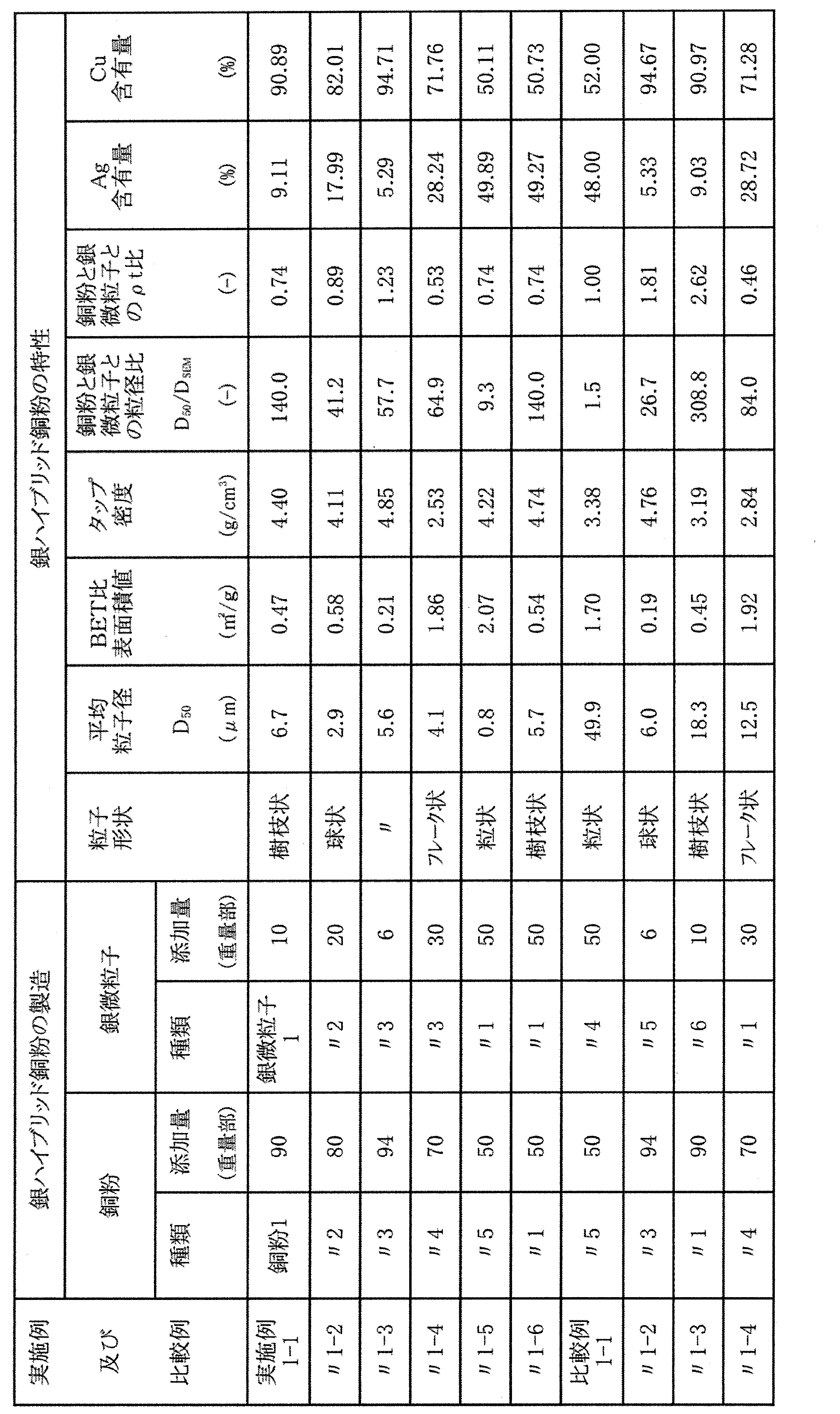
- Examples 1-2 to 1-6 and Comparative Examples 1-1 to 1-4 A silver hybrid copper powder was obtained in the same manner as in Example 1-1 except that the type of copper powder, the type of silver fine particles, and the amount added were changed.
- Table 3 shows the manufacturing conditions and various characteristics of the silver hybrid copper powder.
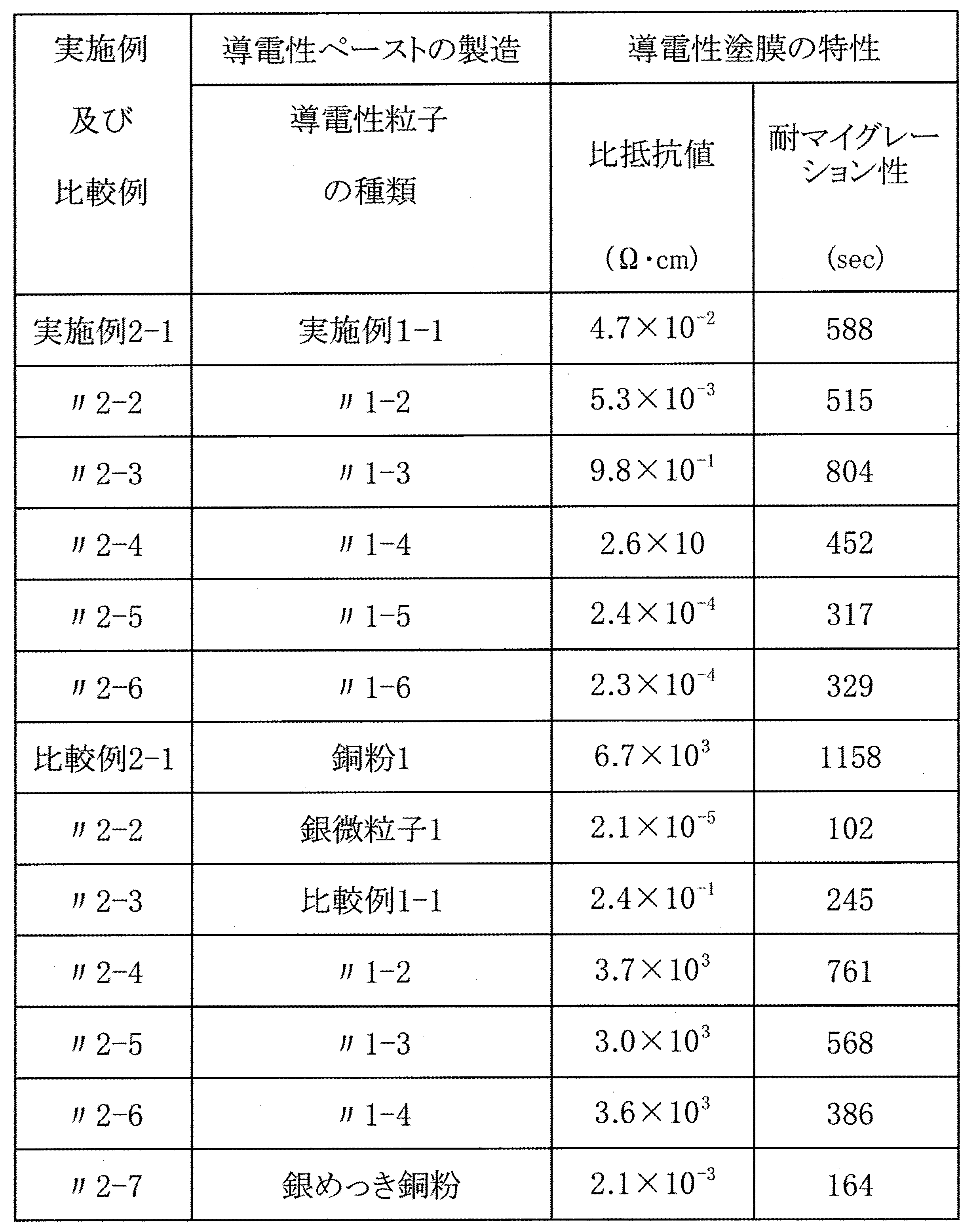
- Examples 2-2 to 2-6 and comparative examples 2-1 to 2-7 A conductive paste and a conductive coating film were produced according to the method for producing a conductive paste of Example 2-1 except that the type of the silver hybrid copper powder was variously changed.
- the conductive particles of Comparative Example 2-7 were commercially available silver-plated copper powder (particle shape: dendritic, average particle diameter (D 50 ): 10.7 ⁇ m, BET specific surface area value: 0.43 m 2 / g, tap. Density: 2.99 g / cm 3 , Ag content: 9.60%, Cu content: 90.34%).
- Table 4 shows the manufacturing conditions and various characteristics of the obtained conductive coating film.
- the silver hybrid copper powder according to the present invention is excellent in conductivity, conductivity and migration resistance, it is suitable as a raw material for conductive paste, conductive adhesive and the like.
- the conductive paste and the conductive adhesive using the silver hybrid copper powder according to the present invention can provide a printed wiring board and the like excellent in migration resistance and conductivity, the conductivity used in various electronic devices. Suitable as paste and conductive adhesive.
Landscapes
- Chemical & Material Sciences (AREA)
- Engineering & Computer Science (AREA)
- Nanotechnology (AREA)
- Inorganic Chemistry (AREA)
- Dispersion Chemistry (AREA)
- Organic Chemistry (AREA)
- Physics & Mathematics (AREA)
- Microelectronics & Electronic Packaging (AREA)
- Spectroscopy & Molecular Physics (AREA)
- General Physics & Mathematics (AREA)
- Materials Engineering (AREA)
- Crystallography & Structural Chemistry (AREA)
- Condensed Matter Physics & Semiconductors (AREA)
- Composite Materials (AREA)
- Powder Metallurgy (AREA)
- Conductive Materials (AREA)
- Manufacturing & Machinery (AREA)
- Non-Insulated Conductors (AREA)
Description
本発明において重要な点は、特定の平均粒子径とタップ密度を有する銅粉と銀微粒子を用いて得られた銀ハイブリッド銅粉は、導電性及び耐マイグレーション性に優れているという事実である。
銅粉1(形状:樹枝状、平均粒子径D50:10.5μm、BET比表面積値:0.3m2/g、タップ密度:3.4g/cm3)1.8kgを振動ミル「MB1」(メディア:φ11m/mの樹脂コート球 3.9kg)(製品名、中央化工機株式会社製)に投入し、次いで、銀微粒子1(形状:不定形、平均粒子径DSEM:75nm、BET比表面積値:3.1m2/g、タップ密度:4.6g/cm3)200gを添加し、回転数1200rpm、振幅6mmで180分間混合攪拌を行い、実施例1-1の銀ハイブリッド銅粉を得た。
実施例1-1の銀ハイブリッド銅粉100重量部に対してポリエステル樹脂のジエチレングリコールモノブチルエーテルアセテート溶液(固形分35%)およびジエチレングリコールモノブチルエーテルアセテートとジエチレングリコールモノエチルエーテルアセテートを加え、導電性ペーストにおける銀ハイブリッド銅粉の含有量が88wt%(固形分として91wt%)となるよう調整した後、プレミックスを行い、3本ロールを用いて均一に混練・分散処理を行った。次いで、導電性ペーストにおける固形分が70wt%となるようにジエチレングリコールモノブチルエーテルアセテートとジエチレングリコールモノエチルエーテルアセテートの混合溶液を加え、分散・混合処理を行って、実施例2-1の導電性ペーストを得た。
銅粉として表1に示す特性を有する銅粉を用意した。

銀微粒子として表2に示す特性を有する銀微粒子粉末を用意した。

銅粉の種類、銀微粒子の種類及び添加量を変化させた以外は、前記実施例1-1と同様にして銀ハイブリッド銅粉を得た。
銀ハイブリッド銅粉の種類を種々変化させた以外は、前記実施例2-1の導電性ペーストの作製方法に従って導電性ペースト及び導電性塗膜を製造した。なお、比較例2-7の導電性粒子は市販の銀メッキ銅粉(粒子形状:樹枝状、平均粒子径(D50):10.7μm、BET比表面積値:0.43m2/g、タップ密度:2.99g/cm3、Ag含有量:9.60%、Cu含有量:90.34%)である。
Claims (10)
- 銅粉の表面に銀微粒子粉末が付着しており、銅粉の平均粒子径(D50)と銀微粒子の平均粒子径(DSEM)との比(D50/DSEM)が3~400の範囲であり、且つ、銅粉と銀微粒子のタップ密度の比が0.5~1.5の範囲にあることを特徴とする銀ハイブリッド銅粉。
- タップ密度が2.0g/cm3以上である請求項1記載の銀ハイブリッド銅粉。
- レーザー回折散乱粒度分布による平均粒子径(D50)が0.1~50μmである請求項1又は2記載の銀ハイブリッド銅粉。
- 銅粉100重量部に対して銀微粒子の付着量が1~300重量部である請求項1~3のいずれかに記載の銀ハイブリッド銅粉。
- 銀微粒子の平均粒子径(DSEM)が30~300nmであり、タップ密度が3.0g/cm3以上である請求項1~4のいずれかに記載の銀ハイブリッド銅粉。
- 銅粉末と銀微粒子粉末とを混合攪拌して銅粉末の粒子表面に銀微粒子粉末を付着させる銀ハイブリッド銅粉の製造法において、全処理工程を乾式で行うと共に、銅粉の平均粒子径(D50)と銀微粒子の平均粒子径(DSEM)との比(D50/DSEM)が3~400の範囲であり、且つ、銅粉と銀微粒子のタップ密度の比が0.5~1.5の範囲にある銅粉と銀微粒子粉末を用いることを特徴とする請求項1~5のいずれかに記載の銀ハイブリッド銅粉の製造法。
- 請求項1~5のいずれかに記載の銀ハイブリッド銅粉を含む導電性接着剤。
- 請求項1~5のいずれかに記載の銀ハイブリッド銅粉を含む導電性ペースト。
- 請求項8記載の導電性ペーストを用いて形成された導電性膜。
- 請求項8記載の導電性ペーストを用いて形成された電気回路。
Priority Applications (3)
| Application Number | Priority Date | Filing Date | Title |
|---|---|---|---|
| KR1020157008332A KR20150064054A (ko) | 2012-10-03 | 2013-10-01 | 은 하이브리드 구리분과 그의 제조법, 상기 은 하이브리드 구리분을 함유하는 도전성 페이스트, 도전성 접착제, 도전성 막 및 전기 회로 |
| CN201380060057.4A CN104797360A (zh) | 2012-10-03 | 2013-10-01 | 银混合铜粉及其制造方法、含有该银混合铜粉的导电性膏、导电性粘合剂、导电性膜和电气回路 |
| JP2014539750A JPWO2014054618A1 (ja) | 2012-10-03 | 2013-10-01 | 銀ハイブリッド銅粉とその製造法、該銀ハイブリッド銅粉を含有する導電性ペースト、導電性接着剤、導電性膜、及び電気回路 |
Applications Claiming Priority (2)
| Application Number | Priority Date | Filing Date | Title |
|---|---|---|---|
| JP2012-221321 | 2012-10-03 | ||
| JP2012221321 | 2012-10-03 |
Publications (1)
| Publication Number | Publication Date |
|---|---|
| WO2014054618A1 true WO2014054618A1 (ja) | 2014-04-10 |
Family
ID=50434944
Family Applications (1)
| Application Number | Title | Priority Date | Filing Date |
|---|---|---|---|
| PCT/JP2013/076664 Ceased WO2014054618A1 (ja) | 2012-10-03 | 2013-10-01 | 銀ハイブリッド銅粉とその製造法、該銀ハイブリッド銅粉を含有する導電性ペースト、導電性接着剤、導電性膜、及び電気回路 |
Country Status (5)
| Country | Link |
|---|---|
| JP (1) | JPWO2014054618A1 (ja) |
| KR (1) | KR20150064054A (ja) |
| CN (1) | CN104797360A (ja) |
| TW (1) | TW201424887A (ja) |
| WO (1) | WO2014054618A1 (ja) |
Cited By (2)
| Publication number | Priority date | Publication date | Assignee | Title |
|---|---|---|---|---|
| JPWO2017188123A1 (ja) * | 2016-04-28 | 2019-03-07 | 日立化成株式会社 | 接合用銅ペースト、接合体の製造方法及び半導体装置の製造方法 |
| WO2019181650A1 (ja) * | 2018-03-19 | 2019-09-26 | 日本電産株式会社 | 電気接点用粉末、電気接点材料、電気接点及び電気接点用粉末の製造方法 |
Families Citing this family (7)
| Publication number | Priority date | Publication date | Assignee | Title |
|---|---|---|---|---|
| JP6811080B2 (ja) * | 2016-02-03 | 2021-01-13 | Dowaエレクトロニクス株式会社 | 銀被覆銅粉およびその製造方法 |
| CN108026420B (zh) * | 2016-05-12 | 2020-11-06 | 日本Mektron株式会社 | 导电性粘合剂和屏蔽膜 |
| TWI617533B (zh) | 2016-12-09 | 2018-03-11 | 財團法人工業技術研究院 | 表面改質陶瓷粉體及其應用 |
| CN109892020B (zh) * | 2017-02-13 | 2022-03-04 | 拓自达电线株式会社 | 接地构件、屏蔽印制线路板及屏蔽印制线路板的制造方法 |
| KR102521531B1 (ko) | 2017-08-31 | 2023-04-14 | 한국광기술원 | 금속환원성 유기물로 코팅된 은 및 구리 나노입자를 포함하는 전자소자 접착용 조성물 및 이의 제조방법, 이를 적용한 전자기기 |
| WO2020137329A1 (ja) * | 2018-12-26 | 2020-07-02 | 昭栄化学工業株式会社 | 銀ペースト |
| TWI884347B (zh) * | 2021-03-26 | 2025-05-21 | 日商拓自達電線股份有限公司 | 導電性接著劑層 |
Citations (3)
| Publication number | Priority date | Publication date | Assignee | Title |
|---|---|---|---|---|
| JPH04218602A (ja) * | 1990-12-18 | 1992-08-10 | Fukuda Metal Foil & Powder Co Ltd | 金属被覆複合粉末の製造方法 |
| JP2005015910A (ja) * | 2003-06-03 | 2005-01-20 | Hosokawa Funtai Gijutsu Kenkyusho:Kk | 複合粒子の製造方法、並びにその方法により製造された複合粒子 |
| JP2007100155A (ja) * | 2005-10-03 | 2007-04-19 | Mitsui Mining & Smelting Co Ltd | 微粒銀粒子付着銀銅複合粉及びその微粒銀粒子付着銀銅複合粉製造方法 |
Family Cites Families (5)
| Publication number | Priority date | Publication date | Assignee | Title |
|---|---|---|---|---|
| JP4779134B2 (ja) * | 2001-02-13 | 2011-09-28 | Dowaエレクトロニクス株式会社 | 導電ペースト用の導電フイラーおよびその製法 |
| DE102004032903B4 (de) * | 2003-07-08 | 2006-06-29 | Hitachi Chemical Co., Ltd. | Leitfähiges Pulver und Verfahren zur Herstellung desselben |
| EP1752994A4 (en) * | 2004-06-17 | 2007-11-28 | Matsushita Electric Industrial Co Ltd | PROCESS FOR MANUFACTURING A SELF-ASSEMBLED RARE-IRON BOND MAGNET AND MOTOR THEREWITH |
| JPWO2008059789A1 (ja) * | 2006-11-17 | 2010-03-04 | 日鉱金属株式会社 | 銀メッキ銅微粉及び銀メッキ銅微粉を用いて製造した導電ペースト並びに銀メッキ銅微粉の製造方法 |
| JP2010065265A (ja) * | 2008-09-10 | 2010-03-25 | Hitachi Ltd | 金属ナノ粒子及びその複合粉末の作製方法 |
-
2013
- 2013-10-01 KR KR1020157008332A patent/KR20150064054A/ko not_active Withdrawn
- 2013-10-01 JP JP2014539750A patent/JPWO2014054618A1/ja active Pending
- 2013-10-01 WO PCT/JP2013/076664 patent/WO2014054618A1/ja not_active Ceased
- 2013-10-01 CN CN201380060057.4A patent/CN104797360A/zh active Pending
- 2013-10-03 TW TW102135830A patent/TW201424887A/zh unknown
Patent Citations (3)
| Publication number | Priority date | Publication date | Assignee | Title |
|---|---|---|---|---|
| JPH04218602A (ja) * | 1990-12-18 | 1992-08-10 | Fukuda Metal Foil & Powder Co Ltd | 金属被覆複合粉末の製造方法 |
| JP2005015910A (ja) * | 2003-06-03 | 2005-01-20 | Hosokawa Funtai Gijutsu Kenkyusho:Kk | 複合粒子の製造方法、並びにその方法により製造された複合粒子 |
| JP2007100155A (ja) * | 2005-10-03 | 2007-04-19 | Mitsui Mining & Smelting Co Ltd | 微粒銀粒子付着銀銅複合粉及びその微粒銀粒子付着銀銅複合粉製造方法 |
Cited By (2)
| Publication number | Priority date | Publication date | Assignee | Title |
|---|---|---|---|---|
| JPWO2017188123A1 (ja) * | 2016-04-28 | 2019-03-07 | 日立化成株式会社 | 接合用銅ペースト、接合体の製造方法及び半導体装置の製造方法 |
| WO2019181650A1 (ja) * | 2018-03-19 | 2019-09-26 | 日本電産株式会社 | 電気接点用粉末、電気接点材料、電気接点及び電気接点用粉末の製造方法 |
Also Published As
| Publication number | Publication date |
|---|---|
| CN104797360A (zh) | 2015-07-22 |
| KR20150064054A (ko) | 2015-06-10 |
| JPWO2014054618A1 (ja) | 2016-08-25 |
| TW201424887A (zh) | 2014-07-01 |
Similar Documents
| Publication | Publication Date | Title |
|---|---|---|
| WO2014054618A1 (ja) | 銀ハイブリッド銅粉とその製造法、該銀ハイブリッド銅粉を含有する導電性ペースト、導電性接着剤、導電性膜、及び電気回路 | |
| JP2012214898A (ja) | 銀コート銅粉及びその製造法、該銀コート銅粉を含有する導電性ペースト、導電性接着剤、導電性膜、及び電気回路 | |
| JP4363340B2 (ja) | 導電性銀ペースト及びそれを用いた電磁波シールド部材 | |
| TWI490063B (zh) | Silver fine particles and a method for producing the same, and an electric paste containing the silver fine particles, a conductive film, and an electronic device | |
| JP5937730B2 (ja) | 銅粉の製造方法 | |
| CN108140443B (zh) | 导电浆料和导电膜 | |
| TWI622998B (zh) | 導電性組成物及使用其之硬化物 | |
| CN101836268B (zh) | 铜配线图案形成方法以及用于其中的氧化铜粒子分散液 | |
| CN1671805A (zh) | 烧结温度低的导电纳米油墨及其制备方法 | |
| CN103013229A (zh) | 一种石墨烯基导电油墨、其制备方法及柔性导电薄膜 | |
| JP2006049147A (ja) | 導電性ペースト | |
| CN102737749A (zh) | 导电粒子、导电胶以及电路板 | |
| JP2017527943A (ja) | 導電性組成物 | |
| CN103624987A (zh) | 聚合物厚膜导体组合物的光子烧结 | |
| JP2013028859A (ja) | 銀微粒子並びに該銀微粒子を含有する導電性ペースト、導電性膜及び電子デバイス | |
| CN103219062A (zh) | 聚合物厚膜焊料合金导体组合物 | |
| JP6681437B2 (ja) | 導電性ペースト | |
| JP2012031478A (ja) | 銀微粒子とその製造方法、並びに該銀微粒子を含有する導電性ペースト、導電性膜及び電子デバイス | |
| WO2019009146A1 (ja) | 導電性ペースト | |
| JP4881013B2 (ja) | 導電性粉末、導電性ペーストおよび電気回路 | |
| JP7563007B2 (ja) | 導体形成用銅ペースト、導体膜を有する物品及びそれらの製造方法 | |
| CN103722864B (zh) | 用于电子装置中的聚合物厚膜导体组合物 | |
| CN110698925A (zh) | 一种纳米印刷导电油墨组合物及其制备方法和应用 | |
| JP2016138300A (ja) | 銅粉、及びそれを用いた銅ペースト、導電性塗料、導電性シート | |
| JP2000328232A (ja) | 導電性粉末およびその製造方法並びにそれを使用した塗料 |
Legal Events
| Date | Code | Title | Description |
|---|---|---|---|
| 121 | Ep: the epo has been informed by wipo that ep was designated in this application |
Ref document number: 13844362 Country of ref document: EP Kind code of ref document: A1 |
|
| ENP | Entry into the national phase |
Ref document number: 2014539750 Country of ref document: JP Kind code of ref document: A |
|
| ENP | Entry into the national phase |
Ref document number: 20157008332 Country of ref document: KR Kind code of ref document: A |
|
| NENP | Non-entry into the national phase |
Ref country code: DE |
|
| 122 | Ep: pct application non-entry in european phase |
Ref document number: 13844362 Country of ref document: EP Kind code of ref document: A1 |