WO2014050408A1 - 光学補償板 - Google Patents
光学補償板 Download PDFInfo
- Publication number
- WO2014050408A1 WO2014050408A1 PCT/JP2013/072855 JP2013072855W WO2014050408A1 WO 2014050408 A1 WO2014050408 A1 WO 2014050408A1 JP 2013072855 W JP2013072855 W JP 2013072855W WO 2014050408 A1 WO2014050408 A1 WO 2014050408A1
- Authority
- WO
- WIPO (PCT)
- Prior art keywords
- layer
- optical
- antireflection
- antireflection layer
- compensation
- Prior art date
- Legal status (The legal status is an assumption and is not a legal conclusion. Google has not performed a legal analysis and makes no representation as to the accuracy of the status listed.)
- Ceased
Links
Images



Classifications
-
- G—PHYSICS
- G02—OPTICS
- G02B—OPTICAL ELEMENTS, SYSTEMS OR APPARATUS
- G02B1/00—Optical elements characterised by the material of which they are made; Optical coatings for optical elements
- G02B1/10—Optical coatings produced by application to, or surface treatment of, optical elements
- G02B1/11—Anti-reflection coatings
-
- G—PHYSICS
- G02—OPTICS
- G02B—OPTICAL ELEMENTS, SYSTEMS OR APPARATUS
- G02B1/00—Optical elements characterised by the material of which they are made; Optical coatings for optical elements
- G02B1/10—Optical coatings produced by application to, or surface treatment of, optical elements
- G02B1/11—Anti-reflection coatings
- G02B1/118—Anti-reflection coatings having sub-optical wavelength surface structures designed to provide an enhanced transmittance, e.g. moth-eye structures
-
- G—PHYSICS
- G02—OPTICS
- G02B—OPTICAL ELEMENTS, SYSTEMS OR APPARATUS
- G02B1/00—Optical elements characterised by the material of which they are made; Optical coatings for optical elements
- G02B1/10—Optical coatings produced by application to, or surface treatment of, optical elements
- G02B1/18—Coatings for keeping optical surfaces clean, e.g. hydrophobic or photo-catalytic films
-
- G—PHYSICS
- G02—OPTICS
- G02B—OPTICAL ELEMENTS, SYSTEMS OR APPARATUS
- G02B5/00—Optical elements other than lenses
- G02B5/30—Polarising elements
- G02B5/3083—Birefringent or phase retarding elements
-
- G—PHYSICS
- G02—OPTICS
- G02F—OPTICAL DEVICES OR ARRANGEMENTS FOR THE CONTROL OF LIGHT BY MODIFICATION OF THE OPTICAL PROPERTIES OF THE MEDIA OF THE ELEMENTS INVOLVED THEREIN; NON-LINEAR OPTICS; FREQUENCY-CHANGING OF LIGHT; OPTICAL LOGIC ELEMENTS; OPTICAL ANALOGUE/DIGITAL CONVERTERS
- G02F1/00—Devices or arrangements for the control of the intensity, colour, phase, polarisation or direction of light arriving from an independent light source, e.g. switching, gating or modulating; Non-linear optics
- G02F1/01—Devices or arrangements for the control of the intensity, colour, phase, polarisation or direction of light arriving from an independent light source, e.g. switching, gating or modulating; Non-linear optics for the control of the intensity, phase, polarisation or colour
- G02F1/13—Devices or arrangements for the control of the intensity, colour, phase, polarisation or direction of light arriving from an independent light source, e.g. switching, gating or modulating; Non-linear optics for the control of the intensity, phase, polarisation or colour based on liquid crystals, e.g. single liquid crystal display cells
- G02F1/133—Constructional arrangements; Operation of liquid crystal cells; Circuit arrangements
- G02F1/1333—Constructional arrangements; Manufacturing methods
- G02F1/1335—Structural association of cells with optical devices, e.g. polarisers or reflectors
- G02F1/133502—Antiglare, refractive index matching layers
-
- G—PHYSICS
- G02—OPTICS
- G02F—OPTICAL DEVICES OR ARRANGEMENTS FOR THE CONTROL OF LIGHT BY MODIFICATION OF THE OPTICAL PROPERTIES OF THE MEDIA OF THE ELEMENTS INVOLVED THEREIN; NON-LINEAR OPTICS; FREQUENCY-CHANGING OF LIGHT; OPTICAL LOGIC ELEMENTS; OPTICAL ANALOGUE/DIGITAL CONVERTERS
- G02F1/00—Devices or arrangements for the control of the intensity, colour, phase, polarisation or direction of light arriving from an independent light source, e.g. switching, gating or modulating; Non-linear optics
- G02F1/01—Devices or arrangements for the control of the intensity, colour, phase, polarisation or direction of light arriving from an independent light source, e.g. switching, gating or modulating; Non-linear optics for the control of the intensity, phase, polarisation or colour
- G02F1/13—Devices or arrangements for the control of the intensity, colour, phase, polarisation or direction of light arriving from an independent light source, e.g. switching, gating or modulating; Non-linear optics for the control of the intensity, phase, polarisation or colour based on liquid crystals, e.g. single liquid crystal display cells
- G02F1/133—Constructional arrangements; Operation of liquid crystal cells; Circuit arrangements
- G02F1/1333—Constructional arrangements; Manufacturing methods
- G02F1/1335—Structural association of cells with optical devices, e.g. polarisers or reflectors
- G02F1/13363—Birefringent elements, e.g. for optical compensation
-
- G—PHYSICS
- G02—OPTICS
- G02F—OPTICAL DEVICES OR ARRANGEMENTS FOR THE CONTROL OF LIGHT BY MODIFICATION OF THE OPTICAL PROPERTIES OF THE MEDIA OF THE ELEMENTS INVOLVED THEREIN; NON-LINEAR OPTICS; FREQUENCY-CHANGING OF LIGHT; OPTICAL LOGIC ELEMENTS; OPTICAL ANALOGUE/DIGITAL CONVERTERS
- G02F1/00—Devices or arrangements for the control of the intensity, colour, phase, polarisation or direction of light arriving from an independent light source, e.g. switching, gating or modulating; Non-linear optics
- G02F1/01—Devices or arrangements for the control of the intensity, colour, phase, polarisation or direction of light arriving from an independent light source, e.g. switching, gating or modulating; Non-linear optics for the control of the intensity, phase, polarisation or colour
- G02F1/13—Devices or arrangements for the control of the intensity, colour, phase, polarisation or direction of light arriving from an independent light source, e.g. switching, gating or modulating; Non-linear optics for the control of the intensity, phase, polarisation or colour based on liquid crystals, e.g. single liquid crystal display cells
- G02F1/133—Constructional arrangements; Operation of liquid crystal cells; Circuit arrangements
- G02F1/1333—Constructional arrangements; Manufacturing methods
- G02F1/1335—Structural association of cells with optical devices, e.g. polarisers or reflectors
- G02F1/13363—Birefringent elements, e.g. for optical compensation
- G02F1/133634—Birefringent elements, e.g. for optical compensation the refractive index Nz perpendicular to the element surface being different from in-plane refractive indices Nx and Ny, e.g. biaxial or with normal optical axis
-
- G—PHYSICS
- G02—OPTICS
- G02F—OPTICAL DEVICES OR ARRANGEMENTS FOR THE CONTROL OF LIGHT BY MODIFICATION OF THE OPTICAL PROPERTIES OF THE MEDIA OF THE ELEMENTS INVOLVED THEREIN; NON-LINEAR OPTICS; FREQUENCY-CHANGING OF LIGHT; OPTICAL LOGIC ELEMENTS; OPTICAL ANALOGUE/DIGITAL CONVERTERS
- G02F1/00—Devices or arrangements for the control of the intensity, colour, phase, polarisation or direction of light arriving from an independent light source, e.g. switching, gating or modulating; Non-linear optics
- G02F1/01—Devices or arrangements for the control of the intensity, colour, phase, polarisation or direction of light arriving from an independent light source, e.g. switching, gating or modulating; Non-linear optics for the control of the intensity, phase, polarisation or colour
- G02F1/13—Devices or arrangements for the control of the intensity, colour, phase, polarisation or direction of light arriving from an independent light source, e.g. switching, gating or modulating; Non-linear optics for the control of the intensity, phase, polarisation or colour based on liquid crystals, e.g. single liquid crystal display cells
- G02F1/133—Constructional arrangements; Operation of liquid crystal cells; Circuit arrangements
- G02F1/1333—Constructional arrangements; Manufacturing methods
- G02F1/1335—Structural association of cells with optical devices, e.g. polarisers or reflectors
- G02F1/13363—Birefringent elements, e.g. for optical compensation
- G02F1/133638—Waveplates, i.e. plates with a retardation value of lambda/n
Definitions
- the present invention relates to an optical compensator that is used in a liquid crystal display device or the like and compensates for a phase difference of light.
- a liquid crystal projector that enlarges and projects an image or the like displayed on a liquid crystal display (LCD) on a screen has become widespread.
- a liquid crystal display device has a structure in which polarizing plates are arranged in crossed Nicols on both sides of a liquid crystal panel, and controls the alignment state of liquid crystal molecules for each pixel to adjust the light transmittance, thereby displaying images and the like. indicate.
- the liquid crystal panel is adjusted in thickness and so on so that white and black can be accurately displayed by vertically incident light, so if there is light that passes through the liquid crystal layer obliquely, black is displayed. Even in this case, a component that leaks through the output side polarizing plate is generated.
- a phase difference compensation layer is formed by a dielectric multilayer film layer in which a plurality of dielectric thin films having different refractive indexes are alternately laminated on a glass substrate (so-called negative C plate),
- O plate an oblique deposition film formed by depositing an inorganic material from an oblique direction in which a retardation compensation layer is formed
- An antireflection layer is usually provided on the surface of the optical element in order to suppress surface reflection.
- the optical compensator is no exception, and an antireflection layer is preferably provided on the surface thereof.
- the antireflection layer for example, a dielectric multilayer film composed of dielectric multilayer films in which a plurality of dielectric thin films having different refractive indexes are alternately stacked is used.
- an antireflection layer made of a dielectric multilayer film is further formed on the optical compensation plate in which the phase difference compensation layer is formed of the dielectric multilayer film as described above, there is almost no problem.
- the retardation compensation layer itself can have antireflection characteristics.
- the optical compensation plate of the present invention includes a retardation compensation layer and an antireflection layer in order from the substrate side.
- the retardation compensation layer is formed by obliquely depositing an inorganic material on the surface of the substrate, and has a fine structure in which columnar structures inclined with respect to the surface of the substrate stand.
- the antireflection layer is provided on the upper side of the retardation compensation layer, and has a plurality of irregularities on one surface.
- the substrate side of each layer is the lower side, and the side away from the substrate is the upper side.
- the intermediate layer is provided on the retardation compensation layer and is formed of a dense film.
- a first dielectric multilayer film layer formed by alternately laminating at least two kinds of dielectric thin films having different refractive indexes is provided between the substrate and the retardation compensation layer.
- the intermediate layer is formed of a single film
- the intermediate layer is preferably formed of the same material as the retardation compensation layer or the antireflection layer.
- the intermediate layer preferably includes a first dense film made of the same material as the retardation compensation layer and a second dense film made of the same material as the antireflection layer.
- the first dense film is provided closest to the retardation compensation layer of the intermediate layer
- the second dense film is provided closest to the antireflection layer of the intermediate layer.
- the intermediate layer may also include a second dielectric multilayer film layer formed by laminating two or more kinds of dielectric thin films having different refractive indexes between the first dense film and the second dense film. good.
- the oil resistant coating is preferably formed of magnesium fluoride.
- the antireflection layer is made of, for example, zinc oxide. Further, the antireflection layer may be a mesh-like porous structure similar to a moth-eye structure, or a moth-eye structure itself in which rod-like or needle-like crystals are erected perpendicularly to the surface.
- the optical compensator of the present invention dust and dust are prevented from adhering by the antireflection layer having a structure similar to the moth-eye structure, thereby preventing image quality deterioration.
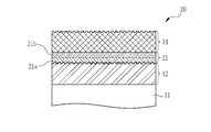
- the optical compensation plate 10 is formed by laminating a retardation compensation layer 12, an intermediate layer 13, and an antireflection layer 14 in this order on a substrate 11.
- the substrate 11 is, for example, a glass substrate.
- the substrate 11 may be a film such as TAC or PET, or an organic glass such as an acrylic resin or polycarbonate, but is preferably an inorganic glass. This is because there is almost no deterioration over time even when used in a harsh environment such as a liquid crystal projector.
- an antireflection layer is formed on the back surface of the substrate 11 (the surface opposite to the surface on which the phase difference compensation layer 12 is provided). This antireflection layer is formed of, for example, a dielectric multilayer film.
- the phase difference compensation layer 12 is a layer made of an obliquely deposited film formed by vapor-depositing an inorganic material with respect to the substrate 11 from an oblique direction, and a columnar structure is erected with an inclination with respect to the surface of the substrate 11. Has a fine structure. Due to the structural birefringence based on the inclined columnar structure, a predetermined phase difference is given to the light transmitted through the phase difference compensation layer 12. Thereby, the optical compensator 10 functions as an O plate that compensates for a phase difference caused by a pretilt of liquid crystal molecules of the VA liquid crystal panel.
- the individual columnar structures forming the retardation compensation layer 12 are on the order of, for example, several nm to several hundred nm, and parameters such as the inclination angle of the columnar structure, the stand density, and the thickness of the retardation compensation layer 12 are as follows. It is determined according to the magnitude of the phase difference to be compensated by the optical compensator 10 and suitability for manufacturing.
- the inorganic material for forming the oblique vapor deposition film of the phase difference compensation layer 12 is arbitrary. For example, tantalum pentoxide (Ta 2 O 5 ), niobium pentoxide (Nb 2 O 5 ), titanium dioxide (TiO 2 ), Silicon dioxide (SiO 2 ) or the like can be used.
- the intermediate layer 13 is made of the same material as that of either the retardation compensation layer 12 or the antireflection layer 14 or a material having an intermediate refractive index between the retardation compensation layer 12 and the antireflection layer 14. It is formed.
- the intermediate layer 13 is a dense film (so-called solid film) that does not have a fine internal structure like the retardation compensation layer 12 or the antireflection layer 14. That is, the intermediate layer 13 is formed by a normal vacuum evaporation method, CVD, or the like in which material particles are uniformly deposited from a direction substantially perpendicular to the surface of the substrate 11.
- the intermediate layer 13 is formed of the same material (Ta 2 O 5 or the like) as the retardation compensation layer 12, after the retardation compensation layer 12 is formed on the surface of the substrate 11, the surface of the retardation compensation layer 12 is deposited.
- the intermediate layer 13 can be formed by facing the source and performing deposition while rotating the substrate 11.
- a vapor deposition source of the same material as the antireflection layer 14 is prepared in the vapor deposition apparatus for forming the retardation compensation layer 12.
- the intermediate layer 13 made of the same material as that of the antireflection layer 14 can be formed by performing vapor deposition with the surface of the phase difference compensation layer 12 facing the vapor deposition source in the same manner as described above.
- the antireflection layer 14 is formed of, for example, zinc oxide (ZnO), alumina (Al 2 O 3 ), or the like, and has a network-like porous structure in which rod-like (or needle-like) crystals are intertwined and bonded.
- a concavo-convex structure on the order of several wavelengths severe nm to several hundred nm
- the antireflection layer 14 also exhibits an antireflection effect due to the concavo-convex structure on one surface, based on the same principle as the moth-eye structure.
- a solution containing zinc nitrate and ethylenediamine may be applied to the surface of the intermediate layer 13 and the solvent may be evaporated to deposit zinc oxide.
- the substrate 11 provided with the retardation compensation layer 12 and the intermediate layer 13 may be immersed in a solution containing zinc nitrate and ethylenediamine, and zinc oxide may be deposited while heating.
- alumina after forming an alumina thin film on the intermediate
- the optical compensation plate 10 functions as an O plate by the phase difference compensation layer 12 and the antireflection layer 14 is provided, so that surface reflection can be suppressed.
- both the phase difference compensation layer 12 and the antireflection layer 14 have a fine internal structure. The nature is bad. For this reason, manufacture is difficult and even if it can be manufactured, it becomes high-cost. Also, it is difficult to use in a harsh environment such as a liquid crystal projector.
- the optical compensation plate 10 by providing the dense intermediate layer 13 between the retardation compensation layer 12 and the antireflection layer 14, adhesion between the retardation compensation layer 12, the intermediate layer 13, and the intermediate layer 13 is reflected. The adhesion of the prevention layer 14 is enhanced. That is, since the optical compensation plate 10 has good adhesion between the retardation compensation layer 12 and the antireflection layer 14 due to the intermediate layer 13, it is excellent in manufacturing suitability and can withstand use in harsh environments such as a liquid crystal projector.
- the optical compensator 10 has irregularities due to the mesh porous structure of the antireflection layer 14 exposed on the surface, dust and dust are difficult to adhere. Since zinc oxide has conductivity, when zinc oxide is used for the antireflection layer 14, the optical compensator 10 is prevented from being charged, and dust and dust are difficult to adsorb.
- an optical compensation plate 10 ZnO is used for the antireflection coating layer 14
- an optical compensation for comparison in which an antireflection layer made of a dielectric multilayer film is provided on the retardation compensation layer 12 are used.
- a board was produced. Then, after rubbing the surface of each antireflection layer with a cloth to charge it, place beads (10 ⁇ m ⁇ ) for dustproof test, wipe off the excess unadsorbed beads, and set the number of adsorption in an area of 3 ⁇ 3 mm. Counted.
- this dustproof evaluation was repeated several times. Then, in the case of the optical compensator 10, the number of beads attached was approximately 300 or less, whereas in the comparative optical compensator, it was approximately 500 or more. This also shows that the optical compensator 10 has improved dust resistance compared to the conventional one.
- the intermediate layer 13 is formed of one film made of the same material as either the phase difference compensation layer 12 or the antireflection layer 14, but the optical compensation plate shown in FIG.
- the intermediate layer 21 is preferably formed of two thin films, the first thin film 21a and the second thin film 22b.
- the first thin film 21 a in contact with the retardation compensation layer 12 is a dense film made of the same material as the retardation compensation layer 12
- the second thin film 21 b in contact with the antireflection layer 14 is made of the same material as the antireflection layer 14. To a dense film.
- the retardation compensation layer 12 since the retardation compensation layer 12, the first thin film 21a, the second thin film 21b, and the antireflection layer 14 are formed of the same material, adhesion is better than that of other materials. Even if the retardation compensation layer 12 or the antireflection layer 14 has a fine internal structure, the first thin film 21a and the second thin film 21b are both dense films, and therefore, between the intermediate layer 21 and the retardation compensation layer 12. Good adhesion can be obtained, and good adhesion can be obtained between the intermediate layer 21 and the antireflection layer 14.
- the intermediate layer 21 has a two-layer configuration of the first thin film 21a and the second thin film 21b as in the optical compensation plate 20
- the retardation compensation layer is further increased than the optical compensation plate 10 of the first embodiment. 12 and the antireflection film layer 14 are improved in adhesion.
- the intermediate layer 21 has a two-layer structure of a first thin film 21a and a second thin film 21b.
- the intermediate layer 21 has a three-layer dielectric multilayer film (first dielectric). Body multilayer film layer).
- a third thin film 28 is added between the first thin film 21a and the second thin film 21b as in the intermediate layer 27 of the optical compensation plate 26 shown in FIG.
- the material and the number of films of the third thin film 28 are determined so as to have an intermediate refractive index between the first thin film 21a and the second thin film 21b, and the difference in refractive index between the first thin film 21a and the second thin film 21b is alleviated. It is preferable to do.
- the intermediate layer 27 maintains the adhesion with the retardation compensation layer 12 and the adhesion with the antireflection film layer 14 while maintaining the interface between the first thin film 21 a and the second thin film 21 b of the optical compensation plate 20. Reflection at can also be suppressed.
- the intermediate layer 21 is composed of four or more films, the number of thin films provided between the first thin film 21a and the second thin film 21b may be increased.
- a layer made of a dielectric multilayer film that functions as a negative C plate between the first thin film 21a and the second thin film 21b. (Second dielectric multilayer film layer) may be provided.
- the negative C plate is formed by alternately laminating at least two kinds of dielectric thin films having different refractive indexes.
- the degree of freedom in design is improved as compared with the case where the phase difference compensation is performed only by the phase difference compensation layer 12, so that a more accurate phase difference is achieved. Compensation is possible.
- the negative C plate is inclined with respect to the optical axis while improving the accuracy of phase difference compensation.
- the space for the liquid crystal projector can be reduced, and the liquid crystal projector can be made smaller or thinner.
- the optical compensation plate 20 is charged and easily absorbs dust and dust.
- a negative C is provided between the first thin film 21a and the second thin film 21b.
- the antireflection layer 14 it is preferable to form the antireflection layer 14 with conductive zinc oxide in order to prevent the optical compensation plate 20 from being charged.
- a dielectric multilayer film layer functioning as a negative C plate may be formed in the entire intermediate layer 21, that is, the first thin film 21a and the second thin film 21b and the entire dielectric multilayer film provided therebetween.
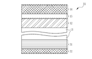
- the optical compensation plate 10 having the intermediate layer 13 formed of one film as in the optical compensation plate 10 of the first embodiment is provided with a negative C plate function, for example, the optical compensation plate 30 shown in FIG.
- the dielectric multilayer film layer 31 forming the negative C plate may be provided between the substrate 11 and the retardation compensation layer 12.
- the dielectric multilayer film layer 31 that functions as a negative C plate is provided on the back surface of the substrate 11 (the surface opposite to the surface on which the phase difference compensation layer 12 is provided). May be.
- An antireflection layer 32 is provided on the upper side of the dielectric multilayer film layer 31 (on the opposite side of the substrate 11).
- the antireflection layer 32 may be the same as that provided on the back side of each of the optical compensators 10, 20, 26, and 30 of the first and second embodiments, or has a moth-eye structure (or a structure similar to a moth-eye structure). You may have.
- the antireflection layer 32 has a network-like porous structure similar to that of the antireflection layer 14.
- the intermediate layer 13 is made of the same material as either the phase difference compensation layer 12 or the antireflection layer 14 as in the optical compensation plate 10 of the first embodiment. It may be formed by a single film, or a two-film configuration of the first thin film 21a and the second thin film 21b as in the optical compensation plate 20 of the second embodiment. Further, like the intermediate layer 27 of the optical compensation plate 26, a third thin film 28 is added between the first thin film 21a and the second thin film 21b (see FIG. 3), and the reflection at the interface between the first thin film 21a and the second thin film 21b. May also be suppressed.
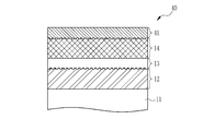
- the antireflection layer 14 having a mesh-like porous structure is exposed on the surface, but the optical compensation plate 40 shown in FIG.
- the oil resistant coating 41 is made of, for example, magnesium fluoride (MgF 2 ).
- the oil resistant coating 41 may be a fluororesin.
- the optical compensators 10, 20, 26, 30, 33 are usually used in places that are not directly touched by humans. For example, during maintenance of the liquid crystal projector, the optical compensators 10, 20, 26 are mistakenly handled by service personnel. , 30, 33 may cause oils and fats to adhere. In this case, it is difficult to completely wipe off the oil or the like, and the normal phase difference compensation effect cannot be obtained due to the remaining oil or the like. Moreover, when the remaining fats and oils permeate the retardation compensation layer 12, the retardation compensation performance is further deteriorated. For this reason, when the optical compensators 10, 20, 26, 30, 33 are used in a liquid crystal projector, the contrast performance deteriorates.
- the phase difference compensation element 40 is erroneously touched, and even if oils and fats adhere, wiping is facilitated, and the remaining oil and fats are reduced. Can be minimized. Also, when the optical compensator 40 is incorporated in a liquid crystal projector, the optical compensators 10, 20, 26, 30, 33 may be touched by mistake. In this case as well, the deterioration of the phase difference compensation performance is minimized. Therefore, by using the optical compensator 40 provided with the oil-resistant coating 41, the yield can be improved and the assembly cost can be reduced.
- the oil-resistant coating 41 is drawn thick, but it is preferable to provide the oil-resistant coating 41 thinly so as not to eliminate surface irregularities due to the mesh-like porous structure. This is because, as described above, the dustproof property is also improved by the unevenness of the surface. However, even if the oil-resistant coating 41 is formed thick enough to flatten the surface, if the material of the oil-resistant coating 41 does not penetrate into the antireflection layer 14, the antireflection performance of the antireflection layer 14 is almost the same. There is no change.
- the oil-resistant coating 41 is provided on the optical compensator 10 of the first embodiment, but each of the optical compensators 20, 26, 30, 33 of the second and third embodiments. The same applies to the above case, and it is preferable to provide the oil-resistant coating 41 on the antireflection layer 14.
- the antireflection layer 14 has a mesh-like porous structure similar to the moth-eye structure.
- the moth-eye structure itself in which rod-like crystals such as zinc oxide are grown almost perpendicularly to the surface may be used.
- an antireflection layer made of a dielectric multilayer film is provided on the back side of the substrate 11.
- the antireflection layer provided on the back surface of the substrate 11 may be an antireflection layer having a mesh-like porous structure similar to the moth-eye structure.
- an antireflection film layer having a moth-eye structure may be used.
- the optical compensation plates 10, 20, 26, 30, 33, and 40 are particularly suitable for a liquid crystal projector that uses a VA liquid crystal panel. If it is between a polarizing plate (polarizer) that restricts the polarization state of light incident on the liquid crystal panel and a polarizing plate (analyzer) that restricts the polarization state of light emitted from the liquid crystal panel, Arrangement is arbitrary.
- the liquid crystal panel may be a transmission type or a reflection type.
- the optical compensation plates 10, 20, 26, 30, 33, and 40 may be used for a liquid crystal display that directly observes a display image. If the optical compensators 10, 20, 26, 30, 33, 40 are used in the liquid crystal display, the viewing angle can be improved.
Landscapes
- Physics & Mathematics (AREA)
- General Physics & Mathematics (AREA)
- Optics & Photonics (AREA)
- Nonlinear Science (AREA)
- Chemical & Material Sciences (AREA)
- Mathematical Physics (AREA)
- Crystallography & Structural Chemistry (AREA)
- Chemical Kinetics & Catalysis (AREA)
- Polarising Elements (AREA)
- Liquid Crystal (AREA)
- Projection Apparatus (AREA)
- Surface Treatment Of Optical Elements (AREA)
- Laminated Bodies (AREA)
Description
図1に示すように、光学補償板10は、基板11上に、位相差補償層12、中間層13、反射防止層14をこの順に積層して形成される。
第1実施形態の光学補償板10では、中間層13を、位相差補償層12または反射防止層14のいずれかと同じ材料からなる一つの膜で形成しているが、図2に示す光学補償板20のように、中間層21を第1薄膜21aと第2薄膜22bの2つの薄膜で形成することが好ましい。この場合、位相差補償層12に接する第1薄膜21aは、位相差補償層12と同じ材料からなる稠密膜にし、反射防止層14に接する第2薄膜21bは、反射防止層14と同じ材料からなる稠密膜にする。
第2実施形態の光学補償板20では、中間層21を第1薄膜21aと第2薄膜21bの二膜構成にしているが、中間層21を三膜構成の誘電体多層膜層(第1誘電体多層膜層)で構成しても良い。この場合、図3に示す光学補償板26の中間層27ように、第1薄膜21aと第2薄膜21bの間に第3薄膜28を加える。そして、この第3薄膜28は、第1薄膜21aと第2薄膜21bの中間の屈折率になるように材料や膜数を決定し、第1薄膜21aと第2薄膜21bの屈折率差を緩和することが好ましい。こうすると、中間層27は、位相差補償層12との密着性及び反射防止膜層14との密着性を良好に維持しつつ、光学補償板20の第1薄膜21aと第2薄膜21bの界面における反射も抑制することができる。中間層21を四膜以上で構成する場合には、第1薄膜21aと第2薄膜21bの間に設ける薄膜数を増やせば良い。
第1~第3実施形態の各位相差補償板10,20,26,30,33では、網目状多孔構造の反射防止層14が表面に露呈されているが、図6に示す光学補償板40のように、反射防止層14に耐油性コーティング41を施しておくことが好ましい。耐油性コーティング41は、例えば、フッ化マグネシウム(MgF2)で形成される。また、耐油性コーティング41は、フッ素樹脂でも良い。
11 基板
12 位相差補償層
13,21 中間層
14 反射防止層
31 誘電体多層膜層
41 耐油性コーティング
Claims (11)
- 基板の表面に無機材料を斜方蒸着して形成され、前記基板の表面に対して傾斜した柱状構造が林立している微細構造を有する位相差補償層と、
前記位相差補償層の上側に設けられ、凹凸構造が一面に一様に形成された反射防止層と、
を備える光学補償板。 - 前記反射防止層が酸化亜鉛で形成される請求の範囲第1項記載の光学補償板。
- 前記反射防止層が網目状多孔構造である請求の範囲第1項記載の光学補償板。
- 前記位相差補償層と前記反射防止層との間に、稠密膜で形成された中間層を備える請求の範囲第1項記載の光学補償板。
- 少なくとも2種類以上の屈折率が異なる誘電体薄膜を交互に積層して形成された第1誘電体多層膜層が、前記基板と前記位相差補償層との間に設けられている請求の範囲第1項記載の光学補償板。
- 前記中間層が1つの膜で形成される場合、前記中間層が前記位相差補償層または前記反射防止層と同じ材料で形成されている請求の範囲第4項記載の光学補償板。
- 前記中間層は、前記位相差補償層と同じ材料によって形成された第1稠密膜と、前記反射防止層と同じ材料で形成された第2稠密膜とを備え、
前記第1稠密膜は、前記中間層の最も前記位相差補償層側に設けられ、
前記第2稠密膜は、前記中間層の最も前記反射防止層側に設けられている請求の範囲第4項記載の光学補償板。 - 前記中間層は、前記第1稠密膜と前記第2稠密膜との間に、互いに屈折率が異なる2種類以上の誘電体薄膜を積層して形成された第2誘電体多層膜層を備える請求の範囲第7項記載の光学補償板。
- 前記反射防止層の上側に、耐油性コーティングを備える請求の範囲第7項記載の光学補償板。
- 前記耐油性コーティングは、フッ化マグネシウムで形成されている請求の範囲第10項記載の光学補償板。
- 前記反射防止層が、棒状または針状の結晶が表面に対して垂直に林立したモスアイ構造を有する請求の範囲第3項記載の光学補償板。
Priority Applications (4)
| Application Number | Priority Date | Filing Date | Title |
|---|---|---|---|
| JP2014538295A JP5816378B2 (ja) | 2012-09-28 | 2013-08-27 | 光学補償板 |
| DE112013004797.7T DE112013004797B4 (de) | 2012-09-28 | 2013-08-27 | Optische Kompensationsplatte |
| CN201380050870.3A CN104737040B (zh) | 2012-09-28 | 2013-08-27 | 光学补偿板 |
| US14/663,477 US10101516B2 (en) | 2012-09-28 | 2015-03-20 | Optical compensation plate |
Applications Claiming Priority (2)
| Application Number | Priority Date | Filing Date | Title |
|---|---|---|---|
| JP2012218048 | 2012-09-28 | ||
| JP2012-218048 | 2012-09-28 |
Related Child Applications (1)
| Application Number | Title | Priority Date | Filing Date |
|---|---|---|---|
| US14/663,477 Continuation US10101516B2 (en) | 2012-09-28 | 2015-03-20 | Optical compensation plate |
Publications (1)
| Publication Number | Publication Date |
|---|---|
| WO2014050408A1 true WO2014050408A1 (ja) | 2014-04-03 |
Family
ID=50387817
Family Applications (1)
| Application Number | Title | Priority Date | Filing Date |
|---|---|---|---|
| PCT/JP2013/072855 Ceased WO2014050408A1 (ja) | 2012-09-28 | 2013-08-27 | 光学補償板 |
Country Status (5)
| Country | Link |
|---|---|
| US (1) | US10101516B2 (ja) |
| JP (1) | JP5816378B2 (ja) |
| CN (1) | CN104737040B (ja) |
| DE (1) | DE112013004797B4 (ja) |
| WO (1) | WO2014050408A1 (ja) |
Cited By (4)
| Publication number | Priority date | Publication date | Assignee | Title |
|---|---|---|---|---|
| US20150162946A1 (en) * | 2013-12-06 | 2015-06-11 | Shenzhen China Star Optoelectronics Technology Co., Ltd. | Glass substrate for display and manufacturing method thereof |
| KR101778836B1 (ko) | 2014-11-27 | 2017-09-26 | 주식회사 엘지화학 | 광학 필름 및 이의 제조방법 |
| JPWO2017056598A1 (ja) * | 2015-09-29 | 2017-12-14 | 富士フイルム株式会社 | 親水性多層膜及びその製造方法、並びに、撮像システム |
| JP2022121424A (ja) * | 2016-10-04 | 2022-08-19 | 株式会社半導体エネルギー研究所 | 表示装置 |
Families Citing this family (5)
| Publication number | Priority date | Publication date | Assignee | Title |
|---|---|---|---|---|
| JP7200984B2 (ja) * | 2018-02-20 | 2023-01-10 | ソニーグループ株式会社 | 光学補償素子、液晶表示装置および投射型表示装置 |
| JP7236225B2 (ja) * | 2018-05-31 | 2023-03-09 | デクセリアルズ株式会社 | 位相差補償素子、液晶表示装置および投射型画像表示装置 |
| JP7236230B2 (ja) * | 2018-09-07 | 2023-03-09 | デクセリアルズ株式会社 | 光学素子、液晶表示装置および投射型画像表示装置 |
| CN208721825U (zh) * | 2018-09-30 | 2019-04-09 | 惠科股份有限公司 | 偏光板、显示面板及显示装置 |
| CN109143446A (zh) * | 2018-09-30 | 2019-01-04 | 惠科股份有限公司 | 偏光板及显示装置 |
Citations (12)
| Publication number | Priority date | Publication date | Assignee | Title |
|---|---|---|---|---|
| JPH08122523A (ja) * | 1994-10-28 | 1996-05-17 | Matsushita Electric Ind Co Ltd | 位相差板 |
| JPH08211202A (ja) * | 1995-02-07 | 1996-08-20 | Hitachi Ltd | 撥水撥油性超微粒子を有する光透過板およびその製造方法 |
| JPH09297214A (ja) * | 1996-05-08 | 1997-11-18 | Matsushita Electric Ind Co Ltd | 偏光素子 |
| JPH11281802A (ja) * | 1998-03-31 | 1999-10-15 | Fuji Photo Film Co Ltd | 反射防止膜、反射防止部材及び反射防止部材の製造方法 |
| JP2000052492A (ja) * | 1998-08-12 | 2000-02-22 | Toppan Printing Co Ltd | 反射防止積層体、光学機能性積層体、および表示装置 |
| JP2001183506A (ja) * | 1999-12-24 | 2001-07-06 | Sony Corp | 光学素子及び表示装置 |
| JP2001228330A (ja) * | 2000-02-17 | 2001-08-24 | Sankyo Seiki Mfg Co Ltd | 複屈折板 |
| JP2006119444A (ja) * | 2004-10-22 | 2006-05-11 | Fuji Photo Film Co Ltd | 位相差補償素子およびそれを用いた液晶装置 |
| JP2006133617A (ja) * | 2004-11-08 | 2006-05-25 | Matsushita Electric Ind Co Ltd | 反射防止構造体を有する部材およびその製造方法 |
| JP2006171328A (ja) * | 2004-12-15 | 2006-06-29 | Fuji Photo Film Co Ltd | 位相差補償素子、光変調システム、液晶表示装置及び液晶プロジェクタ |
| JP2006308832A (ja) * | 2005-04-28 | 2006-11-09 | Asahi Kasei Corp | 反射防止膜 |
| WO2011135976A1 (ja) * | 2010-04-28 | 2011-11-03 | シャープ株式会社 | 型および型の製造方法 |
Family Cites Families (4)
| Publication number | Priority date | Publication date | Assignee | Title |
|---|---|---|---|---|
| TW412644B (en) * | 1998-07-28 | 2000-11-21 | Sumitomo Chemical Co | Front panel for display |
| JP2006145884A (ja) * | 2004-11-19 | 2006-06-08 | Sony Corp | 反射型偏光子及びカラー液晶表示装置 |
| WO2006064956A1 (en) * | 2004-12-15 | 2006-06-22 | Fujifilm Corporation | Phase difference compensator, light modurating system, liquid crystal display and liquid crystal projector |
| TWI427374B (zh) | 2006-12-27 | 2014-02-21 | Fujifilm Corp | 遲延度補償元件、垂直配向向列型液晶顯示裝置、及液晶投影機 |
-
2013
- 2013-08-27 DE DE112013004797.7T patent/DE112013004797B4/de active Active
- 2013-08-27 CN CN201380050870.3A patent/CN104737040B/zh active Active
- 2013-08-27 JP JP2014538295A patent/JP5816378B2/ja active Active
- 2013-08-27 WO PCT/JP2013/072855 patent/WO2014050408A1/ja not_active Ceased
-
2015
- 2015-03-20 US US14/663,477 patent/US10101516B2/en active Active
Patent Citations (12)
| Publication number | Priority date | Publication date | Assignee | Title |
|---|---|---|---|---|
| JPH08122523A (ja) * | 1994-10-28 | 1996-05-17 | Matsushita Electric Ind Co Ltd | 位相差板 |
| JPH08211202A (ja) * | 1995-02-07 | 1996-08-20 | Hitachi Ltd | 撥水撥油性超微粒子を有する光透過板およびその製造方法 |
| JPH09297214A (ja) * | 1996-05-08 | 1997-11-18 | Matsushita Electric Ind Co Ltd | 偏光素子 |
| JPH11281802A (ja) * | 1998-03-31 | 1999-10-15 | Fuji Photo Film Co Ltd | 反射防止膜、反射防止部材及び反射防止部材の製造方法 |
| JP2000052492A (ja) * | 1998-08-12 | 2000-02-22 | Toppan Printing Co Ltd | 反射防止積層体、光学機能性積層体、および表示装置 |
| JP2001183506A (ja) * | 1999-12-24 | 2001-07-06 | Sony Corp | 光学素子及び表示装置 |
| JP2001228330A (ja) * | 2000-02-17 | 2001-08-24 | Sankyo Seiki Mfg Co Ltd | 複屈折板 |
| JP2006119444A (ja) * | 2004-10-22 | 2006-05-11 | Fuji Photo Film Co Ltd | 位相差補償素子およびそれを用いた液晶装置 |
| JP2006133617A (ja) * | 2004-11-08 | 2006-05-25 | Matsushita Electric Ind Co Ltd | 反射防止構造体を有する部材およびその製造方法 |
| JP2006171328A (ja) * | 2004-12-15 | 2006-06-29 | Fuji Photo Film Co Ltd | 位相差補償素子、光変調システム、液晶表示装置及び液晶プロジェクタ |
| JP2006308832A (ja) * | 2005-04-28 | 2006-11-09 | Asahi Kasei Corp | 反射防止膜 |
| WO2011135976A1 (ja) * | 2010-04-28 | 2011-11-03 | シャープ株式会社 | 型および型の製造方法 |
Cited By (7)
| Publication number | Priority date | Publication date | Assignee | Title |
|---|---|---|---|---|
| US20150162946A1 (en) * | 2013-12-06 | 2015-06-11 | Shenzhen China Star Optoelectronics Technology Co., Ltd. | Glass substrate for display and manufacturing method thereof |
| US9382622B2 (en) * | 2013-12-06 | 2016-07-05 | Shenzhen China Star Optoelectronics Technology Co., Ltd. | Glass substrate for display and manufacturing method thereof |
| KR101778836B1 (ko) | 2014-11-27 | 2017-09-26 | 주식회사 엘지화학 | 광학 필름 및 이의 제조방법 |
| JPWO2017056598A1 (ja) * | 2015-09-29 | 2017-12-14 | 富士フイルム株式会社 | 親水性多層膜及びその製造方法、並びに、撮像システム |
| US10732325B2 (en) | 2015-09-29 | 2020-08-04 | Fujifilm Corporation | Hydrophilic multilayer film and method for producing same, and imaging system |
| JP2022121424A (ja) * | 2016-10-04 | 2022-08-19 | 株式会社半導体エネルギー研究所 | 表示装置 |
| JP7274645B2 (ja) | 2016-10-04 | 2023-05-16 | 株式会社半導体エネルギー研究所 | 表示装置 |
Also Published As
| Publication number | Publication date |
|---|---|
| CN104737040B (zh) | 2017-02-01 |
| DE112013004797B4 (de) | 2017-02-02 |
| JP5816378B2 (ja) | 2015-11-18 |
| US10101516B2 (en) | 2018-10-16 |
| CN104737040A (zh) | 2015-06-24 |
| DE112013004797T5 (de) | 2015-07-23 |
| US20150192723A1 (en) | 2015-07-09 |
| JPWO2014050408A1 (ja) | 2016-08-22 |
Similar Documents
| Publication | Publication Date | Title |
|---|---|---|
| JP5816378B2 (ja) | 光学補償板 | |
| CN103097995B (zh) | 触摸面板器件、及带有触摸面板器件的显示装置 | |
| JP6735310B2 (ja) | 偏光板及びこれを備える液晶表示装置 | |
| TWI236547B (en) | Optical multilayer-film filter, method for fabricating optical multilayer-film filter, optical low-pass filter, and electronic apparatus | |
| US9651714B2 (en) | Antireflection multilayer film | |
| CN101203778B (zh) | 用于偏振片的保护膜 | |
| JP5350642B2 (ja) | ガスバリア層付フィルム | |
| WO2013179951A1 (ja) | 光学積層体、偏光板、偏光板の製造方法、画像表示装置、画像表示装置の製造方法及び画像表示装置の視認性改善方法 | |
| JP2016510904A (ja) | 光学フィルム | |
| JP2019132973A (ja) | 反射スクリーン、映像表示装置 | |
| US20210231997A1 (en) | Light control film and liquid crystal display device | |
| CN104062798A (zh) | 显示设备 | |
| US8964139B2 (en) | Multifunctional optical filter for stereoscopic display device and stereoscopic display device comprising the same | |
| WO2013179813A1 (ja) | 表示装置 | |
| US11269218B2 (en) | Phase difference compensation element, liquid crystal display device and projection type image display device | |
| TW201213897A (en) | Patterned retarder laminated composite polarizing plate and display apparatus using the same | |
| JP2008268466A (ja) | 位相差補償素子及びその製造方法 | |
| KR101321871B1 (ko) | 편광판, 편광판의 제조 방법 및 이를 갖는 액정 표시 장치 | |
| JP2019066531A (ja) | 液晶モジュール | |
| JPH0667172A (ja) | 液晶表示素子及びその製造方法 | |
| US10795197B2 (en) | Liquid crystal panel | |
| CN106033158B (zh) | 相位差元件、液晶显示装置以及投影型图像显示装置 | |
| CN112105974B (zh) | 相位差补偿元件、液晶显示装置、以及投射型图像显示装置 | |
| CN103308966A (zh) | 光学构件及显示系统 | |
| JPWO2018116895A1 (ja) | 液晶パネル |
Legal Events
| Date | Code | Title | Description |
|---|---|---|---|
| 121 | Ep: the epo has been informed by wipo that ep was designated in this application |
Ref document number: 13841362 Country of ref document: EP Kind code of ref document: A1 |
|
| DPE1 | Request for preliminary examination filed after expiration of 19th month from priority date (pct application filed from 20040101) | ||
| ENP | Entry into the national phase |
Ref document number: 2014538295 Country of ref document: JP Kind code of ref document: A |
|
| WWE | Wipo information: entry into national phase |
Ref document number: 112013004797 Country of ref document: DE Ref document number: 1120130047977 Country of ref document: DE |
|
| 122 | Ep: pct application non-entry in european phase |
Ref document number: 13841362 Country of ref document: EP Kind code of ref document: A1 |