WO2014050068A1 - 電流センサ - Google Patents
電流センサ Download PDFInfo
- Publication number
- WO2014050068A1 WO2014050068A1 PCT/JP2013/005612 JP2013005612W WO2014050068A1 WO 2014050068 A1 WO2014050068 A1 WO 2014050068A1 JP 2013005612 W JP2013005612 W JP 2013005612W WO 2014050068 A1 WO2014050068 A1 WO 2014050068A1
- Authority
- WO
- WIPO (PCT)
- Prior art keywords
- current
- current path
- magnetoelectric conversion
- magnetic flux
- flux density
- Prior art date
Links
Images


Classifications
-
- G—PHYSICS
- G01—MEASURING; TESTING
- G01R—MEASURING ELECTRIC VARIABLES; MEASURING MAGNETIC VARIABLES
- G01R19/00—Arrangements for measuring currents or voltages or for indicating presence or sign thereof
- G01R19/0092—Arrangements for measuring currents or voltages or for indicating presence or sign thereof measuring current only
-
- G—PHYSICS
- G01—MEASURING; TESTING
- G01R—MEASURING ELECTRIC VARIABLES; MEASURING MAGNETIC VARIABLES
- G01R15/00—Details of measuring arrangements of the types provided for in groups G01R17/00 - G01R29/00, G01R33/00 - G01R33/26 or G01R35/00
- G01R15/14—Adaptations providing voltage or current isolation, e.g. for high-voltage or high-current networks
- G01R15/20—Adaptations providing voltage or current isolation, e.g. for high-voltage or high-current networks using galvano-magnetic devices, e.g. Hall-effect devices, i.e. measuring a magnetic field via the interaction between a current and a magnetic field, e.g. magneto resistive or Hall effect devices
- G01R15/207—Constructional details independent of the type of device used
Definitions
- the present invention relates to a current sensor that measures a measured current flowing in various devices by using a magnetoelectric conversion element, and more particularly, to a current sensor suitable when the frequency of the measured current flowing in various devices mounted with an inverter or the like changes.
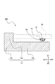
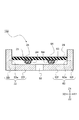
- FIG. 27 is a view for explaining the current measurement device 900 disclosed in Patent Document 1, and is a cross-sectional view showing the positional relationship between the magnetic sensor 910 and the conductor 901 to be measured.
- the current measuring device 900 is configured of a conductor to be measured 901 formed on a printed circuit board 911 and a magnetic sensor 910 (having a magnetic detection element inside) mounted on the printed circuit board 912.
- the magnetic sensor 910 detects a magnetic field 920 generated in the width direction of the conductor 901 when the current to be measured flows through the conductor 901.
- the frequency of the current to be measured flowing in such a flat shaped conductor to be measured 901 becomes high, the current to be measured is concentrated on the end of the conductor to be measured 901 by the skin effect, and the center of the conductor 901 to be measured Then, the current density decreases, and the current density increases near the end of the conductor 901 to be measured. Therefore, when the magnetic sensor 910 is disposed at the center of the conductor to be measured 901 (located at the end in FIG. 27), the magnetic field 920 near the center detected by the magnetic sensor 910 decreases and the current sensitivity of the current measuring device 900 There was a problem to say that it falls.
- the magnetic sensor 910 is provided at a position separated by a predetermined distance from the central position CL in the width direction of the conductor 901 to be measured. As a result, it is possible to provide the current measurement apparatus 900 in which the decrease in measurement sensitivity is suppressed even in the case of a high-frequency measurement current.
- the magnetic sensor 910 is disposed near the end of the conductor 901 to be measured in accordance with the frequency of the current to be measured, the same applies to other devices using the current to be measured having different frequencies.
- the frequency changes depending on the state even with an apparatus the current sensitivity measured by the current measuring device 900 is largely different, and there is a problem that accurate measurement accuracy can not be obtained.
- the case where the frequency of the current to be measured changes depending on the state is, for example, a case where the frequency of the current to be measured changes depending on states such as idling, acceleration and regenerative braking in an electric car or a hybrid car. Be
- the present invention solves the above-mentioned problem, and an object of the present invention is to provide a current sensor that can perform measurement with high accuracy even if the frequency of the current to be measured changes.
- the current sensor includes a first current path having a first flat portion and a measured current which is disposed on the first current path and flows in the first current path. And a first magnetoelectric conversion element for detecting magnetism generated in the first current path, wherein the first current path is connected to the first current path.
- a lowest frequency magnetic flux density which is a magnetic flux density in the case of flowing the measured current of the lowest frequency used in the device, provided with a conductive first convex portion along the direction in which the current flows;
- the first magnetoelectric conversion element is disposed at a position on the first current path where the maximum frequency magnetic flux density, which is the magnetic flux density in the case of flowing the measured current of the highest frequency to be used, substantially matches It is characterized.
- the target of the lowest frequency used in the device is The lowest frequency magnetic flux density, which is the magnetic flux density when the measurement current flows, and the highest frequency magnetic flux density, which is the magnetic flux density when the highest frequency of the measured current flows, can be made closer to each other. Therefore, the first magnetoelectric conversion element can be disposed at a position where the change in magnetic flux density due to the change in frequency is small. As a result, even if the frequency of the current to be measured changes, the lowest frequency magnetic flux density and the highest frequency magnetic flux density do not differ significantly, so that the current value can be measured accurately.
- the current sensor of the present invention is characterized in that the first convex portion is erected from any one end of the first flat portion.
- the first magnetoelectric conversion element can be disposed closer to the center of the first current path, and the magnetic sensor (magnetoelectric conversion element) 910 is disposed outside the measured conductor (current path) 901 as in the conventional example.
- the influence of the external magnetic field from the adjacent current paths and the like can be reduced as compared with the case where
- the first flat portion and the first convex portion are integrally formed by bending a metal plate.
- a second current path having a second flat portion and a magnetism generated when the current to be measured is disposed on the second current path and flows in the second current path.
- a connecting portion for connecting one ends of the first current path and the second current path to each other, and the first current path and the second current path are connected in parallel
- the other end of the second current path is connected to the device, and the second current path is provided with a conductive second convex portion along the direction in which the current to be measured flows.
- the lowest frequency magnetic flux density which is the magnetic flux density when the measured current of the lowest frequency used in the device flows, and the highest frequency, the magnetic flux density when the measured current of the highest frequency used in the device flows
- the second current path substantially matching the magnetic flux density
- the second magnetoelectric conversion element is disposed at the position of the first convex portion, and the first convex portion is erected from the end portion on the side away from the second current path, and the second convex portion
- the first magnetoelectric conversion element and the second magnetoelectric conversion element are provided on the same substrate, and the first magnetoelectric conversion element and the second magnetoelectric conversion element are provided on the same substrate.
- the second magnetoelectric conversion element can be disposed at a position where the change in magnetic flux density due to the change in frequency is small. As a result, even if the frequency of the current to be measured changes, the lowest frequency magnetic flux density and the highest frequency magnetic flux density do not greatly differ, so that the current value can be measured with high accuracy also in the second current path.
- the first magnetoelectric conversion element and the second magnetoelectric conversion element are respectively provided on the same substrate, when current flows in the external magnetic field or the current path (the first current path and the second current path) The influence of the generated internal magnetic field appears with the same strength in the two magnetoelectric transducers (the first magnetoelectric transducer and the second magnetoelectric transducer). Therefore, by differentially processing the outputs from the two magnetoelectric conversion elements (the first magnetoelectric conversion element and the second magnetoelectric conversion element), the influence of the magnetic field can be canceled more accurately. This can reduce the deterioration of the measurement accuracy of the current sensor.
- the current sensor of the present invention has at least two or more of the first magnetoelectric conversion elements and at least two of the second magnetoelectric conversion elements, and at least one of the first magnetoelectric conversion elements is the first one.
- the first flat shape in which at least one of the first magnetoelectric conversion elements is not provided while the first convex portion is disposed at the first position of the first flat portion on which the convex portion is provided.
- a third position of the second portion, and at least one of the second magnetoelectric conversion elements is disposed at a second position of the second flat-shaped portion on which the second convex portion is erected; It is characterized in that at least one of the two magnetoelectric conversion elements is disposed at a fourth position of the second flat portion where the second convex portion is not provided.
- the first magnetoelectric conversion element disposed at the first position of the first current path where the first convex portion is erected and the second position of the second current path where the second convex portion is erected And the second magnetoelectric conversion element, and the third position of the first current path where the first convex portion is not erected and the first magnetoelectric conversion provided at the fourth position of the second current path where the second convex portion is not erected
- the element and the second magnetoelectric conversion element are separately disposed.
- the magnetic amounts detected by the first magnetoelectric conversion element and the second magnetoelectric conversion element disposed at the first position and the second position, and the first magnetoelectric conversion element disposed at the third position and the fourth position The absolute amount of the amount of magnetism detected by the second magnetoelectric conversion element differs. Therefore, the first magnetoelectric conversion element and the second magnetoelectric conversion element disposed at the first position and the second position are disposed at the third position and the fourth position for high current measurement, and The second magnetoelectric conversion element can be used separately for constant current measurement. As a result, in the case of high current measurement, measurement can be performed in a wide range, and in the case of low current measurement, measurement can be performed with high accuracy.
- the first flat portion, the first convex portion, the connection portion, the second flat portion and the second convex portion are integrally formed by bending a metal plate. It is characterized by
- the first current path is provided with the conductive first convex portion that is long along the direction in which the current to be measured flows, the lowest frequency used in the device (the device to be measured)
- the lowest frequency magnetic flux density which is the magnetic flux density when the current to be measured flows
- the highest frequency magnetic flux density which is the magnetic flux density when the current to be measured at the highest frequency flows
- the first magnetoelectric conversion element can be disposed at a position where the change in magnetic flux density due to the change in frequency is small.
- FIG. 18A is a cross-sectional view taken along line XVII-XVII shown in FIG. 17
- FIG. 18B is a block diagram illustrating the current sensor of the third embodiment of the present invention. It is a cross-sectional view taken along line XVIII-XVIII. It is a top view of the 1st current course of the model used for simulation of the current sensor of a 3rd embodiment of the present invention, the 2nd current course, and a connection part.
- FIG. 22 (a) is a simulation result in the direction of XX-XX line shown in FIG. 19 in the current sensor of the third embodiment of the present invention, and FIG. It is a simulation result of the comparative example compared with a).
- FIG. 22 (a) is a simulation result in the direction of XX-XX line shown in FIG. 19 in the current sensor of the third embodiment of the present invention, and FIG. It is a simulation result of the comparative example compared with a).
- FIG. 23 is a view for explaining a modification of the current sensor according to the first embodiment of the present invention, and FIG. 23 (a) is a model of Modification 1, and FIG. 23 (b) is a model of Modification 2; 23 (c) is a model diagram of the third modification, and FIG. 23 (d) is a model diagram of the fourth modification. It is a figure explaining the modification of the current sensor of a 1st embodiment of the present invention, and Drawing 24 (a) is a top view of modification 5; Drawing 24 (b) is a top view of modification 6 It is.
- FIG.25 (a) is a perspective view of the modification 7
- FIG.25 (b) is a perspective of the modification 8.
- FIG. 25 (c) is a perspective view of Modification 9
- FIG. FIG. 26A is a view comparing with a current sensor according to an embodiment of the present invention
- FIG. 26A is a view of a model H101 of a comparative example used for the simulation
- FIG. 26B is a simulation of the model H101. It is a graph of a result.
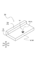
- FIG. 1 is an exploded perspective view for explaining a current sensor 101 according to a first embodiment of the present invention.
- FIG. 2 is a perspective view for explaining the current sensor 101 according to the first embodiment of the present invention.
- the insulating substrate 19 is omitted to facilitate the description.
- FIG. 3 is a configuration diagram for explaining the current sensor 101 according to the first embodiment of the present invention, and is a top view seen from the Z1 side shown in FIG.
- FIG. 4 is a configuration diagram for explaining the current sensor 101 according to the first embodiment of the present invention, and is a cross-sectional view taken along the line IV-IV shown in FIG.
- the current sensor 101 includes a first current path 12 having a first flat portion 12f, and a first current path 12 disposed on the first current path 12.
- a magnetoelectric conversion element 13 is provided.
- the insulating substrate 19 disposed opposite to the first current path 12 and, although not shown, external control for supplying power to the current sensor 101 and for taking out a signal from the current sensor 101.
- a connector is provided to connect to the device.
- the first current path 12 is made of a metal material having good conductivity such as copper (Cu), and as shown in FIGS. 1 to 4, a first flat portion 12 f and one of the first current paths 12.
- the first projection 12w is configured to have a first projection 12w erected from the end 12t, and the first projection 12w is formed along the flow direction of the current to be measured (Y direction shown in FIG. 2). There is. Further, although not shown, at both ends of the first current path 12, holding portions for connecting and fixing a current path to be measured (a current path to be measured) of a device (device to be measured) not shown. It is provided.
- the first flat portion 12 f and the first convex portion 12 w are integrally formed by bending a metal plate such as copper (Cu). Thereby, when manufacturing the 1st flat part 12f and the 1st convex part 12w, it can manufacture easily from one metal plate. By this, the current sensor 101 can be made inexpensive.
- the first magnetoelectric conversion element 13 is an element for detecting the magnetism generated when the current to be measured flows in the first current path 12 and is, for example, a magnetoresistance effect element (GMR (Giant) using a giant magnetoresistance effect. It is packaged in the magnetic sensor package 14 as shown in FIG. 4 using a Magneto Resistive) element. Further, as shown in FIGS. 2 and 3, the first magnetoelectric conversion element 13 is disposed on the first flat portion 12 f and disposed near the center of the first flat portion 12 f in the longitudinal direction. And the other end of the first current path 12. The sensitivity direction of the first magnetoelectric transducer 13 is disposed in the X direction shown in FIG.
- GMR magnetoresistance effect element
- the magnetic sensor package 14 is fabricated of a GMR element formed on a silicon substrate, and then electrically connected to a chip of the GMR element cut out and a lead terminal 14r for taking out a signal, and a thermosetting synthetic resin. Packaged and manufactured.
- the magnetic sensor package 14 is soldered to the insulating substrate 19 which is a circuit substrate by the lead terminals 14r, and is connected to an external control device via a wiring pattern and a connector (not shown).
- the first magnetoelectric conversion element 13 is packaged and disposed on the insulating substrate 19 as the magnetic sensor package 14, for example, the first magnetoelectric conversion element 13 may be disposed as it is, so-called bare chip mounting. good.
- the insulating substrate 19 uses a widely known single-sided printed wiring board, and a metal foil such as copper (Cu) provided on the base substrate is patterned on a glass-filled epoxy resin base substrate. , Forming a wiring pattern.
- a metal foil such as copper (Cu) provided on the base substrate is patterned on a glass-filled epoxy resin base substrate. , Forming a wiring pattern.
- one magnetic sensor package 14 in which the first magnetoelectric transducer 13 is packaged is mounted on the insulating substrate 19.
- a printed wiring board made of an epoxy resin containing glass is used as the insulating substrate 19, the present invention is not limited to this.
- a ceramic wiring board or a flexible wiring board may be used.
- a circuit board is preferably used as the insulating board 19.
- the present invention is not limited to the circuit board, and the magnetic sensor package 14 is mounted by overlapping the circuit board on the insulating board 19. It may be configured to
- FIG. 5 is a cross-sectional view of the first current path 12 of the model used for the simulation of the current sensor of the first embodiment of the present invention
- FIG. 5 (a) is a model A1
- 6 is a cross-sectional view of the first current path 12 of the model used in the simulation of the current sensor according to the first embodiment of the present invention
- FIG. 6 (a) is a model B1.
- b) is model B2.
- the numerical values used for this simulation (see FIGS. 5 and 6) set the entire length of the first current path 12 to 100 (mm), the entire width W 1 to 20 (mm), and the first flat portion 12f.
- the thickness T1 of each of the models was 4 (mm), and the length of the first convex portion 12 w was 100 (mm).
- the width W2 of the first protrusion 12w is 4 (mm), the thickness T2 is 4 (mm), and for the model A2, the width W2 of the first protrusion 12w is 4 (mm), and the thickness T2 is In the model B1, the width W2 of the first convex portion 12w is 6 (mm), the thickness T2 is 4 (mm), the width W2 of the first convex portion 12w is 8 (mm), and the thickness T2 of the model B1. It was 4 (mm) and was made variable.
- the current sensor 101 shown in FIGS. 1 to 4 is an embodiment of the model A1.
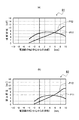
- FIG. 7 is a simulation result of the current sensor according to the first embodiment of the present invention, which is a graph corresponding to the model A1 of FIG. 5A and the model A2 of FIG. 5B.
- FIG. 8 is a simulation result of the current sensor according to the first embodiment of the present invention, which is a graph corresponding to the model B1 of FIG. 6A and the model B2 of FIG. 6B.
- the horizontal axes of the graphs in FIGS. 7 and 8 represent the width W1 of the first current path 12 and indicate the distances from the center (10 (mm) respectively on the left and right), and the vertical axes in the graphs in FIGS.
- P11 in the figure indicates the lowest frequency magnetic flux density when the frequency of the current to be measured used in the device (device to be measured) is 10 (Hz) and the lowest frequency assumed
- P2 in the figure is The frequency of the measured current used in the device (device to be measured) is 10 (kHz), which indicates the highest frequency magnetic flux density in the case of the highest frequency assumed.
- FIG. 26 is a view comparing with the current sensor 101 according to the first embodiment of the present invention
- FIG. 26 (a) is a view of a model H101 of a comparative example used for the simulation; These are graphs of the simulation result of the model H101.
- the length of the current path H12 was 100 (mm)
- the thickness H1 was 4 (mm)
- the width H2 was 20 (mm).
- the first convex is compared with the case where the magnetic flux density largely differs due to the difference between the low frequency and the high frequency of the current to be measured as shown in FIG.
- the difference between the magnetic flux density due to the difference between the low frequency and the high frequency of the current to be measured that is, the difference between the lowest frequency magnetic flux density P11 and the highest frequency magnetic flux density P2 on the first flat portion 12f not provided with the portion 12w It was getting smaller. This is considered to be because the magnetic field around the first current path 12 was changed by providing the first convex portion 12 w. Therefore, the lowest frequency magnetic flux density P11 and the highest frequency magnetic flux density P2 can be made closer to each other by providing the conductive first convex portion 12w along the direction in which the current to be measured flows, and can be made more consistent.
- the first magnetoelectric conversion element 13 be disposed at a position on the first current path 12 where the lowest frequency magnetic flux density P11 and the highest frequency magnetic flux density P2 substantially match.
- the distance from the center is approximately 7 (mm) on the first flat portion 12f where the first convex portion 12w of the first current path 12 is not provided.
- the first magnetoelectric conversion element 13 is disposed at a distance of about 6.5 (mm).
- the distance from the center is about 5.5 (on the first flat portion 12 f where the first convex portion 12 w of the first current path 12 is not provided). It is desirable to arrange the first magnetoelectric conversion element 13 at the position of mm), and in the case of the model B2, on the first flat portion 12f where the first convex portion 12w of the first current path 12 is not provided, It is desirable to arrange the first magnetoelectric conversion element 13 at a distance of about 5 (mm) from the center.
- the first magnetoelectric conversion element 13 can be disposed at a position where the change in magnetic flux density due to the change in frequency is small. Since the lowest frequency magnetic flux density P11 and the highest frequency magnetic flux density P2 do not differ greatly, it is possible to measure the current value accurately.
- the current measuring device 900 of the conventional example the position (the R portion of the peak of the highest frequency magnetic flux density P2 shown in FIG. 26B) shown in FIG. Since the magnetic sensor 910 is provided at a distance of about 9 (mm), the difference between the lowest frequency magnetic flux density P11 and the highest frequency magnetic flux density P2 is large. Therefore, when applied to another device using a measured current having a different frequency or when the frequency changes depending on the state even with the same device, the current sensitivity measured by the current measuring device 900 is largely different, and accurate measurement The accuracy can not be obtained.
- the first convex portion 12w is erected from the end 12t of the first flat portion 12f, and the height T2 and the width W2 of the first convex portion 12w are changed.
- the position where the change of the magnetic flux density accompanying the frequency change is small can be arbitrarily changed.
- the arrangement position of the 1st magnetoelectric conversion element 13 can also be set up arbitrarily.
- the position where the change in the magnetic flux density accompanying the change in the frequency is small can be changed by changing the shape of the first convex portion 12w, for example, the length or the surface shape of the corner,
- the arrangement position of the 1 magnetoelectric transducer 13 can be set arbitrarily.
- the first convex portion 12w is erected from the end 12t of the first flat portion 12f, the lowest frequency magnetic flux density P11 and the highest frequency magnetic flux density P2 are approximately The coincident position can be moved to the center side of the first current path 12.
- the first magnetoelectric conversion element 13 can be disposed closer to the center of the first current path 12 and the magnetic sensor (magnetoelectric conversion element) 910 is provided outside the measured conductor (current path) 901 as in the conventional example.
- the influence of the external magnetic field from the adjacent current paths and the like can be reduced as compared with the case where the
- the existence of this effect can solve the following problems.
- By changing the height H2 and the width W2 of the first convex portion 12w it is possible to arbitrarily change the position where the lowest frequency magnetic flux density P11 and the highest frequency magnetic flux density P2 substantially coincide with each other.
- the position where the sensor can be arranged is limited, and the current measuring device 900 as in the conventional example can solve the problem that the magnetic sensor (magnetoelectric conversion element) 910 can not be arranged at the best position.
- the first magnetoelectric conversion element 13 be disposed at a position on the first current path 12 at which the lowest frequency magnetic flux density P11 and the highest frequency magnetic flux density P2 substantially match, the lowest frequency magnetic flux density
- the first magnetoelectric conversion element 13 may be disposed at a position on the first current path 12 corresponding to a region where P11 and the maximum frequency magnetic flux density P2 become equal.
- a region where the lowest frequency magnetic flux density P11 and the highest frequency magnetic flux density P2 are equal that is, the distance from the center is 4.5 (mm) to 7
- the first magnetoelectric conversion element 13 may be disposed between 5 mm and preferably between 5.5 mm and 7 mm.
- the distance from the center is between 2.5 (mm) and 7 (mm), preferably 4.5 (mm) to 6 (mm)
- the first magnetoelectric conversion element 13 may be disposed between them.
- the first convex portion 12 w can be provided so that the region in which the lowest frequency magnetic flux density P 11 and the highest frequency magnetic flux density P 2 are equal becomes wide.
- the first magnetoelectric conversion element 13 can be disposed arbitrarily within the range of this region, so that, for example, even in the case where the position where the current sensor 101 can be disposed is limited in the on-vehicle application, the first The magnetoelectric conversion element 13 can be disposed at the best position.
- the first current path 12 is provided with the conductive first convex portion 12 w which is long along the flowing direction of the current to be measured.
- the lowest frequency magnetic flux density P11 which is the magnetic flux density in the case of flowing the measured current of the lowest frequency used in the device
- the highest frequency magnetic flux density P2 which is the magnetic flux density in the case of flowing the measured current of the highest frequency
- the first convex portion 12w is erected from one end 12t of the first flat portion 12f, a position where the lowest frequency magnetic flux density P11 and the highest frequency magnetic flux density P2 substantially coincide with each other is It can be moved to the center side of the current path 12.
- the first magnetoelectric conversion element 13 can be disposed closer to the center of the first current path 12 and the magnetic sensor (magnetoelectric conversion element) 910 is provided outside the measured conductor (current path) 901 as in the conventional example.
- the influence of the external magnetic field from the adjacent current paths and the like can be reduced as compared with the case where the
- first flat portion 12f and the first convex portion 12w are integrally formed by bending a metal plate, one sheet of the first flat portion 12f and the first convex portion 12w can be manufactured. It can be easily manufactured from the metal plate of By this, the current sensor 101 can be made inexpensive.
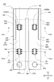
- FIG. 9 is an exploded perspective view for explaining the current sensor 102 according to the second embodiment of the present invention.
- FIG. 10 is a perspective view for explaining the current sensor 102 according to the second embodiment of the present invention.
- FIG. 11 is a configuration diagram for explaining the current sensor 102 according to the second embodiment of the present invention, and is a top view seen from the Z1 side shown in FIG.
- FIGS. 10 and 11 show the substrate 29 in a transparent state for ease of explanation.
- FIG. 12 is a configuration diagram for explaining the current sensor 102 according to the second embodiment of the present invention, and is a cross-sectional view taken along line XII-XII shown in FIG.
- the current sensor 102 of the second embodiment differs from the first embodiment in that the second current path 62 and the second magnetoelectric conversion element 63 are provided.
- the same composition as a 1st embodiment the same numerals are attached and detailed explanation is omitted.
- the current sensor 102 has a first current path 22 having a first flat portion 22f and a second current path having a second flat portion 62f, as shown in FIGS. 62, a connection portion 92 connecting one ends of the first current path 22 and the second current path 62, a first magnetoelectric conversion element 23 disposed on the first current path 22, and a second current path 62 And a second magnetoelectric conversion element 63 disposed on the upper side.
- a substrate 29 disposed opposite to the first current path 22 and the second current path 62, and although not shown, for supplying power to the current sensor 102 and for taking out a signal from the current sensor 102.
- a connector is provided in order to connect to an external control device.
- the first current path 22 is made of a metal material with good conductivity such as copper (Cu), and as shown in FIGS. 9 to 12, a first flat portion 22f and one of the first current paths 22.
- the first convex portion 22 w is provided with a first convex portion 22 w standing from the end portion 22 t, and the first convex portion 22 w is formed along the flow direction of the current to be measured (Y direction shown in FIG. 10) There is.
- a terminal portion 27A is provided on the other end side of the first current path 22 continuously to the first current path 22, and the terminal portion 27A is illustrated.
- a through hole 27h is provided for connecting and fixing the measured current path (current path to be measured) of a non-apparatus (device to be measured).
- the second current path 62 is made of a conductive metal material such as copper (Cu), and as shown in FIGS. 9 to 12, a second flat portion 62f and one of the second current paths 62.
- the second convex portion 62w is provided with a second convex portion 62w standing from the end portion 62t, and the second convex portion 62w is formed along the flow direction of the current to be measured (Y direction shown in FIG. 10). There is.
- a terminal portion 27B is provided continuously to the second current path 62 on the other end side of the second current path 62, and the terminal portion 27B is illustrated. There is provided a through hole 27k for connecting and fixing a current path to be measured (a current path to be measured) of a device (device to be measured).
- the first current path 22 and the second current path 62 are arranged in parallel, as shown in FIGS. 9 to 11, and one end of each is connected by a connection portion 92.
- the first convex portion 22 w of the first current path 22 is erected from the end 22 t on the side away from the second current path 62
- the second convex portion 62 w of the second current path 62 is the first It is disposed to stand from an end 22t remote from the current path 22.
- the 1st convex part 22w and the 2nd convex part 62w are arrange
- the first current path 22, the second current path 62, and the connection portion 92 are U-shaped, and the first current path 22 and the second current path 62 are It is line symmetrical.
- first flat portion 22f, the first convex portion 22w, the connection portion 92, the second flat portion 62f, and the second convex portion 62w described above integrally bend a metal plate such as copper (Cu). It is formed.
- a metal plate such as copper (Cu).
- the first magnetoelectric conversion element 23 is an element for detecting the magnetism generated when the current to be measured flows in the first current path 22.
- the first magnetoelectric conversion element 23 is a magnetoresistance effect element using a giant magnetoresistance effect (GMR (Giant It is packaged in the magnetic sensor package 24 as shown in FIG. 12 using a Magneto Resistive) element.
- GMR giant magnetoresistance effect
- the first magnetoelectric conversion element 23 is disposed on the first flat portion 22f of the portion where the first convex portion 22w is erected.
- the sensitivity direction of the first magnetoelectric transducer 23 is disposed in the X direction shown in FIG.
- the second magnetoelectric conversion element 63 is an element for detecting the magnetism generated when the current to be measured flows in the second current path 62 and, like the first magnetoelectric conversion element 23, for example, the giant magnetoresistance effect
- the magnetoresistive effect element (referred to as a GMR (Giant Magneto Resistive) element) used is packaged in a magnetic sensor package 64 as shown in FIG.
- the second magnetoelectric conversion element 63 is disposed on the second flat portion 62f of the portion where the second convex portion 62w is provided.
- the sensitivity direction of the second magnetoelectric transducer 63 is disposed in the X direction shown in FIG. Since differential processing is performed between the first magnetoelectric conversion element 23 and the second magnetoelectric conversion element 63, the sensitivity axes of the first magnetoelectric conversion element 23 and the second magnetoelectric conversion element 63 are in the same direction. It is arranged as
- the magnetic sensor package (24, 64) described above electrically connects the chip of the GMR element cut out to the lead terminal (24r, 64r) for signal extraction after the GMR element is fabricated on a silicon substrate It is manufactured by packaging with a thermosetting synthetic resin.
- the magnetic sensor package 24 and the magnetic sensor package 64 are provided on the same substrate 29 by being soldered to a substrate 29 which is a circuit substrate by lead terminals (24 r, 64 r).
- the magnetic sensor package 24 and the magnetic sensor package 64 are connected to an external control device via a wiring pattern and a connector (not shown).
- first magnetoelectric conversion element 23 and the second magnetoelectric conversion element 63 are packaged and disposed on the substrate 29 as the magnetic sensor package (24, 64), for example, the first magnetoelectric conversion element 23 and the second magnetoelectric conversion The element 63 may be disposed as it is, so-called bare chip mounting, and disposed on the same substrate 29.
- the substrate 29 uses a widely known double-sided printed wiring board, and a metal foil such as copper (Cu) provided on a base substrate is patterned on a glass-filled epoxy resin base substrate, A wiring pattern is formed.
- a metal foil such as copper (Cu) provided on a base substrate is patterned on a glass-filled epoxy resin base substrate, A wiring pattern is formed.
- one magnetic sensor package (4, 64) in which the first magnetoelectric conversion element 23 and the second magnetoelectric conversion element 63 are packaged is mounted on the substrate 29. It has become.
- a printed wiring board made of epoxy resin containing glass is used as the substrate 29, the present invention is not limited to this.
- a ceramic wiring board or a flexible wiring board may be used.
- a circuit board is preferably used as the board 29.
- the present invention is not limited to the circuit board, and the magnetic sensor package (24, 64) is obtained by superposing the circuit board on the board 29. May be mounted.
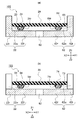
- FIG. 13 is a cross-sectional view of the first current path 22 and the second current path 62 of the model C1 used for the simulation of the current sensor of the second embodiment of the present invention.
- the numerical values used for this simulation set the entire length of the first current path 22 to 100 (mm), the entire width W21 to 20 (mm), and the thickness T21 of the first flat portion 22f.
- the length of the first convex portion 22w is 60 (mm), the width W22 is 4 (mm), and the height T22 is 10 (mm).
- the overall length of the second current path 62 is 100 (mm), the overall width W 61 is 20 (mm), and the thickness T 61 of the second flat portion 62 f is 4 (mm).
- the length was 60 (mm), the width W 62 was 4 (mm), and the height T 62 was 10 (mm).
- the distance W41 between the first current path 22 and the second current path 62 is 5 (mm).
- the magnetic flux density in a space 1 mm away from the surface of the first current path 22 and the second current path 62 was used.
- the current sensor 102 shown in FIGS. 9 to 12 is an embodiment of the model C1.
- FIG. 14 is a simulation result of the model C1 of the current sensor of the second embodiment of the present invention.
- the horizontal axis of the graph in FIG. 14 indicates the distance in the width direction when the midpoint between the first current path 22 and the second current path 62 is zero, and the negative side is the first current path 22 and the positive side is the second. It is the current path 62.
- the vertical axis of the graph of FIG. 14 indicates the magnetic flux density in a portion where the first convex portion 22 w of the first flat portion 22 f and the second convex portion 62 w of the second flat portion 62 f are not provided.
- P21 in the figure indicates the lowest frequency magnetic flux density when the frequency of the current to be measured used in the device (device to be measured) is 10 (Hz) and the lowest frequency assumed
- P22 in the figure is The frequency of the measured current used in the device (device to be measured) is 10 (kHz), which indicates the highest frequency magnetic flux density in the case of the highest frequency assumed.
- the low frequency and the high frequency of the current to be measured are on the second flat portion 62f where the second convex portion 62w is not provided.
- the difference in magnetic flux density due to the difference between the two that is, the difference between the lowest frequency magnetic flux density P21 and the highest frequency magnetic flux density P22 is small. It is considered that this is because the magnetic field around the second current path 62 was changed by providing the second convex portion 62 w. Therefore, the lowest frequency magnetic flux density P21 and the highest frequency magnetic flux density P22 can be made closer to each other by providing the conductive second convex portion 62w along the flowing direction of the current to be measured, and can be made to more coincide with each other.
- the first magnetoelectric conversion element 23 and the second magnetoelectric conversion element are provided at positions above the first current path 22 and the second current path 62 where the lowest frequency magnetic flux density P21 and the highest frequency magnetic flux density P22 substantially match.
- 63 are provided.
- the distance from the center is about ⁇ 7.5 (on the first flat portion 22f where the first convex portion 22w of the first current path 22 is not provided).
- the first magnetoelectric conversion element 23 It is desirable to dispose the first magnetoelectric conversion element 23 at a position of about 5 (mm) from the other end of the first current path 22, and the second convex portion 62 w of the second current path 62 is provided The second magnetoelectric conversion element at a distance of about 7.5 (mm) ⁇ about 5 (mm) from the other end of the second current path 62 ⁇ on the second flat portion 62f which is not It is desirable to arrange 63.
- the first magnetoelectric conversion element 23 and the second magnetoelectric conversion element 63 can be disposed at a position where the change in magnetic flux density due to the frequency change is small. Since the lowest frequency magnetic flux density P ⁇ b> 21 and the highest frequency magnetic flux density P ⁇ b> 22 do not greatly differ even if the frequency of [1] changes, the current value can be measured accurately.
- the first magnetoelectric conversion element 23 and the second magnetoelectric conversion element 63 are provided on the same substrate 29 respectively, the current in the external magnetic field or the current path (the first current path 22 and the second current path 62) The influence by the internal magnetic field generated when the magnetic flux flows appears with the same strength in the two magnetoelectric conversion elements (the first magnetoelectric conversion element 23 and the second magnetoelectric conversion element 63). Therefore, by differentially processing the outputs from the two magnetoelectric conversion elements (the first magnetoelectric conversion element 23 and the second magnetoelectric conversion element 63), the influence of the magnetic field can be offset more accurately. By this, the deterioration of the measurement accuracy of the current sensor 102 can be reduced.
- the position where the change of the magnetic flux density accompanying the frequency change is small It can be changed arbitrarily.
- positioning position of the 1st desired magnetoelectric conversion element 23 can also be set arbitrarily.
- the position at which the change in the magnetic flux density accompanying the change in the frequency is small can be arbitrarily changed by changing the shape of the first convex portion 22w, for example, the length or the surface shape of the corner. .
- the first magnetoelectric conversion element 23 be disposed at a position on the first current path 22 where the lowest frequency magnetic flux density P21 and the highest frequency magnetic flux density P22 substantially match, the lowest frequency magnetic flux density
- the first magnetoelectric conversion element 23 may be disposed at a position on the first current path 22 corresponding to a region where P21 and the maximum frequency magnetic flux density P22 become equal.
- a region where the lowest frequency magnetic flux density P21 and the highest frequency magnetic flux density P22 are equal ie, the distance from the center is -6 (mm)
- the first magnetoelectric conversion element 23 may be disposed between 14 (mm), preferably between -7 (mm) and -9 (mm).
- the distance from the center is between 6 (mm) and 14 (mm), preferably between 7 (mm) and 9 (mm)
- the second magnetoelectric conversion element 63 may be disposed.
- the first convex portion 22 w and the second convex portion 62 w can be provided so that the region where the lowest frequency magnetic flux density P 21 and the highest frequency magnetic flux density P 22 are equal is wide.
- the first magnetoelectric conversion element 23 and the second magnetoelectric conversion element 63 can be disposed arbitrarily within the range of this region, for example, when the position where the current sensor 102 can be disposed is limited in an on-vehicle application Even if it is, the 1st magnetoelectric conversion element 23 and the 2nd magnetoelectric conversion element 63 can be arranged in the best position.
- the first current path 22 is provided with the conductive first convex portion 22 w which is long along the flowing direction of the current to be measured.
- the lowest frequency magnetic flux density P21 which is the magnetic flux density when the measured current of the lowest frequency used in the instrument
- the highest frequency magnetic flux density P22 which is the magnetic flux density when the measured current of the highest frequency flows. It can be closely matched more closely. Therefore, the first magnetoelectric conversion element 23 can be disposed at a position where the change in magnetic flux density due to the change in frequency is small. As a result, even if the frequency of the current to be measured changes, the lowest frequency magnetic flux density P21 and the highest frequency magnetic flux density P22 do not greatly differ, so that the current value can be measured accurately.
- the second current path 62 is provided with the conductive second convex portion 62w along the flowing direction of the current to be measured, the magnetic flux in the case of flowing the current to be measured of the lowest frequency used in the device.
- the lowest frequency magnetic flux density P21 which is the density
- the highest frequency magnetic flux density P22 which is the magnetic flux density in the case where the current to be measured at the highest frequency is supplied, can be made closer to each other.
- the second magnetoelectric conversion element 63 can be disposed at a position where the change in magnetic flux density due to the change in frequency is small.
- the lowest frequency magnetic flux density P21 and the highest frequency magnetic flux density P22 do not greatly differ, so that the current value can be measured accurately also in the second current path 62.
- the first magnetoelectric conversion element 23 and the second magnetoelectric conversion element 63 are provided on the same substrate 29 respectively, the current in the external magnetic field or the current path (the first current path 22 and the second current path 62) The influence by the internal magnetic field generated when the magnetic flux flows appears with the same strength in the two magnetoelectric conversion elements (the first magnetoelectric conversion element 23 and the second magnetoelectric conversion element 63). Therefore, by differentially processing the outputs from the two magnetoelectric conversion elements (the first magnetoelectric conversion element 23 and the second magnetoelectric conversion element 63), the influence of the magnetic field can be offset more accurately. By this, the deterioration of the measurement accuracy of the current sensor 102 can be reduced.
- first flat portion 22f, the first convex portion 22w, the connection portion 92, the second flat portion 62f, and the second convex portion 62w are integrally formed by bending a metal plate such as copper (Cu).
- a metal plate such as copper (Cu).
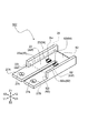
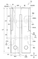
- FIG. 15 is an exploded perspective view for explaining the current sensor 103 according to the third embodiment of the present invention.
- FIG. 16 is a perspective view for explaining the current sensor 103 according to the third embodiment of the present invention.
- FIG. 17 is a configuration diagram for explaining the current sensor 103 according to the third embodiment of the present invention, and is a top view seen from the Z1 side shown in FIG.
- FIGS. 16 and 17 show the substrate 29 in a transparent state for ease of explanation.
- FIG. 18 is a configuration diagram for explaining a current sensor 103 according to a third embodiment of the present invention, and FIG. 18 (a) is a cross-sectional view along line XVII-XVII shown in FIG.
- the current sensor 103 according to the third embodiment is different from the second embodiment in that the first magnetoelectric conversion element 33 and the second magnetoelectric conversion element 73 are provided.
- the same composition as a 1st embodiment and a 2nd embodiment the same numerals are attached and detailed explanation is omitted.
- the current sensor 103 has a first current path 22 having a first flat portion 22f and a second current path having a second flat portion 62f, as shown in FIGS. 62, a connection portion 92 connecting one ends of the first current path 22 and the second current path 62, and a first magnetoelectric conversion element 23 and a first magnetoelectric conversion element 33 disposed on the first current path 22. , And a second magnetoelectric conversion element 63 and a second magnetoelectric conversion element 73 disposed on the second current path 62.
- the substrate 29 disposed opposite to the first current path 22 and the second current path 62, and although not shown, for supplying power to the current sensor 103 and for taking out a signal from the current sensor 103.
- a connector is provided in order to connect to an external control device.
- the first current path 22, the second current path 62, and the connection portion 92 have the same structure as in the second embodiment, and thus the description thereof will be omitted.
- the first magnetoelectric conversion element 23 is disposed on the first position 22a of the first flat portion 22f on which the first convex portion 22w is provided.
- the sensitivity direction of the first magnetoelectric transducer 23 is disposed in the X direction shown in FIG.
- the first magnetoelectric conversion element 33 is an element for detecting the magnetism generated when the current to be measured flows in the first current path 22.
- the first magnetoelectric conversion element 33 is a magnetoresistance effect element using a giant magnetoresistance effect (GMR (Giant It is packaged in a magnetic sensor package 34 as shown in FIG. 18 using a Magneto Resistive) element.
- GMR giant magnetoresistance effect
- the first magnetoelectric conversion element 33 is disposed on the third position 22c of the first flat portion 22f in which the first convex portion 22w is not provided.
- the sensitivity direction of the first magnetoelectric conversion element 33 is disposed so as to be the X direction shown in FIG. 17 so that the same sensitivity axis as the first magnetoelectric conversion element 23 is directed.
- the second magnetoelectric conversion element 63 is disposed on the second position 62b of the second flat portion 62f on which the second convex portion 62w is provided.
- the sensitivity direction of the second magnetoelectric transducer 63 is disposed in the X direction shown in FIG.
- the second magnetoelectric conversion element 73 is an element for detecting the magnetism generated when the current to be measured flows in the second current path 62, and, for example, a magnetoresistance effect element (GMR (Giant) using a giant magnetoresistance effect. It is packaged in a magnetic sensor package 74 as shown in FIG. In addition, as shown in FIGS. 16 and 17, the second magnetoelectric conversion element 73 is disposed on the fourth position 62d of the second flat portion 62f where the second convex portion 62w is not provided. The sensitivity direction of the second magnetoelectric conversion element 73 is disposed so as to be the X direction shown in FIG. 17 so that the same sensitivity axis as the second magnetoelectric conversion element 63 is directed.
- GMR magnetoresistance effect element
- the above-mentioned magnetic sensor package (24, 34, 64, 74) has a GMR element fabricated on a silicon substrate, and then the chip of the GMR element cut out and lead terminals (24r, 34r, 64r, 74r) are electrically connected and packaged by a thermosetting synthetic resin. And this magnetic sensor package (24, 34, 64, 74) is soldered to the board 29 which is a circuit board by lead terminals (24r, 34r, 64r, 74r), and provided on the same board 29 There is.
- the magnetic sensor package (24, 34, 64, 74) is connected to an external control device via a wiring pattern and a connector (not shown).
- magnetic field analysis was performed using a finite element analysis system regarding changes in the magnetic field when measured currents having different frequencies flow.
- FIG. 19 is a plan view of the first current path 22, the second current path 62, and the connection portion 92 of the model D1 used for the simulation of the current sensor of the third embodiment of the present invention.
- FIG. 20 is a cross-sectional view of the first current path 22 and the second current path 62 of the model D1 used for the simulation of the current sensor of the third embodiment of the present invention, and a cross section along line XVII-XVII shown in FIG.
- FIG. FIG. 21 shows a simulation result of the current sensor according to the third embodiment of the present invention, which is a simulation result in the XVII-XVII line direction shown in FIG. 22 shows simulation results, and FIG. 22 (a) shows simulation results in the direction of XX-XX line shown in FIG.
- the comparative example H131 is a model without the first convex portion 22w and the second convex portion 62w shown in FIG.
- P31 in the figure indicates the lowest frequency magnetic flux density when the frequency of the measured current used in the device (device to be measured) is 10 (Hz) and the lowest frequency assumed
- P32 in the figure is The frequency of the measured current used in the device (device to be measured) is 10 (kHz), which indicates the highest frequency magnetic flux density in the case of the highest frequency assumed.
- the numerical values used for this simulation set the entire length L21 of the first current path 22 to 120 (mm), the entire width W 21 to 20 (mm), and the first flat portion
- the thickness T21 of 22f is 4 (mm)
- the length L22 of the first convex portion 22w is 60 (mm)
- the width W22 is 4 (mm)
- the height T22 is 4 (mm).
- the entire length of the second current path 62 is also 100 (mm)
- the entire width W 61 is 20 (mm)
- the thickness T 61 of the second flat portion 62 f is 4 (mm).
- the length was also 60 (mm), the width W 62 was 4 (mm), and the height T 62 was 4 (mm).
- the length L53 from the end of the first current path 22 and the second current path 62 to the XVII-XVII line is 30 (mm), and the end of the first convex portion 22w and the second convex portion 62w is XVIII.
- the length L63 to the -XVIII line is set to 20 (mm). That is, the length between the XVII-XVII line and the XVIII-XVIII line is 40 (mm).
- the length W81 from the middle point of the first current path 22 and the second current path 62 to the XX-X line is 12.5 (mm).
- the distance W41 between the first current path 22 and the second current path 62 is 5 (mm).
- the magnetic flux density in a space 1 mm away from the surface of the first current path 22 and the second current path 62 was used.
- the current sensor 103 shown in FIGS. 15 to 18 is an embodiment of the model D1.
- the low frequency and high frequency of the current to be measured are on the second flat portion 62f where the second convex portion 62w is not provided.
- the difference between the magnetic flux density due to the difference between the lower frequency magnetic flux density P31 and the highest frequency magnetic flux density P32 is smaller. It is considered that this is because the magnetic field around the second current path 62 was changed by providing the second convex portion 62 w. Therefore, the lowest frequency magnetic flux density P31 and the highest frequency magnetic flux density P32 can be made closer to each other by providing the conductive second convex portion 62w along the direction in which the current to be measured flows, and can be made more consistent.
- the first magnetoelectric conversion element 23 and the second magnetoelectric conversion element are disposed at positions above the first current path 22 and the second current path 62 where the lowest frequency magnetic flux density P31 and the highest frequency magnetic flux density P32 substantially match.
- 63 are provided.
- the distance from the center is about ⁇ 7.5 (on the first flat portion 22f where the first convex portion 22w of the first current path 22 is not provided).
- the first magnetoelectric conversion element 23 It is desirable to dispose the first magnetoelectric conversion element 23 at a position of about 5 (mm) from the other end of the first current path 22, and the second convex portion 62 w of the second current path 62 is provided The second magnetoelectric conversion element at a distance of about 7.5 (mm) ⁇ about 5 (mm) from the other end of the second current path 62 ⁇ on the second flat portion 62f which is not It is desirable to arrange 63.
- the first magnetoelectric conversion element 23 and the second magnetoelectric conversion element 63 can be disposed at a position where the change in magnetic flux density due to the frequency change is small. Since the lowest frequency magnetic flux density P ⁇ b> 31 and the highest frequency magnetic flux density P ⁇ b> 32 do not greatly differ even if the frequency of [1] changes, the current value can be measured accurately.
- the first magnetoelectric conversion element 23 and the second magnetoelectric conversion element 63 are provided on the same substrate 29 respectively, the current in the external magnetic field or the current path (the first current path 22 and the second current path 62) The influence by the internal magnetic field generated when the magnetic flux flows appears with the same strength in the two magnetoelectric conversion elements (the first magnetoelectric conversion element 23 and the second magnetoelectric conversion element 63). Therefore, by differentially processing the outputs from the two magnetoelectric conversion elements (the first magnetoelectric conversion element 23 and the second magnetoelectric conversion element 63), the influence of the magnetic field can be offset more accurately. By this, the deterioration of the measurement accuracy of the current sensor 102 can be reduced.
- both the lowest frequency magnetic flux density P31 and the highest frequency magnetic flux density P32 are based on the magnetic flux density of the portion (40 (mm) in the figure) of line XVIII-XVIII.
- the magnetic flux density of the part (0 (mm) in the figure) is smaller. That is, the magnetic flux density of the portion of the XVII-XVII line at the first position 22a where the first convex portion 22w is erected and the magnetic flux density of the portion of the XVIII-XVIII line at the third position 22c where the first convex portion 22w is not erected Are very different.
- both the lowest frequency magnetic flux density P31 and the highest frequency magnetic flux density P32 have the magnetic flux density of a portion (40 (mm) in the figure) of the XVIII-XVIII line.
- the magnetic flux density in the portion of the XVII-XVII line (0 (mm) in the figure) is almost the same.
- the first magnetoelectric conversion element 23 is disposed on the first position 22a of the first current path 22 where the first convex portion 22w is erected, and the first current path 22 where the first convex portion 22w is not erected.
- the first magnetoelectric conversion element 33 By arranging the first magnetoelectric conversion element 33 on the third position 22c, the absolute amount of the magnetic quantity detected by the first magnetoelectric conversion element 33 differs from the magnetic quantity detected by the first magnetoelectric conversion element 33. . Therefore, the first magnetoelectric conversion element 23 disposed at the first position 22a can be used separately for high current measurement and the first magnetoelectric conversion element 33 disposed at the third position 22c for constant current measurement. .
- the disposition position of the first magnetoelectric conversion element 23 is the first position 22a. mm) ⁇ 5 mm from the end of the first convex portion ⁇ to +5 (mm) is preferable, and the disposition position of the first magnetoelectric conversion element 33 is the third position 22c, which is -35 A region separated by (mm) ⁇ 15 (mm) or more from the end of the first convex portion ⁇ is preferable.
- the amount of magnetism detected by the second magnetoelectric conversion element 63 and the absolute amount of magnetism detected by the second magnetoelectric conversion element 73 differ, so the second magnetoelectric conversion element 63 disposed at the second position 62b
- the second magnetoelectric conversion element 73 disposed at the fourth position 62d can be used separately for high current measurement and low current measurement.
- measurement can be performed in a wide range, and in the case of low current measurement, measurement can be performed with high accuracy.
- the first magnetoelectric conversion element 33 and the second magnetoelectric conversion element 73 are provided on the same substrate 29 respectively, the current in the external magnetic field or the current path (the first current path 22 and the second current path 62)
- the influence of the internal magnetic field generated when the magnetic flux flows appears in the two magnetoelectric conversion elements (the first magnetoelectric conversion element 33 and the second magnetoelectric conversion element 73) with the same strength. Therefore, by differentially processing the outputs from the two magnetoelectric conversion elements (the first magnetoelectric conversion element 33 and the second magnetoelectric conversion element 73), the influence of the magnetic field can be canceled more accurately. As a result, the deterioration of the measurement accuracy of the current sensor 103 can be reduced.
- the first current path 22 is provided with the conductive first convex portion 22 w which is long along the flowing direction of the current to be measured, Equipment) the lowest frequency magnetic flux density P31, which is the magnetic flux density in the case of flowing the measured current of the lowest frequency used in the device), and the highest frequency magnetic flux density P32, which is the magnetic flux density in the case of flowing the measured current of the highest frequency It can be closely matched more closely. Therefore, the first magnetoelectric conversion element 23 can be disposed at a position where the change in magnetic flux density due to the change in frequency is small. As a result, even if the frequency of the current to be measured changes, the lowest frequency magnetic flux density P31 and the highest frequency magnetic flux density P32 do not greatly differ, so that the current value can be measured accurately.
- the second current path 62 is provided with the conductive second convex portion 62w along the flowing direction of the current to be measured, the magnetic flux in the case of flowing the current to be measured of the lowest frequency used in the device.
- the lowest frequency magnetic flux density P31 which is the density
- the highest frequency magnetic flux density P32 which is the magnetic flux density in the case where the current to be measured at the highest frequency flows, can be brought closer to each other to be more consistent.
- the second magnetoelectric conversion element 63 can be disposed at a position where the change in magnetic flux density due to the change in frequency is small. As a result, even if the frequency of the current to be measured changes, the lowest frequency magnetic flux density P31 and the highest frequency magnetic flux density P32 do not greatly differ, so that the current value can be measured accurately also in the second current path 62. .
- the first magnetoelectric conversion element 23 and the second magnetoelectric conversion element 63 are provided on the same substrate 29 respectively, the current in the external magnetic field or the current path (the first current path 22 and the second current path 62) The influence by the internal magnetic field generated when the magnetic flux flows appears with the same strength in the two magnetoelectric conversion elements (the first magnetoelectric conversion element 23 and the second magnetoelectric conversion element 63). Therefore, by differentially processing the outputs from the two magnetoelectric conversion elements (the first magnetoelectric conversion element 23 and the second magnetoelectric conversion element 63), the influence of the magnetic field can be offset more accurately. By this, the deterioration of the measurement accuracy of the current sensor 102 can be reduced.
- the first magnetoelectric conversion element 33 and the second magnetoelectric conversion element 73 disposed at the position 62d are separately disposed.
- the magnetic amount detected by the first magnetoelectric conversion element 23 and the second magnetoelectric conversion element 63 disposed at the first position 22a and the second position 62b, and the third position 22c and the fourth position 62d are provided.
- the absolute amount of the amount of magnetism detected by the first magnetoelectric conversion element 33 and the second magnetoelectric conversion element 73 differs. Therefore, the first magnetoelectric conversion element 23 and the second magnetoelectric conversion element 63 disposed at the first position 22a and the second position 62b are disposed at the third position 22c and the fourth position 62d for high current measurement.
- the first magnetoelectric conversion element 33 and the second magnetoelectric conversion element 73 can be selectively used for constant current measurement. As a result, in the case of high current measurement, measurement can be performed in a wide range, and in the case of low current measurement, measurement can be performed with high accuracy.
- FIG. 23 is a view for explaining a modification of the current sensor 101 according to the first embodiment of the present invention, and FIG. 23 (a) is a model AC1 of the modification 1, and FIG. 23 (b) is a modification FIG. 23 (c) is a model AC3 of the third modification, and FIG. 23 (d) is a model AC4 of the fourth modification.
- FIG. 24 is a view for explaining a modification of the current sensor 101 according to the first embodiment of the present invention, and FIG. 24 (a) is a plan view of a current sensor C105 according to a modification 5; ) Is a plan view of a current sensor C106 of the sixth modification.
- FIG. 24 is a view for explaining a modification of the current sensor 101 according to the first embodiment of the present invention, and FIG. 24 (a) is a plan view of a current sensor C105 according to a modification 5; ) Is a plan view of a current sensor C106 of the sixth modification.
- FIG. 24 is a view for explaining a modification
- FIG. 25 is a view for explaining a modification of the current sensor 102 according to the second embodiment of the present invention
- FIG. 25 (a) is a perspective view of the current sensor C107 according to the seventh modification.
- b) is a perspective view of current sensor C108 of modification 8
- Drawing 25 (c) is a perspective view of current sensor C109 of modification 9.
- the first convex portion 12w is erected from the end 12t of the first flat portion 12f, and the end face of the first flat portion 12f is flush with one surface of the first convex portion 12w.
- the first flat portion 12f is formed so that the end face of the first flat portion 12f and one surface of the first convex portion 12w are not flush.
- the first convex portion C12w may be erected from the end portion 12t of the lens.
- the structure of 1st convex part C22w which does not stand from the edge part 12t of the 1st flat-shaped part 12f may be sufficient.
- the cross-sectional shape of the first convex portion 12 w is configured to be rectangular, but the shape is not limited to rectangular and may be configured to be other shape.
- it may be a trapezoidal first convex portion C32w, or as shown in FIG. 23 (d), it may be a first convex portion C42w having a stepped portion. It may be formed, or may be formed in a step-like manner.
- the first convex portion 12w is provided over the entire length in the longitudinal direction of the first current path 12. However, as shown in FIG. 24 (a), the first convex is formed in part of the longitudinal direction. A portion C52w may be provided, or as shown in FIG. 24 (b), a first convex portion C62w in which the end face of the first flat portion 12f and one surface of the first convex portion 12w are not flush. May be provided.
- the first convex portion 22w of the first current path 22 and the second convex portion 62w of the second current path 62 are configured to face each other at the same size and at the same position. For example, as shown to Fig.25 (a), you may make it the structure mutually shifted and opposed.
- the first convex portion 22 w of the first current path 22 and the second convex portion 62 w of the second current path 62 extend to the end portions in the longitudinal direction of the first current path 22 and the second current path 62.
- the present invention is not limited to this.
- the first convex portion 22w may be provided so as not to extend to the end (C72a, C72b) in the longitudinal direction.
- the first current path A configuration may be provided in which wall portions 82 w erected from the end portions (C 72 a, C 72 b) in the longitudinal direction of the second current path 62 and the second current path 62 and the end portion C 92 t of the connection portion 92 are provided.
- GMR elements are suitably used as the first magnetoelectric conversion element (13, 23, 33) and the second magnetoelectric conversion element (163, 7), but any magnetic detection element capable of detecting magnetism may be used.
- the present invention is not limited to the above embodiment, and can be appropriately modified without departing from the scope of the object of the present invention.
Abstract
【課題】被測定電流の周波数が変化しても精度良く測定ができる電流センサを提供することを目的とする。 【解決手段】電流センサ101は、第1扁平形状部12fを有する第1電流路12と、第1電流路12上に配設され第1電流路12に被測定電流が流れたときに発生する磁気を検出する第1磁電変換素子13と、を備え、第1電流路12が接続される機器の被測定電流を測定し、第1電流路12には、被測定電流の流れる方向に沿って導電性の第1凸部12wが設けられており、機器で用いられる最低周波数の被測定電流を流した場合における磁束密度である最低周波数磁束密度と、機器で用いられる最高周波数の被測定電流を流した場合における磁束密度である最高周波数磁束密度と、が、略一致する第1電流路12上の位置に、第1磁電変換素子13が配設されることを特徴としている。
Description
本発明は、各種機器に流れる被測定電流を磁電変換素子によって測定する電流センサに関し、特に、インバータ等が搭載された各種機器に流れる被測定電流の周波数が変化する場合に適した電流センサに関する。
近年、各種機器の制御や監視のために、各種機器に取り付けて各種機器に流れる被測定電流を測定する電流センサが一般に用いられている。この種の電流センサとして、電流路に流れる被測定電流から生じる磁界を検知する、磁気抵抗効果素子やホール素子等の磁電変換素子(磁気検出素子)を用いた方法が良く知られている。
上述した電流センサの内で、扁平な形状の被測定導体(電流路)と絶縁基板上に配設された磁気センサとを用いた、特許文献1に提案されているような電流測定装置(電流センサ)900が一般的に知られている。図27は、特許文献1に開示されている電流測定装置900を説明する図であって、磁気センサ910と被測定導体901との位置関係を示す断面図である。電流測定装置900は、図27に示すように、プリント基板911に形成された被測定導体901と、プリント基板912に搭載された磁気センサ910(内部に磁気検出素子を備えている)とから構成されており、被測定導体901に被測定電流が流れた際に、被測定導体901幅方向に生じる磁界920を磁気センサ910で検出している。
ところで、このような扁平な形状の被測定導体901中を流れる被測定電流の周波数が高くなると、表皮効果により、被測定電流が被測定導体901の端部に集中し、被測定導体901の中央では電流密度が小さくなり、被測定導体901の端付近では電流密度が大きくなる。このため、磁気センサ910を被測定導体901の中央に配置した場合(図27では端部に配置)、磁気センサ910が検知する中央付近の磁界920が低下し、電流測定装置900の電流感度が下がると言う問題があった。
そこで、従来例の電流測定装置900では、図27に示すように、被測定導体901の幅方向の中央位置CLから所定距離だけ離れた位置に磁気センサ910を設けるようにしている。これにより、周波数が高い被測定電流であっても、測定感度の低下が抑えられた電流測定装置900を提供できるとしている。
しかしながら、従来例では、測定する被測定電流の周波数に合わせて磁気センサ910を被測定導体901の端付近に配置するので、周波数の違う被測定電流を用いた他の機器に適用する場合や同じ機器であっても周波数が状態によって変化する場合、電流測定装置900で測定する電流感度が大きく違い、正確な測定精度が得られないと言う課題があった。なお、状態によって被測定電流の周波数が変化する場合とは、例えば、電気自動車やハイブリッド自動車において、アイドリング時、加速時、回生ブレーキ時等の状態によって、被測定電流の周波数が変化する場合が挙げられる。
本発明は、上述した課題を解決するもので、被測定電流の周波数が変化しても精度良く測定ができる電流センサを提供することを目的とする。
この課題を解決するために、本発明の電流センサは、第1扁平形状部を有する第1電流路と、前記第1電流路上に配設され前記第1電流路に被測定電流が流れたときに発生する磁気を検出する第1磁電変換素子と、を備え、前記第1電流路が接続される機器の前記被測定電流を測定する電流センサにおいて、前記第1電流路には、前記被測定電流の流れる方向に沿って導電性の第1凸部が設けられており、前記機器で用いられる最低周波数の前記被測定電流を流した場合における磁束密度である最低周波数磁束密度と、前記機器で用いられる最高周波数の前記被測定電流を流した場合における磁束密度である最高周波数磁束密度と、が略一致する前記第1電流路上の位置に、前記第1磁電変換素子が配設されることを特徴としている。
これによれば、本発明の電流センサは、第1電流路には、被測定電流の流れる向きに沿って導電性の第1凸部が設けられているので、機器で用いられる最低周波数の被測定電流を流した場合における磁束密度である最低周波数磁束密度と、最高周波数の被測定電流を流した場合における磁束密度である最高周波数磁束密度と、を近づけてより一致させることができる。このため、周波数変化に伴う磁束密度の変化が小さい位置に、第1磁電変換素子を配設することができる。このことにより、被測定電流の周波数が変化しても最低周波数磁束密度と最高周波数磁束密度とが大きく異ならないので、精度良く電流値を測定することができる。
また、本発明の電流センサは、前記第1凸部は、前記第1扁平形状部のいずれか一方の端部から立設していることを特徴としている。
これによれば、最低周波数磁束密度と最高周波数磁束密度とが略一致する位置を、第1電流路の中央側に移動させることができる。このことにより、第1磁電変換素子を第1電流路の中央付近により近づけて配設でき、従来例のように被測定導体(電流路)901の外側に磁気センサ(磁電変換素子)910を配置した場合と比較して、隣り合う電流路等からの外部磁場の影響を低減することができる。
また、本発明の電流センサは、前記第1扁平形状部及び前記第1凸部は、金属板を折り曲げて、一体で形成されていることを特徴としている。
これによれば、第1扁平形状部と第1凸部とを製造する際に、1枚の金属板から容易に製造することができる。このことにより、電流センサを安価にすることができる。
また、本発明の電流センサは、第2扁平形状部を有する第2電流路と、前記第2電流路上に配設され前記第2電流路に前記被測定電流が流れたときに発生する磁気を検出する第2磁電変換素子と、を備え、前記第1電流路と前記第2電流路との一端同士を接続する接続部が設けられ、前記第1電流路と前記第2電流路とは並列に配置され、前記第2電流路の他端が前記機器に接続され、前記第2電流路には、前記被測定電流の流れる方向に沿って導電性の第2凸部が設けられており、前記機器で用いられる最低周波数の前記被測定電流を流した場合における磁束密度である最低周波数磁束密度と、前記機器で用いられる最高周波数の前記被測定電流を流した場合における磁束密度である最高周波数磁束密度と、が略一致する前記第2電流路上の位置に、前記第2磁電変換素子が配設され、前記第1凸部が、前記第2電流路から離れた側の端部から立設しており、前記第2凸部が、前記第1電流路から離れた側の端部から立設しており、前記第1磁電変換素子と前記第2磁電変換素子とは、同一基板上に設けられていることを特徴としている。
これによれば、第2電流路には、被測定電流の流れる向きに沿って導電性の第2凸部が設けられているので、機器で用いられる最低周波数の被測定電流を流した場合における磁束密度である最低周波数磁束密度と、最高周波数の被測定電流を流した場合における磁束密度である最高周波数磁束密度と、を近づけてより一致させることができる。このため、周波数変化に伴う磁束密度の変化が小さい位置に、第2磁電変換素子を配設することができる。このことにより、被測定電流の周波数が変化しても最低周波数磁束密度と最高周波数磁束密度とが大きく異ならないので、第2電流路においても、精度良く電流値を測定することができる。更に、第1磁電変換素子と第2磁電変換素子を用い、それぞれ同一基板上に設けるようにしたので、外部磁界や電流路(第1電流路及び第2電流路)に電流が流れたときに発生する内部磁界による影響が、2つの磁電変換素子(第1磁電変換素子及び第2磁電変換素子)に同じ強さで現れてくる。このため、2つの磁電変換素子(第1磁電変換素子及び第2磁電変換素子)からの出力を差動処理することにより、この磁界の影響をより正確に相殺することができる。このことにより、電流センサの測定精度の悪化を低減することができる。
また、本発明の電流センサは、前記第1磁電変換素子を少なくとも2つ以上有するとともに、前記第2磁電変換素子を少なくとも2つ以上有し、前記第1磁電変換素子の少なくとも1つが、前記第1凸部が立設された前記第1扁平形状部の第1位置に配設されるとともに、前記第1磁電変換素子の少なくとも1つが、前記第1凸部が立設されない前記第1扁平形状部の第3位置に配設され、前記第2磁電変換素子の少なくとも1つが、前記第2凸部が立設された前記第2扁平形状部の第2位置に配設されるとともに、前記第2磁電変換素子の少なくとも1つが、前記第2凸部が立設されない前記第2扁平形状部の第4位置に配設されることを特徴としている。
これによれば、第1凸部が立説された第1電流路の第1位置及び第2凸部が立説された第2電流路の第2位置に配設される第1磁電変換素子及び第2磁電変換素子と、第1凸部が立説されない第1電流路の第3位置及び第2凸部が立説されない第2電流路の第4位置に配設される第1磁電変換素子及び第2磁電変換素子と、を、それぞれ分けて配設している。これにより、第1位置及び第2位置に配設された第1磁電変換素子及び第2磁電変換素子が検出する磁気量と、第3位置及び第4位置に配設された第1磁電変換素子及び第2磁電変換素子が検出する磁気量の絶対量が違ってくる。このため、第1位置及び第2位置に配設される第1磁電変換素子及び第2磁電変換素子を高電流測定用、第3位置及び第4位置に配設される第1磁電変換素子及び第2磁電変換素子を定電流測定用と、使い分けることができる。このことにより、高電流測定用では、ワイドレンジで測定することができ、低電流測定用では、精度良く測定することができる。
また、本発明の電流センサは、前記第1扁平形状部、前記第1凸部、前記接続部、前記第2扁平形状部及び前記第2凸部が、金属板を折り曲げて、一体で形成されていることを特徴としている。
これによれば、第1扁平形状部と第1凸部と接続部と第2扁平形状部と第2凸部とを製造する際に、1枚の金属板から容易に製造することができる。このことにより、電流センサを安価にすることができる。
本発明の電流センサは、第1電流路には、被測定電流の流れる向きに沿って長い導電性の第1凸部が設けられているので、機器(被測定機器)で用いられる最低周波数の被測定電流を流した場合における磁束密度である最低周波数磁束密度と、最高周波数の被測定電流を流した場合における磁束密度である最高周波数磁束密度と、を近づけてより一致させることができる。このため、周波数変化に伴う磁束密度の変化が小さい位置に、第1磁電変換素子を配設することができる。このことにより、被測定電流の周波数が変化しても最低周波数磁束密度と最高周波数磁束密度とが大きく異ならないので、精度良く電流値を測定することができる。
以下、本発明の実施の形態について図面を参照して説明する。
[第1実施形態]
図1は、本発明の第1実施形態の電流センサ101を説明する分解斜視図である。図2は、本発明の第1実施形態の電流センサ101を説明する斜視図である。なお、説明を容易にするため、絶縁基板19を省略している。図3は、本発明の第1実施形態の電流センサ101を説明する構成図であって、図2に示すZ1側から見た上面図である。図4は、本発明の第1実施形態の電流センサ101を説明する構成図であって、図3に示すIV-IV線における断面図である。
図1は、本発明の第1実施形態の電流センサ101を説明する分解斜視図である。図2は、本発明の第1実施形態の電流センサ101を説明する斜視図である。なお、説明を容易にするため、絶縁基板19を省略している。図3は、本発明の第1実施形態の電流センサ101を説明する構成図であって、図2に示すZ1側から見た上面図である。図4は、本発明の第1実施形態の電流センサ101を説明する構成図であって、図3に示すIV-IV線における断面図である。
本発明の第1実施形態の電流センサ101は、図1ないし図4に示すように、第1扁平形状部12fを有する第1電流路12と、第1電流路12上に配設される第1磁電変換素子13と、を備えて構成されている。他に、第1電流路12と対向して配設された絶縁基板19や、図示はしていないが、電流センサ101への電力の供給や電流センサ101からの信号取り出しのために、外部制御機器と接続するコネクタが備えられている。
第1電流路12は、銅(Cu)等の導電性の良い金属製の材質を用い、図1ないし図4に示すように、第1扁平形状部12fと、第1電流路12の一方の端部12tから立設している第1凸部12wとを有して構成され、この第1凸部12wは、被測定電流の流れる向き(図2に示すY方向)に沿って形成されている。また、図示していないが、第1電流路12の両端側には、図示していない機器(被測定機器)の被測定電流路(測定したい電流路)と接続し固定するための保持部が設けられている。
また、第1扁平形状部12fと第1凸部12wとは、銅(Cu)等の金属板を折り曲げて、一体で形成されている。これにより、第1扁平形状部12fと第1凸部12wとを製造する際に、1枚の金属板から容易に製造することができる。このことにより、電流センサ101を安価にすることができる。
第1磁電変換素子13は、第1電流路12に被測定電流が流れたときに発生する磁気を検出する素子であって、例えば、巨大磁気抵抗効果を用いた磁気抵抗効果素子(GMR(Giant Magneto Resistive)素子と言う)を用い、図4に示すように、磁気センサパッケージ14内にパッケージングされている。また、第1磁電変換素子13は、図2及び図3に示すように、第1扁平形状部12f上に配設され、第1扁平形状部12fの長手方向の中央近傍に配設されているとともに、第1電流路12の他方の端部側に配設されている。そして、第1磁電変換素子13の感度方向が図3に示すX方向になるように配設されている。
この磁気センサパッケージ14は、GMR素子をシリコン基板上に作製した後、切り出されたGMR素子のチップと信号の取り出しのためのリード端子14rとを電気的に接続して、熱硬化性の合成樹脂でパッケージングして作製されている。そして、磁気センサパッケージ14は、リード端子14rにより、回路基板である絶縁基板19にはんだ付けされて、図示していない配線パターンとコネクタを介して、外部制御機器と接続されている。なお、第1磁電変換素子13をパッケージングして、磁気センサパッケージ14として絶縁基板19に配設したが、例えば第1磁電変換素子13をそのまま配設、所謂ベアチップ実装して配設しても良い。
絶縁基板19は、一般に広く知られている片面のプリント配線板を用いており、ガラス入りのエポキシ樹脂のベース基板に、ベース基板上に設けられた銅(Cu)等の金属箔をパターニングして、配線パターンを形成している。絶縁基板19には、図3及び図4に示すように、第1磁電変換素子13がパッケージングされた磁気センサパッケージ14が1個搭載されるようになっている。なお、絶縁基板19にガラス入りのエポキシ樹脂からなるプリント配線板を用いたが、これに限定されるものではなく、例えばセラミック配線板、フレキシブル配線板でも良い。また、本発明の第1実施形態では、絶縁基板19として回路基板を好適に用いたが、回路基板に限るものではなく、絶縁基板19上に回路基板を重ね合わせて、磁気センサパッケージ14を搭載する構成にしても良い。
以上のように構成された電流センサ101について、周波数の違う被測定電流が流れた場合の磁場の変化に関して、有限要素法解析システムを用いた磁場解析を行った。図5は、本発明の第1実施形態の電流センサのシミュレーションに用いたモデルの第1電流路12の断面図であって、図5(a)は、モデルA1であり、図5(b)は、モデルA2である。また、図6は、本発明の第1実施形態の電流センサのシミュレーションに用いたモデルの第1電流路12の断面図であって、図6(a)は、モデルB1であり、図6(b)は、モデルB2である。
このシミュレーションに用いた数値は(図5及び図6を参照)、第1電流路12の全体の長さを100(mm)、全体の幅W1を20(mm)とし、第1扁平形状部12fの厚みT1を4(mm)とし、第1凸部12wの長さを100(mm)として、全てのモデルについて同じにした。一方、モデルA1について、第1凸部12wの幅W2を4(mm)、厚みT2を4(mm)とし、モデルA2について、第1凸部12wの幅W2を4(mm)、厚みT2を10(mm)とし、モデルB1について、第1凸部12wの幅W2を6(mm)、厚みT2を4(mm)とし、第1凸部12wの幅W2を8(mm)、厚みT2を4(mm)とし、可変させた。なお、図1ないし図4に示す電流センサ101は、このモデルA1を具現化したものである。
また、図7は、本発明の第1実施形態の電流センサのシミュレーション結果であって、図5(a)のモデルA1,図5(b)のモデルA2に対応したグラフである。図8は、本発明の第1実施形態の電流センサのシミュレーション結果であって、図6(a)のモデルB1,図6(b)のモデルB2に対応したグラフである。図7及び図8のグラフの横軸は、第1電流路12の幅W1であり、中心からの距離(左右それぞれ10(mm))を示しており、図7及び図8のグラフの縦軸は、第1扁平形状部12fで第1凸部12wが設けられていない部分における磁束密度を示している。なお、図中のP11は、機器(被測定機器)で用いられる被測定電流の周波数が10(Hz)と、想定される最低周波数の場合の最低周波数磁束密度を示し、図中のP2は、機器(被測定機器)で用いられる被測定電流の周波数が10(kHz)と、想定される最高周波数の場合の最高周波数磁束密度を示している。
また、比較のため、第1電流路12に第1凸部12wが無い従来の構成についてもシミュレーションを行った。図26は、本発明の第1実施形態の電流センサ101と比較した図であって、図26(a)は、シミュレーションに用いた比較例のモデルH101の図であって、図26(b)は、モデルH101のシミュレーション結果のグラフである。なお、比較例のモデルH101について、電流路H12の長さを100(mm)、厚みH1を4(mm)、幅H2を20(mm)と、同じサイズにした。
その結果、図26(b)のような被測定電流の低周波数と高周波数との違いで磁束密度が大きく差が生じる場合と比較して、図7及び図8に示すように、第1凸部12wが設けられていない第1扁平形状部12f上で、被測定電流の低周波数と高周波数との違いによる磁束密度の差、つまり最低周波数磁束密度P11と最高周波数磁束密度P2との差が小さくなっていた。これは、第1凸部12wを設けたことにより、第1電流路12の周囲の磁場に変化が見られたためと考えられる。したがって、被測定電流の流れる向きに沿って導電性の第1凸部12wを設けることにより、最低周波数磁束密度P11と最高周波数磁束密度P2とを近づけて、より一致させることができる。
このことにより、最低周波数磁束密度P11と最高周波数磁束密度P2とが略一致する第1電流路12の上の位置に、第1磁電変換素子13が配設されるのが好適である。例えば、図7に示すように、モデルA1の場合は、第1電流路12の第1凸部12wが設けられていない第1扁平形状部12f上で、中心からの距離が約7(mm)の位置に第1磁電変換素子13を配設するのが望ましく、モデルA2の場合は、第1電流路12の第1凸部12wが設けられていない第1扁平形状部12f上で、中心からの距離が約6.5(mm)の位置に第1磁電変換素子13を配設するのが望ましい。また、図8に示すように、モデルB1の場合は、第1電流路12の第1凸部12wが設けられていない第1扁平形状部12f上で、中心からの距離が約5.5(mm)の位置に第1磁電変換素子13を配設するのが望ましく、モデルB2の場合は、第1電流路12の第1凸部12wが設けられていない第1扁平形状部12f上で、中心からの距離が約5(mm)の位置に第1磁電変換素子13を配設するのが望ましい。このように、本発明の電流センサ101は、周波数変化に伴う磁束密度の変化が小さい位置に、第1磁電変換素子13を配設することができるので、被測定電流の周波数が変化しても最低周波数磁束密度P11と最高周波数磁束密度P2とが大きく異ならないので、精度良く電流値を測定することができる。
一方、従来例の電流測定装置900では、電流感度の低下を抑えるために、図26(b)に示す最高周波数磁束密度P2のピーク(図26(b)のR部分)の位置(中心からの距離が約9(mm)の位置)に、磁気センサ910を設けるとしているので、最低周波数磁束密度P11と最高周波数磁束密度P2との差が大きいものとなっている。このため、周波数の違う被測定電流を用いた他の機器に適用する場合や同じ機器であっても周波数が状態によって変化する場合、電流測定装置900で測定する電流感度が大きく違い、正確な測定精度が得られなくなる。
また、図7及び図8に示す結果から、第1扁平形状部12fの端部12tから第1凸部12wを立設させて、第1凸部12wの高さT2及び幅W2を変えることにより、周波数変化に伴う磁束密度の変化が小さい位置を任意に変えることができる。これにより、第1磁電変換素子13の配設位置を任意に設定することもできる。また、図示していないが、第1凸部12wの形状、例えば、長さ或いはコーナーの面形状等を変えることによっても、周波数変化に伴う磁束密度の変化が小さい位置を変えることができ、第1磁電変換素子13の配設位置を任意に設定することができる。
また、図7及び図8に示す結果から、第1凸部12wが第1扁平形状部12fの端部12tから立設しているので、最低周波数磁束密度P11と最高周波数磁束密度P2とが略一致する位置を、第1電流路12の中央側に移動させることができる。このことにより、第1磁電変換素子13を第1電流路12の中央付近により近づけて配設でき、従来例のように被測定導体(電流路)901の外側に磁気センサ(磁電変換素子)910を配置した場合と比較して、隣り合う電流路等からの外部磁場の影響を低減することができる。
また、この効果が存在することによって、次のような課題が解決できる。第1凸部12wの高さH2や幅W2を変化させることで、最低周波数磁束密度P11と最高周波数磁束密度P2とが略一致する位置を任意に変えることができるので、例えば車載用途において、電流センサを配置できる位置が限られ、従来例のような電流測定装置900では、磁気センサ(磁電変換素子)910を最良な位置に配設できないという課題を解決することができる。
また、最低周波数磁束密度P11と最高周波数磁束密度P2とが略一致する第1電流路12上の位置に、第1磁電変換素子13が配設されるのが好適であるが、最低周波数磁束密度P11と最高周波数磁束密度P2とが同等となる領域に対応する第1電流路12上の位置に、第1磁電変換素子13が配設されても良い。例えば、図7(b)に示すように、モデルA2の場合は、最低周波数磁束密度P11と最高周波数磁束密度P2とが同等となる領域、つまり中心からの距離が4.5(mm)から7.5(mm)の間、好ましくは、5.5(mm)から7(mm)の間に第1磁電変換素子13を配設しても良い。例えば、図8(b)に示すように、モデルB2の場合は、中心からの距離が2.5(mm)から7(mm)の間、好ましくは4.5(mm)から6(mm)の間に第1磁電変換素子13を配設しても良い。このように、最低周波数磁束密度P11と最高周波数磁束密度P2とが同等となる領域が広くなるように、第1凸部12wを設けることができる。このことにより、第1磁電変換素子13をこの領域の範囲内で任意に配設することができるので、例えば車載用途において、電流センサ101を配置できる位置が限られる場合であっても、第1磁電変換素子13を最良な位置に配設することができる。
以上のように構成された第1実施形態の電流センサ101における、効果について、以下に説明する。
本発明の第1実施形態の電流センサ101は、第1電流路12には、被測定電流の流れる向きに沿って長い導電性の第1凸部12wが設けられているので、機器(被測定機器)で用いられる最低周波数の被測定電流を流した場合における磁束密度である最低周波数磁束密度P11と、最高周波数の被測定電流を流した場合における磁束密度である最高周波数磁束密度P2と、を近づけてより一致させることができる。このため、周波数変化に伴う磁束密度の変化が小さい位置に、第1磁電変換素子13を配設することができる。このことにより、被測定電流の周波数が変化しても最低周波数磁束密度P11と最高周波数磁束密度P2とが大きく異ならないので、精度良く電流値を測定することができる。
また、第1凸部12wが第1扁平形状部12fのいずれか一方の端部12tから立設しているので、最低周波数磁束密度P11と最高周波数磁束密度P2とが略一致する位置を、第1電流路12の中央側に移動させることができる。このことにより、第1磁電変換素子13を第1電流路12の中央付近により近づけて配設でき、従来例のように被測定導体(電流路)901の外側に磁気センサ(磁電変換素子)910を配置した場合と比較して、隣り合う電流路等からの外部磁場の影響を低減することができる。
また、第1扁平形状部12f及び第1凸部12wが、金属板を折り曲げて一体で形成されているので、第1扁平形状部12fと第1凸部12wとを製造する際に、1枚の金属板から容易に製造することができる。このことにより、電流センサ101を安価にすることができる。
[第2実施形態]
図9は、本発明の第2実施形態の電流センサ102を説明する分解斜視図である。図10は、本発明の第2実施形態の電流センサ102を説明する斜視図である。図11は、本発明の第2実施形態の電流センサ102を説明する構成図であって、図10に示すZ1側から見た上面図である。なお、図10及び図11は、説明を容易にするため、基板29を透明化して示している。図12は、本発明の第2実施形態の電流センサ102を説明する構成図であって、図11に示すXII-XII線における断面図である。また、第2実施形態の電流センサ102は、第1実施形態に対し、第2電流路62と第2磁電変換素子63を設けたところが異なる。なお、第1実施形態と同一構成については、同一符号を付して詳細な説明は省略する。
図9は、本発明の第2実施形態の電流センサ102を説明する分解斜視図である。図10は、本発明の第2実施形態の電流センサ102を説明する斜視図である。図11は、本発明の第2実施形態の電流センサ102を説明する構成図であって、図10に示すZ1側から見た上面図である。なお、図10及び図11は、説明を容易にするため、基板29を透明化して示している。図12は、本発明の第2実施形態の電流センサ102を説明する構成図であって、図11に示すXII-XII線における断面図である。また、第2実施形態の電流センサ102は、第1実施形態に対し、第2電流路62と第2磁電変換素子63を設けたところが異なる。なお、第1実施形態と同一構成については、同一符号を付して詳細な説明は省略する。
本発明の第2実施形態の電流センサ102は、図9ないし図12に示すように、第1扁平形状部22fを有する第1電流路22と、第2扁平形状部62fを有する第2電流路62と、第1電流路22と第2電流路62との一端同士を接続する接続部92と、第1電流路22上に配設される第1磁電変換素子23と、第2電流路62上に配設される第2磁電変換素子63と、を備えて構成されている。他に、第1電流路22及び第2電流路62と対向して配設された基板29や、図示はしていないが、電流センサ102への電力の供給や電流センサ102からの信号取り出しのために、外部制御機器と接続するコネクタが備えられている。
第1電流路22は、銅(Cu)等の導電性の良い金属製の材質を用い、図9ないし図12に示すように、第1扁平形状部22fと、第1電流路22の一方の端部22tから立設している第1凸部22wとを有して構成され、この第1凸部22wは、被測定電流の流れる向き(図10に示すY方向)に沿って形成されている。
また、図9ないし図11に示すように、第1電流路22の他端側には、第1電流路22に連続して端子部27Aが設けられ、この端子部27Aには、図示していない機器(被測定機器)の被測定電流路(測定したい電流路)と接続し固定するための貫通孔27hが設けられている。
第2電流路62は、銅(Cu)等の導電性の良い金属製の材質を用い、図9ないし図12に示すように、第2扁平形状部62fと、第2電流路62の一方の端部62tから立設している第2凸部62wとを有して構成され、この第2凸部62wは、被測定電流の流れる向き(図10に示すY方向)に沿って形成されている。
また、図9ないし図11に示すように、第2電流路62の他端側には、第2電流路62に連続して端子部27Bが設けられ、この端子部27Bには、図示していない機器(被測定機器)の被測定電流路(測定したい電流路)と接続し固定するための貫通孔27kが設けられている。
第1電流路22と第2電流路62とは、図9ないし図11に示すように、並列に配置され、それぞれの一端同士を接続部92により接続している。その際に、第1電流路22の第1凸部22wが、第2電流路62から離れた側の端部22tから立設し、第2電流路62の第2凸部62wが、第1電流路22から離れた側の端部22tから立設するように配設される。そして、第1凸部22wと第2凸部62wとが対向して配設されている。なお、本発明の第2実施形態では、第1電流路22と第2電流路62と接続部92とで、U字形状をなしており、第1電流路22と第2電流路62とが線対称になっている。
また、上述した、第1扁平形状部22f、第1凸部22w、接続部92、第2扁平形状部62f及び第2凸部62wは、銅(Cu)等の金属板を折り曲げて、一体で形成されている。これにより、第1扁平形状部22fと第1凸部22wと接続部92と第2扁平形状部62fと第2凸部62wとを製造する際に、1枚の金属板から容易に製造することができる。このことにより、電流センサ102を安価にすることができる。
第1磁電変換素子23は、第1電流路22に被測定電流が流れたときに発生する磁気を検出する素子であって、例えば、巨大磁気抵抗効果を用いた磁気抵抗効果素子(GMR(Giant Magneto Resistive)素子と言う)を用い、図12に示すように、磁気センサパッケージ24内にパッケージングされている。また、第1磁電変換素子23は、図10ないし図12に示すように、第1凸部22wが立設されている部分の第1扁平形状部22f上に配設されている。そして、第1磁電変換素子23の感度方向が図11に示すX方向になるように配設されている。
第2磁電変換素子63は、第2電流路62に被測定電流が流れたときに発生する磁気を検出する素子であって、第1磁電変換素子23と同様に、例えば、巨大磁気抵抗効果を用いた磁気抵抗効果素子(GMR(Giant Magneto Resistive)素子と言う)を用い、図12に示すように、磁気センサパッケージ64内にパッケージングされている。また、第2磁電変換素子63は、図10ないし図12に示すように、第2凸部62wが立設されている部分の第2扁平形状部62f上に配設されている。そして、第2磁電変換素子63の感度方向が図11に示すX方向になるように配設されている。なお、第1磁電変換素子23と第2磁電変換素子63とで差動処理を行うため、第1磁電変換素子23及び第2磁電変換素子63は、それぞれの感度軸の向きが同じ向きになるように配設されている。
上述した磁気センサパッケージ(24、64)は、GMR素子をシリコン基板上に作製した後、切り出されたGMR素子のチップと信号の取り出しのためのリード端子(24r、64r)とを電気的に接続して、熱硬化性の合成樹脂でパッケージングして作製されている。そして、この磁気センサパッケージ24及び磁気センサパッケージ64は、リード端子(24r、64r)により、回路基板である基板29にはんだ付けされて、同一基板29上に設けられている。また、この磁気センサパッケージ24及び磁気センサパッケージ64は、図示していない配線パターンとコネクタを介して、外部制御機器と接続されている。なお、第1磁電変換素子23及び第2磁電変換素子63をパッケージングして、磁気センサパッケージ(24、64)として基板29に配設したが、例えば第1磁電変換素子23及び第2磁電変換素子63をそのまま配設、所謂ベアチップ実装して、同一基板29上に配設しても良い。
基板29は、一般に広く知られている両面のプリント配線板を用いており、ガラス入りのエポキシ樹脂のベース基板に、ベース基板上に設けられた銅(Cu)等の金属箔をパターニングして、配線パターンを形成している。基板29には、図3及び図4に示すように、第1磁電変換素子23及び第2磁電変換素子63がパッケージングされた磁気センサパッケージ(4、64)が各々1個搭載されるようになっている。なお、基板29にガラス入りのエポキシ樹脂からなるプリント配線板を用いたが、これに限定されるものではなく、例えばセラミック配線板、フレキシブル配線板でも良い。また、本発明の第2実施形態では、基板29として回路基板を好適に用いたが、回路基板に限るものではなく、基板29上に回路基板を重ね合わせて、磁気センサパッケージ(24、64)を搭載する構成にしても良い。
以上のように構成された電流センサ102について、周波数の違う被測定電流が流れた場合の磁場の変化に関して、有限要素法解析システムを用いた磁場解析を行った。図13は、本発明の第2実施形態の電流センサのシミュレーションに用いたモデルC1の第1電流路22及び第2電流路62の断面図である。
このシミュレーションに用いた数値は(図13を参照)、第1電流路22の全体の長さを100(mm)、全体の幅W21を20(mm)とし、第1扁平形状部22fの厚みT21を4(mm)とし、第1凸部22wの長さを60(mm)、幅W22を4(mm)、高さT22を10(mm)とした。一方、第2電流路62の全体の長さを100(mm)、全体の幅W61を20(mm)とし、第2扁平形状部62fの厚みT61を4(mm)とし、第2凸部62wの長さを60(mm)、幅W62を4(mm)、高さT62を10(mm)とした。また、第1電流路22と第2電流路62との間隔W41を5(mm)とした。また、第1電流路22及び第2電流路62の表面から1(mm)離れた空間での磁束密度とした。なお、図9ないし図12に示す電流センサ102は、このモデルC1を具現化したものである。
また、図14は、本発明の第2実施形態の電流センサのモデルC1のシミュレーション結果である。図14のグラフの横軸は、第1電流路22と第2電流路62の中間点をゼロとした時の幅方向の距離を示しており、マイナス側が第1電流路22、プラス側が第2電流路62である。また、図14のグラフの縦軸は、第1扁平形状部22fの第1凸部22w及び第2扁平形状部62fの第2凸部62wが設けられていない部分における磁束密度を示している。なお、図中のP21は、機器(被測定機器)で用いられる被測定電流の周波数が10(Hz)と、想定される最低周波数の場合の最低周波数磁束密度を示し、図中のP22は、機器(被測定機器)で用いられる被測定電流の周波数が10(kHz)と、想定される最高周波数の場合の最高周波数磁束密度を示している。
その結果、図26(b)のような被測定電流の低周波数と高周波数との違いで磁束密度が大きく差が生じる場合と比較して、図14(マイナス側)に示すように、第1電流路22の第1凸部22wが設けられていない第1扁平形状部22f上で、被測定電流の低周波数と高周波数との違いによる磁束密度の差、つまり最低周波数磁束密度P21と最高周波数磁束密度P22との差が小さくなっていた。これは、第1凸部22wを設けたことにより、第1電流路22の周囲の磁場に変化が見られたためと考えられる。したがって、被測定電流の流れる向きに沿って導電性の第1凸部22wを設けることにより、最低周波数磁束密度P21と最高周波数磁束密度P22とを近づけて、より一致させることができる。
また、第2電流路62においても、図14(プラス側)に示すように、第2凸部62wが設けられていない第2扁平形状部62f上で、被測定電流の低周波数と高周波数との違いによる磁束密度の差、つまり最低周波数磁束密度P21と最高周波数磁束密度P22との差が小さくなっていた。これは、第2凸部62wを設けたことにより、第2電流路62の周囲の磁場に変化が見られたためと考えられる。したがって、被測定電流の流れる向きに沿って導電性の第2凸部62wを設けることにより、最低周波数磁束密度P21と最高周波数磁束密度P22とを近づけて、より一致させることができる。
以上のことにより、最低周波数磁束密度P21と最高周波数磁束密度P22とが略一致する第1電流路22及び第2電流路62の上の位置に、第1磁電変換素子23及び第2磁電変換素子63が配設されるのが好適である。例えば、図14に示すようなモデルC1の場合は、第1電流路22の第1凸部22wが設けられていない第1扁平形状部22f上で、中心からの距離が約-7.5(mm){第1電流路22の他方の端部から約5(mm)}の位置に第1磁電変換素子23を配設するのが望ましく、第2電流路62の第2凸部62wが設けられていない第2扁平形状部62f上で、中心からの距離が約7.5(mm){第2電流路62の他方の端部から約5(mm)}の位置に第2磁電変換素子63を配設するのが望ましい。このように、本発明の電流センサ102は、周波数変化に伴う磁束密度の変化が小さい位置に、第1磁電変換素子23及び第2磁電変換素子63を配設することができるので、被測定電流の周波数が変化しても最低周波数磁束密度P21と最高周波数磁束密度P22が大きく異ならないので、精度良く電流値を測定することができる。
更に、第1磁電変換素子23と第2磁電変換素子63を用い、それぞれ同一基板29上に設けるようにしたので、外部磁界や電流路(第1電流路22及び第2電流路62)に電流が流れたときに発生する内部磁界による影響が、2つの磁電変換素子(第1磁電変換素子23及び第2磁電変換素子63)に同じ強さで現れてくる。このため、2つの磁電変換素子(第1磁電変換素子23及び第2磁電変換素子63)からの出力を差動処理することにより、この磁界の影響をより正確に相殺することができる。このことにより、電流センサ102の測定精度の悪化を低減することができる。
また、図14に示す結果から容易に推定されるが、第1電流路22の第1凸部22wの高さT22及び幅W22を変えることにより、周波数変化に伴う磁束密度の変化が小さい位置を任意に変えることができる。これにより、所望する第1磁電変換素子23の配設位置を任意に設定することもできる。また、図示していないが、第1凸部22wの形状、例えば、長さ或いはコーナーの面形状等を変えることによっても、周波数変化に伴う磁束密度の変化が小さい位置を任意に変えることができる。同様にして、第2電流路62の第2凸部62wの高さT62及び幅W62、或いはコーナーの面形状等を変えることにより、周波数変化に伴う磁束密度の変化が小さい位置を任意に変えることができる。これにより、所望する第2磁電変換素子63の配設位置を任意に設定することもできる。
また、最低周波数磁束密度P21と最高周波数磁束密度P22とが略一致する第1電流路22上の位置に、第1磁電変換素子23が配設されるのが好適であるが、最低周波数磁束密度P21と最高周波数磁束密度P22とが同等となる領域に対応する第1電流路22上の位置に、第1磁電変換素子23が配設されても良い。例えば、モデルC1の場合は、図14(マイナス側)に示すように、最低周波数磁束密度P21と最高周波数磁束密度P22とが同等となる領域、つまり中心からの距離が-6(mm)から-14(mm)の間、好ましくは-7(mm)から-9(mm)の間に第1磁電変換素子23を配設しても良い。例えば、モデルC1の場合は、図14(プラス側)に示すように、中心からの距離が6(mm)から14(mm)の間、好ましくは7(mm)から9(mm)の間に第2磁電変換素子63を配設しても良い。このように、最低周波数磁束密度P21と最高周波数磁束密度P22とが同等となる領域が広くなるように、第1凸部22w及び第2凸部62wを設けることができる。このことにより、第1磁電変換素子23及び第2磁電変換素子63をこの領域の範囲内で任意に配設することができるので、例えば車載用途において、電流センサ102を配置できる位置が限られる場合であっても、第1磁電変換素子23及び第2磁電変換素子63を最良な位置に配設することができる。
以上のように構成された第2実施形態の電流センサ102における、効果について、以下に説明する。
本発明の第2実施形態の電流センサ102は、第1電流路22には、被測定電流の流れる向きに沿って長い導電性の第1凸部22wが設けられているので、機器(被測定機器)で用いられる最低周波数の被測定電流を流した場合における磁束密度である最低周波数磁束密度P21と、最高周波数の被測定電流を流した場合における磁束密度である最高周波数磁束密度P22と、を近づけてより一致させることができる。このため、周波数変化に伴う磁束密度の変化が小さい位置に、第1磁電変換素子23を配設することができる。このことにより、被測定電流の周波数が変化しても最低周波数磁束密度P21と最高周波数磁束密度P22とが大きく異ならないので、精度良く電流値を測定することができる。
更に、第2電流路62には、被測定電流の流れる向きに沿って導電性の第2凸部62wが設けられているので、機器で用いられる最低周波数の被測定電流を流した場合における磁束密度である最低周波数磁束密度P21と、最高周波数の被測定電流を流した場合における磁束密度である最高周波数磁束密度P22と、を近づけてより一致させることができる。このため、周波数変化に伴う磁束密度の変化が小さい位置に、第2磁電変換素子63を配設することができる。このことにより、被測定電流の周波数が変化しても最低周波数磁束密度P21と最高周波数磁束密度P22とが大きく異ならないので、第2電流路62においても、精度良く電流値を測定することができる。
また、第1磁電変換素子23と第2磁電変換素子63を用い、それぞれ同一基板29上に設けるようにしたので、外部磁界や電流路(第1電流路22及び第2電流路62)に電流が流れたときに発生する内部磁界による影響が、2つの磁電変換素子(第1磁電変換素子23及び第2磁電変換素子63)に同じ強さで現れてくる。このため、2つの磁電変換素子(第1磁電変換素子23及び第2磁電変換素子63)からの出力を差動処理することにより、この磁界の影響をより正確に相殺することができる。このことにより、電流センサ102の測定精度の悪化を低減することができる。
また、第1扁平形状部22f、第1凸部22w、接続部92、第2扁平形状部62f及び第2凸部62wは、銅(Cu)等の金属板を折り曲げて、一体で形成されているので、第1扁平形状部22fと第1凸部22wと接続部92と第2扁平形状部62fと第2凸部62wとを製造する際に、1枚の金属板から容易に製造することができる。このことにより、電流センサ102を安価にすることができる。
[第3実施形態]
図15は、本発明の第3実施形態の電流センサ103を説明する分解斜視図である。図16は、本発明の第3実施形態の電流センサ103を説明する斜視図である。図17は、本発明の第3実施形態の電流センサ103を説明する構成図であって、図16に示すZ1側から見た上面図である。なお、図16及び図17は、説明を容易にするため、基板29を透明化して示している。図18は、本発明の第3実施形態の電流センサ103を説明する構成図であって、図18(a)は、図17に示すXVII-XVII線における断面図であり、図18(b)は、図17に示すXVIII-XVIII線における断面図である。また、第3実施形態の電流センサ103は、第2実施形態に対し、第1磁電変換素子33及び第2磁電変換素子73を設けたところが異なる。なお、第1実施形態及び第2実施形態と同一構成については、同一符号を付して詳細な説明は省略する。
図15は、本発明の第3実施形態の電流センサ103を説明する分解斜視図である。図16は、本発明の第3実施形態の電流センサ103を説明する斜視図である。図17は、本発明の第3実施形態の電流センサ103を説明する構成図であって、図16に示すZ1側から見た上面図である。なお、図16及び図17は、説明を容易にするため、基板29を透明化して示している。図18は、本発明の第3実施形態の電流センサ103を説明する構成図であって、図18(a)は、図17に示すXVII-XVII線における断面図であり、図18(b)は、図17に示すXVIII-XVIII線における断面図である。また、第3実施形態の電流センサ103は、第2実施形態に対し、第1磁電変換素子33及び第2磁電変換素子73を設けたところが異なる。なお、第1実施形態及び第2実施形態と同一構成については、同一符号を付して詳細な説明は省略する。
本発明の第2実施形態の電流センサ103は、図15ないし図18に示すように、第1扁平形状部22fを有する第1電流路22と、第2扁平形状部62fを有する第2電流路62と、第1電流路22と第2電流路62との一端同士を接続する接続部92と、第1電流路22上に配設される第1磁電変換素子23及び第1磁電変換素子33と、第2電流路62上に配設される第2磁電変換素子63及びと第2磁電変換素子73、を備えて構成されている。他に、第1電流路22及び第2電流路62と対向して配設された基板29や、図示はしていないが、電流センサ103への電力の供給や電流センサ103からの信号取り出しのために、外部制御機器と接続するコネクタが備えられている。
第1電流路22、第2電流路62及び接続部92は、第2実施形態と同じ構造なので、ここでの説明は、省略する。
第1磁電変換素子23は、図16及び図17に示すように、第1凸部22wが立設された第1扁平形状部22fの第1位置22a上に配設されている。そして、第1磁電変換素子23の感度方向が図17に示すX方向になるように配設されている。
第1磁電変換素子33は、第1電流路22に被測定電流が流れたときに発生する磁気を検出する素子であって、例えば、巨大磁気抵抗効果を用いた磁気抵抗効果素子(GMR(Giant Magneto Resistive)素子と言う)を用い、図18に示すように、磁気センサパッケージ34内にパッケージングされている。また、第1磁電変換素子33は、図16及び図17に示すように、第1凸部22wが立設されない第1扁平形状部22fの第3位置22c上に配設されている。そして、第1磁電変換素子33の感度方向が図17に示すX方向になるように配設されて、第1磁電変換素子23と同じ感度軸の向きにしている。
第2磁電変換素子63は、図16及び図17に示すように、第2凸部62wが立設された第2扁平形状部62fの第2位置62b上に配設されている。そして、第2磁電変換素子63の感度方向が図17に示すX方向になるように配設されている。
第2磁電変換素子73は、第2電流路62に被測定電流が流れたときに発生する磁気を検出する素子であって、例えば、巨大磁気抵抗効果を用いた磁気抵抗効果素子(GMR(Giant Magneto Resistive)素子と言う)を用い、図18に示すように、磁気センサパッケージ74内にパッケージングされている。また、第2磁電変換素子73は、図16及び図17に示すように、第2凸部62wが立設されない第2扁平形状部62fの第4位置62d上に配設されている。そして、第2磁電変換素子73の感度方向が図17に示すX方向になるように配設されて、第2磁電変換素子63と同じ感度軸の向きにしている。
上述した磁気センサパッケージ(24、34、64、74)は、GMR素子をシリコン基板上に作製した後、切り出されたGMR素子のチップと信号の取り出しのためのリード端子(24r、34r、64r、74r)とを電気的に接続して、熱硬化性の合成樹脂でパッケージングして作製されている。そして、この磁気センサパッケージ(24、34、64、74)は、リード端子(24r、34r、64r、74r)により、回路基板である基板29にはんだ付けされて、同一基板29上に設けられている。また、この磁気センサパッケージ(24、34、64、74)は、図示していない配線パターンとコネクタを介して、外部制御機器と接続されている。
以上のように構成された電流センサ103について、周波数の違う被測定電流が流れた場合の磁場の変化に関して、有限要素法解析システムを用いた磁場解析を行った。
図19は、本発明の第3実施形態の電流センサのシミュレーションに用いたモデルD1の第1電流路22、第2電流路62及び接続部92の平面図である。図20は、本発明の第3実施形態の電流センサのシミュレーションに用いたモデルD1の第1電流路22及び第2電流路62の断面図であって、図19に示すXVII-XVII線における断面図である。図21は、本発明の第3実施形態の電流センサのシミュレーション結果であって、図19に示すXVII-XVII線方向のシミュレーション結果である。図22は、シミュレーション結果を示しており、図22(a)は、本発明の第3実施形態の電流センサにおける図19に示すXX-XX線方向のシミュレーション結果であり、図22(b)は、図22(a)と比較した比較例H131のシミュレーション結果である。比較例H131は、図19に示す第1凸部22w及び第2凸部62wが無いモデルである。また、図中のP31は、機器(被測定機器)で用いられる被測定電流の周波数が10(Hz)と、想定される最低周波数の場合の最低周波数磁束密度を示し、図中のP32は、機器(被測定機器)で用いられる被測定電流の周波数が10(kHz)と、想定される最高周波数の場合の最高周波数磁束密度を示している。
このシミュレーションに用いた数値は(図19及び図20を参照)、第1電流路22の全体の長さL21を120(mm)、全体の幅W21を20(mm)とし、第1扁平形状部22fの厚みT21を4(mm)とし、第1凸部22wの長さL22を60(mm)、幅W22を4(mm)、高さT22を4(mm)とした。一方、第2電流路62の全体の長さも100(mm)、全体の幅W61を20(mm)とし、第2扁平形状部62fの厚みT61を4(mm)とし、第2凸部62wの長さも60(mm)、幅W62を4(mm)、高さT62を4(mm)とした。また、第1電流路22及び第2電流路62の端部から、XVII-XVII線までの長さL53を30(mm)とし、第1凸部22w及び第2凸部62wの端部からXVIII-XVIII線までの長さL63を20(mm)とした。つまり、XVII-XVII線とXVIII-XVIII線との間の長さは、40(mm)となる。また、第1電流路22と第2電流路62の中間点からXX-XX線までの長さW81を12.5(mm)とした。また、第1電流路22と第2電流路62との間隔W41を5(mm)とした。また、第1電流路22及び第2電流路62の表面から1(mm)離れた空間での磁束密度とした。なお、図15ないし図18に示す電流センサ103は、このモデルD1を具現化したものである。
その結果、図26(b)のような被測定電流の低周波数と高周波数との違いで磁束密度が大きく差が生じる場合と比較して、図21(マイナス側)に示すように、第1電流路22の第1凸部22wが設けられていない第1扁平形状部22f上で、被測定電流の低周波数と高周波数との違いによる磁束密度の差、つまり最低周波数磁束密度P31と最高周波数磁束密度P32との差が小さくなっていた。これは、第1凸部22wを設けたことにより、第1電流路22の周囲の磁場に変化が見られたためと考えられる。したがって、被測定電流の流れる向きに沿って導電性の第1凸部22wを設けることにより、最低周波数磁束密度P31と最高周波数磁束密度P32とを近づけて、より一致させることができる。
また、第2電流路62においても、図21(プラス側)に示すように、第2凸部62wが設けられていない第2扁平形状部62f上で、被測定電流の低周波数と高周波数との違いによる磁束密度の差、つまり最低周波数磁束密度P31と最高周波数磁束密度P32との差が小さくなっていた。これは、第2凸部62wを設けたことにより、第2電流路62の周囲の磁場に変化が見られたためと考えられる。したがって、被測定電流の流れる向きに沿って導電性の第2凸部62wを設けることにより、最低周波数磁束密度P31と最高周波数磁束密度P32とを近づけて、より一致させることができる。
以上のことにより、最低周波数磁束密度P31と最高周波数磁束密度P32とが略一致する第1電流路22及び第2電流路62の上の位置に、第1磁電変換素子23及び第2磁電変換素子63が配設されるのが好適である。例えば、図14に示すようなモデルC1の場合は、第1電流路22の第1凸部22wが設けられていない第1扁平形状部22f上で、中心からの距離が約-7.5(mm){第1電流路22の他方の端部から約5(mm)}の位置に第1磁電変換素子23を配設するのが望ましく、第2電流路62の第2凸部62wが設けられていない第2扁平形状部62f上で、中心からの距離が約7.5(mm){第2電流路62の他方の端部から約5(mm)}の位置に第2磁電変換素子63を配設するのが望ましい。このように、本発明の電流センサ102は、周波数変化に伴う磁束密度の変化が小さい位置に、第1磁電変換素子23及び第2磁電変換素子63を配設することができるので、被測定電流の周波数が変化しても最低周波数磁束密度P31と最高周波数磁束密度P32が大きく異ならないので、精度良く電流値を測定することができる。
更に、第1磁電変換素子23と第2磁電変換素子63を用い、それぞれ同一基板29上に設けるようにしたので、外部磁界や電流路(第1電流路22及び第2電流路62)に電流が流れたときに発生する内部磁界による影響が、2つの磁電変換素子(第1磁電変換素子23及び第2磁電変換素子63)に同じ強さで現れてくる。このため、2つの磁電変換素子(第1磁電変換素子23及び第2磁電変換素子63)からの出力を差動処理することにより、この磁界の影響をより正確に相殺することができる。このことにより、電流センサ102の測定精度の悪化を低減することができる。
また、図22(a)に示す結果は、最低周波数磁束密度P31と最高周波数磁束密度P32の両方ともに、XVIII-XVIII線の部分(図中の40(mm))の磁束密度よりXVII-XVII線の部分(図中の0(mm))の磁束密度の方が小さくなっている。つまり、第1凸部22wが立説された第1位置22aおけるXVII-XVII線の部分の磁束密度と第1凸部22wが立説されない第3位置22cおけるXVIII-XVIII線の部分の磁束密度が大きく異なっている。一方、図22(b)に示す比較例H131の結果では、最低周波数磁束密度P31と最高周波数磁束密度P32の両方ともに、XVIII-XVIII線の部分(図中の40(mm))の磁束密度とXVII-XVII線の部分(図中の0(mm))の磁束密度は、ほぼ同じになっている。
これにより、第1凸部22wが立説された第1電流路22の第1位置22a上に第1磁電変換素子23を配設し、第1凸部22wが立説されない第1電流路22の第3位置22c上に第1磁電変換素子33を配設することにより、第1磁電変換素子23が検出する磁気量と第1磁電変換素子33が検出する磁気量の絶対量が違ってくる。このため、第1位置22aに配設される第1磁電変換素子23を高電流測定用、第3位置22cに配設される第1磁電変換素子33を定電流測定用と、使い分けることができる。このことにより、高電流測定用では、ワイドレンジで測定することができ、低電流測定用では、精度良く測定することができる。なお、図19及び図20に示すようなモデルD1の場合では、図22(a)に示すように、第1磁電変換素子23の配設位置は、第1位置22aであって、-15(mm){第1凸部の端部から5(mm)}から+5(mm)の範囲が好適であり、第1磁電変換素子33の配設位置は、第3位置22cであって、-35(mm){第1凸部の端部から15(mm)}以上離した領域が好適である。
また、図示はしていないが、第2電流路62についても同様なことが言え、第2凸部62wが立説された第2電流路62の第2位置62b上に第2磁電変換素子63を配設し、第2凸部62wが立説されない第2電流路62の第4位置62d上に第2磁電変換素子73を配設するのが良い。これにより、第2磁電変換素子63が検出する磁気量と第2磁電変換素子73が検出する磁気量の絶対量が違ってくるので、第2位置62bに配設される第2磁電変換素子63を高電流測定用、第4位置62dに配設される第2磁電変換素子73を低電流測定用と、使い分けることができる。このことにより、高電流測定用では、ワイドレンジで測定することができ、低電流測定用では、精度良く測定することができる。
更に、第1磁電変換素子33と第2磁電変換素子73を用い、それぞれ同一基板29上に設けるようにしたので、外部磁界や電流路(第1電流路22及び第2電流路62)に電流が流れたときに発生する内部磁界による影響が、2つの磁電変換素子(第1磁電変換素子33及び第2磁電変換素子73)に同じ強さで現れてくる。このため、2つの磁電変換素子(第1磁電変換素子33及び第2磁電変換素子73)からの出力を差動処理することにより、この磁界の影響をより正確に相殺することができる。このことにより、電流センサ103の測定精度の悪化を低減することができる。
以上のように構成された第3実施形態の電流センサ103における、効果について、以下に説明する。
本発明の第3実施形態の電流センサ103は、第1電流路22には、被測定電流の流れる向きに沿って長い導電性の第1凸部22wが設けられているので、機器(被測定機器)で用いられる最低周波数の被測定電流を流した場合における磁束密度である最低周波数磁束密度P31と、最高周波数の被測定電流を流した場合における磁束密度である最高周波数磁束密度P32と、を近づけてより一致させることができる。このため、周波数変化に伴う磁束密度の変化が小さい位置に、第1磁電変換素子23を配設することができる。このことにより、被測定電流の周波数が変化しても最低周波数磁束密度P31と最高周波数磁束密度P32とが大きく異ならないので、精度良く電流値を測定することができる。
更に、第2電流路62には、被測定電流の流れる向きに沿って導電性の第2凸部62wが設けられているので、機器で用いられる最低周波数の被測定電流を流した場合における磁束密度である最低周波数磁束密度P31と、最高周波数の被測定電流を流した場合における磁束密度である最高周波数磁束密度P32と、を近づけてより一致させることができる。このため、周波数変化に伴う磁束密度の変化が小さい位置に、第2磁電変換素子63を配設することができる。このことにより、被測定電流の周波数が変化しても最低周波数磁束密度P31と最高周波数磁束密度P32とが大きく異ならないので、第2電流路62においても、精度良く電流値を測定することができる。
また、第1磁電変換素子23と第2磁電変換素子63を用い、それぞれ同一基板29上に設けるようにしたので、外部磁界や電流路(第1電流路22及び第2電流路62)に電流が流れたときに発生する内部磁界による影響が、2つの磁電変換素子(第1磁電変換素子23及び第2磁電変換素子63)に同じ強さで現れてくる。このため、2つの磁電変換素子(第1磁電変換素子23及び第2磁電変換素子63)からの出力を差動処理することにより、この磁界の影響をより正確に相殺することができる。このことにより、電流センサ102の測定精度の悪化を低減することができる。
また、第1凸部22wが立説された第1電流路22の第1位置22a及び第2凸部62wが立説された第2電流路62の第2位置62bに配設される第1磁電変換素子23及び第2磁電変換素子63と、第1凸部22wが立説されない第1電流路22の第3位置22c及び第2凸部62wが立説されない第2電流路62の第4位置62dに配設される第1磁電変換素子33及び第2磁電変換素子73と、を、それぞれ分けて配設している。これにより、第1位置22a及び第2位置62bに配設された第1磁電変換素子23及び第2磁電変換素子63が検出する磁気量と、第3位置22c及び第4位置62dに配設された第1磁電変換素子33及び第2磁電変換素子73が検出する磁気量の絶対量が違ってくる。このため、第1位置22a及び第2位置62bに配設される第1磁電変換素子23及び第2磁電変換素子63を高電流測定用、第3位置22c及び第4位置62dに配設される第1磁電変換素子33及び第2磁電変換素子73を定電流測定用と、使い分けることができる。このことにより、高電流測定用では、ワイドレンジで測定することができ、低電流測定用では、精度良く測定することができる。
なお、本発明は上記実施形態に限定されるものではなく、例えば次のように変形して実施することができ、これらの実施形態も本発明の技術的範囲に属する。
図23は、本発明の第1実施形態の電流センサ101の変形例を説明する図であって、図23(a)は、変形例1のモデルAC1であり、図23(b)は、変形例2のモデルAC2であり、図23(c)は、変形例3のモデルAC3であり、図23(d)は、変形例4のモデルAC4である。図24は、本発明の第1実施形態の電流センサ101の変形例を説明する図であって、図24(a)は、変形例5の電流センサC105の平面図であり、図24(b)は、変形例6の電流センサC106の平面図である。図25は、本発明の第2実施形態の電流センサ102の変形例を説明する図であって、図25(a)は、変形例7の電流センサC107の斜視図であって、図25(b)は、変形例8の電流センサC108の斜視図であって、図25(c)は、変形例9の電流センサC109の斜視図である。
<変形例1><変形例2>
上記第1実施形態では、第1扁平形状部12fの端部12tから第1凸部12wを立設させて、しかも第1扁平形状部12fの端面と第1凸部12wの一方面と面一になるように構成したが、図23(a)に示すように、第1扁平形状部12fの端面と第1凸部12wの一方面とが面一にならない程度に、第1扁平形状部12fの端部12tから第1凸部C12wを立設させた構成にしても良い。また、図23(b)に示すように、第1扁平形状部12fの端部12tから立設させない第1凸部C22wの構成でも良い。
上記第1実施形態では、第1扁平形状部12fの端部12tから第1凸部12wを立設させて、しかも第1扁平形状部12fの端面と第1凸部12wの一方面と面一になるように構成したが、図23(a)に示すように、第1扁平形状部12fの端面と第1凸部12wの一方面とが面一にならない程度に、第1扁平形状部12fの端部12tから第1凸部C12wを立設させた構成にしても良い。また、図23(b)に示すように、第1扁平形状部12fの端部12tから立設させない第1凸部C22wの構成でも良い。
<変形例3><変形例4>
上記第1実施形態では、第1凸部12wの断面形状が矩形になるように構成したが、矩形に限らず他の形状に構成しても良い。例えば、図23(c)に示すように、台形状の第1凸部C32wであっても良いし、図23(d)に示すように、段差部を有した形状の第1凸部C42wであってもでも良いし、更に階段状に形成しても良い。
上記第1実施形態では、第1凸部12wの断面形状が矩形になるように構成したが、矩形に限らず他の形状に構成しても良い。例えば、図23(c)に示すように、台形状の第1凸部C32wであっても良いし、図23(d)に示すように、段差部を有した形状の第1凸部C42wであってもでも良いし、更に階段状に形成しても良い。
<変形例5><変形例6>
上記第1実施形態では、第1電流路12の長手方向の全長にわたって第1凸部12wを設けた構成にしたが、図24(a)に示すように、長手方向の一部に第1凸部C52wを設ける構成であっても良いし、図24(b)に示すように、第1扁平形状部12fの端面と第1凸部12wの一方面とが面一にならない第1凸部C62wを設ける構成であっても良い。
上記第1実施形態では、第1電流路12の長手方向の全長にわたって第1凸部12wを設けた構成にしたが、図24(a)に示すように、長手方向の一部に第1凸部C52wを設ける構成であっても良いし、図24(b)に示すように、第1扁平形状部12fの端面と第1凸部12wの一方面とが面一にならない第1凸部C62wを設ける構成であっても良い。
<変形例7>
上記第2実施形態では、第1電流路22の第1凸部22wと第2電流路62の第2凸部62wが、同じ大きさでしかも同じ位置で対向するように構成したが、これに限らず、例えば、図25(a)に示すように、互いにずらして対向させた構成にしても良い。
上記第2実施形態では、第1電流路22の第1凸部22wと第2電流路62の第2凸部62wが、同じ大きさでしかも同じ位置で対向するように構成したが、これに限らず、例えば、図25(a)に示すように、互いにずらして対向させた構成にしても良い。
<変形例8>
上記第2実施形態では、第1電流路22の第1凸部22wと第2電流路62の第2凸部62wが、第1電流路22及び第2電流路62の長手方向の端部まで延びた構成にしたが、これに限らず、例えば、図25(b)に示すように、接続部92が無い部分の第1電流路22及び第2電流路62にのみ、第1凸部22w及び第2凸部62wを設けて、長手方向の端部(C72a、C72b)まで延ばさない構成にしても良い。
上記第2実施形態では、第1電流路22の第1凸部22wと第2電流路62の第2凸部62wが、第1電流路22及び第2電流路62の長手方向の端部まで延びた構成にしたが、これに限らず、例えば、図25(b)に示すように、接続部92が無い部分の第1電流路22及び第2電流路62にのみ、第1凸部22w及び第2凸部62wを設けて、長手方向の端部(C72a、C72b)まで延ばさない構成にしても良い。
<変形例9>
上記第2実施形態では、第1電流路22及び第2電流路62の長手方向の端部は、開放された構成にしたが、例えば、図25(c)に示すように、第1電流路22及び第2電流路62の長手方向の端部(C72a、C72b)、及び接続部92の端部C92tから立設した壁部82wを設けた構成にしても良い。
上記第2実施形態では、第1電流路22及び第2電流路62の長手方向の端部は、開放された構成にしたが、例えば、図25(c)に示すように、第1電流路22及び第2電流路62の長手方向の端部(C72a、C72b)、及び接続部92の端部C92tから立設した壁部82wを設けた構成にしても良い。
<変形例10>
上記実施形態では、第1磁電変換素子(13、23、33)及び第2磁電変換素子(163、7け)としてGMR素子を好適に用いたが、磁気を検知できる磁気検出素子であれば良く、上記実施の形態に限定されず、本発明の目的の範囲を逸脱しない限りにおいて適宜変更することが可能である。
上記実施形態では、第1磁電変換素子(13、23、33)及び第2磁電変換素子(163、7け)としてGMR素子を好適に用いたが、磁気を検知できる磁気検出素子であれば良く、上記実施の形態に限定されず、本発明の目的の範囲を逸脱しない限りにおいて適宜変更することが可能である。
12、22 第1電流路
12f、22f 第1扁平形状部
12t、22t 端部
12w、22w、C12w、C32w、C42w、C52w、C62w 第1凸部
62 第2電流路
62f 第2扁平形状部
62t 端部
62w 第2凸部
22a 第1位置
62b 第2位置
22c 第3位置
62d 第4位置
92 接続部
13、23、33 第1磁電変換素子
63、73 第2磁電変換素子
62f 第2扁平形状部
29 基板
101、102、103 電流センサ
C105、C106、C107、C108、C109 電流センサ
P11、P21、P31 最低周波数磁束密度
P12、P22、P32 最高周波数磁束密度
12f、22f 第1扁平形状部
12t、22t 端部
12w、22w、C12w、C32w、C42w、C52w、C62w 第1凸部
62 第2電流路
62f 第2扁平形状部
62t 端部
62w 第2凸部
22a 第1位置
62b 第2位置
22c 第3位置
62d 第4位置
92 接続部
13、23、33 第1磁電変換素子
63、73 第2磁電変換素子
62f 第2扁平形状部
29 基板
101、102、103 電流センサ
C105、C106、C107、C108、C109 電流センサ
P11、P21、P31 最低周波数磁束密度
P12、P22、P32 最高周波数磁束密度
Claims (6)
- 第1扁平形状部を有する第1電流路と、前記第1電流路上に配設され前記第1電流路に被測定電流が流れたときに発生する磁気を検出する第1磁電変換素子と、を備え、
前記第1電流路が接続される機器の前記被測定電流を測定する電流センサにおいて、
前記第1電流路には、前記被測定電流の流れる方向に沿って導電性の第1凸部が設けられており、
前記機器で用いられる最低周波数の前記被測定電流を流した場合における磁束密度である最低周波数磁束密度と、
前記機器で用いられる最高周波数の前記被測定電流を流した場合における磁束密度である最高周波数磁束密度と、が略一致する前記第1電流路上の位置に、前記第1磁電変換素子が配設されることを特徴とする電流センサ。 - 前記第1凸部は、前記第1扁平形状部のいずれか一方の端部から立設していることを特徴とする請求項1に記載の電流センサ。
- 前記第1扁平形状部及び前記第1凸部は、金属板を折り曲げて、一体で形成されていることを特徴とする請求項1または請求項2に記載の電流センサ。
- 第2扁平形状部を有する第2電流路と、前記第2電流路上に配設され前記第2電流路に前記被測定電流が流れたときに発生する磁気を検出する第2磁電変換素子と、を備え、
前記第1電流路と前記第2電流路との一端同士を接続する接続部が設けられ、
前記第1電流路と前記第2電流路とは並列に配置され、
前記第2電流路の他端が前記機器に接続され、
前記第2電流路には、前記被測定電流の流れる方向に沿って導電性の第2凸部が設けられており、
前記機器で用いられる最低周波数の前記被測定電流を流した場合における磁束密度である最低周波数磁束密度と、
前記機器で用いられる最高周波数の前記被測定電流を流した場合における磁束密度である最高周波数磁束密度と、が略一致する前記第2電流路上の位置に、前記第2磁電変換素子が配設され、
前記第1凸部は、前記第2電流路から離れた側の端部から立設しており、
前記第2凸部は、前記第1電流路から離れた側の端部から立設しており、
前記第1磁電変換素子と前記第2磁電変換素子とは、同一基板上に設けられていることを特徴とする請求項2に記載の電流センサ。 - 前記第1磁電変換素子を少なくとも2つ以上有するとともに、前記第2磁電変換素子を少なくとも2つ以上有し、
前記第1磁電変換素子の少なくとも1つは、前記第1凸部が立設された前記第1扁平形状部の第1位置に配設されるとともに、前記第1磁電変換素子の少なくとも1つは、前記第1凸部が立設されない前記第1扁平形状部の第3位置に配設され、
前記第2磁電変換素子の少なくとも1つは、前記第2凸部が立設された前記第2扁平形状部の第2位置に配設されるとともに、前記第2磁電変換素子の少なくとも1つは、前記第2凸部が立設されない前記第2扁平形状部の第4位置に配設されることを特徴とする請求項4に記載の電流センサ。 - 前記第1扁平形状部、前記第1凸部、前記接続部、前記第2扁平形状部及び前記第2凸部は、金属板を折り曲げて、一体で形成されていることを特徴とする請求項4または請求項5に記載の電流センサ。
Priority Applications (3)
| Application Number | Priority Date | Filing Date | Title |
|---|---|---|---|
| EP13840992.5A EP2905628B1 (en) | 2012-09-28 | 2013-09-24 | Current sensor having low frequency dependence with magnetoelectric conversion element |
| JP2014538168A JP5957706B2 (ja) | 2012-09-28 | 2013-09-24 | 電流センサ |
| US14/594,996 US9599642B2 (en) | 2012-09-28 | 2015-01-12 | Current sensor |
Applications Claiming Priority (2)
| Application Number | Priority Date | Filing Date | Title |
|---|---|---|---|
| JP2012-217519 | 2012-09-28 | ||
| JP2012217519 | 2012-09-28 |
Related Child Applications (1)
| Application Number | Title | Priority Date | Filing Date |
|---|---|---|---|
| US14/594,996 Continuation US9599642B2 (en) | 2012-09-28 | 2015-01-12 | Current sensor |
Publications (1)
| Publication Number | Publication Date |
|---|---|
| WO2014050068A1 true WO2014050068A1 (ja) | 2014-04-03 |
Family
ID=50387506
Family Applications (1)
| Application Number | Title | Priority Date | Filing Date |
|---|---|---|---|
| PCT/JP2013/005612 WO2014050068A1 (ja) | 2012-09-28 | 2013-09-24 | 電流センサ |
Country Status (4)
| Country | Link |
|---|---|
| US (1) | US9599642B2 (ja) |
| EP (1) | EP2905628B1 (ja) |
| JP (1) | JP5957706B2 (ja) |
| WO (1) | WO2014050068A1 (ja) |
Cited By (2)
| Publication number | Priority date | Publication date | Assignee | Title |
|---|---|---|---|---|
| WO2016194911A1 (ja) * | 2015-06-04 | 2016-12-08 | アルプス・グリーンデバイス株式会社 | 電流センサ |
| WO2021220620A1 (ja) * | 2020-04-30 | 2021-11-04 | 株式会社村田製作所 | 電流センサ |
Families Citing this family (5)
| Publication number | Priority date | Publication date | Assignee | Title |
|---|---|---|---|---|
| US10505102B2 (en) | 2016-04-04 | 2019-12-10 | Infineon Technologies Ag | Semiconductor device for sensing a magnetic field including an encapsulation material defining a through-hole |
| DE102016107798B4 (de) | 2016-04-27 | 2020-12-10 | Infineon Technologies Ag | Kompakte Sensorpackung |
| WO2018146964A1 (ja) * | 2017-02-10 | 2018-08-16 | アルプス電気株式会社 | 電流センサ |
| WO2018150802A1 (ja) | 2017-02-17 | 2018-08-23 | アルプス電気株式会社 | 電流センサ |
| CN112394216B (zh) * | 2019-08-19 | 2022-04-12 | 华为技术有限公司 | 漏电流传感器、漏电流检测电路以及电源设备 |
Citations (3)
| Publication number | Priority date | Publication date | Assignee | Title |
|---|---|---|---|---|
| JP2005070037A (ja) | 2003-08-05 | 2005-03-17 | Asahi Kasei Electronics Co Ltd | 電流測定装置、及び、電流測定方法 |
| JP2011013200A (ja) * | 2009-07-02 | 2011-01-20 | Kohshin Electric Corp | 電流センサ |
| JP2012078232A (ja) * | 2010-10-04 | 2012-04-19 | Panasonic Corp | 電流検出装置 |
Family Cites Families (6)
| Publication number | Priority date | Publication date | Assignee | Title |
|---|---|---|---|---|
| DE10110254B4 (de) * | 2001-03-02 | 2004-07-08 | Sensitec Gmbh | Stromsensor, bestehend aus Stromleitern und Magnetfeld-oder Magnetfeldgradientensensoren |
| RS20060511A (en) * | 2006-09-06 | 2008-11-28 | Ametes Ag., | Sensor and procedure for measuring bus bar current with skin effect correction |
| JP5153491B2 (ja) * | 2008-07-11 | 2013-02-27 | 矢崎総業株式会社 | 電流検出装置 |
| JP5154335B2 (ja) * | 2008-08-18 | 2013-02-27 | 株式会社東海理化電機製作所 | 電流センサ |
| JP2011232086A (ja) * | 2010-04-26 | 2011-11-17 | Toyota Motor Corp | 電流検出装置 |
| CH703903B1 (de) * | 2010-10-01 | 2014-04-30 | Melexis Tessenderlo Nv | Stromsensor. |
-
2013
- 2013-09-24 JP JP2014538168A patent/JP5957706B2/ja active Active
- 2013-09-24 EP EP13840992.5A patent/EP2905628B1/en active Active
- 2013-09-24 WO PCT/JP2013/005612 patent/WO2014050068A1/ja active Application Filing
-
2015
- 2015-01-12 US US14/594,996 patent/US9599642B2/en not_active Expired - Fee Related
Patent Citations (3)
| Publication number | Priority date | Publication date | Assignee | Title |
|---|---|---|---|---|
| JP2005070037A (ja) | 2003-08-05 | 2005-03-17 | Asahi Kasei Electronics Co Ltd | 電流測定装置、及び、電流測定方法 |
| JP2011013200A (ja) * | 2009-07-02 | 2011-01-20 | Kohshin Electric Corp | 電流センサ |
| JP2012078232A (ja) * | 2010-10-04 | 2012-04-19 | Panasonic Corp | 電流検出装置 |
Cited By (2)
| Publication number | Priority date | Publication date | Assignee | Title |
|---|---|---|---|---|
| WO2016194911A1 (ja) * | 2015-06-04 | 2016-12-08 | アルプス・グリーンデバイス株式会社 | 電流センサ |
| WO2021220620A1 (ja) * | 2020-04-30 | 2021-11-04 | 株式会社村田製作所 | 電流センサ |
Also Published As
| Publication number | Publication date |
|---|---|
| JPWO2014050068A1 (ja) | 2016-08-22 |
| EP2905628A1 (en) | 2015-08-12 |
| EP2905628B1 (en) | 2020-07-08 |
| EP2905628A4 (en) | 2016-06-22 |
| US20150123650A1 (en) | 2015-05-07 |
| US9599642B2 (en) | 2017-03-21 |
| JP5957706B2 (ja) | 2016-07-27 |
Similar Documents
| Publication | Publication Date | Title |
|---|---|---|
| WO2014050068A1 (ja) | 電流センサ | |
| US9562932B2 (en) | Current sensor | |
| JP5531218B2 (ja) | 電流センサ | |
| JP6019373B2 (ja) | 電流センサ | |
| US10274523B2 (en) | Current sensor including a first current sensor and a second current sensor unit | |
| ITTO20120614A1 (it) | Sensore magnetoresistivo integrato multistrato e relativo metodo di fabbricazione | |
| JP2014134458A (ja) | 電流センサ | |
| JP6007381B2 (ja) | 電流センサの磁電変換素子の位置決定方法 | |
| JP2014077682A (ja) | 電流センサ | |
| WO2015029736A1 (ja) | 電流センサ | |
| WO2018116852A1 (ja) | 電流センサ | |
| US20140266184A1 (en) | Planarized three-dimensional (3d) magnetic sensor chip | |
| JP6384677B2 (ja) | 電流センサ | |
| JP6232080B2 (ja) | 電流センサ | |
| JP2015190781A (ja) | 基板 | |
| JP2009168790A (ja) | 電流センサ | |
| JP2014055791A (ja) | 電流センサ | |
| WO2013161496A1 (ja) | 電流センサ | |
| JP2013083585A (ja) | 電流センサ | |
| JP5816985B2 (ja) | 電流センサ | |
| JP5504483B2 (ja) | 電流センサ | |
| JP2014098633A (ja) | 電流センサ | |
| JP2014098634A (ja) | 電流センサ | |
| JP6671986B2 (ja) | 電流センサおよびその製造方法 | |
| JP2012215488A (ja) | 電流センサ |
Legal Events
| Date | Code | Title | Description |
|---|---|---|---|
| 121 | Ep: the epo has been informed by wipo that ep was designated in this application |
Ref document number: 13840992 Country of ref document: EP Kind code of ref document: A1 |
|
| WWE | Wipo information: entry into national phase |
Ref document number: 2013840992 Country of ref document: EP |
|
| ENP | Entry into the national phase |
Ref document number: 2014538168 Country of ref document: JP Kind code of ref document: A |
|
| NENP | Non-entry into the national phase |
Ref country code: DE |