EP2905628B1 - Current sensor having low frequency dependence with magnetoelectric conversion element - Google Patents
Current sensor having low frequency dependence with magnetoelectric conversion element Download PDFInfo
- Publication number
- EP2905628B1 EP2905628B1 EP13840992.5A EP13840992A EP2905628B1 EP 2905628 B1 EP2905628 B1 EP 2905628B1 EP 13840992 A EP13840992 A EP 13840992A EP 2905628 B1 EP2905628 B1 EP 2905628B1
- Authority
- EP
- European Patent Office
- Prior art keywords
- current
- magnetoelectric conversion
- current path
- conversion element
- flux density
- Prior art date
- Legal status (The legal status is an assumption and is not a legal conclusion. Google has not performed a legal analysis and makes no representation as to the accuracy of the status listed.)
- Active
Links
Images


Classifications
-
- G—PHYSICS
- G01—MEASURING; TESTING
- G01R—MEASURING ELECTRIC VARIABLES; MEASURING MAGNETIC VARIABLES
- G01R19/00—Arrangements for measuring currents or voltages or for indicating presence or sign thereof
- G01R19/0092—Arrangements for measuring currents or voltages or for indicating presence or sign thereof measuring current only
-
- G—PHYSICS
- G01—MEASURING; TESTING
- G01R—MEASURING ELECTRIC VARIABLES; MEASURING MAGNETIC VARIABLES
- G01R15/00—Details of measuring arrangements of the types provided for in groups G01R17/00 - G01R29/00, G01R33/00 - G01R33/26 or G01R35/00
- G01R15/14—Adaptations providing voltage or current isolation, e.g. for high-voltage or high-current networks
- G01R15/20—Adaptations providing voltage or current isolation, e.g. for high-voltage or high-current networks using galvano-magnetic devices, e.g. Hall-effect devices, i.e. measuring a magnetic field via the interaction between a current and a magnetic field, e.g. magneto resistive or Hall effect devices
- G01R15/207—Constructional details independent of the type of device used
Definitions
- the present invention relates to a current sensor for measuring currents to be measured flowing through various kinds of devices, using a magnetoelectric conversion element, and in particular, relates to a current sensor suitable for a case where the frequencies of currents to be measured flowing through various kinds of devices each of which is equipped with an inverter or the like vary.
- a current measurement apparatus (current sensor) 900 as proposed in PTL 1 has been generally known that utilizes a flat-shaped conductor to be measured (current path) and a magnetic sensor arranged on an insulating substrate.
- Fig. 27 is a diagram explaining the current measurement apparatus 900 disclosed in PTL 1 and is a cross-sectional view illustrating a positional relationship between a magnetic sensor 910 and a conductor to be measured 901. As illustrated in Fig.
- the current measurement apparatus 900 includes the conductor to be measured 901 formed in a printed substrate 911 and the magnetic sensor 910 (equipped with a magnetic detecting element) mounted in a printed substrate 912 and detects, using the magnetic sensor 910, a magnetic field 920 generated in the width direction of the conductor to be measured 901 when a current to be measured flows through the conductor to be measured 901.
- the magnetic sensor 910 is provided at a position located a predetermined distance away from the central position CL of the conductor to be measured 901 in the width direction thereof. From this, it is assumed that it is possible to provide the current measurement apparatus 900 in which the reduction of the measurement sensitivity is suppressed even in a case of a current to be measured whose frequency is high.
- WO 2008/030129 A2 discloses a sensor and procedure for measuring bus bar current with skin effect correction.
- the sensor contains a bus bar in the form of a ribbon made of a highly conductive material and at least one magnetic sensor which is asymmetrically positioned with respect to the axial axis of a wide side of the bus bar, next to its flat surface.
- US 2012/0081110 A1 discloses a current sensor which comprises a flat housing made of plastic having an underside and an upper side and electrical connections, a current conductor through which the current to be measured flows, and a semiconductor chip having two magnetic field sensors, wherein the component of the magnetic field detected by the two magnetic field sensors points in opposite directions at the locations of the two magnetic field sensors.
- the semiconductor chip is connected as flipchip to the electrical connections.
- the current conductor extends from one side wall to the opposite side wall of the housing, is embedded flat in the underside of the housing and is therefore exposed on the underside of the housing. The opposing surfaces of the semiconductor chip and the current conductor are separated by an electrical insulation layer.
- the magnetic sensor 910 is disposed in the vicinity of an end of the conductor to be measured 901 in accordance with the frequency of the current to be measured, scheduled to be measured. Therefore, there has been a problem that, in a case of being applied to another device utilizing a current to be measured whose frequency is different or in a case where a frequency changes based on a state even in a case of the same device, the sensitivity of a current measured in the current measurement apparatus 900 widely varies and it is difficult to obtain correct measurement accuracy.
- the frequency of the current to be measured changes based on a state
- a case may be cited in which, in, for example, an electric vehicle or a hybrid vehicle, the frequency of the current to be measured changes based on states such as at the time of idling, at the time of acceleration, and at the time of regenerative brake.
- the present invention solves the above-mentioned problem, and the object thereof is to provide a current sensor capable of accurately measuring a current to be measured even if the frequency of the current to be measured changes.
- the first conductive convex portion is provided, in the first current path, in a direction in which the current to be measured flows. Therefore, the minimum frequency magnetic flux density serving as a magnetic flux density in a case of passing the current to be measured of the minimum frequency used in the device and the maximum frequency magnetic flux density serving as a magnetic flux density in a case of passing the current to be measured of the maximum frequency can be brought close to each other and caused to line up more with each other. Therefore, it is possible to arrange the first magnetoelectric conversion element at a position at which a change in the magnetic flux density associated with a change in the frequency is small. From this, the minimum frequency magnetic flux density and the maximum frequency magnetic flux density are not widely different from each other even if the frequency of the current to be measured changes. Therefore, it is possible to accurately measure a current value.
- the first convex portion is provided to stand from one of end portions of the first flat-shaped portion.
- the first magnetoelectric conversion element it is possible for the first magnetoelectric conversion element to be arranged so as to be brought closer to the vicinity of the middle of the first current path 12, and compared with a case where the magnetic sensor (magnetoelectric conversion element) 910 is disposed in an outer side portion of the conductor to be measured (current path) 901 in such a manner as the related art, it is possible to reduce the influence of an external magnetizing field from a neighboring current path or the like.
- the first flat-shaped portion and the first convex portion are integrally formed by bending a metal plate.
- the current sensor of the present invention further includes a second current path including a second flat-shaped portion, and a second magnetoelectric conversion element arranged on the second current path and configured to detect magnetism generated when the current to be measured flows through the second current path, wherein a connection portion connecting one of ends of the first current path and one of ends of the second current path is provided, the first current path and the second current path are disposed in parallel, the other end of the second current path is connected to the device, a second conductive convex portion is provided, in the second current path, in a direction in which the current to be measured flows, the second magnetoelectric conversion element is arranged at a position on the second current path, at which a minimum frequency magnetic flux density serving as a magnetic flux density in a case of passing the current to be measured of a minimum frequency used in the device and a maximum frequency magnetic flux density serving as a magnetic flux density in a case of passing the current to be measured of a maximum frequency used in the device substantially coincide with each other, the first convex portion is provided
- the second conductive convex portion is provided, in the second current path, in a direction in which the current to be measured flows. Therefore, the minimum frequency magnetic flux density serving as a magnetic flux density in a case of passing the current to be measured of the minimum frequency used in the device and the maximum frequency magnetic flux density serving as a magnetic flux density in a case of passing the current to be measured of the maximum frequency can be brought close to each other and caused to line up more with each other. Therefore, it is possible to arrange the second magnetoelectric conversion element at a position at which a change in the magnetic flux density associated with a change in the frequency is small. From this, the minimum frequency magnetic flux density and the maximum frequency magnetic flux density are not widely different from each other even if the frequency of the current to be measured changes.
- the first magnetoelectric conversion element and the second magnetoelectric conversion element are used and individually provided on the same substrate, influences due to an external magnetic field or an internal magnetic field generated when a current flows through a current path (the first current path and the second current path) appear, with equal strength, in the two magnetoelectric conversion elements (the first magnetoelectric conversion element and the second magnetoelectric conversion element). Therefore, by subjecting outputs from the two magnetoelectric conversion elements (the first magnetoelectric conversion element and the second magnetoelectric conversion element) to differential processing, it is possible to more correctly cancel out the influences of the magnetic field. From this, it is possible to reduce the deterioration of the measurement accuracy of the current sensor.
- At least the two or more first magnetoelectric conversion elements are included and at least the two or more second magnetoelectric conversion elements are included, at least one of the first magnetoelectric conversion elements is arranged at a first position of the first flat-shaped portion, from which the first convex portion is provided to stand, at least one of the first magnetoelectric conversion elements is arranged at a third position of the first flat-shaped portion, from which the first convex portion is not provided to stand, at least one of the second magnetoelectric conversion elements is arranged at a second position of the second flat-shaped portion, from which the second convex portion is provided to stand, and at least one of the second magnetoelectric conversion elements is arranged at a fourth position of the second flat-shaped portion, from which the second convex portion is not provided to stand.
- the first magnetoelectric conversion element and the second magnetoelectric conversion element arranged at the first position of the first current path, from which the first convex portion is provided to stand, and the second position of the second current path, from which the second convex portion is provided to stand, respectively, and the first magnetoelectric conversion element and the second magnetoelectric conversion element, arranged at the third position of the first current path, from which the first convex portion is not provided to stand, and the fourth position of the second current path, from which the second convex portion is not provided to stand, respectively, are each separately arranged.
- the first flat-shaped portion, the first convex portion, the connection portion, the second flat-shaped portion, and the second convex portion are integrally formed by bending a metal plate.
- the first flat-shaped portion, the first convex portion, the connection portion, the second flat-shaped portion, and the second convex portion from one metal plate. From this, it is possible to reduce the cost of the current sensor.
- the first conductive convex portion long in a direction in which the current to be measured flows is provided in the first current path. Therefore, the minimum frequency magnetic flux density serving as a magnetic flux density in a case of passing the current to be measured of the minimum frequency used in a device (device to be measured) and the maximum frequency magnetic flux density serving as a magnetic flux density in a case of passing the current to be measured of the maximum frequency can be brought close to each other and caused to line up more with each other. Therefore, it is possible to arrange the first magnetoelectric conversion element at a position at which a change in the magnetic flux density associated with a change in the frequency is small. From this, the minimum frequency magnetic flux density and the maximum frequency magnetic flux density are not widely different from each other even if the frequency of the current to be measured changes. Therefore, it is possible to accurately measure a current value.
- Fig. 1 is an exploded perspective view explaining a current sensor 101 of a first embodiment of the present invention.
- Fig. 2 is a perspective view explaining the current sensor 101 of the first embodiment of the present invention.
- an insulating substrate 19 is omitted.
- Fig. 3 is a configuration diagram explaining the current sensor 101 of the first embodiment of the present invention and is a top view viewed from a Z1 side illustrated in Fig. 2 .
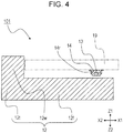
- Fig. 4 is a configuration diagram explaining the current sensor 101 of the first embodiment of the present invention and is a cross-sectional view taken along a line IV-IV illustrated in Fig. 3 .
- the current sensor 101 of the first embodiment of the present invention is configured to include a first current path 12 including a first flat-shaped portion 12f, and a first magnetoelectric conversion element 13 arranged on the first current path 12.
- the insulating substrate 19 arranged so as to face the first current path 12, and a connector, connected to an external control device so as to supply electric power to the current sensor 101 and extract a signal from the current sensor 101 while not illustrated, are provided.
- the first current path 12 is configured to include the first flat-shaped portion 12f and a first convex portion 12w provided to stand from one of end portions 12t of the first current path 12, as illustrated in Fig. 1 to Fig. 4 .
- this first convex portion 12w is formed in a direction in which a current to be measured flows (a Y direction illustrated in Fig. 2 ).
- holding portions used for connecting to and fixing a current path to be measured (a current path intended to be measured) of a device (device to be measured) not illustrated are provided on both the end portion sides of the first current path 12.
- a metal plate such as a copper (Cu) is bent, thereby integrally forming the first flat-shaped portion 12f and the first convex portion 12w. From this, at the time of manufacturing, it is possible to easily manufacture the first flat-shaped portion 12f and the first convex portion 12w from one metal plate. From this, it is possible to reduce the cost of the current sensor 101.
- Cu copper
- the first magnetoelectric conversion element 13 is an element for detecting magnetism generated when the current to be measured flows through the first current path 12, and the first magnetoelectric conversion element 13 is packaged into a magnetic sensor package 14 using, for example, a magnetoresistance effect element (called a GMR (Giant Magneto Resistive) element) utilizing a giant magnetoresistance effect, as illustrated in Fig. 4 .
- a magnetoresistance effect element called a GMR (Giant Magneto Resistive) element
- the first magnetoelectric conversion element 13 is arranged on the first flat-shaped portion 12f, is arranged in the vicinity of the middle of the first flat-shaped portion 12f in the longitudinal direction thereof, and is arranged on the other end portion side of the first current path 12.
- the sensitivity direction of the first magnetoelectric conversion element 13 is arranged so as to face in an X direction illustrated in Fig. 3 .
- the GMR element After the GMR element is manufactured on a silicon substrate, a cut-out chip of the GMR element and lead terminals 14r for extracting a signal are electrically connected and subjected to packaging using a thermosetting synthetic resin, thereby manufacturing this magnetic sensor package 14.
- the magnetic sensor package 14 is soldered to the insulating substrate 19 serving as a circuit substrate by the lead terminals 14r, and is connected to the external control device through a wiring pattern and the connector, not illustrated.
- the first magnetoelectric conversion element 13 is subjected to packaging and arranged, as the magnetic sensor package 14, in the insulating substrate 19, the first magnetoelectric conversion element 13 may be arranged, for example, without change, in other words, may be subjected to so-called bare chip mounting and arranged.
- a widely-known general single-sided printed wiring board is used, and a wiring pattern is formed in a base substrate made of a glass-added epoxy resin by subjecting a metal foil such as copper (Cu), provided on the base substrate, to patterning.
- a metal foil such as copper (Cu)
- Cu copper
- the printed wiring board made of a glass-added epoxy resin is used for the insulating substrate 19, not only this but also, for example, a ceramic wiring board or a flexible wiring board may be used.
- the circuit substrate is suitably used as the insulating substrate 19, not only the circuit substrate but also a structure may be adopted in which a circuit substrate is stacked on the insulating substrate 19 and the magnetic sensor package 14 is mounted thereon.
- Fig. 5 includes cross-sectional views of first current paths 12 of models used in a simulation of the current sensor of the first embodiment of the present invention
- Fig. 5(a) is a model A1
- Fig. 5(b) is a model A2.
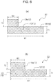
- Fig. 6 includes cross-sectional views of first current paths 12 of models used in a simulation of the current sensor of the first embodiment of the present invention
- Fig. 6(a) is a model B1
- Fig. 6(b) is a model B2.
- the entire length of the first current path 12 was set to 100 (mm)
- the entire width W1 thereof was set to 20 (mm)
- the thickness T1 of the first flat-shaped portion 12f was set to 4 (mm)
- the length of the first convex portion 12w was set to 100 (mm), and the same applied to all the models.
- the width W2 of the first convex portion 12w was set to 4 (mm) and the thickness T2 thereof was set to 4 (mm).
- the width W2 of the first convex portion 12w was set to 4 (mm) and the thickness T2 thereof was set to 10 (mm).
- the width W2 of the first convex portion 12w was set to 6 (mm) and the thickness T2 thereof was set to 4 (mm).
- the width W2 of the first convex portion 12w was set to 8 (mm) and the thickness T2 thereof was set to 4 (mm). And thus, these were caused to vary.
- the current sensor 101 illustrated in Fig. 1 to Fig. 4 embodies this model A1.
- Fig. 7 includes simulation results of the current sensor of the first embodiment of the present invention and includes graphs corresponding to the model A1 in Fig. 5(a) and the model A2 in Fig. 5(b) .
- Fig. 8 includes simulation results of the current sensor of the first embodiment of the present invention and includes graphs corresponding to the model B1 in Fig. 6(a) and the model B2 in Fig. 6(b) .
- a horizontal axis in each of the graphs in Fig. 7 and Fig. 8 is the width W1 of the first current path 12 and indicates a distance from a center (10 (mm) on each of the right and left side).
- P11 in each of the drawings indicates a minimum frequency magnetic flux density in a case of a minimum frequency where the frequency of a current to be measured used in a device (device to be measured) is assumed to be 10 (Hz)
- P2 in each of the drawings indicates a maximum frequency magnetic flux density in a case of a maximum frequency where the frequency of the current to be measured used in the device (device to be measured) is assumed to be 10 (kHz).
- Fig. 26 includes diagrams compared with the current sensor 101 of the first embodiment of the present invention
- Fig. 26(a) is the diagram of a model H101 of a comparative example used in a simulation
- Fig. 26(b) is the graph of a simulation result of the model H101.
- the model H101 of a comparative example the length of a current path H12 was set to 100 (mm), the thickness H1 thereof was set to 4 (mm), and the width H2 thereof was set to 20 (mm), thereby applying same sizes.
- the minimum frequency magnetic flux density P11 and the maximum frequency magnetic flux density P2 are provided in a direction in which the current to be measured flows, it is possible for the minimum frequency magnetic flux density P11 and the maximum frequency magnetic flux density P2 to be brought close to each other and caused to line up more with each other.
- the first magnetoelectric conversion element 13 is arranged at a position on the first current path 12, at which the minimum frequency magnetic flux density P11 and the maximum frequency magnetic flux density P2 substantially coincide with each other.
- the first magnetoelectric conversion element 13 is arranged at a position whose distance from the center is about 7 (mm).
- the first magnetoelectric conversion element 13 is arranged at a position whose distance from the center is about 6.5 (mm).
- the first magnetoelectric conversion element 13 is arranged at a position whose distance from the center is about 5.5 (mm).
- the first magnetoelectric conversion element 13 is arranged at a position whose distance from the center is about 5 (mm). Since, in the current sensor 101 of the present invention, in this way, it is possible to arrange the first magnetoelectric conversion element 13 at a position at which a change in the magnetic flux density associated with a change in the frequency is small, the minimum frequency magnetic flux density P11 and the maximum frequency magnetic flux density P2 are not widely different from each other even if the frequency of the current to be measured changes. Therefore, it is possible to accurately measure a current value.
- the magnetic sensor 910 is provided at the position of the peak (an R portion in Fig. 26(b) ) of the maximum frequency magnetic flux density P2 (a position whose distance from the center is about 9 (mm)), illustrated in Fig. 26(b) , a difference between the minimum frequency magnetic flux density P11 and the maximum frequency magnetic flux density P2 becomes large.
- the sensitivity of a current measured in the current measurement apparatus 900 widely varies and it is difficult to obtain correct measurement accuracy.
- the first convex portion 12w is provided to stand from one of the end portions 12t of the first flat-shaped portion 12f, and the height T2 and the width W2 of the first convex portion 12w are changed, thereby enabling a position, at which a change in the magnetic flux density associated with a change in the frequency is small, to be arbitrarily changed. From this, it is possible to arbitrarily set the arrangement position of the first magnetoelectric conversion element 13.
- the shape of the first convex portion 12w for example, a length, the surface shape of a corner, or the like, it is possible to change a position at which a change in the magnetic flux density associated with a change in the frequency is small, and it is possible to arbitrarily set the arrangement position of the first magnetoelectric conversion element 13.
- the first magnetoelectric conversion element 13 it is possible for the first magnetoelectric conversion element 13 to be arranged so as to be brought closer to the vicinity of the middle of the first current path 12, and compared with a case where the magnetic sensor (magnetoelectric conversion element) 910 is disposed in an outer side portion of the conductor to be measured (current path) 901 in such a manner as the related art, it is possible to reduce the influence of an external magnetizing field from a neighboring current path or the like.
- the first magnetoelectric conversion element 13 is arranged at a position on the first current path 12, at which the minimum frequency magnetic flux density P11 and the maximum frequency magnetic flux density P2 substantially coincide with each other, the first magnetoelectric conversion element 13 may be arranged at a position on the first current path 12, which corresponds to a region in which the minimum frequency magnetic flux density P11 and the maximum frequency magnetic flux density P2 become comparable to each other. As illustrated in, for example, Fig.
- the first magnetoelectric conversion element 13 may be arranged in a region in which the minimum frequency magnetic flux density P11 and the maximum frequency magnetic flux density P2 become comparable to each other, in other words, at a distance of 4.5 (mm) to 7.5 (mm) from the center or preferably a distance of 5.5 (mm) to 7 (mm) therefrom.
- the first magnetoelectric conversion element 13 may be arranged at a distance of 2.5 (mm) to 7 (mm) from the center or preferably a distance of 4.5 (mm) to 6 (mm) therefrom.
- the first convex portion 12w so as to widen a region in which the minimum frequency magnetic flux density P11 and the maximum frequency magnetic flux density P2 become comparable to each other. From this, it is possible to arbitrarily arrange the first magnetoelectric conversion element 13 within the range of this region. Therefore, even in a case where a position at which the current sensor 101 can be disposed is restricted in, for example, use for vehicle installation, it is possible to arrange the first magnetoelectric conversion element 13 at the best possible position.
- the first conductive convex portion 12w long in a direction in which the current to be measured flows is provided in the first current path 12. Therefore, the minimum frequency magnetic flux density P11 serving as a magnetic flux density in a case of passing the current to be measured of the minimum frequency used in a device (device to be measured) and the maximum frequency magnetic flux density P2 serving as a magnetic flux density in a case of passing the current to be measured of the maximum frequency can be brought close to each other and caused to line up more with each other. Therefore, it is possible to arrange the first magnetoelectric conversion element 13 at a position at which a change in the magnetic flux density associated with a change in the frequency is small. From this, the minimum frequency magnetic flux density P11 and the maximum frequency magnetic flux density P2 are not widely different from each other even if the frequency of the current to be measured changes. Therefore, it is possible to accurately measure a current value.
- the first convex portion 12w is provided to stand from one of the end portions 12t of the first flat-shaped portion 12f, it is possible to move, to the central side of the first current path 12, a position at which the minimum frequency magnetic flux density P11 and the maximum frequency magnetic flux density P2 substantially coincide with each other. From this, it is possible for the first magnetoelectric conversion element 13 to be arranged so as to be brought closer to the vicinity of the middle of the first current path 12, and compared with a case where the magnetic sensor (magnetoelectric conversion element) 910 is disposed in an outer side portion of the conductor to be measured (current path) 901 in such a manner as the related art, it is possible to reduce the influence of an external magnetizing field from a neighboring current path or the like.
- a metal plate is bent, thereby integrally forming the first flat-shaped portion 12f and the first convex portion 12w. Therefore, at the time of manufacturing, it is possible to easily manufacture the first flat-shaped portion 12f and the first convex portion 12w from one metal plate. From this, it is possible to reduce the cost of the current sensor 101.
- Fig. 9 is an exploded perspective view explaining a current sensor 102 of a second embodiment of the present invention.
- Fig. 10 is a perspective view explaining the current sensor 102 of the second embodiment of the present invention.
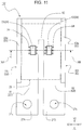
- Fig. 11 is a configuration diagram explaining the current sensor 102 of the second embodiment of the present invention and is a top view viewed from a Z1 side illustrated in Fig. 10 . Note that, in Fig. 10 and Fig. 11 , for ease of explanation, a substrate 29 is made transparent.
- Fig. 12 is a configuration diagram explaining the current sensor 102 of the second embodiment of the present invention and is a cross-sectional view taken along a line XII-XII illustrated in Fig. 11 .
- the current sensor 102 of the second embodiment is different from the first embodiment in that a second current path 62 and a second magnetoelectric conversion element 63 are provided. Note that a same symbol is assigned to the same configuration as that of the first embodiment and the detailed description thereof will be omitted.
- the current sensor 102 of the second embodiment of the present invention includes the first current path 22 including the first flat-shaped portion 22f, the second current path 62 including a second flat-shaped portion 62f, a connection portion 92 connecting one of ends of the first current path 22 and one of ends of the second current path 62 to each other, a first magnetoelectric conversion element 23 arranged on the first current path 22, and the second magnetoelectric conversion element 63 arranged on the second current path 62.
- the substrate 29 arranged so as to face the first current path 22 and the second current path 62, and a connector, connected to an external control device so as to supply electric power to the current sensor 102 and extract a signal from the current sensor 102 while not illustrated, are provided.
- the first current path 22 is configured to include the first flat-shaped portion 22f and a first convex portion 22w provided to stand from one of end portions 22t of the first current path 22, as illustrated in Fig. 9 to Fig. 12 .
- this first convex portion 22w is formed in a direction in which a current to be measured flows (a Y direction illustrated in Fig. 10 ).
- a terminal portion 27A is provided so as to be continuous with the first current path 22, on the other end side of the first current path 22.
- a through hole 27h used for connecting to and fixing a current path to be measured (a current path intended to be measured) of a device (device to be measured) not illustrated is provided.
- the second current path 62 is configured to include the second flat-shaped portion 62f and a second convex portion 62w provided to stand from one of end portions 62t of the second current path 62, as illustrated in Fig. 9 to Fig. 12 .
- this second convex portion 62w is formed in a direction in which the current to be measured flows (the Y direction illustrated in Fig. 10 ).
- a terminal portion 27B is provided so as to be continuous with the second current path 62, on the other end side of the second current path 62.
- a through hole 27k used for connecting to and fixing a current path to be measured (a current path intended to be measured) of a device (device to be measured) not illustrated is provided.
- the first current path 22 and the second current path 62 are disposed in parallel and one of ends of the first current path 22 and one of ends of the second current path 62 are connected to each other by the connection portion 92.
- the first convex portion 22w of the first current path 22 is provided to stand from one of the end portions 22t, located on a side farther away from the second current path 62
- the second convex portion 62w of the second current path 62 is provided to stand from one of the end portions 22t, located on a side farther away from the first current path 22.
- the first convex portion 22w and the second convex portion 62w are arranged so as to face each other. Note that, in the second embodiment of the present invention, the first current path 22, the second current path 62, and the connection portion 92 form a U-shape and the first current path 22 and the second current path 62 are line-symmetrical to each other.
- a metal plate such as a copper (Cu) is bent, thereby integrally forming the first flat-shaped portion 22f, the first convex portion 22w, the connection portion 92, the second flat-shaped portion 62f, and the second convex portion 62w, described above. From this, at the time of manufacturing, it is possible to easily manufacture the first flat-shaped portion 22f, the first convex portion 22w, the connection portion 92, the second flat-shaped portion 62f, and the second convex portion 62w from one metal plate. From this, it is possible to reduce the cost of the current sensor 102.
- Cu copper
- the first magnetoelectric conversion element 23 is an element for detecting magnetism generated when the current to be measured flows through the first current path 22, and the first magnetoelectric conversion element 23 is packaged into a magnetic sensor package 24 using, for example, a magnetoresistance effect element (called a GMR (Giant Magneto Resistive) element) utilizing a giant magnetoresistance effect, as illustrated in Fig. 12 .
- a magnetoresistance effect element called a GMR (Giant Magneto Resistive) element
- the first magnetoelectric conversion element 23 is arranged on a portion of the first flat-shaped portion 22f, from which the first convex portion 22w is provided to stand.
- the sensitivity direction of the first magnetoelectric conversion element 23 is arranged so as to face in an X direction illustrated in Fig. 11 .
- the second magnetoelectric conversion element 63 is an element for detecting magnetism generated when the current to be measured flows through the second current path 62, and in the same way as the first magnetoelectric conversion element 23, the second magnetoelectric conversion element 63 is packaged into a magnetic sensor package 64 using, for example, a magnetoresistance effect element (called a GMR (Giant Magneto Resistive) element) utilizing a giant magnetoresistance effect, as illustrated in Fig. 12 .
- a GMR Green Magneto Resistive
- the second magnetoelectric conversion element 63 is arranged on a portion of the second flat-shaped portion 62f, from which the second convex portion 62w is provided to stand.
- the sensitivity direction of the second magnetoelectric conversion element 63 is arranged so as to face in the X direction illustrated in Fig. 11 .
- the first magnetoelectric conversion element 23 and the second magnetoelectric conversion element 63 are arranged so that the individual directions of the sensitivity axes thereof face in a same direction.
- the GMR elements are manufactured on a silicon substrate, cut-out chips of the GMR elements and lead terminals (24r, 64r) for extracting signals are electrically connected and subjected to packaging using a thermosetting synthetic resin, thereby manufacturing the above-mentioned magnetic sensor packages (24, 64).
- the magnetic sensor package 24 and the magnetic sensor package 64 are soldered to the substrate 29 serving as a circuit substrate by the lead terminals (24r, 64r) and provided on the same substrate 29.
- the magnetic sensor package 24 and the magnetic sensor package 64 are connected to the external control device through wiring patterns and the connector, not illustrated.
- first magnetoelectric conversion element 23 and the second magnetoelectric conversion element 63 are subjected to packaging and arranged, as the magnetic sensor packages (24, 64), in the substrate 29, the first magnetoelectric conversion element 23 and the second magnetoelectric conversion element 63 may be arranged, for example, without change, in other words, may be subjected to so-called bare chip mounting and arranged on the same substrate 29.
- a widely-known general double-sided printed wiring board is used, and a wiring pattern is formed in a base substrate made of a glass-added epoxy resin by subjecting a metal foil such as copper (Cu), provided on the base substrate, to patterning.
- a metal foil such as copper (Cu)
- Cu copper
- the printed wiring board made of a glass-added epoxy resin is used for the substrate 29, not only this but also, for example, a ceramic wiring board or a flexible wiring board may be used.
- the circuit substrate is suitably used as the substrate 29, not only the circuit substrate but also a structure may be adopted in which a circuit substrate is stacked on the substrate 29 and the magnetic sensor packages (24, 64) are mounted thereon.
- Fig. 13 is the cross-sectional view of the first current path 22 and the second current path 62 of a model C1 used in a simulation of the current sensor of the second embodiment of the present invention.
- the entire length of the first current path 22 was set to 100 (mm)
- the entire width W21 thereof was set to 20 (mm)
- the thickness T21 of the first flat-shaped portion 22f was set to 4 (mm)
- the length of the first convex portion 22w was set to 60 (mm)
- the width W22 thereof was set to 4 (mm)
- the height T22 thereof was set to 10 (mm).
- the entire length of the second current path 62 was set to 100 (mm), the entire width W61 thereof was set to 20 (mm), the thickness T61 of the second flat-shaped portion 62f was set to 4 (mm), the length of the second convex portion 62w was set to 60 (mm), the width W62 thereof was set to 4 (mm), and the height T62 thereof was set to 10 (mm).
- a distance W41 between the first current path 22 and the second current path 62 was set to 5 (mm).
- a magnetic flux density in a space 1 (mm) away from the surface of the first current path 22 or the second current path 62 was adopted.
- the current sensor 102 illustrated in Fig. 9 to Fig. 12 embodies this model C1.
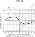
- Fig. 14 is a simulation result of the model C1 of the current sensor of the second embodiment of the present invention.
- a horizontal axis in a graph in Fig. 14 indicates a distance in a width direction at the time of assuming that an intermediate point between the first current path 22 and the second current path 62 is zero, a minus side corresponds to the first current path 22, and a plus side corresponds to the second current path 62.
- a vertical axis in the graph in Fig. 14 indicates a magnetic flux density in a portion in which the first convex portion 22w of the first flat-shaped portion 22f or the second convex portion 62w of the second flat-shaped portion 62f is not provided.
- P21 in the drawing indicates a minimum frequency magnetic flux density in a case of a minimum frequency where the frequency of a current to be measured used in a device (device to be measured) is assumed to be 10 (Hz)
- P22 in the drawing indicates a maximum frequency magnetic flux density in a case of a maximum frequency where the frequency of the current to be measured used in the device (device to be measured) is assumed to be 10 (kHz).
- the minimum frequency magnetic flux density P21 and the maximum frequency magnetic flux density P22 are provided in a direction in which the current to be measured flows, it is possible for the minimum frequency magnetic flux density P21 and the maximum frequency magnetic flux density P22 to be brought close to each other and caused to line up more with each other.
- the second conductive convex portion 62w in a direction in which the current to be measured flows, it is possible for the minimum frequency magnetic flux density P21 and the maximum frequency magnetic flux density P22 to be brought close to each other and caused to line up more with each other.
- the first magnetoelectric conversion element 23 and the second magnetoelectric conversion element 63 are arranged at respective positions on the first current path 22 and the second current path 62, at which the minimum frequency magnetic flux density P21 and the maximum frequency magnetic flux density P22 substantially coincide with each other.
- the first magnetoelectric conversion element 23 is arranged at a position whose distance from the center is about -7.5 (mm) (about 5 (mm) away from the other end portion of the first current path 22).
- the second magnetoelectric conversion element 63 is arranged at a position whose distance from the center is about 7.5 (mm) (about 5 (mm) away from the other end portion of the second current path 62).
- each of the first magnetoelectric conversion element 23 and the second magnetoelectric conversion element 63 at a position at which a change in the magnetic flux density associated with a change in the frequency is small, the minimum frequency magnetic flux density P21 and the maximum frequency magnetic flux density P22 are not widely different from each other even if the frequency of the current to be measured changes. Therefore, it is possible to accurately measure a current value.
- the first magnetoelectric conversion element 23 and the second magnetoelectric conversion element 63 are used and individually provided on the same substrate 29, influences due to an external magnetic field or an internal magnetic field generated when a current flows through a current path (the first current path 22 and the second current path 62) appear, with equal strength, in the two magnetoelectric conversion elements (the first magnetoelectric conversion element 23 and the second magnetoelectric conversion element 63). Therefore, by subjecting outputs from the two magnetoelectric conversion elements (the first magnetoelectric conversion element 23 and the second magnetoelectric conversion element 63) to differential processing, it is possible to more correctly cancel out the influences of the magnetic field. From this, it is possible to reduce the deterioration of the measurement accuracy of the current sensor 102.
- the first magnetoelectric conversion element 23 is arranged at a position on the first current path 22, at which the minimum frequency magnetic flux density P21 and the maximum frequency magnetic flux density P22 substantially coincide with each other, the first magnetoelectric conversion element 23 may be arranged at a position on the first current path 22, which corresponds to a region in which the minimum frequency magnetic flux density P21 and the maximum frequency magnetic flux density P22 become comparable to each other.
- the first magnetoelectric conversion element 23 may be arranged in a region in which the minimum frequency magnetic flux density P21 and the maximum frequency magnetic flux density P22 become comparable to each other, in other words, at a distance of -6 (mm) to -14 (mm) from the center or preferably a distance of -7 (mm) to -9 (mm) therefrom, as illustrated in Fig. 14 (on the minus side).
- the second magnetoelectric conversion element 63 may be arranged at a distance of 6 (mm) to 14 (mm) from the center or preferably a distance of 7 (mm) to 9 (mm) therefrom, as illustrated in Fig. 14 (on the plus side).
- the first convex portion 22w and the second convex portion 62w so as to widen a region in which the minimum frequency magnetic flux density P21 and the maximum frequency magnetic flux density P22 become comparable to each other. From this, it is possible to arbitrarily arrange the first magnetoelectric conversion element 23 and the second magnetoelectric conversion element 63 within the range of this region. Therefore, even in a case where a position at which the current sensor 102 can be disposed is restricted in, for example, use for vehicle installation, it is possible to arrange the first magnetoelectric conversion element 23 and the second magnetoelectric conversion element 63 at the best possible positions.
- the first conductive convex portion 22w long in a direction in which the current to be measured flows is provided in the first current path 22. Therefore, the minimum frequency magnetic flux density P21 serving as a magnetic flux density in a case of passing the current to be measured of the minimum frequency used in a device (device to be measured) and the maximum frequency magnetic flux density P22 serving as a magnetic flux density in a case of passing the current to be measured of the maximum frequency can be brought close to each other and caused to line up more with each other. Therefore, it is possible to arrange the first magnetoelectric conversion element 23 at a position at which a change in the magnetic flux density associated with a change in the frequency is small. From this, the minimum frequency magnetic flux density P21 and the maximum frequency magnetic flux density P22 are not widely different from each other even if the frequency of the current to be measured changes. Therefore, it is possible to accurately measure a current value.
- the second conductive convex portion 62w is provided, in the second current path 62, in a direction in which the current to be measured flows. Therefore, the minimum frequency magnetic flux density P21 serving as a magnetic flux density in a case of passing the current to be measured of the minimum frequency used in the device and the maximum frequency magnetic flux density P22 serving as a magnetic flux density in a case of passing the current to be measured of the maximum frequency can be brought close to each other and caused to line up more with each other. Therefore, it is possible to arrange the second magnetoelectric conversion element 63 at a position at which a change in the magnetic flux density associated with a change in the frequency is small. From this, the minimum frequency magnetic flux density P21 and the maximum frequency magnetic flux density P22 are not widely different from each other even if the frequency of the current to be measured changes. Therefore, it is possible to accurately measure a current value in the second current path 62.
- first magnetoelectric conversion element 23 and the second magnetoelectric conversion element 63 are used and individually provided on the same substrate 29, influences due to an external magnetic field or an internal magnetic field generated when a current flows through the current path (the first current path 22 and the second current path 62) appear, with equal strength, in the two magnetoelectric conversion elements (the first magnetoelectric conversion element 23 and the second magnetoelectric conversion element 63). Therefore, by subjecting outputs from the two magnetoelectric conversion elements (the first magnetoelectric conversion element 23 and the second magnetoelectric conversion element 63) to differential processing, it is possible to more correctly cancel out the influences of the magnetic field. From this, it is possible to reduce the deterioration of the measurement accuracy of the current sensor 102.
- a metal plate such as a copper (Cu) is bent, thereby integrally forming the first flat-shaped portion 22f, the first convex portion 22w, the connection portion 92, the second flat-shaped portion 62f, and the second convex portion 62w. Therefore, at the time of manufacturing, it is possible to easily manufacture the first flat-shaped portion 22f, the first convex portion 22w, the connection portion 92, the second flat-shaped portion 62f, and the second convex portion 62w from one metal plate. From this, it is possible to reduce the cost of the current sensor 102.
- Cu copper
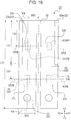
- Fig. 15 is an exploded perspective view explaining a current sensor 103 of a third embodiment of the present invention.
- Fig. 16 is a perspective view explaining the current sensor 103 of the third embodiment of the present invention.
- Fig. 17 is a configuration diagram explaining the current sensor 103 of the third embodiment of the present invention and is a top view viewed from a Z1 side illustrated in Fig. 16 . Note that, in Fig. 16 and Fig. 17 , for ease of explanation, the substrate 29 is made transparent.
- Fig. 18 includes configuration diagrams explaining the current sensor 103 of the third embodiment of the present invention, Fig. 18(a) is a cross-sectional view taken along a line XVII-XVII illustrated in Fig. 17 , and Fig.
- FIG. 18(b) is a cross-sectional view taken along a line XVIII-XVIII illustrated in Fig. 17 .
- the current sensor 103 of the third embodiment is different from the second embodiment in that a first magnetoelectric conversion element 33 and a second magnetoelectric conversion element 73 are provided. Note that a same symbol is assigned to the same configuration as that of the first embodiment or the second embodiment and the detailed description thereof will be omitted.
- the current sensor 103 of the second embodiment of the present invention includes the first current path 22 including the first flat-shaped portion 22f, the second current path 62 including the second flat-shaped portion 62f, the connection portion 92 connecting one of the ends of the first current path 22 and one of the ends of the second current path 62 to each other, the first magnetoelectric conversion element 23 and the first magnetoelectric conversion element 33, arranged on the first current path 22, and the second magnetoelectric conversion element 63 and the second magnetoelectric conversion element 73, arranged on the second current path 62.
- the substrate 29 arranged so as to face the first current path 22 and the second current path 62, and a connector, connected to an external control device so as to supply electric power to the current sensor 103 and extract a signal from the current sensor 103 while not illustrated, are provided.
- connection portion 92 Since the first current path 22, the second current path 62, and the connection portion 92 each have the same structure as that in the second embodiment, the description thereof here will be omitted.
- the first magnetoelectric conversion element 23 is arranged on a first position 22a of the first flat-shaped portion 22f, from which the first convex portion 22w is provided to stand.
- the sensitivity direction of the first magnetoelectric conversion element 23 is arranged so as to face in an X direction illustrated in Fig. 17 .
- the first magnetoelectric conversion element 33 is an element for detecting magnetism generated when the current to be measured flows through the first current path 22, and the first magnetoelectric conversion element 33 is packaged into a magnetic sensor package 34 using, for example, a magnetoresistance effect element (called a GMR (Giant Magneto Resistive) element) utilizing a giant magnetoresistance effect, as illustrated in Fig. 18 .
- a GMR Gate Magneto Resistive
- the first magnetoelectric conversion element 33 is arranged on a third position 22c of the first flat-shaped portion 22f, from which the first convex portion 22w is not provided to stand.
- the sensitivity direction of the first magnetoelectric conversion element 33 is arranged so as to face in the X direction illustrated in Fig. 17 , and faces in the same direction of the sensitivity axis as that of the first magnetoelectric conversion element 23.
- the second magnetoelectric conversion element 63 is arranged on a second position 62b of the second flat-shaped portion 62f, from which the second convex portion 62w is provided to stand.
- the sensitivity direction of the second magnetoelectric conversion element 63 is arranged so as to face in the X direction illustrated in Fig. 17 .
- the second magnetoelectric conversion element 73 is an element for detecting magnetism generated when the current to be measured flows through the second current path 62, and the second magnetoelectric conversion element 73 is packaged into a magnetic sensor package 74 using, for example, a magnetoresistance effect element (called a GMR (Giant Magneto Resistive) element) utilizing a giant magnetoresistance effect, as illustrated in Fig. 18 .
- a GMR Gate Magneto Resistive
- the second magnetoelectric conversion element 73 is arranged on a fourth position 62d of the second flat-shaped portion 62f, from which the second convex portion 62w is not provided to stand.
- the sensitivity direction of the second magnetoelectric conversion element 73 is arranged so as to face in the X direction illustrated in Fig. 17 , and faces in the same direction of the sensitivity axis as that of the second magnetoelectric conversion element 63.
- cut-out chips of the GMR elements and lead terminals (24r, 34r, 64r, 74r) for extracting signals are electrically connected and subjected to packaging using a thermosetting synthetic resin, thereby manufacturing the above-mentioned magnetic sensor packages (24, 34, 64, 74).
- the magnetic sensor packages (24, 34, 64, 74) are soldered to the substrate 29 serving as a circuit substrate by the lead terminals (24r, 34r, 64r, 74r) and provided on the same substrate 29.
- the magnetic sensor packages (24, 34, 64, 74) are connected to the external control device through wiring patterns and the connector, not illustrated.
- magnetizing field analysis utilizing a finite element analysis system was performed with respect to a change in a magnetizing field in a case where a current to be measured whose frequency was different flowed.
- Fig. 19 is the plan view of the first current path 22, the second current path 62, and the connection portion 92 in a model D1 used in a simulation of the current sensor of the third embodiment of the present invention.
- Fig. 20 is the cross-sectional view of the first current path 22 and the second current path 62 in the model D1 used in a simulation of the current sensor of the third embodiment of the present invention and is a cross-sectional view taken along a line XVII-XVII illustrated in Fig. 19 .
- Fig. 21 is a simulation result of the current sensor of the third embodiment of the present invention and is a simulation result in the direction of a line XVII-XVII illustrated in Fig. 19 .
- Fig. 22 illustrates simulation results, Fig.
- Fig. 22(a) is a simulation result in the direction of a line XX-XX illustrated in Fig. 19 in the current sensor of the third embodiment of the present invention
- Fig. 22(b) is a simulation result of a comparative example H131 compared with Fig. 22(a)
- the comparative example H131 is a model in which the first convex portion 22w or the second convex portion 62w, illustrated in Fig. 19 , does not exist.
- P31 in each of the drawings indicates a minimum frequency magnetic flux density in a case of a minimum frequency where the frequency of a current to be measured used in a device (device to be measured) is assumed to be 10 (Hz)
- P32 in each of the drawings indicates a maximum frequency magnetic flux density in a case of a maximum frequency where the frequency of the current to be measured used in the device (device to be measured) is assumed to be 10 (kHz).
- the entire length L21 of the first current path 22 was set to 120 (mm)
- the entire width W21 thereof was set to 20 (mm)
- the thickness T21 of the first flat-shaped portion 22f was set to 4 (mm)
- the length L22 of the first convex portion 22w was set to 60 (mm)
- the width W22 thereof was set to 4 (mm)
- the height T22 thereof was set to 4 (mm).
- the entire length of the second current path 62 was set to 100 (mm), the entire width W61 thereof was set to 20 (mm), the thickness T61 of the second flat-shaped portion 62f was set to 4 (mm), the length of the second convex portion 62w was set to 60 (mm), the width W62 thereof was set to 4 (mm), and the height T62 thereof was set to 4 (mm).
- a length L53 from one of the end portions of each of the first current path 22 and the second current path 62 to the line XVII-XVII was set to 30 (mm)
- a length L63 from one of the end portions of each of the first convex portion 22w and the second convex portion 62w to the line XVIII-XVIII was set to 20 (mm).
- a length between the line XVII-XVII and the line XVIII-XVIII becomes 40 (mm).
- a length W81 from an intermediate point between the first current path 22 and the second current path 62 to the line XX-XX was set to 12.5 (mm).
- a distance W41 between the first current path 22 and the second current path 62 was set to 5 (mm).
- a magnetic flux density in a space 1 (mm) away from the surface of the first current path 22 or the second current path 62 was adopted.
- the current sensor 103 illustrated in Fig. 15 to Fig. 18 embodies this model D1.
- the minimum frequency magnetic flux density P31 and the maximum frequency magnetic flux density P32 are provided in a direction in which the current to be measured flows, it is possible for the minimum frequency magnetic flux density P31 and the maximum frequency magnetic flux density P32 to be brought close to each other and caused to line up more with each other.
- the second conductive convex portion 62w in a direction in which the current to be measured flows, it is possible for the minimum frequency magnetic flux density P31 and the maximum frequency magnetic flux density P32 to be brought close to each other and caused to line up more with each other.
- the first magnetoelectric conversion element 23 and the second magnetoelectric conversion element 63 are arranged at respective positions on the first current path 22 and the second current path 62, at which the minimum frequency magnetic flux density P31 and the maximum frequency magnetic flux density P32 substantially coincide with each other.
- the first magnetoelectric conversion element 23 is arranged at a position whose distance from the center is about -7.5 (mm) (about 5 (mm) away from the other end portion of the first current path 22).
- the second magnetoelectric conversion element 63 is arranged at a position whose distance from the center is about 7.5 (mm) (about 5 (mm) away from the other end portion of the second current path 62).
- each of the first magnetoelectric conversion element 23 and the second magnetoelectric conversion element 63 at a position at which a change in the magnetic flux density associated with a change in the frequency is small, the minimum frequency magnetic flux density P31 and the maximum frequency magnetic flux density P32 are not widely different from each other even if the frequency of the current to be measured changes. Therefore, it is possible to accurately measure a current value.
- the first magnetoelectric conversion element 23 and the second magnetoelectric conversion element 63 are used and individually provided on the same substrate 29, influences due to an external magnetic field or an internal magnetic field generated when a current flows through the current path (the first current path 22 and the second current path 62) appear, with equal strength, in the two magnetoelectric conversion elements (the first magnetoelectric conversion element 23 and the second magnetoelectric conversion element 63). Therefore, by subjecting outputs from the two magnetoelectric conversion elements (the first magnetoelectric conversion element 23 and the second magnetoelectric conversion element 63) to differential processing, it is possible to more correctly cancel out the influences of the magnetic field. From this, it is possible to reduce the deterioration of the measurement accuracy of the current sensor 102.
- the magnetic flux density of a portion of the line XVII-XVII (0 (mm) in the drawing) is smaller than the magnetic flux density of a portion of the line XVIII-XVIII (40 (mm) in the drawing).
- the magnetic flux density of the portion of the line XVII-XVII at the first position 22a from which the first convex portion 22w is provided to stand and the magnetic flux density of the portion of the line XVIII-XVIII at the third position 22c from which the first convex portion 22w is not provided to stand are widely different from each other.
- the first magnetoelectric conversion element 23 is arranged on the first position 22a of the first current path 22, from which the first convex portion 22w is provided to stand, and the first magnetoelectric conversion element 33 is arranged on the third position 22c of the first current path 22, from which the first convex portion 22w is not provided to stand, thereby causing a difference in absolute quantity between a magnetic quantity detected by the first magnetoelectric conversion element 23 and a magnetic quantity detected by the first magnetoelectric conversion element 33. Therefore, it is possible to properly use, for measuring a high current, the first magnetoelectric conversion element 23 arranged at the first position 22a, and it is possible to properly use, for measuring a constant current, the first magnetoelectric conversion element 33 arranged at the third position 22c.
- the arrangement position of the first magnetoelectric conversion element 23 is located at the first position 22a and falls within the range of -15 (mm) (5 (mm) away from one of the end portions of the first convex portion) to +5 (mm) and it is preferred that the arrangement position of the first magnetoelectric conversion element 33 is located at the third position 22c and located in a region -35 (mm) (15 (mm) away from one of the end portions of the first convex portion) or less away.
- the second magnetoelectric conversion element 63 arranged at the second position 62b, and it is possible to properly use, for measuring a low current, the second magnetoelectric conversion element 73 arranged at the fourth position 62d. From this, it is possible to perform wide-range measurement for high current measurement, and it is possible to perform highly accurate measurement for low current measurement.
- the first magnetoelectric conversion element 33 and the second magnetoelectric conversion element 73 are used and individually provided on the same substrate 29, influences due to an external magnetic field or an internal magnetic field generated when a current flows through the current path (the first current path 22 and the second current path 62) appear, with equal strength, in the two magnetoelectric conversion elements (the first magnetoelectric conversion element 33 and the second magnetoelectric conversion element 73). Therefore, by subjecting outputs from the two magnetoelectric conversion elements (the first magnetoelectric conversion element 33 and the second magnetoelectric conversion element 73) to differential processing, it is possible to more correctly cancel out the influences of the magnetic field. From this, it is possible to reduce the deterioration of the measurement accuracy of the current sensor 103.
- the first conductive convex portion 22w long in a direction in which the current to be measured flows is provided in the first current path 22. Therefore, the minimum frequency magnetic flux density P31 serving as a magnetic flux density in a case of passing the current to be measured of the minimum frequency used in a device (device to be measured) and the maximum frequency magnetic flux density P32 serving as a magnetic flux density in a case of passing the current to be measured of the maximum frequency can be brought close to each other and caused to line up more with each other. Therefore, it is possible to arrange the first magnetoelectric conversion element 23 at a position at which a change in the magnetic flux density associated with a change in the frequency is small. From this, the minimum frequency magnetic flux density P31 and the maximum frequency magnetic flux density P32 are not widely different from each other even if the frequency of the current to be measured changes. Therefore, it is possible to accurately measure a current value.
- the second conductive convex portion 62w is provided, in the second current path 62, in a direction in which the current to be measured flows. Therefore, the minimum frequency magnetic flux density P31 serving as a magnetic flux density in a case of passing the current to be measured of the minimum frequency used in the device and the maximum frequency magnetic flux density P32 serving as a magnetic flux density in a case of passing the current to be measured of the maximum frequency can be brought close to each other and caused to line up more with each other. Therefore, it is possible to arrange the second magnetoelectric conversion element 63 at a position at which a change in the magnetic flux density associated with a change in the frequency is small. From this, the minimum frequency magnetic flux density P31 and the maximum frequency magnetic flux density P32 are not widely different from each other even if the frequency of the current to be measured changes. Therefore, it is possible to accurately measure a current value in the second current path 62.
- first magnetoelectric conversion element 23 and the second magnetoelectric conversion element 63 are used and individually provided on the same substrate 29, influences due to an external magnetic field or an internal magnetic field generated when a current flows through the current path (the first current path 22 and the second current path 62) appear, with equal strength, in the two magnetoelectric conversion elements (the first magnetoelectric conversion element 23 and the second magnetoelectric conversion element 63). Therefore, by subjecting outputs from the two magnetoelectric conversion elements (the first magnetoelectric conversion element 23 and the second magnetoelectric conversion element 63) to differential processing, it is possible to more correctly cancel out the influences of the magnetic field. From this, it is possible to reduce the deterioration of the measurement accuracy of the current sensor 102.
- first magnetoelectric conversion element 23 and the second magnetoelectric conversion element 63 arranged at the first position 22a of the first current path 22, from which the first convex portion 22w is provided to stand, and the second position 62b of the second current path 62, from which the second convex portion 62w is provided to stand, respectively, and the first magnetoelectric conversion element 33 and the second magnetoelectric conversion element 73, arranged at the third position 22c of the first current path 22, from which the first convex portion 22w is not provided to stand, and the fourth position 62d of the second current path 62, from which the second convex portion 62w is not provided to stand, respectively, are each separately arranged.
- the first magnetoelectric conversion element 23 and the second magnetoelectric conversion element 63 are arranged at the first position 22a and the second position 62b, respectively, and it is possible to properly use, for measuring a constant current, the first magnetoelectric conversion element 33 and the second magnetoelectric conversion element 73, arranged at the third position 22c and the fourth position 62d, respectively. From this, it is possible to perform wide-range measurement for high current measurement, and it is possible to perform highly accurate measurement for low current measurement.
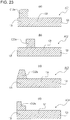
- Fig. 23 includes diagrams explaining examples of modifications to the current sensor 101 of the first embodiment of the present invention
- Fig. 23(a) is a model AC1 of an example 1 of a modification
- Fig. 23(b) is a model AC2 of an example 2 of a modification
- Fig. 23(c) is a model AC3 of an example 3 of a modification
- Fig. 23(d) is a model AC4 of an example 4 of a modification.
- Fig. 24 includes diagrams explaining examples of modifications to the current sensor 101 of the first embodiment of the present invention
- Fig. 24(a) is the plan view of a current sensor C105 of an example 5 of a modification
- Fig. 24(b) is the plan view of a current sensor C106 of an example 6 of a modification.
- Fig. 25 includes diagrams explaining examples of modifications to the current sensor 102 of the second embodiment of the present invention
- Fig. 25(a) is the perspective view of a current sensor C107 of an example 7 of a modification
- Fig. 25(b) is the perspective view of a current sensor C108 of an example 8 of a modification
- Fig. 25(c) is the perspective view of a current sensor C109 of an example 9 of a modification.
- first convex portion 12w is provided to stand from one of the end portions 12t of the first current path 12 and one of the end surfaces of the first flat-shaped portion 12f and one of the surfaces of the first convex portion 12w become flush with each other
- a configuration may be adopted in which, as illustrated in Fig. 23(a) , a first convex portion C12w is provided to stand from one of the end portions 12t of the first current path 12 while one of the end surfaces of the first flat-shaped portion 12f and one of the surfaces of the first convex portion 12w are not flush with each other.
- a configuration may be adopted in which, as illustrated in Fig. 23(b) , a first convex portion C22w is not provided to stand from one of the end portions 12t of the first current path 12.
- the cross-sectional shape of the first convex portion 12w is a rectangular shape
- the cross-sectional shape of the first convex portion 12w is not limited to the rectangular shape, and may be configured in another shape.
- a first convex portion C32w of a trapezoidal shape may be adopted as illustrated in, for example, Fig. 23(c)
- a first convex portion C42w of a shape having a level difference portion as illustrated in, for example, Fig. 23(d) and furthermore, a shape may be formed in a staircase pattern.
- a configuration in which the first convex portion 12w is provided over the entire length in the longitudinal direction of the first current path 12 is adopted
- a configuration in which, as illustrated in Fig. 24(a) , a first convex portion C52w is provided in a portion in the longitudinal direction may be adopted, or a configuration may be adopted where, as illustrated in Fig. 24(b) , a first convex portion C62w in which one of the end surfaces of the first flat-shaped portion 12f and one of the surfaces of the first convex portion 12w are not flush with each other is provided.
- the above-mentioned second embodiment is configured so that the first convex portion 22w of the first current path 22 and the second convex portion 62w of the second current path 62 have the same size and face each other at the same position.
- a configuration in which, as illustrated in, for example, Fig. 25(a) , the first convex portion 22w of the first current path 22 and the second convex portion 62w of the second current path 62 are displaced from each other and face each other may be adopted.
- a configuration is adopted in which the first convex portion 22w of the first current path 22 and the second convex portion 62w of the second current path 62 extend to the respective end portions in the longitudinal directions of the first current path 22 and the second current path 62.
- a configuration may be adopted in which, as illustrated in, for example, Fig. 25(b) , the first convex portion 22w and the second convex portion 62w are provided only in portions of the first current path 22 and the second current path 62, in which the connection portion 92 does not exist, and do not extended to end portions (C72a, C72b) in the longitudinal directions.
- a configuration in which the end portions in the longitudinal direction of each of the first current path 22 and the second current path 62 are opened is adopted
- a configuration may be adopted in which, as illustrated in, for example, Fig. 25(c) , a wall portion 82w provided to stand from respective end portions (C72a, C72b) in the longitudinal directions of the first current path 22 and the second current path 62 and an end portion C92t of the connection portion 92 is provided.
- the GMR elements are suitably used as the first magnetoelectric conversion elements (13, 23, 33) and the second magnetoelectric conversion elements (163, 7), the first magnetoelectric conversion elements (13, 23, 33) and the second magnetoelectric conversion elements (163, 7) only have to be magnetic detecting elements capable of sensing magnetism, are not limited to the above-mentioned embodiments, and may be arbitrarily changed without departing from the scope of the purpose of the present invention.
Description
- The present invention relates to a current sensor for measuring currents to be measured flowing through various kinds of devices, using a magnetoelectric conversion element, and in particular, relates to a current sensor suitable for a case where the frequencies of currents to be measured flowing through various kinds of devices each of which is equipped with an inverter or the like vary.
- In recent years, in order to control or monitor various kinds of devices, usually current sensors attached to the various kinds of devices and configured to measure currents to be measured flowing through the various kinds of devices have been used. As a current sensor of this kind, a method has been well known that utilizes a magnetoelectric conversion element (magnetic detecting element) such as a magnetoresistance effect element or a Hall element, used for sensing a magnetic field generated from a current to be measured flowing through a current path.
- Among the above-mentioned current sensors, such a current measurement apparatus (current sensor) 900 as proposed in
PTL 1 has been generally known that utilizes a flat-shaped conductor to be measured (current path) and a magnetic sensor arranged on an insulating substrate.Fig. 27 is a diagram explaining thecurrent measurement apparatus 900 disclosed inPTL 1 and is a cross-sectional view illustrating a positional relationship between amagnetic sensor 910 and a conductor to be measured 901. As illustrated inFig. 27 , thecurrent measurement apparatus 900 includes the conductor to be measured 901 formed in a printedsubstrate 911 and the magnetic sensor 910 (equipped with a magnetic detecting element) mounted in a printedsubstrate 912 and detects, using themagnetic sensor 910, amagnetic field 920 generated in the width direction of the conductor to be measured 901 when a current to be measured flows through the conductor to be measured 901. - By the way, if the frequency of the current to be measured flowing through such a flat-shaped conductor to be measured 901 increases, the current to be measured is concentrated into end portions of the conductor to be measured 901 by a skin effect, a current density becomes small in the middle of the conductor to be measured 901, and the current density becomes large in the vicinities of ends of the conductor to be measured 901. Therefore, in a case where the
magnetic sensor 910 is disposed in the middle of the conductor to be measured 901 (disposed in an end portion, inFig. 27 ), there has been a problem that themagnetic field 920 in the vicinity of the middle, sensed by themagnetic sensor 910, is reduced and the current sensitivity of thecurrent measurement apparatus 900 is reduced. - Therefore, in the
current measurement apparatus 900 of the related art, as illustrated inFig. 27 , themagnetic sensor 910 is provided at a position located a predetermined distance away from the central position CL of the conductor to be measured 901 in the width direction thereof. From this, it is assumed that it is possible to provide thecurrent measurement apparatus 900 in which the reduction of the measurement sensitivity is suppressed even in a case of a current to be measured whose frequency is high. - PTL 1: Japanese Unexamined Patent Application Publication No.
2005-70037 -
WO 2008/030129 A2 discloses a sensor and procedure for measuring bus bar current with skin effect correction. The sensor contains a bus bar in the form of a ribbon made of a highly conductive material and at least one magnetic sensor which is asymmetrically positioned with respect to the axial axis of a wide side of the bus bar, next to its flat surface. -
US 2012/0081110 A1 discloses a current sensor which comprises a flat housing made of plastic having an underside and an upper side and electrical connections, a current conductor through which the current to be measured flows, and a semiconductor chip having two magnetic field sensors, wherein the component of the magnetic field detected by the two magnetic field sensors points in opposite directions at the locations of the two magnetic field sensors. The semiconductor chip is connected as flipchip to the electrical connections. The current conductor extends from one side wall to the opposite side wall of the housing, is embedded flat in the underside of the housing and is therefore exposed on the underside of the housing. The opposing surfaces of the semiconductor chip and the current conductor are separated by an electrical insulation layer. - However, in the related art, the
magnetic sensor 910 is disposed in the vicinity of an end of the conductor to be measured 901 in accordance with the frequency of the current to be measured, scheduled to be measured. Therefore, there has been a problem that, in a case of being applied to another device utilizing a current to be measured whose frequency is different or in a case where a frequency changes based on a state even in a case of the same device, the sensitivity of a current measured in thecurrent measurement apparatus 900 widely varies and it is difficult to obtain correct measurement accuracy. In addition, as the case where the frequency of the current to be measured changes based on a state, a case may be cited in which, in, for example, an electric vehicle or a hybrid vehicle, the frequency of the current to be measured changes based on states such as at the time of idling, at the time of acceleration, and at the time of regenerative brake. - The present invention solves the above-mentioned problem, and the object thereof is to provide a current sensor capable of accurately measuring a current to be measured even if the frequency of the current to be measured changes.
- In order to solve this problem, a current sensor of the present invention as defined in
claim 1 is provided. - According to this, in the current sensor of the present invention, the first conductive convex portion is provided, in the first current path, in a direction in which the current to be measured flows. Therefore, the minimum frequency magnetic flux density serving as a magnetic flux density in a case of passing the current to be measured of the minimum frequency used in the device and the maximum frequency magnetic flux density serving as a magnetic flux density in a case of passing the current to be measured of the maximum frequency can be brought close to each other and caused to line up more with each other. Therefore, it is possible to arrange the first magnetoelectric conversion element at a position at which a change in the magnetic flux density associated with a change in the frequency is small. From this, the minimum frequency magnetic flux density and the maximum frequency magnetic flux density are not widely different from each other even if the frequency of the current to be measured changes. Therefore, it is possible to accurately measure a current value.
- In addition, in the current sensor of the present invention, the first convex portion is provided to stand from one of end portions of the first flat-shaped portion.
- According to this, it is possible to move, to the central side of the first current path, a position at which the minimum frequency magnetic flux density and the maximum frequency magnetic flux density substantially coincide with each other. From this, it is possible for the first magnetoelectric conversion element to be arranged so as to be brought closer to the vicinity of the middle of the first
current path 12, and compared with a case where the magnetic sensor (magnetoelectric conversion element) 910 is disposed in an outer side portion of the conductor to be measured (current path) 901 in such a manner as the related art, it is possible to reduce the influence of an external magnetizing field from a neighboring current path or the like. - In addition, in the current sensor of the present invention, the first flat-shaped portion and the first convex portion are integrally formed by bending a metal plate.
- According to this, at the time of manufacturing, it is possible to easily manufacture the first flat-shaped portion and the first convex portion from one metal plate. From this, it is possible to reduce the cost of the current sensor.
- In addition, the current sensor of the present invention further includes a second current path including a second flat-shaped portion, and a second magnetoelectric conversion element arranged on the second current path and configured to detect magnetism generated when the current to be measured flows through the second current path, wherein a connection portion connecting one of ends of the first current path and one of ends of the second current path is provided, the first current path and the second current path are disposed in parallel, the other end of the second current path is connected to the device, a second conductive convex portion is provided, in the second current path, in a direction in which the current to be measured flows, the second magnetoelectric conversion element is arranged at a position on the second current path, at which a minimum frequency magnetic flux density serving as a magnetic flux density in a case of passing the current to be measured of a minimum frequency used in the device and a maximum frequency magnetic flux density serving as a magnetic flux density in a case of passing the current to be measured of a maximum frequency used in the device substantially coincide with each other, the first convex portion is provided to stand from one of the end portions, located on a side farther away from the second current path, the second convex portion is provided to stand from an end portion located on a side farther away from the first current path, and the first magnetoelectric conversion element and the second magnetoelectric conversion element are provided on a same substrate.
- According to this, the second conductive convex portion is provided, in the second current path, in a direction in which the current to be measured flows. Therefore, the minimum frequency magnetic flux density serving as a magnetic flux density in a case of passing the current to be measured of the minimum frequency used in the device and the maximum frequency magnetic flux density serving as a magnetic flux density in a case of passing the current to be measured of the maximum frequency can be brought close to each other and caused to line up more with each other. Therefore, it is possible to arrange the second magnetoelectric conversion element at a position at which a change in the magnetic flux density associated with a change in the frequency is small. From this, the minimum frequency magnetic flux density and the maximum frequency magnetic flux density are not widely different from each other even if the frequency of the current to be measured changes. Therefore, it is possible to accurately measure a current value in the second current path. Furthermore, since the first magnetoelectric conversion element and the second magnetoelectric conversion element are used and individually provided on the same substrate, influences due to an external magnetic field or an internal magnetic field generated when a current flows through a current path (the first current path and the second current path) appear, with equal strength, in the two magnetoelectric conversion elements (the first magnetoelectric conversion element and the second magnetoelectric conversion element). Therefore, by subjecting outputs from the two magnetoelectric conversion elements (the first magnetoelectric conversion element and the second magnetoelectric conversion element) to differential processing, it is possible to more correctly cancel out the influences of the magnetic field. From this, it is possible to reduce the deterioration of the measurement accuracy of the current sensor.
- In addition, in the current sensor of the present invention, at least the two or more first magnetoelectric conversion elements are included and at least the two or more second magnetoelectric conversion elements are included, at least one of the first magnetoelectric conversion elements is arranged at a first position of the first flat-shaped portion, from which the first convex portion is provided to stand, at least one of the first magnetoelectric conversion elements is arranged at a third position of the first flat-shaped portion, from which the first convex portion is not provided to stand, at least one of the second magnetoelectric conversion elements is arranged at a second position of the second flat-shaped portion, from which the second convex portion is provided to stand, and at least one of the second magnetoelectric conversion elements is arranged at a fourth position of the second flat-shaped portion, from which the second convex portion is not provided to stand.
- According to this, the first magnetoelectric conversion element and the second magnetoelectric conversion element, arranged at the first position of the first current path, from which the first convex portion is provided to stand, and the second position of the second current path, from which the second convex portion is provided to stand, respectively, and the first magnetoelectric conversion element and the second magnetoelectric conversion element, arranged at the third position of the first current path, from which the first convex portion is not provided to stand, and the fourth position of the second current path, from which the second convex portion is not provided to stand, respectively, are each separately arranged. From this, differences in absolute quantity between respective magnetic quantities detected by the first magnetoelectric conversion element and the second magnetoelectric conversion element, arranged at the first position and the second position, respectively, and respective magnetic quantities detected by the first magnetoelectric conversion element and the second magnetoelectric conversion element, arranged at the third position and the fourth position, respectively, are caused. Therefore, it is possible to properly use, for measuring a high current, the first magnetoelectric conversion element and the second magnetoelectric conversion element, arranged at the first position and the second position, respectively, and it is possible to properly use, for measuring a constant current, the first magnetoelectric conversion element and the second magnetoelectric conversion element, arranged at the third position and the fourth position, respectively. From this, it is possible to perform wide-range measurement for high current measurement, and it is possible to perform highly accurate measurement for low current measurement.
- In addition, in the current sensor of the present invention, the first flat-shaped portion, the first convex portion, the connection portion, the second flat-shaped portion, and the second convex portion are integrally formed by bending a metal plate.
- According to this, at the time of manufacturing, it is possible to easily manufacture the first flat-shaped portion, the first convex portion, the connection portion, the second flat-shaped portion, and the second convex portion from one metal plate. From this, it is possible to reduce the cost of the current sensor.
- In the current sensor of the present invention, the first conductive convex portion long in a direction in which the current to be measured flows is provided in the first current path. Therefore, the minimum frequency magnetic flux density serving as a magnetic flux density in a case of passing the current to be measured of the minimum frequency used in a device (device to be measured) and the maximum frequency magnetic flux density serving as a magnetic flux density in a case of passing the current to be measured of the maximum frequency can be brought close to each other and caused to line up more with each other. Therefore, it is possible to arrange the first magnetoelectric conversion element at a position at which a change in the magnetic flux density associated with a change in the frequency is small. From this, the minimum frequency magnetic flux density and the maximum frequency magnetic flux density are not widely different from each other even if the frequency of the current to be measured changes. Therefore, it is possible to accurately measure a current value.
-
- [
Fig. 1] Fig. 1 is an exploded perspective view explaining a current sensor of a first embodiment of the present invention. - [
Fig. 2] Fig. 2 is a perspective view explaining the current sensor of the first embodiment of the present invention. - [
Fig. 3] Fig. 3 is a configuration diagram explaining the current sensor of the first embodiment of the present invention and is a top view viewed from a Z1 side illustrated inFig. 2 . - [
Fig. 4] Fig. 4 is a configuration diagram explaining the current sensor of the first embodiment of the present invention and is a cross-sectional view taken along a line IV-IV illustrated inFig. 3 . - [
Fig. 5] Fig. 5 includes cross-sectional views of first current paths of two models used in a simulation of the current sensor of the first embodiment of the present invention, which are individually illustrated inFig. 5(a) and Fig. 5(b) . - [
Fig. 6] Fig. 6 includes cross-sectional views of first current paths of two models used in a simulation of the current sensor of the first embodiment of the present invention, which are individually illustrated inFig. 6(a) and Fig. 6(b) . - [
Fig. 7] Fig. 7 includes simulation results of the current sensor of the first embodiment of the present invention and includes graphs corresponding to the models illustrated inFig. 5(a) and Fig. 5(b) . - [
Fig. 8] Fig. 8 includes simulation results of the current sensor of the first embodiment of the present invention and includes graphs corresponding to the models illustrated inFig. 6(a) and Fig. 6(b) . - [
Fig. 9] Fig. 9 is an exploded perspective view explaining a current sensor of a second embodiment of the present invention. - [
Fig. 10] Fig. 10 is a perspective view explaining the current sensor of the second embodiment of the present invention. - [
Fig. 11] Fig. 11 is a configuration diagram explaining the current sensor of the second embodiment of the present invention and is a top view viewed from a Z1 side illustrated inFig. 10 . - [
Fig. 12] Fig. 12 is a configuration diagram explaining the current sensor of the second embodiment of the present invention and is a cross-sectional view taken along a line XII-XII illustrated inFig. 11 . - [
Fig. 13] Fig. 13 is a cross-sectional view of a first current path and a second current path of a model used in a simulation of the current sensor of the second embodiment of the present invention. - [
Fig. 14] Fig. 14 is a graph illustrating a simulation result of the current sensor of the second embodiment of the present invention. - [
Fig. 15] Fig. 15 is an exploded perspective view explaining a current sensor of a third embodiment of the present invention. - [
Fig. 16] Fig. 16 is a perspective view explaining the current sensor of the third embodiment of the present invention. - [
Fig. 17] Fig. 17 is a configuration diagram explaining the current sensor of the third embodiment of the present invention and is a top view viewed from a Z1 side illustrated inFig. 16 . - [
Fig. 18] Fig. 18 includes configuration diagrams explaining the current sensor of the third embodiment of the present invention,Fig. 18(a) is a cross-sectional view taken along a line XVII-XVII illustrated inFig. 17 , andFig. 18(b) is a cross-sectional view taken along a line XVIII-XVIII illustrated inFig. 17 . - [
Fig. 19] Fig. 19 is a plan view of a first current path, a second current path, and a connection portion in a model used in a simulation of the current sensor of the third embodiment of the present invention. - [
Fig. 20] Fig. 20 is a cross-sectional view of the first current path and the second current path in the model used in a simulation of the current sensor of the third embodiment of the present invention and is a cross-sectional view taken along a line XVI-XII illustrated inFig. 19 . - [
Fig. 21] Fig. 21 is a simulation result of the current sensor of the third embodiment of the present invention and is a simulation result in a direction of a line XVII-XVII illustrated inFig. 19 . - [
Fig. 22] Fig. 22 illustrates simulation results,Fig. 22(a) is a simulation result in a direction of a line XX-XX illustrated inFig. 19 in the current sensor of the third embodiment of the present invention, andFig. 22(b) is a simulation result of a comparative example compared withFig. 22(a) . - [
Fig. 23] Fig. 23 includes diagrams explaining examples of modifications to the current sensor of the first embodiment of the present invention,Fig. 23(a) is a model diagram of an example 1 of a modification,Fig. 23(b) is a model diagram of an example 2 of a modification,Fig. 23(c) is a model diagram of an example 3 of a modification, andFig. 23(d) is a model diagram of an example 4 of a modification. - [
Fig. 24] Fig. 24 includes diagrams explaining examples of modifications to the current sensor of the first embodiment of the present invention,Fig. 24(a) is a plan view of an example 5 of a modification, andFig. 24(b) is a plan view of an example 6 of a modification. - [
Fig. 25] Fig. 25 includes diagrams explaining examples of modifications to the current sensor of the second embodiment of the present invention,Fig. 25(a) is a perspective view of an example 7 of a modification,Fig. 25(b) is a perspective view of an example 8 of a modification, andFig. 25(c) is a perspective view of an example 9 of a modification. - [
Fig. 26] Fig. 26 includes diagrams compared with a current sensor of an embodiment of the present invention,Fig. 26(a) is a diagram of a model H101 of a comparative example used in a simulation, andFig. 26(b) is a graph of a simulation result of the model H101. - [
Fig. 27] Fig. 27 is a diagram explaining a current measurement apparatus of the related art and is a cross-sectional view illustrating a positional relationship between a magnetic sensor and a conductor to be measured. - Hereinafter, embodiments of the present invention will be described with reference to the drawings.
-
Fig. 1 is an exploded perspective view explaining acurrent sensor 101 of a first embodiment of the present invention.Fig. 2 is a perspective view explaining thecurrent sensor 101 of the first embodiment of the present invention. In addition, for ease of explanation, an insulatingsubstrate 19 is omitted.Fig. 3 is a configuration diagram explaining thecurrent sensor 101 of the first embodiment of the present invention and is a top view viewed from a Z1 side illustrated inFig. 2 .Fig. 4 is a configuration diagram explaining thecurrent sensor 101 of the first embodiment of the present invention and is a cross-sectional view taken along a line IV-IV illustrated inFig. 3 . - As illustrated in
Fig. 1 to Fig. 4 , thecurrent sensor 101 of the first embodiment of the present invention is configured to include a firstcurrent path 12 including a first flat-shapedportion 12f, and a firstmagnetoelectric conversion element 13 arranged on the firstcurrent path 12. In addition to this, the insulatingsubstrate 19 arranged so as to face the firstcurrent path 12, and a connector, connected to an external control device so as to supply electric power to thecurrent sensor 101 and extract a signal from thecurrent sensor 101 while not illustrated, are provided. - Using a metallic material with a good conductive property such as copper (Cu), the first
current path 12 is configured to include the first flat-shapedportion 12f and a firstconvex portion 12w provided to stand from one ofend portions 12t of the firstcurrent path 12, as illustrated inFig. 1 to Fig. 4 . In addition, this firstconvex portion 12w is formed in a direction in which a current to be measured flows (a Y direction illustrated inFig. 2 ). In addition, while not illustrated, holding portions used for connecting to and fixing a current path to be measured (a current path intended to be measured) of a device (device to be measured) not illustrated are provided on both the end portion sides of the firstcurrent path 12. - In addition, a metal plate such as a copper (Cu) is bent, thereby integrally forming the first flat-shaped
portion 12f and the firstconvex portion 12w. From this, at the time of manufacturing, it is possible to easily manufacture the first flat-shapedportion 12f and the firstconvex portion 12w from one metal plate. From this, it is possible to reduce the cost of thecurrent sensor 101. - The first
magnetoelectric conversion element 13 is an element for detecting magnetism generated when the current to be measured flows through the firstcurrent path 12, and the firstmagnetoelectric conversion element 13 is packaged into amagnetic sensor package 14 using, for example, a magnetoresistance effect element (called a GMR (Giant Magneto Resistive) element) utilizing a giant magnetoresistance effect, as illustrated inFig. 4 . In addition, as illustrated inFig. 2 andFig. 3 , the firstmagnetoelectric conversion element 13 is arranged on the first flat-shapedportion 12f, is arranged in the vicinity of the middle of the first flat-shapedportion 12f in the longitudinal direction thereof, and is arranged on the other end portion side of the firstcurrent path 12. In addition, the sensitivity direction of the firstmagnetoelectric conversion element 13 is arranged so as to face in an X direction illustrated inFig. 3 . - After the GMR element is manufactured on a silicon substrate, a cut-out chip of the GMR element and lead
terminals 14r for extracting a signal are electrically connected and subjected to packaging using a thermosetting synthetic resin, thereby manufacturing thismagnetic sensor package 14. In addition, themagnetic sensor package 14 is soldered to the insulatingsubstrate 19 serving as a circuit substrate by thelead terminals 14r, and is connected to the external control device through a wiring pattern and the connector, not illustrated. In addition, while the firstmagnetoelectric conversion element 13 is subjected to packaging and arranged, as themagnetic sensor package 14, in the insulatingsubstrate 19, the firstmagnetoelectric conversion element 13 may be arranged, for example, without change, in other words, may be subjected to so-called bare chip mounting and arranged. - In the insulating
substrate 19, a widely-known general single-sided printed wiring board is used, and a wiring pattern is formed in a base substrate made of a glass-added epoxy resin by subjecting a metal foil such as copper (Cu), provided on the base substrate, to patterning. As illustrated inFig. 3 andFig. 4 , in the insulatingsubstrate 19, onemagnetic sensor package 14 into which the firstmagnetoelectric conversion element 13 is packaged is mounted. Note that while the printed wiring board made of a glass-added epoxy resin is used for the insulatingsubstrate 19, not only this but also, for example, a ceramic wiring board or a flexible wiring board may be used. In addition, while, in the first embodiment of the present invention, the circuit substrate is suitably used as the insulatingsubstrate 19, not only the circuit substrate but also a structure may be adopted in which a circuit substrate is stacked on the insulatingsubstrate 19 and themagnetic sensor package 14 is mounted thereon. - Regarding the
current sensor 101 configured as above, magnetizing field analysis utilizing a finite element analysis system was performed with respect to a change in a magnetizing field in a case where a current to be measured whose frequency was different flowed.Fig. 5 includes cross-sectional views of firstcurrent paths 12 of models used in a simulation of the current sensor of the first embodiment of the present invention,Fig. 5(a) is a model A1, andFig. 5(b) is a model A2. In addition,Fig. 6 includes cross-sectional views of firstcurrent paths 12 of models used in a simulation of the current sensor of the first embodiment of the present invention,Fig. 6(a) is a model B1, andFig. 6(b) is a model B2. - As for numerical values used in the simulation (see
Fig. 5 andFig. 6 ), the entire length of the firstcurrent path 12 was set to 100 (mm), the entire width W1 thereof was set to 20 (mm), the thickness T1 of the first flat-shapedportion 12f was set to 4 (mm), the length of the firstconvex portion 12w was set to 100 (mm), and the same applied to all the models. On the other hand, as for the model A1, the width W2 of the firstconvex portion 12w was set to 4 (mm) and the thickness T2 thereof was set to 4 (mm). As for the model A2, the width W2 of the firstconvex portion 12w was set to 4 (mm) and the thickness T2 thereof was set to 10 (mm). As for the model B1, the width W2 of the firstconvex portion 12w was set to 6 (mm) and the thickness T2 thereof was set to 4 (mm). The width W2 of the firstconvex portion 12w was set to 8 (mm) and the thickness T2 thereof was set to 4 (mm). And thus, these were caused to vary. In addition, thecurrent sensor 101 illustrated inFig. 1 to Fig. 4 embodies this model A1. - In addition,
Fig. 7 includes simulation results of the current sensor of the first embodiment of the present invention and includes graphs corresponding to the model A1 inFig. 5(a) and the model A2 inFig. 5(b) .Fig. 8 includes simulation results of the current sensor of the first embodiment of the present invention and includes graphs corresponding to the model B1 inFig. 6(a) and the model B2 inFig. 6(b) . A horizontal axis in each of the graphs inFig. 7 andFig. 8 is the width W1 of the firstcurrent path 12 and indicates a distance from a center (10 (mm) on each of the right and left side). In addition, a vertical axis in each of the graphs inFig. 7 andFig. 8 indicates a magnetic flux density in a portion in which the firstconvex portion 12w is not provided in the first flat-shapedportion 12f. In addition, P11 in each of the drawings indicates a minimum frequency magnetic flux density in a case of a minimum frequency where the frequency of a current to be measured used in a device (device to be measured) is assumed to be 10 (Hz), and P2 in each of the drawings indicates a maximum frequency magnetic flux density in a case of a maximum frequency where the frequency of the current to be measured used in the device (device to be measured) is assumed to be 10 (kHz). - In addition, for the sake of comparison, a simulation was performed with respect to the configuration of the related art in which the first
convex portion 12w does not exist in the firstcurrent path 12.Fig. 26 includes diagrams compared with thecurrent sensor 101 of the first embodiment of the present invention,Fig. 26(a) is the diagram of a model H101 of a comparative example used in a simulation, andFig. 26(b) is the graph of a simulation result of the model H101. In addition, regarding the model H101 of a comparative example, the length of a current path H12 was set to 100 (mm), the thickness H1 thereof was set to 4 (mm), and the width H2 thereof was set to 20 (mm), thereby applying same sizes. - As a result, compared with a case where a large difference in the magnetic flux density is generated by a difference between the low frequency and the high frequency of the current to be measured in such a manner as in
Fig. 26(b) , a difference in the magnetic flux density, due to a difference between the low frequency and the high frequency of the current to be measured, in other words, a difference between the minimum frequency magnetic flux density P11 and the maximum frequency magnetic flux density P2, became small above the first flat-shapedportion 12f in which the firstconvex portion 12w is not provided, as illustrated inFig. 7 andFig. 8 . It is conceivable that the reason is that a magnetizing field around the firstcurrent path 12 was changed by providing the firstconvex portion 12w. Accordingly, by providing the first conductiveconvex portion 12w in a direction in which the current to be measured flows, it is possible for the minimum frequency magnetic flux density P11 and the maximum frequency magnetic flux density P2 to be brought close to each other and caused to line up more with each other. - From this, it is preferred that the first
magnetoelectric conversion element 13 is arranged at a position on the firstcurrent path 12, at which the minimum frequency magnetic flux density P11 and the maximum frequency magnetic flux density P2 substantially coincide with each other. As illustrated in, for example,Fig. 7 , in a case of the model A1, it is preferable that, on the first flat-shapedportion 12f in which the firstconvex portion 12w of the firstcurrent path 12 is not provided, the firstmagnetoelectric conversion element 13 is arranged at a position whose distance from the center is about 7 (mm). In addition, in a case of the model A2, it is preferable that, on the first flat-shapedportion 12f in which the firstconvex portion 12w of the firstcurrent path 12 is not provided, the firstmagnetoelectric conversion element 13 is arranged at a position whose distance from the center is about 6.5 (mm). In addition, as illustrated inFig. 8 , in a case of the model B1, it is preferable that, on the first flat-shapedportion 12f in which the firstconvex portion 12w of the firstcurrent path 12 is not provided, the firstmagnetoelectric conversion element 13 is arranged at a position whose distance from the center is about 5.5 (mm). In addition, in a case of the model B2, it is preferable that, on the first flat-shapedportion 12f in which the firstconvex portion 12w of the firstcurrent path 12 is not provided, the firstmagnetoelectric conversion element 13 is arranged at a position whose distance from the center is about 5 (mm). Since, in thecurrent sensor 101 of the present invention, in this way, it is possible to arrange the firstmagnetoelectric conversion element 13 at a position at which a change in the magnetic flux density associated with a change in the frequency is small, the minimum frequency magnetic flux density P11 and the maximum frequency magnetic flux density P2 are not widely different from each other even if the frequency of the current to be measured changes. Therefore, it is possible to accurately measure a current value. - On the other hand, since, in the
current measurement apparatus 900 of the related art, in order to suppress the reduction of the current sensitivity, themagnetic sensor 910 is provided at the position of the peak (an R portion inFig. 26(b) ) of the maximum frequency magnetic flux density P2 (a position whose distance from the center is about 9 (mm)), illustrated inFig. 26(b) , a difference between the minimum frequency magnetic flux density P11 and the maximum frequency magnetic flux density P2 becomes large. Therefore, in a case of being applied to another device utilizing a current to be measured whose frequency is different or in a case where a frequency changes based on a state even in a case of the same device, the sensitivity of a current measured in thecurrent measurement apparatus 900 widely varies and it is difficult to obtain correct measurement accuracy. - In addition, from results illustrated in
Fig. 7 andFig. 8 , the firstconvex portion 12w is provided to stand from one of theend portions 12t of the first flat-shapedportion 12f, and the height T2 and the width W2 of the firstconvex portion 12w are changed, thereby enabling a position, at which a change in the magnetic flux density associated with a change in the frequency is small, to be arbitrarily changed. From this, it is possible to arbitrarily set the arrangement position of the firstmagnetoelectric conversion element 13. In addition, while not illustrated, by changing the shape of the firstconvex portion 12w, for example, a length, the surface shape of a corner, or the like, it is possible to change a position at which a change in the magnetic flux density associated with a change in the frequency is small, and it is possible to arbitrarily set the arrangement position of the firstmagnetoelectric conversion element 13. - In addition, from results illustrated in
Fig. 7 andFig. 8 , since the firstconvex portion 12w is provided to stand from one of theend portions 12t of the first flat-shapedportion 12f, it is possible to move, to the central side of the firstcurrent path 12, a position at which the minimum frequency magnetic flux density P11 and the maximum frequency magnetic flux density P2 substantially coincide with each other. From this, it is possible for the firstmagnetoelectric conversion element 13 to be arranged so as to be brought closer to the vicinity of the middle of the firstcurrent path 12, and compared with a case where the magnetic sensor (magnetoelectric conversion element) 910 is disposed in an outer side portion of the conductor to be measured (current path) 901 in such a manner as the related art, it is possible to reduce the influence of an external magnetizing field from a neighboring current path or the like. - In addition, the existence of this advantageous effect enables the following problem to be solved. By changing the height H2 or the width W2 of the first
convex portion 12w, it is possible to arbitrarily change a position at which the minimum frequency magnetic flux density P11 and the maximum frequency magnetic flux density P2 substantially coincide with each other. Therefore, it is possible to solve a problem that, in, for example, use for vehicle installation, a position at which a current sensor can be disposed is restricted and in such acurrent measurement apparatus 900 as the related art, it is difficult to arrange the magnetic sensor (magnetoelectric conversion element) 910 at the best possible position. - In addition, while it is preferred that the first
magnetoelectric conversion element 13 is arranged at a position on the firstcurrent path 12, at which the minimum frequency magnetic flux density P11 and the maximum frequency magnetic flux density P2 substantially coincide with each other, the firstmagnetoelectric conversion element 13 may be arranged at a position on the firstcurrent path 12, which corresponds to a region in which the minimum frequency magnetic flux density P11 and the maximum frequency magnetic flux density P2 become comparable to each other. As illustrated in, for example,Fig. 7(b) , in a case of the model A2, the firstmagnetoelectric conversion element 13 may be arranged in a region in which the minimum frequency magnetic flux density P11 and the maximum frequency magnetic flux density P2 become comparable to each other, in other words, at a distance of 4.5 (mm) to 7.5 (mm) from the center or preferably a distance of 5.5 (mm) to 7 (mm) therefrom. As illustrated in, for example,Fig. 8(b) , in a case of the model B2, the firstmagnetoelectric conversion element 13 may be arranged at a distance of 2.5 (mm) to 7 (mm) from the center or preferably a distance of 4.5 (mm) to 6 (mm) therefrom. In this way, it is possible to provide the firstconvex portion 12w so as to widen a region in which the minimum frequency magnetic flux density P11 and the maximum frequency magnetic flux density P2 become comparable to each other. From this, it is possible to arbitrarily arrange the firstmagnetoelectric conversion element 13 within the range of this region. Therefore, even in a case where a position at which thecurrent sensor 101 can be disposed is restricted in, for example, use for vehicle installation, it is possible to arrange the firstmagnetoelectric conversion element 13 at the best possible position. - Advantageous effects in the
current sensor 101 of the first embodiment configured as above will be described below. - In the
current sensor 101 of the first embodiment of the present invention, the first conductiveconvex portion 12w long in a direction in which the current to be measured flows is provided in the firstcurrent path 12. Therefore, the minimum frequency magnetic flux density P11 serving as a magnetic flux density in a case of passing the current to be measured of the minimum frequency used in a device (device to be measured) and the maximum frequency magnetic flux density P2 serving as a magnetic flux density in a case of passing the current to be measured of the maximum frequency can be brought close to each other and caused to line up more with each other. Therefore, it is possible to arrange the firstmagnetoelectric conversion element 13 at a position at which a change in the magnetic flux density associated with a change in the frequency is small. From this, the minimum frequency magnetic flux density P11 and the maximum frequency magnetic flux density P2 are not widely different from each other even if the frequency of the current to be measured changes. Therefore, it is possible to accurately measure a current value. - In addition, since the first
convex portion 12w is provided to stand from one of theend portions 12t of the first flat-shapedportion 12f, it is possible to move, to the central side of the firstcurrent path 12, a position at which the minimum frequency magnetic flux density P11 and the maximum frequency magnetic flux density P2 substantially coincide with each other. From this, it is possible for the firstmagnetoelectric conversion element 13 to be arranged so as to be brought closer to the vicinity of the middle of the firstcurrent path 12, and compared with a case where the magnetic sensor (magnetoelectric conversion element) 910 is disposed in an outer side portion of the conductor to be measured (current path) 901 in such a manner as the related art, it is possible to reduce the influence of an external magnetizing field from a neighboring current path or the like. - In addition, a metal plate is bent, thereby integrally forming the first flat-shaped
portion 12f and the firstconvex portion 12w. Therefore, at the time of manufacturing, it is possible to easily manufacture the first flat-shapedportion 12f and the firstconvex portion 12w from one metal plate. From this, it is possible to reduce the cost of thecurrent sensor 101. -
Fig. 9 is an exploded perspective view explaining acurrent sensor 102 of a second embodiment of the present invention.Fig. 10 is a perspective view explaining thecurrent sensor 102 of the second embodiment of the present invention.Fig. 11 is a configuration diagram explaining thecurrent sensor 102 of the second embodiment of the present invention and is a top view viewed from a Z1 side illustrated inFig. 10 . Note that, inFig. 10 andFig. 11 , for ease of explanation, asubstrate 29 is made transparent.Fig. 12 is a configuration diagram explaining thecurrent sensor 102 of the second embodiment of the present invention and is a cross-sectional view taken along a line XII-XII illustrated inFig. 11 . In addition, thecurrent sensor 102 of the second embodiment is different from the first embodiment in that a secondcurrent path 62 and a secondmagnetoelectric conversion element 63 are provided. Note that a same symbol is assigned to the same configuration as that of the first embodiment and the detailed description thereof will be omitted. - As illustrated in
Fig. 9 to Fig. 12 , thecurrent sensor 102 of the second embodiment of the present invention includes the firstcurrent path 22 including the first flat-shapedportion 22f, the secondcurrent path 62 including a second flat-shapedportion 62f, aconnection portion 92 connecting one of ends of the firstcurrent path 22 and one of ends of the secondcurrent path 62 to each other, a firstmagnetoelectric conversion element 23 arranged on the firstcurrent path 22, and the secondmagnetoelectric conversion element 63 arranged on the secondcurrent path 62. In addition to this, thesubstrate 29 arranged so as to face the firstcurrent path 22 and the secondcurrent path 62, and a connector, connected to an external control device so as to supply electric power to thecurrent sensor 102 and extract a signal from thecurrent sensor 102 while not illustrated, are provided. - Using a metallic material with a good conductive property such as copper (Cu), the first
current path 22 is configured to include the first flat-shapedportion 22f and a firstconvex portion 22w provided to stand from one ofend portions 22t of the firstcurrent path 22, as illustrated inFig. 9 to Fig. 12 . In addition, this firstconvex portion 22w is formed in a direction in which a current to be measured flows (a Y direction illustrated inFig. 10 ). - In addition, as illustrated in
Fig. 9 to Fig. 11 , aterminal portion 27A is provided so as to be continuous with the firstcurrent path 22, on the other end side of the firstcurrent path 22. In addition, in thisterminal portion 27A, a throughhole 27h used for connecting to and fixing a current path to be measured (a current path intended to be measured) of a device (device to be measured) not illustrated is provided. - Using a metallic material with a good conductive property such as copper (Cu), the second
current path 62 is configured to include the second flat-shapedportion 62f and a secondconvex portion 62w provided to stand from one ofend portions 62t of the secondcurrent path 62, as illustrated inFig. 9 to Fig. 12 . In addition, this secondconvex portion 62w is formed in a direction in which the current to be measured flows (the Y direction illustrated inFig. 10 ). - In addition, as illustrated in
Fig. 9 to Fig. 11 , aterminal portion 27B is provided so as to be continuous with the secondcurrent path 62, on the other end side of the secondcurrent path 62. In addition, in thisterminal portion 27B, a throughhole 27k used for connecting to and fixing a current path to be measured (a current path intended to be measured) of a device (device to be measured) not illustrated is provided. - As illustrated in
Fig. 9 to Fig. 11 , the firstcurrent path 22 and the secondcurrent path 62 are disposed in parallel and one of ends of the firstcurrent path 22 and one of ends of the secondcurrent path 62 are connected to each other by theconnection portion 92. At that time, the firstconvex portion 22w of the firstcurrent path 22 is provided to stand from one of theend portions 22t, located on a side farther away from the secondcurrent path 62, and the secondconvex portion 62w of the secondcurrent path 62 is provided to stand from one of theend portions 22t, located on a side farther away from the firstcurrent path 22. In addition, the firstconvex portion 22w and the secondconvex portion 62w are arranged so as to face each other. Note that, in the second embodiment of the present invention, the firstcurrent path 22, the secondcurrent path 62, and theconnection portion 92 form a U-shape and the firstcurrent path 22 and the secondcurrent path 62 are line-symmetrical to each other. - In addition, a metal plate such as a copper (Cu) is bent, thereby integrally forming the first flat-shaped
portion 22f, the firstconvex portion 22w, theconnection portion 92, the second flat-shapedportion 62f, and the secondconvex portion 62w, described above. From this, at the time of manufacturing, it is possible to easily manufacture the first flat-shapedportion 22f, the firstconvex portion 22w, theconnection portion 92, the second flat-shapedportion 62f, and the secondconvex portion 62w from one metal plate. From this, it is possible to reduce the cost of thecurrent sensor 102. - The first
magnetoelectric conversion element 23 is an element for detecting magnetism generated when the current to be measured flows through the firstcurrent path 22, and the firstmagnetoelectric conversion element 23 is packaged into amagnetic sensor package 24 using, for example, a magnetoresistance effect element (called a GMR (Giant Magneto Resistive) element) utilizing a giant magnetoresistance effect, as illustrated inFig. 12 . In addition, as illustrated inFig. 10 to Fig. 12 , the firstmagnetoelectric conversion element 23 is arranged on a portion of the first flat-shapedportion 22f, from which the firstconvex portion 22w is provided to stand. In addition, the sensitivity direction of the firstmagnetoelectric conversion element 23 is arranged so as to face in an X direction illustrated inFig. 11 . - The second
magnetoelectric conversion element 63 is an element for detecting magnetism generated when the current to be measured flows through the secondcurrent path 62, and in the same way as the firstmagnetoelectric conversion element 23, the secondmagnetoelectric conversion element 63 is packaged into amagnetic sensor package 64 using, for example, a magnetoresistance effect element (called a GMR (Giant Magneto Resistive) element) utilizing a giant magnetoresistance effect, as illustrated inFig. 12 . In addition, as illustrated inFig. 10 to Fig. 12 , the secondmagnetoelectric conversion element 63 is arranged on a portion of the second flat-shapedportion 62f, from which the secondconvex portion 62w is provided to stand. In addition, the sensitivity direction of the secondmagnetoelectric conversion element 63 is arranged so as to face in the X direction illustrated inFig. 11 . In addition, since differential processing is performed using the firstmagnetoelectric conversion element 23 and the secondmagnetoelectric conversion element 63, the firstmagnetoelectric conversion element 23 and the secondmagnetoelectric conversion element 63 are arranged so that the individual directions of the sensitivity axes thereof face in a same direction. - After the GMR elements are manufactured on a silicon substrate, cut-out chips of the GMR elements and lead terminals (24r, 64r) for extracting signals are electrically connected and subjected to packaging using a thermosetting synthetic resin, thereby manufacturing the above-mentioned magnetic sensor packages (24, 64). In addition, the
magnetic sensor package 24 and themagnetic sensor package 64 are soldered to thesubstrate 29 serving as a circuit substrate by the lead terminals (24r, 64r) and provided on thesame substrate 29. In addition, themagnetic sensor package 24 and themagnetic sensor package 64 are connected to the external control device through wiring patterns and the connector, not illustrated. Note that while the firstmagnetoelectric conversion element 23 and the secondmagnetoelectric conversion element 63 are subjected to packaging and arranged, as the magnetic sensor packages (24, 64), in thesubstrate 29, the firstmagnetoelectric conversion element 23 and the secondmagnetoelectric conversion element 63 may be arranged, for example, without change, in other words, may be subjected to so-called bare chip mounting and arranged on thesame substrate 29. - In the
substrate 29, a widely-known general double-sided printed wiring board is used, and a wiring pattern is formed in a base substrate made of a glass-added epoxy resin by subjecting a metal foil such as copper (Cu), provided on the base substrate, to patterning. As illustrated inFig. 3 andFig. 4 , in thesubstrate 29, two magnetic sensor packages (4, 64) into which the firstmagnetoelectric conversion element 23 are the secondmagnetoelectric conversion element 63 are packaged, respectively, are mounted. Note that while the printed wiring board made of a glass-added epoxy resin is used for thesubstrate 29, not only this but also, for example, a ceramic wiring board or a flexible wiring board may be used. In addition, while, in the second embodiment of the present invention, the circuit substrate is suitably used as thesubstrate 29, not only the circuit substrate but also a structure may be adopted in which a circuit substrate is stacked on thesubstrate 29 and the magnetic sensor packages (24, 64) are mounted thereon. - Regarding the
current sensor 102 configured as above, magnetizing field analysis utilizing a finite element analysis system was performed with respect to a change in a magnetizing field in a case where a current to be measured whose frequency was different flowed.Fig. 13 is the cross-sectional view of the firstcurrent path 22 and the secondcurrent path 62 of a model C1 used in a simulation of the current sensor of the second embodiment of the present invention. - As for numerical values used in the simulation (see
Fig. 13 ), the entire length of the firstcurrent path 22 was set to 100 (mm), the entire width W21 thereof was set to 20 (mm), the thickness T21 of the first flat-shapedportion 22f was set to 4 (mm), the length of the firstconvex portion 22w was set to 60 (mm), the width W22 thereof was set to 4 (mm), and the height T22 thereof was set to 10 (mm). On the other hand, the entire length of the secondcurrent path 62 was set to 100 (mm), the entire width W61 thereof was set to 20 (mm), the thickness T61 of the second flat-shapedportion 62f was set to 4 (mm), the length of the secondconvex portion 62w was set to 60 (mm), the width W62 thereof was set to 4 (mm), and the height T62 thereof was set to 10 (mm). In addition, a distance W41 between the firstcurrent path 22 and the secondcurrent path 62 was set to 5 (mm). In addition, a magnetic flux density in a space 1 (mm) away from the surface of the firstcurrent path 22 or the secondcurrent path 62 was adopted. In addition, thecurrent sensor 102 illustrated inFig. 9 to Fig. 12 embodies this model C1. - In addition,
Fig. 14 is a simulation result of the model C1 of the current sensor of the second embodiment of the present invention. A horizontal axis in a graph inFig. 14 indicates a distance in a width direction at the time of assuming that an intermediate point between the firstcurrent path 22 and the secondcurrent path 62 is zero, a minus side corresponds to the firstcurrent path 22, and a plus side corresponds to the secondcurrent path 62. In addition, a vertical axis in the graph inFig. 14 indicates a magnetic flux density in a portion in which the firstconvex portion 22w of the first flat-shapedportion 22f or the secondconvex portion 62w of the second flat-shapedportion 62f is not provided. In addition, P21 in the drawing indicates a minimum frequency magnetic flux density in a case of a minimum frequency where the frequency of a current to be measured used in a device (device to be measured) is assumed to be 10 (Hz), and P22 in the drawing indicates a maximum frequency magnetic flux density in a case of a maximum frequency where the frequency of the current to be measured used in the device (device to be measured) is assumed to be 10 (kHz). - As a result, compared with a case where a large difference in the magnetic flux density is generated by a difference between the low frequency and the high frequency of the current to be measured in such a manner as in
Fig. 26(b) , a difference in the magnetic flux density, due to a difference between the low frequency and the high frequency of the current to be measured, in other words, a difference between the minimum frequency magnetic flux density P21 and the maximum frequency magnetic flux density P22, became small above the first flat-shapedportion 22f in which the firstconvex portion 22w of the firstcurrent path 22 is not provided, as illustrated inFig. 14 (on the minus side). It is conceivable that the reason is that a magnetizing field around the firstcurrent path 22 was changed by providing the firstconvex portion 22w. Accordingly, by providing the first conductiveconvex portion 22w in a direction in which the current to be measured flows, it is possible for the minimum frequency magnetic flux density P21 and the maximum frequency magnetic flux density P22 to be brought close to each other and caused to line up more with each other. - In addition, as illustrated in
Fig. 14 (on the plus side), in the secondcurrent path 62, a difference in the magnetic flux density, due to a difference between the low frequency and the high frequency of the current to be measured, in other words, a difference between the minimum frequency magnetic flux density P21 and the maximum frequency magnetic flux density P22, became small above the second flat-shapedportion 62f in which the secondconvex portion 62w is not provided. It is conceivable that the reason is that a magnetizing field around the secondcurrent path 62 was changed by providing the secondconvex portion 62w. Accordingly, by providing the second conductiveconvex portion 62w in a direction in which the current to be measured flows, it is possible for the minimum frequency magnetic flux density P21 and the maximum frequency magnetic flux density P22 to be brought close to each other and caused to line up more with each other. - From the above, it is preferred that the first
magnetoelectric conversion element 23 and the secondmagnetoelectric conversion element 63 are arranged at respective positions on the firstcurrent path 22 and the secondcurrent path 62, at which the minimum frequency magnetic flux density P21 and the maximum frequency magnetic flux density P22 substantially coincide with each other. For example, in a case of such a model C1 as illustrated inFig. 14 , it is preferable that, on the first flat-shapedportion 22f in which the firstconvex portion 22w of the firstcurrent path 22 is not provided, the firstmagnetoelectric conversion element 23 is arranged at a position whose distance from the center is about -7.5 (mm) (about 5 (mm) away from the other end portion of the first current path 22). In addition, it is preferable that, on the second flat-shapedportion 62f in which the secondconvex portion 62w of the secondcurrent path 62 is not provided, the secondmagnetoelectric conversion element 63 is arranged at a position whose distance from the center is about 7.5 (mm) (about 5 (mm) away from the other end portion of the second current path 62). Since, in thecurrent sensor 102 of the present invention, in this way, it is possible to arrange each of the firstmagnetoelectric conversion element 23 and the secondmagnetoelectric conversion element 63 at a position at which a change in the magnetic flux density associated with a change in the frequency is small, the minimum frequency magnetic flux density P21 and the maximum frequency magnetic flux density P22 are not widely different from each other even if the frequency of the current to be measured changes. Therefore, it is possible to accurately measure a current value. - Furthermore, since the first
magnetoelectric conversion element 23 and the secondmagnetoelectric conversion element 63 are used and individually provided on thesame substrate 29, influences due to an external magnetic field or an internal magnetic field generated when a current flows through a current path (the firstcurrent path 22 and the second current path 62) appear, with equal strength, in the two magnetoelectric conversion elements (the firstmagnetoelectric conversion element 23 and the second magnetoelectric conversion element 63). Therefore, by subjecting outputs from the two magnetoelectric conversion elements (the firstmagnetoelectric conversion element 23 and the second magnetoelectric conversion element 63) to differential processing, it is possible to more correctly cancel out the influences of the magnetic field. From this, it is possible to reduce the deterioration of the measurement accuracy of thecurrent sensor 102. - In addition, while easily estimated from a result illustrated in
Fig. 14 , it is possible to arbitrarily change a position at which a change in the magnetic flux density associated with a change in the frequency is small, by changing the height T22 and the width W22 of the firstconvex portion 22w of the firstcurrent path 22. From this, it is possible to arbitrarily set the desired arrangement position of the firstmagnetoelectric conversion element 23. In addition, while not illustrated, by changing the shape of the firstconvex portion 22w, for example, a length, the surface shape of a corner, or the like, it is possible to arbitrarily change a position at which a change in the magnetic flux density associated with a change in the frequency is small. In the same way, by changing the height T62 and the width W62 of the secondconvex portion 62w of the secondcurrent path 62, or alternatively the surface shape of a corner, or the like, it is possible to arbitrarily change a position at which a change in the magnetic flux density associated with a change in the frequency is small. From this, it is possible to arbitrarily set the desired arrangement position of the secondmagnetoelectric conversion element 63. - In addition, while it is preferred that the first
magnetoelectric conversion element 23 is arranged at a position on the firstcurrent path 22, at which the minimum frequency magnetic flux density P21 and the maximum frequency magnetic flux density P22 substantially coincide with each other, the firstmagnetoelectric conversion element 23 may be arranged at a position on the firstcurrent path 22, which corresponds to a region in which the minimum frequency magnetic flux density P21 and the maximum frequency magnetic flux density P22 become comparable to each other. In a case of, for example, the model C1, the firstmagnetoelectric conversion element 23 may be arranged in a region in which the minimum frequency magnetic flux density P21 and the maximum frequency magnetic flux density P22 become comparable to each other, in other words, at a distance of -6 (mm) to -14 (mm) from the center or preferably a distance of -7 (mm) to -9 (mm) therefrom, as illustrated inFig. 14 (on the minus side). In a case of, for example, the model C1, the secondmagnetoelectric conversion element 63 may be arranged at a distance of 6 (mm) to 14 (mm) from the center or preferably a distance of 7 (mm) to 9 (mm) therefrom, as illustrated inFig. 14 (on the plus side). In this way, it is possible to provide the firstconvex portion 22w and the secondconvex portion 62w so as to widen a region in which the minimum frequency magnetic flux density P21 and the maximum frequency magnetic flux density P22 become comparable to each other. From this, it is possible to arbitrarily arrange the firstmagnetoelectric conversion element 23 and the secondmagnetoelectric conversion element 63 within the range of this region. Therefore, even in a case where a position at which thecurrent sensor 102 can be disposed is restricted in, for example, use for vehicle installation, it is possible to arrange the firstmagnetoelectric conversion element 23 and the secondmagnetoelectric conversion element 63 at the best possible positions. - Advantageous effects in the
current sensor 102 of the second embodiment configured as above will be described below. - In the
current sensor 102 of the second embodiment of the present invention, the first conductiveconvex portion 22w long in a direction in which the current to be measured flows is provided in the firstcurrent path 22. Therefore, the minimum frequency magnetic flux density P21 serving as a magnetic flux density in a case of passing the current to be measured of the minimum frequency used in a device (device to be measured) and the maximum frequency magnetic flux density P22 serving as a magnetic flux density in a case of passing the current to be measured of the maximum frequency can be brought close to each other and caused to line up more with each other. Therefore, it is possible to arrange the firstmagnetoelectric conversion element 23 at a position at which a change in the magnetic flux density associated with a change in the frequency is small. From this, the minimum frequency magnetic flux density P21 and the maximum frequency magnetic flux density P22 are not widely different from each other even if the frequency of the current to be measured changes. Therefore, it is possible to accurately measure a current value. - Furthermore, the second conductive
convex portion 62w is provided, in the secondcurrent path 62, in a direction in which the current to be measured flows. Therefore, the minimum frequency magnetic flux density P21 serving as a magnetic flux density in a case of passing the current to be measured of the minimum frequency used in the device and the maximum frequency magnetic flux density P22 serving as a magnetic flux density in a case of passing the current to be measured of the maximum frequency can be brought close to each other and caused to line up more with each other. Therefore, it is possible to arrange the secondmagnetoelectric conversion element 63 at a position at which a change in the magnetic flux density associated with a change in the frequency is small. From this, the minimum frequency magnetic flux density P21 and the maximum frequency magnetic flux density P22 are not widely different from each other even if the frequency of the current to be measured changes. Therefore, it is possible to accurately measure a current value in the secondcurrent path 62. - In addition, since the first
magnetoelectric conversion element 23 and the secondmagnetoelectric conversion element 63 are used and individually provided on thesame substrate 29, influences due to an external magnetic field or an internal magnetic field generated when a current flows through the current path (the firstcurrent path 22 and the second current path 62) appear, with equal strength, in the two magnetoelectric conversion elements (the firstmagnetoelectric conversion element 23 and the second magnetoelectric conversion element 63). Therefore, by subjecting outputs from the two magnetoelectric conversion elements (the firstmagnetoelectric conversion element 23 and the second magnetoelectric conversion element 63) to differential processing, it is possible to more correctly cancel out the influences of the magnetic field. From this, it is possible to reduce the deterioration of the measurement accuracy of thecurrent sensor 102. - In addition, a metal plate such as a copper (Cu) is bent, thereby integrally forming the first flat-shaped
portion 22f, the firstconvex portion 22w, theconnection portion 92, the second flat-shapedportion 62f, and the secondconvex portion 62w. Therefore, at the time of manufacturing, it is possible to easily manufacture the first flat-shapedportion 22f, the firstconvex portion 22w, theconnection portion 92, the second flat-shapedportion 62f, and the secondconvex portion 62w from one metal plate. From this, it is possible to reduce the cost of thecurrent sensor 102. -
Fig. 15 is an exploded perspective view explaining acurrent sensor 103 of a third embodiment of the present invention.Fig. 16 is a perspective view explaining thecurrent sensor 103 of the third embodiment of the present invention.Fig. 17 is a configuration diagram explaining thecurrent sensor 103 of the third embodiment of the present invention and is a top view viewed from a Z1 side illustrated inFig. 16 . Note that, inFig. 16 andFig. 17 , for ease of explanation, thesubstrate 29 is made transparent.Fig. 18 includes configuration diagrams explaining thecurrent sensor 103 of the third embodiment of the present invention,Fig. 18(a) is a cross-sectional view taken along a line XVII-XVII illustrated inFig. 17 , andFig. 18(b) is a cross-sectional view taken along a line XVIII-XVIII illustrated inFig. 17 . In addition, thecurrent sensor 103 of the third embodiment is different from the second embodiment in that a firstmagnetoelectric conversion element 33 and a secondmagnetoelectric conversion element 73 are provided. Note that a same symbol is assigned to the same configuration as that of the first embodiment or the second embodiment and the detailed description thereof will be omitted. - As as illustrated in
Fig. 15 to Fig. 18 , thecurrent sensor 103 of the second embodiment of the present invention includes the firstcurrent path 22 including the first flat-shapedportion 22f, the secondcurrent path 62 including the second flat-shapedportion 62f, theconnection portion 92 connecting one of the ends of the firstcurrent path 22 and one of the ends of the secondcurrent path 62 to each other, the firstmagnetoelectric conversion element 23 and the firstmagnetoelectric conversion element 33, arranged on the firstcurrent path 22, and the secondmagnetoelectric conversion element 63 and the secondmagnetoelectric conversion element 73, arranged on the secondcurrent path 62. In addition to this, thesubstrate 29 arranged so as to face the firstcurrent path 22 and the secondcurrent path 62, and a connector, connected to an external control device so as to supply electric power to thecurrent sensor 103 and extract a signal from thecurrent sensor 103 while not illustrated, are provided. - Since the first
current path 22, the secondcurrent path 62, and theconnection portion 92 each have the same structure as that in the second embodiment, the description thereof here will be omitted. - As illustrated in
Fig. 16 andFig. 17 , the firstmagnetoelectric conversion element 23 is arranged on afirst position 22a of the first flat-shapedportion 22f, from which the firstconvex portion 22w is provided to stand. In addition, the sensitivity direction of the firstmagnetoelectric conversion element 23 is arranged so as to face in an X direction illustrated inFig. 17 . - The first
magnetoelectric conversion element 33 is an element for detecting magnetism generated when the current to be measured flows through the firstcurrent path 22, and the firstmagnetoelectric conversion element 33 is packaged into amagnetic sensor package 34 using, for example, a magnetoresistance effect element (called a GMR (Giant Magneto Resistive) element) utilizing a giant magnetoresistance effect, as illustrated inFig. 18 . In addition, as illustrated inFig. 16 andFig. 17 , the firstmagnetoelectric conversion element 33 is arranged on athird position 22c of the first flat-shapedportion 22f, from which the firstconvex portion 22w is not provided to stand. In addition, the sensitivity direction of the firstmagnetoelectric conversion element 33 is arranged so as to face in the X direction illustrated inFig. 17 , and faces in the same direction of the sensitivity axis as that of the firstmagnetoelectric conversion element 23. - As illustrated in
Fig. 16 andFig. 17 , the secondmagnetoelectric conversion element 63 is arranged on asecond position 62b of the second flat-shapedportion 62f, from which the secondconvex portion 62w is provided to stand. In addition, the sensitivity direction of the secondmagnetoelectric conversion element 63 is arranged so as to face in the X direction illustrated inFig. 17 . - The second
magnetoelectric conversion element 73 is an element for detecting magnetism generated when the current to be measured flows through the secondcurrent path 62, and the secondmagnetoelectric conversion element 73 is packaged into amagnetic sensor package 74 using, for example, a magnetoresistance effect element (called a GMR (Giant Magneto Resistive) element) utilizing a giant magnetoresistance effect, as illustrated inFig. 18 . In addition, as illustrated inFig. 16 andFig. 17 , the secondmagnetoelectric conversion element 73 is arranged on afourth position 62d of the second flat-shapedportion 62f, from which the secondconvex portion 62w is not provided to stand. In addition, the sensitivity direction of the secondmagnetoelectric conversion element 73 is arranged so as to face in the X direction illustrated inFig. 17 , and faces in the same direction of the sensitivity axis as that of the secondmagnetoelectric conversion element 63. - After the GMR elements are manufactured on a silicon substrate, cut-out chips of the GMR elements and lead terminals (24r, 34r, 64r, 74r) for extracting signals are electrically connected and subjected to packaging using a thermosetting synthetic resin, thereby manufacturing the above-mentioned magnetic sensor packages (24, 34, 64, 74). In addition, the magnetic sensor packages (24, 34, 64, 74) are soldered to the
substrate 29 serving as a circuit substrate by the lead terminals (24r, 34r, 64r, 74r) and provided on thesame substrate 29. In addition, the magnetic sensor packages (24, 34, 64, 74) are connected to the external control device through wiring patterns and the connector, not illustrated. - Regarding the
current sensor 103 configured as above, magnetizing field analysis utilizing a finite element analysis system was performed with respect to a change in a magnetizing field in a case where a current to be measured whose frequency was different flowed. -
Fig. 19 is the plan view of the firstcurrent path 22, the secondcurrent path 62, and theconnection portion 92 in a model D1 used in a simulation of the current sensor of the third embodiment of the present invention.Fig. 20 is the cross-sectional view of the firstcurrent path 22 and the secondcurrent path 62 in the model D1 used in a simulation of the current sensor of the third embodiment of the present invention and is a cross-sectional view taken along a line XVII-XVII illustrated inFig. 19 .Fig. 21 is a simulation result of the current sensor of the third embodiment of the present invention and is a simulation result in the direction of a line XVII-XVII illustrated inFig. 19 .Fig. 22 illustrates simulation results,Fig. 22(a) is a simulation result in the direction of a line XX-XX illustrated inFig. 19 in the current sensor of the third embodiment of the present invention, andFig. 22(b) is a simulation result of a comparative example H131 compared withFig. 22(a) . The comparative example H131 is a model in which the firstconvex portion 22w or the secondconvex portion 62w, illustrated inFig. 19 , does not exist. In addition, P31 in each of the drawings indicates a minimum frequency magnetic flux density in a case of a minimum frequency where the frequency of a current to be measured used in a device (device to be measured) is assumed to be 10 (Hz), and P32 in each of the drawings indicates a maximum frequency magnetic flux density in a case of a maximum frequency where the frequency of the current to be measured used in the device (device to be measured) is assumed to be 10 (kHz). - As for numerical values used in the simulation (see
Fig. 19 andFig. 20 ), the entire length L21 of the firstcurrent path 22 was set to 120 (mm), the entire width W21 thereof was set to 20 (mm), the thickness T21 of the first flat-shapedportion 22f was set to 4 (mm), the length L22 of the firstconvex portion 22w was set to 60 (mm), the width W22 thereof was set to 4 (mm), and the height T22 thereof was set to 4 (mm). On the other hand, the entire length of the secondcurrent path 62 was set to 100 (mm), the entire width W61 thereof was set to 20 (mm), the thickness T61 of the second flat-shapedportion 62f was set to 4 (mm), the length of the secondconvex portion 62w was set to 60 (mm), the width W62 thereof was set to 4 (mm), and the height T62 thereof was set to 4 (mm). In addition, a length L53 from one of the end portions of each of the firstcurrent path 22 and the secondcurrent path 62 to the line XVII-XVII was set to 30 (mm), and a length L63 from one of the end portions of each of the firstconvex portion 22w and the secondconvex portion 62w to the line XVIII-XVIII was set to 20 (mm). In other words, a length between the line XVII-XVII and the line XVIII-XVIII becomes 40 (mm). In addition, a length W81 from an intermediate point between the firstcurrent path 22 and the secondcurrent path 62 to the line XX-XX was set to 12.5 (mm). In addition, a distance W41 between the firstcurrent path 22 and the secondcurrent path 62 was set to 5 (mm). In addition, a magnetic flux density in a space 1 (mm) away from the surface of the firstcurrent path 22 or the secondcurrent path 62 was adopted. In addition, thecurrent sensor 103 illustrated inFig. 15 to Fig. 18 embodies this model D1. - As a result, compared with a case where a large difference in the magnetic flux density is generated by a difference between the low frequency and the high frequency of the current to be measured in such a manner as in
Fig. 26(b) , a difference in the magnetic flux density, due to a difference between the low frequency and the high frequency of the current to be measured, in other words, a difference between the minimum frequency magnetic flux density P31 and the maximum frequency magnetic flux density P32, became small above the first flat-shapedportion 22f in which the firstconvex portion 22w of the firstcurrent path 22 is not provided, as illustrated inFig. 21 (on a minus side). It is conceivable that the reason is that a magnetizing field around the firstcurrent path 22 was changed by providing the firstconvex portion 22w. Accordingly, by providing the first conductiveconvex portion 22w in a direction in which the current to be measured flows, it is possible for the minimum frequency magnetic flux density P31 and the maximum frequency magnetic flux density P32 to be brought close to each other and caused to line up more with each other. - In addition, as illustrated in
Fig. 21 (on a plus side), in the secondcurrent path 62, a difference in the magnetic flux density, due to a difference between the low frequency and the high frequency of the current to be measured, in other words, a difference between the minimum frequency magnetic flux density P31 and the maximum frequency magnetic flux density P32, became small above the second flat-shapedportion 62f in which the secondconvex portion 62w is not provided. It is conceivable that the reason is that a magnetizing field around the secondcurrent path 62 was changed by providing the secondconvex portion 62w. Accordingly, by providing the second conductiveconvex portion 62w in a direction in which the current to be measured flows, it is possible for the minimum frequency magnetic flux density P31 and the maximum frequency magnetic flux density P32 to be brought close to each other and caused to line up more with each other. - From this, it is preferred that the first
magnetoelectric conversion element 23 and the secondmagnetoelectric conversion element 63 are arranged at respective positions on the firstcurrent path 22 and the secondcurrent path 62, at which the minimum frequency magnetic flux density P31 and the maximum frequency magnetic flux density P32 substantially coincide with each other. For example, in a case of such a model C1 as illustrated inFig. 14 , it is preferable that, on the first flat-shapedportion 22f in which the firstconvex portion 22w of the firstcurrent path 22 is not provided, the firstmagnetoelectric conversion element 23 is arranged at a position whose distance from the center is about -7.5 (mm) (about 5 (mm) away from the other end portion of the first current path 22). In addition, it is preferable that, on the second flat-shapedportion 62f in which the secondconvex portion 62w of the secondcurrent path 62 is not provided, the secondmagnetoelectric conversion element 63 is arranged at a position whose distance from the center is about 7.5 (mm) (about 5 (mm) away from the other end portion of the second current path 62). Since, in thecurrent sensor 102 of the present invention, in this way, it is possible to arrange each of the firstmagnetoelectric conversion element 23 and the secondmagnetoelectric conversion element 63 at a position at which a change in the magnetic flux density associated with a change in the frequency is small, the minimum frequency magnetic flux density P31 and the maximum frequency magnetic flux density P32 are not widely different from each other even if the frequency of the current to be measured changes. Therefore, it is possible to accurately measure a current value. - Furthermore, since the first
magnetoelectric conversion element 23 and the secondmagnetoelectric conversion element 63 are used and individually provided on thesame substrate 29, influences due to an external magnetic field or an internal magnetic field generated when a current flows through the current path (the firstcurrent path 22 and the second current path 62) appear, with equal strength, in the two magnetoelectric conversion elements (the firstmagnetoelectric conversion element 23 and the second magnetoelectric conversion element 63). Therefore, by subjecting outputs from the two magnetoelectric conversion elements (the firstmagnetoelectric conversion element 23 and the second magnetoelectric conversion element 63) to differential processing, it is possible to more correctly cancel out the influences of the magnetic field. From this, it is possible to reduce the deterioration of the measurement accuracy of thecurrent sensor 102. - In addition, in a result illustrated in
Fig. 22(a) , as for both the minimum frequency magnetic flux density P31 and the maximum frequency magnetic flux density P32, the magnetic flux density of a portion of the line XVII-XVII (0 (mm) in the drawing) is smaller than the magnetic flux density of a portion of the line XVIII-XVIII (40 (mm) in the drawing). In other words, the magnetic flux density of the portion of the line XVII-XVII at thefirst position 22a from which the firstconvex portion 22w is provided to stand and the magnetic flux density of the portion of the line XVIII-XVIII at thethird position 22c from which the firstconvex portion 22w is not provided to stand are widely different from each other. On the other hand, in a result of the comparative example H131 illustrated inFig. 22(b) , as for both the minimum frequency magnetic flux density P31 and the maximum frequency magnetic flux density P32, the magnetic flux density of the portion of the line XVIII-XVIII (40 (mm) in the drawing) and the magnetic flux density of the portion of the line XVII-XVII (0 (mm) in the drawing) are approximately equal to each other. - From this, the first
magnetoelectric conversion element 23 is arranged on thefirst position 22a of the firstcurrent path 22, from which the firstconvex portion 22w is provided to stand, and the firstmagnetoelectric conversion element 33 is arranged on thethird position 22c of the firstcurrent path 22, from which the firstconvex portion 22w is not provided to stand, thereby causing a difference in absolute quantity between a magnetic quantity detected by the firstmagnetoelectric conversion element 23 and a magnetic quantity detected by the firstmagnetoelectric conversion element 33. Therefore, it is possible to properly use, for measuring a high current, the firstmagnetoelectric conversion element 23 arranged at thefirst position 22a, and it is possible to properly use, for measuring a constant current, the firstmagnetoelectric conversion element 33 arranged at thethird position 22c. From this, it is possible to perform wide-range measurement for high current measurement, and it is possible to perform highly accurate measurement for low current measurement. In addition, in a case of such a model D1 as illustrated inFig. 19 andFig. 20 , as illustrated inFig. 22(a) , it is preferred that the arrangement position of the firstmagnetoelectric conversion element 23 is located at thefirst position 22a and falls within the range of -15 (mm) (5 (mm) away from one of the end portions of the first convex portion) to +5 (mm) and it is preferred that the arrangement position of the firstmagnetoelectric conversion element 33 is located at thethird position 22c and located in a region -35 (mm) (15 (mm) away from one of the end portions of the first convex portion) or less away. - In addition, while not illustrated, the same applies to the second
current path 62, and it is preferable that the secondmagnetoelectric conversion element 63 is arranged on thesecond position 62b of the secondcurrent path 62, from which the secondconvex portion 62w is provided to stand, and the secondmagnetoelectric conversion element 73 is arranged on thefourth position 62d of the secondcurrent path 62, from which the secondconvex portion 62w is not provided to stand. From this, a difference in absolute quantity between a magnetic quantity detected by the secondmagnetoelectric conversion element 63 and a magnetic quantity detected by the secondmagnetoelectric conversion element 73 is caused. Therefore, it is possible to properly use, for measuring a high current, the secondmagnetoelectric conversion element 63 arranged at thesecond position 62b, and it is possible to properly use, for measuring a low current, the secondmagnetoelectric conversion element 73 arranged at thefourth position 62d. From this, it is possible to perform wide-range measurement for high current measurement, and it is possible to perform highly accurate measurement for low current measurement. - Furthermore, since the first
magnetoelectric conversion element 33 and the secondmagnetoelectric conversion element 73 are used and individually provided on thesame substrate 29, influences due to an external magnetic field or an internal magnetic field generated when a current flows through the current path (the firstcurrent path 22 and the second current path 62) appear, with equal strength, in the two magnetoelectric conversion elements (the firstmagnetoelectric conversion element 33 and the second magnetoelectric conversion element 73). Therefore, by subjecting outputs from the two magnetoelectric conversion elements (the firstmagnetoelectric conversion element 33 and the second magnetoelectric conversion element 73) to differential processing, it is possible to more correctly cancel out the influences of the magnetic field. From this, it is possible to reduce the deterioration of the measurement accuracy of thecurrent sensor 103. - Advantageous effects in the
current sensor 103 of the third embodiment configured as above will be described below. - In the
current sensor 103 of the third embodiment of the present invention, the first conductiveconvex portion 22w long in a direction in which the current to be measured flows is provided in the firstcurrent path 22. Therefore, the minimum frequency magnetic flux density P31 serving as a magnetic flux density in a case of passing the current to be measured of the minimum frequency used in a device (device to be measured) and the maximum frequency magnetic flux density P32 serving as a magnetic flux density in a case of passing the current to be measured of the maximum frequency can be brought close to each other and caused to line up more with each other. Therefore, it is possible to arrange the firstmagnetoelectric conversion element 23 at a position at which a change in the magnetic flux density associated with a change in the frequency is small. From this, the minimum frequency magnetic flux density P31 and the maximum frequency magnetic flux density P32 are not widely different from each other even if the frequency of the current to be measured changes. Therefore, it is possible to accurately measure a current value. - Furthermore, the second conductive
convex portion 62w is provided, in the secondcurrent path 62, in a direction in which the current to be measured flows. Therefore, the minimum frequency magnetic flux density P31 serving as a magnetic flux density in a case of passing the current to be measured of the minimum frequency used in the device and the maximum frequency magnetic flux density P32 serving as a magnetic flux density in a case of passing the current to be measured of the maximum frequency can be brought close to each other and caused to line up more with each other. Therefore, it is possible to arrange the secondmagnetoelectric conversion element 63 at a position at which a change in the magnetic flux density associated with a change in the frequency is small. From this, the minimum frequency magnetic flux density P31 and the maximum frequency magnetic flux density P32 are not widely different from each other even if the frequency of the current to be measured changes. Therefore, it is possible to accurately measure a current value in the secondcurrent path 62. - In addition, since the first
magnetoelectric conversion element 23 and the secondmagnetoelectric conversion element 63 are used and individually provided on thesame substrate 29, influences due to an external magnetic field or an internal magnetic field generated when a current flows through the current path (the firstcurrent path 22 and the second current path 62) appear, with equal strength, in the two magnetoelectric conversion elements (the firstmagnetoelectric conversion element 23 and the second magnetoelectric conversion element 63). Therefore, by subjecting outputs from the two magnetoelectric conversion elements (the firstmagnetoelectric conversion element 23 and the second magnetoelectric conversion element 63) to differential processing, it is possible to more correctly cancel out the influences of the magnetic field. From this, it is possible to reduce the deterioration of the measurement accuracy of thecurrent sensor 102. - In addition, the first
magnetoelectric conversion element 23 and the secondmagnetoelectric conversion element 63, arranged at thefirst position 22a of the firstcurrent path 22, from which the firstconvex portion 22w is provided to stand, and thesecond position 62b of the secondcurrent path 62, from which the secondconvex portion 62w is provided to stand, respectively, and the firstmagnetoelectric conversion element 33 and the secondmagnetoelectric conversion element 73, arranged at thethird position 22c of the firstcurrent path 22, from which the firstconvex portion 22w is not provided to stand, and thefourth position 62d of the secondcurrent path 62, from which the secondconvex portion 62w is not provided to stand, respectively, are each separately arranged. From this, differences in absolute quantity between respective magnetic quantities detected by the firstmagnetoelectric conversion element 23 and the secondmagnetoelectric conversion element 63 and respective magnetic quantities detected by the firstmagnetoelectric conversion element 33 and the secondmagnetoelectric conversion element 73 are caused, the firstmagnetoelectric conversion element 23 and the secondmagnetoelectric conversion element 63 being arranged at thefirst position 22a and thesecond position 62b, respectively, the firstmagnetoelectric conversion element 33 and the secondmagnetoelectric conversion element 73 being arranged at thethird position 22c and thefourth position 62d, respectively. Therefore, it is possible to properly use, for measuring a high current, the firstmagnetoelectric conversion element 23 and the secondmagnetoelectric conversion element 63, arranged at thefirst position 22a and thesecond position 62b, respectively, and it is possible to properly use, for measuring a constant current, the firstmagnetoelectric conversion element 33 and the secondmagnetoelectric conversion element 73, arranged at thethird position 22c and thefourth position 62d, respectively. From this, it is possible to perform wide-range measurement for high current measurement, and it is possible to perform highly accurate measurement for low current measurement. - In addition, the present invention is not limited to the above-mentioned embodiments, may be modified and implemented, for example, as follows, and these embodiments belong to the technical scope of the present invention.
-
Fig. 23 includes diagrams explaining examples of modifications to thecurrent sensor 101 of the first embodiment of the present invention,Fig. 23(a) is a model AC1 of an example 1 of a modification,Fig. 23(b) is a model AC2 of an example 2 of a modification,Fig. 23(c) is a model AC3 of an example 3 of a modification, andFig. 23(d) is a model AC4 of an example 4 of a modification.Fig. 24 includes diagrams explaining examples of modifications to thecurrent sensor 101 of the first embodiment of the present invention,Fig. 24(a) is the plan view of a current sensor C105 of an example 5 of a modification, andFig. 24(b) is the plan view of a current sensor C106 of an example 6 of a modification.Fig. 25 includes diagrams explaining examples of modifications to thecurrent sensor 102 of the second embodiment of the present invention,Fig. 25(a) is the perspective view of a current sensor C107 of an example 7 of a modification,Fig. 25(b) is the perspective view of a current sensor C108 of an example 8 of a modification, andFig. 25(c) is the perspective view of a current sensor C109 of an example 9 of a modification. - While the above-mentioned first embodiment is configured so that the first
convex portion 12w is provided to stand from one of theend portions 12t of the firstcurrent path 12 and one of the end surfaces of the first flat-shapedportion 12f and one of the surfaces of the firstconvex portion 12w become flush with each other, a configuration may be adopted in which, as illustrated inFig. 23(a) , a first convex portion C12w is provided to stand from one of theend portions 12t of the firstcurrent path 12 while one of the end surfaces of the first flat-shapedportion 12f and one of the surfaces of the firstconvex portion 12w are not flush with each other. In addition, a configuration may be adopted in which, as illustrated inFig. 23(b) , a first convex portion C22w is not provided to stand from one of theend portions 12t of the firstcurrent path 12. - While the above-mentioned first embodiment is configured so that the cross-sectional shape of the first
convex portion 12w is a rectangular shape, the cross-sectional shape of the firstconvex portion 12w is not limited to the rectangular shape, and may be configured in another shape. A first convex portion C32w of a trapezoidal shape may be adopted as illustrated in, for example,Fig. 23(c) , a first convex portion C42w of a shape having a level difference portion as illustrated in, for example,Fig. 23(d) , and furthermore, a shape may be formed in a staircase pattern. - While, in the above-mentioned first embodiment, a configuration in which the first
convex portion 12w is provided over the entire length in the longitudinal direction of the firstcurrent path 12 is adopted, a configuration in which, as illustrated inFig. 24(a) , a first convex portion C52w is provided in a portion in the longitudinal direction may be adopted, or a configuration may be adopted where, as illustrated inFig. 24(b) , a first convex portion C62w in which one of the end surfaces of the first flat-shapedportion 12f and one of the surfaces of the firstconvex portion 12w are not flush with each other is provided. - The above-mentioned second embodiment is configured so that the first
convex portion 22w of the firstcurrent path 22 and the secondconvex portion 62w of the secondcurrent path 62 have the same size and face each other at the same position. However, without limitation to this, a configuration in which, as illustrated in, for example,Fig. 25(a) , the firstconvex portion 22w of the firstcurrent path 22 and the secondconvex portion 62w of the secondcurrent path 62 are displaced from each other and face each other may be adopted. - In the above-mentioned second embodiment, a configuration is adopted in which the first
convex portion 22w of the firstcurrent path 22 and the secondconvex portion 62w of the secondcurrent path 62 extend to the respective end portions in the longitudinal directions of the firstcurrent path 22 and the secondcurrent path 62. However, without limitation to this, a configuration may be adopted in which, as illustrated in, for example,Fig. 25(b) , the firstconvex portion 22w and the secondconvex portion 62w are provided only in portions of the firstcurrent path 22 and the secondcurrent path 62, in which theconnection portion 92 does not exist, and do not extended to end portions (C72a, C72b) in the longitudinal directions. - While, in the above-mentioned second embodiment, a configuration in which the end portions in the longitudinal direction of each of the first
current path 22 and the secondcurrent path 62 are opened is adopted, a configuration may be adopted in which, as illustrated in, for example,Fig. 25(c) , awall portion 82w provided to stand from respective end portions (C72a, C72b) in the longitudinal directions of the firstcurrent path 22 and the secondcurrent path 62 and an end portion C92t of theconnection portion 92 is provided. - While, in the above-mentioned embodiments, the GMR elements are suitably used as the first magnetoelectric conversion elements (13, 23, 33) and the second magnetoelectric conversion elements (163, 7), the first magnetoelectric conversion elements (13, 23, 33) and the second magnetoelectric conversion elements (163, 7) only have to be magnetic detecting elements capable of sensing magnetism, are not limited to the above-mentioned embodiments, and may be arbitrarily changed without departing from the scope of the purpose of the present invention.
-
- 12, 22
- first current path
- 12f, 22f
- first flat-shaped portion
- 12t, 22t
- end portion
- 12w, 22w, C12w, C32w, C42w, C52w, C62w
- first convex portion
- 62
- second current path
- 62f
- second flat-shaped portion
- 62t
- end portion
- 62w
- second convex portion
- 22a
- first position
- 62b
- second position
- 22c
- third position
- 62d
- fourth position
- 92
- connection portion
- 13, 23, 33
- first magnetoelectric conversion element
- 63, 73
- second magnetoelectric conversion element
- 62f
- second flat-shaped portion
- 29
- substrate
- 101, 102, 103
- current sensor
- C105, C106, C107, C108, C109
- current sensor
- P11, P21, P31
- minimum frequency magnetic flux density
- P12, P22, P32
- maximum frequency magnetic flux density
Claims (5)
- A current sensor (101; 102; 103) which is configured for measuring a current having a frequency which is higher than a minimum frequency and lower than a maximum frequency and which comprises:a first current path (12; 22) including a first flat-shaped portion (12f; 22f); and a first magnetoelectric conversion element (13, 23, 33) arranged on the first current path (12; 22) and configured to detect magnetism generated when a current to be measured flows through the first current path (12; 22), whereinthe first magnetoelectric conversion element (13, 23, 33) is arranged at a position on the first current path (12; 22), at which a minimum frequency magnetic flux density serving as a magnetic flux density in a case of passing the current to be measured of the minimum frequency anda maximum frequency magnetic flux density serving as a magnetic flux density in a case of passing the current to be measured of the maximum frequency substantially coincide with each other,characterised in thata first conductive convex portion (12w, 22w) is provided, in the first current path (12; 22), in a direction in which the current to be measured flows, andthe first conductive convex portion is provided to stand from one of end portions of the first flat-shaped portion (12f; 22f).
- The current sensor (101; 102; 103) according to Claim 1, wherein the first flat-shaped portion (12f; 22f) and the first conductive convex portion (12w, 22w) are integrally formed by bending a metal plate.
- The current sensor (102; 103) according to Claim 1, further comprising:a second current path (62) including a second flat-shaped portion (62f); and a second magnetoelectric conversion element (63, 73) arranged on the second current path (62) and configured to detect magnetism generated when the current to be measured flows through the second current path (62), whereina connection portion (92) connecting one of ends of the first current path (22) and one of ends of the second current path (62) is provided,the first current path (22) and the second current path (62) are disposed in parallel,a second conductive convex portion (62w) is provided, in the second current path (62), in a direction in which the current to be measured flows,the second magnetoelectric conversion element (63, 73) is arranged at a position on the second current path (62), at which a minimum frequency magnetic flux density serving as a magnetic flux density in a case of passing the current to be measured of the minimum frequency,anda maximum frequency magnetic flux density serving as a magnetic flux density in a case of passing the current to be measured of the maximum frequency substantially coincide with each other,the first conductive convex portion (22w) is provided to stand from one of the end portions, located on a side farther away from the second current path (62),the second conductive convex portion (62w) is provided to stand from an end portion located on a side farther away from the first current path (22), andthe first magnetoelectric conversion element (23, 33) and the second magnetoelectric conversion element (63, 73) are provided on a same substrate.
- The current sensor (103) according to Claim 3, wherein at least the two or more first magnetoelectric conversion elements (23, 33) are included and at least the two or more second magnetoelectric conversion elements (63, 73) are included, at least one of the first magnetoelectric conversion elements (23, 33) is arranged at a first position of the first flat-shaped portion (12f; 22f), from which the first conductive convex portion (12w, 22w) is provided to stand, and at least one of the first magnetoelectric conversion elements (23, 33) is arranged at a third position of the first flat-shaped portion (12f; 22f), from which the first conductive convex portion (12w, 22w) is not provided to stand, and at least one of the second magnetoelectric conversion elements (63, 73) is arranged at a second position of the second flat-shaped portion (62f), from which the second conductive convex portion (62w) is provided to stand, and at least one of the second magnetoelectric conversion elements (63, 73) is arranged at a fourth position of the second flat-shaped portion (62f), from which the second conductive convex portion (62w) is not provided to stand.
- The current sensor (102; 103) according to any one of Claim 3 and Claim 4, wherein the first flat-shaped portion (22f), the first conductive convex portion (22w), the connection portion (92), the second flat-shaped portion (62f), and the second conductive convex portion (62w) are integrally formed by bending a metal plate.
Applications Claiming Priority (2)
| Application Number | Priority Date | Filing Date | Title |
|---|---|---|---|
| JP2012217519 | 2012-09-28 | ||
| PCT/JP2013/005612 WO2014050068A1 (en) | 2012-09-28 | 2013-09-24 | Current sensor |
Publications (3)
| Publication Number | Publication Date |
|---|---|
| EP2905628A1 EP2905628A1 (en) | 2015-08-12 |
| EP2905628A4 EP2905628A4 (en) | 2016-06-22 |
| EP2905628B1 true EP2905628B1 (en) | 2020-07-08 |
Family
ID=50387506
Family Applications (1)
| Application Number | Title | Priority Date | Filing Date |
|---|---|---|---|
| EP13840992.5A Active EP2905628B1 (en) | 2012-09-28 | 2013-09-24 | Current sensor having low frequency dependence with magnetoelectric conversion element |
Country Status (4)
| Country | Link |
|---|---|
| US (1) | US9599642B2 (en) |
| EP (1) | EP2905628B1 (en) |
| JP (1) | JP5957706B2 (en) |
| WO (1) | WO2014050068A1 (en) |
Families Citing this family (7)
| Publication number | Priority date | Publication date | Assignee | Title |
|---|---|---|---|---|
| WO2016194911A1 (en) * | 2015-06-04 | 2016-12-08 | アルプス・グリーンデバイス株式会社 | Current sensor |
| US10505102B2 (en) | 2016-04-04 | 2019-12-10 | Infineon Technologies Ag | Semiconductor device for sensing a magnetic field including an encapsulation material defining a through-hole |
| DE102016107798B4 (en) | 2016-04-27 | 2020-12-10 | Infineon Technologies Ag | Compact sensor package |
| WO2018146964A1 (en) * | 2017-02-10 | 2018-08-16 | アルプス電気株式会社 | Current sensor |
| WO2018150802A1 (en) | 2017-02-17 | 2018-08-23 | アルプス電気株式会社 | Current sensor |
| CN112394216B (en) * | 2019-08-19 | 2022-04-12 | 华为技术有限公司 | Leakage current sensor, leakage current detection circuit, and power supply device |
| WO2021220620A1 (en) * | 2020-04-30 | 2021-11-04 | 株式会社村田製作所 | Electrical-current sensor |
Family Cites Families (9)
| Publication number | Priority date | Publication date | Assignee | Title |
|---|---|---|---|---|
| DE10110254B4 (en) * | 2001-03-02 | 2004-07-08 | Sensitec Gmbh | Current sensor, consisting of current conductors and magnetic field or magnetic field gradient sensors |
| JP4515855B2 (en) * | 2003-08-05 | 2010-08-04 | 旭化成エレクトロニクス株式会社 | Current measuring apparatus and current measuring method |
| RS20060511A (en) * | 2006-09-06 | 2008-11-28 | Ametes Ag., | Sensor and procedure for measuring bus bar current with skin effect correction |
| JP5153491B2 (en) * | 2008-07-11 | 2013-02-27 | 矢崎総業株式会社 | Current detector |
| JP5154335B2 (en) * | 2008-08-18 | 2013-02-27 | 株式会社東海理化電機製作所 | Current sensor |
| JP5641276B2 (en) * | 2009-07-02 | 2014-12-17 | 甲神電機株式会社 | Current sensor |
| JP2011232086A (en) * | 2010-04-26 | 2011-11-17 | Toyota Motor Corp | Current detection device |
| CH703903B1 (en) * | 2010-10-01 | 2014-04-30 | Melexis Tessenderlo Nv | Current sensor. |
| JP2012078232A (en) * | 2010-10-04 | 2012-04-19 | Panasonic Corp | Current detection device |
-
2013
- 2013-09-24 JP JP2014538168A patent/JP5957706B2/en active Active
- 2013-09-24 EP EP13840992.5A patent/EP2905628B1/en active Active
- 2013-09-24 WO PCT/JP2013/005612 patent/WO2014050068A1/en active Application Filing
-
2015
- 2015-01-12 US US14/594,996 patent/US9599642B2/en not_active Expired - Fee Related
Non-Patent Citations (1)
| Title |
|---|
| None * |
Also Published As
| Publication number | Publication date |
|---|---|
| JPWO2014050068A1 (en) | 2016-08-22 |
| EP2905628A1 (en) | 2015-08-12 |
| WO2014050068A1 (en) | 2014-04-03 |
| EP2905628A4 (en) | 2016-06-22 |
| US20150123650A1 (en) | 2015-05-07 |
| US9599642B2 (en) | 2017-03-21 |
| JP5957706B2 (en) | 2016-07-27 |
Similar Documents
| Publication | Publication Date | Title |
|---|---|---|
| EP2905628B1 (en) | Current sensor having low frequency dependence with magnetoelectric conversion element | |
| US9310398B2 (en) | Current sensor package, arrangement and system | |
| US9372240B2 (en) | Current sensor | |
| US9176203B2 (en) | Apparatus and method for in situ current measurement in a conductor | |
| CN105518472B (en) | current sensor | |
| JP6467696B2 (en) | Current measuring device | |
| EP2821798B1 (en) | Current sensor | |
| JP6019373B2 (en) | Current sensor | |
| US20150022196A1 (en) | Current sensor | |
| CA2827487A1 (en) | Magnetic sensor device | |
| EP2347271A2 (en) | Current sensor having field screening arrangement including electrical conductors sandwiching magnetic permeability layer | |
| JP6007381B2 (en) | Method for determining position of magnetoelectric transducer of current sensor | |
| JP2014134458A (en) | Current sensor | |
| JP2014077682A (en) | Current sensor | |
| CN105629022A (en) | Current detector and current detection method | |
| CN108450013A (en) | Current sensor and the power-converting device for having it | |
| EP3106884B1 (en) | Current sensor | |
| JP2014055791A (en) | Current sensor | |
| JP5057245B2 (en) | Current sensor | |
| CN114184811B (en) | Power connector and output stage of power device | |
| CN209927922U (en) | Current detection device based on PCB | |
| JP2014098633A (en) | Current sensor | |
| CN112394304A (en) | Assembly and method for determining stray magnetic field strength | |
| CN111443230B (en) | Current sensor apparatus with routable molded leadframe | |
| JP2014098634A (en) | Current sensor |
Legal Events
| Date | Code | Title | Description |
|---|---|---|---|
| PUAI | Public reference made under article 153(3) epc to a published international application that has entered the european phase |
Free format text: ORIGINAL CODE: 0009012 |
|
| 17P | Request for examination filed |
Effective date: 20150122 |
|
| AK | Designated contracting states |
Kind code of ref document: A1 Designated state(s): AL AT BE BG CH CY CZ DE DK EE ES FI FR GB GR HR HU IE IS IT LI LT LU LV MC MK MT NL NO PL PT RO RS SE SI SK SM TR |
|
| AX | Request for extension of the european patent |
Extension state: BA ME |
|
| DAX | Request for extension of the european patent (deleted) | ||
| RA4 | Supplementary search report drawn up and despatched (corrected) |
Effective date: 20160524 |
|
| RIC1 | Information provided on ipc code assigned before grant |
Ipc: G01R 15/20 20060101AFI20160518BHEP |
|
| RAP1 | Party data changed (applicant data changed or rights of an application transferred) |
Owner name: ALPS ELECTRIC CO., LTD. |
|
| RAP1 | Party data changed (applicant data changed or rights of an application transferred) |
Owner name: ALPS ALPINE CO., LTD. |
|
| GRAP | Despatch of communication of intention to grant a patent |
Free format text: ORIGINAL CODE: EPIDOSNIGR1 |
|
| STAA | Information on the status of an ep patent application or granted ep patent |
Free format text: STATUS: GRANT OF PATENT IS INTENDED |
|
| INTG | Intention to grant announced |
Effective date: 20200212 |
|
| GRAS | Grant fee paid |
Free format text: ORIGINAL CODE: EPIDOSNIGR3 |
|
| GRAA | (expected) grant |
Free format text: ORIGINAL CODE: 0009210 |
|
| STAA | Information on the status of an ep patent application or granted ep patent |
Free format text: STATUS: THE PATENT HAS BEEN GRANTED |
|
| AK | Designated contracting states |
Kind code of ref document: B1 Designated state(s): AL AT BE BG CH CY CZ DE DK EE ES FI FR GB GR HR HU IE IS IT LI LT LU LV MC MK MT NL NO PL PT RO RS SE SI SK SM TR |
|
| REG | Reference to a national code |
Ref country code: CH Ref legal event code: EP Ref country code: AT Ref legal event code: REF Ref document number: 1289032 Country of ref document: AT Kind code of ref document: T Effective date: 20200715 |
|
| REG | Reference to a national code |
Ref country code: DE Ref legal event code: R096 Ref document number: 602013070579 Country of ref document: DE |
|
| REG | Reference to a national code |
Ref country code: IE Ref legal event code: FG4D |
|
| REG | Reference to a national code |
Ref country code: LT Ref legal event code: MG4D |
|
| REG | Reference to a national code |
Ref country code: AT Ref legal event code: MK05 Ref document number: 1289032 Country of ref document: AT Kind code of ref document: T Effective date: 20200708 |
|
| REG | Reference to a national code |
Ref country code: NL Ref legal event code: MP Effective date: 20200708 |
|
| PG25 | Lapsed in a contracting state [announced via postgrant information from national office to epo] |
Ref country code: FI Free format text: LAPSE BECAUSE OF FAILURE TO SUBMIT A TRANSLATION OF THE DESCRIPTION OR TO PAY THE FEE WITHIN THE PRESCRIBED TIME-LIMIT Effective date: 20200708 Ref country code: AT Free format text: LAPSE BECAUSE OF FAILURE TO SUBMIT A TRANSLATION OF THE DESCRIPTION OR TO PAY THE FEE WITHIN THE PRESCRIBED TIME-LIMIT Effective date: 20200708 Ref country code: GR Free format text: LAPSE BECAUSE OF FAILURE TO SUBMIT A TRANSLATION OF THE DESCRIPTION OR TO PAY THE FEE WITHIN THE PRESCRIBED TIME-LIMIT Effective date: 20201009 Ref country code: NO Free format text: LAPSE BECAUSE OF FAILURE TO SUBMIT A TRANSLATION OF THE DESCRIPTION OR TO PAY THE FEE WITHIN THE PRESCRIBED TIME-LIMIT Effective date: 20201008 Ref country code: ES Free format text: LAPSE BECAUSE OF FAILURE TO SUBMIT A TRANSLATION OF THE DESCRIPTION OR TO PAY THE FEE WITHIN THE PRESCRIBED TIME-LIMIT Effective date: 20200708 Ref country code: BG Free format text: LAPSE BECAUSE OF FAILURE TO SUBMIT A TRANSLATION OF THE DESCRIPTION OR TO PAY THE FEE WITHIN THE PRESCRIBED TIME-LIMIT Effective date: 20201008 Ref country code: SE Free format text: LAPSE BECAUSE OF FAILURE TO SUBMIT A TRANSLATION OF THE DESCRIPTION OR TO PAY THE FEE WITHIN THE PRESCRIBED TIME-LIMIT Effective date: 20200708 Ref country code: LT Free format text: LAPSE BECAUSE OF FAILURE TO SUBMIT A TRANSLATION OF THE DESCRIPTION OR TO PAY THE FEE WITHIN THE PRESCRIBED TIME-LIMIT Effective date: 20200708 Ref country code: HR Free format text: LAPSE BECAUSE OF FAILURE TO SUBMIT A TRANSLATION OF THE DESCRIPTION OR TO PAY THE FEE WITHIN THE PRESCRIBED TIME-LIMIT Effective date: 20200708 Ref country code: PT Free format text: LAPSE BECAUSE OF FAILURE TO SUBMIT A TRANSLATION OF THE DESCRIPTION OR TO PAY THE FEE WITHIN THE PRESCRIBED TIME-LIMIT Effective date: 20201109 |
|
| PG25 | Lapsed in a contracting state [announced via postgrant information from national office to epo] |
Ref country code: LV Free format text: LAPSE BECAUSE OF FAILURE TO SUBMIT A TRANSLATION OF THE DESCRIPTION OR TO PAY THE FEE WITHIN THE PRESCRIBED TIME-LIMIT Effective date: 20200708 Ref country code: PL Free format text: LAPSE BECAUSE OF FAILURE TO SUBMIT A TRANSLATION OF THE DESCRIPTION OR TO PAY THE FEE WITHIN THE PRESCRIBED TIME-LIMIT Effective date: 20200708 Ref country code: RS Free format text: LAPSE BECAUSE OF FAILURE TO SUBMIT A TRANSLATION OF THE DESCRIPTION OR TO PAY THE FEE WITHIN THE PRESCRIBED TIME-LIMIT Effective date: 20200708 Ref country code: IS Free format text: LAPSE BECAUSE OF FAILURE TO SUBMIT A TRANSLATION OF THE DESCRIPTION OR TO PAY THE FEE WITHIN THE PRESCRIBED TIME-LIMIT Effective date: 20201108 |
|
| PG25 | Lapsed in a contracting state [announced via postgrant information from national office to epo] |
Ref country code: NL Free format text: LAPSE BECAUSE OF FAILURE TO SUBMIT A TRANSLATION OF THE DESCRIPTION OR TO PAY THE FEE WITHIN THE PRESCRIBED TIME-LIMIT Effective date: 20200708 |
|
| REG | Reference to a national code |
Ref country code: DE Ref legal event code: R119 Ref document number: 602013070579 Country of ref document: DE |
|
| PG25 | Lapsed in a contracting state [announced via postgrant information from national office to epo] |
Ref country code: RO Free format text: LAPSE BECAUSE OF FAILURE TO SUBMIT A TRANSLATION OF THE DESCRIPTION OR TO PAY THE FEE WITHIN THE PRESCRIBED TIME-LIMIT Effective date: 20200708 Ref country code: SM Free format text: LAPSE BECAUSE OF FAILURE TO SUBMIT A TRANSLATION OF THE DESCRIPTION OR TO PAY THE FEE WITHIN THE PRESCRIBED TIME-LIMIT Effective date: 20200708 Ref country code: MC Free format text: LAPSE BECAUSE OF FAILURE TO SUBMIT A TRANSLATION OF THE DESCRIPTION OR TO PAY THE FEE WITHIN THE PRESCRIBED TIME-LIMIT Effective date: 20200708 Ref country code: IT Free format text: LAPSE BECAUSE OF FAILURE TO SUBMIT A TRANSLATION OF THE DESCRIPTION OR TO PAY THE FEE WITHIN THE PRESCRIBED TIME-LIMIT Effective date: 20200708 Ref country code: CZ Free format text: LAPSE BECAUSE OF FAILURE TO SUBMIT A TRANSLATION OF THE DESCRIPTION OR TO PAY THE FEE WITHIN THE PRESCRIBED TIME-LIMIT Effective date: 20200708 Ref country code: DK Free format text: LAPSE BECAUSE OF FAILURE TO SUBMIT A TRANSLATION OF THE DESCRIPTION OR TO PAY THE FEE WITHIN THE PRESCRIBED TIME-LIMIT Effective date: 20200708 Ref country code: EE Free format text: LAPSE BECAUSE OF FAILURE TO SUBMIT A TRANSLATION OF THE DESCRIPTION OR TO PAY THE FEE WITHIN THE PRESCRIBED TIME-LIMIT Effective date: 20200708 |
|
| REG | Reference to a national code |
Ref country code: CH Ref legal event code: PL |
|
| PLBE | No opposition filed within time limit |
Free format text: ORIGINAL CODE: 0009261 |
|
| STAA | Information on the status of an ep patent application or granted ep patent |
Free format text: STATUS: NO OPPOSITION FILED WITHIN TIME LIMIT |
|
| PG25 | Lapsed in a contracting state [announced via postgrant information from national office to epo] |
Ref country code: AL Free format text: LAPSE BECAUSE OF FAILURE TO SUBMIT A TRANSLATION OF THE DESCRIPTION OR TO PAY THE FEE WITHIN THE PRESCRIBED TIME-LIMIT Effective date: 20200708 |
|
| 26N | No opposition filed |
Effective date: 20210409 |
|
| REG | Reference to a national code |
Ref country code: BE Ref legal event code: MM Effective date: 20200930 |
|
| GBPC | Gb: european patent ceased through non-payment of renewal fee |
Effective date: 20201008 |
|
| PG25 | Lapsed in a contracting state [announced via postgrant information from national office to epo] |
Ref country code: LU Free format text: LAPSE BECAUSE OF NON-PAYMENT OF DUE FEES Effective date: 20200924 Ref country code: SK Free format text: LAPSE BECAUSE OF FAILURE TO SUBMIT A TRANSLATION OF THE DESCRIPTION OR TO PAY THE FEE WITHIN THE PRESCRIBED TIME-LIMIT Effective date: 20200708 |
|
| PG25 | Lapsed in a contracting state [announced via postgrant information from national office to epo] |
Ref country code: FR Free format text: LAPSE BECAUSE OF NON-PAYMENT OF DUE FEES Effective date: 20200930 Ref country code: DE Free format text: LAPSE BECAUSE OF NON-PAYMENT OF DUE FEES Effective date: 20210401 |
|
| PG25 | Lapsed in a contracting state [announced via postgrant information from national office to epo] |
Ref country code: LI Free format text: LAPSE BECAUSE OF NON-PAYMENT OF DUE FEES Effective date: 20200930 Ref country code: GB Free format text: LAPSE BECAUSE OF NON-PAYMENT OF DUE FEES Effective date: 20201008 Ref country code: IE Free format text: LAPSE BECAUSE OF NON-PAYMENT OF DUE FEES Effective date: 20200924 Ref country code: SI Free format text: LAPSE BECAUSE OF FAILURE TO SUBMIT A TRANSLATION OF THE DESCRIPTION OR TO PAY THE FEE WITHIN THE PRESCRIBED TIME-LIMIT Effective date: 20200708 Ref country code: BE Free format text: LAPSE BECAUSE OF NON-PAYMENT OF DUE FEES Effective date: 20200930 Ref country code: CH Free format text: LAPSE BECAUSE OF NON-PAYMENT OF DUE FEES Effective date: 20200930 |
|
| PG25 | Lapsed in a contracting state [announced via postgrant information from national office to epo] |
Ref country code: TR Free format text: LAPSE BECAUSE OF FAILURE TO SUBMIT A TRANSLATION OF THE DESCRIPTION OR TO PAY THE FEE WITHIN THE PRESCRIBED TIME-LIMIT Effective date: 20200708 Ref country code: MT Free format text: LAPSE BECAUSE OF FAILURE TO SUBMIT A TRANSLATION OF THE DESCRIPTION OR TO PAY THE FEE WITHIN THE PRESCRIBED TIME-LIMIT Effective date: 20200708 Ref country code: CY Free format text: LAPSE BECAUSE OF FAILURE TO SUBMIT A TRANSLATION OF THE DESCRIPTION OR TO PAY THE FEE WITHIN THE PRESCRIBED TIME-LIMIT Effective date: 20200708 |
|
| PG25 | Lapsed in a contracting state [announced via postgrant information from national office to epo] |
Ref country code: MK Free format text: LAPSE BECAUSE OF FAILURE TO SUBMIT A TRANSLATION OF THE DESCRIPTION OR TO PAY THE FEE WITHIN THE PRESCRIBED TIME-LIMIT Effective date: 20200708 |