WO2014050068A1 - Capteur de courant - Google Patents
Capteur de courant Download PDFInfo
- Publication number
- WO2014050068A1 WO2014050068A1 PCT/JP2013/005612 JP2013005612W WO2014050068A1 WO 2014050068 A1 WO2014050068 A1 WO 2014050068A1 JP 2013005612 W JP2013005612 W JP 2013005612W WO 2014050068 A1 WO2014050068 A1 WO 2014050068A1
- Authority
- WO
- WIPO (PCT)
- Prior art keywords
- current
- current path
- magnetoelectric conversion
- magnetic flux
- flux density
- Prior art date
Links
Images


Classifications
-
- G—PHYSICS
- G01—MEASURING; TESTING
- G01R—MEASURING ELECTRIC VARIABLES; MEASURING MAGNETIC VARIABLES
- G01R19/00—Arrangements for measuring currents or voltages or for indicating presence or sign thereof
- G01R19/0092—Arrangements for measuring currents or voltages or for indicating presence or sign thereof measuring current only
-
- G—PHYSICS
- G01—MEASURING; TESTING
- G01R—MEASURING ELECTRIC VARIABLES; MEASURING MAGNETIC VARIABLES
- G01R15/00—Details of measuring arrangements of the types provided for in groups G01R17/00 - G01R29/00, G01R33/00 - G01R33/26 or G01R35/00
- G01R15/14—Adaptations providing voltage or current isolation, e.g. for high-voltage or high-current networks
- G01R15/20—Adaptations providing voltage or current isolation, e.g. for high-voltage or high-current networks using galvano-magnetic devices, e.g. Hall-effect devices, i.e. measuring a magnetic field via the interaction between a current and a magnetic field, e.g. magneto resistive or Hall effect devices
- G01R15/207—Constructional details independent of the type of device used
Definitions
- the present invention relates to a current sensor that measures a measured current flowing in various devices by using a magnetoelectric conversion element, and more particularly, to a current sensor suitable when the frequency of the measured current flowing in various devices mounted with an inverter or the like changes.
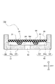
- FIG. 27 is a view for explaining the current measurement device 900 disclosed in Patent Document 1, and is a cross-sectional view showing the positional relationship between the magnetic sensor 910 and the conductor 901 to be measured.
- the current measuring device 900 is configured of a conductor to be measured 901 formed on a printed circuit board 911 and a magnetic sensor 910 (having a magnetic detection element inside) mounted on the printed circuit board 912.
- the magnetic sensor 910 detects a magnetic field 920 generated in the width direction of the conductor 901 when the current to be measured flows through the conductor 901.
- the frequency of the current to be measured flowing in such a flat shaped conductor to be measured 901 becomes high, the current to be measured is concentrated on the end of the conductor to be measured 901 by the skin effect, and the center of the conductor 901 to be measured Then, the current density decreases, and the current density increases near the end of the conductor 901 to be measured. Therefore, when the magnetic sensor 910 is disposed at the center of the conductor to be measured 901 (located at the end in FIG. 27), the magnetic field 920 near the center detected by the magnetic sensor 910 decreases and the current sensitivity of the current measuring device 900 There was a problem to say that it falls.
- the magnetic sensor 910 is provided at a position separated by a predetermined distance from the central position CL in the width direction of the conductor 901 to be measured. As a result, it is possible to provide the current measurement apparatus 900 in which the decrease in measurement sensitivity is suppressed even in the case of a high-frequency measurement current.
- the magnetic sensor 910 is disposed near the end of the conductor 901 to be measured in accordance with the frequency of the current to be measured, the same applies to other devices using the current to be measured having different frequencies.
- the frequency changes depending on the state even with an apparatus the current sensitivity measured by the current measuring device 900 is largely different, and there is a problem that accurate measurement accuracy can not be obtained.
- the case where the frequency of the current to be measured changes depending on the state is, for example, a case where the frequency of the current to be measured changes depending on states such as idling, acceleration and regenerative braking in an electric car or a hybrid car. Be
- the present invention solves the above-mentioned problem, and an object of the present invention is to provide a current sensor that can perform measurement with high accuracy even if the frequency of the current to be measured changes.
- the current sensor includes a first current path having a first flat portion and a measured current which is disposed on the first current path and flows in the first current path. And a first magnetoelectric conversion element for detecting magnetism generated in the first current path, wherein the first current path is connected to the first current path.
- a lowest frequency magnetic flux density which is a magnetic flux density in the case of flowing the measured current of the lowest frequency used in the device, provided with a conductive first convex portion along the direction in which the current flows;
- the first magnetoelectric conversion element is disposed at a position on the first current path where the maximum frequency magnetic flux density, which is the magnetic flux density in the case of flowing the measured current of the highest frequency to be used, substantially matches It is characterized.
- the target of the lowest frequency used in the device is The lowest frequency magnetic flux density, which is the magnetic flux density when the measurement current flows, and the highest frequency magnetic flux density, which is the magnetic flux density when the highest frequency of the measured current flows, can be made closer to each other. Therefore, the first magnetoelectric conversion element can be disposed at a position where the change in magnetic flux density due to the change in frequency is small. As a result, even if the frequency of the current to be measured changes, the lowest frequency magnetic flux density and the highest frequency magnetic flux density do not differ significantly, so that the current value can be measured accurately.
- the current sensor of the present invention is characterized in that the first convex portion is erected from any one end of the first flat portion.
- the first magnetoelectric conversion element can be disposed closer to the center of the first current path, and the magnetic sensor (magnetoelectric conversion element) 910 is disposed outside the measured conductor (current path) 901 as in the conventional example.
- the influence of the external magnetic field from the adjacent current paths and the like can be reduced as compared with the case where
- the first flat portion and the first convex portion are integrally formed by bending a metal plate.
- a second current path having a second flat portion and a magnetism generated when the current to be measured is disposed on the second current path and flows in the second current path.
- a connecting portion for connecting one ends of the first current path and the second current path to each other, and the first current path and the second current path are connected in parallel
- the other end of the second current path is connected to the device, and the second current path is provided with a conductive second convex portion along the direction in which the current to be measured flows.
- the lowest frequency magnetic flux density which is the magnetic flux density when the measured current of the lowest frequency used in the device flows, and the highest frequency, the magnetic flux density when the measured current of the highest frequency used in the device flows
- the second current path substantially matching the magnetic flux density
- the second magnetoelectric conversion element is disposed at the position of the first convex portion, and the first convex portion is erected from the end portion on the side away from the second current path, and the second convex portion
- the first magnetoelectric conversion element and the second magnetoelectric conversion element are provided on the same substrate, and the first magnetoelectric conversion element and the second magnetoelectric conversion element are provided on the same substrate.
- the second magnetoelectric conversion element can be disposed at a position where the change in magnetic flux density due to the change in frequency is small. As a result, even if the frequency of the current to be measured changes, the lowest frequency magnetic flux density and the highest frequency magnetic flux density do not greatly differ, so that the current value can be measured with high accuracy also in the second current path.
- the first magnetoelectric conversion element and the second magnetoelectric conversion element are respectively provided on the same substrate, when current flows in the external magnetic field or the current path (the first current path and the second current path) The influence of the generated internal magnetic field appears with the same strength in the two magnetoelectric transducers (the first magnetoelectric transducer and the second magnetoelectric transducer). Therefore, by differentially processing the outputs from the two magnetoelectric conversion elements (the first magnetoelectric conversion element and the second magnetoelectric conversion element), the influence of the magnetic field can be canceled more accurately. This can reduce the deterioration of the measurement accuracy of the current sensor.
- the current sensor of the present invention has at least two or more of the first magnetoelectric conversion elements and at least two of the second magnetoelectric conversion elements, and at least one of the first magnetoelectric conversion elements is the first one.
- the first flat shape in which at least one of the first magnetoelectric conversion elements is not provided while the first convex portion is disposed at the first position of the first flat portion on which the convex portion is provided.
- a third position of the second portion, and at least one of the second magnetoelectric conversion elements is disposed at a second position of the second flat-shaped portion on which the second convex portion is erected; It is characterized in that at least one of the two magnetoelectric conversion elements is disposed at a fourth position of the second flat portion where the second convex portion is not provided.
- the first magnetoelectric conversion element disposed at the first position of the first current path where the first convex portion is erected and the second position of the second current path where the second convex portion is erected And the second magnetoelectric conversion element, and the third position of the first current path where the first convex portion is not erected and the first magnetoelectric conversion provided at the fourth position of the second current path where the second convex portion is not erected
- the element and the second magnetoelectric conversion element are separately disposed.
- the magnetic amounts detected by the first magnetoelectric conversion element and the second magnetoelectric conversion element disposed at the first position and the second position, and the first magnetoelectric conversion element disposed at the third position and the fourth position The absolute amount of the amount of magnetism detected by the second magnetoelectric conversion element differs. Therefore, the first magnetoelectric conversion element and the second magnetoelectric conversion element disposed at the first position and the second position are disposed at the third position and the fourth position for high current measurement, and The second magnetoelectric conversion element can be used separately for constant current measurement. As a result, in the case of high current measurement, measurement can be performed in a wide range, and in the case of low current measurement, measurement can be performed with high accuracy.
- the first flat portion, the first convex portion, the connection portion, the second flat portion and the second convex portion are integrally formed by bending a metal plate. It is characterized by
- the first current path is provided with the conductive first convex portion that is long along the direction in which the current to be measured flows, the lowest frequency used in the device (the device to be measured)
- the lowest frequency magnetic flux density which is the magnetic flux density when the current to be measured flows
- the highest frequency magnetic flux density which is the magnetic flux density when the current to be measured at the highest frequency flows
- the first magnetoelectric conversion element can be disposed at a position where the change in magnetic flux density due to the change in frequency is small.
- FIG. 18A is a cross-sectional view taken along line XVII-XVII shown in FIG. 17
- FIG. 18B is a block diagram illustrating the current sensor of the third embodiment of the present invention. It is a cross-sectional view taken along line XVIII-XVIII. It is a top view of the 1st current course of the model used for simulation of the current sensor of a 3rd embodiment of the present invention, the 2nd current course, and a connection part.
- FIG. 22 (a) is a simulation result in the direction of XX-XX line shown in FIG. 19 in the current sensor of the third embodiment of the present invention, and FIG. It is a simulation result of the comparative example compared with a).
- FIG. 22 (a) is a simulation result in the direction of XX-XX line shown in FIG. 19 in the current sensor of the third embodiment of the present invention, and FIG. It is a simulation result of the comparative example compared with a).
- FIG. 23 is a view for explaining a modification of the current sensor according to the first embodiment of the present invention, and FIG. 23 (a) is a model of Modification 1, and FIG. 23 (b) is a model of Modification 2; 23 (c) is a model diagram of the third modification, and FIG. 23 (d) is a model diagram of the fourth modification. It is a figure explaining the modification of the current sensor of a 1st embodiment of the present invention, and Drawing 24 (a) is a top view of modification 5; Drawing 24 (b) is a top view of modification 6 It is.
- FIG.25 (a) is a perspective view of the modification 7
- FIG.25 (b) is a perspective of the modification 8.
- FIG. 25 (c) is a perspective view of Modification 9
- FIG. FIG. 26A is a view comparing with a current sensor according to an embodiment of the present invention
- FIG. 26A is a view of a model H101 of a comparative example used for the simulation
- FIG. 26B is a simulation of the model H101. It is a graph of a result.
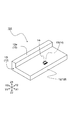
- FIG. 1 is an exploded perspective view for explaining a current sensor 101 according to a first embodiment of the present invention.
- FIG. 2 is a perspective view for explaining the current sensor 101 according to the first embodiment of the present invention.
- the insulating substrate 19 is omitted to facilitate the description.
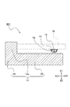
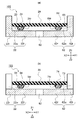
- FIG. 3 is a configuration diagram for explaining the current sensor 101 according to the first embodiment of the present invention, and is a top view seen from the Z1 side shown in FIG.
- FIG. 4 is a configuration diagram for explaining the current sensor 101 according to the first embodiment of the present invention, and is a cross-sectional view taken along the line IV-IV shown in FIG.
- the current sensor 101 includes a first current path 12 having a first flat portion 12f, and a first current path 12 disposed on the first current path 12.
- a magnetoelectric conversion element 13 is provided.
- the insulating substrate 19 disposed opposite to the first current path 12 and, although not shown, external control for supplying power to the current sensor 101 and for taking out a signal from the current sensor 101.
- a connector is provided to connect to the device.
- the first current path 12 is made of a metal material having good conductivity such as copper (Cu), and as shown in FIGS. 1 to 4, a first flat portion 12 f and one of the first current paths 12.
- the first projection 12w is configured to have a first projection 12w erected from the end 12t, and the first projection 12w is formed along the flow direction of the current to be measured (Y direction shown in FIG. 2). There is. Further, although not shown, at both ends of the first current path 12, holding portions for connecting and fixing a current path to be measured (a current path to be measured) of a device (device to be measured) not shown. It is provided.
- the first flat portion 12 f and the first convex portion 12 w are integrally formed by bending a metal plate such as copper (Cu). Thereby, when manufacturing the 1st flat part 12f and the 1st convex part 12w, it can manufacture easily from one metal plate. By this, the current sensor 101 can be made inexpensive.
- the first magnetoelectric conversion element 13 is an element for detecting the magnetism generated when the current to be measured flows in the first current path 12 and is, for example, a magnetoresistance effect element (GMR (Giant) using a giant magnetoresistance effect. It is packaged in the magnetic sensor package 14 as shown in FIG. 4 using a Magneto Resistive) element. Further, as shown in FIGS. 2 and 3, the first magnetoelectric conversion element 13 is disposed on the first flat portion 12 f and disposed near the center of the first flat portion 12 f in the longitudinal direction. And the other end of the first current path 12. The sensitivity direction of the first magnetoelectric transducer 13 is disposed in the X direction shown in FIG.
- GMR magnetoresistance effect element
- the magnetic sensor package 14 is fabricated of a GMR element formed on a silicon substrate, and then electrically connected to a chip of the GMR element cut out and a lead terminal 14r for taking out a signal, and a thermosetting synthetic resin. Packaged and manufactured.
- the magnetic sensor package 14 is soldered to the insulating substrate 19 which is a circuit substrate by the lead terminals 14r, and is connected to an external control device via a wiring pattern and a connector (not shown).
- the first magnetoelectric conversion element 13 is packaged and disposed on the insulating substrate 19 as the magnetic sensor package 14, for example, the first magnetoelectric conversion element 13 may be disposed as it is, so-called bare chip mounting. good.
- the insulating substrate 19 uses a widely known single-sided printed wiring board, and a metal foil such as copper (Cu) provided on the base substrate is patterned on a glass-filled epoxy resin base substrate. , Forming a wiring pattern.
- a metal foil such as copper (Cu) provided on the base substrate is patterned on a glass-filled epoxy resin base substrate. , Forming a wiring pattern.
- one magnetic sensor package 14 in which the first magnetoelectric transducer 13 is packaged is mounted on the insulating substrate 19.
- a printed wiring board made of an epoxy resin containing glass is used as the insulating substrate 19, the present invention is not limited to this.
- a ceramic wiring board or a flexible wiring board may be used.
- a circuit board is preferably used as the insulating board 19.
- the present invention is not limited to the circuit board, and the magnetic sensor package 14 is mounted by overlapping the circuit board on the insulating board 19. It may be configured to
- FIG. 5 is a cross-sectional view of the first current path 12 of the model used for the simulation of the current sensor of the first embodiment of the present invention
- FIG. 5 (a) is a model A1
- 6 is a cross-sectional view of the first current path 12 of the model used in the simulation of the current sensor according to the first embodiment of the present invention
- FIG. 6 (a) is a model B1.
- b) is model B2.
- the numerical values used for this simulation (see FIGS. 5 and 6) set the entire length of the first current path 12 to 100 (mm), the entire width W 1 to 20 (mm), and the first flat portion 12f.
- the thickness T1 of each of the models was 4 (mm), and the length of the first convex portion 12 w was 100 (mm).
- the width W2 of the first protrusion 12w is 4 (mm), the thickness T2 is 4 (mm), and for the model A2, the width W2 of the first protrusion 12w is 4 (mm), and the thickness T2 is In the model B1, the width W2 of the first convex portion 12w is 6 (mm), the thickness T2 is 4 (mm), the width W2 of the first convex portion 12w is 8 (mm), and the thickness T2 of the model B1. It was 4 (mm) and was made variable.
- the current sensor 101 shown in FIGS. 1 to 4 is an embodiment of the model A1.
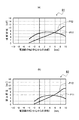
- FIG. 7 is a simulation result of the current sensor according to the first embodiment of the present invention, which is a graph corresponding to the model A1 of FIG. 5A and the model A2 of FIG. 5B.
- FIG. 8 is a simulation result of the current sensor according to the first embodiment of the present invention, which is a graph corresponding to the model B1 of FIG. 6A and the model B2 of FIG. 6B.
- the horizontal axes of the graphs in FIGS. 7 and 8 represent the width W1 of the first current path 12 and indicate the distances from the center (10 (mm) respectively on the left and right), and the vertical axes in the graphs in FIGS.
- P11 in the figure indicates the lowest frequency magnetic flux density when the frequency of the current to be measured used in the device (device to be measured) is 10 (Hz) and the lowest frequency assumed
- P2 in the figure is The frequency of the measured current used in the device (device to be measured) is 10 (kHz), which indicates the highest frequency magnetic flux density in the case of the highest frequency assumed.
- FIG. 26 is a view comparing with the current sensor 101 according to the first embodiment of the present invention
- FIG. 26 (a) is a view of a model H101 of a comparative example used for the simulation; These are graphs of the simulation result of the model H101.
- the length of the current path H12 was 100 (mm)
- the thickness H1 was 4 (mm)
- the width H2 was 20 (mm).
- the first convex is compared with the case where the magnetic flux density largely differs due to the difference between the low frequency and the high frequency of the current to be measured as shown in FIG.
- the difference between the magnetic flux density due to the difference between the low frequency and the high frequency of the current to be measured that is, the difference between the lowest frequency magnetic flux density P11 and the highest frequency magnetic flux density P2 on the first flat portion 12f not provided with the portion 12w It was getting smaller. This is considered to be because the magnetic field around the first current path 12 was changed by providing the first convex portion 12 w. Therefore, the lowest frequency magnetic flux density P11 and the highest frequency magnetic flux density P2 can be made closer to each other by providing the conductive first convex portion 12w along the direction in which the current to be measured flows, and can be made more consistent.
- the first magnetoelectric conversion element 13 be disposed at a position on the first current path 12 where the lowest frequency magnetic flux density P11 and the highest frequency magnetic flux density P2 substantially match.
- the distance from the center is approximately 7 (mm) on the first flat portion 12f where the first convex portion 12w of the first current path 12 is not provided.
- the first magnetoelectric conversion element 13 is disposed at a distance of about 6.5 (mm).
- the distance from the center is about 5.5 (on the first flat portion 12 f where the first convex portion 12 w of the first current path 12 is not provided). It is desirable to arrange the first magnetoelectric conversion element 13 at the position of mm), and in the case of the model B2, on the first flat portion 12f where the first convex portion 12w of the first current path 12 is not provided, It is desirable to arrange the first magnetoelectric conversion element 13 at a distance of about 5 (mm) from the center.
- the first magnetoelectric conversion element 13 can be disposed at a position where the change in magnetic flux density due to the change in frequency is small. Since the lowest frequency magnetic flux density P11 and the highest frequency magnetic flux density P2 do not differ greatly, it is possible to measure the current value accurately.
- the current measuring device 900 of the conventional example the position (the R portion of the peak of the highest frequency magnetic flux density P2 shown in FIG. 26B) shown in FIG. Since the magnetic sensor 910 is provided at a distance of about 9 (mm), the difference between the lowest frequency magnetic flux density P11 and the highest frequency magnetic flux density P2 is large. Therefore, when applied to another device using a measured current having a different frequency or when the frequency changes depending on the state even with the same device, the current sensitivity measured by the current measuring device 900 is largely different, and accurate measurement The accuracy can not be obtained.
- the first convex portion 12w is erected from the end 12t of the first flat portion 12f, and the height T2 and the width W2 of the first convex portion 12w are changed.
- the position where the change of the magnetic flux density accompanying the frequency change is small can be arbitrarily changed.
- the arrangement position of the 1st magnetoelectric conversion element 13 can also be set up arbitrarily.
- the position where the change in the magnetic flux density accompanying the change in the frequency is small can be changed by changing the shape of the first convex portion 12w, for example, the length or the surface shape of the corner,
- the arrangement position of the 1 magnetoelectric transducer 13 can be set arbitrarily.
- the first convex portion 12w is erected from the end 12t of the first flat portion 12f, the lowest frequency magnetic flux density P11 and the highest frequency magnetic flux density P2 are approximately The coincident position can be moved to the center side of the first current path 12.
- the first magnetoelectric conversion element 13 can be disposed closer to the center of the first current path 12 and the magnetic sensor (magnetoelectric conversion element) 910 is provided outside the measured conductor (current path) 901 as in the conventional example.
- the influence of the external magnetic field from the adjacent current paths and the like can be reduced as compared with the case where the
- the existence of this effect can solve the following problems.
- By changing the height H2 and the width W2 of the first convex portion 12w it is possible to arbitrarily change the position where the lowest frequency magnetic flux density P11 and the highest frequency magnetic flux density P2 substantially coincide with each other.
- the position where the sensor can be arranged is limited, and the current measuring device 900 as in the conventional example can solve the problem that the magnetic sensor (magnetoelectric conversion element) 910 can not be arranged at the best position.
- the first magnetoelectric conversion element 13 be disposed at a position on the first current path 12 at which the lowest frequency magnetic flux density P11 and the highest frequency magnetic flux density P2 substantially match, the lowest frequency magnetic flux density
- the first magnetoelectric conversion element 13 may be disposed at a position on the first current path 12 corresponding to a region where P11 and the maximum frequency magnetic flux density P2 become equal.
- a region where the lowest frequency magnetic flux density P11 and the highest frequency magnetic flux density P2 are equal that is, the distance from the center is 4.5 (mm) to 7
- the first magnetoelectric conversion element 13 may be disposed between 5 mm and preferably between 5.5 mm and 7 mm.
- the distance from the center is between 2.5 (mm) and 7 (mm), preferably 4.5 (mm) to 6 (mm)
- the first magnetoelectric conversion element 13 may be disposed between them.
- the first convex portion 12 w can be provided so that the region in which the lowest frequency magnetic flux density P 11 and the highest frequency magnetic flux density P 2 are equal becomes wide.
- the first magnetoelectric conversion element 13 can be disposed arbitrarily within the range of this region, so that, for example, even in the case where the position where the current sensor 101 can be disposed is limited in the on-vehicle application, the first The magnetoelectric conversion element 13 can be disposed at the best position.
- the first current path 12 is provided with the conductive first convex portion 12 w which is long along the flowing direction of the current to be measured.
- the lowest frequency magnetic flux density P11 which is the magnetic flux density in the case of flowing the measured current of the lowest frequency used in the device
- the highest frequency magnetic flux density P2 which is the magnetic flux density in the case of flowing the measured current of the highest frequency
- the first convex portion 12w is erected from one end 12t of the first flat portion 12f, a position where the lowest frequency magnetic flux density P11 and the highest frequency magnetic flux density P2 substantially coincide with each other is It can be moved to the center side of the current path 12.
- the first magnetoelectric conversion element 13 can be disposed closer to the center of the first current path 12 and the magnetic sensor (magnetoelectric conversion element) 910 is provided outside the measured conductor (current path) 901 as in the conventional example.
- the influence of the external magnetic field from the adjacent current paths and the like can be reduced as compared with the case where the
- first flat portion 12f and the first convex portion 12w are integrally formed by bending a metal plate, one sheet of the first flat portion 12f and the first convex portion 12w can be manufactured. It can be easily manufactured from the metal plate of By this, the current sensor 101 can be made inexpensive.
- FIG. 9 is an exploded perspective view for explaining the current sensor 102 according to the second embodiment of the present invention.
- FIG. 10 is a perspective view for explaining the current sensor 102 according to the second embodiment of the present invention.
- FIG. 11 is a configuration diagram for explaining the current sensor 102 according to the second embodiment of the present invention, and is a top view seen from the Z1 side shown in FIG.
- FIGS. 10 and 11 show the substrate 29 in a transparent state for ease of explanation.
- FIG. 12 is a configuration diagram for explaining the current sensor 102 according to the second embodiment of the present invention, and is a cross-sectional view taken along line XII-XII shown in FIG.
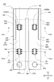
- the current sensor 102 of the second embodiment differs from the first embodiment in that the second current path 62 and the second magnetoelectric conversion element 63 are provided.
- the same composition as a 1st embodiment the same numerals are attached and detailed explanation is omitted.
- the current sensor 102 has a first current path 22 having a first flat portion 22f and a second current path having a second flat portion 62f, as shown in FIGS. 62, a connection portion 92 connecting one ends of the first current path 22 and the second current path 62, a first magnetoelectric conversion element 23 disposed on the first current path 22, and a second current path 62 And a second magnetoelectric conversion element 63 disposed on the upper side.
- a substrate 29 disposed opposite to the first current path 22 and the second current path 62, and although not shown, for supplying power to the current sensor 102 and for taking out a signal from the current sensor 102.
- a connector is provided in order to connect to an external control device.
- the first current path 22 is made of a metal material with good conductivity such as copper (Cu), and as shown in FIGS. 9 to 12, a first flat portion 22f and one of the first current paths 22.
- the first convex portion 22 w is provided with a first convex portion 22 w standing from the end portion 22 t, and the first convex portion 22 w is formed along the flow direction of the current to be measured (Y direction shown in FIG. 10) There is.
- a terminal portion 27A is provided on the other end side of the first current path 22 continuously to the first current path 22, and the terminal portion 27A is illustrated.
- a through hole 27h is provided for connecting and fixing the measured current path (current path to be measured) of a non-apparatus (device to be measured).
- the second current path 62 is made of a conductive metal material such as copper (Cu), and as shown in FIGS. 9 to 12, a second flat portion 62f and one of the second current paths 62.
- the second convex portion 62w is provided with a second convex portion 62w standing from the end portion 62t, and the second convex portion 62w is formed along the flow direction of the current to be measured (Y direction shown in FIG. 10). There is.
- a terminal portion 27B is provided continuously to the second current path 62 on the other end side of the second current path 62, and the terminal portion 27B is illustrated. There is provided a through hole 27k for connecting and fixing a current path to be measured (a current path to be measured) of a device (device to be measured).
- the first current path 22 and the second current path 62 are arranged in parallel, as shown in FIGS. 9 to 11, and one end of each is connected by a connection portion 92.
- the first convex portion 22 w of the first current path 22 is erected from the end 22 t on the side away from the second current path 62
- the second convex portion 62 w of the second current path 62 is the first It is disposed to stand from an end 22t remote from the current path 22.
- the 1st convex part 22w and the 2nd convex part 62w are arrange
- the first current path 22, the second current path 62, and the connection portion 92 are U-shaped, and the first current path 22 and the second current path 62 are It is line symmetrical.
- first flat portion 22f, the first convex portion 22w, the connection portion 92, the second flat portion 62f, and the second convex portion 62w described above integrally bend a metal plate such as copper (Cu). It is formed.
- a metal plate such as copper (Cu).
- the first magnetoelectric conversion element 23 is an element for detecting the magnetism generated when the current to be measured flows in the first current path 22.
- the first magnetoelectric conversion element 23 is a magnetoresistance effect element using a giant magnetoresistance effect (GMR (Giant It is packaged in the magnetic sensor package 24 as shown in FIG. 12 using a Magneto Resistive) element.
- GMR giant magnetoresistance effect
- the first magnetoelectric conversion element 23 is disposed on the first flat portion 22f of the portion where the first convex portion 22w is erected.
- the sensitivity direction of the first magnetoelectric transducer 23 is disposed in the X direction shown in FIG.
- the second magnetoelectric conversion element 63 is an element for detecting the magnetism generated when the current to be measured flows in the second current path 62 and, like the first magnetoelectric conversion element 23, for example, the giant magnetoresistance effect
- the magnetoresistive effect element (referred to as a GMR (Giant Magneto Resistive) element) used is packaged in a magnetic sensor package 64 as shown in FIG.
- the second magnetoelectric conversion element 63 is disposed on the second flat portion 62f of the portion where the second convex portion 62w is provided.
- the sensitivity direction of the second magnetoelectric transducer 63 is disposed in the X direction shown in FIG. Since differential processing is performed between the first magnetoelectric conversion element 23 and the second magnetoelectric conversion element 63, the sensitivity axes of the first magnetoelectric conversion element 23 and the second magnetoelectric conversion element 63 are in the same direction. It is arranged as
- the magnetic sensor package (24, 64) described above electrically connects the chip of the GMR element cut out to the lead terminal (24r, 64r) for signal extraction after the GMR element is fabricated on a silicon substrate It is manufactured by packaging with a thermosetting synthetic resin.
- the magnetic sensor package 24 and the magnetic sensor package 64 are provided on the same substrate 29 by being soldered to a substrate 29 which is a circuit substrate by lead terminals (24 r, 64 r).
- the magnetic sensor package 24 and the magnetic sensor package 64 are connected to an external control device via a wiring pattern and a connector (not shown).
- first magnetoelectric conversion element 23 and the second magnetoelectric conversion element 63 are packaged and disposed on the substrate 29 as the magnetic sensor package (24, 64), for example, the first magnetoelectric conversion element 23 and the second magnetoelectric conversion The element 63 may be disposed as it is, so-called bare chip mounting, and disposed on the same substrate 29.
- the substrate 29 uses a widely known double-sided printed wiring board, and a metal foil such as copper (Cu) provided on a base substrate is patterned on a glass-filled epoxy resin base substrate, A wiring pattern is formed.
- a metal foil such as copper (Cu) provided on a base substrate is patterned on a glass-filled epoxy resin base substrate, A wiring pattern is formed.
- one magnetic sensor package (4, 64) in which the first magnetoelectric conversion element 23 and the second magnetoelectric conversion element 63 are packaged is mounted on the substrate 29. It has become.
- a printed wiring board made of epoxy resin containing glass is used as the substrate 29, the present invention is not limited to this.
- a ceramic wiring board or a flexible wiring board may be used.
- a circuit board is preferably used as the board 29.
- the present invention is not limited to the circuit board, and the magnetic sensor package (24, 64) is obtained by superposing the circuit board on the board 29. May be mounted.
- FIG. 13 is a cross-sectional view of the first current path 22 and the second current path 62 of the model C1 used for the simulation of the current sensor of the second embodiment of the present invention.
- the numerical values used for this simulation set the entire length of the first current path 22 to 100 (mm), the entire width W21 to 20 (mm), and the thickness T21 of the first flat portion 22f.
- the length of the first convex portion 22w is 60 (mm), the width W22 is 4 (mm), and the height T22 is 10 (mm).
- the overall length of the second current path 62 is 100 (mm), the overall width W 61 is 20 (mm), and the thickness T 61 of the second flat portion 62 f is 4 (mm).
- the length was 60 (mm), the width W 62 was 4 (mm), and the height T 62 was 10 (mm).
- the distance W41 between the first current path 22 and the second current path 62 is 5 (mm).
- the magnetic flux density in a space 1 mm away from the surface of the first current path 22 and the second current path 62 was used.
- the current sensor 102 shown in FIGS. 9 to 12 is an embodiment of the model C1.
- FIG. 14 is a simulation result of the model C1 of the current sensor of the second embodiment of the present invention.
- the horizontal axis of the graph in FIG. 14 indicates the distance in the width direction when the midpoint between the first current path 22 and the second current path 62 is zero, and the negative side is the first current path 22 and the positive side is the second. It is the current path 62.
- the vertical axis of the graph of FIG. 14 indicates the magnetic flux density in a portion where the first convex portion 22 w of the first flat portion 22 f and the second convex portion 62 w of the second flat portion 62 f are not provided.
- P21 in the figure indicates the lowest frequency magnetic flux density when the frequency of the current to be measured used in the device (device to be measured) is 10 (Hz) and the lowest frequency assumed
- P22 in the figure is The frequency of the measured current used in the device (device to be measured) is 10 (kHz), which indicates the highest frequency magnetic flux density in the case of the highest frequency assumed.
- the low frequency and the high frequency of the current to be measured are on the second flat portion 62f where the second convex portion 62w is not provided.
- the difference in magnetic flux density due to the difference between the two that is, the difference between the lowest frequency magnetic flux density P21 and the highest frequency magnetic flux density P22 is small. It is considered that this is because the magnetic field around the second current path 62 was changed by providing the second convex portion 62 w. Therefore, the lowest frequency magnetic flux density P21 and the highest frequency magnetic flux density P22 can be made closer to each other by providing the conductive second convex portion 62w along the flowing direction of the current to be measured, and can be made to more coincide with each other.
- the first magnetoelectric conversion element 23 and the second magnetoelectric conversion element are provided at positions above the first current path 22 and the second current path 62 where the lowest frequency magnetic flux density P21 and the highest frequency magnetic flux density P22 substantially match.
- 63 are provided.
- the distance from the center is about ⁇ 7.5 (on the first flat portion 22f where the first convex portion 22w of the first current path 22 is not provided).
- the first magnetoelectric conversion element 23 It is desirable to dispose the first magnetoelectric conversion element 23 at a position of about 5 (mm) from the other end of the first current path 22, and the second convex portion 62 w of the second current path 62 is provided The second magnetoelectric conversion element at a distance of about 7.5 (mm) ⁇ about 5 (mm) from the other end of the second current path 62 ⁇ on the second flat portion 62f which is not It is desirable to arrange 63.
- the first magnetoelectric conversion element 23 and the second magnetoelectric conversion element 63 can be disposed at a position where the change in magnetic flux density due to the frequency change is small. Since the lowest frequency magnetic flux density P ⁇ b> 21 and the highest frequency magnetic flux density P ⁇ b> 22 do not greatly differ even if the frequency of [1] changes, the current value can be measured accurately.
- the first magnetoelectric conversion element 23 and the second magnetoelectric conversion element 63 are provided on the same substrate 29 respectively, the current in the external magnetic field or the current path (the first current path 22 and the second current path 62) The influence by the internal magnetic field generated when the magnetic flux flows appears with the same strength in the two magnetoelectric conversion elements (the first magnetoelectric conversion element 23 and the second magnetoelectric conversion element 63). Therefore, by differentially processing the outputs from the two magnetoelectric conversion elements (the first magnetoelectric conversion element 23 and the second magnetoelectric conversion element 63), the influence of the magnetic field can be offset more accurately. By this, the deterioration of the measurement accuracy of the current sensor 102 can be reduced.
- the position where the change of the magnetic flux density accompanying the frequency change is small It can be changed arbitrarily.
- positioning position of the 1st desired magnetoelectric conversion element 23 can also be set arbitrarily.
- the position at which the change in the magnetic flux density accompanying the change in the frequency is small can be arbitrarily changed by changing the shape of the first convex portion 22w, for example, the length or the surface shape of the corner. .
- the first magnetoelectric conversion element 23 be disposed at a position on the first current path 22 where the lowest frequency magnetic flux density P21 and the highest frequency magnetic flux density P22 substantially match, the lowest frequency magnetic flux density
- the first magnetoelectric conversion element 23 may be disposed at a position on the first current path 22 corresponding to a region where P21 and the maximum frequency magnetic flux density P22 become equal.
- a region where the lowest frequency magnetic flux density P21 and the highest frequency magnetic flux density P22 are equal ie, the distance from the center is -6 (mm)
- the first magnetoelectric conversion element 23 may be disposed between 14 (mm), preferably between -7 (mm) and -9 (mm).
- the distance from the center is between 6 (mm) and 14 (mm), preferably between 7 (mm) and 9 (mm)
- the second magnetoelectric conversion element 63 may be disposed.
- the first convex portion 22 w and the second convex portion 62 w can be provided so that the region where the lowest frequency magnetic flux density P 21 and the highest frequency magnetic flux density P 22 are equal is wide.
- the first magnetoelectric conversion element 23 and the second magnetoelectric conversion element 63 can be disposed arbitrarily within the range of this region, for example, when the position where the current sensor 102 can be disposed is limited in an on-vehicle application Even if it is, the 1st magnetoelectric conversion element 23 and the 2nd magnetoelectric conversion element 63 can be arranged in the best position.
- the first current path 22 is provided with the conductive first convex portion 22 w which is long along the flowing direction of the current to be measured.
- the lowest frequency magnetic flux density P21 which is the magnetic flux density when the measured current of the lowest frequency used in the instrument
- the highest frequency magnetic flux density P22 which is the magnetic flux density when the measured current of the highest frequency flows. It can be closely matched more closely. Therefore, the first magnetoelectric conversion element 23 can be disposed at a position where the change in magnetic flux density due to the change in frequency is small. As a result, even if the frequency of the current to be measured changes, the lowest frequency magnetic flux density P21 and the highest frequency magnetic flux density P22 do not greatly differ, so that the current value can be measured accurately.
- the second current path 62 is provided with the conductive second convex portion 62w along the flowing direction of the current to be measured, the magnetic flux in the case of flowing the current to be measured of the lowest frequency used in the device.
- the lowest frequency magnetic flux density P21 which is the density
- the highest frequency magnetic flux density P22 which is the magnetic flux density in the case where the current to be measured at the highest frequency is supplied, can be made closer to each other.
- the second magnetoelectric conversion element 63 can be disposed at a position where the change in magnetic flux density due to the change in frequency is small.
- the lowest frequency magnetic flux density P21 and the highest frequency magnetic flux density P22 do not greatly differ, so that the current value can be measured accurately also in the second current path 62.
- the first magnetoelectric conversion element 23 and the second magnetoelectric conversion element 63 are provided on the same substrate 29 respectively, the current in the external magnetic field or the current path (the first current path 22 and the second current path 62) The influence by the internal magnetic field generated when the magnetic flux flows appears with the same strength in the two magnetoelectric conversion elements (the first magnetoelectric conversion element 23 and the second magnetoelectric conversion element 63). Therefore, by differentially processing the outputs from the two magnetoelectric conversion elements (the first magnetoelectric conversion element 23 and the second magnetoelectric conversion element 63), the influence of the magnetic field can be offset more accurately. By this, the deterioration of the measurement accuracy of the current sensor 102 can be reduced.
- first flat portion 22f, the first convex portion 22w, the connection portion 92, the second flat portion 62f, and the second convex portion 62w are integrally formed by bending a metal plate such as copper (Cu).
- a metal plate such as copper (Cu).
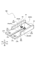
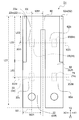
- FIG. 15 is an exploded perspective view for explaining the current sensor 103 according to the third embodiment of the present invention.
- FIG. 16 is a perspective view for explaining the current sensor 103 according to the third embodiment of the present invention.
- FIG. 17 is a configuration diagram for explaining the current sensor 103 according to the third embodiment of the present invention, and is a top view seen from the Z1 side shown in FIG.
- FIGS. 16 and 17 show the substrate 29 in a transparent state for ease of explanation.
- FIG. 18 is a configuration diagram for explaining a current sensor 103 according to a third embodiment of the present invention, and FIG. 18 (a) is a cross-sectional view along line XVII-XVII shown in FIG.
- the current sensor 103 according to the third embodiment is different from the second embodiment in that the first magnetoelectric conversion element 33 and the second magnetoelectric conversion element 73 are provided.
- the same composition as a 1st embodiment and a 2nd embodiment the same numerals are attached and detailed explanation is omitted.
- the current sensor 103 has a first current path 22 having a first flat portion 22f and a second current path having a second flat portion 62f, as shown in FIGS. 62, a connection portion 92 connecting one ends of the first current path 22 and the second current path 62, and a first magnetoelectric conversion element 23 and a first magnetoelectric conversion element 33 disposed on the first current path 22. , And a second magnetoelectric conversion element 63 and a second magnetoelectric conversion element 73 disposed on the second current path 62.
- the substrate 29 disposed opposite to the first current path 22 and the second current path 62, and although not shown, for supplying power to the current sensor 103 and for taking out a signal from the current sensor 103.
- a connector is provided in order to connect to an external control device.
- the first current path 22, the second current path 62, and the connection portion 92 have the same structure as in the second embodiment, and thus the description thereof will be omitted.
- the first magnetoelectric conversion element 23 is disposed on the first position 22a of the first flat portion 22f on which the first convex portion 22w is provided.
- the sensitivity direction of the first magnetoelectric transducer 23 is disposed in the X direction shown in FIG.
- the first magnetoelectric conversion element 33 is an element for detecting the magnetism generated when the current to be measured flows in the first current path 22.
- the first magnetoelectric conversion element 33 is a magnetoresistance effect element using a giant magnetoresistance effect (GMR (Giant It is packaged in a magnetic sensor package 34 as shown in FIG. 18 using a Magneto Resistive) element.
- GMR giant magnetoresistance effect
- the first magnetoelectric conversion element 33 is disposed on the third position 22c of the first flat portion 22f in which the first convex portion 22w is not provided.
- the sensitivity direction of the first magnetoelectric conversion element 33 is disposed so as to be the X direction shown in FIG. 17 so that the same sensitivity axis as the first magnetoelectric conversion element 23 is directed.
- the second magnetoelectric conversion element 63 is disposed on the second position 62b of the second flat portion 62f on which the second convex portion 62w is provided.
- the sensitivity direction of the second magnetoelectric transducer 63 is disposed in the X direction shown in FIG.
- the second magnetoelectric conversion element 73 is an element for detecting the magnetism generated when the current to be measured flows in the second current path 62, and, for example, a magnetoresistance effect element (GMR (Giant) using a giant magnetoresistance effect. It is packaged in a magnetic sensor package 74 as shown in FIG. In addition, as shown in FIGS. 16 and 17, the second magnetoelectric conversion element 73 is disposed on the fourth position 62d of the second flat portion 62f where the second convex portion 62w is not provided. The sensitivity direction of the second magnetoelectric conversion element 73 is disposed so as to be the X direction shown in FIG. 17 so that the same sensitivity axis as the second magnetoelectric conversion element 63 is directed.
- GMR magnetoresistance effect element
- the above-mentioned magnetic sensor package (24, 34, 64, 74) has a GMR element fabricated on a silicon substrate, and then the chip of the GMR element cut out and lead terminals (24r, 34r, 64r, 74r) are electrically connected and packaged by a thermosetting synthetic resin. And this magnetic sensor package (24, 34, 64, 74) is soldered to the board 29 which is a circuit board by lead terminals (24r, 34r, 64r, 74r), and provided on the same board 29 There is.
- the magnetic sensor package (24, 34, 64, 74) is connected to an external control device via a wiring pattern and a connector (not shown).
- magnetic field analysis was performed using a finite element analysis system regarding changes in the magnetic field when measured currents having different frequencies flow.
- FIG. 19 is a plan view of the first current path 22, the second current path 62, and the connection portion 92 of the model D1 used for the simulation of the current sensor of the third embodiment of the present invention.
- FIG. 20 is a cross-sectional view of the first current path 22 and the second current path 62 of the model D1 used for the simulation of the current sensor of the third embodiment of the present invention, and a cross section along line XVII-XVII shown in FIG.
- FIG. FIG. 21 shows a simulation result of the current sensor according to the third embodiment of the present invention, which is a simulation result in the XVII-XVII line direction shown in FIG. 22 shows simulation results, and FIG. 22 (a) shows simulation results in the direction of XX-XX line shown in FIG.
- the comparative example H131 is a model without the first convex portion 22w and the second convex portion 62w shown in FIG.
- P31 in the figure indicates the lowest frequency magnetic flux density when the frequency of the measured current used in the device (device to be measured) is 10 (Hz) and the lowest frequency assumed
- P32 in the figure is The frequency of the measured current used in the device (device to be measured) is 10 (kHz), which indicates the highest frequency magnetic flux density in the case of the highest frequency assumed.
- the numerical values used for this simulation set the entire length L21 of the first current path 22 to 120 (mm), the entire width W 21 to 20 (mm), and the first flat portion
- the thickness T21 of 22f is 4 (mm)
- the length L22 of the first convex portion 22w is 60 (mm)
- the width W22 is 4 (mm)
- the height T22 is 4 (mm).
- the entire length of the second current path 62 is also 100 (mm)
- the entire width W 61 is 20 (mm)
- the thickness T 61 of the second flat portion 62 f is 4 (mm).
- the length was also 60 (mm), the width W 62 was 4 (mm), and the height T 62 was 4 (mm).
- the length L53 from the end of the first current path 22 and the second current path 62 to the XVII-XVII line is 30 (mm), and the end of the first convex portion 22w and the second convex portion 62w is XVIII.
- the length L63 to the -XVIII line is set to 20 (mm). That is, the length between the XVII-XVII line and the XVIII-XVIII line is 40 (mm).
- the length W81 from the middle point of the first current path 22 and the second current path 62 to the XX-X line is 12.5 (mm).
- the distance W41 between the first current path 22 and the second current path 62 is 5 (mm).
- the magnetic flux density in a space 1 mm away from the surface of the first current path 22 and the second current path 62 was used.
- the current sensor 103 shown in FIGS. 15 to 18 is an embodiment of the model D1.
- the low frequency and high frequency of the current to be measured are on the second flat portion 62f where the second convex portion 62w is not provided.
- the difference between the magnetic flux density due to the difference between the lower frequency magnetic flux density P31 and the highest frequency magnetic flux density P32 is smaller. It is considered that this is because the magnetic field around the second current path 62 was changed by providing the second convex portion 62 w. Therefore, the lowest frequency magnetic flux density P31 and the highest frequency magnetic flux density P32 can be made closer to each other by providing the conductive second convex portion 62w along the direction in which the current to be measured flows, and can be made more consistent.
- the first magnetoelectric conversion element 23 and the second magnetoelectric conversion element are disposed at positions above the first current path 22 and the second current path 62 where the lowest frequency magnetic flux density P31 and the highest frequency magnetic flux density P32 substantially match.
- 63 are provided.
- the distance from the center is about ⁇ 7.5 (on the first flat portion 22f where the first convex portion 22w of the first current path 22 is not provided).
- the first magnetoelectric conversion element 23 It is desirable to dispose the first magnetoelectric conversion element 23 at a position of about 5 (mm) from the other end of the first current path 22, and the second convex portion 62 w of the second current path 62 is provided The second magnetoelectric conversion element at a distance of about 7.5 (mm) ⁇ about 5 (mm) from the other end of the second current path 62 ⁇ on the second flat portion 62f which is not It is desirable to arrange 63.
- the first magnetoelectric conversion element 23 and the second magnetoelectric conversion element 63 can be disposed at a position where the change in magnetic flux density due to the frequency change is small. Since the lowest frequency magnetic flux density P ⁇ b> 31 and the highest frequency magnetic flux density P ⁇ b> 32 do not greatly differ even if the frequency of [1] changes, the current value can be measured accurately.
- the first magnetoelectric conversion element 23 and the second magnetoelectric conversion element 63 are provided on the same substrate 29 respectively, the current in the external magnetic field or the current path (the first current path 22 and the second current path 62) The influence by the internal magnetic field generated when the magnetic flux flows appears with the same strength in the two magnetoelectric conversion elements (the first magnetoelectric conversion element 23 and the second magnetoelectric conversion element 63). Therefore, by differentially processing the outputs from the two magnetoelectric conversion elements (the first magnetoelectric conversion element 23 and the second magnetoelectric conversion element 63), the influence of the magnetic field can be offset more accurately. By this, the deterioration of the measurement accuracy of the current sensor 102 can be reduced.
- both the lowest frequency magnetic flux density P31 and the highest frequency magnetic flux density P32 are based on the magnetic flux density of the portion (40 (mm) in the figure) of line XVIII-XVIII.
- the magnetic flux density of the part (0 (mm) in the figure) is smaller. That is, the magnetic flux density of the portion of the XVII-XVII line at the first position 22a where the first convex portion 22w is erected and the magnetic flux density of the portion of the XVIII-XVIII line at the third position 22c where the first convex portion 22w is not erected Are very different.
- both the lowest frequency magnetic flux density P31 and the highest frequency magnetic flux density P32 have the magnetic flux density of a portion (40 (mm) in the figure) of the XVIII-XVIII line.
- the magnetic flux density in the portion of the XVII-XVII line (0 (mm) in the figure) is almost the same.
- the first magnetoelectric conversion element 23 is disposed on the first position 22a of the first current path 22 where the first convex portion 22w is erected, and the first current path 22 where the first convex portion 22w is not erected.
- the first magnetoelectric conversion element 33 By arranging the first magnetoelectric conversion element 33 on the third position 22c, the absolute amount of the magnetic quantity detected by the first magnetoelectric conversion element 33 differs from the magnetic quantity detected by the first magnetoelectric conversion element 33. . Therefore, the first magnetoelectric conversion element 23 disposed at the first position 22a can be used separately for high current measurement and the first magnetoelectric conversion element 33 disposed at the third position 22c for constant current measurement. .
- the disposition position of the first magnetoelectric conversion element 23 is the first position 22a. mm) ⁇ 5 mm from the end of the first convex portion ⁇ to +5 (mm) is preferable, and the disposition position of the first magnetoelectric conversion element 33 is the third position 22c, which is -35 A region separated by (mm) ⁇ 15 (mm) or more from the end of the first convex portion ⁇ is preferable.
- the amount of magnetism detected by the second magnetoelectric conversion element 63 and the absolute amount of magnetism detected by the second magnetoelectric conversion element 73 differ, so the second magnetoelectric conversion element 63 disposed at the second position 62b
- the second magnetoelectric conversion element 73 disposed at the fourth position 62d can be used separately for high current measurement and low current measurement.
- measurement can be performed in a wide range, and in the case of low current measurement, measurement can be performed with high accuracy.
- the first magnetoelectric conversion element 33 and the second magnetoelectric conversion element 73 are provided on the same substrate 29 respectively, the current in the external magnetic field or the current path (the first current path 22 and the second current path 62)
- the influence of the internal magnetic field generated when the magnetic flux flows appears in the two magnetoelectric conversion elements (the first magnetoelectric conversion element 33 and the second magnetoelectric conversion element 73) with the same strength. Therefore, by differentially processing the outputs from the two magnetoelectric conversion elements (the first magnetoelectric conversion element 33 and the second magnetoelectric conversion element 73), the influence of the magnetic field can be canceled more accurately. As a result, the deterioration of the measurement accuracy of the current sensor 103 can be reduced.
- the first current path 22 is provided with the conductive first convex portion 22 w which is long along the flowing direction of the current to be measured, Equipment) the lowest frequency magnetic flux density P31, which is the magnetic flux density in the case of flowing the measured current of the lowest frequency used in the device), and the highest frequency magnetic flux density P32, which is the magnetic flux density in the case of flowing the measured current of the highest frequency It can be closely matched more closely. Therefore, the first magnetoelectric conversion element 23 can be disposed at a position where the change in magnetic flux density due to the change in frequency is small. As a result, even if the frequency of the current to be measured changes, the lowest frequency magnetic flux density P31 and the highest frequency magnetic flux density P32 do not greatly differ, so that the current value can be measured accurately.
- the second current path 62 is provided with the conductive second convex portion 62w along the flowing direction of the current to be measured, the magnetic flux in the case of flowing the current to be measured of the lowest frequency used in the device.
- the lowest frequency magnetic flux density P31 which is the density
- the highest frequency magnetic flux density P32 which is the magnetic flux density in the case where the current to be measured at the highest frequency flows, can be brought closer to each other to be more consistent.
- the second magnetoelectric conversion element 63 can be disposed at a position where the change in magnetic flux density due to the change in frequency is small. As a result, even if the frequency of the current to be measured changes, the lowest frequency magnetic flux density P31 and the highest frequency magnetic flux density P32 do not greatly differ, so that the current value can be measured accurately also in the second current path 62. .
- the first magnetoelectric conversion element 23 and the second magnetoelectric conversion element 63 are provided on the same substrate 29 respectively, the current in the external magnetic field or the current path (the first current path 22 and the second current path 62) The influence by the internal magnetic field generated when the magnetic flux flows appears with the same strength in the two magnetoelectric conversion elements (the first magnetoelectric conversion element 23 and the second magnetoelectric conversion element 63). Therefore, by differentially processing the outputs from the two magnetoelectric conversion elements (the first magnetoelectric conversion element 23 and the second magnetoelectric conversion element 63), the influence of the magnetic field can be offset more accurately. By this, the deterioration of the measurement accuracy of the current sensor 102 can be reduced.
- the first magnetoelectric conversion element 33 and the second magnetoelectric conversion element 73 disposed at the position 62d are separately disposed.
- the magnetic amount detected by the first magnetoelectric conversion element 23 and the second magnetoelectric conversion element 63 disposed at the first position 22a and the second position 62b, and the third position 22c and the fourth position 62d are provided.
- the absolute amount of the amount of magnetism detected by the first magnetoelectric conversion element 33 and the second magnetoelectric conversion element 73 differs. Therefore, the first magnetoelectric conversion element 23 and the second magnetoelectric conversion element 63 disposed at the first position 22a and the second position 62b are disposed at the third position 22c and the fourth position 62d for high current measurement.
- the first magnetoelectric conversion element 33 and the second magnetoelectric conversion element 73 can be selectively used for constant current measurement. As a result, in the case of high current measurement, measurement can be performed in a wide range, and in the case of low current measurement, measurement can be performed with high accuracy.
- FIG. 23 is a view for explaining a modification of the current sensor 101 according to the first embodiment of the present invention, and FIG. 23 (a) is a model AC1 of the modification 1, and FIG. 23 (b) is a modification FIG. 23 (c) is a model AC3 of the third modification, and FIG. 23 (d) is a model AC4 of the fourth modification.
- FIG. 24 is a view for explaining a modification of the current sensor 101 according to the first embodiment of the present invention, and FIG. 24 (a) is a plan view of a current sensor C105 according to a modification 5; ) Is a plan view of a current sensor C106 of the sixth modification.
- FIG. 24 is a view for explaining a modification of the current sensor 101 according to the first embodiment of the present invention, and FIG. 24 (a) is a plan view of a current sensor C105 according to a modification 5; ) Is a plan view of a current sensor C106 of the sixth modification.
- FIG. 24 is a view for explaining a modification
- FIG. 25 is a view for explaining a modification of the current sensor 102 according to the second embodiment of the present invention
- FIG. 25 (a) is a perspective view of the current sensor C107 according to the seventh modification.
- b) is a perspective view of current sensor C108 of modification 8
- Drawing 25 (c) is a perspective view of current sensor C109 of modification 9.
- the first convex portion 12w is erected from the end 12t of the first flat portion 12f, and the end face of the first flat portion 12f is flush with one surface of the first convex portion 12w.
- the first flat portion 12f is formed so that the end face of the first flat portion 12f and one surface of the first convex portion 12w are not flush.
- the first convex portion C12w may be erected from the end portion 12t of the lens.
- the structure of 1st convex part C22w which does not stand from the edge part 12t of the 1st flat-shaped part 12f may be sufficient.
- the cross-sectional shape of the first convex portion 12 w is configured to be rectangular, but the shape is not limited to rectangular and may be configured to be other shape.
- it may be a trapezoidal first convex portion C32w, or as shown in FIG. 23 (d), it may be a first convex portion C42w having a stepped portion. It may be formed, or may be formed in a step-like manner.
- the first convex portion 12w is provided over the entire length in the longitudinal direction of the first current path 12. However, as shown in FIG. 24 (a), the first convex is formed in part of the longitudinal direction. A portion C52w may be provided, or as shown in FIG. 24 (b), a first convex portion C62w in which the end face of the first flat portion 12f and one surface of the first convex portion 12w are not flush. May be provided.
- the first convex portion 22w of the first current path 22 and the second convex portion 62w of the second current path 62 are configured to face each other at the same size and at the same position. For example, as shown to Fig.25 (a), you may make it the structure mutually shifted and opposed.
- the first convex portion 22 w of the first current path 22 and the second convex portion 62 w of the second current path 62 extend to the end portions in the longitudinal direction of the first current path 22 and the second current path 62.
- the present invention is not limited to this.
- the first convex portion 22w may be provided so as not to extend to the end (C72a, C72b) in the longitudinal direction.
- the first current path A configuration may be provided in which wall portions 82 w erected from the end portions (C 72 a, C 72 b) in the longitudinal direction of the second current path 62 and the second current path 62 and the end portion C 92 t of the connection portion 92 are provided.
- GMR elements are suitably used as the first magnetoelectric conversion element (13, 23, 33) and the second magnetoelectric conversion element (163, 7), but any magnetic detection element capable of detecting magnetism may be used.
- the present invention is not limited to the above embodiment, and can be appropriately modified without departing from the scope of the object of the present invention.
Abstract
Le problème décrit par la présente invention concerne la fourniture d'un capteur de courant, capable de mesurer précisément un courant à mesurer, même si la fréquence du courant est modifiée. La solution de l'invention porte sur un capteur de courant (101), caractérisé en ce que : le capteur de courant est doté d'un premier trajet de courant (12) ayant une première portion de forme plate (12f) et un premier élément de conversion magnéto-électrique (13), disposé sur le premier trajet de courant (12) et qui détecte le magnétisme généré lorsqu'un courant à mesurer circule dans le premier trajet de courant (12) ; le capteur de courant mesure le courant à mesurer, ledit courant circulant dans un appareil auquel le premier trajet de courant (12) est connecté ; le premier trajet de courant (12) est doté d'une première section conductrice en saillie (12w) dans la direction dans laquelle le courant à mesurer circule ; et le premier élément de conversion magnéto-électrique (13) est disposé dans une position sur le premier trajet de courant (12), ladite position étant une position dans laquelle une densité de flux magnétique de plus basse fréquence, c.-à-d. une densité de flux magnétique obtenue lorsqu'un courant à mesurer de plus basse fréquence a circulé et une densité de flux magnétique de plus haute fréquence, c.-à-d. une densité de flux magnétique obtenue lorsqu'un courant à mesurer de plus haute fréquence a circulé, correspondent sensiblement, ledit courant à mesurer de plus basse fréquence et ledit courant à mesurer de plus haute fréquence devant être utilisés dans l'appareil.
Priority Applications (3)
| Application Number | Priority Date | Filing Date | Title |
|---|---|---|---|
| EP13840992.5A EP2905628B1 (fr) | 2012-09-28 | 2013-09-24 | Capteur de courant de basse dependance sur la frequence avec element de conversion magneto-electrique |
| JP2014538168A JP5957706B2 (ja) | 2012-09-28 | 2013-09-24 | 電流センサ |
| US14/594,996 US9599642B2 (en) | 2012-09-28 | 2015-01-12 | Current sensor |
Applications Claiming Priority (2)
| Application Number | Priority Date | Filing Date | Title |
|---|---|---|---|
| JP2012-217519 | 2012-09-28 | ||
| JP2012217519 | 2012-09-28 |
Related Child Applications (1)
| Application Number | Title | Priority Date | Filing Date |
|---|---|---|---|
| US14/594,996 Continuation US9599642B2 (en) | 2012-09-28 | 2015-01-12 | Current sensor |
Publications (1)
| Publication Number | Publication Date |
|---|---|
| WO2014050068A1 true WO2014050068A1 (fr) | 2014-04-03 |
Family
ID=50387506
Family Applications (1)
| Application Number | Title | Priority Date | Filing Date |
|---|---|---|---|
| PCT/JP2013/005612 WO2014050068A1 (fr) | 2012-09-28 | 2013-09-24 | Capteur de courant |
Country Status (4)
| Country | Link |
|---|---|
| US (1) | US9599642B2 (fr) |
| EP (1) | EP2905628B1 (fr) |
| JP (1) | JP5957706B2 (fr) |
| WO (1) | WO2014050068A1 (fr) |
Cited By (2)
| Publication number | Priority date | Publication date | Assignee | Title |
|---|---|---|---|---|
| WO2016194911A1 (fr) * | 2015-06-04 | 2016-12-08 | アルプス・グリーンデバイス株式会社 | Capteur de courant |
| WO2021220620A1 (fr) * | 2020-04-30 | 2021-11-04 | 株式会社村田製作所 | Capteur de courant électrique |
Families Citing this family (5)
| Publication number | Priority date | Publication date | Assignee | Title |
|---|---|---|---|---|
| US10505102B2 (en) | 2016-04-04 | 2019-12-10 | Infineon Technologies Ag | Semiconductor device for sensing a magnetic field including an encapsulation material defining a through-hole |
| DE102016107798B4 (de) | 2016-04-27 | 2020-12-10 | Infineon Technologies Ag | Kompakte Sensorpackung |
| JP6721722B2 (ja) * | 2017-02-10 | 2020-07-15 | アルプスアルパイン株式会社 | 電流センサ |
| JP6690027B2 (ja) | 2017-02-17 | 2020-04-28 | アルプスアルパイン株式会社 | 電流センサ |
| CN112394216B (zh) * | 2019-08-19 | 2022-04-12 | 华为技术有限公司 | 漏电流传感器、漏电流检测电路以及电源设备 |
Citations (3)
| Publication number | Priority date | Publication date | Assignee | Title |
|---|---|---|---|---|
| JP2005070037A (ja) | 2003-08-05 | 2005-03-17 | Asahi Kasei Electronics Co Ltd | 電流測定装置、及び、電流測定方法 |
| JP2011013200A (ja) * | 2009-07-02 | 2011-01-20 | Kohshin Electric Corp | 電流センサ |
| JP2012078232A (ja) * | 2010-10-04 | 2012-04-19 | Panasonic Corp | 電流検出装置 |
Family Cites Families (6)
| Publication number | Priority date | Publication date | Assignee | Title |
|---|---|---|---|---|
| DE10110254B4 (de) * | 2001-03-02 | 2004-07-08 | Sensitec Gmbh | Stromsensor, bestehend aus Stromleitern und Magnetfeld-oder Magnetfeldgradientensensoren |
| RS20060511A (en) * | 2006-09-06 | 2008-11-28 | Ametes Ag., | Sensor and procedure for measuring bus bar current with skin effect correction |
| JP5153491B2 (ja) * | 2008-07-11 | 2013-02-27 | 矢崎総業株式会社 | 電流検出装置 |
| JP5154335B2 (ja) * | 2008-08-18 | 2013-02-27 | 株式会社東海理化電機製作所 | 電流センサ |
| JP2011232086A (ja) * | 2010-04-26 | 2011-11-17 | Toyota Motor Corp | 電流検出装置 |
| CH703903B1 (de) * | 2010-10-01 | 2014-04-30 | Melexis Tessenderlo Nv | Stromsensor. |
-
2013
- 2013-09-24 WO PCT/JP2013/005612 patent/WO2014050068A1/fr active Application Filing
- 2013-09-24 EP EP13840992.5A patent/EP2905628B1/fr active Active
- 2013-09-24 JP JP2014538168A patent/JP5957706B2/ja active Active
-
2015
- 2015-01-12 US US14/594,996 patent/US9599642B2/en not_active Expired - Fee Related
Patent Citations (3)
| Publication number | Priority date | Publication date | Assignee | Title |
|---|---|---|---|---|
| JP2005070037A (ja) | 2003-08-05 | 2005-03-17 | Asahi Kasei Electronics Co Ltd | 電流測定装置、及び、電流測定方法 |
| JP2011013200A (ja) * | 2009-07-02 | 2011-01-20 | Kohshin Electric Corp | 電流センサ |
| JP2012078232A (ja) * | 2010-10-04 | 2012-04-19 | Panasonic Corp | 電流検出装置 |
Cited By (2)
| Publication number | Priority date | Publication date | Assignee | Title |
|---|---|---|---|---|
| WO2016194911A1 (fr) * | 2015-06-04 | 2016-12-08 | アルプス・グリーンデバイス株式会社 | Capteur de courant |
| WO2021220620A1 (fr) * | 2020-04-30 | 2021-11-04 | 株式会社村田製作所 | Capteur de courant électrique |
Also Published As
| Publication number | Publication date |
|---|---|
| EP2905628A1 (fr) | 2015-08-12 |
| US20150123650A1 (en) | 2015-05-07 |
| EP2905628B1 (fr) | 2020-07-08 |
| EP2905628A4 (fr) | 2016-06-22 |
| JPWO2014050068A1 (ja) | 2016-08-22 |
| US9599642B2 (en) | 2017-03-21 |
| JP5957706B2 (ja) | 2016-07-27 |
Similar Documents
| Publication | Publication Date | Title |
|---|---|---|
| WO2014050068A1 (fr) | Capteur de courant | |
| US9562932B2 (en) | Current sensor | |
| JP5531218B2 (ja) | 電流センサ | |
| JP6019373B2 (ja) | 電流センサ | |
| US10274523B2 (en) | Current sensor including a first current sensor and a second current sensor unit | |
| ITTO20120614A1 (it) | Sensore magnetoresistivo integrato multistrato e relativo metodo di fabbricazione | |
| JP2014134458A (ja) | 電流センサ | |
| CA2827487A1 (fr) | Dispositif a capteur magnetique | |
| JP6007381B2 (ja) | 電流センサの磁電変換素子の位置決定方法 | |
| JP2014077682A (ja) | 電流センサ | |
| JP6384677B2 (ja) | 電流センサ | |
| WO2015029736A1 (fr) | Capteur de courant | |
| WO2018116852A1 (fr) | Capteur de courant | |
| US20140266184A1 (en) | Planarized three-dimensional (3d) magnetic sensor chip | |
| JP6232080B2 (ja) | 電流センサ | |
| JP2015190781A (ja) | 基板 | |
| JP2009168790A (ja) | 電流センサ | |
| JP2014055791A (ja) | 電流センサ | |
| WO2013161496A1 (fr) | Capteur de courant | |
| JP2013083585A (ja) | 電流センサ | |
| JP5816985B2 (ja) | 電流センサ | |
| JP5504483B2 (ja) | 電流センサ | |
| JP6671986B2 (ja) | 電流センサおよびその製造方法 | |
| JP2014098633A (ja) | 電流センサ | |
| JP2014098634A (ja) | 電流センサ |
Legal Events
| Date | Code | Title | Description |
|---|---|---|---|
| 121 | Ep: the epo has been informed by wipo that ep was designated in this application |
Ref document number: 13840992 Country of ref document: EP Kind code of ref document: A1 |
|
| WWE | Wipo information: entry into national phase |
Ref document number: 2013840992 Country of ref document: EP |
|
| ENP | Entry into the national phase |
Ref document number: 2014538168 Country of ref document: JP Kind code of ref document: A |
|
| NENP | Non-entry into the national phase |
Ref country code: DE |