WO2014038560A1 - 有機EL素子、有機EL素子の反射電極の製造方法、および有機EL素子の反射電極形成用Al合金スパッタリングターゲット - Google Patents
有機EL素子、有機EL素子の反射電極の製造方法、および有機EL素子の反射電極形成用Al合金スパッタリングターゲット Download PDFInfo
- Publication number
- WO2014038560A1 WO2014038560A1 PCT/JP2013/073720 JP2013073720W WO2014038560A1 WO 2014038560 A1 WO2014038560 A1 WO 2014038560A1 JP 2013073720 W JP2013073720 W JP 2013073720W WO 2014038560 A1 WO2014038560 A1 WO 2014038560A1
- Authority
- WO
- WIPO (PCT)
- Prior art keywords
- organic
- thin film
- film
- reflective electrode
- alloy
- Prior art date
- Legal status (The legal status is an assumption and is not a legal conclusion. Google has not performed a legal analysis and makes no representation as to the accuracy of the status listed.)
- Ceased
Links
Images
Classifications
-
- C—CHEMISTRY; METALLURGY
- C23—COATING METALLIC MATERIAL; COATING MATERIAL WITH METALLIC MATERIAL; CHEMICAL SURFACE TREATMENT; DIFFUSION TREATMENT OF METALLIC MATERIAL; COATING BY VACUUM EVAPORATION, BY SPUTTERING, BY ION IMPLANTATION OR BY CHEMICAL VAPOUR DEPOSITION, IN GENERAL; INHIBITING CORROSION OF METALLIC MATERIAL OR INCRUSTATION IN GENERAL
- C23C—COATING METALLIC MATERIAL; COATING MATERIAL WITH METALLIC MATERIAL; SURFACE TREATMENT OF METALLIC MATERIAL BY DIFFUSION INTO THE SURFACE, BY CHEMICAL CONVERSION OR SUBSTITUTION; COATING BY VACUUM EVAPORATION, BY SPUTTERING, BY ION IMPLANTATION OR BY CHEMICAL VAPOUR DEPOSITION, IN GENERAL
- C23C14/00—Coating by vacuum evaporation, by sputtering or by ion implantation of the coating forming material
- C23C14/06—Coating by vacuum evaporation, by sputtering or by ion implantation of the coating forming material characterised by the coating material
- C23C14/14—Metallic material, boron or silicon
-
- C—CHEMISTRY; METALLURGY
- C23—COATING METALLIC MATERIAL; COATING MATERIAL WITH METALLIC MATERIAL; CHEMICAL SURFACE TREATMENT; DIFFUSION TREATMENT OF METALLIC MATERIAL; COATING BY VACUUM EVAPORATION, BY SPUTTERING, BY ION IMPLANTATION OR BY CHEMICAL VAPOUR DEPOSITION, IN GENERAL; INHIBITING CORROSION OF METALLIC MATERIAL OR INCRUSTATION IN GENERAL
- C23C—COATING METALLIC MATERIAL; COATING MATERIAL WITH METALLIC MATERIAL; SURFACE TREATMENT OF METALLIC MATERIAL BY DIFFUSION INTO THE SURFACE, BY CHEMICAL CONVERSION OR SUBSTITUTION; COATING BY VACUUM EVAPORATION, BY SPUTTERING, BY ION IMPLANTATION OR BY CHEMICAL VAPOUR DEPOSITION, IN GENERAL
- C23C14/00—Coating by vacuum evaporation, by sputtering or by ion implantation of the coating forming material
- C23C14/22—Coating by vacuum evaporation, by sputtering or by ion implantation of the coating forming material characterised by the process of coating
- C23C14/34—Sputtering
- C23C14/3407—Cathode assembly for sputtering apparatus, e.g. Target
- C23C14/3414—Metallurgical or chemical aspects of target preparation, e.g. casting, powder metallurgy
-
- H—ELECTRICITY
- H05—ELECTRIC TECHNIQUES NOT OTHERWISE PROVIDED FOR
- H05B—ELECTRIC HEATING; ELECTRIC LIGHT SOURCES NOT OTHERWISE PROVIDED FOR; CIRCUIT ARRANGEMENTS FOR ELECTRIC LIGHT SOURCES, IN GENERAL
- H05B33/00—Electroluminescent light sources
- H05B33/12—Light sources with substantially two-dimensional [2D] radiating surfaces
- H05B33/26—Light sources with substantially two-dimensional [2D] radiating surfaces characterised by the composition or arrangement of the conductive material used as an electrode
-
- H—ELECTRICITY
- H10—SEMICONDUCTOR DEVICES; ELECTRIC SOLID-STATE DEVICES NOT OTHERWISE PROVIDED FOR
- H10K—ORGANIC ELECTRIC SOLID-STATE DEVICES
- H10K59/00—Integrated devices, or assemblies of multiple devices, comprising at least one organic light-emitting element covered by group H10K50/00
- H10K59/80—Constructional details
- H10K59/805—Electrodes
- H10K59/8051—Anodes
- H10K59/80518—Reflective anodes, e.g. ITO combined with thick metallic layers
Definitions
- the present invention relates to an organic EL element, a method of manufacturing a reflective electrode of an organic EL element, and an Al alloy sputtering target for forming a reflective electrode of an organic EL element, and, for example, an organic EL display or an organic EL used in organic EL lighting
- the present invention relates to an EL element, a method of manufacturing a reflective electrode constituting the organic EL element, and further, an Al alloy sputtering target for forming a reflective electrode of the organic EL element.
- organic electroluminescent (hereinafter referred to as "organic EL”) display which is one of self-luminous flat panel displays, is an all solid which is formed by arranging organic EL elements in a matrix on a substrate such as a glass plate.
- organic EL display an anode (anode) and a cathode (cathode) are formed in a stripe shape, and a portion where they intersect corresponds to a pixel (organic EL element).
- the organic EL element is a self-luminous and current-driven element, and there are passive and active driving methods.
- the passive type is simple in structure, but full color is difficult.
- the active type on the other hand, can be increased in size and is suitable for full color, but requires a TFT substrate.
- TFT substrate TFTs such as low temperature polycrystalline Si (p-Si) or amorphous Si (a-Si) are used.
- ITO indium tin oxide
- IZO indium zinc oxide
- the transparent oxide conductive film represented is used.
- the anode electrode has a laminated structure of the transparent oxide conductive film and the reflective film.
- a reflective metal film such as molybdenum (Mo), chromium (Cr), aluminum (Al) or silver (Ag) is often used.
- Mo molybdenum
- Cr chromium
- Al aluminum
- Ag silver
- an Ag alloy film containing Ag or Ag as a main component is useful because the reflectance is high.
- the Ag alloy film has a specific problem of poor corrosion resistance, but the problem can be solved by covering the Ag alloy film with an ITO film laminated thereon.
- ITO film laminated thereon In addition to the high material cost of Ag, there is a problem that it is difficult to increase the size of a sputtering target required for film formation. Therefore, it is difficult to apply an Ag alloy film to the above-mentioned reflective film of a large-sized active matrix top emission organic EL display such as a large-sized television.
- Patent Document 1 proposes an Al—Ni alloy film containing 0.1 to 2 atomic% of Ni as a metal film constituting a reflective electrode (reflective film), and this Al—Ni alloy film is It is shown that it has high reflectance as pure Al, and that low contact resistance can be realized even if the Al-Ni alloy film is directly connected to an oxide conductive film such as an ITO film or an IZO film.
- Patent Document 1 In the technique of Patent Document 1, as described above, an oxide conductive film such as ITO is required for the configuration of the reflective electrode.
- Patent Document 2 by additionally inserting another organic layer between the reflective anode electrode and the organic layer having a general laminated structure, an Al alloy single that does not use an oxide conductive film for the reflective anode electrode is additionally provided. Even in the case of a layer, it has been proposed that sufficient hole injection characteristics can be realized.
- the present invention has been made focusing on the above-mentioned circumstances, and the object thereof is to adopt the constitution of the conventional organic layer and to be used in the conventional reflective electrode (particularly, the reflective anode electrode).
- An object of the present invention is to realize an organic EL device including a reflective electrode exhibiting high hole injection characteristics and high reflectance without using a conductive oxide film.
- the present invention provides the following organic EL element, a method of manufacturing a reflective electrode of the organic EL element, an Al alloy sputtering target for forming a reflective electrode of the organic EL element, an organic EL display, and an organic EL illumination.
- An organic EL device comprising a laminated structure of a substrate, a reflective electrode and an organic layer in this order, The reflective electrode is composed of an Al-based laminated film of a first thin film made of pure Al or an Al alloy and a second thin film made of nitrogen-containing Al or a nitrogen-containing Al alloy sequentially from the substrate side, and An organic EL device characterized in that the second thin film is directly connected to the organic layer.
- the organic EL element as described in.
- a method of manufacturing a reflective electrode of the organic EL device according to any one of (1) to (5), An organic matter comprising: forming the first thin film by sputtering in an inert gas; and forming the second thin film by sputtering in a mixed gas of an inert gas and nitrogen gas The manufacturing method of the reflective electrode of EL element.
- Organic EL including a step of forming the first thin film by sputtering in an inert gas, and a step of forming the second thin film by performing nitrogen plasma treatment on the surface of the first thin film
- An organic EL display provided with the organic EL element according to any one of (1) to (5).
- Organic EL lighting provided with the organic EL element according to any one of (1) to (5).
- a reflective electrode composed of an Al-based laminated film of a first thin film made of pure Al or Al alloy and a second thin film made of nitrogen-containing Al or nitrogen-containing Al alloy has high reflectance. And a high hole injection characteristic, it can be applied to a reflective electrode of an organic EL element in place of a reflective electrode including an oxide conductive film conventionally used.
- a reflective electrode according to the present invention materials of the same composition are used instead of laminating different materials like the conventional reflective electrode (laminated film of an oxide conductive film and a metal film). Since it can be formed, an organic EL display, an organic EL illumination, and the like excellent in light emission luminance characteristics can be manufactured with high productivity.
- pure Al or Al alloy refers to "nitrogen free pure Al or Al alloy (film)”.
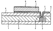
- FIG. 1 is a schematic view showing an organic EL display provided with a reflective electrode of the present invention.
- the inventors of the present invention have, in order from the substrate side, in the organic EL element including the laminated structure of the reflective electrode and the organic layer, particularly the reflective electrode in order from the substrate side.
- a first thin film made of pure Al or Al alloy hereinafter sometimes referred to as "Al-based film”
- Al-based film A first thin film made of pure Al or Al alloy
- nitrogen-containing Al or nitrogen-containing Al alloy directly connected to the organic layer
- the Al system laminated film of the above-mentioned composition By setting it as the Al system laminated film of the above-mentioned composition, high reflectance is securable by the 1st thin film which constitutes the Al system laminated film. Specifically, light emitted from the organic layer (organic light emitting layer) can be efficiently reflected. Further, an oxide conductive film directly connected to an organic layer of a reflective electrode (laminated structure of an oxide conductive film and an Ag alloy film) in which the work function of the second thin film constituting the Al-based laminated film is widely used. Since it is as high as the above, holes can be efficiently injected into the organic layer (organic light emitting layer) (excellent hole injection characteristics are exhibited).
- the oxide conductive film used in a general-purpose reflecting electrode can be omitted. That is, unlike general-purpose reflecting electrodes, it is not necessary to stack different materials such as an Ag alloy film and an oxide conductive film, and it is possible to use materials of the same composition and change only the type of film forming gas. is there. Therefore, the formation of the first thin film and the second thin film can be performed continuously in the sputtering process. As a result, in the present invention, the reflective electrode can be formed with high productivity, and consequently, the organic EL display and the organic EL illumination excellent in the light emission luminance characteristic can be manufactured with high productivity.
- the amount of nitrogen contained in the second thin film specifically, The ratio of nitrogen atoms to the total of nitrogen atoms and metal atoms constituting the thin film of 2, that is, N / [N + (Al or Al alloy)] is preferably 30 atomic% or more.
- the nitrogen content is more preferably 35 atomic% or more.
- the upper limit of the amount of nitrogen is about 50 atomic%.
- the component composition of the first thin film and the metal component composition of the second thin film may be pure Al or an Al alloy, and the composition conventionally used It can be adopted.
- at least one of the component composition of the first thin film and the metal component composition of the second thin film accounts for 0.05 to 5 atomic% of the rare earth element (in the second thin film, the proportion of the metal element excluding nitrogen
- the balance being Al and unavoidable impurities.
- Fe, Si, etc. are mentioned as an unavoidable impurity, It is permissible that 0.1 atomic% or less is contained, respectively.
- the rare earth element is an element that contributes to the improvement of the heat resistance of the first thin film and the second thin film.
- 0.05 atomic percent or more (more preferably 0.1 atomic percent or more, still more preferably 0.2 atomic percent or more, when the rare earth element is composed of a plurality of elements, the total amount is included) Is preferred.
- the content of the rare earth element is preferably 5 atomic percent or less (more preferably 3.0 atomic percent or less, still more preferably 1.0 atomic percent or less).
- the above-mentioned rare earth element means an element group obtained by adding Sc (scandium) and Y (yttrium) to a lanthanoid element (a total of 15 elements from La of atomic number 57 to Lu of atomic number 71 in the periodic table) .
- the preferred rare earth element used in the present invention is at least one selected from the group consisting of Nd, Gd, La, Y, Ce, Pr and Dy (more preferred rare earth elements are Nd and La). These elements may be added alone or in combination of two or more.
- At least one of the first thin film and the second thin film further contains Ni that contributes to the improvement of heat resistance, and Ge or Cu that contributes to the improvement of alkali corrosion resistance as alloy elements. It may be
- the heat resistance can be improved by setting the amount of Ni to preferably 0.1 atomic% or more (more preferably 0.3 atomic% or more).
- the amount of Ni is excessive, the reflectance of the first thin film is likely to decrease, so it is preferable to set the content to 2.0 atomic% or less (more preferably 1.5 atomic% or less).
- the alkali resistance is excellent by setting the content of at least one of Ge and Cu to preferably 0.1 atomic% or more (more preferably 0.3 atomic% or more). Corrosivity can be secured.
- the content of at least one of Ge and Cu is excessive, the reflectance is likely to be reduced, so that the total content is 2.0 atomic% or less (more preferably 1.5 atomic% or less). preferable.
- composition of the first thin film and the metal component composition of the second thin film are the same or different. The same is preferable from the viewpoint of simplification of the manufacturing process. Further, from the viewpoint of the characteristics of the Al-based laminated film, the type and amount of the additive element (alloy element) of the composition of the first thin film and the composition of the metal component of the second thin film may be different.
- the first thin film plays a role as a reflective film in the reflective electrode.
- the film thickness of the first thin film is preferably 50 nm or more, more preferably 100 nm or more, and the film thickness is preferably 600 nm or less, more preferably 500 nm It is below.
- the film thickness of the second thin film is preferably 0.5 nm or more and 10 nm or less.
- the film thickness of the second thin film is preferably 0.5 nm or more and 10 nm or less.
- the film thickness of the second thin film is preferably 1 nm or more.
- the reflectance of the reflective electrode is reduced, so the thickness is preferably 10 nm or less. More preferably, it is 5 nm or less, still more preferably 3 nm or less, still more preferably 2 nm or less.
- Method of forming a first thin film examples include a sputtering method and a vacuum evaporation method.
- a method of forming the first thin film (Al-based film) constituting the reflective electrode examples include a sputtering method and a vacuum evaporation method.
- the preferable conditions (film-forming conditions) of the said sputtering method are as follows. Substrate temperature: 25 ° C. or more, 200 ° C. or less (more preferably 150 ° C. or less) Deposition gas: inert gas (for example, Ar gas) -Gas pressure during film formation: 0.5 to 10 mTorr If the gas pressure is too low, the discharge becomes unstable, so the gas pressure is preferably 0.5 mTorr or more as described above. Further, if the gas pressure is too high, the surface of the formed film is likely to be roughened, so the gas pressure is preferably 10 mTorr or less as described above.
- the reflective electrode is formed by the sputtering method, that is, the first thin film is formed by the sputtering method, or the second thin film is formed by the method (A) described later, or both of them are formed by the sputtering method.
- the sputtering target used preferably contains 0.05 to 5 atomic% of a rare earth element (more preferably, one or more elements selected from the group consisting of Nd, Gd, La, Y, Ce, Pr and Dy). It is preferable to use an Al alloy sputtering target having the same composition as the desired Al alloy composition, the balance being Al and unavoidable impurities. If the Al alloy sputtering target is used, the first thin film or the second thin film having a desired component composition may be formed without the risk of composition deviation.
- the shape of the Al alloy sputtering target includes one processed into an arbitrary shape (a square plate, a circular plate, a donut plate, etc.) according to the shape and structure of the sputtering apparatus.
- a method of producing the Al alloy sputtering target a method of producing an ingot composed of an Al-based alloy by a melt casting method, a powder sintering method, a spray forming method, a preform composed of an Al-based alloy (final After manufacturing the intermediate body before obtaining a compact body, the method obtained by densifying this preform by a densification means is mentioned.
- a second thin film (nitrogen-containing Al-based film) constituting the reflective electrode is formed directly on the first thin film.
- the following method (A) or (B) is preferably used.
- a first thin film is formed by sputtering in an inert gas as described above, and then a second thin film is formed by sputtering (preferably under the following conditions).
- the formation of the second thin film is performed using the same Al alloy sputtering target as the Al alloy sputtering target used for forming the first thin film, and the metal component composition is the composition of the first thin film And the same film.
- Substrate temperature 25 ° C. or more, 150 ° C. or less (more preferably 100 ° C. or less)
- Film forming gas mixed gas of inert gas (for example, Ar gas) and nitrogen gas
- Nitrogen gas flow ratio 20 to 30% -Gas pressure during film formation: 0.5 to 10 mTorr If the gas pressure is too low, the discharge becomes unstable, so the gas pressure is preferably 0.5 mTorr or more as described above. Further, if the gas pressure is too high, the surface of the formed film is likely to be roughened, so the gas pressure is preferably 10 mTorr or less as described above.
- reverse sputtering applying a voltage to the substrate side using an RF power source without applying a voltage to the target side and causing ions to collide with the substrate side is called “reverse sputtering”.
- the following conditions are conditions in which a 4-inch substrate is placed opposite to a 4-inch target and nitrogen plasma treatment is performed by reverse sputtering.
- Power 100 W or more and 300 W or less If the power is too low, the nitrogen plasma treatment is not sufficiently performed and the second thin film is difficult to be formed, so 100 W or more is preferable. On the other hand, even if the power is too high, surface roughness occurs and the reflectance decreases, so the power is preferably 300 W or less. More preferably, it is 250 W or less.
- Treatment time 1 minute or more and 10 minutes or less If the treatment time is too short, the nitrogen plasma treatment is not sufficiently performed and the second thin film is difficult to be formed, so 1 minute or more is preferable. More preferably, it is 2 minutes or more. On the other hand, if the treatment time is too long, the process cost becomes high, so 10 minutes or less is preferable. More preferably, it is 8 minutes or less, More preferably, it is 5 minutes or less.
- Substrate temperature 25 ° C. or more, 150 ° C. or less (more preferably 100 ° C. or less)
- Gas used for treatment nitrogen gas
- Gas pressure during treatment 0.5 to 10 mTorr If the gas pressure is too low, the discharge becomes unstable, so the gas pressure is preferably 0.5 mTorr or more as described above. Further, if the gas pressure is too high, the thin film surface is likely to be roughened, so the gas pressure is preferably 10 mTorr or less as described above.
- the reflective electrode which is the characterizing portion of the present invention has been described. Below, the structure of the organic EL element containing this reflecting electrode is demonstrated.
- FIG. 1 shows an example of the organic EL display.
- the present invention is characterized in that the reflective electrode is composed of the first thin film and the second thin film, and the film directly connected to the organic layer is the second thin film (Al alloy film containing nitrogen).
- the other configuration is not limited to that shown in FIG. 1, and any known configuration commonly used in the field of organic EL displays can be adopted.
- the reflective electrode according to the present invention is not limited to the above-mentioned reflective anode electrode, and may be used for other reflective electrodes.
- the TFT 2 and the passivation film 3 are formed on the substrate 1, and the planarization layer 4 is further formed thereon.
- a contact hole 5 is formed on the TFT 2, and a source / drain electrode (not shown) of the TFT 2 via the contact hole 5 and a first thin film (Al-based film) 6 constituting a reflection electrode according to the present invention Are electrically connected.
- a second thin film (a nitrogen-containing Al-based film) 7 is formed directly on the first thin film 6.
- the formation of the first thin film 6 and the second thin film 7 can be performed by the method described above.
- the organic layer 8 is formed on the second thin film 7.
- the organic layer 8 may include, for example, a hole transport layer, an electron transport layer, and the like in addition to the organic light emitting layer.
- the cathode electrode 9 is formed on the organic layer 8. In the case of FIG. 1, any conventionally used material can be used for the material of the cathode electrode 9 regardless of the material used.
- the organic EL display In the organic EL display, light emitted from the organic light emitting layer in the organic layer 8 is efficiently reflected by the reflective anode electrode (in particular, the first thin film 6) of the present invention, so that excellent luminance can be realized. .
- a reflectance of 85% or more, preferably 87% or more is required.
- the reflective anode electrode have higher hole injection characteristics to the organic layer, and the work function of the surface is preferably 4.9 to 5.0 eV or more.
- Example 1 samples simulating the reflective electrode were formed under various conditions, and the work function and the reflectance were evaluated.
- a SiN film (film thickness: 300 nm) which is a passivation film was formed on the surface by a plasma CVD apparatus.
- an Al-based film (film thickness: about 100 nm) having the composition of Table 1 was formed as a first thin film by sputtering on the surface.
- the second thin film (the nitrogen-containing Al-based film) was continuously formed by sputtering according to the method (A).
- the film forming conditions for the first thin film and the second thin film are: substrate temperature: 25 ° C., gas pressure (pressure) during film formation: 2 mTorr, (DC) power: It was 200W.
- Ar was used for the first thin film
- Ar and nitrogen gas (the nitrogen gas flow ratio was 5% to 30%) were used for the second thin film.
- an Al alloy sputtering target (sputtering target having a size of 4 inches in diameter) having the same composition as each Al alloy composition shown in Table 1 was used.
- the same sputtering target as used for the first thin film formation was used to form the second thin film.
- an Al-0.2 atomic% Nd film, an Al-0.6 atomic% Ni-0.5 atomic% Cu-0.3 atomic% La film, or an Al-0.6 atomic% Nd film ( In all cases, a film thickness of about 100 nm was formed by sputtering in the same manner as described above, and a sample in which the second thin film was not formed was also prepared.
- the composition of the first thin film was identified by ICP emission analysis.
- the nitrogen content of the second thin film was identified by XPS analysis using a device whose device name is “HiRUPE” (High-energy Reflection EELS / UPS / Plasmon loss / ESCA).
- the XPS analysis was performed on a sample formed at a nitrogen gas flow rate ratio of 10% and a sample formed at a nitrogen gas flow rate ratio of 20%.
- the nitrogen content of the second thin film was 25 atomic% and 40 atomic%, respectively.
- the nitrogen content of the second thin film was obtained when the nitrogen gas flow ratio was other than 10% and 20%.
- the second thin film may contain oxygen in addition to the Al alloy and nitrogen, in the present invention, the nitrogen atoms occupying the total of nitrogen atoms and metal atoms constituting the second thin film are not taken into consideration.
- the ratio was taken as the amount of nitrogen of the second thin film.
- the nitrogen content of the second thin film is made to be a certain amount or more regardless of the alloy composition of the first thin film or the second thin film. I understand that is good. Furthermore, no. From the results of 5 and 20, it can be seen that the thickness of the second thin film should be 10 nm or less in order to obtain high reflectance.
- Example 2 In the present example, the first thin film was formed in the same manner as in Example 1. Next, nitrogen plasma treatment was performed on the surface of the first thin film (the surface exposed to the outside air) under the following conditions to form a second thin film. The nitrogen plasma treatment was continuously performed in the same sputtering apparatus immediately after the first thin film was formed using the reverse sputtering function of the sputtering apparatus. Processing conditions were as follows: substrate temperature: 25 ° C., gas: N 2 gas, pressure: 2 mTorr, power and processing time shown in Table 2.
- the numbers in Table 2 are as follows.
- the film thickness of the second thin film of No. 4 was calculated using a Riken Keiki AC-2 and a calibration curve was calculated. As a result, it was 0.8 nm at the thinnest portion.
- the thickness of the second thin film of the other samples was also in the range of 0.5 nm to 10 nm. Further, in any of the examples, the nitrogen content of the second thin film was in the range of 30 to 50 atomic%.
- No. No. 1 is only the Al alloy film corresponding to the first thin film of the present invention, and the work function becomes small because the second thin film (nitrogen-containing Al alloy film) is not included.
- a reflective electrode composed of an Al-based laminated film of a first thin film made of pure Al or Al alloy and a second thin film made of nitrogen-containing Al or nitrogen-containing Al alloy has high reflectance. And a high hole injection characteristic, it can be applied to a reflective electrode of an organic EL element in place of a reflective electrode including an oxide conductive film conventionally used.
- a reflective electrode according to the present invention materials of the same composition are used instead of laminating different materials like the conventional reflective electrode (laminated film of an oxide conductive film and a metal film). Since it can be formed, an organic EL display, an organic EL illumination, and the like excellent in light emission luminance characteristics can be manufactured with high productivity.
Landscapes
- Chemical & Material Sciences (AREA)
- Chemical Kinetics & Catalysis (AREA)
- Engineering & Computer Science (AREA)
- Materials Engineering (AREA)
- Mechanical Engineering (AREA)
- Metallurgy (AREA)
- Organic Chemistry (AREA)
- Electroluminescent Light Sources (AREA)
Description
本発明は、有機EL素子、有機EL素子の反射電極の製造方法、および有機EL素子の反射電極形成用Al合金スパッタリングターゲットに関するものであり、例えば、有機ELディスプレイや有機EL照明において使用される有機EL素子と、この有機EL素子を構成する反射電極の製造方法、更には、有機EL素子の反射電極形成用Al合金スパッタリングターゲットに関するものである。
尚、以下では、有機ELディスプレイを例に説明するが、本発明はこれに限定されない。
自発光型のフラットパネルディスプレイの1つである有機エレクトロルミネッセンス(以下、「有機EL」と記載する)ディスプレイは、ガラス板などの基板上に有機EL素子をマトリックス状に配列して形成した全固体型のフラットパネルディスプレイである。有機ELディスプレイでは、陽極(アノード)と陰極(カソード)とがストライプ状に形成されており、それらが交差する部分が画素(有機EL素子)にあたる。この有機EL素子に外部から数Vの電圧を印加して電流を流すことで、有機分子が励起状態に押し上げられ、この励起状態の有機分子が元の基底状態(安定状態)へ戻るときに生じるエネルギーが光として放出される。この発光色は有機材料に固有のものである。
有機EL素子は、自発光型かつ電流駆動型の素子であり、その駆動方式にはパッシブ型とアクティブ型がある。パッシブ型は構造が簡単であるが、フルカラー化が困難である。一方アクティブ型は大型化が可能であり、フルカラー化にも適しているが、TFT基板が必要である。このTFT基板には低温多結晶Si(p-Si)またはアモルファスSi(a-Si)などのTFTが使われている。
このアクティブ型の有機ELディスプレイの場合、複数のTFTや配線が障害となって、有機EL画素に使用できる面積が小さくなる。駆動回路が複雑となりTFTの数が増えてくると、さらにその影響は大きくなる。そこで最近では、ガラス基板から光を取り出すのではなく、上面側から光を取り出す構造(トップエミッション)にすることで、開口率を改善する方法が注目されている。
このようなアクティブ型のトップエミッション有機ELディスプレイでは、有機層の下面(TFT基板側)の陽極(アノード電極)に、正孔注入特性に優れるITO(酸化インジウムスズ)やIZO(酸化インジウム亜鉛)に代表される透明酸化物導電膜が用いられる。また、発光層から放射された光を反射する目的を兼ねて、上記アノード電極は、上記透明酸化物導電膜と反射膜との積層構造とされる。該反射膜としては、モリブデン(Mo)、クロム(Cr)、アルミニウム(Al)や銀(Ag)などの反射性金属膜が用いられることが多い。例えば、既に量産されているトップエミッション方式の有機ELディスプレイにおける反射アノード電極には、ITOとAg合金膜との積層構造が採用されている。
反射率を考慮すれば、AgまたはAgを主体として含むAg合金膜が、反射率が高いため有用である。Ag合金膜は、耐食性に劣るという特有の課題を抱えているが、その上に積層されるITO膜で当該Ag合金膜を被覆することにより、上記課題を解消することができる。しかしながら、Agは材料コストが高いことに加え、成膜に必要なスパッタリングターゲットの大型化が難しいという問題がある。よって、例えば大型テレビなどのような、大型のアクティブマトリックス型のトップエミッション有機ELディスプレイの上記反射膜に、Ag合金膜を適用するのは困難である。
一方、反射率のみを考慮すれば、Alも反射膜として良好である。例えば特許文献1には、反射電極(反射膜)を構成する金属膜として、Niを0.1~2原子%含有するAl-Ni合金膜が提案されており、このAl-Ni合金膜は、純Al並みの高い反射率を有し、且つ、上記Al-Ni合金膜をITO膜やIZO膜などの酸化物導電膜と直接接続させても低い接触抵抗を実現できることが示されている。
上記特許文献1の技術では、上述の通り、反射電極の構成に上記ITO等の酸化物導電膜が必要である。これに対し特許文献2では、反射アノード電極と一般的な積層構造の有機層の間に、更に別の有機層を追加挿入することにより、反射アノード電極に酸化物導電膜を用いないAl合金単層の場合であっても、十分な正孔注入特性を実現できることが提案されている。
しかしながら、上記特許文献2の技術では、有機層の蒸着工程が1段階増えることになる。よって生産性の点から、上記余分な有機層を追加させることなく従来の有機層の構成で、酸化物導電膜を必要とせずとも十分な正孔注入特性を示し、かつ反射電極として必要な高い反射率を実現できる、Al系反射電極が求められている。
本発明は上記の様な事情に着目してなされたものであって、その目的は、従来の有機層の構成を採用でき、かつ、従来の反射電極(特には反射アノード電極)で使用されていた酸化物導電膜を用いずに、高い正孔注入特性と高反射率を示す反射電極を含む、有機EL素子を実現することにある。
本発明は、以下の有機EL素子、有機EL素子の反射電極の製造方法、有機EL素子の反射電極形成用Al合金スパッタリングターゲット、有機ELディスプレイおよび有機EL照明を提供する。
(1)基板と、反射電極と有機層の積層構造をこの順で含む有機EL素子であって、
前記反射電極は、前記基板側から順に、純AlまたはAl合金からなる第1の薄膜と、窒素含有Alまたは窒素含有Al合金からなる第2の薄膜とのAl系積層膜で構成され、かつ、前記第2の薄膜は前記有機層と直接接続していることを特徴とする有機EL素子。
(1)基板と、反射電極と有機層の積層構造をこの順で含む有機EL素子であって、
前記反射電極は、前記基板側から順に、純AlまたはAl合金からなる第1の薄膜と、窒素含有Alまたは窒素含有Al合金からなる第2の薄膜とのAl系積層膜で構成され、かつ、前記第2の薄膜は前記有機層と直接接続していることを特徴とする有機EL素子。
(2)前記第2の薄膜に含まれる窒素量は、30原子%以上50原子%以下である(1)に記載の有機EL素子。
(3)前記第2の薄膜の厚さは0.5nm以上10nm以下である(1)または(2)に記載の有機EL素子。
(3)前記第2の薄膜の厚さは0.5nm以上10nm以下である(1)または(2)に記載の有機EL素子。
(4)前記第1の薄膜および前記第2の薄膜の少なくとも一方は、合金元素として、希土類元素を0.05~5原子%含有するものである(1)~(3)のいずれか一つに記載の有機EL素子。
(5)前記希土類元素は、Nd,Gd,La,Y,Ce,PrおよびDyよりなる群から選択される1種類以上の元素である(4)に記載の有機EL素子。
(5)前記希土類元素は、Nd,Gd,La,Y,Ce,PrおよびDyよりなる群から選択される1種類以上の元素である(4)に記載の有機EL素子。
(6)(1)~(5)のいずれか一つに記載の有機EL素子の反射電極を製造する方法であって、
前記第1の薄膜を、不活性ガス中にてスパッタリング法で形成する工程、および、前記第2の薄膜を、不活性ガスと窒素ガスの混合ガス中にてスパッタリング法で形成する工程を含む有機EL素子の反射電極の製造方法。
前記第1の薄膜を、不活性ガス中にてスパッタリング法で形成する工程、および、前記第2の薄膜を、不活性ガスと窒素ガスの混合ガス中にてスパッタリング法で形成する工程を含む有機EL素子の反射電極の製造方法。
(7)(1)~(5)のいずれか一つに記載の有機EL素子の反射電極を製造する方法であって、
前記第1の薄膜を、不活性ガス中にてスパッタリング法で形成する工程、および、前記第2の薄膜を、前記第1の薄膜の表面に窒素プラズマ処理を行って形成する工程を含む有機EL素子の反射電極の製造方法。
前記第1の薄膜を、不活性ガス中にてスパッタリング法で形成する工程、および、前記第2の薄膜を、前記第1の薄膜の表面に窒素プラズマ処理を行って形成する工程を含む有機EL素子の反射電極の製造方法。
(8)(1)~(5)のいずれか一つに記載の有機EL素子の反射電極形成用Al合金スパッタリングターゲットであって、希土類元素を0.05~5原子%含有することを特徴とする有機EL素子の反射電極形成用Al合金スパッタリングターゲット。
(9)前記希土類元素は、Nd,Gd,La,Y,Ce,PrおよびDyよりなる群から選択される1種類以上の元素である(8)に記載のAl合金スパッタリングターゲット。
(9)前記希土類元素は、Nd,Gd,La,Y,Ce,PrおよびDyよりなる群から選択される1種類以上の元素である(8)に記載のAl合金スパッタリングターゲット。
(10)(1)~(5)のいずれか一つに記載の有機EL素子を備えた有機ELディスプレイ。
(11)(1)~(5)のいずれか一つに記載の有機EL素子を備えた有機EL照明。
(11)(1)~(5)のいずれか一つに記載の有機EL素子を備えた有機EL照明。
本発明によれば、純AlまたはAl合金からなる第1の薄膜と、窒素含有Alまたは窒素含有Al合金からなる第2の薄膜とのAl系積層膜で構成される反射電極が、高い反射率を示すと共に高い正孔注入特性を示すため、従来用いられてきた酸化物導電膜を含む反射電極に代えて、有機EL素子の反射電極に適用することができる。
その結果、本発明に係る反射電極の製造方法において、従来の反射電極(酸化物導電膜と金属膜の積層膜)のように異質の材料を積層させるのではなく、同一組成の材料を用いて形成できることから、発光輝度特性に優れた有機ELディスプレイや有機EL照明等を、生産性良く製造することができる。
以下、単に「純AlまたはAl合金(膜)」というときは、「窒素を含有しない純AlまたはAl合金(膜)」をいう。
本発明者らは、前記課題を解決するために鋭意研究を重ねた結果、基板側から順に、反射電極と有機層の積層構造を含む有機EL素子において、特に反射電極を、前記基板側から順に、純AlまたはAl合金からなる第1の薄膜(以下「Al系膜」ということがある)と、窒素含有Alまたは窒素含有Al合金からなる第2の薄膜(前記有機層と直接接続している。以下「窒素含有Al系膜」ということがある)とのAl系積層膜とすればよいことを見出した。
上記構成のAl系積層膜とすることによって、該Al系積層膜を構成する第1の薄膜で高い反射率を確保できる。具体的には、有機層(有機発光層)から放射された光を効率よく反射できる。また、前記Al系積層膜を構成する第2の薄膜の仕事関数が、汎用されている反射電極(酸化物導電膜とAg合金膜の積層構造)の、有機層と直接接続する酸化物導電膜と同程度に高いため、有機層(有機発光層)に効率よく正孔を注入できる(優れた正孔注入特性を発揮する)。
本発明によれば、汎用の反射電極で用いられている酸化物導電膜を省略できる。即ち、汎用の反射電極のように、Ag合金膜と酸化物導電膜といった異なる材料を積層させる必要がなく、同一組成の材料を用い成膜ガスの種類のみを変更して形成することが可能である。よって、前記第1の薄膜と前記第2の薄膜の形成はスパッタリング工程で連続して行うことが可能である。その結果、本発明では反射電極を生産性良く形成することができ、ひいては、発光輝度特性に優れた有機ELディスプレイや有機EL照明を生産性良く製造することができる。
前記第2の薄膜の正孔注入特性を十分に高める、即ち、前記第2の薄膜の仕事関数を十分に高めるには、該第2の薄膜中に含まれる窒素量、具体的には、第2の薄膜を構成する窒素原子と金属原子の合計に占める窒素原子の割合、即ち、N/[N+(AlまたはAl合金)]を、30原子%以上とすることが好ましい。前記窒素量はより好ましくは35原子%以上である。一方、窒化Alや窒化Al合金の場合、AlとNの組成比は1:1であるので、前記窒素量の上限は約50原子%となる。
(第1の薄膜の成分組成と第2の薄膜の金属成分組成)
本発明において、第1の薄膜の成分組成と第2の薄膜の金属成分組成(窒素を除いた組成をいう。以下同じ)は、純AlまたはAl合金であればよく、従来より用いられる組成を採用することができる。第1の薄膜の成分組成および第2の薄膜の金属成分組成の少なくとも一方は、好ましくは、希土類元素を0.05~5原子%(第2の薄膜においては、窒素を除く金属元素に占める割合をいう。以下同じ)含有し、残部がAlおよび不可避的不純物である。不可避不純物としては、Fe、Si等が挙げられ、それぞれ0.1原子%以下含まれることが許容される。
本発明において、第1の薄膜の成分組成と第2の薄膜の金属成分組成(窒素を除いた組成をいう。以下同じ)は、純AlまたはAl合金であればよく、従来より用いられる組成を採用することができる。第1の薄膜の成分組成および第2の薄膜の金属成分組成の少なくとも一方は、好ましくは、希土類元素を0.05~5原子%(第2の薄膜においては、窒素を除く金属元素に占める割合をいう。以下同じ)含有し、残部がAlおよび不可避的不純物である。不可避不純物としては、Fe、Si等が挙げられ、それぞれ0.1原子%以下含まれることが許容される。
希土類元素は、第1の薄膜や第2の薄膜の耐熱性向上に寄与する元素である。本発明では、上記の通り0.05原子%以上(より好ましくは0.1原子%以上、更に好ましくは0.2原子%以上、希土類元素が複数の元素からなる場合は合計量をいう)含むことが好ましい。耐熱性向上の観点からは、希土類元素の含有量が高いほどよいが、その量が多すぎると、特に第1の薄膜(Al系膜)の反射率が低下しやすくなる。よって希土類元素の含有量は、5原子%以下(より好ましくは3.0原子%以下、更に好ましくは1.0原子%以下)であることが好ましい。
上記希土類元素とは、ランタノイド元素(周期表において、原子番号57のLaから原子番号71のLuまでの合計15元素)に、Sc(スカンジウム)とY(イットリウム)とを加えた元素群を意味する。本発明に用いられる好ましい希土類元素は、Nd,Gd,La,Y,Ce,PrおよびDyよりなる群から選択される少なくとも1種(より好ましい希土類元素は、Nd、La)である。これらの元素は、単独で添加しても良いし、二種以上を併用しても良い。
また第1の薄膜および第2の薄膜の少なくとも一方は、上記希土類元素に加えて更に、耐熱性向上に寄与するNiや、耐アルカリ腐食性向上に寄与するGeやCuを、合金元素として含んでいてもよい。
上記Niを含有させる場合は、Ni量を好ましくは0.1原子%以上(より好ましくは0.3原子%以上)とすることで耐熱性を向上させることができる。一方、Ni量が過剰になると、第1の薄膜の反射率が低下しやすくなるため、2.0原子%以下(より好ましくは1.5原子%以下)とすることが好ましい。
上記GeやCuを含有させる場合は、GeおよびCuの少なくとも一方の含有量を合計で、好ましくは0.1原子%以上(より好ましくは0.3原子%以上)とすることで優れた耐アルカリ腐食性を確保することができる。一方、GeおよびCuの少なくとも一方の含有量が過剰になると、反射率がかえって低下しやすくなるため、合計で、2.0原子%以下(より好ましくは1.5原子%以下)とすることが好ましい。
前記第1の薄膜の組成と、前記第2の薄膜の金属成分組成は、同一または異なる。作製プロセス簡略化の観点からは同一であることが好ましい。また、Al系積層膜の特性の観点からは、第1の薄膜の組成と第2の薄膜の金属成分組成の、添加元素(合金元素)の種類や量が異なっていてもよい。
(第1の薄膜の膜厚)
第1の薄膜(Al系膜)は、反射電極における反射膜としての役割を担う。高い反射率を確保するため、第1の薄膜の膜厚は、50nm以上とすることが好ましく、より好ましくは100nm以上であり、前記膜厚は、600nm以下とすることが好ましく、より好ましくは500nm以下である。
第1の薄膜(Al系膜)は、反射電極における反射膜としての役割を担う。高い反射率を確保するため、第1の薄膜の膜厚は、50nm以上とすることが好ましく、より好ましくは100nm以上であり、前記膜厚は、600nm以下とすることが好ましく、より好ましくは500nm以下である。
(第2の薄膜の膜厚)
第2の薄膜(窒素含有Al系膜)の膜厚は、0.5nm以上10nm以下であることが好ましい。第2の薄膜の膜厚を0.5nm以上とすることによって、優れた正孔注入特性を確実に達成できる。より好ましくは1nm以上である。一方、第2の薄膜の膜厚が厚すぎると、反射電極の反射率が低下するため、10nm以下であることが好ましい。より好ましくは5nm以下、更に好ましくは3nm以下、より更に好ましくは2nm以下である。
第2の薄膜(窒素含有Al系膜)の膜厚は、0.5nm以上10nm以下であることが好ましい。第2の薄膜の膜厚を0.5nm以上とすることによって、優れた正孔注入特性を確実に達成できる。より好ましくは1nm以上である。一方、第2の薄膜の膜厚が厚すぎると、反射電極の反射率が低下するため、10nm以下であることが好ましい。より好ましくは5nm以下、更に好ましくは3nm以下、より更に好ましくは2nm以下である。
(第1の薄膜の形成方法)
反射電極を構成する第1の薄膜(Al系膜)の形成方法として、例えば、スパッタリング法や真空蒸着法などが挙げられる。本発明では、細線化や膜内の合金成分の均一化を図ることができ、かつ添加元素量を容易にコントロールできる等の観点から、第1の薄膜をスパッタリング法で形成することが好ましい。
反射電極を構成する第1の薄膜(Al系膜)の形成方法として、例えば、スパッタリング法や真空蒸着法などが挙げられる。本発明では、細線化や膜内の合金成分の均一化を図ることができ、かつ添加元素量を容易にコントロールできる等の観点から、第1の薄膜をスパッタリング法で形成することが好ましい。
前記スパッタリング法の好ましい条件(成膜条件)は以下の通りである。
・基板温度:25℃以上、200℃以下(より好ましくは150℃以下)
・成膜ガス:不活性ガス(例えば、Arガス)
・成膜時のガス圧:0.5~10mTorr
上記ガス圧が低すぎると放電が不安定になるため、ガス圧は、上記の通り0.5mTorr以上とすることが好ましい。また、上記ガス圧が高すぎると、形成される膜に表面荒れが生じ易くなるため、ガス圧は、上記の通り10mTorr以下とすることが好ましい。
・基板温度:25℃以上、200℃以下(より好ましくは150℃以下)
・成膜ガス:不活性ガス(例えば、Arガス)
・成膜時のガス圧:0.5~10mTorr
上記ガス圧が低すぎると放電が不安定になるため、ガス圧は、上記の通り0.5mTorr以上とすることが好ましい。また、上記ガス圧が高すぎると、形成される膜に表面荒れが生じ易くなるため、ガス圧は、上記の通り10mTorr以下とすることが好ましい。
上記スパッタリング法で反射電極を形成、即ち、上記スパッタリング法で第1の薄膜を形成、または、後述する(A)の方法で第2の薄膜を形成、または両方を行うには、該スパッタリング法で用いるスパッタリングターゲットとして、好ましくは希土類元素(より好ましくはNd,Gd,La,Y,Ce,PrおよびDyよりなる群から選択される1種類以上の元素)を0.05~5原子%含むものであって、残部がAlおよび不可避不純物である、所望のAl合金組成と同一組成のAl合金スパッタリングターゲットを用いるのがよい。該Al合金スパッタリングターゲットを用いれば、組成ズレの恐れがなく、所望の成分組成の第1の薄膜や第2の薄膜を形成できるのでよい。
上記Al合金スパッタリングターゲットの形状は、スパッタリング装置の形状や構造に応じて任意の形状(角型プレート状、円形プレート状、ドーナツプレート状など)に加工したものが含まれる。
上記Al合金スパッタリングターゲットの製造方法としては、溶解鋳造法や粉末焼結法、スプレイフォーミング法で、Al基合金からなるインゴットを製造して得る方法や、Al基合金からなるプリフォーム(最終的な緻密体を得る前の中間体)を製造した後、該プリフォームを緻密化手段により緻密化して得られる方法が挙げられる。
(第2の薄膜の形成方法)
反射電極を構成する第2の薄膜(窒素含有Al系膜)は、前記第1の薄膜の直上に形成される。この第2の薄膜の形成方法として、下記(A)または(B)の方法が好ましく用いられる。
反射電極を構成する第2の薄膜(窒素含有Al系膜)は、前記第1の薄膜の直上に形成される。この第2の薄膜の形成方法として、下記(A)または(B)の方法が好ましく用いられる。
(A)第1の薄膜を上述の通り不活性ガス中にてスパッタリング法で形成後、続けて第2の薄膜をスパッタリング法(好ましくは下記の条件)で形成する。
好ましい実施形態として、前記第2の薄膜の形成を、第1の薄膜の形成に用いたAl合金スパッタリングターゲットと同一のAl合金スパッタリングターゲットを用いて行い、金属成分組成が、第1の薄膜の組成と同一の膜を形成することが挙げられる。
・基板温度:25℃以上、150℃以下(より好ましくは100℃以下)
・成膜ガス:不活性ガス(例えば、Arガス)と窒素ガスの混合ガス
・窒素ガス流量比率:20~30%
・成膜時のガス圧:0.5~10mTorr
上記ガス圧が低すぎると放電が不安定になるため、ガス圧は、上記の通り0.5mTorr以上とすることが好ましい。また、上記ガス圧が高すぎると、形成される膜に表面荒れが生じ易くなるため、ガス圧は、上記の通り10mTorr以下とすることが好ましい。
・成膜ガス:不活性ガス(例えば、Arガス)と窒素ガスの混合ガス
・窒素ガス流量比率:20~30%
・成膜時のガス圧:0.5~10mTorr
上記ガス圧が低すぎると放電が不安定になるため、ガス圧は、上記の通り0.5mTorr以上とすることが好ましい。また、上記ガス圧が高すぎると、形成される膜に表面荒れが生じ易くなるため、ガス圧は、上記の通り10mTorr以下とすることが好ましい。
(B)第1の薄膜を上述の通り不活性ガス中にてスパッタリング法で形成後、該第1の薄膜の表面に窒素プラズマ処理(好ましくは下記の条件)を行って第2の薄膜を形成する。
スパッタリング装置で、ターゲット側に電圧を印加せずに、基板側にRF電源を用いて電圧を印加し、イオンを基板側に衝突させることを「逆スパッタリング」という。下記条件は、4インチターゲットと対向して4インチ基板を設置し、逆スパッタリングによって窒素プラズマ処理を行った場合の条件である。
・パワー:100W以上300W以下
上記パワーが低すぎると窒素プラズマ処理が十分に行われず、第2の薄膜が形成されにくいため、100W以上とするのがよい。一方、上記パワーが高すぎても表面荒れが生じて反射率が低下するため300W以下とするのがよい。より好ましくは250W以下である。
上記パワーが低すぎると窒素プラズマ処理が十分に行われず、第2の薄膜が形成されにくいため、100W以上とするのがよい。一方、上記パワーが高すぎても表面荒れが生じて反射率が低下するため300W以下とするのがよい。より好ましくは250W以下である。
・処理時間:1分以上10分以下
上記処理時間が短すぎると窒素プラズマ処理が十分に行われず、第2の薄膜が形成されにくいため、1分以上とするのがよい。より好ましくは2分以上である。一方、処理時間が長すぎるとプロセスコストが高くなるため、10分以下とするのがよい。より好ましくは8分以下、更に好ましくは5分以下である。
上記処理時間が短すぎると窒素プラズマ処理が十分に行われず、第2の薄膜が形成されにくいため、1分以上とするのがよい。より好ましくは2分以上である。一方、処理時間が長すぎるとプロセスコストが高くなるため、10分以下とするのがよい。より好ましくは8分以下、更に好ましくは5分以下である。
・基板温度:25℃以上、150℃以下(より好ましくは100℃以下)
・処理に用いるガス:窒素ガス
・処理時のガス圧:0.5~10mTorr
上記ガス圧が低すぎると放電が不安定になるため、ガス圧は、上記の通り0.5mTorr以上とすることが好ましい。また、上記ガス圧が高すぎると、薄膜表面の荒れが生じ易くなるため、ガス圧は、上記の通り10mTorr以下とすることが好ましい。
・処理に用いるガス:窒素ガス
・処理時のガス圧:0.5~10mTorr
上記ガス圧が低すぎると放電が不安定になるため、ガス圧は、上記の通り0.5mTorr以上とすることが好ましい。また、上記ガス圧が高すぎると、薄膜表面の荒れが生じ易くなるため、ガス圧は、上記の通り10mTorr以下とすることが好ましい。
以上、本発明の特徴部分である反射電極について説明した。以下では、この反射電極を含む有機EL素子の構造について説明する。
図1に示す有機ELディスプレイを例に用いて、本発明の反射電極を含む積層構造を説明する。下記では、本発明の有機EL素子を、有機ELディスプレイに適用する場合について説明するが、本発明の有機EL素子は、その適用が有機ELディスプレイに限定されるものではなく、有機EL照明等にも適用することができる。また図1は、有機ELディスプレイの一例を示すものである。本発明は、反射電極が前記第1の薄膜と第2の薄膜で構成され、かつ有機層と直接接続する膜が第2の薄膜(窒素を含有するAl合金膜)である点に特徴があり、それ以外の構成は図1に限定されず、有機ELディスプレイの分野で通常用いられる公知の構成を採用することができる。更に、本発明にかかる反射電極は、上記反射アノード電極に限定されず、その他の反射電極にも使用しうる。
まず図1に示す通り、基板1上にTFT2およびパシベーション膜3が形成され、さらにその上に平坦化層4が形成される。TFT2上にはコンタクトホール5が形成され、コンタクトホール5を介してTFT2のソース・ドレイン電極(図示せず)と、本発明に係る反射電極を構成する第1の薄膜(Al系膜)6とは電気的に接続されている。
更に第1の薄膜6の直上に第2の薄膜(窒素含有Al系膜)7が形成される。上記第1の薄膜6と第2の薄膜7の形成は、上述した方法で行うことができる。
次いで、第2の薄膜7の上に、有機層8が形成される。上記有機層8には、有機発光層の他に例えば正孔輸送層や電子輸送層などが含まれうる。さらに有機層8の上にカソード電極9が形成される。この図1の場合、カソード電極9を構成する材料については特に問わず、従来より用いられているものを使用することができる。
上記有機ELディスプレイでは、有機層8中の有機発光層から放射された光が本発明の反射アノード電極(特には第1の薄膜6)で効率よく反射されるので、優れた発光輝度を実現できる。なお反射電極(第1の薄膜6+第2の薄膜7)の反射率は高いほどよく、一般的には85%以上、好ましくは87%以上の反射率が求められる。
また、反射アノード電極は有機層への正孔注入特性が高いほどよく、表面の仕事関数が4.9~5.0eV以上であることが好ましい。
以下、実施例を挙げて本発明をより具体的に説明するが、本発明はもとより下記実施例によって制限を受けるものではなく、前・後記の趣旨に適合し得る範囲で適当に変更を加えて実施することも勿論可能であり、それらはいずれも本発明の技術的範囲に包含される。
[実施例1]
本実施例では、反射電極を模擬した試料を種々の条件で形成し、仕事関数と反射率の評価を行った。
本実施例では、反射電極を模擬した試料を種々の条件で形成し、仕事関数と反射率の評価を行った。
具体的にはまず、無アルカリ硝子板(板厚:0.7mm)を基板として、その表面にパシベーション膜であるSiN膜(膜厚:300nm)をプラズマCVD装置によって成膜した。その成膜条件は、基板温度:280℃、ガス比:SiH4/NH3/N2=125/6/185、圧力:137Pa、RFパワー:100Wである。
さらにその表面に、第1の薄膜として、表1の組成のAl系膜(膜厚:約100nm)をスパッタリング法で成膜した。その後、上記(A)の方法で、第2の薄膜(窒素含有Al系膜)を続けてスパッタリング法で成膜した。前記第1の薄膜と第2の薄膜の成膜条件は、成膜ガスの種類を除き、いずれも、基板温度:25℃、成膜時のガス圧(圧力):2mTorr、(DC)パワー:200Wとした。成膜ガスは、第1の薄膜ではArを用い、第2の薄膜では、Arと窒素ガス(窒素ガス流量比率は5%~30%)を用いた。第1の薄膜の形成には、表1に示す各Al合金組成と同組成のAl合金スパッタリングターゲット(サイズが直径4インチのスパッタリングターゲット)を用いた。また第2の薄膜の形成には、前記第1の薄膜形成と同じスパッタリングターゲットを用いた。得られた第1の薄膜の組成(=第2の薄膜の金属成分組成)と、第2の薄膜の窒素量は表1に示すとおりである。
また比較例として、Al-0.2原子%Nd膜、Al-0.6原子%Ni-0.5原子%Cu-0.3原子%La膜、またはAl-0.6原子%Nd膜(いずれも膜厚:約100nm)を上記と同様にスパッタリング法で成膜し、かつ第2の薄膜は形成しない試料も用意した。
第1の薄膜の組成(=第2の薄膜の金属成分組成)は、ICP発光分析で同定した。また第2の薄膜の窒素量は、装置名が「HiRUPE」(High-energy Reflection EELS/UPS/Plasmon loss/ESCA)である装置を用いて、XPS分析で同定した。XPS分析は、窒素ガス流量比率10%で成膜した試料と窒素ガス流量比率20%で成膜した試料について実施した。その結果、第2の薄膜(窒素含有Al系膜)の窒素量は、それぞれ25原子%、40原子%であった。また、前記窒素ガス流量比率と第2の薄膜の窒素量との関係から、窒素ガス流量比率が10%と20%以外の場合の、第2の薄膜の窒素量を求めた。尚、第2の薄膜にはAl合金と窒素以外に酸素を含みうるが、本発明ではこの酸素を考慮せずに、第2の薄膜を構成する窒素原子と金属原子の合計に占める窒素原子の割合を、第2の薄膜の窒素量とした。
上記のように作製した各試料(反射電極)について、(1)仕事関数、および(2)反射率を、以下の通り測定して評価した。その結果を表1に示す。
(1)仕事関数
第2の薄膜の表面(第2の薄膜の外気にさらされている面)の仕事関数は、理研計器製AC-2を用いて測定した。なお、仕事関数は、第2の薄膜の表面状態(大気中の有機物汚染など)に敏感であるため、上記AC-2で測定する直前にUVオゾン照射を行った。そして、下記の通り5.0eVを基準とし、5.0eV以上の場合を〇(仕事関数が高い。正孔注入特性に優れている)と評価した。
○:5.0eV以上
×:5.0eV未満
第2の薄膜の表面(第2の薄膜の外気にさらされている面)の仕事関数は、理研計器製AC-2を用いて測定した。なお、仕事関数は、第2の薄膜の表面状態(大気中の有機物汚染など)に敏感であるため、上記AC-2で測定する直前にUVオゾン照射を行った。そして、下記の通り5.0eVを基準とし、5.0eV以上の場合を〇(仕事関数が高い。正孔注入特性に優れている)と評価した。
○:5.0eV以上
×:5.0eV未満
(2)反射率
反射率は、日本分光株式会社製の可視・紫外分光光度計「V-570」を用い、測定波長:850~250nmの範囲における分光反射率を測定した。具体的には、基準ミラーの反射光強度に対して、試料の反射光強度を測定した値を「反射率」とした。そして本実施例では、λ=450nmにおける反射率を基準として以下のように評価し、○または△を合格と判定した。
○:87%以上
△:85%以上87%未満
×:85%未満
反射率は、日本分光株式会社製の可視・紫外分光光度計「V-570」を用い、測定波長:850~250nmの範囲における分光反射率を測定した。具体的には、基準ミラーの反射光強度に対して、試料の反射光強度を測定した値を「反射率」とした。そして本実施例では、λ=450nmにおける反射率を基準として以下のように評価し、○または△を合格と判定した。
○:87%以上
△:85%以上87%未満
×:85%未満

表1より次の様に考察することができる。No.1、9および17は、本発明の第1の薄膜に該当するAl合金膜のみで、第2の薄膜(窒素含有Al合金膜)を有していないため、仕事関数が小さくなった。
また、No.7、8、14~16および22の結果から、高い仕事関数を確保するには、第1の薄膜や第2の薄膜の合金組成によらず、第2の薄膜の窒素量を一定以上とするのがよいことがわかる。更に、No.5および20の結果から、高い反射率を得るには、第2の薄膜の膜厚を10nm以下とするのがよいことがわかる。
これらに対し、No.2~4、6、10~13、18、19および21は、規定の第1の薄膜と第2の薄膜が形成されており、かつ第2の薄膜の窒素量と第2の薄膜の膜厚も好ましい範囲を満たしているため、十分高い仕事関数と反射率が得られた。
[実施例2]
本実施例では、実施例1と同様にして第1の薄膜まで形成した。次いで、第1の薄膜の表面(外気にさらされている面)に対し、窒素プラズマ処理を次に示す条件で行って第2の薄膜を形成した。窒素プラズマ処理は、スパッタ装置の逆スパッタ機能を用いて、第1の薄膜を成膜した直後に同じスパッタ装置で連続して実施した。処理条件は、基板温度:25℃、ガス:N2ガス、圧力:2mTorr、表2に示すパワーと処理時間とした。
本実施例では、実施例1と同様にして第1の薄膜まで形成した。次いで、第1の薄膜の表面(外気にさらされている面)に対し、窒素プラズマ処理を次に示す条件で行って第2の薄膜を形成した。窒素プラズマ処理は、スパッタ装置の逆スパッタ機能を用いて、第1の薄膜を成膜した直後に同じスパッタ装置で連続して実施した。処理条件は、基板温度:25℃、ガス:N2ガス、圧力:2mTorr、表2に示すパワーと処理時間とした。
そして得られた試料を用い、実施例1と同様にして(1)仕事関数、および(2)反射率を測定して評価した。その結果を表2に示す。
尚、表2におけるNo.4の第2の薄膜の膜厚を、理研計器製AC-2を用い検量線を作成して算出したところ、最も薄いところで0.8nmとなった。他の試料の第2の薄膜の厚さも0.5nm以上10nm以下の範囲内にあった。また、本実施例のいずれの例も、第2の薄膜の窒素量は30~50原子%の範囲であった。
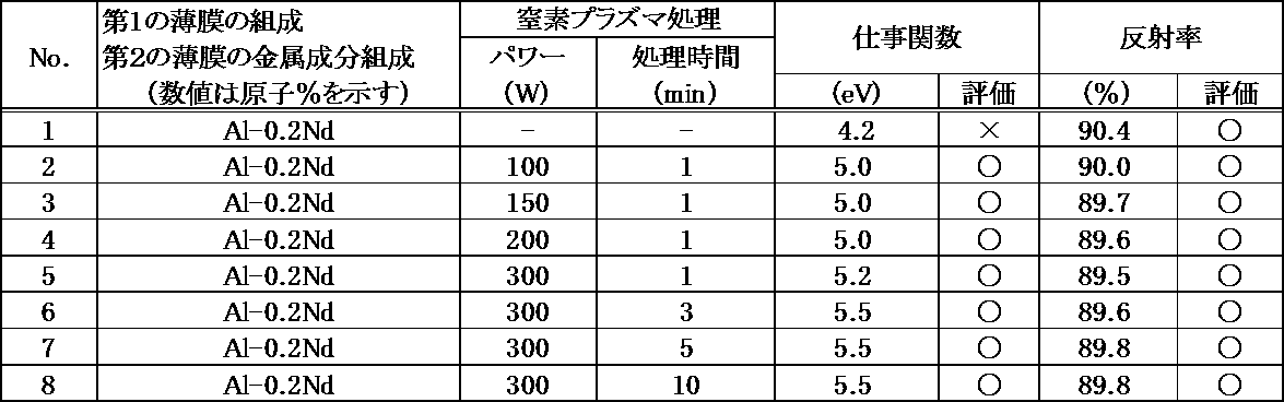
表2より次のように考察することができる。No.1は、本発明の第1の薄膜に該当するAl合金膜のみで、第2の薄膜(窒素含有Al合金膜)を有していないため、仕事関数が小さくなった。これに対しNo.2~8は、窒素プラズマ処理を行って第2の薄膜を形成したものであるが、いずれも所望の仕事関数と反射率が得られた。
本出願を詳細にまた特定の実施態様を参照して説明したが、本発明の精神と範囲を逸脱することなく様々な変更や修正を加えることができることは当業者にとって明らかである。
本出願は、2012年9月7日出願の日本特許出願(特願2012-197510)に基づくものであり、その内容はここに参照として取り込まれる。
本出願は、2012年9月7日出願の日本特許出願(特願2012-197510)に基づくものであり、その内容はここに参照として取り込まれる。
本発明によれば、純AlまたはAl合金からなる第1の薄膜と、窒素含有Alまたは窒素含有Al合金からなる第2の薄膜とのAl系積層膜で構成される反射電極が、高い反射率を示すと共に高い正孔注入特性を示すため、従来用いられてきた酸化物導電膜を含む反射電極に代えて、有機EL素子の反射電極に適用することができる。
その結果、本発明に係る反射電極の製造方法において、従来の反射電極(酸化物導電膜と金属膜の積層膜)のように異質の材料を積層させるのではなく、同一組成の材料を用いて形成できることから、発光輝度特性に優れた有機ELディスプレイや有機EL照明等を、生産性良く製造することができる。
1 基板
2 TFT
3 パシベーション膜
4 平坦化層
5 コンタクトホール
6 第1の薄膜(Al系膜)
7 第2の薄膜(窒素含有Al系膜)
8 有機層(有機発光層)
9 カソード電極
2 TFT
3 パシベーション膜
4 平坦化層
5 コンタクトホール
6 第1の薄膜(Al系膜)
7 第2の薄膜(窒素含有Al系膜)
8 有機層(有機発光層)
9 カソード電極
Claims (11)
- 基板と、反射電極と有機層の積層構造をこの順で含む有機EL素子であって、
前記反射電極は、前記基板側から順に、純AlまたはAl合金からなる第1の薄膜と、窒素含有Alまたは窒素含有Al合金からなる第2の薄膜とのAl系積層膜で構成され、かつ、前記第2の薄膜は前記有機層と直接接続していることを特徴とする有機EL素子。 - 前記第2の薄膜に含まれる窒素量は、30原子%以上50原子%以下である請求項1に記載の有機EL素子。
- 前記第2の薄膜の厚さは0.5nm以上10nm以下である請求項1に記載の有機EL素子。
- 前記第1の薄膜および前記第2の薄膜の少なくとも一方は、合金元素として、希土類元素を0.05~5原子%含有するものである請求項1に記載の有機EL素子。
- 前記希土類元素は、Nd,Gd,La,Y,Ce,PrおよびDyよりなる群から選択される1種類以上の元素である請求項4に記載の有機EL素子。
- 請求項1~5のいずれか一項に記載の有機EL素子の反射電極を製造する方法であって、
前記第1の薄膜を、不活性ガス中にてスパッタリング法で形成する工程、および、前記第2の薄膜を、不活性ガスと窒素ガスの混合ガス中にてスパッタリング法で形成する工程を含む有機EL素子の反射電極の製造方法。 - 請求項1~5のいずれか一項に記載の有機EL素子の反射電極を製造する方法であって、
前記第1の薄膜を、不活性ガス中にてスパッタリング法で形成する工程、および、前記第2の薄膜を、前記第1の薄膜の表面に窒素プラズマ処理を行って形成する工程を含む有機EL素子の反射電極の製造方法。 - 請求項1~5のいずれか一項に記載の有機EL素子の反射電極形成用Al合金スパッタリングターゲットであって、希土類元素を0.05~5原子%含有することを特徴とする有機EL素子の反射電極形成用Al合金スパッタリングターゲット。
- 前記希土類元素は、Nd,Gd,La,Y,Ce,PrおよびDyよりなる群から選択される1種類以上の元素である請求項8に記載のAl合金スパッタリングターゲット。
- 請求項1~5のいずれか一項に記載の有機EL素子を備えた有機ELディスプレイ。
- 請求項1~5のいずれか一項に記載の有機EL素子を備えた有機EL照明。
Applications Claiming Priority (2)
| Application Number | Priority Date | Filing Date | Title |
|---|---|---|---|
| JP2012-197510 | 2012-09-07 | ||
| JP2012197510A JP2014053191A (ja) | 2012-09-07 | 2012-09-07 | 有機EL素子、有機EL素子用反射電極の製造方法、および有機EL素子の反射電極形成用Al合金スパッタリングターゲット |
Publications (1)
| Publication Number | Publication Date |
|---|---|
| WO2014038560A1 true WO2014038560A1 (ja) | 2014-03-13 |
Family
ID=50237169
Family Applications (1)
| Application Number | Title | Priority Date | Filing Date |
|---|---|---|---|
| PCT/JP2013/073720 Ceased WO2014038560A1 (ja) | 2012-09-07 | 2013-09-03 | 有機EL素子、有機EL素子の反射電極の製造方法、および有機EL素子の反射電極形成用Al合金スパッタリングターゲット |
Country Status (3)
| Country | Link |
|---|---|
| JP (1) | JP2014053191A (ja) |
| TW (1) | TW201417373A (ja) |
| WO (1) | WO2014038560A1 (ja) |
Citations (4)
| Publication number | Priority date | Publication date | Assignee | Title |
|---|---|---|---|---|
| JP2000150172A (ja) * | 1998-11-12 | 2000-05-30 | Idemitsu Kosan Co Ltd | 有機el表示素子及びその製造方法 |
| JP2006236839A (ja) * | 2005-02-25 | 2006-09-07 | Mitsubishi Electric Corp | 有機電界発光型表示装置 |
| JP2010062067A (ja) * | 2008-09-05 | 2010-03-18 | Sony Corp | 表示装置の製造方法および表示装置 |
| JP2010135300A (ja) * | 2008-11-10 | 2010-06-17 | Kobe Steel Ltd | 有機elディスプレイ用の反射アノード電極およびその製造方法 |
-
2012
- 2012-09-07 JP JP2012197510A patent/JP2014053191A/ja active Pending
-
2013
- 2013-09-03 WO PCT/JP2013/073720 patent/WO2014038560A1/ja not_active Ceased
- 2013-09-06 TW TW102132196A patent/TW201417373A/zh unknown
Patent Citations (4)
| Publication number | Priority date | Publication date | Assignee | Title |
|---|---|---|---|---|
| JP2000150172A (ja) * | 1998-11-12 | 2000-05-30 | Idemitsu Kosan Co Ltd | 有機el表示素子及びその製造方法 |
| JP2006236839A (ja) * | 2005-02-25 | 2006-09-07 | Mitsubishi Electric Corp | 有機電界発光型表示装置 |
| JP2010062067A (ja) * | 2008-09-05 | 2010-03-18 | Sony Corp | 表示装置の製造方法および表示装置 |
| JP2010135300A (ja) * | 2008-11-10 | 2010-06-17 | Kobe Steel Ltd | 有機elディスプレイ用の反射アノード電極およびその製造方法 |
Also Published As
| Publication number | Publication date |
|---|---|
| JP2014053191A (ja) | 2014-03-20 |
| TW201417373A (zh) | 2014-05-01 |
Similar Documents
| Publication | Publication Date | Title |
|---|---|---|
| JP5235011B2 (ja) | 有機elディスプレイ用の反射アノード電極 | |
| KR101745290B1 (ko) | 반사 전극용 Ag 합금막 및 반사 전극 | |
| KR20110082040A (ko) | 유기 el 디스플레이용 반사 애노드 전극 및 그 제조 방법 | |
| WO2010053183A1 (ja) | 有機elディスプレイ用の反射アノード電極および配線膜 | |
| CN110463349B (zh) | 有机电致发光元件用电极、有机电致发光元件、有机电致发光显示装置和有机电致发光元件用电极的制造方法 | |
| WO2014080933A1 (ja) | 表示装置または入力装置に用いられる電極、および電極形成用スパッタリングターゲット | |
| KR102327851B1 (ko) | 유기 el 디스플레이용 반사 애노드 전극 | |
| CN103548420B (zh) | 含有有机el显示器用的反射阳极电极的配线结构 | |
| KR102196736B1 (ko) | 유기 el 디스플레이용 반사 애노드 전극 | |
| JP2012059470A (ja) | 有機elディスプレイ用の反射アノード電極 | |
| JP2014120487A (ja) | 表示装置または入力装置に用いられる電極、および電極形成用スパッタリングターゲット | |
| JP2012243742A (ja) | 有機elディスプレイ用の反射アノード電極を含む配線構造 | |
| WO2014038560A1 (ja) | 有機EL素子、有機EL素子の反射電極の製造方法、および有機EL素子の反射電極形成用Al合金スパッタリングターゲット | |
| JP6023404B2 (ja) | 有機elディスプレイ用の反射アノード電極を含む配線構造の製造方法 | |
| JP2014120486A (ja) | 表示装置または入力装置に用いられる電極、および電極形成用スパッタリングターゲット | |
| JP2014103312A (ja) | 表示装置または入力装置に用いられる電極、および電極形成用スパッタリングターゲット | |
| WO2015037582A1 (ja) | 有機el用反射電極膜、積層反射電極膜、及び、反射電極膜形成用スパッタリングターゲット | |
| JP2012243740A (ja) | 有機elディスプレイ用の反射アノード電極を含む配線構造 |
Legal Events
| Date | Code | Title | Description |
|---|---|---|---|
| 121 | Ep: the epo has been informed by wipo that ep was designated in this application |
Ref document number: 13835922 Country of ref document: EP Kind code of ref document: A1 |
|
| NENP | Non-entry into the national phase |
Ref country code: DE |
|
| 122 | Ep: pct application non-entry in european phase |
Ref document number: 13835922 Country of ref document: EP Kind code of ref document: A1 |