WO2014038237A1 - 表示方法及び表示装置 - Google Patents
表示方法及び表示装置 Download PDFInfo
- Publication number
- WO2014038237A1 WO2014038237A1 PCT/JP2013/060911 JP2013060911W WO2014038237A1 WO 2014038237 A1 WO2014038237 A1 WO 2014038237A1 JP 2013060911 W JP2013060911 W JP 2013060911W WO 2014038237 A1 WO2014038237 A1 WO 2014038237A1
- Authority
- WO
- WIPO (PCT)
- Prior art keywords
- light beam
- display
- transparent substrate
- display device
- display light
- Prior art date
Links
- 238000000034 method Methods 0.000 title claims abstract description 39
- 239000000758 substrate Substances 0.000 claims abstract description 194
- 230000004907 flux Effects 0.000 claims abstract description 25
- 230000003287 optical effect Effects 0.000 claims description 38
- 230000005540 biological transmission Effects 0.000 claims description 16
- 230000000644 propagated effect Effects 0.000 claims description 12
- 210000001747 pupil Anatomy 0.000 description 21
- 238000010586 diagram Methods 0.000 description 15
- 230000008569 process Effects 0.000 description 15
- 230000001427 coherent effect Effects 0.000 description 12
- 239000004973 liquid crystal related substance Substances 0.000 description 10
- 230000002411 adverse Effects 0.000 description 8
- 238000005286 illumination Methods 0.000 description 5
- 201000010041 presbyopia Diseases 0.000 description 5
- 230000004075 alteration Effects 0.000 description 4
- 238000006243 chemical reaction Methods 0.000 description 4
- 230000001902 propagating effect Effects 0.000 description 4
- 230000009471 action Effects 0.000 description 3
- 230000000694 effects Effects 0.000 description 2
- 230000008921 facial expression Effects 0.000 description 2
- 239000000853 adhesive Substances 0.000 description 1
- 230000001070 adhesive effect Effects 0.000 description 1
- 230000008859 change Effects 0.000 description 1
- 230000007423 decrease Effects 0.000 description 1
- 230000007246 mechanism Effects 0.000 description 1
- 230000009467 reduction Effects 0.000 description 1
- 239000004065 semiconductor Substances 0.000 description 1
- 229910052710 silicon Inorganic materials 0.000 description 1
- 239000010703 silicon Substances 0.000 description 1
- 230000001131 transforming effect Effects 0.000 description 1
Images


Classifications
-
- G—PHYSICS
- G03—PHOTOGRAPHY; CINEMATOGRAPHY; ANALOGOUS TECHNIQUES USING WAVES OTHER THAN OPTICAL WAVES; ELECTROGRAPHY; HOLOGRAPHY
- G03H—HOLOGRAPHIC PROCESSES OR APPARATUS
- G03H1/00—Holographic processes or apparatus using light, infrared or ultraviolet waves for obtaining holograms or for obtaining an image from them; Details peculiar thereto
- G03H1/04—Processes or apparatus for producing holograms
- G03H1/10—Processes or apparatus for producing holograms using modulated reference beam
- G03H1/12—Spatial modulation, e.g. ghost imaging
-
- G—PHYSICS
- G02—OPTICS
- G02B—OPTICAL ELEMENTS, SYSTEMS OR APPARATUS
- G02B27/00—Optical systems or apparatus not provided for by any of the groups G02B1/00 - G02B26/00, G02B30/00
- G02B27/10—Beam splitting or combining systems
- G02B27/1086—Beam splitting or combining systems operating by diffraction only
-
- G—PHYSICS
- G02—OPTICS
- G02B—OPTICAL ELEMENTS, SYSTEMS OR APPARATUS
- G02B5/00—Optical elements other than lenses
- G02B5/32—Holograms used as optical elements
-
- G—PHYSICS
- G02—OPTICS
- G02F—OPTICAL DEVICES OR ARRANGEMENTS FOR THE CONTROL OF LIGHT BY MODIFICATION OF THE OPTICAL PROPERTIES OF THE MEDIA OF THE ELEMENTS INVOLVED THEREIN; NON-LINEAR OPTICS; FREQUENCY-CHANGING OF LIGHT; OPTICAL LOGIC ELEMENTS; OPTICAL ANALOGUE/DIGITAL CONVERTERS
- G02F1/00—Devices or arrangements for the control of the intensity, colour, phase, polarisation or direction of light arriving from an independent light source, e.g. switching, gating or modulating; Non-linear optics
- G02F1/01—Devices or arrangements for the control of the intensity, colour, phase, polarisation or direction of light arriving from an independent light source, e.g. switching, gating or modulating; Non-linear optics for the control of the intensity, phase, polarisation or colour
- G02F1/13—Devices or arrangements for the control of the intensity, colour, phase, polarisation or direction of light arriving from an independent light source, e.g. switching, gating or modulating; Non-linear optics for the control of the intensity, phase, polarisation or colour based on liquid crystals, e.g. single liquid crystal display cells
- G02F1/133—Constructional arrangements; Operation of liquid crystal cells; Circuit arrangements
- G02F1/1333—Constructional arrangements; Manufacturing methods
- G02F1/1335—Structural association of cells with optical devices, e.g. polarisers or reflectors
- G02F1/133504—Diffusing, scattering, diffracting elements
-
- G—PHYSICS
- G03—PHOTOGRAPHY; CINEMATOGRAPHY; ANALOGOUS TECHNIQUES USING WAVES OTHER THAN OPTICAL WAVES; ELECTROGRAPHY; HOLOGRAPHY
- G03H—HOLOGRAPHIC PROCESSES OR APPARATUS
- G03H1/00—Holographic processes or apparatus using light, infrared or ultraviolet waves for obtaining holograms or for obtaining an image from them; Details peculiar thereto
- G03H1/04—Processes or apparatus for producing holograms
- G03H1/08—Synthesising holograms, i.e. holograms synthesized from objects or objects from holograms
- G03H1/0808—Methods of numerical synthesis, e.g. coherent ray tracing [CRT], diffraction specific
-
- G—PHYSICS
- G03—PHOTOGRAPHY; CINEMATOGRAPHY; ANALOGOUS TECHNIQUES USING WAVES OTHER THAN OPTICAL WAVES; ELECTROGRAPHY; HOLOGRAPHY
- G03H—HOLOGRAPHIC PROCESSES OR APPARATUS
- G03H1/00—Holographic processes or apparatus using light, infrared or ultraviolet waves for obtaining holograms or for obtaining an image from them; Details peculiar thereto
- G03H1/22—Processes or apparatus for obtaining an optical image from holograms
- G03H1/2202—Reconstruction geometries or arrangements
- G03H1/2205—Reconstruction geometries or arrangements using downstream optical component
-
- G—PHYSICS
- G03—PHOTOGRAPHY; CINEMATOGRAPHY; ANALOGOUS TECHNIQUES USING WAVES OTHER THAN OPTICAL WAVES; ELECTROGRAPHY; HOLOGRAPHY
- G03H—HOLOGRAPHIC PROCESSES OR APPARATUS
- G03H1/00—Holographic processes or apparatus using light, infrared or ultraviolet waves for obtaining holograms or for obtaining an image from them; Details peculiar thereto
- G03H1/22—Processes or apparatus for obtaining an optical image from holograms
- G03H1/2294—Addressing the hologram to an active spatial light modulator
-
- G—PHYSICS
- G03—PHOTOGRAPHY; CINEMATOGRAPHY; ANALOGOUS TECHNIQUES USING WAVES OTHER THAN OPTICAL WAVES; ELECTROGRAPHY; HOLOGRAPHY
- G03H—HOLOGRAPHIC PROCESSES OR APPARATUS
- G03H2222/00—Light sources or light beam properties
- G03H2222/20—Coherence of the light source
-
- G—PHYSICS
- G03—PHOTOGRAPHY; CINEMATOGRAPHY; ANALOGOUS TECHNIQUES USING WAVES OTHER THAN OPTICAL WAVES; ELECTROGRAPHY; HOLOGRAPHY
- G03H—HOLOGRAPHIC PROCESSES OR APPARATUS
- G03H2222/00—Light sources or light beam properties
- G03H2222/40—Particular irradiation beam not otherwise provided for
- G03H2222/46—Reconstruction beam at reconstruction stage
-
- G—PHYSICS
- G03—PHOTOGRAPHY; CINEMATOGRAPHY; ANALOGOUS TECHNIQUES USING WAVES OTHER THAN OPTICAL WAVES; ELECTROGRAPHY; HOLOGRAPHY
- G03H—HOLOGRAPHIC PROCESSES OR APPARATUS
- G03H2222/00—Light sources or light beam properties
- G03H2222/50—Geometrical property of the irradiating beam
- G03H2222/52—Divergent beam
-
- G—PHYSICS
- G03—PHOTOGRAPHY; CINEMATOGRAPHY; ANALOGOUS TECHNIQUES USING WAVES OTHER THAN OPTICAL WAVES; ELECTROGRAPHY; HOLOGRAPHY
- G03H—HOLOGRAPHIC PROCESSES OR APPARATUS
- G03H2222/00—Light sources or light beam properties
- G03H2222/50—Geometrical property of the irradiating beam
- G03H2222/53—Collimated beam
-
- G—PHYSICS
- G03—PHOTOGRAPHY; CINEMATOGRAPHY; ANALOGOUS TECHNIQUES USING WAVES OTHER THAN OPTICAL WAVES; ELECTROGRAPHY; HOLOGRAPHY
- G03H—HOLOGRAPHIC PROCESSES OR APPARATUS
- G03H2222/00—Light sources or light beam properties
- G03H2222/50—Geometrical property of the irradiating beam
- G03H2222/54—Convergent beam
-
- G—PHYSICS
- G03—PHOTOGRAPHY; CINEMATOGRAPHY; ANALOGOUS TECHNIQUES USING WAVES OTHER THAN OPTICAL WAVES; ELECTROGRAPHY; HOLOGRAPHY
- G03H—HOLOGRAPHIC PROCESSES OR APPARATUS
- G03H2223/00—Optical components
- G03H2223/16—Optical waveguide, e.g. optical fibre, rod
-
- G—PHYSICS
- G03—PHOTOGRAPHY; CINEMATOGRAPHY; ANALOGOUS TECHNIQUES USING WAVES OTHER THAN OPTICAL WAVES; ELECTROGRAPHY; HOLOGRAPHY
- G03H—HOLOGRAPHIC PROCESSES OR APPARATUS
- G03H2223/00—Optical components
- G03H2223/23—Diffractive element
-
- G—PHYSICS
- G03—PHOTOGRAPHY; CINEMATOGRAPHY; ANALOGOUS TECHNIQUES USING WAVES OTHER THAN OPTICAL WAVES; ELECTROGRAPHY; HOLOGRAPHY
- G03H—HOLOGRAPHIC PROCESSES OR APPARATUS
- G03H2225/00—Active addressable light modulator
- G03H2225/30—Modulation
- G03H2225/31—Amplitude only
-
- G—PHYSICS
- G03—PHOTOGRAPHY; CINEMATOGRAPHY; ANALOGOUS TECHNIQUES USING WAVES OTHER THAN OPTICAL WAVES; ELECTROGRAPHY; HOLOGRAPHY
- G03H—HOLOGRAPHIC PROCESSES OR APPARATUS
- G03H2225/00—Active addressable light modulator
- G03H2225/30—Modulation
- G03H2225/32—Phase only
Definitions
- the present invention relates to a display method and a display device.
- an image display device for forming a virtual image of a display screen in front of an observer.
- the display light beam is propagated inside the substrate by repeatedly reflecting the inner surface of the display light beam in a transparent substrate. Each time the display light beam undergoes internal reflection, a part of the display light beam is emitted outside the substrate. By doing so, in this image display device, display light beams are emitted from almost the entire surface of the substrate (Patent Document 1).
- a display light beam is emitted from the display screen of the liquid crystal display element.
- the display light beam emitted from the display screen is converted into a parallel light beam by the objective lens and is incident on a transparent substrate.
- the display light beam propagates in the transparent substrate while repeating internal reflection in the transparent substrate. At this time, a part of the display light beam is emitted from the substrate for every internal reflection.
- the display light beam is emitted from the entire surface of the transparent substrate.
- the diameter of the entire display light beam emitted from the transparent substrate is larger than the diameter of the light beam when incident on the transparent substrate.
- a display light beam emitted from a transparent substrate In order for an observer to observe a virtual image on the display screen, a display light beam emitted from a transparent substrate must be incident on the eye.
- the diameter of the display light beam emitted from the transparent substrate is large (thick). Therefore, the allowable range of eye alignment with respect to the display light beam (transparent substrate) is wider than that when the diameter of the display light beam is small (thin). As a result, the observer can easily observe the virtual image.
- the display light beam emitted from the transparent substrate is a parallel light beam. Therefore, the observer can observe a virtual image behind the transparent substrate. Moreover, since the display light flux is thick, the observer does not need to bring his eyes close to the display device. Note that the depth of the transparent substrate refers to a position opposite to the position of the observer with the transparent substrate interposed therebetween.
- a display light beam emitted from a display screen is converted into a parallel light beam by an objective lens.
- the display light beam includes an off-axis light beam in addition to the on-axis light beam, the off-axis light beam must also be converted into a parallel light beam with less aberration. Therefore, a plurality of lenses are necessary for the objective lens.
- the configuration (liquid crystal display element and objective lens) until a parallel light beam is obtained becomes large.
- the present invention has been made in view of such problems, and an object thereof is to provide a display method and a display device having high optical performance while being small and thin.
- the display method of the present invention includes: The display luminous flux is repeatedly reflected inside the transparent substrate and propagates. Each time the display light beam undergoes internal reflection, a part of the display light beam is emitted outside the transparent substrate, A display method for emitting display light from almost the entire surface of a transparent substrate, The display light beam is holographically formed.
- the display device of the present invention is A spatial phase modulation element for forming a display beam; A transparent substrate on which the display luminous flux is repeatedly reflected from the inner surface, and A branching unit that emits a part of the display light beam to the outside of the transparent substrate each time the display light beam undergoes internal reflection; It is characterized by having.
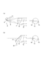
- FIG. 1A and 1B are diagrams showing a method and an apparatus for forming a display light beam 2 in a holographic manner, wherein FIG. 1A is a diagram showing a normal optical system for observing a virtual image, and FIG. It is a figure which shows a system
- FIG. 1A and 1B are diagrams illustrating a display device according to a first embodiment, in which FIG. 1A illustrates a case where a divergent light beam is incident on a transparent substrate, and FIG. 2B illustrates a case where a parallel light beam is incident on a transparent substrate.
- FIG. 1A illustrates a case where a divergent light beam is incident on a transparent substrate
- FIG. 2B illustrates a case where a parallel light beam is incident on a transparent substrate.
- a display light beam is formed in a holographic manner, and this display light beam is repeatedly reflected on the inner surface of the transparent substrate and propagated, and each time the inner surface is reflected, a part of the display light beam is removed from the transparent substrate. Inject and display. As the display light beam is propagated, a plurality of display light beams are emitted from the transparent substrate. In this way, the display light beam is emitted from almost the entire surface of the transparent substrate.
- the display light beam is formed holographically. Therefore, a display method having high optical performance can be realized while being small and thin.
- forming the display light beam in a holographic manner means forming (reproducing) the display light beam using a hologram.
- a plurality of display light beams are emitted from a transparent substrate as the display light beam is propagated.
- the observer can see the image by looking at any one display light beam or by viewing a plurality of display light beams. That is, it can be considered that the display light beams are combined to form one thick display light beam.
- the display beams are considered to be combined into one thick display beam. be able to.
- a plurality of display light beams are emitted from the transparent substrate, which is equivalent to one thick display light beam being emitted from the entire surface of the transparent substrate. Therefore, the entire surface of the transparent substrate is the exit pupil, and the size of the transparent substrate is the size of the exit pupil. Therefore, since the pupil is large like a loupe which is itself a pupil, an observer can easily observe a virtual image without bringing his face close to the display device.
- the display light beam emitted from the transparent substrate is a light beam for displaying a virtual image at infinity. That is, when the observer looks at the display light beam, a virtual image is formed at infinity (far). Therefore, for each of the plurality of display light beams emitted from the transparent substrate, a virtual image is formed at infinity when the observer views these display light beams. As a result, even if the observer's eyes are presbyopia that focuses only on the near point, the observer can see a focused display. In addition, the observer can see a virtual image formed at infinity regardless of which display light beam is viewed or a plurality of display light beams are viewed simultaneously.
- This display light beam (display light beam formed in a holographic manner) is parallel light.
- the display light beam is reflected, the reflected display light beam is amplitude-divided, and the light beam traveling in the same direction as the traveling direction of the reflected display light beam is reflected by the amplitude division.
- the display light beam may be a light beam generated by diffraction.
- FIG. 1 is a diagram showing the basic configuration of the display device of this embodiment and how the display light beam propagates.
- FIG. 1A shows a divergent light beam incident on a transparent substrate
- FIG. 1B shows a parallel light beam. The case where it injects into the transparent board
- the display device of this embodiment includes LCOS (Liquid Crystal On Silicon) 3, 3 ′, a transparent substrate 4, and a diffraction grating 5.
- LCOS 3 and 3 ′ are SPMs (Spatial Phase Modulators), which are hologram display elements that form the display light beam 2 in a holographic manner. Note that a transmissive liquid crystal display element can be used in place of the LCOSs 3 and 3 '.
- the transparent substrate 4 has an interface (first transmission surface) 4a and an interface (second transmission surface) 4b.
- the display light beam 2 is reflected (total reflection) on the inner surface thereof, that is, the interface 4 a or the interface 4 b. As a result, the display light beam 2 propagates inside the transparent substrate 4.
- the diffraction grating 5 is a branching means. Each time the display light beam 2 undergoes internal reflection, the diffraction grating 5 emits a part of the light beam to the outside of the transparent substrate 4.
- the diffraction grating 5 is located between the interface 4a and the interface 4b.
- the diffraction grating 5 is disposed so as to face the LCOSs 3 and 3 '.
- the diffraction grating 5 may be composed of a volume hologram.
- FIG. 1A shows a case where illumination light from a light source (not shown) is a divergent light beam.
- the divergent light beam 1 enters from the interface 4a and enters the LCOS 3 provided at the interface 4b.
- a phase hologram hologram pattern or phase pattern
- LCOS 3 phase hologram
- the display light beam 2 is generated as the first-order diffracted light (first-order light) of the hologram displayed on the LCOS 3.
- the 0th-order diffracted light (0th-order light) specularly reflected by the LCOS 3 is emitted from the transparent substrate 4.
- the phase hologram displayed on the LCOS 3 is a hologram that generates a parallel display light beam 2 when the divergent light beam 1 is incident.
- the display light beam 2 corresponds to an on-axis display light beam (light beam emitted from the center of the image).
- the off-axis display light beam (light beam emitted from other than the center of the image) is generated holographically from the LCOS 3, the off-axis display light beam is not shown.
- FIG. 1B shows a case where the illumination light from the light source (not shown) is a parallel light flux.
- the parallel light beam 1 ' enters from the interface 4a and enters the LCOS 3' provided at the interface 4b.
- LCOS 3 ' a phase hologram (hologram pattern or phase pattern) is displayed. Therefore, the illumination light incident on the LCOS 3 'is diffracted by the phase hologram (LCOS 3').
- the display light beam 2 is generated holographically from the LCOS 3 '.
- the display light beam 2 is generated as the first-order diffracted light (first-order light) of the hologram displayed on the LCOS 3 '.
- the 0th-order diffracted light (0th-order light) specularly reflected by the LCOS 3 ′ exits the transparent substrate 4.
- the phase hologram displayed on the LCOS 3 ' is a hologram that generates a parallel display light beam 2 when the parallel light beam 1' is incident.
- the display light beam 2 corresponds to an on-axis display light beam (light beam emitted from the center of the image).
- An off-axis display light beam (light beam emitted from other than the center of the image) is also generated holographically from the LCOS 3 ', but the off-axis display light beam is not shown.
- a convergent light beam may be incident on the LCOSs 3 and 3 '.
- a hologram that generates a parallel display light beam when the converged light beam is incident may be displayed on the LCOS 3, 3'.
- FIG. 2A is a diagram showing a normal optical system when observing a virtual image
- FIG. 2B is a diagram showing an optical system that forms a display light beam in a holographic manner.
- This display light beam is a light beam when the virtual image is observed (parallel light beams 10 and 12 in FIG. 2A).
- the optical system shown in FIG. 2A is composed of a display element 6 such as an LCD and a lens 7.
- a display element 6 such as an LCD
- a lens 7 When the display element 6 is placed at the focal position (front focal position) of the lens 7, the image 8 displayed on the display element 6 is projected at infinity by the lens 7.
- a solid line 9 is a light beam emitted from the center (on the axis) of the display element 6, and a broken line 11 is a light beam emitted from the end (off-axis) of the display element.
- the light beam indicated by the solid line 9 becomes a parallel light beam 10 and exits the lens 7. Further, the light beam indicated by the broken line 11 also becomes a parallel light beam 12 and exits the lens 7.
- the parallel light beams 10 and 12 enter the pupil 14 of the observer's eye 13. Thereby, the observer can see the image 15 of the image 8. Since the luminous fluxes 10 and 12 incident on the observer's pupil 14 are parallel luminous fluxes, the observer views a virtual image at the back of the display device (left side of the display element 6 in FIG. 2A), that is, at infinity. You are observing. Therefore, even if the observer's eyes are presbyopia whose focus is only at the near point, the observer can see the focused image 8.
- FIG. 2 (b) shows an optical system when the parallel light beams 10 and 12 are formed in a holographic manner.
- This optical system includes a coherent light source 16 and an SPM (spatial phase modulation element) 17.
- As the coherent light source 16 there is an LD (laser diode).
- the SPM 17 includes the LCOS described above.
- the SPM 17 is a hologram display element. In the future, the hologram display element will be referred to as SPM.
- the hologram has a hologram pattern.
- the hologram pattern is an interference pattern formed by two wavefronts.
- One wavefront is a wavefront emitted from the lens 7 in FIG. 2A
- the other wavefront is a wavefront emitted from the coherent light source 16 in FIG.
- the wavefronts (parallel light beams 10 and 12) emitted from the lens 7 include image information of the image 8.
- the wavefront emitted from the coherent light source 16 is a wavefront that generates interference fringes and at the same time is a wavefront that generates reproduction light from a hologram.
- the light emitted from the display element 6 is incoherent light. Therefore, even if the light emitted from the display element 6 and the wavefront emitted from the coherent light source 16 are overlapped, there is no interference. That is, a hologram pattern cannot be obtained. Therefore, in practice, a hologram (hologram pattern) is obtained by calculation. The calculated hologram is displayed on the SPM 17 and illuminated by the coherent light source 16. By doing so, holograms, that is, parallel light beams 10 and 12 are reproduced. The parallel light beam 10 out of the parallel light beams 10 and 12 is the display light beam 2 shown in FIG.
- the observer can observe the image 8 when the observer sees the parallel light beams 10 and 12 formed in the holographic manner. That is, the parallel light beams 10 and 12 are incident on the pupil 14 of the observer's eye 13 to form an image 15.
- the lens 7 needs to project an off-axis image (an image displayed on the periphery of the display element 6) onto the eye 13 with high resolution.
- the lens 7 is actually composed of a plurality of lenses.
- the diameter of the lens 7 needs to be increased. For this reason, when the optical system shown in FIG. 2A is used for the display device, it is difficult to reduce the thickness and size of the display device.
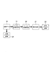
- FIG. 3 is a block diagram showing a process for obtaining a hologram by calculation.
- image data 18 is prepared.
- the image data 18 is data input to the display element 6 in FIG.
- the wavefront emitted from the lens 7 is obtained by Fourier transforming the image data 18 in the Fourier transform process 20.
- the spatial intensity distribution obtained by Fourier transform also causes a spatial intensity distribution at the same time as the spatial frequency distribution, a phase hologram with good diffraction efficiency cannot be formed. Therefore, a random phase is applied 19 before the Fourier transform process 20. If random phase information is given (superimposed) to the image data 18 in advance, the value of the spatial intensity after Fourier transform can be averaged over the entire spatial frequency plane, that is, the spatial intensity can be made substantially equal. As a result, the hologram can be a phase hologram having only phase information.
- This correction process 21 is a correction process based on the arrangement of the optical system.
- the hologram parallel light beams 10 and 12
- the correction process 21 calculates a hologram based on this spherical wave information. Thereafter, the calculation result (hologram information) is input to the SPM driver control 22. Then, a hologram is displayed on the SPM 17 (LCOS3, 3 'in FIG. 1) according to control information from the SPM driver control 22.
- the diffraction efficiency of the SPM 17 is almost constant, so that both bright scene images and dark scene images have the same brightness. Therefore, when the display light beam is formed holographically, it is necessary to control the amount of light incident on the SPM 17 according to the total amount of light of the image. Therefore, the brightness of the light source is controlled by inputting the total light amount data of the image data 18 to the light source driver 23.
- the display light beam 2 emitted from the LCOS 3 is totally reflected by the interface 4 a of the transparent substrate 4 and enters the diffraction grating 5.
- the diffraction grating 5 a part of the display light beam 2 is diffracted.
- the diffraction direction is the normal direction of the interface 4a.
- the light beam diffracted by the diffraction grating 5 exits from the transparent substrate 4 to become a display light beam 2a.
- the display light beam 2 transmitted through the diffraction grating 5 is further totally reflected by the interface 4 b of the transparent substrate 4 and passes through the diffraction grating 5.
- the display light beam 2 transmitted through the diffraction grating 5 is totally reflected again by the interface 4 a and enters the diffraction grating 5.
- a part of the display light beam 2 is diffracted.
- the diffraction direction is the normal direction of the interface 4a.
- the light beam diffracted by the diffraction grating 5 exits from the transparent substrate 4 to become a display light beam 2b.
- the display light beam 2 propagates through the transparent substrate 4 to form a new display light beam 2c.
- a large number of display light beams (2a, 2b, 2c) are emitted from the entire surface of the transparent substrate 4 (interface 4a).
- the observer can observe a virtual image by causing at least one of the display light beams 2a, 2b, and 2c to enter the eye.
- the observer can observe the moving image. If the image data is a still image, the observer can observe the still image.
- the display light beam 2 is formed using LCOS3. Therefore, a display device having high optical performance can be realized while being small and thin. Further, the light beam incident on the LCOS 3 may be only the axial light beam. For this reason, the light emitted from the light source can be used as a light beam incident on the LCOS 3 as it is. In this case, since a lens for light beam conversion is not required, the display device can be reduced in thickness and size.
- the display device can be reduced in thickness and size.
- the display light beam 2 is formed holographically by LCOS 3 and 3 ′. Therefore, as described above, the display device can be reduced in thickness and size.
- a plurality of display light beams 2a, 2b, and 2c are emitted from the transparent substrate 4 as the display light beam is propagated.
- the observer can observe a virtual image by causing at least one display light beam to enter the pupil of the eye.
- the display beam includes an on-axis beam that displays the center of the image and an off-axis beam that displays the edge of the image.
- Each display beam is thick, and the exit pupil is the entire surface of the transparent substrate from which the display beam is emitted. It becomes. Therefore, the permissible range of eye alignment with respect to the display light beam (transparent substrate 4) is wider than when the diameter of the display light beam is small (thin). As a result, the observer can easily observe the virtual image.
- LCOS or a transmissive liquid crystal display element is used for SPM, but a deformable mirror can also be used.
- deformable mirrors there are a type that deflects each of a plurality of micromirrors and a type that deforms one thin mirror.
- the display device can be manufactured as follows, for example. First, a concave portion is formed in a part of the transparent substrate 4, that is, a portion where the diffraction grating 5 is provided. And the diffraction grating 5 is arrange
- FIG. 4A shows a case where a divergent light beam is incident on a transparent substrate
- FIG. 4B shows a case where a parallel light beam is incident on a transparent substrate.
- LCOS reflection type liquid crystal display element
- SPM spatial phase modulation element
- the display device of the present embodiment includes a light source 24, LCOS (reflection type liquid crystal display elements) 3, 3 ', a transparent substrate 4, and a diffraction grating 5.
- LCOS reflection type liquid crystal display elements
- the transparent substrate 4 has an interface (first transmission surface) 4a and an interface (second transmission surface) 4b.
- the display light beam 2 is reflected (total reflection) on the inner surface thereof, that is, the interface 4 a or the interface 4 b. As a result, the display light beam 2 propagates inside the transparent substrate 4.
- LCOS 3 and 3 ′ are SPMs (spatial phase modulation elements), which are elements that form the display light beam 2.
- the diffraction grating 5 is a branching means. Each time the display light beam 2 undergoes internal reflection, the diffraction grating 5 emits a part of the light beam to the outside of the transparent substrate 4.
- the diffraction grating 5 is located between the interface 4a and the interface 4b.
- the diffraction grating 5 is disposed so as to face the LCOSs 3 and 3 '.
- the diffraction grating 5 may be constituted by a volume hologram. Further, when the transparent substrate 4 is viewed from the light source 24 side, the LCOSs 3 and 3 ′ and the diffraction grating 5 are arranged adjacent to each other.
- the display light beam 2 is emitted from the LCOSs 3 and 3 '. As described with reference to FIG. 1, the display light beam 2 propagates through the transparent substrate 4, and the display light beams 2 a, 2 b, and 2 c are emitted outside the transparent substrate 4. In the display device shown in FIG. 4B, the display light beams 2b and 2c are generated but are not shown.
- the LCOS 3 shown in FIG. 4A displays a hologram (phase hologram) in which a parallel display light beam 2 is generated when the divergent light beam 1 is incident. Therefore, the divergent light beam 1 emitted from the light source 24 can be directly incident on the LCOS 3 without conversion. As a result, the light source 24 can be brought close to the transparent substrate 4 or the LCOS 3. In FIG. 4A, the light source 24 is in contact with the interface 4a. Therefore, the display device can be reduced in thickness and size.
- a hologram phase hologram
- the light source 24 may be positioned closer to the interface 4b than the interface 4a.
- a recess hole may be formed from the interface 4a toward the inside of the transparent substrate 4, and the light source 24 may be disposed in the recess.
- the display device can be further reduced in thickness and size.
- the light source 24 may be disposed at a position slightly distant from the interface 4a (in the vicinity of the interface 4a) as long as it does not interfere with the reduction in thickness and size.
- the display device shown in FIG. 4A does not require a lens for light beam conversion, so that the display device can be reduced in thickness and size.
- the LCOS 3 ′ shown in FIG. 4B displays a hologram in which a parallel display light beam 2 is generated when the parallel light beam 1 ′ is incident. Therefore, the lens 25 is disposed in the optical path from the light source 24 to the LCOS 3 ′. The lens 25 converts the divergent light beam 1 into a parallel light beam 1 '.
- the display device shown in FIG. 4B since the lens 25 exists, it is difficult to arrange the light source 24 in the vicinity of the interface 4a. Therefore, it cannot be said that the display device is reduced in thickness and size as compared with the display device illustrated in FIG.
- the lens 25 can be simplified, for example, the number of lenses constituting the lens 25 can be reduced.
- a single lens is sufficient for the lens 25.
- the lens aberration may be corrected in the above-described correction process 21 (FIG. 3). Therefore, even when the light beam incident on the LCOS 3 ′ is a parallel light beam, the display device can be made thinner and smaller than the conventional display device (FIG. 2A).
- the LCOSs 3 and 3 ' may be arranged on the interface a side (between the interface a and the interface b) with respect to the interface b.
- the hologram information is corrected by the correction processing 21 (FIG. 3). By doing in this way, when the divergent light beam 1 is incident on the LCOS 3, an accurate display light beam 2 is formed.
- the hologram information displayed in the LCOS 3 ′ is corrected in the hologram information in the correction process 21 (FIG. 3). By doing so, an accurate display light beam 2 is formed when the parallel light beam 1 ′ is incident on the LCOS 3 ′.
- the 0th-order light (0th-order diffracted light) reflected by the LCOS 3 is emitted from the transparent substrate 4 while diverging, so that the display (observation of a virtual image) is adversely affected. There is nothing.
- the zero-order light reflected by the LCOS 3 ′ is emitted from the transparent substrate 4 as it is (in the state of a parallel light beam) as it is, which adversely affects the display (observation of a virtual image). Will not affect.
- the 0th-order light passes through the transparent substrate 4 and the primary light (display light beam 2) satisfies the condition of total reflection on the transparent substrate 4 (interfaces 4a and 4b). , LCOS3 and LCOS3 ′ are arranged. Therefore, the 0th order light does not adversely affect the display (observation of a virtual image).
- the light beam incident on the observer's pupil is a parallel light beam, so the observer observes a virtual image at the back of the display device, that is, at infinity. Therefore, even if the observer's eyes are presbyopia whose focus is only at the near point, the observer can see the focused image 8.
- the display device of the second embodiment is shown in FIG.
- the display device of the present embodiment has another LCOS 26 in the optical path from the light source 24 to the LCOS 3 ′.
- the LCOS 3 ' is arranged on the interface 4a side
- the LCOS 26 is arranged on the interface 4b side.
- the member which produces the same function as the display apparatus of 1st Embodiment attaches
- LCOS 3 displays a hologram that generates parallel display light beam 2 when parallel light beam 1' is incident.
- the LCOS 26 displays a hologram that generates a parallel light beam 1 'when the divergent light beam 1 is incident.
- the divergent light beam 1 emitted from the light source 24 enters the LCOS 26.
- the divergent light beam 1 is converted into a parallel light beam 1 ′ by the LCOS 26.
- the converted parallel light beam 1 ′ is emitted from the LCOS 26.
- the parallel light beam 1 ′ emitted from the LCOS 26 is incident on the LCOS 3 ′.
- the display light beam 2 is generated (reproduced) from the parallel light beam 1 ′, and the display light beam 2 is emitted from the LCOS 3 ′.
- the display light beam 2 propagates through the transparent substrate 4, and the display light beam 2 a (2 b, 2 c) is emitted outside the transparent substrate 4.
- the lens 25 must be disposed between the light source 24 and the interface 4a. Therefore, the light source 24 is arranged at a position away from the interface 4a. As a result, the display device cannot be sufficiently reduced in thickness and size.
- the LCOS 26 serving as the lens 25 can be arranged on the interface 4b side. Therefore, the light source 24 can be brought close to the interface 4a. As a result, the display device can be reduced in thickness and size to the same extent as the display device (first embodiment) shown in FIG.
- the LCOS 3 ′ and the diffraction grating 5 are arranged so as to overlap when the transparent substrate 4 is viewed from the light source 24 side. However, the LCOS 3 ′ and the diffraction grating 5 are actually arranged adjacent to each other so that the display light beam 2 a diffracted by the diffraction grating 5 does not pass through the LCOS 3 ′.
- the LCOS 26 can be replaced with a normal hologram (hologram lens). In this case, a volume hologram is preferable in terms of diffraction efficiency.
- FIG. 6 shows a display device according to the third embodiment.
- 6A shows a case where a divergent light beam is incident on a transparent substrate
- FIG. 6B shows a case where a parallel light beam is incident on a transparent substrate.
- an LCD transmission type liquid crystal display element
- SPM spatial phase modulation element
- the display device of this embodiment includes a light source 24, LCDs (transmission type liquid crystal display elements) 27 and 27 ', a transparent substrate 4, and a diffraction grating 5.
- the member which produces the same function as the display apparatus of 1st Embodiment attaches
- LCDs 27 and 27 ′ are SPMs (spatial phase modulation elements) and are elements that form the display light beam 2.
- the divergent light beam 1 from the light source 24 is incident on the LCD 27.
- the parallel light beam 1 'from the light source 24 is incident on the LCD 27'.
- the display light beam 2 is formed as the first-order diffracted light (primary light).
- the action of the display light beam 2 propagating through the transparent substrate 4 and the display light beams 2a, 2b, 2c exiting the transparent substrate 4 is the same as that of the display device of the first embodiment.
- the LCD 27 shown in FIG. 6A displays a hologram (phase hologram) that generates a parallel display light beam 2 when the diverging light beam 1 is incident. Therefore, the divergent light beam 1 emitted from the light source 24 can be directly incident on the LCD 27 without being converted. As a result, the light source 24 can be brought close to the transparent substrate 4 or the LCD 27. Therefore, the display device can be reduced in thickness and size.
- a hologram phase hologram
- the LCD 27 ′ shown in FIG. 4B displays a hologram that generates a parallel display light beam 2 when the parallel light beam 1 ′ is incident. Therefore, it is necessary to arrange a lens (not shown) in the optical path from the light source 24 to the LCD 27 '. However, only the axial light beam needs to enter the LCD 27 '. Therefore, the lens can be simplified, for example, the number of lenses constituting the lens can be reduced. In the display device shown in FIG. 4B, a single lens is sufficient. Further, the lens aberration may be corrected in the above-described correction process 21 (FIG. 3). Therefore, even when the light beam incident on the LCD 27 ′ is a parallel light beam, the display device can be made thinner and smaller than the conventional display device (FIG. 2A).
- the LCDs 27 and 27 ' may be disposed at a position slightly away from the interface b as long as the thickness and size are not affected.
- the LCDs 27 and 27 ′ may be arranged on the interface a side (between the interface a and the interface b) with respect to the interface b.
- the light source 24 and the LCDs 27 and 27 ' may be arranged on the interface a side.
- the hologram information displayed on the LCD 27 is subjected to hologram information correction processing in correction processing 21 (FIG. 3). By doing so, when the divergent light beam 1 enters the LCD 27, an accurate display light beam 2 is formed. Similarly, the hologram information displayed on the LCD 27 ′ is corrected in the hologram information in the correction process 21 (FIG. 3). By doing so, an accurate display light beam is formed when the parallel light beam 1 'is incident.
- the 0th-order light (0th-order diffracted light) transmitted through the LCD 27 is emitted from the transparent substrate 4 while diverging, so that the display (observation of a virtual image) is adversely affected. There is nothing.
- the 0th-order light 28 transmitted through the LCD 27 ′ is emitted from the vertically transparent substrate 4 as it is (in the state of a parallel light beam), so that it is displayed (observation of a virtual image). Will not be adversely affected.
- the 0th-order light passes through the transparent substrate 4 and the primary light (display light beam 2) satisfies the condition of total reflection on the transparent substrate 4 (interfaces 4a and 4b).
- LCD 27 and LCD 27 ' are arranged. Therefore, the 0th order light does not adversely affect the display (observation of a virtual image).
- the light beam incident on the observer's pupil is a parallel light beam, so the observer observes a virtual image at the back of the display device, that is, at infinity. Therefore, even if the observer's eyes are presbyopia whose focus is only at the near point, the observer can see the focused image 8.
- LCD which displays normal intensity
- it is not a phase hologram but an amplitude hologram that is displayed on the LCD, the diffraction efficiency is lowered.
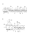
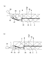
- FIGS. 7A is a diagram illustrating the configuration of the first transparent substrate and the state of propagation of the display light beam
- FIG. 7B is a diagram illustrating the configuration of the second transparent substrate and the state of propagation of the display light beam. is there.
- FIG. 8 is a diagram showing the overall configuration of the display device.
- the display device of this embodiment includes a first transparent substrate 30 and a second transparent substrate 36, as shown in FIG.
- the first transparent substrate 30 is located at the end of the second transparent substrate 36, and the first transparent substrate 30 is fixed to the second transparent substrate 36 at this position.
- the first transparent substrate 30 includes an SPM 29, a beam splitter 31, and a diffraction grating 32, as shown in FIG.
- the second transparent substrate 36 includes a beam splitter 37, a diffraction grating 38, and a diffraction grating 39, as shown in FIG. 7B.
- the diffraction grating 32, the diffraction grating 38, and the diffraction grating 39 are preferably volume holograms.
- the SPM 29 is a spatial phase modulation element that forms the display light beam 34 in a holographic manner. Further, on the first transparent substrate 30 and the second transparent substrate 36, the display light beam 34 is repeatedly reflected from the inner surface and propagated. Further, the beam splitter 31 causes a part of the display light beam 34 to be incident on the second transparent substrate 36 every time the display light beam 34 is internally reflected by the first transparent substrate 30. The beam splitter 37 causes a part of the display light beam 34 to be emitted from the second transparent substrate 36 every time the display light beam 34 is internally reflected by the second transparent substrate 36.
- the luminous flux (illumination light) and the display luminous flux incident on the display device show only the central ray of the axial luminous flux.
- a light beam it will be referred to as a light beam.
- the off-axis light beam is not clearly shown, it goes without saying that the off-axis light beam exists.
- the first transparent substrate 30 is made of a transparent member having a rectangular outer shape.
- An SPM 29, a beam splitter 31, and a diffraction grating 32 are arranged along the long side direction (X-axis direction).
- the display light beam 34 propagates along the long side direction.
- the thickness of the first transparent substrate 30 is 2 to 4 mm, for example.
- the outer shapes of the beam splitter 31 and the diffraction grating 32 are both rectangular. Further, the beam splitter 31 and the diffraction grating 32 are arranged to face each other. The beam splitter 31 is disposed between the two interfaces of the first transparent substrate 30. The diffraction grating 32 is disposed on one interface side of the first transparent substrate 30.
- a notch is formed at the end of this one interface.
- SPM29 is arrange
- one of the end surfaces (short side) sandwiched between the two interfaces is an inclined surface. From this inclined surface, a parallel light beam 33 enters.
- a parallel light beam 33 is incident on the SPM 29 from an LD light source (not shown).
- the display light beam 34 is formed as diffracted primary light by the hologram displayed on the SPM 29.
- the display light beam 34 is totally reflected on the inner surface (interface) of the first transparent substrate 30.
- the totally reflected display light beam 34 is separated into transmitted light and reflected light by the beam splitter 31.
- the transmitted light is incident on the diffraction grating 32 provided at the interface of the first transparent substrate 30. Then, it is diffracted by the diffraction grating 32 toward the beam splitter 31 side. The diffracted light becomes a display light beam 34a and exits the first transparent substrate 30 vertically.
- the display light beam 34a vertically emitted from the first transparent substrate 30 is incident on the second transparent substrate 36 (FIG. 7B).
- the reflected light is again totally reflected by the inner surface (interface) of the first transparent substrate 30 and enters the beam splitter 31 again. Then, the light is again separated into transmitted light and reflected light by the beam splitter 31.
- the reflected light separated again is totally reflected again by the inner surface (interface) of the first transparent substrate 30.
- the display light beam 34c is generated by the same action as the display light beam 34a and the display light beam 34b.
- the display light beam 34 repeats total reflection on the inner surface (interface) of the first transparent substrate 30 and propagates in the first transparent substrate 30. Then, while propagating, the display light beams 34 a, 34 b, 34 c are emitted vertically from the first transparent substrate 30 and incident on the second transparent substrate 36.
- the display light beams 34 a, 34 b, 34 c are emitted vertically from the first transparent substrate 30 and incident on the second transparent substrate 36.
- three display light beams to be emitted are shown (34a, 34b, 34c). The number of light beams is not limited to this.
- the diffraction grating 32 is preferably a volume hologram with high diffraction efficiency.
- the 0th-order light 35 specularly reflected by the SPM 29 is not totally reflected by the first transparent substrate 30 and is directly emitted to the outside of the first transparent substrate 30.
- the emitted zero-order light 35 is extinguished by a trap mechanism (not shown).
- the second transparent substrate 36 is made of a transparent member having a substantially rectangular outer shape.
- the length in the X-axis direction (short side) is the same as the length of the long side of the first transparent substrate 30.
- the length in the Z-axis direction (long side) is longer than the length of the short side of the first transparent substrate 30.
- the outer shape of the second transparent substrate 36 is not limited to a rectangle.
- the display light beam 34 propagates along the Z-axis direction. Note that the thickness of the second transparent substrate 36 is, for example, 2 to 4 mm.
- the outer shape of the diffraction grating 39 is rectangular like the diffraction grating 32. It is preferable that the length of the short side of the diffraction grating 39 does not exceed the length of the short side of the first transparent substrate 30.
- the diffraction grating 39 is disposed on one interface side of the second transparent substrate 36. Further, the diffraction grating 39 is disposed at a position facing the diffraction grating 32.
- Each of the beam splitter 37 and the diffraction grating 38 is provided in a range that does not overlap with the diffraction grating 39 (the first transparent substrate 30). Further, the beam splitter 37 and the diffraction grating 38 are arranged so as to face each other. The beam splitter 37 is disposed between the two interfaces of the second transparent substrate 36. The diffraction grating 38 is disposed on one interface of the second transparent substrate 36 (interface on which the diffraction grating 39 is disposed).
- the display light beams 34 a, 34 b, 34 c incident on the second transparent substrate 36 are diffracted by the diffraction grating 38.
- the diffracted display light beams 34 a, 34 b and 34 c are totally reflected by the inner surface (interface) of the second transparent substrate 36 and enter the beam splitter 37. From here on, explanation will be made using the display light beam 34a.
- the display light beam 34 a is separated into transmitted light and reflected light by a beam splitter 37.
- the transmitted light is incident on the diffraction grating 38. Then, it is diffracted by the diffraction grating 38 toward the beam splitter 37 side.
- the diffracted light becomes a display light beam 34d, and exits the second transparent substrate 36 vertically.
- the reflected light is totally reflected again by the inner surface (interface) of the second transparent substrate 36 and enters the beam splitter 37 again. Then, the light is again separated into transmitted light and reflected light by the beam splitter 37.
- the reflected light separated again is totally reflected again by the inner surface (interface) of the second transparent substrate 36.
- the display light beam 34f is generated by the same action as the display light beam 34d and the display light beam 34e.
- the display light beam 34a repeats total reflection on the inner surface (interface) of the second transparent substrate 36 and propagates through the second transparent substrate 36. Then, the display light beams 34d, 34e, and 34f are emitted vertically from the second transparent substrate 36 one after another while propagating. The same applies to the display light beams 34b and 34c. That is, as shown in FIG. 8, the display light beam 34 spreads in one direction 41 of the display device while propagating through the inside of the first transparent substrate 30 and is propagated through the inside of the second transparent substrate 36. It spreads in the other direction 42 of the display device. As a result, the display light beam 43 is emitted from the entire surface 40 of the display device.
- the SPM 29 displays a hologram that generates the parallel display light beam 34 when the parallel light beam 33 is incident. Therefore, it is necessary to arrange a lens (not shown) in the optical path from the light source to the SPM 29. However, only the axial light beam needs to enter the SPM 29. Therefore, the lens can be simplified, for example, the number of lenses constituting the lens can be reduced. In the display device of this embodiment, a single lens is sufficient as the lens. Further, the lens aberration may be corrected in the above-described correction process 21 (FIG. 3). Therefore, even when the light beam incident on the SPM 29 is a parallel light beam, the display device can be made thinner and smaller than the conventional display device (FIG. 2A).
- a divergent light beam may be incident on the SPM 29. Then, a hologram in which a parallel display light beam 34 is generated when a divergent light beam is incident on the SPM 29 may be displayed. In this way, the divergent light beam emitted from the light source can be directly incident on the SPM 29 without conversion. As a result, the light source can be brought closer to the transparent substrate 30 and the SPM 29. As a result, the display device can be reduced in thickness and size. Instead of the divergent light beam, a convergent light beam may be incident on the SPM 29.
- a plurality of display light beams 34d, 34e, and 34f are emitted from the second transparent substrate 36.
- the observer can see the image by looking at any one display light beam or by viewing a plurality of display light beams. That is, it can be considered that the display light beams are combined to form one thick display light beam.
- the display beams are considered to be combined into one thick display beam. be able to.
- a plurality of display light beams are emitted from the surface 40 of the display device.
- the entire surface 40 of the display device is the exit pupil
- the size of the surface 40 of the display device is the size of the exit pupil. Therefore, since the pupil is large like a loupe which is itself a pupil, an observer can easily observe a virtual image without bringing his face close to the display device.
- the display light beams 34d, 34e, and 34f (display light beam 43) emitted from the second transparent substrate 36 are light beams that display a virtual image at infinity. That is, when the observer looks at the display light beam, a virtual image is formed at infinity (far). Therefore, for each of the plurality of display light beams emitted from the second transparent substrate 36, a virtual image is formed at infinity when the observer views these display light beams. As a result, even if the observer's eyes are presbyopia that focuses only on the near point, the observer can see a focused display.
- a display device having a two-dimensional expansion can be obtained by using two transparent substrates.
- the surface on which the SPM 29 is arranged is inclined with respect to the surface on which the diffraction grating 32 is provided (FIG. 7A).
- Such a configuration is effective when the diffraction angle of the display light beam 34 emitted from the SPM 29 cannot be sufficiently large.
- this diffraction angle can be made sufficiently large, it is not necessary to incline the surface on which the SPM 29 is disposed with respect to the surface on which the diffraction grating 32 is provided. What is necessary is just to carry out similarly to the display apparatus of 1st-3rd embodiment.
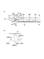
- FIG. 9A is a diagram illustrating a configuration of a first transparent substrate
- FIG. 9B is a diagram illustrating a relationship between incident light, diffracted light, and zeroth-order light.
- a hologram is displayed on the SPM (LCOS, LCD) 44.
- a hologram is a kind of diffraction grating. Therefore, as shown in FIG. 9B, the incident light (incident angle ⁇ R ) incident on the SPM 44 is diffracted at the diffraction angle ⁇ S. As a result, diffracted light is emitted from the SPM 44.
- the SPM 44 also emits zero-order light. This zero-order light is reflected by S at a reflection angle ⁇ R. Inject from PM44.
- the relationship between the incident angle ⁇ R , the diffraction angle ⁇ S and the pitch d of the diffraction grating is as follows. Note that ⁇ is the wavelength of incident light.
- the SPM 44 has a structure in which fine pixels are arranged one-dimensionally or two-dimensionally. A hologram is displayed using these fine pixels. Therefore, the size of two fine pixels, that is, twice the pixel pitch corresponds to the pitch d of the diffraction grating.
- the diffraction angle ⁇ S decreases as the pitch d of the diffraction grating increases, that is, as the pixel pitch of the SPM 44 increases.
- the reflection angle ⁇ R is constant, if the diffraction angle ⁇ S becomes small, it becomes difficult to separate the reflected light and the diffracted light.
- the surface on which the SPM 44 is arranged is inclined with respect to the surface on which the diffraction grating 32 is provided. In this way, it becomes easy to separate reflected light and diffracted light.
- the angle of view of the display device is ensured ⁇ 5.7 degrees.
- An angle of view of ⁇ 5.7 degrees is assumed when the display of a mobile device such as a mobile phone is viewed at a clear viewing distance. Since the field angle range is 11.4 degrees, the display light beam 34L (the off-axis principal ray of the display light beam (diffracted light or first-order diffracted light)) and the 0th order are separated in order to separate the display light beam 34 and the 0th order light 35.
- the angle difference with light needs to be at least 12 degrees.
- the angle formed between the display light beam 34 (the off-axis principal ray of the display light beam 34L) and the zero-order light 35 is 0.6 degrees, and the zero-order light 35 can be separated.
- the pixel pitch of the SPM 44 that displays the phase information is 3 ⁇ m. Then, the pitch of the diffraction grating (one state of the hologram) displayed on the SPM 44 is 6 ⁇ m.
- the incident angle ⁇ R is 60 degrees
- the diffraction angle ⁇ S is 72 degrees according to Equation 1. The required angle difference of 12 degrees can be secured.
- the display light beam 34 is incident on the inner surface (interface) of the transparent substrate 30 at an incident angle of 51.6 degrees and passes through the transparent substrate 30 with total reflection. Can propagate.
- FIG. 10 shows a display device of the fifth embodiment.
- (A) shows a case where the spatial phase modulation element is a reflection type
- (b) shows a case where the spatial phase modulation element is a transmission type.
- the display device of the present embodiment captures zero-order light emitted from the spatial phase modulation element.
- the member which produces the same function as the display apparatus of 1st Embodiment attaches
- the propagation of the display light beam 2 and the emission from the transparent substrate 4 are the same as those of the display device of the first embodiment.
- the divergent light beam 1 emitted from the light source 24 is converted into a convergent light beam 46 by the lens 45 and is incident on the LCOS 47.
- the display light beam 2 is formed by the phase hologram displayed on the LCOS 47.
- an inclined surface is formed at the end of the interface 4a. This inclined surface is inclined toward the interface 4b.
- a lens 45 is disposed on the inclined surface.
- An inclined surface is also formed at the end on the interface 4b side. This inclined surface is inclined toward the interface 4a.
- the LCOS 47 is disposed on this inclined surface.
- a trap 48 is provided at a position where an inclined surface is formed from the interface 4b.
- the trap 48 is formed vertically from the interface 4 b toward the diffraction grating 5.
- the display device shown in FIG. 10B is an example in which the divergent light beam 1 emitted from the light source 24 is converted into a convergent light beam 46 by the lens 45 and is incident on the LCD 47 '.
- the display light beam 2 is formed by the phase hologram displayed on the LCD 47 '.
- the lens 45 is disposed on the side surface sandwiched between the interface 4a and the interface 4b. Further, the LCD 47 'is disposed obliquely between the interface 4a and the interface 4b. The LCD 47 ′ is disposed between the lens 45 and the trap 48.
- the light source 24 is, for example, a semiconductor laser.
- a divergent light beam 1 is emitted from the light source 24.
- the divergent light beam 1 is converted into a convergent light beam 46 by the lens 45.
- the convergent light beam enters the LCOS 47 and the LCD 47 '. From the LCOS 47 and the LCD 47 ′, zero-order light and a display light beam 2 are generated.
- the LCOS 47 is a reflective SPM. Therefore, the 0th-order light regularly reflected by the LCOS 47 is directed to the trap 48.
- the LCD 47 ' is a transmissive SPM. Therefore, the 0th-order light that travels straight (transmits) through the LCD 47 ′ travels toward the trap 48.
- the trap 48 is a member that absorbs or blocks light. Therefore, the zero-order light incident on the trap 48 is absorbed or blocked by the trap 48. As a result, the zero-order light does not adversely affect the display light beam 2 (observation of a virtual image).
- the convergent light beam 46 is incident on the LCOS 47 or the LCD 47 '.
- the 0th order light emitted from the LCOS 47 and the LCD 47 ' is also a convergent light beam. Therefore, the 0th order light does not spread before entering the trap 48. As a result, the zero-order light does not adversely affect the display light flux 2.
- the beam diameter of the zero-order light at the position of the trap 48 is preferably smaller than the area of the trap 48, and if possible, it should be condensed in a dot shape.
- the lens 45 may be integrated with the transparent substrate 4.
- LCOS or a normal hologram may be used in place of the lens 45 in the same manner as in the display device of the second embodiment. In this way, the display device can be reduced in thickness and size.
- the LCD 47 ′ is integrally disposed in the transparent substrate 4. However, actually, for example, the LCD 47 ′ is sandwiched between two transparent members.
- the LCD 47 may be replaced with the LCD 47 ', and the LCD 47' may be covered with another transparent member from the LCD 47 'side.
- FIG. 11 is a diagram illustrating light beams emitted from the display device according to the present embodiment, and is a diagram illustrating optical distances of the respective light beams.
- a display device according to the fourth embodiment will be described as an example.
- a display light beam 43 is emitted from the surface 40 of the second transparent substrate 36 of the display device.
- the display light beam 43 is composed of display light beams 34d, 34e, and 34f (in practice, however, in addition to the three light beams, many light beams are emitted from the surface 40. Ejecting).
- a part of the display light beam enters the pupil 51 of the observer's eye, so that the observer can see the display (virtual image).
- FIG. 11 shows a state in which the display light beam is emitted from the three positions 50a, 50b, and 50c.
- Each of the three display light beams is composed of a display light beam 34, a most off-axis display light beam 34Uo, and a most off-axis display light beam 34Lo.
- the display light beam 34 corresponds to the light beam emitted from the axis (the center of the image).
- the most out-of-axis display light beam 34Uo corresponds to the light beam emitted from the most off-axis (one end of the image).
- the most off-axis display light beam 34Lo corresponds to the light beam emitted from the most off-axis (the other end of the image).
- 50a, 50b, and 50c are optical positions of the SPM 29 (FIG. 8) when viewed from the observer side. This optical position is the distance from the surface 40 of the second transparent substrate 36 to the SPM 29.
- Reference numeral 50a denotes an optical position of the SPM 29 when the display light beam 34 is totally reflected once in the second transparent substrate 36 and emitted.
- Reference numeral 50b denotes an optical position of the SPM 29 when the display light beam is totally reflected twice in the second transparent substrate 36 and emitted.
- Reference numeral 50c denotes an optical position of the SPM 29 when the display light beam is totally reflected three times within the second transparent substrate 36 and emitted.
- the optical distance difference 49 is a distance propagated by one total reflection that occurs in the second transparent substrate 36. More specifically, it is the distance when the display light beam 34 reciprocates from the beam splitter 37 to the interface.
- optical positions of the SPM 29 are actually the same as the number of light beams that propagate by repeating total reflection in two dimensions.
- display light beams from the SPM 29 at a plurality of different optical positions are normally incident on the observer's pupil.
- the display light beam 34, the most off-axis display light beam 34Lo, and the most off-axis display light beam 34Uo are formed holographically by coherent light. Therefore, the display light beam 34, the most off-axis display light beam 34Lo, and the most off-axis display light beam 34Uo are also coherent light.
- the display light beam (34, 34L, 34U) from 50b is mainly incident on the pupil 51 of the observer, but the display light beam from 50a and 50c is also incident depending on the position of the pupil 51. To do.
- the display light beam from 50a, the display light beam from 50b, and the display light beam from 50c are each coherent light. For this reason, when the display light beam from 50b and the display light beam from 50a enter the observer's pupil 51, the two light beams interfere with each other, and the virtual image to be observed becomes an unintended image (virtual image). It is done.
- An unintended image is, for example, an image with degraded image quality.
- the coherence length of the light source 24 is preferably shorter than the difference 49 of the optical distance. That is, the coherence length of the light source 24 is preferably shorter than the distance propagated by one total reflection that occurs in the second transparent substrate 36. By doing so, it is possible to prevent an unintended image from being formed even when a plurality of display light beams having different optical distances enter the observer's eyes.
- SPM is used to generate a display light beam holographically.
- the display light beam can be generated holographically without using SPM.
- a hologram pattern may be recorded on the film, and this film may be disposed at the SPM position.
- the film may not be a film as long as it has a characteristic that the hologram pattern can be recorded only once.
- the display method and display device according to the present invention are useful in that they have high optical performance while being small and thin.
Abstract
表示方法は、表示光束2が透明な基板内4を繰り返し内面反射して伝播し、表示光束が内面反射を行う毎に、表示光束の一部を透明な基板4外に射出することにより、透明な基板4のほぼ全面から表示光束を射出する表示方法であって、表示光束をホログラフィックに形成する、あるいは、表示装置は、表示光束を形成する空間位相変調素子3と、表示光束が繰り返し内面反射して伝播する透明な基板4と、表示光束が内面反射を行う毎に、表示光束2の一部を透明な基板外4へ射出させる分岐手段5と、を有する。
Description
本発明は、表示方法及び表示装置に関する。
近年、表示画面の虚像を観察者の前方に形成するための画像表示装置が提案されている。この画像表示装置では、表示光束を透明な基板内で繰り返し内面反射させて、表示光束を基板内で伝播させている。そして、表示光束が内面反射を行う毎に、その表示光束の一部を基板外に射出させている。このようにすることにより、この画像表示装置では、基板のほぼ全面から表示光束を射出させている(特許文献1)。
より具体的には、この画像表示装置では、液晶表示素子の表示画面から表示光束が射出する。表示画面から射出した表示光束は対物レンズで平行光束に変換されて、透明な基板に入射する。そして、表示光束は透明な基板内で内面反射を繰り返しながら、透明な基板内を伝播する。このとき、内面反射毎に、表示光束の一部が基板から外に射出する。このように、透明な基板の複数の位置から表示光束が射出するため、透明な基板全面から表示光束が射出する。その結果、透明な基板から射出する表示光束全体の径は、透明な基板に入射したときの光束の径よりも大きくなる。
観察者が表示画面の虚像を観察するためには、透明な基板から射出する表示光束を眼に入射させなくてならない。上記の画像表示装置では、透明な基板から射出する表示光束の径が大きい(太い)。そのため、表示光束(透明な基板)に対する眼の位置合わせの許容範囲は、表示光束の径が小さい(細い)場合と比べると広くなる。その結果、観察者は、容易に虚像を観察することができる。
また、透明な基板から射出する表示光束は平行光束である。そのため、観察者は透明な基板の奥に虚像を観察することができる。また、表示光束が太いので、観察者は表示装置に眼を近づける必要が無い。なお、透明な基板の奥とは、透明な基板を挟んで観察者の位置と反対側の位置のことである。
特許文献1の画像表示装置では、表示画面(液晶表示素子)から射出した表示光束を、対物レンズで平行光束に変換している。ここで、表示光束には、軸上光束に加えて軸外光束が含まれているので、軸外光束も収差の少ない平行光束に変換しなければならない。そのため、対物レンズには複数枚のレンズが必要となる。その結果、特許文献1の画像表示装置では、平行光束を得るまでの構成(液晶表示素子と対物レンズ)が大型化してしまう。
本発明は、このような課題に鑑みてなされたものであって、小型・薄型でありながら、高い光学性能を有する表示方法及び表示装置を提供することを目的とする。
上述した課題を解決し、目的を達成するために、本発明の表示方法は、
表示光束が透明な基板内を繰り返し内面反射して伝播し、
表示光束が内面反射を行う毎に、表示光束の一部を透明な基板外に射出することにより、
透明な基板のほぼ全面から表示光束を射出する表示方法であって、
表示光束をホログラフィックに形成することを特徴とする。
表示光束が透明な基板内を繰り返し内面反射して伝播し、
表示光束が内面反射を行う毎に、表示光束の一部を透明な基板外に射出することにより、
透明な基板のほぼ全面から表示光束を射出する表示方法であって、
表示光束をホログラフィックに形成することを特徴とする。
また、本発明の表示装置は、
表示光束を形成する空間位相変調素子と、
表示光束が繰り返し内面反射して伝播する透明な基板と、
表示光束が内面反射を行う毎に、表示光束の一部を透明な基板外へ射出させる分岐手段と、
を有することを特徴とする。
表示光束を形成する空間位相変調素子と、
表示光束が繰り返し内面反射して伝播する透明な基板と、
表示光束が内面反射を行う毎に、表示光束の一部を透明な基板外へ射出させる分岐手段と、
を有することを特徴とする。
本発明によれば、小型・薄型でありながら、高い光学性能を有する表示方法及び表示装置を提供することができる。
本発明のある態様にかかる実施形態の作用効果を説明する。なお、本実施形態の作用効果を具体的に説明するに際しては、具体的な例を示して説明することになる。しかし、それらの例示される態様はあくまでも本発明に含まれる態様のうちの一部に過ぎず、その態様には数多くのバリエーションが存在する。したがって、本発明は例示される態様に限定されるものではない。
本実施形態の表示方法は、表示光束をホログラフィックに形成し、この表示光束を透明な基板内を繰り返し内面反射させて伝播させ、内面反射する毎に表示光束の一部を透明な基板の外に射出して表示を行う。そして、表示光束が伝播されるに従って、複数の表示光束が透明な基板から射出される。このようにすることで、透明な基板のほぼ全面から表示光束を射出させている。
本実施形態の表示方法では、表示光束をホログラフィックに形成している。そのため、小型・薄型でありながら、高い光学性能を有する表示方法が実現できる。なお、表示光束をホログラフィックに形成するとは、ホログラムを使って表示光束を形成(再生)することを意味している。
また、本実施形態の表示方法では、表示光束が伝播されるに従って、複数の表示光束が透明な基板から射出される。観察者は、いずれか1つの表示光束を見ても、或いは複数の表示光束を見ても像を見ることができる。すなわち、それぞれの表示光束が合わさって一つの太い表示光束となっているとみなすことができる。また、画像の中心を表示する軸上の表示光束だけでなく、画像の端を表示する軸外の表示光束も同様に、それぞれの表示光束が合わさって一つの太い表示光束となっているとみなすことができる。このように、本実施形態の表示方法では、透明な基板から複数の表示光束が射出するが、これは、透明な基板の全面から一つの太い表示光束が射出されているのと等価である。そのため、透明な基板の全面が射出瞳であり、また、透明な基板の大きさが射出瞳の大きさである。従って、それ自体が瞳であるルーペと同様に瞳が大きいので、観察者は表示装置に顔を近づけなくても容易に虚像を観察することができる。
また、本実施形態の表示方法では、透明な基板から外に射出される表示光束は、無限遠に虚像を表示する光束である。すなわち、観察者が表示光束を見た時、無限遠(遠方)に虚像が形成される。よって、透明な基板から射出された複数の表示光束の各々についても、観察者がこれらの表示光束を見た時、全て無限遠に虚像が形成される。その結果、観察者の目が近点にしか焦点の合わない老眼であっても、観察者は焦点の合った表示を見ることができる。また、観察者はどの表示光束を見ても、或いは複数の表示光束を同時に見ても、無限遠に形成された虚像を見ることができる。なお、この表示光束(ホログラフィックに形成された表示光束)は平行光である。
また、本実施形態の表示方法は、表示光束を反射させ、反射させた表示光束を振幅分割し、振幅分割によって、反射させた表示光束の進行方向と同じ方向に進行する光束と、反射させた表示光束の進行方向と異なる方向に進行する光束と、を生成し、反射と振幅分割を繰り返し行なう表示方法であって、表示光束は回折によって生成した光束であっても良い。
次に、本実施形態の表示装置の基本構成について説明する。図1は、本実施形態の表示装置の基本構成と表示光束の伝搬の様子を示す図であって、(a)は発散光束を透明な基板に入射させた場合、(b)は平行光束を透明な基板に入射させた場合を示している。
図1に示すように、本実施形態の表示装置は、LCOS(Liquid Crystal On Silicon:反射型液晶表示素子)3、3’と、透明な基板4と、回折格子5と、を有する。LCOS3、3’はSPM(Spacial Phase Modulator:空間位相変調素子)であって、表示光束2をホログラフィックに形成するホログラム表示素子である。なお、LCOS3、3’の代わりに、透過型の液晶表示素子を用いることもできる。
透明な基板4は界面(第1透過面)4aと、界面(第2透過面)4bと、を有する。透明な基板4では、その内面、すなわち、界面4aや界面4bで表示光束2の反射(全反射)が生じる。これにより、表示光束2は透明な基板4の内部を伝搬する。
回折格子5は分岐手段である。回折格子5は、表示光束2が内面反射を行う毎に、その光束の一部を透明な基板4の外へ射出させる。回折格子5は、界面4aから界面4bまでの間に位置している。また、回折格子5は、LCOS3、3’と対向するように配置されている。なお、この回折格子5は、ボリュームホログラムで構成されていても良い。
表示光束2を形成するためには、LCOS3、3’に照明光を入射させる必要がある。図1(a)は、光源(不図示)からの照明光が発散光束の場合を示している。発散光束1は、界面4aから入射し、界面4bに設けられたLCOS3に入射する。ここで、LCOS3には位相ホログラム(ホログラムパターン、あるいは位相パターン)が表示されている。そのため、LCOS3に入射した発散光束1は位相ホログラム(LCOS3)で回折される。その結果、LCOS3から、表示光束2がホログラフィックに生成される。なお、表示光束2は、LCOS3に表示されたホログラムの1次回折光(1次光)として生成される。LCOS3で正反射した0次回折光(0次光)は、透明な基板4を射出する。
図1(a)の表示装置では、LCOS3に表示させている位相ホログラムが、発散光束1を入射させたときに平行な表示光束2を生じるホログラムとなっている。また、表示光束2は軸上の表示光束(画像の中心から出た光束)に相当する。なお、LCOS3からは軸外の表示光束(画像の中心以外から出た光束)もホログラフィックに生成されるが、軸外の表示光束については図示を省略している。
一方、図1(b)は、光源(不図示)からの照明光が平行光束の場合を示している。平行光束1’は、界面4aから入射し、界面4bに設けられたLCOS3’に入射する。LCOS3’では位相ホログラム(ホログラムパターン、あるいは位相パターン)が表示されている。そのため、LCOS3’に入射した照明光は位相ホログラム(LCOS3’)で回折される。その結果、LCOS3’から、表示光束2がホログラフィックに生成される。なお、表示光束2は、LCOS3’に表示されたホログラムの1次回折光(1次光)として生成される。LCOS3’で正反射した0次回折光(0次光)は、透明な基板4を射出する。
図1(b)の表示装置では、LCOS3’に表示させている位相ホログラムが、平行光束1’を入射させたときに平行な表示光束2を生じるホログラムとなっている。また、表示光束2は軸上の表示光束(画像の中心から出た光束)に相当する。LCOS3’からは軸外の表示光束(画像の中心以外から出た光束)もホログラフィックに生成されるが、軸外の表示光束については図示を省略している。
なお、LCOS3、3’には、発散光束や平行光束のほかに、収束光束を入射させても良い。LCOS3、3’に収束光束を入射させる場合は、収束光束を入射させたときに平行な表示光束が生じるホログラムを、LCOS3、3’に表示させれば良い。
ここで、表示光束2をホログラフィックに形成する方法及び装置について、図2を用いて詳説する。図2において、(a)は虚像を観察するときの通常の光学系を示す図、(b)は表示光束をホログラフィックに形成する光学系を示す図である。この表示光束は、虚像を観察するときの光束(図2(a)における平行光束10、12)である。
図2(a)に示す光学系は、LCDなどの表示素子6と、レンズ7と、で構成されている。表示素子6をレンズ7の焦点位置(前側焦点位置)に置くと、表示素子6に表示された画像8はレンズ7によって無限遠に投影される。ここで、実線9は表示素子6の中心(軸上)から射出する光束、破線11は表示素子の端(軸外)から射出する光束である。実線9で示す光束は、平行光束10となってレンズ7を射出する。また、破線11で示す光束も、平行光束12となってレンズ7を射出する。
平行光束10と12は、観察者の眼13の瞳14に入射する。これにより、観察者は画像8の像15を見ることができる。観察者の瞳14に入射する光束10と12は平行光束であるので、観察者は表示装置の奥(図2(a)において、表示素子6よりも左側)、すなわち、無限遠にある虚像を観察していることになる。したがって、観察者の目が近点にしか焦点の合わない老眼であっても、観察者は焦点の合った画像8を見ることができる。
図2(b)は、平行光束10、12をホログラフィックに形成するときの光学系を示している。この光学系は、コヒーレント光源16と、SPM(空間位相変調素子)17と、で構成されている。コヒーレント光源16としては、LD(レーザーダイオード)がある。また、SPM17としては、前述のLCOSがある。なお、このSPM17は、ホログラム表示素子のことである。今後は、ホログラム表示素子をSPMと称する。
ホログラムはホログラムパターンを有する。ホログラムパターンは、2つの波面によって形成された干渉パターンである。1つの波面は、図2(a)のレンズ7から射出する波面で、もう1つの波面は、図2(b)のコヒーレント光源16から射出する波面である。ここで、レンズ7から射出する波面(平行光束10、12)は、画像8の像の情報を含んでいる。一方、コヒーレント光源16から射出する波面は干渉縞を生成する波面であると同時に、ホログラムから再生光を生成するための波面である。
なお、表示素子6から射出する光はインコヒーレントな光である。そのため、表示素子6から射出する光と、コヒーレント光源16から射出する波面と、を重ね合わせても干渉しない。すなわち、ホログラムパターンを得ることができない。そこで、実際には、計算でホログラム(ホログラムパターン)を求める。そして、計算したホログラムをSPM17に表示し、コヒーレント光源16で照明する。このようにすることで、ホログラム、すなわち、平行光束10、12が再生される。平行光束10、12のうちの平行光束10が、図1に示す表示光束2である。
そして、このホログラフィックに形成された平行光束10、12を観察者が見ることによって、観察者は画像8を観察することができる。すなわち、平行光束10、12は観察者の眼13の瞳14に入射し、像15を形成する。
なお、図2(a)に示す光学系では、レンズ7は、軸外の画像(表示素子6の周辺部に表示された画像)も解像力良く眼13に投影する必要がある。そのために、実際には、レンズ7は複数枚のレンズで構成される。また、レンズ7は、その径も大きくする必要がある。このようなことから、表示装置に図2(a)に示す光学系を用いた場合、表示装置の薄型化・小型化は困難となる。
次に、計算によるホログラムの求め方を詳説する。図3は、計算によってホログラムを求めるときの処理を示すブロック図である。図3に示すように、まず、画像データ18を用意する。この画像データ18は、図2(a)において、表示素子6に入力されるデータである。レンズ7から射出する波面は、フーリエ変換処理20で、画像データ18をフーリエ変換することによって求められる。
ただし、フーリエ変換によって求められた空間周波数分布には、空間位相分布と同時に空間強度分布も生じるので、回折効率の良い位相ホログラムを形成できない。そこで、フーリエ変換処理20の前に、ランダム位相の付与19が行われる。予め画像データ18にランダムな位相情報を付与(重畳)しておくと、フーリエ変換後の空間強度の値を空間周波数面全面に渡って平均化、すなわち、空間強度をほぼ等しくするができる。その結果、ホログラムを位相情報のみを持つ位相ホログラムとすることができる。
次に補正処理21を行う。この補正処理21は、光学系の配置に基づく補正処理である。例えば、図2(b)に示す光学系では、コヒーレント光源16からの波面でホログラム(平行光束10、12)を再生する。この再生を行なったときに、正確な表示光束2(平行光束10、12)が形成されるようにする必要がある。コヒーレント光源16からの波面は球面波であるので、補正処理21では、この球面波の情報でホログラムを計算する。その後、計算結果(ホログラム情報)はSPMドライバ制御22に入力される。そして、SPMドライバ制御22からの制御情報により、SPM17(図1ではLCOS3、3’)にホログラムが表示される。
なお、SPM17の回折効率はほぼ一定であるので、明るいシーンの画像でも、暗いシーンの画像でも、同程度の明るさになってしまう。従って、表示光束をホログラフィックに形成する場合は、画像の総光量に従ってSPM17に入射させる光量を制御する必要がある。そこで、画像データ18の総光量データを光源ドライバ23に入力することで、光源の明るさの制御が行われる。
図1(a)に戻って説明を続ける。LCOS3から射出した表示光束2は、透明な基板4の界面4aで全反射し、回折格子5に入射する。回折格子5では、表示光束2の一部が回折される。回折方向は、界面4aの法線方向である。回折格子5で回折された光束は透明な基板4から外に射出し、表示光束2aとなる。
回折格子5を透過した表示光束2は、更に透明な基板4の界面4bで全反射し、回折格子5を透過する。回折格子5を透過した表示光束2は、再び界面4aで全反射し、回折格子5に入射する。回折格子5では、表示光束2の一部が回折される。回折方向は、界面4aの法線方向である。回折格子5で回折された光束は透明な基板4から外に射出し、表示光束2bとなる。同様に、表示光束2は透明な基板4内を伝播し、新たな表示光束2cを形成する。このような繰り返しにより、透明な基板4(界面4a)の全面から多数の表示光束(2a、2b、2c)が射出される。
観察者は、表示光束2a、2b、2cの少なくとも1つを眼に入射させることで、虚像を観察することができる。ここで、例えば、画像データ18が動画の場合は、観察者は動画を観察することができる。また、画像データが静止画の場合は、観察者は静止画を観察することができる。
本実施形態の表示装置の基本構成では、LCOS3を用いて表示光束2を形成している。そのため、小型・薄型でありながら、高い光学性能を有する表示装置が実現できる。また、LCOS3に入射させる光束は軸上光束のみで良い。そのため、光源から射出した光を、そのままLCOS3に入射させる光束として使うことができる。この場合、光束変換用のレンズを必要としないため、表示装置の薄型化・小型化ができる。
また、LCOS3’に入射させる光束が平行光束の場合であっても、平行な軸上光束のみをLCOS3’に入射させればよい。そのため、収束光束や発散光束を平行光束に変換するレンズを、簡素化することができる。よって、LCOS3’に入射させる光束が平行光束の場合であっても、表示装置の薄型化・小型化ができる。
また、本実施形態の表示装置の基本構成では、LCOS3、3’で表示光束2をホログラフィックに形成している。そのため、上記のように、表示装置の薄型化・小型化ができる。
また、本実施形態の表示装置の基本構成では、表示光束が伝播されるに従って、複数の表示光束2a、2b、2cが透明な基板4から射出される。観察者は、眼の瞳に少なくとも1つの表示光束を入射させることで、虚像を観察することができる。本実施形態の表示装置の基本構成では、複数の表示光束2a、2b、2cが存在するので、表示光束の径が大きくなっているのと等価である。表示光束には画像の中心を表示する軸上光束と画像の端を表示する軸外光束があるが、それぞれの表示光束が太くなっており、射出瞳は表示光束が射出する透明な基板の全面となる。そのため、表示光束(透明な基板4)に対する眼の位置合わせの許容範囲は、表示光束の径が小さい(細い)場合比べると広くなる。その結果、観察者は、容易に虚像を観察することができる。
なお、上記のように、SPMには、LCOSや透過型の液晶表示素子が用いられるが、デフォーマブルミラーを用いることもできる。デフォーマブルミラーとしては、複数の微小ミラーの各々を偏向させるタイプや、1枚の薄いミラーを変形させるタイプがある。
また、表示装置は、例えば、次のようにして製作することができる。まず、透明な基板4の一部、すなわち、回折格子5を設ける部分に凹部を形成しておく。そして、この凹部に、回折格子5を配置する。その後、回折格子の上から、凹部と略一致する透明部材で覆う。あるいは、まず、透明な基板4の側面に、界面4aと平行なスリット状の凹部を形成する。そして、この凹部に回折格子5を挿入する。その後、側面を透明部材や接着材等で覆う。
第1実施形態の表示装置を図4に示す。図4において、(a)は発散光束を透明な基板に入射させた場合、(b)は平行光束を透明な基板に入射させた場合を示している。本実施形態の表示装置では、SPM(空間位相変調素子)として、LCOS(反射型液晶表示素子)3、3’を用いている。
本実施形態の表示装置は、光源24と、LCOS(反射型液晶表示素子)3、3’と、透明な基板4と、回折格子5と、を有する。なお、図1に示した表示装置と同様の機能を生じる部材は同じ番号を付し、説明は省略する。
透明な基板4は、界面(第1透過面)4aと、界面(第2透過面)4bと、を有する。透明な基板4では、その内面、すなわち、界面4aや界面4bで表示光束2の反射(全反射)が生じる。これにより、表示光束2は透明な基板4の内部を伝搬する。
LCOS3、3’はSPM(空間位相変調素子)であって、表示光束2を形成する素子である。このLCOS3、3’は、表示光束2をホログラフィックに形成するホログラム表示素子である。LCOS3、3’は、光源24から界面4bまでの間に配置されている。より具体的には、LCOS3、3’は、界面4bの空気と接触している側に設けられている。
回折格子5は分岐手段である。回折格子5は、表示光束2が内面反射を行う毎に、その光束の一部を透明な基板4の外へ射出させる。回折格子5は、界面4aから界面4bまでの間に位置している。また、回折格子5は、LCOS3、3’と対向するように配置されている。なお、この回折格子5は、ボリュームホログラムで構成しても良い。また、光源24側から透明な基板4を見たとき、LCOS3、3’と回折格子5とが隣り合うように配置されている。
このような構成において、LCOS3、3’から、表示光束2が射出される。そして、図1で説明したように、表示光束2は透明な基板4内を伝搬し、表示光束2a、2b、2cを透明な基板4の外に射出する。なお、図4(b)に示す表示装置でも表示光束2b、2cは生成されているが、図示を省略している。
図4(a)に示すLCOS3には、発散光束1を入射させたときに平行な表示光束2が生じるホログラム(位相ホログラム)が表示されている。そのため、光源24から射出した発散光束1を変換することなく、そのままLCOS3に入射させることができる。その結果、光源24を透明な基板4やLCOS3に近づけることができる。図4(a)では、光源24は界面4aに接している。よって、表示装置の薄型化・小型化ができる。
また、光源24は、界面4aよりも界面4b側に位置させても良い。例えば、界面4aから透明な基板4の内部に向けて凹部(穴)を形成し、凹部に光源24を配置しても良い。このようにすれば、表示装置をさらに薄型化・小型化ができる。なお、薄型化・小型化に支障のない範囲であれば、光源24を、界面4aからやや離れた位置(界面4aの近傍)に配置しても良い。
このように、図4(a)に示す表示装置では、光束変換用のレンズを必要としないため、表示装置の薄型化・小型化ができる。
一方、図4(b)に示すLCOS3’には、平行光束1’を入射させたときに平行な表示光束2が生じるホログラムが表示されている。そのため、光源24からLCOS3’までの光路中に、レンズ25が配置されている。このレンズ25により、発散光束1を平行光束1’に変換している。図4(b)示す表示装置では、レンズ25が存在するため、光源24を界面4aの近傍に配置することは難しい。よって、図4(a)に示す表示装置に比べると、表示装置が薄型化・小型化されているとはいえない。
しかしながら、図4(b)示す表示装置では、軸上光束のみをLCOS3’に入射させればよい。そのため、レンズ25を簡素化、例えば、レンズ25を構成するレンズの枚数を少なくすることができる。図4(b)示す表示装置では、レンズ25は単レンズで十分である。また、レンズの収差は、前述の補正処理21(図3)の中で補正すればよい。よって、LCOS3’に入射させる光束が平行光束の場合であっても、従来の表示装置(図2(a))に比べると表示装置の薄型化・小型化ができる。
なお、図4(a)や(b)示す表示装置において、LCOS3、3’を、界面bよりも界面a側(界面aと界面bの間)に配置しても良い。
また、LCOS3で表示するホログラムについては、補正処理21(図3)で、ホログラム情報の補正処理を行っている。このようにすることで、発散光束1がLCOS3に入射したときに、正確な表示光束2が形成される。同様に、LCOS3’で表示するホログラムについても、補正処理21(図3)で、ホログラム情報の補正処理を行っている。このようにすることで、平行光束1’がLCOS3’入射したときに、正確な表示光束2が形成される。
また、図4(a)に示す表示装置では、LCOS3で反射した0次光(0次の回折光)は発散しながら透明な基板4から射出するので、表示(虚像の観察)に悪影響を及ぼすことは無い。また、図4(b)に表示装置では、LCOS3’で反射した0次光は、そのまま(平行光束の状態で)、垂直に透明な基板4から射出するので、表示(虚像の観察)に悪影響を及ぼすことは無い。
また、本実施形態の表示装置では、0次光は透明な基板4を透過し、1次光(表示光束2)は透明な基板4(界面4a、4b)で全反射する条件を満たすように、LCOS3とLCOS3’が配置されている。よって、0次光が表示(虚像の観察)に悪影響を及ぼすことは無い。
また、本実施形態の表示装置でも、観察者の瞳に入射する光束は平行光束であるので、観察者は表示装置の奥、すなわち、無限遠にある虚像を観察していることになる。したがって、観察者の目が近点にしか焦点の合わない老眼であっても、観察者は焦点の合った画像8を見ることができる。
また、本実施形態の表示装置では、簡単のために、表示光束2については軸上光束のみを示し、軸外光束は明示していない。しかしながら、軸外光束が存在するのは言うまでもない。
第2実施形態の表示装置を図5に示す。本実施形態の表示装置は、光源24から、LCOS3’に至るまでの光路中に、別のLCOS26を有する。具体的には、図5に示すように、LCOS3’は界面4a側に配置され、LCOS26が界面4b側に配置されている。なお、第1実施形態の表示装置と同様の機能を生じる部材は同じ番号を付し、説明は省略する。
LCOS3’には、平行光束1’を入射させたときに平行な表示光束2が生じるホログラムが表示されている。一方、LCOS26には、発散光束1を入射させたときに平行光束1’が生じるホログラムが表示されている。
光源24から射出した発散光束1は、LCOS26に入射する。発散光束1は、LCOS26で平行光束1’に変換される。変換された平行光束1’は、LCOS26から射出する。LCOS26から射出した平行光束1’は、LCOS3’に入射する。LCOS3’では、平行光束1’から表示光束2が生成(再生)され、表示光束2はLCOS3’から射出する。そして、図1で説明したように、表示光束2は透明な基板4内を伝搬し、表示光束2a(2b、2c)を透明な基板4の外に射出する。
図4(b)に示す表示装置(第1実施形態)の場合、光源24と界面4aの間にレンズ25を配置しなくてはならない。そのため、光源24は、界面4aから離れた位置に配置される。その結果、表示装置の薄型化・小型化が十分にできない。
これに対して、本実施形態の表示装置では、レンズ25の役目を果たすLCOS26を、界面4b側に配置できる。そのため、光源24を、界面4aに接近させることができる。その結果、図4(a)に示す表示装置(第1実施形態)と同程度に、表示装置の薄型化・小型化ができる。
なお、図5では、光源24側から透明な基板4を見たとき、LCOS3’と回折格子5とが重なり合うように配置されている。しかしながら、回折格子5で回折された表示光束2aがLCOS3’を通過しないように、実際には、LCOS3’と回折格子5とは隣り合うように配置されている。
また、本実施形態では、簡単のために、表示光束2については軸上光束のみを示し、軸外光束は明示していない。しかしながら、軸外光束が存在するのは言うまでもない。また、LCOS26を通常のホログラム(ホログラムレンズ)で置き換えることもできる。この場合は、ボリュームホログラムが回折効率の点で好ましい。
第3実施形態の表示装置を図6に示す。図6において、(a)は発散光束を透明な基板に入射させた場合、(b)は平行光束を透明な基板に入射させた場合を示している。本実施形態の表示装置では、SPM(空間位相変調素子)として、LCD(透過型液晶表示素子)を用いている。
本実施形態の表示装置は、光源24と、LCD(透過型液晶表示素子)27、27’と、透明な基板4と、回折格子5と、を有する。なお、第1実施形態の表示装置と同様の機能を生じる部材は同じ番号を付し、説明は省略する。
LCD27、27’はSPM(空間位相変調素子)であって、表示光束2を形成する素子である。このLCDS27、27’は、表示光束2をホログラフィックに形成するホログラム表示素子である。LCD27、27’は、光源24から界面4bまでの間に配置されている。より具体的には、LCD27、27’は、界面4bの空気と接触している側に設けられている。
図6(a)に示す表情装置では、光源24からの発散光束1をLCD27に入射させる。一方、図6(b)に示す表情装置では、光源24からの平行光束1’をLCD27’に入射させる。そして、LCD27、27’に位相ホログラムを表示することにより、1次の回折光(1次光)として表示光束2を形成する。表示光束2が透明な基板4を伝播し、表示光束2a、2b、2cが透明な基板4を射出する作用は、第1実施形態の表示装置と同様である。
図6(a)に示すLCD27には、発散光束1を入射させたときに平行な表示光束2が生じるホログラム(位相ホログラム)が表示されている。そのため、光源24から射出した発散光束1を変換することなく、そのままLCD27に入射させることができる。その結果、光源24を透明な基板4やLCD27に近づけることができる。よって、表示装置の薄型化・小型化ができる。
一方、図4(b)に示すLCD27’には、平行光束1’を入射させたときに平行な表示光束2が生じるホログラムが表示されている。そのため、光源24からLCD27’までの光路中に、レンズ(不図示)を配置する必要がある。しかしながら、軸上光束のみをLCD27’に入射させればよい。そのため、レンズを簡素化、例えば、レンズを構成するレンズの枚数を少なくすることができる。図4(b)に示す表示装置では、レンズは単レンズで十分である。また、レンズの収差は、前述の補正処理21(図3)の中で補正すればよい。よって、LCD27’に入射させる光束が平行光束の場合であっても、従来の表示装置(図2(a))に比べると表示装置の薄型化・小型化ができる。
なお、薄型化・小型化に支障のない範囲であれば、図6(a)や(b)示す表示装置において、LCD27、27’を界面bからやや離れた位置に配置しても良い。あるいは、LCD27、27’を界面bよりも界面a側(界面aと界面bの間)に配置しても良い。また、光源24とLCD27、27’を、界面a側に配置しても良い。
また、第1実施形態の表示装置と同様に、LCD27で表示するホログラムについては、補正処理21(図3)で、ホログラム情報の補正処理を行っている。このようにすることで、発散光束1がLCD27に入射したときに、正確な表示光束2が形成される。同様に、LCD27’で表示するホログラムについても、補正処理21(図3)で、ホログラム情報の補正処理を行っている。このようにすることで、平行光束1’が入射したときに、正確な表示光束が形成される。
また、図6(a)に示す表示装置では、LCD27を透過した0次光(0次の回折光)は発散しながら透明な基板4から射出するので、表示(虚像の観察)に悪影響を及ぼすことは無い。また、図6(b)に示す表示装置では、LCD27’を透過した0次光28は、そのまま(平行光束の状態で)、垂直に透明な基板4から射出するので、表示(虚像の観察)に悪影響を及ぼすことは無い。
また、本実施形態の表示装置では、0次光は透明な基板4を透過し、1次光(表示光束2)は透明な基板4(界面4a、4b)で全反射する条件を満たすように、LCD27とLCD27’が配置されている。よって、0次光が表示(虚像の観察)に悪影響を及ぼすことは無い。
また、本実施形態の表示装置でも、観察者の瞳に入射する光束は平行光束であるので、観察者は表示装置の奥、すなわち、無限遠にある虚像を観察していることになる。したがって、観察者の目が近点にしか焦点の合わない老眼であっても、観察者は焦点の合った画像8を見ることができる。
なお、LCD27、27’に通常の強度情報を表示するLCDを用いても良い。この場合、LCDに表示されるのは位相ホログラムではなく、振幅ホログラムとなるので、回折効率は低下する。
また、本実施形態の表示装置では、簡単のために、表示光束2については軸上光束のみを示し、軸外光束は明示していない。しかしながら、軸外光束が存在するのは言うまでもない。
第4実施形態の表示装置を図7、図8に示す。図7において、(a)は第1の透明な基板の構成と表示光束の伝搬の様子を示す図、(b)は第2の透明な基板の構成と表示光束の伝搬の様子を示す図である。また、図8は、表示装置の全体構成を示す図である。
本実施形態の表示装置は、図8に示すように、第1の透明な基板30と、第2の透明な基板36と、を備える。第1の透明な基板30は第2の透明な基板36の端部に位置し、この位置で、第1の透明な基板30が第2の透明な基板36に固定されている。
第1の透明な基板30は、図7(a)に示すように、SPM29と、ビームスプリッタ31と、回折格子32と、を有する。また、第2の透明な基板36は、図7(b)に示すように、ビームスプリッタ37と、回折格子38と、回折格子39と、を有する。なお、回折格子32、回折格子38及び回折格子39は、ボリュームホログラムであることが好ましい。
SPM29は、表示光束34をホログラフィックに形成する空間位相変調素子である。また、第1の透明な基板30と第2の透明な基板36では、表示光束34が繰り返し内面反射して伝播する。また、ビームスプリッタ31は、表示光束34が第1の透明な基板30で内面反射を行う毎に、表示光束34の一部を第2の透明な基板36に入射させる。また、ビームスプリッタ37は、表示光束34が第2の透明な基板36で内面反射を行う毎に、表示光束34の一部を第2の透明な基板36から射出させる。
以下、詳細に説明する。なお、図7及び図8では、簡単のために、表示装置に入射させる光束(照明光)と表示光束は、軸上光束のうちの中心光線のみを示している。ただし、以下の説明では光束と称して説明する。また、軸外光束を明示していないが、軸外光束が存在するのは言うまでもない。
第1の透明な基板30は、図7(a)と及び図8に示すように、外形が長方形の透明部材で構成されている。そして、長辺方向(X軸方向)に沿って、SPM29、ビームスプリッタ31及び回折格子32が配置されている。表示光束34は、長辺方向に沿って伝播していく。なお、第1の透明な基板30の厚みは、例えば、2~4mmである。
ビームスプリッタ31と回折格子32の外形は、共に長方形となっている。また、ビームスプリッタ31と回折格子32は、対向するように配置されている。ビームスプリッタ31は、第1の透明な基板30の2つの界面の間に配置されている。回折格子32は、第1の透明な基板30の一方の界面側に配置されている。
また、この一方の界面の端部には、切り欠きが形成されている。そして、切り欠きによって生じた傾斜面に、SPM29が配置されている。また、2つの界面に挟まれた端面(短辺側)の1つは、傾斜面となっている。この傾斜面から、平行光束33が入射する。
本実施形態の表示装置では、図示しないLD光源から、平行光束33をSPM29に入射させている。そして、SPM29に表示されたホログラムにより、表示光束34が回折の1次光として形成される。表示光束34は、第1の透明な基板30の内面(界面)で全反射する。全反射した表示光束34は、ビームスプリッタ31で透過光と反射光に分離される。
透過光は、第1の透明な基板30の界面に設けられた回折格子32に入射する。そして、回折格子32によって、ビームスプリッタ31側に向かって回折される。回折された光は表示光束34aとなって、第1の透明な基板30を垂直に射出する。第1の透明な基板30を垂直に射出した表示光束34aは、第2の透明な基板36に入射する(図7(b))。
反射光は、再び第1の透明な基板30の内面(界面)で全反射され、再度ビームスプリッタ31に入射する。そして、ビームスプリッタ31で再度、透過光と反射光に分離される。
再度分離された透過光は、回折格子32に入射する。そして、回折格子32によって、ビームスプリッタ31側に向かって回折される。回折された光は表示光束34bとなって、第1の透明な基板30を垂直に射出する。第1の透明な基板30を垂直に射出した表示光束34bは、第2の透明な基板36に入射する(図7(b))。
再度分離された反射光は、再び、第1の透明な基板30の内面(界面)で全反射される。そして、表示光束34aや表示光束34bと同様の作用によって、表示光束34cが生成される。
このように、表示光束34は第1の透明な基板30の内面(界面)で全反射を繰り返して、第1の透明な基板30内を伝播する。そして、伝播しながら、次々と表示光束34a、34b、34cを第1の透明な基板30から垂直に射出させ、第2の透明な基板36に入射させる。なお、ここでは簡単の為に、射出する表示光束は三つ示している(34a、34b、34c)。光束の数はこれに限らない。
なお、回折格子32は、回折効率の高いボリュームホログラムが望ましい。また、SPM29で正反射した0次光35は第1の透明な基板30で全反射せず、そのまま第1の透明な基板30の外に射出する。そして、射出した0次光35は、図示しないトラップ機構により消滅する。
第2の透明な基板36は、図7(b)及び図8に示すように、外形が略長方形の透明部材で構成されている。X軸方向(短辺)の長さは、第1の透明な基板30の長辺の長さと同じである。一方、Z軸方向(長辺)の長さは、第1の透明な基板30の短辺の長さよりも長い。なお、第2の透明な基板36の外形は、長方形に限られない。表示光束34は、Z軸方向に沿って伝播していく。なお、第2の透明な基板36の厚みは、例えば、2~4mmである。
回折格子39の外形は、回折格子32と同様に長方形である。回折格子39の短辺の長さは、第1の透明な基板30の短辺の長さを超えないことが好ましい。回折格子39は、第2の透明な基板36の一方の界面側に配置されている。また、回折格子39は、回折格子32と対向する位置に配置されている。
ビームスプリッタ37と回折格子38の各々は、回折格子39(第1の透明な基板30)と重複していない範囲に設けられている。また、ビームスプリッタ37と回折格子38は、対向するように配置されている。ビームスプリッタ37は、第2の透明な基板36の2つの界面の間に配置されている。回折格子38は、第2の透明な基板36の一方の界面(回折格子39が配置されている界面)に配置されている。
第2の透明な基板36に入射した表示光束34a、34b、34cは、回折格子38により回折される。回折された表示光束34a、34b、34cは、第2の透明な基板36の内面(界面)で全反射してビームスプリッタ37に入射する。ここからは、表示光束34aを使って説明する。
表示光束34aは、ビームスプリッタ37で透過光と反射光に分離される。透過光は回折格子38に入射する。そして、回折格子38によって、ビームスプリッタ37側に向かって回折される。回折された光は表示光束34dとなって、第2の透明な基板36を垂直に射出する。
反射光は、再び第2の透明な基板36の内面(界面)で全反射され、再度ビームスプリッタ37に入射する。そして、ビームスプリッタ37で再度、透過光と反射光に分離される。
再度分離された透過光は、回折格子38に入射する。そして、回折格子38によって、ビームスプリッタ37側に向かって回折される。回折された光は表示光束34eとなって、第2の透明な基板36を垂直に射出する。
再度分離された反射光は、再び、第2の透明な基板36の内面(界面)で全反射される。そして、表示光束34dや表示光束34eと同様の作用によって、表示光束34fが生成される。
このように、表示光束34aは第2の透明な基板36の内面(界面)で全反射を繰り返して、第2の透明な基板36内を伝播する。そして、伝播しながら、次々と表示光束34d、34e、34fを第2の透明な基板36から垂直に射出させる。表示光束34b、34cも同様である。すなわち、図8に示すように、表示光束34は第1の透明な基板30の内部を伝播しながら表示装置の一方の方向41に広がると共に、第2の透明な基板36の内部を伝播しながら表示装置の他方の方向42に広がる。その結果、表示装置の表面40の全面から、表示光束43が射出される。
このように、本実施形態の表示装置では、SPM29には、平行光束33を入射させたときに平行な表示光束34が生じるホログラムが表示されている。そのため、光源からSPM29までの光路中に、レンズ(不図示)を配置する必要がある。しかしながら、SPM29には、軸上光束のみを入射させればよい。そのため、レンズを簡素化、例えば、レンズを構成するレンズの枚数を少なくすることができる。本実施形態の表示装置では、レンズは単レンズで十分である。また、レンズの収差は、前述の補正処理21(図3)の中で補正すればよい。よって、SPM29に入射させる光束が平行光束の場合であっても、従来の表示装置(図2(a))に比べると表示装置の薄型化・小型化ができる。
なお、SPM29に、発散光束を入射させても良い。そして、SPM29に、発散光束を入射させたときに平行な表示光束34が生じるホログラムを表示するようにしても良い。このようにすれば、光源から射出した発散光束を変換することなく、そのままSPM29に入射させることができる。その結果、光源を透明な基板30やSPM29に近づけることができる。その結果、表示装置の薄型化・小型化ができる。なお、発散光束に代えて、収束光束をSPM29に入射させても良い。
また、本実施形態の表示装置では、表示光束が伝播されるに従って、複数の表示光束34d、34e、34fが第2の透明な基板36から射出される。観察者は、いずれか1つの表示光束を見ても、或いは複数の表示光束を見ても像を見ることができる。すなわち、それぞれの表示光束が合わさって一つの太い表示光束となっているとみなすことができる。また、画像の中心を表示する軸上の表示光束だけでなく、画像の端を表示する軸外の表示光束も同様に、それぞれの表示光束が合わさって一つの太い表示光束となっているとみなすことができる。このように、本実施形態の表示装置では、表示装置の表面40から複数の表示光束が射出するが、これは、表示装置の表面40の全面から一つの太い表示光束が射出されているのと等価である。そのため、表示装置の表面40の全面が射出瞳であり、また、表示装置の表面40の大きさが射出瞳その大きさである。従って、それ自体が瞳であるルーペと同様に瞳が大きいので、観察者は表示装置に顔を近づけなくても容易に虚像を観察することができる。
また、第2の透明な基板36から外に射出される表示光束34d、34e、34f(表示光束43)は、無限遠に虚像を表示する光束である。すなわち、観察者が表示光束を見た時、無限遠(遠方)に虚像が形成される。よって、第2の透明な基板36から射出された複数の表示光束の各々についても、観察者がこれらの表示光束を見た時、全て無限遠に虚像が形成される。その結果、観察者の目が近点にしか焦点の合わない老眼であっても、観察者は焦点の合った表示を見ることができる。また、観察者はどの表示光束を見ても、或いは複数の表示光束を同時に見ても、無限遠に形成された虚像を見ることができる。なお、第1~3実施形態においても透明な基板を二枚用いて二次元的広がりのある表示装置に出来ることは言うまでもない。
さて、本実施形態の表示装置では、SPM29を配置した面を、回折格子32を設けた面に対して傾斜させている(図7(a))。このような構成は、SPM29から射出される表示光束34の回折角が十分に大きくとれない場合に有効である。しかしながら、この回折角を十分に大きく取れる場合は、SPM29を配置した面を、回折格子32を設けた面に対して傾ける必要はない。第1~3実施形態の表示装置と同様にすれば良い。
SPMから射出される表示光束の回折角が大きくとれない場合について、図9を用いて説明する。図9において、(a)は第1の透明な基板の構成を示す図、(b)は入射光、回折光及び0次光の関係を示す図である。なお、図7(a)と同様の機能を生じる部材は同じ番号を付し、説明は省略する。
上記のように、SPM(LCOS、LCD)44にはホログラムが表示される。ホログラムは、一種の回折格子である。そのため、図9(b)に示すように、SPM44に入射した入射光(入射角θR)は、回折角θSで回折される。その結果、SPM44から回折光が射出する。なお、SPM44からは0次光も射出する。この0次光は、反射角θRでS
PM44から射出する。
PM44から射出する。
ここで、入射角θR、回折角θS及び回折格子のピッチdの関係は、以下のようになる。なお、λは入射光の波長である。

SPM44は、微細な画素が1次元、あるいは2次元に配列された構造を持つ。この微細な画素を使ってホログラムを表示している。よって、微細な画素2つの大きさ、すなわち画素ピッチの2倍が回折格子のピッチdに相当する。
上記の式から分かるように、入射角θRを一定とすると、回折格子のピッチdが大きく
なるほど、すなわち、SPM44の画素ピッチが大きくなるほど、回折角θSは小さくな
る。ここで、反射角θRは一定であるので、回折角θSが小さくなると、反射光と回折光を分離することが困難になる。
なるほど、すなわち、SPM44の画素ピッチが大きくなるほど、回折角θSは小さくな
る。ここで、反射角θRは一定であるので、回折角θSが小さくなると、反射光と回折光を分離することが困難になる。
そこで、画素ピッチが大きいSPM44を使用する場合は、SPM44を配置した面を、回折格子32を設けた面に対して傾斜させる。このようにすれば、反射光と回折光を分離することが容易になる。
例えば、表示装置の画角を±5.7度確保する場合の具体例を、図9(a)を用いて詳説する。画角±5.7度は、携帯電話等のモバイル機器のディスプレイを明視距離で見る場合を想定している。画角の範囲は11.4度であるので、表示光束34と0次光35と分離するには、表示光束34L(表示光束(回折光あるいは1次回折光)の軸外主光線)と0次光との角度差は最低12度必要である。この時、表示光束34(表示光束34Lの軸外主光線)と0次光35のなす角は0.6度となり0次光35を分離することができる。
位相情報を表示するSPM44の画素ピッチは3μmである。すると、SPM44に表示する回折格子(ホログラムの一状態)のピッチは6μmとなる。入射角θRを60度と
すると、式1より回折角θSは72度となる。必要な角度差12度を確保できる。
すると、式1より回折角θSは72度となる。必要な角度差12度を確保できる。
このとき、図9(a)に数値で示す配置を行うと、表示光束34は、透明な基板30の内面(界面)に入射角51.6度で入射し全反射で透明な基板30内を伝播することができる。
第5実施形態の表示装置を図10に示す。(a)は空間位相変調素子が反射型の場合、(b)は空間位相変調素子が透過型の場合を示している。本実施形態の表示装置は、空間位相変調素子から射出する0次光を捕捉するようにしている。なお、第1実施形態の表示装置と同様の機能を生じる部材は同じ番号を付し、説明は省略する。また、表示光束2の伝播、透明な基板4からの射出は第1実施形態の表示装置と同様である。
図10(a)に示す表示装置では、光源24から射出した発散光束1を、レンズ45で収束光束46に変換し、LCOS47に入射させた例である。LCOS47に表示された位相ホログラムで、表示光束2を形成する。
図10(a)に示す表示装置では、界面4aの端部に、傾斜面が形成されている。この傾斜面は、界面4b側に傾斜している。そして、この傾斜面にレンズ45が配置されている。また、界面4b側の端部にも、傾斜面が形成されている。この傾斜面は、界面4a側に傾斜している。そして、この傾斜面にLCOS47が配置されている。
そして、界面4bから傾斜面が形成される位置に、トラップ48が設けられている。トラップ48は、界面4bから回折格子5に向かって、垂直に形成されている。
一方、図10(b)に示す表示装置では、光源24から射出した発散光束1を、レンズ45で収束光束46に変換し、LCD47’に入射させた例である。LCD47’に表示された位相ホログラムで、表示光束2を形成する。
図10(b)に示す表示装置では、界面4aと界面4bで挟まれた側面に、レンズ45が配置されている。また、界面4aと界面4bとの間に、LCD47’が斜めに配置されている。LCD47’は、レンズ45とトラップ48の間に配置されている。
光源24は、例えば、半導体レーザーである。光源24からは、発散光束1が射出される。発散光束1は、レンズ45で収束光束46に変換される。収束光束はLCOS47、LCD47’に入射する。LCOS47、LCD47’からは0次光と表示光束2が生成される。
ここで、図10(a)に示す表示装置では、LCOS47は反射型のSPMである。そのため、LCOS47で正反射した0次光は、トラップ48に向かう。一方、図10(b)に示す表示装置では、LCD47’は透過型のSPMである。そのため、LCD47’を直進(透過)した0次光は、トラップ48に向かう。
トラップ48は、光を吸収或いは遮断する部材である。よって、トラップ48に入射した0次光は、トラップ48で吸収或いは遮断される。その結果、0次光が表示光束2(虚像の観察)に悪影響を及ぼすことがない。
また、本実施形態の表示装置では、収束光束46をLCOS47やLCD47’に入射させている。このようにすると、LCOS47やLCD47’から射出する0次光も、収束光束になっている。そのため、トラップ48に入射するまでの間に、0次光が広がることが無い。その結果、0次光が表示光束2に悪影響を及ぼすことがない。なお、トラップ48の位置での0次光の光束径は、トラップ48の面積より小さいほうが良く、できれば点状に集光させておくほうが良い。
なお、LCOS47やLCD47’で表示するホログラムについては、補正処理21(図3)で、ホログラム情報の補正処理を行っている。このようにすることで、収束光束46がLCOS47やLCD47’に入射したときに、正確な表示光束2が形成される。
また、レンズ45を透明な基板4と一体にしても良い。あるいは、第2実施形態の表示装置と同様にして、レンズ45に代えて、LCOS或いは通常のホログラムを用いても良い。このようにすれば、表示装置の薄型化・小型化ができる。
また、図10(b)に示す表示装置では、透明な基板4の中にLCD47’が一体的に配置されている。しかしながら、実際には、例えば、LCD47’は2つの透明部材で挟まれている。例えば、図10(a)の構成において、LCD47をLCD47’に交換し、LCD47’側から別の透明部材でLCD47’を覆うようにすれば良い。
図11は、本実施形態の表示装置から射出する光束を示す図であって、各々の光束の光学的距離を示す図である。第4実施形態の表示装置を例に説明する。
図8に示したように、表示装置の第2の透明な基板36の表面40から、表示光束43が射出する。この表示光束43は、図7(b)に示すように、表示光束34d、34e、34fで構成されている(ただし、実際には、この3つの光束以外にも、多数の光束が表面40から射出している)。このような表示装置を観察者が見た場合、表示光束の一部が観察者の眼の瞳51に入射するので、観察者は表示(虚像)を見ることができる。
図11には、表示光束が3つの位置50a、50b、50cから射出する様子が示されている。3つの表示光束の各々は、表示光束34と、最軸外の表示光束34Uoと、最軸外の表示光束34Loで構成されている。表示光束34は、軸上(画像の中心)から射出した光束に対応する。最軸外の表示光束34Uoは、最軸外(画像の一方の端)から射出した光束に対応する。最軸外の表示光束34Loは、最軸外(画像の他方の端)から射出した光束に対応する。
50a、50b、50cは、それぞれ観察者側から見たときのSPM29(図8)の光学的位置である。この光学的位置は、第2の透明な基板36の表面40からSPM29までの距離である。
50aは、表示光束34が第2の透明な基板36内で1回だけ全反射して射出する場合のSPM29の光学的位置である。50bは、表示光束が第2の透明な基板36内で2回全反射して射出する場合のSPM29の光学的位置である。50cは、表示光束が第2の透明な基板36内で3回全反射して射出する場合のSPM29の光学的位置である。
ここで、2つの光学的位置の差を光学的距離の差異49とすると、光学的距離の差異49は、第2の透明な基板36で生じる1回の全反射によって伝播する距離である。より具体的には、ビームスプリッタ37から界面までを表示光束34が往復したときの距離である。
なお、図11では三つの光学的位置を説明したが、SPM29の光学的位置は、実際には二次元に全反射を繰り返して伝播する光束の数だけある。また、観察者の瞳には、通常複数の異なる光学的位置のSPM29からの表示光束が入射する。
SPM29では、コヒーレント光によって、表示光束34、最軸外の表示光束34Lo及び最軸外の表示光束34Uoがホログラフィックに形成される。そのため、表示光束34、最軸外の表示光束34Lo及び最軸外の表示光束34Uoも、各々コヒーレント光となる。図11に示すように、観察者の瞳51には、主に50bからの表示光束(34、34L、34U)が入射するが、瞳51の位置によっては、50aや50cからの表示光束も入射する。
上記のように、50aからの表示光束、50bからの表示光束及び50cからの表示光束は、各々コヒーレント光である。そのため、50bからの表示光束と50aからの表示光束が観察者の瞳51に入射した場合、2つの光束が干渉してしまい、観察する虚像が意図しない像(虚像)になってしまうことが考えられる。意図しない像とは、例えば、画質が劣化した像である。
そこで、光源24のコヒーレンス長を、光学的距離の差異49より短くすることが好ましい。すなわち、光源24のコヒーレンス長は、第2の透明な基板36で生じる1回の全反射によって伝播する距離より短いことが好ましい。このようにすることで、異なる光学的距離を持つ複数の表示光束が観察者の眼に入射しても、意図しない像が形成されることを防止することができる。
以上の実施形態の表示装置では、表示光束をホログラフィックに生成するためにSPMを用いている。しかしながら、SPMを用いなくても、表示光束をホログラフィックに生成することはできる。例えば、静止画であれば、ホログラムパターンを変化させる必要がない。そのため、フィルムにホログラムパターンを記録し、このフィルムをSPMの位置に配置しても良い。ホログラムパターンを一度しか記録できない特性を持つものであれば、フィルムでなくても良い。
以上のように、本発明に係る表示方法及び表示装置は、小型・薄型でありながら、高い光学性能を有する点において有用である。
1 発散光束
1’ 平行光束
2、2a、2b、2c 表示光束
3、3’26 LCOS
4 透明な基板
4a 界面(第1透過面)
4b 界面(第2透過面)
5、32、38、39 回折格子
6 表示素子(LCD)
7、25 レンズ
8 画像
9 表示素子の中心(軸上)の光束
10、12 平行光束
11 表示素子の端(軸外)の光束
13 観察者の眼
14 眼の瞳
15 画像の像
16 コヒーレント光源
17 SPM(空間位相変調素子)
18 画像データ
19 ランダム位相の付与
20 フーリエ変換処理
21 補正処理
22 SPMドライバ制御
23 光源ドライバ
24 光源
27、27’ LCD
28 透過光束(0次の回折光、0次光)
29 SPM(空間位相変調素子)
30 第1の透明な基板
31、37 ビームスプリッタ
32、38、39 回折格子
33 平行光束
34、34a、34b、34c、34d、34e、34f、43 表示光束
34L、34U 表示光束(表示光束34の軸外主光線)
34Lo、34Uo 最軸外の表示光束
35 0次光
36 第2の透明な基板
40 表示装置の表面
41 表示装置の一方の方向
42 表示装置の他方の方向
44 SPM(LCOS、LCD)
45 レンズ
46 収束光束
47 LCOS
47’ LCD
48 トラップ
49 光学的距離の差異
50a、50b、50c SPMの光学的位置
51 眼の瞳
Claims (17)
- 表示光束が透明な基板内を繰り返し内面反射して伝播し、
前記表示光束が前記内面反射を行う毎に、前記表示光束の一部を前記透明な基板外に射出することにより、
前記透明な基板のほぼ全面から前記表示光束を射出する表示方法であって、
前記表示光束をホログラフィックに形成することを特徴とする表示方法。 - 前記表示光束のコヒーレンス長が、一度の前記内面反射で前記表示光束が伝播する距離より短いことを特徴とする請求項1に記載の表示方法。
- 前記透明な基板外に射出される前記表示光束が、無限遠に虚像を表示することを特徴とする請求項2に記載の表示方法。
- 表示光束を形成する空間位相変調素子と、
前記表示光束が繰り返し内面反射して伝播する透明な基板と、
前記表示光束が前記内面反射を行う毎に、前記表示光束の一部を前記透明な基板外へ射出させる分岐手段と、
を有することを特徴とする表示装置。 - 前記空間位相変調素子がホログラフィックに前記表示光束を形成することを特徴とする請求項4に記載の表示装置。
- 前記透明な基板を2枚用いたことを特徴とする請求項5に記載の表示装置。
- 前記空間位相変調素子による0次光は前記透明な基板を透過し、1次光は前記透明な基板で全反射する条件を満たすように、前記空間位相変調素子を配置したことを特徴とする請求項5に記載の表示装置。
- 前記空間位相変調素子に収束光束を入射し、前記0次光を捕捉するトラップを設けたことを特徴とする請求項5に記載の表示装置。
- 前記表示光束のコヒーレンス長が、一度の前記内面反射によって伝播する距離より短いことを特徴とする請求項5に記載の表示装置。
- 前記分岐手段が回折格子であることを特徴とする請求項5に記載の表示装置。
- 前記回折格子がボリュームホログラムからなることを特徴とする請求項10に記載の表示装置。
- 表示光束をホログラフィックに形成する空間位相変調素子と、
前記表示光束が繰り返し内面反射して伝播する第1の透明な基板と第2の透明な基板と、
前記表示光束が前記第1の透明な基板で内面反射を行う毎に、前記表示光束の一部を前記第2の透明な基板に入射させる分岐手段と、
前記表示光束が前記第2の透明な基板で内面反射を行う毎に、前記表示光束の一部を前記第2の透明な基板から射出させる分岐手段と、を有し、
前記表示光束のコヒーレンス長が、一度の前記内面反射によって伝播する距離より短いことを特徴とする表示装置。 - 光源と、透明な基板と、空間位相変調素子と、分岐素子と、を備え、
前記透明な基板は、第1透過面と、第2透過面と、を有し、
前記空間位相変調素子は、前記光源から前記第2透過面までの間に配置され、
前記分岐素子は、前記第1透過面から前記第2透過面までの間に配置され、
前記光源側から前記透明な基板を見たとき、前記空間位相変調素子と前記分岐素子とが隣り合うように配置されていることを特徴とする表示装置。 - 前記光源から前記空間位相変調素子に至る光路中に、別の空間位相変調素子を有することを特徴とする請求項13に記載の表示装置。
- 前記光源は前記第1透過面に接していることを特徴とする請求項13に記載の表示装置。
- 前記光源から前記空間位相変調素子までの光路中にレンズが配置されていることを特徴とする請求項13に記載の表示装置。
- 表示光束を反射させ、
反射させた前記表示光束を振幅分割し、
前記振幅分割によって、反射させた前記表示光束の進行方向と同じ方向に進行する光束と、反射させた前記表示光束の進行方向と異なる方向に進行する光束と、を生成し、
前記反射と前記振幅分割を繰り返し行なう表示方法であって、
前記表示光束は回折によって生成した光束であることを特徴とする表示方法。
Priority Applications (2)
| Application Number | Priority Date | Filing Date | Title |
|---|---|---|---|
| US14/638,234 US20150241844A1 (en) | 2012-09-05 | 2015-03-04 | Display Method and Display Apparatus |
| US15/936,010 US10534317B2 (en) | 2012-09-05 | 2018-03-26 | Display method and display apparatus |
Applications Claiming Priority (2)
| Application Number | Priority Date | Filing Date | Title |
|---|---|---|---|
| JP2012-194964 | 2012-09-05 | ||
| JP2012194964A JP5984591B2 (ja) | 2012-09-05 | 2012-09-05 | 表示方法及び表示装置 |
Related Child Applications (1)
| Application Number | Title | Priority Date | Filing Date |
|---|---|---|---|
| US14/638,234 Continuation US20150241844A1 (en) | 2012-09-05 | 2015-03-04 | Display Method and Display Apparatus |
Publications (1)
| Publication Number | Publication Date |
|---|---|
| WO2014038237A1 true WO2014038237A1 (ja) | 2014-03-13 |
Family
ID=50236862
Family Applications (1)
| Application Number | Title | Priority Date | Filing Date |
|---|---|---|---|
| PCT/JP2013/060911 WO2014038237A1 (ja) | 2012-09-05 | 2013-04-11 | 表示方法及び表示装置 |
Country Status (3)
| Country | Link |
|---|---|
| US (2) | US20150241844A1 (ja) |
| JP (1) | JP5984591B2 (ja) |
| WO (1) | WO2014038237A1 (ja) |
Families Citing this family (4)
| Publication number | Priority date | Publication date | Assignee | Title |
|---|---|---|---|---|
| JP2016085430A (ja) * | 2014-10-29 | 2016-05-19 | セイコーエプソン株式会社 | 虚像表示装置 |
| US10254542B2 (en) * | 2016-11-01 | 2019-04-09 | Microsoft Technology Licensing, Llc | Holographic projector for a waveguide display |
| JP7232182B2 (ja) | 2016-11-30 | 2023-03-02 | マジック リープ, インコーポレイテッド | 高分解能のデジタル化された表示のための方法及びシステム |
| IL308323A (en) | 2017-05-16 | 2024-01-01 | Magic Leap Inc | Systems and methods for mixed reality |
Citations (5)
| Publication number | Priority date | Publication date | Assignee | Title |
|---|---|---|---|---|
| JP2002520669A (ja) * | 1998-07-17 | 2002-07-09 | ブルックヘイブン サイエンス アソシエイツ | 小さな入口の光学パネル及び小さな入口の光学パネルの製造方法 |
| JP2007505353A (ja) * | 2003-09-10 | 2007-03-08 | ラマス リミテッド | 基板導光の光学装置 |
| JP2007240641A (ja) * | 2006-03-06 | 2007-09-20 | Harison Toshiba Lighting Corp | 面状発光デバイス |
| JP2008270222A (ja) * | 1997-01-13 | 2008-11-06 | Minnesota Mining & Manufacturing Co | 照明デバイス |
| JP2009516862A (ja) * | 2005-11-21 | 2009-04-23 | マイクロビジョン,インク. | 像誘導基板を有するディスプレイ |
Family Cites Families (14)
| Publication number | Priority date | Publication date | Assignee | Title |
|---|---|---|---|---|
| JPS465152Y1 (ja) | 1967-06-08 | 1971-02-23 | ||
| US6002829A (en) | 1992-03-23 | 1999-12-14 | Minnesota Mining And Manufacturing Company | Luminaire device |
| JP4605152B2 (ja) | 2004-03-12 | 2011-01-05 | 株式会社ニコン | 画像表示光学系及び画像表示装置 |
| JP4810949B2 (ja) * | 2005-09-29 | 2011-11-09 | ソニー株式会社 | 光学装置及び画像表示装置 |
| JP2007219106A (ja) * | 2006-02-16 | 2007-08-30 | Konica Minolta Holdings Inc | 光束径拡大光学素子、映像表示装置およびヘッドマウントディスプレイ |
| US8477315B2 (en) * | 2007-02-09 | 2013-07-02 | Seiko Epson Corporation | Volume hologram, light source device, illumination device, monitor, and image display device |
| JP2008216579A (ja) * | 2007-03-02 | 2008-09-18 | Olympus Corp | ホログラフィックプロジェクション方法及びホログラフィックプロジェクション装置 |
| JP4706737B2 (ja) * | 2008-08-18 | 2011-06-22 | ソニー株式会社 | 画像表示装置 |
| ES2758826T3 (es) * | 2008-09-16 | 2020-05-06 | Bae Systems Plc | Mejoras en o relativas a guías de ondas |
| WO2010149583A1 (de) * | 2009-06-23 | 2010-12-29 | Seereal Technologies S.A. | Beleuchtungseinheit für ein direktsichtdisplay |
| US11320571B2 (en) * | 2012-11-16 | 2022-05-03 | Rockwell Collins, Inc. | Transparent waveguide display providing upper and lower fields of view with uniform light extraction |
| EP2494388B1 (en) * | 2009-10-27 | 2018-11-21 | DigiLens Inc. | Compact holographic eyeglass display |
| WO2012062681A1 (de) * | 2010-11-08 | 2012-05-18 | Seereal Technologies S.A. | Anzeigegerät, insbesondere ein head-mounted display, basierend auf zeitlichen und räumlichen multiplexing von hologrammkacheln |
| US8861057B2 (en) * | 2012-06-27 | 2014-10-14 | Ergophos, Llc | Speckle-reduced laser illumination device |
-
2012
- 2012-09-05 JP JP2012194964A patent/JP5984591B2/ja active Active
-
2013
- 2013-04-11 WO PCT/JP2013/060911 patent/WO2014038237A1/ja active Application Filing
-
2015
- 2015-03-04 US US14/638,234 patent/US20150241844A1/en not_active Abandoned
-
2018
- 2018-03-26 US US15/936,010 patent/US10534317B2/en active Active
Patent Citations (5)
| Publication number | Priority date | Publication date | Assignee | Title |
|---|---|---|---|---|
| JP2008270222A (ja) * | 1997-01-13 | 2008-11-06 | Minnesota Mining & Manufacturing Co | 照明デバイス |
| JP2002520669A (ja) * | 1998-07-17 | 2002-07-09 | ブルックヘイブン サイエンス アソシエイツ | 小さな入口の光学パネル及び小さな入口の光学パネルの製造方法 |
| JP2007505353A (ja) * | 2003-09-10 | 2007-03-08 | ラマス リミテッド | 基板導光の光学装置 |
| JP2009516862A (ja) * | 2005-11-21 | 2009-04-23 | マイクロビジョン,インク. | 像誘導基板を有するディスプレイ |
| JP2007240641A (ja) * | 2006-03-06 | 2007-09-20 | Harison Toshiba Lighting Corp | 面状発光デバイス |
Also Published As
| Publication number | Publication date |
|---|---|
| US10534317B2 (en) | 2020-01-14 |
| JP5984591B2 (ja) | 2016-09-06 |
| JP2014052408A (ja) | 2014-03-20 |
| US20150241844A1 (en) | 2015-08-27 |
| US20180217555A1 (en) | 2018-08-02 |
Similar Documents
| Publication | Publication Date | Title |
|---|---|---|
| JP6223228B2 (ja) | 表示装置 | |
| US20220137404A1 (en) | Methods and systems for generating virtual content display with a virtual or augmented reality apparatus | |
| US10386642B2 (en) | Holographic see-through optical device, stereoscopic imaging system, and multimedia head mounted system | |
| KR101128635B1 (ko) | 광학 장치 및 허상 표시 장치 | |
| US20200183079A1 (en) | Display device comprising a light guide | |
| CA2326767C (en) | Holographic optical devices | |
| US10534317B2 (en) | Display method and display apparatus | |
| CN109387941A (zh) | 光学窗系统和包括其的透视型显示装置 | |
| JP6289194B2 (ja) | ホログラムデータ生成方法、ホログラム画像再生方法およびホログラム画像再生装置 | |
| US11287655B2 (en) | Holographic display apparatus and method for providing expanded viewing window | |
| JP2007279313A (ja) | 光学素子の製造方法、光学素子、映像表示装置およびヘッドマウントディスプレイ | |
| WO2015141168A1 (ja) | 画像表示装置 | |
| US20200150430A1 (en) | Light guide plate and image display device | |
| WO2021169383A1 (zh) | 用于呈现增强现实图像的装置和包含该装置的系统 | |
| KR20190005283A (ko) | 홀로그래픽 헤드 업 표시 장치 | |
| JP6565496B2 (ja) | 導光装置及び虚像表示装置 | |
| JP2009540353A (ja) | エレクトロホログラフィックディスプレイにおける実効画素ピッチを低減する方法及び低減された実効画素ピッチを含むエレクトロホログラフィックディスプレイ | |
| JP2014052408A5 (ja) | ||
| JP5315974B2 (ja) | 光路コンバイナ、映像表示装置およびヘッドマウントディスプレイ | |
| KR20190041796A (ko) | 빔 확장기와 이를 포함하는 디스플레이 | |
| JP2023008330A (ja) | ホログラフィ用再生照明光照射装置およびホログラフィックディスプレイ | |
| CN112540526A (zh) | 全息光学元件记录系统及方法、近眼显示系统及方法 | |
| JP2008147451A (ja) | 照明用光源装置および画像表示装置 | |
| KR20200145622A (ko) | 확장된 시야창을 제공하는 홀로그래픽 디스플레이 장치 및 디스플레이 방법 | |
| US20220091419A1 (en) | Holographic waveguide, method of producing the same, and display device including the holographic waveguide |
Legal Events
| Date | Code | Title | Description |
|---|---|---|---|
| 121 | Ep: the epo has been informed by wipo that ep was designated in this application |
Ref document number: 13835746 Country of ref document: EP Kind code of ref document: A1 |
|
| NENP | Non-entry into the national phase |
Ref country code: DE |
|
| 122 | Ep: pct application non-entry in european phase |
Ref document number: 13835746 Country of ref document: EP Kind code of ref document: A1 |