WO2014038237A1 - Procédé et dispositif d'affichage - Google Patents
Procédé et dispositif d'affichage Download PDFInfo
- Publication number
- WO2014038237A1 WO2014038237A1 PCT/JP2013/060911 JP2013060911W WO2014038237A1 WO 2014038237 A1 WO2014038237 A1 WO 2014038237A1 JP 2013060911 W JP2013060911 W JP 2013060911W WO 2014038237 A1 WO2014038237 A1 WO 2014038237A1
- Authority
- WO
- WIPO (PCT)
- Prior art keywords
- light beam
- display
- transparent substrate
- display device
- display light
- Prior art date
Links
- 238000000034 method Methods 0.000 title claims abstract description 39
- 239000000758 substrate Substances 0.000 claims abstract description 194
- 230000004907 flux Effects 0.000 claims abstract description 25
- 230000003287 optical effect Effects 0.000 claims description 38
- 230000005540 biological transmission Effects 0.000 claims description 16
- 230000000644 propagated effect Effects 0.000 claims description 12
- 210000001747 pupil Anatomy 0.000 description 21
- 238000010586 diagram Methods 0.000 description 15
- 230000008569 process Effects 0.000 description 15
- 230000001427 coherent effect Effects 0.000 description 12
- 239000004973 liquid crystal related substance Substances 0.000 description 10
- 230000002411 adverse Effects 0.000 description 8
- 238000005286 illumination Methods 0.000 description 5
- 201000010041 presbyopia Diseases 0.000 description 5
- 230000004075 alteration Effects 0.000 description 4
- 238000006243 chemical reaction Methods 0.000 description 4
- 230000001902 propagating effect Effects 0.000 description 4
- 230000009471 action Effects 0.000 description 3
- 230000000694 effects Effects 0.000 description 2
- 230000008921 facial expression Effects 0.000 description 2
- 239000000853 adhesive Substances 0.000 description 1
- 230000001070 adhesive effect Effects 0.000 description 1
- 230000008859 change Effects 0.000 description 1
- 230000007423 decrease Effects 0.000 description 1
- 230000007246 mechanism Effects 0.000 description 1
- 230000009467 reduction Effects 0.000 description 1
- 239000004065 semiconductor Substances 0.000 description 1
- 229910052710 silicon Inorganic materials 0.000 description 1
- 239000010703 silicon Substances 0.000 description 1
- 230000001131 transforming effect Effects 0.000 description 1
Images


Classifications
-
- G—PHYSICS
- G03—PHOTOGRAPHY; CINEMATOGRAPHY; ANALOGOUS TECHNIQUES USING WAVES OTHER THAN OPTICAL WAVES; ELECTROGRAPHY; HOLOGRAPHY
- G03H—HOLOGRAPHIC PROCESSES OR APPARATUS
- G03H1/00—Holographic processes or apparatus using light, infrared or ultraviolet waves for obtaining holograms or for obtaining an image from them; Details peculiar thereto
- G03H1/04—Processes or apparatus for producing holograms
- G03H1/10—Processes or apparatus for producing holograms using modulated reference beam
- G03H1/12—Spatial modulation, e.g. ghost imaging
-
- G—PHYSICS
- G02—OPTICS
- G02B—OPTICAL ELEMENTS, SYSTEMS OR APPARATUS
- G02B27/00—Optical systems or apparatus not provided for by any of the groups G02B1/00 - G02B26/00, G02B30/00
- G02B27/10—Beam splitting or combining systems
- G02B27/1086—Beam splitting or combining systems operating by diffraction only
-
- G—PHYSICS
- G02—OPTICS
- G02B—OPTICAL ELEMENTS, SYSTEMS OR APPARATUS
- G02B5/00—Optical elements other than lenses
- G02B5/32—Holograms used as optical elements
-
- G—PHYSICS
- G02—OPTICS
- G02F—OPTICAL DEVICES OR ARRANGEMENTS FOR THE CONTROL OF LIGHT BY MODIFICATION OF THE OPTICAL PROPERTIES OF THE MEDIA OF THE ELEMENTS INVOLVED THEREIN; NON-LINEAR OPTICS; FREQUENCY-CHANGING OF LIGHT; OPTICAL LOGIC ELEMENTS; OPTICAL ANALOGUE/DIGITAL CONVERTERS
- G02F1/00—Devices or arrangements for the control of the intensity, colour, phase, polarisation or direction of light arriving from an independent light source, e.g. switching, gating or modulating; Non-linear optics
- G02F1/01—Devices or arrangements for the control of the intensity, colour, phase, polarisation or direction of light arriving from an independent light source, e.g. switching, gating or modulating; Non-linear optics for the control of the intensity, phase, polarisation or colour
- G02F1/13—Devices or arrangements for the control of the intensity, colour, phase, polarisation or direction of light arriving from an independent light source, e.g. switching, gating or modulating; Non-linear optics for the control of the intensity, phase, polarisation or colour based on liquid crystals, e.g. single liquid crystal display cells
- G02F1/133—Constructional arrangements; Operation of liquid crystal cells; Circuit arrangements
- G02F1/1333—Constructional arrangements; Manufacturing methods
- G02F1/1335—Structural association of cells with optical devices, e.g. polarisers or reflectors
- G02F1/133504—Diffusing, scattering, diffracting elements
-
- G—PHYSICS
- G03—PHOTOGRAPHY; CINEMATOGRAPHY; ANALOGOUS TECHNIQUES USING WAVES OTHER THAN OPTICAL WAVES; ELECTROGRAPHY; HOLOGRAPHY
- G03H—HOLOGRAPHIC PROCESSES OR APPARATUS
- G03H1/00—Holographic processes or apparatus using light, infrared or ultraviolet waves for obtaining holograms or for obtaining an image from them; Details peculiar thereto
- G03H1/04—Processes or apparatus for producing holograms
- G03H1/08—Synthesising holograms, i.e. holograms synthesized from objects or objects from holograms
- G03H1/0808—Methods of numerical synthesis, e.g. coherent ray tracing [CRT], diffraction specific
-
- G—PHYSICS
- G03—PHOTOGRAPHY; CINEMATOGRAPHY; ANALOGOUS TECHNIQUES USING WAVES OTHER THAN OPTICAL WAVES; ELECTROGRAPHY; HOLOGRAPHY
- G03H—HOLOGRAPHIC PROCESSES OR APPARATUS
- G03H1/00—Holographic processes or apparatus using light, infrared or ultraviolet waves for obtaining holograms or for obtaining an image from them; Details peculiar thereto
- G03H1/22—Processes or apparatus for obtaining an optical image from holograms
- G03H1/2202—Reconstruction geometries or arrangements
- G03H1/2205—Reconstruction geometries or arrangements using downstream optical component
-
- G—PHYSICS
- G03—PHOTOGRAPHY; CINEMATOGRAPHY; ANALOGOUS TECHNIQUES USING WAVES OTHER THAN OPTICAL WAVES; ELECTROGRAPHY; HOLOGRAPHY
- G03H—HOLOGRAPHIC PROCESSES OR APPARATUS
- G03H1/00—Holographic processes or apparatus using light, infrared or ultraviolet waves for obtaining holograms or for obtaining an image from them; Details peculiar thereto
- G03H1/22—Processes or apparatus for obtaining an optical image from holograms
- G03H1/2294—Addressing the hologram to an active spatial light modulator
-
- G—PHYSICS
- G03—PHOTOGRAPHY; CINEMATOGRAPHY; ANALOGOUS TECHNIQUES USING WAVES OTHER THAN OPTICAL WAVES; ELECTROGRAPHY; HOLOGRAPHY
- G03H—HOLOGRAPHIC PROCESSES OR APPARATUS
- G03H2222/00—Light sources or light beam properties
- G03H2222/20—Coherence of the light source
-
- G—PHYSICS
- G03—PHOTOGRAPHY; CINEMATOGRAPHY; ANALOGOUS TECHNIQUES USING WAVES OTHER THAN OPTICAL WAVES; ELECTROGRAPHY; HOLOGRAPHY
- G03H—HOLOGRAPHIC PROCESSES OR APPARATUS
- G03H2222/00—Light sources or light beam properties
- G03H2222/40—Particular irradiation beam not otherwise provided for
- G03H2222/46—Reconstruction beam at reconstruction stage
-
- G—PHYSICS
- G03—PHOTOGRAPHY; CINEMATOGRAPHY; ANALOGOUS TECHNIQUES USING WAVES OTHER THAN OPTICAL WAVES; ELECTROGRAPHY; HOLOGRAPHY
- G03H—HOLOGRAPHIC PROCESSES OR APPARATUS
- G03H2222/00—Light sources or light beam properties
- G03H2222/50—Geometrical property of the irradiating beam
- G03H2222/52—Divergent beam
-
- G—PHYSICS
- G03—PHOTOGRAPHY; CINEMATOGRAPHY; ANALOGOUS TECHNIQUES USING WAVES OTHER THAN OPTICAL WAVES; ELECTROGRAPHY; HOLOGRAPHY
- G03H—HOLOGRAPHIC PROCESSES OR APPARATUS
- G03H2222/00—Light sources or light beam properties
- G03H2222/50—Geometrical property of the irradiating beam
- G03H2222/53—Collimated beam
-
- G—PHYSICS
- G03—PHOTOGRAPHY; CINEMATOGRAPHY; ANALOGOUS TECHNIQUES USING WAVES OTHER THAN OPTICAL WAVES; ELECTROGRAPHY; HOLOGRAPHY
- G03H—HOLOGRAPHIC PROCESSES OR APPARATUS
- G03H2222/00—Light sources or light beam properties
- G03H2222/50—Geometrical property of the irradiating beam
- G03H2222/54—Convergent beam
-
- G—PHYSICS
- G03—PHOTOGRAPHY; CINEMATOGRAPHY; ANALOGOUS TECHNIQUES USING WAVES OTHER THAN OPTICAL WAVES; ELECTROGRAPHY; HOLOGRAPHY
- G03H—HOLOGRAPHIC PROCESSES OR APPARATUS
- G03H2223/00—Optical components
- G03H2223/16—Optical waveguide, e.g. optical fibre, rod
-
- G—PHYSICS
- G03—PHOTOGRAPHY; CINEMATOGRAPHY; ANALOGOUS TECHNIQUES USING WAVES OTHER THAN OPTICAL WAVES; ELECTROGRAPHY; HOLOGRAPHY
- G03H—HOLOGRAPHIC PROCESSES OR APPARATUS
- G03H2223/00—Optical components
- G03H2223/23—Diffractive element
-
- G—PHYSICS
- G03—PHOTOGRAPHY; CINEMATOGRAPHY; ANALOGOUS TECHNIQUES USING WAVES OTHER THAN OPTICAL WAVES; ELECTROGRAPHY; HOLOGRAPHY
- G03H—HOLOGRAPHIC PROCESSES OR APPARATUS
- G03H2225/00—Active addressable light modulator
- G03H2225/30—Modulation
- G03H2225/31—Amplitude only
-
- G—PHYSICS
- G03—PHOTOGRAPHY; CINEMATOGRAPHY; ANALOGOUS TECHNIQUES USING WAVES OTHER THAN OPTICAL WAVES; ELECTROGRAPHY; HOLOGRAPHY
- G03H—HOLOGRAPHIC PROCESSES OR APPARATUS
- G03H2225/00—Active addressable light modulator
- G03H2225/30—Modulation
- G03H2225/32—Phase only
Definitions
- the present invention relates to a display method and a display device.
- an image display device for forming a virtual image of a display screen in front of an observer.
- the display light beam is propagated inside the substrate by repeatedly reflecting the inner surface of the display light beam in a transparent substrate. Each time the display light beam undergoes internal reflection, a part of the display light beam is emitted outside the substrate. By doing so, in this image display device, display light beams are emitted from almost the entire surface of the substrate (Patent Document 1).
- a display light beam is emitted from the display screen of the liquid crystal display element.
- the display light beam emitted from the display screen is converted into a parallel light beam by the objective lens and is incident on a transparent substrate.
- the display light beam propagates in the transparent substrate while repeating internal reflection in the transparent substrate. At this time, a part of the display light beam is emitted from the substrate for every internal reflection.
- the display light beam is emitted from the entire surface of the transparent substrate.
- the diameter of the entire display light beam emitted from the transparent substrate is larger than the diameter of the light beam when incident on the transparent substrate.
- a display light beam emitted from a transparent substrate In order for an observer to observe a virtual image on the display screen, a display light beam emitted from a transparent substrate must be incident on the eye.
- the diameter of the display light beam emitted from the transparent substrate is large (thick). Therefore, the allowable range of eye alignment with respect to the display light beam (transparent substrate) is wider than that when the diameter of the display light beam is small (thin). As a result, the observer can easily observe the virtual image.
- the display light beam emitted from the transparent substrate is a parallel light beam. Therefore, the observer can observe a virtual image behind the transparent substrate. Moreover, since the display light flux is thick, the observer does not need to bring his eyes close to the display device. Note that the depth of the transparent substrate refers to a position opposite to the position of the observer with the transparent substrate interposed therebetween.
- a display light beam emitted from a display screen is converted into a parallel light beam by an objective lens.
- the display light beam includes an off-axis light beam in addition to the on-axis light beam, the off-axis light beam must also be converted into a parallel light beam with less aberration. Therefore, a plurality of lenses are necessary for the objective lens.
- the configuration (liquid crystal display element and objective lens) until a parallel light beam is obtained becomes large.
- the present invention has been made in view of such problems, and an object thereof is to provide a display method and a display device having high optical performance while being small and thin.
- the display method of the present invention includes: The display luminous flux is repeatedly reflected inside the transparent substrate and propagates. Each time the display light beam undergoes internal reflection, a part of the display light beam is emitted outside the transparent substrate, A display method for emitting display light from almost the entire surface of a transparent substrate, The display light beam is holographically formed.
- the display device of the present invention is A spatial phase modulation element for forming a display beam; A transparent substrate on which the display luminous flux is repeatedly reflected from the inner surface, and A branching unit that emits a part of the display light beam to the outside of the transparent substrate each time the display light beam undergoes internal reflection; It is characterized by having.
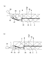
- FIG. 1A and 1B are diagrams showing a method and an apparatus for forming a display light beam 2 in a holographic manner, wherein FIG. 1A is a diagram showing a normal optical system for observing a virtual image, and FIG. It is a figure which shows a system
- FIG. 1A and 1B are diagrams illustrating a display device according to a first embodiment, in which FIG. 1A illustrates a case where a divergent light beam is incident on a transparent substrate, and FIG. 2B illustrates a case where a parallel light beam is incident on a transparent substrate.
- FIG. 1A illustrates a case where a divergent light beam is incident on a transparent substrate
- FIG. 2B illustrates a case where a parallel light beam is incident on a transparent substrate.
- a display light beam is formed in a holographic manner, and this display light beam is repeatedly reflected on the inner surface of the transparent substrate and propagated, and each time the inner surface is reflected, a part of the display light beam is removed from the transparent substrate. Inject and display. As the display light beam is propagated, a plurality of display light beams are emitted from the transparent substrate. In this way, the display light beam is emitted from almost the entire surface of the transparent substrate.
- the display light beam is formed holographically. Therefore, a display method having high optical performance can be realized while being small and thin.
- forming the display light beam in a holographic manner means forming (reproducing) the display light beam using a hologram.
- a plurality of display light beams are emitted from a transparent substrate as the display light beam is propagated.
- the observer can see the image by looking at any one display light beam or by viewing a plurality of display light beams. That is, it can be considered that the display light beams are combined to form one thick display light beam.
- the display beams are considered to be combined into one thick display beam. be able to.
- a plurality of display light beams are emitted from the transparent substrate, which is equivalent to one thick display light beam being emitted from the entire surface of the transparent substrate. Therefore, the entire surface of the transparent substrate is the exit pupil, and the size of the transparent substrate is the size of the exit pupil. Therefore, since the pupil is large like a loupe which is itself a pupil, an observer can easily observe a virtual image without bringing his face close to the display device.
- the display light beam emitted from the transparent substrate is a light beam for displaying a virtual image at infinity. That is, when the observer looks at the display light beam, a virtual image is formed at infinity (far). Therefore, for each of the plurality of display light beams emitted from the transparent substrate, a virtual image is formed at infinity when the observer views these display light beams. As a result, even if the observer's eyes are presbyopia that focuses only on the near point, the observer can see a focused display. In addition, the observer can see a virtual image formed at infinity regardless of which display light beam is viewed or a plurality of display light beams are viewed simultaneously.
- This display light beam (display light beam formed in a holographic manner) is parallel light.
- the display light beam is reflected, the reflected display light beam is amplitude-divided, and the light beam traveling in the same direction as the traveling direction of the reflected display light beam is reflected by the amplitude division.
- the display light beam may be a light beam generated by diffraction.
- FIG. 1 is a diagram showing the basic configuration of the display device of this embodiment and how the display light beam propagates.
- FIG. 1A shows a divergent light beam incident on a transparent substrate
- FIG. 1B shows a parallel light beam. The case where it injects into the transparent board
- the display device of this embodiment includes LCOS (Liquid Crystal On Silicon) 3, 3 ′, a transparent substrate 4, and a diffraction grating 5.
- LCOS 3 and 3 ′ are SPMs (Spatial Phase Modulators), which are hologram display elements that form the display light beam 2 in a holographic manner. Note that a transmissive liquid crystal display element can be used in place of the LCOSs 3 and 3 '.
- the transparent substrate 4 has an interface (first transmission surface) 4a and an interface (second transmission surface) 4b.
- the display light beam 2 is reflected (total reflection) on the inner surface thereof, that is, the interface 4 a or the interface 4 b. As a result, the display light beam 2 propagates inside the transparent substrate 4.
- the diffraction grating 5 is a branching means. Each time the display light beam 2 undergoes internal reflection, the diffraction grating 5 emits a part of the light beam to the outside of the transparent substrate 4.
- the diffraction grating 5 is located between the interface 4a and the interface 4b.
- the diffraction grating 5 is disposed so as to face the LCOSs 3 and 3 '.
- the diffraction grating 5 may be composed of a volume hologram.
- FIG. 1A shows a case where illumination light from a light source (not shown) is a divergent light beam.
- the divergent light beam 1 enters from the interface 4a and enters the LCOS 3 provided at the interface 4b.
- a phase hologram hologram pattern or phase pattern
- LCOS 3 phase hologram
- the display light beam 2 is generated as the first-order diffracted light (first-order light) of the hologram displayed on the LCOS 3.
- the 0th-order diffracted light (0th-order light) specularly reflected by the LCOS 3 is emitted from the transparent substrate 4.
- the phase hologram displayed on the LCOS 3 is a hologram that generates a parallel display light beam 2 when the divergent light beam 1 is incident.
- the display light beam 2 corresponds to an on-axis display light beam (light beam emitted from the center of the image).
- the off-axis display light beam (light beam emitted from other than the center of the image) is generated holographically from the LCOS 3, the off-axis display light beam is not shown.
- FIG. 1B shows a case where the illumination light from the light source (not shown) is a parallel light flux.
- the parallel light beam 1 ' enters from the interface 4a and enters the LCOS 3' provided at the interface 4b.
- LCOS 3 ' a phase hologram (hologram pattern or phase pattern) is displayed. Therefore, the illumination light incident on the LCOS 3 'is diffracted by the phase hologram (LCOS 3').
- the display light beam 2 is generated holographically from the LCOS 3 '.
- the display light beam 2 is generated as the first-order diffracted light (first-order light) of the hologram displayed on the LCOS 3 '.
- the 0th-order diffracted light (0th-order light) specularly reflected by the LCOS 3 ′ exits the transparent substrate 4.
- the phase hologram displayed on the LCOS 3 ' is a hologram that generates a parallel display light beam 2 when the parallel light beam 1' is incident.
- the display light beam 2 corresponds to an on-axis display light beam (light beam emitted from the center of the image).
- An off-axis display light beam (light beam emitted from other than the center of the image) is also generated holographically from the LCOS 3 ', but the off-axis display light beam is not shown.
- a convergent light beam may be incident on the LCOSs 3 and 3 '.
- a hologram that generates a parallel display light beam when the converged light beam is incident may be displayed on the LCOS 3, 3'.
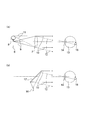
- FIG. 2A is a diagram showing a normal optical system when observing a virtual image
- FIG. 2B is a diagram showing an optical system that forms a display light beam in a holographic manner.
- This display light beam is a light beam when the virtual image is observed (parallel light beams 10 and 12 in FIG. 2A).
- the optical system shown in FIG. 2A is composed of a display element 6 such as an LCD and a lens 7.
- a display element 6 such as an LCD
- a lens 7 When the display element 6 is placed at the focal position (front focal position) of the lens 7, the image 8 displayed on the display element 6 is projected at infinity by the lens 7.
- a solid line 9 is a light beam emitted from the center (on the axis) of the display element 6, and a broken line 11 is a light beam emitted from the end (off-axis) of the display element.
- the light beam indicated by the solid line 9 becomes a parallel light beam 10 and exits the lens 7. Further, the light beam indicated by the broken line 11 also becomes a parallel light beam 12 and exits the lens 7.
- the parallel light beams 10 and 12 enter the pupil 14 of the observer's eye 13. Thereby, the observer can see the image 15 of the image 8. Since the luminous fluxes 10 and 12 incident on the observer's pupil 14 are parallel luminous fluxes, the observer views a virtual image at the back of the display device (left side of the display element 6 in FIG. 2A), that is, at infinity. You are observing. Therefore, even if the observer's eyes are presbyopia whose focus is only at the near point, the observer can see the focused image 8.
- FIG. 2 (b) shows an optical system when the parallel light beams 10 and 12 are formed in a holographic manner.
- This optical system includes a coherent light source 16 and an SPM (spatial phase modulation element) 17.
- As the coherent light source 16 there is an LD (laser diode).
- the SPM 17 includes the LCOS described above.
- the SPM 17 is a hologram display element. In the future, the hologram display element will be referred to as SPM.
- the hologram has a hologram pattern.
- the hologram pattern is an interference pattern formed by two wavefronts.
- One wavefront is a wavefront emitted from the lens 7 in FIG. 2A
- the other wavefront is a wavefront emitted from the coherent light source 16 in FIG.
- the wavefronts (parallel light beams 10 and 12) emitted from the lens 7 include image information of the image 8.
- the wavefront emitted from the coherent light source 16 is a wavefront that generates interference fringes and at the same time is a wavefront that generates reproduction light from a hologram.
- the light emitted from the display element 6 is incoherent light. Therefore, even if the light emitted from the display element 6 and the wavefront emitted from the coherent light source 16 are overlapped, there is no interference. That is, a hologram pattern cannot be obtained. Therefore, in practice, a hologram (hologram pattern) is obtained by calculation. The calculated hologram is displayed on the SPM 17 and illuminated by the coherent light source 16. By doing so, holograms, that is, parallel light beams 10 and 12 are reproduced. The parallel light beam 10 out of the parallel light beams 10 and 12 is the display light beam 2 shown in FIG.
- the observer can observe the image 8 when the observer sees the parallel light beams 10 and 12 formed in the holographic manner. That is, the parallel light beams 10 and 12 are incident on the pupil 14 of the observer's eye 13 to form an image 15.
- the lens 7 needs to project an off-axis image (an image displayed on the periphery of the display element 6) onto the eye 13 with high resolution.
- the lens 7 is actually composed of a plurality of lenses.
- the diameter of the lens 7 needs to be increased. For this reason, when the optical system shown in FIG. 2A is used for the display device, it is difficult to reduce the thickness and size of the display device.
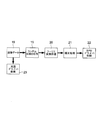
- FIG. 3 is a block diagram showing a process for obtaining a hologram by calculation.
- image data 18 is prepared.
- the image data 18 is data input to the display element 6 in FIG.
- the wavefront emitted from the lens 7 is obtained by Fourier transforming the image data 18 in the Fourier transform process 20.
- the spatial intensity distribution obtained by Fourier transform also causes a spatial intensity distribution at the same time as the spatial frequency distribution, a phase hologram with good diffraction efficiency cannot be formed. Therefore, a random phase is applied 19 before the Fourier transform process 20. If random phase information is given (superimposed) to the image data 18 in advance, the value of the spatial intensity after Fourier transform can be averaged over the entire spatial frequency plane, that is, the spatial intensity can be made substantially equal. As a result, the hologram can be a phase hologram having only phase information.
- This correction process 21 is a correction process based on the arrangement of the optical system.
- the hologram parallel light beams 10 and 12
- the correction process 21 calculates a hologram based on this spherical wave information. Thereafter, the calculation result (hologram information) is input to the SPM driver control 22. Then, a hologram is displayed on the SPM 17 (LCOS3, 3 'in FIG. 1) according to control information from the SPM driver control 22.
- the diffraction efficiency of the SPM 17 is almost constant, so that both bright scene images and dark scene images have the same brightness. Therefore, when the display light beam is formed holographically, it is necessary to control the amount of light incident on the SPM 17 according to the total amount of light of the image. Therefore, the brightness of the light source is controlled by inputting the total light amount data of the image data 18 to the light source driver 23.
- the display light beam 2 emitted from the LCOS 3 is totally reflected by the interface 4 a of the transparent substrate 4 and enters the diffraction grating 5.
- the diffraction grating 5 a part of the display light beam 2 is diffracted.
- the diffraction direction is the normal direction of the interface 4a.
- the light beam diffracted by the diffraction grating 5 exits from the transparent substrate 4 to become a display light beam 2a.
- the display light beam 2 transmitted through the diffraction grating 5 is further totally reflected by the interface 4 b of the transparent substrate 4 and passes through the diffraction grating 5.
- the display light beam 2 transmitted through the diffraction grating 5 is totally reflected again by the interface 4 a and enters the diffraction grating 5.
- a part of the display light beam 2 is diffracted.
- the diffraction direction is the normal direction of the interface 4a.
- the light beam diffracted by the diffraction grating 5 exits from the transparent substrate 4 to become a display light beam 2b.
- the display light beam 2 propagates through the transparent substrate 4 to form a new display light beam 2c.
- a large number of display light beams (2a, 2b, 2c) are emitted from the entire surface of the transparent substrate 4 (interface 4a).
- the observer can observe a virtual image by causing at least one of the display light beams 2a, 2b, and 2c to enter the eye.
- the observer can observe the moving image. If the image data is a still image, the observer can observe the still image.
- the display light beam 2 is formed using LCOS3. Therefore, a display device having high optical performance can be realized while being small and thin. Further, the light beam incident on the LCOS 3 may be only the axial light beam. For this reason, the light emitted from the light source can be used as a light beam incident on the LCOS 3 as it is. In this case, since a lens for light beam conversion is not required, the display device can be reduced in thickness and size.
- the display device can be reduced in thickness and size.
- the display light beam 2 is formed holographically by LCOS 3 and 3 ′. Therefore, as described above, the display device can be reduced in thickness and size.
- a plurality of display light beams 2a, 2b, and 2c are emitted from the transparent substrate 4 as the display light beam is propagated.
- the observer can observe a virtual image by causing at least one display light beam to enter the pupil of the eye.
- the display beam includes an on-axis beam that displays the center of the image and an off-axis beam that displays the edge of the image.
- Each display beam is thick, and the exit pupil is the entire surface of the transparent substrate from which the display beam is emitted. It becomes. Therefore, the permissible range of eye alignment with respect to the display light beam (transparent substrate 4) is wider than when the diameter of the display light beam is small (thin). As a result, the observer can easily observe the virtual image.
- LCOS or a transmissive liquid crystal display element is used for SPM, but a deformable mirror can also be used.
- deformable mirrors there are a type that deflects each of a plurality of micromirrors and a type that deforms one thin mirror.
- the display device can be manufactured as follows, for example. First, a concave portion is formed in a part of the transparent substrate 4, that is, a portion where the diffraction grating 5 is provided. And the diffraction grating 5 is arrange
- FIG. 4A shows a case where a divergent light beam is incident on a transparent substrate
- FIG. 4B shows a case where a parallel light beam is incident on a transparent substrate.
- LCOS reflection type liquid crystal display element
- SPM spatial phase modulation element
- the display device of the present embodiment includes a light source 24, LCOS (reflection type liquid crystal display elements) 3, 3 ', a transparent substrate 4, and a diffraction grating 5.
- LCOS reflection type liquid crystal display elements
- the transparent substrate 4 has an interface (first transmission surface) 4a and an interface (second transmission surface) 4b.
- the display light beam 2 is reflected (total reflection) on the inner surface thereof, that is, the interface 4 a or the interface 4 b. As a result, the display light beam 2 propagates inside the transparent substrate 4.
- LCOS 3 and 3 ′ are SPMs (spatial phase modulation elements), which are elements that form the display light beam 2.
- the diffraction grating 5 is a branching means. Each time the display light beam 2 undergoes internal reflection, the diffraction grating 5 emits a part of the light beam to the outside of the transparent substrate 4.
- the diffraction grating 5 is located between the interface 4a and the interface 4b.
- the diffraction grating 5 is disposed so as to face the LCOSs 3 and 3 '.
- the diffraction grating 5 may be constituted by a volume hologram. Further, when the transparent substrate 4 is viewed from the light source 24 side, the LCOSs 3 and 3 ′ and the diffraction grating 5 are arranged adjacent to each other.
- the display light beam 2 is emitted from the LCOSs 3 and 3 '. As described with reference to FIG. 1, the display light beam 2 propagates through the transparent substrate 4, and the display light beams 2 a, 2 b, and 2 c are emitted outside the transparent substrate 4. In the display device shown in FIG. 4B, the display light beams 2b and 2c are generated but are not shown.
- the LCOS 3 shown in FIG. 4A displays a hologram (phase hologram) in which a parallel display light beam 2 is generated when the divergent light beam 1 is incident. Therefore, the divergent light beam 1 emitted from the light source 24 can be directly incident on the LCOS 3 without conversion. As a result, the light source 24 can be brought close to the transparent substrate 4 or the LCOS 3. In FIG. 4A, the light source 24 is in contact with the interface 4a. Therefore, the display device can be reduced in thickness and size.
- a hologram phase hologram
- the light source 24 may be positioned closer to the interface 4b than the interface 4a.
- a recess hole may be formed from the interface 4a toward the inside of the transparent substrate 4, and the light source 24 may be disposed in the recess.
- the display device can be further reduced in thickness and size.
- the light source 24 may be disposed at a position slightly distant from the interface 4a (in the vicinity of the interface 4a) as long as it does not interfere with the reduction in thickness and size.
- the display device shown in FIG. 4A does not require a lens for light beam conversion, so that the display device can be reduced in thickness and size.
- the LCOS 3 ′ shown in FIG. 4B displays a hologram in which a parallel display light beam 2 is generated when the parallel light beam 1 ′ is incident. Therefore, the lens 25 is disposed in the optical path from the light source 24 to the LCOS 3 ′. The lens 25 converts the divergent light beam 1 into a parallel light beam 1 '.
- the display device shown in FIG. 4B since the lens 25 exists, it is difficult to arrange the light source 24 in the vicinity of the interface 4a. Therefore, it cannot be said that the display device is reduced in thickness and size as compared with the display device illustrated in FIG.
- the lens 25 can be simplified, for example, the number of lenses constituting the lens 25 can be reduced.
- a single lens is sufficient for the lens 25.
- the lens aberration may be corrected in the above-described correction process 21 (FIG. 3). Therefore, even when the light beam incident on the LCOS 3 ′ is a parallel light beam, the display device can be made thinner and smaller than the conventional display device (FIG. 2A).
- the LCOSs 3 and 3 ' may be arranged on the interface a side (between the interface a and the interface b) with respect to the interface b.
- the hologram information is corrected by the correction processing 21 (FIG. 3). By doing in this way, when the divergent light beam 1 is incident on the LCOS 3, an accurate display light beam 2 is formed.
- the hologram information displayed in the LCOS 3 ′ is corrected in the hologram information in the correction process 21 (FIG. 3). By doing so, an accurate display light beam 2 is formed when the parallel light beam 1 ′ is incident on the LCOS 3 ′.
- the 0th-order light (0th-order diffracted light) reflected by the LCOS 3 is emitted from the transparent substrate 4 while diverging, so that the display (observation of a virtual image) is adversely affected. There is nothing.
- the zero-order light reflected by the LCOS 3 ′ is emitted from the transparent substrate 4 as it is (in the state of a parallel light beam) as it is, which adversely affects the display (observation of a virtual image). Will not affect.
- the 0th-order light passes through the transparent substrate 4 and the primary light (display light beam 2) satisfies the condition of total reflection on the transparent substrate 4 (interfaces 4a and 4b). , LCOS3 and LCOS3 ′ are arranged. Therefore, the 0th order light does not adversely affect the display (observation of a virtual image).
- the light beam incident on the observer's pupil is a parallel light beam, so the observer observes a virtual image at the back of the display device, that is, at infinity. Therefore, even if the observer's eyes are presbyopia whose focus is only at the near point, the observer can see the focused image 8.
- the display device of the second embodiment is shown in FIG.
- the display device of the present embodiment has another LCOS 26 in the optical path from the light source 24 to the LCOS 3 ′.
- the LCOS 3 ' is arranged on the interface 4a side
- the LCOS 26 is arranged on the interface 4b side.
- the member which produces the same function as the display apparatus of 1st Embodiment attaches
- LCOS 3 displays a hologram that generates parallel display light beam 2 when parallel light beam 1' is incident.
- the LCOS 26 displays a hologram that generates a parallel light beam 1 'when the divergent light beam 1 is incident.
- the divergent light beam 1 emitted from the light source 24 enters the LCOS 26.
- the divergent light beam 1 is converted into a parallel light beam 1 ′ by the LCOS 26.
- the converted parallel light beam 1 ′ is emitted from the LCOS 26.
- the parallel light beam 1 ′ emitted from the LCOS 26 is incident on the LCOS 3 ′.
- the display light beam 2 is generated (reproduced) from the parallel light beam 1 ′, and the display light beam 2 is emitted from the LCOS 3 ′.
- the display light beam 2 propagates through the transparent substrate 4, and the display light beam 2 a (2 b, 2 c) is emitted outside the transparent substrate 4.
- the lens 25 must be disposed between the light source 24 and the interface 4a. Therefore, the light source 24 is arranged at a position away from the interface 4a. As a result, the display device cannot be sufficiently reduced in thickness and size.
- the LCOS 26 serving as the lens 25 can be arranged on the interface 4b side. Therefore, the light source 24 can be brought close to the interface 4a. As a result, the display device can be reduced in thickness and size to the same extent as the display device (first embodiment) shown in FIG.
- the LCOS 3 ′ and the diffraction grating 5 are arranged so as to overlap when the transparent substrate 4 is viewed from the light source 24 side. However, the LCOS 3 ′ and the diffraction grating 5 are actually arranged adjacent to each other so that the display light beam 2 a diffracted by the diffraction grating 5 does not pass through the LCOS 3 ′.
- the LCOS 26 can be replaced with a normal hologram (hologram lens). In this case, a volume hologram is preferable in terms of diffraction efficiency.
- FIG. 6 shows a display device according to the third embodiment.
- 6A shows a case where a divergent light beam is incident on a transparent substrate
- FIG. 6B shows a case where a parallel light beam is incident on a transparent substrate.
- an LCD transmission type liquid crystal display element
- SPM spatial phase modulation element
- the display device of this embodiment includes a light source 24, LCDs (transmission type liquid crystal display elements) 27 and 27 ', a transparent substrate 4, and a diffraction grating 5.
- the member which produces the same function as the display apparatus of 1st Embodiment attaches
- LCDs 27 and 27 ′ are SPMs (spatial phase modulation elements) and are elements that form the display light beam 2.
- the divergent light beam 1 from the light source 24 is incident on the LCD 27.
- the parallel light beam 1 'from the light source 24 is incident on the LCD 27'.
- the display light beam 2 is formed as the first-order diffracted light (primary light).
- the action of the display light beam 2 propagating through the transparent substrate 4 and the display light beams 2a, 2b, 2c exiting the transparent substrate 4 is the same as that of the display device of the first embodiment.
- the LCD 27 shown in FIG. 6A displays a hologram (phase hologram) that generates a parallel display light beam 2 when the diverging light beam 1 is incident. Therefore, the divergent light beam 1 emitted from the light source 24 can be directly incident on the LCD 27 without being converted. As a result, the light source 24 can be brought close to the transparent substrate 4 or the LCD 27. Therefore, the display device can be reduced in thickness and size.
- a hologram phase hologram
- the LCD 27 ′ shown in FIG. 4B displays a hologram that generates a parallel display light beam 2 when the parallel light beam 1 ′ is incident. Therefore, it is necessary to arrange a lens (not shown) in the optical path from the light source 24 to the LCD 27 '. However, only the axial light beam needs to enter the LCD 27 '. Therefore, the lens can be simplified, for example, the number of lenses constituting the lens can be reduced. In the display device shown in FIG. 4B, a single lens is sufficient. Further, the lens aberration may be corrected in the above-described correction process 21 (FIG. 3). Therefore, even when the light beam incident on the LCD 27 ′ is a parallel light beam, the display device can be made thinner and smaller than the conventional display device (FIG. 2A).
- the LCDs 27 and 27 ' may be disposed at a position slightly away from the interface b as long as the thickness and size are not affected.
- the LCDs 27 and 27 ′ may be arranged on the interface a side (between the interface a and the interface b) with respect to the interface b.
- the light source 24 and the LCDs 27 and 27 ' may be arranged on the interface a side.
- the hologram information displayed on the LCD 27 is subjected to hologram information correction processing in correction processing 21 (FIG. 3). By doing so, when the divergent light beam 1 enters the LCD 27, an accurate display light beam 2 is formed. Similarly, the hologram information displayed on the LCD 27 ′ is corrected in the hologram information in the correction process 21 (FIG. 3). By doing so, an accurate display light beam is formed when the parallel light beam 1 'is incident.
- the 0th-order light (0th-order diffracted light) transmitted through the LCD 27 is emitted from the transparent substrate 4 while diverging, so that the display (observation of a virtual image) is adversely affected. There is nothing.
- the 0th-order light 28 transmitted through the LCD 27 ′ is emitted from the vertically transparent substrate 4 as it is (in the state of a parallel light beam), so that it is displayed (observation of a virtual image). Will not be adversely affected.
- the 0th-order light passes through the transparent substrate 4 and the primary light (display light beam 2) satisfies the condition of total reflection on the transparent substrate 4 (interfaces 4a and 4b).
- LCD 27 and LCD 27 ' are arranged. Therefore, the 0th order light does not adversely affect the display (observation of a virtual image).
- the light beam incident on the observer's pupil is a parallel light beam, so the observer observes a virtual image at the back of the display device, that is, at infinity. Therefore, even if the observer's eyes are presbyopia whose focus is only at the near point, the observer can see the focused image 8.
- LCD which displays normal intensity
- it is not a phase hologram but an amplitude hologram that is displayed on the LCD, the diffraction efficiency is lowered.
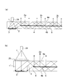
- FIGS. 7A is a diagram illustrating the configuration of the first transparent substrate and the state of propagation of the display light beam
- FIG. 7B is a diagram illustrating the configuration of the second transparent substrate and the state of propagation of the display light beam. is there.
- FIG. 8 is a diagram showing the overall configuration of the display device.
- the display device of this embodiment includes a first transparent substrate 30 and a second transparent substrate 36, as shown in FIG.
- the first transparent substrate 30 is located at the end of the second transparent substrate 36, and the first transparent substrate 30 is fixed to the second transparent substrate 36 at this position.
- the first transparent substrate 30 includes an SPM 29, a beam splitter 31, and a diffraction grating 32, as shown in FIG.
- the second transparent substrate 36 includes a beam splitter 37, a diffraction grating 38, and a diffraction grating 39, as shown in FIG. 7B.
- the diffraction grating 32, the diffraction grating 38, and the diffraction grating 39 are preferably volume holograms.
- the SPM 29 is a spatial phase modulation element that forms the display light beam 34 in a holographic manner. Further, on the first transparent substrate 30 and the second transparent substrate 36, the display light beam 34 is repeatedly reflected from the inner surface and propagated. Further, the beam splitter 31 causes a part of the display light beam 34 to be incident on the second transparent substrate 36 every time the display light beam 34 is internally reflected by the first transparent substrate 30. The beam splitter 37 causes a part of the display light beam 34 to be emitted from the second transparent substrate 36 every time the display light beam 34 is internally reflected by the second transparent substrate 36.
- the luminous flux (illumination light) and the display luminous flux incident on the display device show only the central ray of the axial luminous flux.
- a light beam it will be referred to as a light beam.
- the off-axis light beam is not clearly shown, it goes without saying that the off-axis light beam exists.
- the first transparent substrate 30 is made of a transparent member having a rectangular outer shape.
- An SPM 29, a beam splitter 31, and a diffraction grating 32 are arranged along the long side direction (X-axis direction).
- the display light beam 34 propagates along the long side direction.
- the thickness of the first transparent substrate 30 is 2 to 4 mm, for example.
- the outer shapes of the beam splitter 31 and the diffraction grating 32 are both rectangular. Further, the beam splitter 31 and the diffraction grating 32 are arranged to face each other. The beam splitter 31 is disposed between the two interfaces of the first transparent substrate 30. The diffraction grating 32 is disposed on one interface side of the first transparent substrate 30.
- a notch is formed at the end of this one interface.
- SPM29 is arrange
- one of the end surfaces (short side) sandwiched between the two interfaces is an inclined surface. From this inclined surface, a parallel light beam 33 enters.
- a parallel light beam 33 is incident on the SPM 29 from an LD light source (not shown).
- the display light beam 34 is formed as diffracted primary light by the hologram displayed on the SPM 29.
- the display light beam 34 is totally reflected on the inner surface (interface) of the first transparent substrate 30.
- the totally reflected display light beam 34 is separated into transmitted light and reflected light by the beam splitter 31.
- the transmitted light is incident on the diffraction grating 32 provided at the interface of the first transparent substrate 30. Then, it is diffracted by the diffraction grating 32 toward the beam splitter 31 side. The diffracted light becomes a display light beam 34a and exits the first transparent substrate 30 vertically.
- the display light beam 34a vertically emitted from the first transparent substrate 30 is incident on the second transparent substrate 36 (FIG. 7B).
- the reflected light is again totally reflected by the inner surface (interface) of the first transparent substrate 30 and enters the beam splitter 31 again. Then, the light is again separated into transmitted light and reflected light by the beam splitter 31.
- the reflected light separated again is totally reflected again by the inner surface (interface) of the first transparent substrate 30.
- the display light beam 34c is generated by the same action as the display light beam 34a and the display light beam 34b.
- the display light beam 34 repeats total reflection on the inner surface (interface) of the first transparent substrate 30 and propagates in the first transparent substrate 30. Then, while propagating, the display light beams 34 a, 34 b, 34 c are emitted vertically from the first transparent substrate 30 and incident on the second transparent substrate 36.
- the display light beams 34 a, 34 b, 34 c are emitted vertically from the first transparent substrate 30 and incident on the second transparent substrate 36.
- three display light beams to be emitted are shown (34a, 34b, 34c). The number of light beams is not limited to this.
- the diffraction grating 32 is preferably a volume hologram with high diffraction efficiency.
- the 0th-order light 35 specularly reflected by the SPM 29 is not totally reflected by the first transparent substrate 30 and is directly emitted to the outside of the first transparent substrate 30.
- the emitted zero-order light 35 is extinguished by a trap mechanism (not shown).
- the second transparent substrate 36 is made of a transparent member having a substantially rectangular outer shape.
- the length in the X-axis direction (short side) is the same as the length of the long side of the first transparent substrate 30.
- the length in the Z-axis direction (long side) is longer than the length of the short side of the first transparent substrate 30.
- the outer shape of the second transparent substrate 36 is not limited to a rectangle.
- the display light beam 34 propagates along the Z-axis direction. Note that the thickness of the second transparent substrate 36 is, for example, 2 to 4 mm.
- the outer shape of the diffraction grating 39 is rectangular like the diffraction grating 32. It is preferable that the length of the short side of the diffraction grating 39 does not exceed the length of the short side of the first transparent substrate 30.
- the diffraction grating 39 is disposed on one interface side of the second transparent substrate 36. Further, the diffraction grating 39 is disposed at a position facing the diffraction grating 32.
- Each of the beam splitter 37 and the diffraction grating 38 is provided in a range that does not overlap with the diffraction grating 39 (the first transparent substrate 30). Further, the beam splitter 37 and the diffraction grating 38 are arranged so as to face each other. The beam splitter 37 is disposed between the two interfaces of the second transparent substrate 36. The diffraction grating 38 is disposed on one interface of the second transparent substrate 36 (interface on which the diffraction grating 39 is disposed).
- the display light beams 34 a, 34 b, 34 c incident on the second transparent substrate 36 are diffracted by the diffraction grating 38.
- the diffracted display light beams 34 a, 34 b and 34 c are totally reflected by the inner surface (interface) of the second transparent substrate 36 and enter the beam splitter 37. From here on, explanation will be made using the display light beam 34a.
- the display light beam 34 a is separated into transmitted light and reflected light by a beam splitter 37.
- the transmitted light is incident on the diffraction grating 38. Then, it is diffracted by the diffraction grating 38 toward the beam splitter 37 side.
- the diffracted light becomes a display light beam 34d, and exits the second transparent substrate 36 vertically.
- the reflected light is totally reflected again by the inner surface (interface) of the second transparent substrate 36 and enters the beam splitter 37 again. Then, the light is again separated into transmitted light and reflected light by the beam splitter 37.
- the reflected light separated again is totally reflected again by the inner surface (interface) of the second transparent substrate 36.
- the display light beam 34f is generated by the same action as the display light beam 34d and the display light beam 34e.
- the display light beam 34a repeats total reflection on the inner surface (interface) of the second transparent substrate 36 and propagates through the second transparent substrate 36. Then, the display light beams 34d, 34e, and 34f are emitted vertically from the second transparent substrate 36 one after another while propagating. The same applies to the display light beams 34b and 34c. That is, as shown in FIG. 8, the display light beam 34 spreads in one direction 41 of the display device while propagating through the inside of the first transparent substrate 30 and is propagated through the inside of the second transparent substrate 36. It spreads in the other direction 42 of the display device. As a result, the display light beam 43 is emitted from the entire surface 40 of the display device.
- the SPM 29 displays a hologram that generates the parallel display light beam 34 when the parallel light beam 33 is incident. Therefore, it is necessary to arrange a lens (not shown) in the optical path from the light source to the SPM 29. However, only the axial light beam needs to enter the SPM 29. Therefore, the lens can be simplified, for example, the number of lenses constituting the lens can be reduced. In the display device of this embodiment, a single lens is sufficient as the lens. Further, the lens aberration may be corrected in the above-described correction process 21 (FIG. 3). Therefore, even when the light beam incident on the SPM 29 is a parallel light beam, the display device can be made thinner and smaller than the conventional display device (FIG. 2A).
- a divergent light beam may be incident on the SPM 29. Then, a hologram in which a parallel display light beam 34 is generated when a divergent light beam is incident on the SPM 29 may be displayed. In this way, the divergent light beam emitted from the light source can be directly incident on the SPM 29 without conversion. As a result, the light source can be brought closer to the transparent substrate 30 and the SPM 29. As a result, the display device can be reduced in thickness and size. Instead of the divergent light beam, a convergent light beam may be incident on the SPM 29.
- a plurality of display light beams 34d, 34e, and 34f are emitted from the second transparent substrate 36.
- the observer can see the image by looking at any one display light beam or by viewing a plurality of display light beams. That is, it can be considered that the display light beams are combined to form one thick display light beam.
- the display beams are considered to be combined into one thick display beam. be able to.
- a plurality of display light beams are emitted from the surface 40 of the display device.
- the entire surface 40 of the display device is the exit pupil
- the size of the surface 40 of the display device is the size of the exit pupil. Therefore, since the pupil is large like a loupe which is itself a pupil, an observer can easily observe a virtual image without bringing his face close to the display device.
- the display light beams 34d, 34e, and 34f (display light beam 43) emitted from the second transparent substrate 36 are light beams that display a virtual image at infinity. That is, when the observer looks at the display light beam, a virtual image is formed at infinity (far). Therefore, for each of the plurality of display light beams emitted from the second transparent substrate 36, a virtual image is formed at infinity when the observer views these display light beams. As a result, even if the observer's eyes are presbyopia that focuses only on the near point, the observer can see a focused display.
- a display device having a two-dimensional expansion can be obtained by using two transparent substrates.
- the surface on which the SPM 29 is arranged is inclined with respect to the surface on which the diffraction grating 32 is provided (FIG. 7A).
- Such a configuration is effective when the diffraction angle of the display light beam 34 emitted from the SPM 29 cannot be sufficiently large.
- this diffraction angle can be made sufficiently large, it is not necessary to incline the surface on which the SPM 29 is disposed with respect to the surface on which the diffraction grating 32 is provided. What is necessary is just to carry out similarly to the display apparatus of 1st-3rd embodiment.
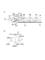
- FIG. 9A is a diagram illustrating a configuration of a first transparent substrate
- FIG. 9B is a diagram illustrating a relationship between incident light, diffracted light, and zeroth-order light.
- a hologram is displayed on the SPM (LCOS, LCD) 44.
- a hologram is a kind of diffraction grating. Therefore, as shown in FIG. 9B, the incident light (incident angle ⁇ R ) incident on the SPM 44 is diffracted at the diffraction angle ⁇ S. As a result, diffracted light is emitted from the SPM 44.
- the SPM 44 also emits zero-order light. This zero-order light is reflected by S at a reflection angle ⁇ R. Inject from PM44.
- the relationship between the incident angle ⁇ R , the diffraction angle ⁇ S and the pitch d of the diffraction grating is as follows. Note that ⁇ is the wavelength of incident light.
- the SPM 44 has a structure in which fine pixels are arranged one-dimensionally or two-dimensionally. A hologram is displayed using these fine pixels. Therefore, the size of two fine pixels, that is, twice the pixel pitch corresponds to the pitch d of the diffraction grating.
- the diffraction angle ⁇ S decreases as the pitch d of the diffraction grating increases, that is, as the pixel pitch of the SPM 44 increases.
- the reflection angle ⁇ R is constant, if the diffraction angle ⁇ S becomes small, it becomes difficult to separate the reflected light and the diffracted light.
- the surface on which the SPM 44 is arranged is inclined with respect to the surface on which the diffraction grating 32 is provided. In this way, it becomes easy to separate reflected light and diffracted light.
- the angle of view of the display device is ensured ⁇ 5.7 degrees.
- An angle of view of ⁇ 5.7 degrees is assumed when the display of a mobile device such as a mobile phone is viewed at a clear viewing distance. Since the field angle range is 11.4 degrees, the display light beam 34L (the off-axis principal ray of the display light beam (diffracted light or first-order diffracted light)) and the 0th order are separated in order to separate the display light beam 34 and the 0th order light 35.
- the angle difference with light needs to be at least 12 degrees.
- the angle formed between the display light beam 34 (the off-axis principal ray of the display light beam 34L) and the zero-order light 35 is 0.6 degrees, and the zero-order light 35 can be separated.
- the pixel pitch of the SPM 44 that displays the phase information is 3 ⁇ m. Then, the pitch of the diffraction grating (one state of the hologram) displayed on the SPM 44 is 6 ⁇ m.
- the incident angle ⁇ R is 60 degrees
- the diffraction angle ⁇ S is 72 degrees according to Equation 1. The required angle difference of 12 degrees can be secured.
- the display light beam 34 is incident on the inner surface (interface) of the transparent substrate 30 at an incident angle of 51.6 degrees and passes through the transparent substrate 30 with total reflection. Can propagate.
- FIG. 10 shows a display device of the fifth embodiment.
- (A) shows a case where the spatial phase modulation element is a reflection type
- (b) shows a case where the spatial phase modulation element is a transmission type.
- the display device of the present embodiment captures zero-order light emitted from the spatial phase modulation element.
- the member which produces the same function as the display apparatus of 1st Embodiment attaches
- the propagation of the display light beam 2 and the emission from the transparent substrate 4 are the same as those of the display device of the first embodiment.
- the divergent light beam 1 emitted from the light source 24 is converted into a convergent light beam 46 by the lens 45 and is incident on the LCOS 47.
- the display light beam 2 is formed by the phase hologram displayed on the LCOS 47.
- an inclined surface is formed at the end of the interface 4a. This inclined surface is inclined toward the interface 4b.
- a lens 45 is disposed on the inclined surface.
- An inclined surface is also formed at the end on the interface 4b side. This inclined surface is inclined toward the interface 4a.
- the LCOS 47 is disposed on this inclined surface.
- a trap 48 is provided at a position where an inclined surface is formed from the interface 4b.
- the trap 48 is formed vertically from the interface 4 b toward the diffraction grating 5.
- the display device shown in FIG. 10B is an example in which the divergent light beam 1 emitted from the light source 24 is converted into a convergent light beam 46 by the lens 45 and is incident on the LCD 47 '.
- the display light beam 2 is formed by the phase hologram displayed on the LCD 47 '.
- the lens 45 is disposed on the side surface sandwiched between the interface 4a and the interface 4b. Further, the LCD 47 'is disposed obliquely between the interface 4a and the interface 4b. The LCD 47 ′ is disposed between the lens 45 and the trap 48.
- the light source 24 is, for example, a semiconductor laser.
- a divergent light beam 1 is emitted from the light source 24.
- the divergent light beam 1 is converted into a convergent light beam 46 by the lens 45.
- the convergent light beam enters the LCOS 47 and the LCD 47 '. From the LCOS 47 and the LCD 47 ′, zero-order light and a display light beam 2 are generated.
- the LCOS 47 is a reflective SPM. Therefore, the 0th-order light regularly reflected by the LCOS 47 is directed to the trap 48.
- the LCD 47 ' is a transmissive SPM. Therefore, the 0th-order light that travels straight (transmits) through the LCD 47 ′ travels toward the trap 48.
- the trap 48 is a member that absorbs or blocks light. Therefore, the zero-order light incident on the trap 48 is absorbed or blocked by the trap 48. As a result, the zero-order light does not adversely affect the display light beam 2 (observation of a virtual image).
- the convergent light beam 46 is incident on the LCOS 47 or the LCD 47 '.
- the 0th order light emitted from the LCOS 47 and the LCD 47 ' is also a convergent light beam. Therefore, the 0th order light does not spread before entering the trap 48. As a result, the zero-order light does not adversely affect the display light flux 2.
- the beam diameter of the zero-order light at the position of the trap 48 is preferably smaller than the area of the trap 48, and if possible, it should be condensed in a dot shape.
- the lens 45 may be integrated with the transparent substrate 4.
- LCOS or a normal hologram may be used in place of the lens 45 in the same manner as in the display device of the second embodiment. In this way, the display device can be reduced in thickness and size.
- the LCD 47 ′ is integrally disposed in the transparent substrate 4. However, actually, for example, the LCD 47 ′ is sandwiched between two transparent members.
- the LCD 47 may be replaced with the LCD 47 ', and the LCD 47' may be covered with another transparent member from the LCD 47 'side.
- FIG. 11 is a diagram illustrating light beams emitted from the display device according to the present embodiment, and is a diagram illustrating optical distances of the respective light beams.
- a display device according to the fourth embodiment will be described as an example.
- a display light beam 43 is emitted from the surface 40 of the second transparent substrate 36 of the display device.
- the display light beam 43 is composed of display light beams 34d, 34e, and 34f (in practice, however, in addition to the three light beams, many light beams are emitted from the surface 40. Ejecting).
- a part of the display light beam enters the pupil 51 of the observer's eye, so that the observer can see the display (virtual image).
- FIG. 11 shows a state in which the display light beam is emitted from the three positions 50a, 50b, and 50c.
- Each of the three display light beams is composed of a display light beam 34, a most off-axis display light beam 34Uo, and a most off-axis display light beam 34Lo.
- the display light beam 34 corresponds to the light beam emitted from the axis (the center of the image).
- the most out-of-axis display light beam 34Uo corresponds to the light beam emitted from the most off-axis (one end of the image).
- the most off-axis display light beam 34Lo corresponds to the light beam emitted from the most off-axis (the other end of the image).
- 50a, 50b, and 50c are optical positions of the SPM 29 (FIG. 8) when viewed from the observer side. This optical position is the distance from the surface 40 of the second transparent substrate 36 to the SPM 29.
- Reference numeral 50a denotes an optical position of the SPM 29 when the display light beam 34 is totally reflected once in the second transparent substrate 36 and emitted.
- Reference numeral 50b denotes an optical position of the SPM 29 when the display light beam is totally reflected twice in the second transparent substrate 36 and emitted.
- Reference numeral 50c denotes an optical position of the SPM 29 when the display light beam is totally reflected three times within the second transparent substrate 36 and emitted.
- the optical distance difference 49 is a distance propagated by one total reflection that occurs in the second transparent substrate 36. More specifically, it is the distance when the display light beam 34 reciprocates from the beam splitter 37 to the interface.
- optical positions of the SPM 29 are actually the same as the number of light beams that propagate by repeating total reflection in two dimensions.
- display light beams from the SPM 29 at a plurality of different optical positions are normally incident on the observer's pupil.
- the display light beam 34, the most off-axis display light beam 34Lo, and the most off-axis display light beam 34Uo are formed holographically by coherent light. Therefore, the display light beam 34, the most off-axis display light beam 34Lo, and the most off-axis display light beam 34Uo are also coherent light.
- the display light beam (34, 34L, 34U) from 50b is mainly incident on the pupil 51 of the observer, but the display light beam from 50a and 50c is also incident depending on the position of the pupil 51. To do.
- the display light beam from 50a, the display light beam from 50b, and the display light beam from 50c are each coherent light. For this reason, when the display light beam from 50b and the display light beam from 50a enter the observer's pupil 51, the two light beams interfere with each other, and the virtual image to be observed becomes an unintended image (virtual image). It is done.
- An unintended image is, for example, an image with degraded image quality.
- the coherence length of the light source 24 is preferably shorter than the difference 49 of the optical distance. That is, the coherence length of the light source 24 is preferably shorter than the distance propagated by one total reflection that occurs in the second transparent substrate 36. By doing so, it is possible to prevent an unintended image from being formed even when a plurality of display light beams having different optical distances enter the observer's eyes.
- SPM is used to generate a display light beam holographically.
- the display light beam can be generated holographically without using SPM.
- a hologram pattern may be recorded on the film, and this film may be disposed at the SPM position.
- the film may not be a film as long as it has a characteristic that the hologram pattern can be recorded only once.
- the display method and display device according to the present invention are useful in that they have high optical performance while being small and thin.
Abstract
Dans le procédé d'affichage, selon la présente invention, un flux lumineux d'affichage (2) se propage par réflexion interne répétée dans un substrat transparent (4) et, par émission d'une partie du flux lumineux d'affichage hors du substrat transparent (4) pour chaque réflexion interne dudit flux lumineux d'affichage, le flux lumineux d'affichage est émis à partir de sensiblement toute la surface du substrat transparent (4), le flux lumineux d'affichage étant formé de manière holographique. Le dispositif d'affichage selon la présente invention est pourvu d'un élément de modulation de phase spatiale (3) pour former un flux lumineux d'affichage, d'un substrat transparent (4) dans lequel le flux lumineux d'affichage se propage par réflexion interne répétée et d'un moyen de ramification (5) qui émet une partie du flux lumineux d'affichage (2) hors du substrat transparent (4) pour chaque réflexion interne du flux lumineux d'affichage.
Priority Applications (2)
| Application Number | Priority Date | Filing Date | Title |
|---|---|---|---|
| US14/638,234 US20150241844A1 (en) | 2012-09-05 | 2015-03-04 | Display Method and Display Apparatus |
| US15/936,010 US10534317B2 (en) | 2012-09-05 | 2018-03-26 | Display method and display apparatus |
Applications Claiming Priority (2)
| Application Number | Priority Date | Filing Date | Title |
|---|---|---|---|
| JP2012-194964 | 2012-09-05 | ||
| JP2012194964A JP5984591B2 (ja) | 2012-09-05 | 2012-09-05 | 表示方法及び表示装置 |
Related Child Applications (1)
| Application Number | Title | Priority Date | Filing Date |
|---|---|---|---|
| US14/638,234 Continuation US20150241844A1 (en) | 2012-09-05 | 2015-03-04 | Display Method and Display Apparatus |
Publications (1)
| Publication Number | Publication Date |
|---|---|
| WO2014038237A1 true WO2014038237A1 (fr) | 2014-03-13 |
Family
ID=50236862
Family Applications (1)
| Application Number | Title | Priority Date | Filing Date |
|---|---|---|---|
| PCT/JP2013/060911 WO2014038237A1 (fr) | 2012-09-05 | 2013-04-11 | Procédé et dispositif d'affichage |
Country Status (3)
| Country | Link |
|---|---|
| US (2) | US20150241844A1 (fr) |
| JP (1) | JP5984591B2 (fr) |
| WO (1) | WO2014038237A1 (fr) |
Families Citing this family (4)
| Publication number | Priority date | Publication date | Assignee | Title |
|---|---|---|---|---|
| JP2016085430A (ja) * | 2014-10-29 | 2016-05-19 | セイコーエプソン株式会社 | 虚像表示装置 |
| US10254542B2 (en) * | 2016-11-01 | 2019-04-09 | Microsoft Technology Licensing, Llc | Holographic projector for a waveguide display |
| JP7232182B2 (ja) | 2016-11-30 | 2023-03-02 | マジック リープ, インコーポレイテッド | 高分解能のデジタル化された表示のための方法及びシステム |
| IL308323A (en) | 2017-05-16 | 2024-01-01 | Magic Leap Inc | Systems and methods for mixed reality |
Citations (5)
| Publication number | Priority date | Publication date | Assignee | Title |
|---|---|---|---|---|
| JP2002520669A (ja) * | 1998-07-17 | 2002-07-09 | ブルックヘイブン サイエンス アソシエイツ | 小さな入口の光学パネル及び小さな入口の光学パネルの製造方法 |
| JP2007505353A (ja) * | 2003-09-10 | 2007-03-08 | ラマス リミテッド | 基板導光の光学装置 |
| JP2007240641A (ja) * | 2006-03-06 | 2007-09-20 | Harison Toshiba Lighting Corp | 面状発光デバイス |
| JP2008270222A (ja) * | 1997-01-13 | 2008-11-06 | Minnesota Mining & Manufacturing Co | 照明デバイス |
| JP2009516862A (ja) * | 2005-11-21 | 2009-04-23 | マイクロビジョン,インク. | 像誘導基板を有するディスプレイ |
Family Cites Families (14)
| Publication number | Priority date | Publication date | Assignee | Title |
|---|---|---|---|---|
| JPS465152Y1 (fr) | 1967-06-08 | 1971-02-23 | ||
| US6002829A (en) | 1992-03-23 | 1999-12-14 | Minnesota Mining And Manufacturing Company | Luminaire device |
| JP4605152B2 (ja) | 2004-03-12 | 2011-01-05 | 株式会社ニコン | 画像表示光学系及び画像表示装置 |
| JP4810949B2 (ja) * | 2005-09-29 | 2011-11-09 | ソニー株式会社 | 光学装置及び画像表示装置 |
| JP2007219106A (ja) * | 2006-02-16 | 2007-08-30 | Konica Minolta Holdings Inc | 光束径拡大光学素子、映像表示装置およびヘッドマウントディスプレイ |
| US8477315B2 (en) * | 2007-02-09 | 2013-07-02 | Seiko Epson Corporation | Volume hologram, light source device, illumination device, monitor, and image display device |
| JP2008216579A (ja) * | 2007-03-02 | 2008-09-18 | Olympus Corp | ホログラフィックプロジェクション方法及びホログラフィックプロジェクション装置 |
| JP4706737B2 (ja) * | 2008-08-18 | 2011-06-22 | ソニー株式会社 | 画像表示装置 |
| ES2758826T3 (es) * | 2008-09-16 | 2020-05-06 | Bae Systems Plc | Mejoras en o relativas a guías de ondas |
| WO2010149583A1 (fr) * | 2009-06-23 | 2010-12-29 | Seereal Technologies S.A. | Unité d'éclairage pour un écran d'affichage à vision directe |
| US11320571B2 (en) * | 2012-11-16 | 2022-05-03 | Rockwell Collins, Inc. | Transparent waveguide display providing upper and lower fields of view with uniform light extraction |
| EP2494388B1 (fr) * | 2009-10-27 | 2018-11-21 | DigiLens Inc. | Dispositif d'affichage de verre de lunettes holographique compact |
| WO2012062681A1 (fr) * | 2010-11-08 | 2012-05-18 | Seereal Technologies S.A. | Dispositif d'affichage, notamment visiocasque basé sur le multiplexage temporel et spatial de carreaux d'hologrammes |
| US8861057B2 (en) * | 2012-06-27 | 2014-10-14 | Ergophos, Llc | Speckle-reduced laser illumination device |
-
2012
- 2012-09-05 JP JP2012194964A patent/JP5984591B2/ja active Active
-
2013
- 2013-04-11 WO PCT/JP2013/060911 patent/WO2014038237A1/fr active Application Filing
-
2015
- 2015-03-04 US US14/638,234 patent/US20150241844A1/en not_active Abandoned
-
2018
- 2018-03-26 US US15/936,010 patent/US10534317B2/en active Active
Patent Citations (5)
| Publication number | Priority date | Publication date | Assignee | Title |
|---|---|---|---|---|
| JP2008270222A (ja) * | 1997-01-13 | 2008-11-06 | Minnesota Mining & Manufacturing Co | 照明デバイス |
| JP2002520669A (ja) * | 1998-07-17 | 2002-07-09 | ブルックヘイブン サイエンス アソシエイツ | 小さな入口の光学パネル及び小さな入口の光学パネルの製造方法 |
| JP2007505353A (ja) * | 2003-09-10 | 2007-03-08 | ラマス リミテッド | 基板導光の光学装置 |
| JP2009516862A (ja) * | 2005-11-21 | 2009-04-23 | マイクロビジョン,インク. | 像誘導基板を有するディスプレイ |
| JP2007240641A (ja) * | 2006-03-06 | 2007-09-20 | Harison Toshiba Lighting Corp | 面状発光デバイス |
Also Published As
| Publication number | Publication date |
|---|---|
| US10534317B2 (en) | 2020-01-14 |
| JP5984591B2 (ja) | 2016-09-06 |
| JP2014052408A (ja) | 2014-03-20 |
| US20150241844A1 (en) | 2015-08-27 |
| US20180217555A1 (en) | 2018-08-02 |
Similar Documents
| Publication | Publication Date | Title |
|---|---|---|
| JP6223228B2 (ja) | 表示装置 | |
| US20220137404A1 (en) | Methods and systems for generating virtual content display with a virtual or augmented reality apparatus | |
| US10386642B2 (en) | Holographic see-through optical device, stereoscopic imaging system, and multimedia head mounted system | |
| KR101128635B1 (ko) | 광학 장치 및 허상 표시 장치 | |
| US20200183079A1 (en) | Display device comprising a light guide | |
| CA2326767C (fr) | Dispositifs optiques holographiques | |
| US10534317B2 (en) | Display method and display apparatus | |
| CN109387941A (zh) | 光学窗系统和包括其的透视型显示装置 | |
| JP6289194B2 (ja) | ホログラムデータ生成方法、ホログラム画像再生方法およびホログラム画像再生装置 | |
| US11287655B2 (en) | Holographic display apparatus and method for providing expanded viewing window | |
| JP2007279313A (ja) | 光学素子の製造方法、光学素子、映像表示装置およびヘッドマウントディスプレイ | |
| WO2015141168A1 (fr) | Dispositif d'affichage d'image | |
| US20200150430A1 (en) | Light guide plate and image display device | |
| WO2021169383A1 (fr) | Appareil pour afficher une image de réalité augmentée, et système comprenant l'appareil | |
| KR20190005283A (ko) | 홀로그래픽 헤드 업 표시 장치 | |
| JP6565496B2 (ja) | 導光装置及び虚像表示装置 | |
| JP2009540353A (ja) | エレクトロホログラフィックディスプレイにおける実効画素ピッチを低減する方法及び低減された実効画素ピッチを含むエレクトロホログラフィックディスプレイ | |
| JP2014052408A5 (fr) | ||
| JP5315974B2 (ja) | 光路コンバイナ、映像表示装置およびヘッドマウントディスプレイ | |
| KR20190041796A (ko) | 빔 확장기와 이를 포함하는 디스플레이 | |
| JP2023008330A (ja) | ホログラフィ用再生照明光照射装置およびホログラフィックディスプレイ | |
| CN112540526A (zh) | 全息光学元件记录系统及方法、近眼显示系统及方法 | |
| JP2008147451A (ja) | 照明用光源装置および画像表示装置 | |
| KR20200145622A (ko) | 확장된 시야창을 제공하는 홀로그래픽 디스플레이 장치 및 디스플레이 방법 | |
| US20220091419A1 (en) | Holographic waveguide, method of producing the same, and display device including the holographic waveguide |
Legal Events
| Date | Code | Title | Description |
|---|---|---|---|
| 121 | Ep: the epo has been informed by wipo that ep was designated in this application |
Ref document number: 13835746 Country of ref document: EP Kind code of ref document: A1 |
|
| NENP | Non-entry into the national phase |
Ref country code: DE |
|
| 122 | Ep: pct application non-entry in european phase |
Ref document number: 13835746 Country of ref document: EP Kind code of ref document: A1 |