WO2014030680A1 - レンズ付き基板及びその製造方法、並びにレンズ付き光導波路 - Google Patents
レンズ付き基板及びその製造方法、並びにレンズ付き光導波路 Download PDFInfo
- Publication number
- WO2014030680A1 WO2014030680A1 PCT/JP2013/072326 JP2013072326W WO2014030680A1 WO 2014030680 A1 WO2014030680 A1 WO 2014030680A1 JP 2013072326 W JP2013072326 W JP 2013072326W WO 2014030680 A1 WO2014030680 A1 WO 2014030680A1
- Authority
- WO
- WIPO (PCT)
- Prior art keywords
- lens
- substrate
- forming
- columnar member
- resin composition
- Prior art date
Links
Images


Classifications
-
- G—PHYSICS
- G02—OPTICS
- G02B—OPTICAL ELEMENTS, SYSTEMS OR APPARATUS
- G02B6/00—Light guides; Structural details of arrangements comprising light guides and other optical elements, e.g. couplings
- G02B6/10—Light guides; Structural details of arrangements comprising light guides and other optical elements, e.g. couplings of the optical waveguide type
- G02B6/12—Light guides; Structural details of arrangements comprising light guides and other optical elements, e.g. couplings of the optical waveguide type of the integrated circuit kind
- G02B6/122—Basic optical elements, e.g. light-guiding paths
-
- G—PHYSICS
- G02—OPTICS
- G02B—OPTICAL ELEMENTS, SYSTEMS OR APPARATUS
- G02B6/00—Light guides; Structural details of arrangements comprising light guides and other optical elements, e.g. couplings
- G02B6/24—Coupling light guides
- G02B6/26—Optical coupling means
- G02B6/32—Optical coupling means having lens focusing means positioned between opposed fibre ends
-
- B—PERFORMING OPERATIONS; TRANSPORTING
- B32—LAYERED PRODUCTS
- B32B—LAYERED PRODUCTS, i.e. PRODUCTS BUILT-UP OF STRATA OF FLAT OR NON-FLAT, e.g. CELLULAR OR HONEYCOMB, FORM
- B32B37/00—Methods or apparatus for laminating, e.g. by curing or by ultrasonic bonding
- B32B37/14—Methods or apparatus for laminating, e.g. by curing or by ultrasonic bonding characterised by the properties of the layers
- B32B37/24—Methods or apparatus for laminating, e.g. by curing or by ultrasonic bonding characterised by the properties of the layers with at least one layer not being coherent before laminating, e.g. made up from granular material sprinkled onto a substrate
-
- B—PERFORMING OPERATIONS; TRANSPORTING
- B32—LAYERED PRODUCTS
- B32B—LAYERED PRODUCTS, i.e. PRODUCTS BUILT-UP OF STRATA OF FLAT OR NON-FLAT, e.g. CELLULAR OR HONEYCOMB, FORM
- B32B38/00—Ancillary operations in connection with laminating processes
- B32B38/0008—Electrical discharge treatment, e.g. corona, plasma treatment; wave energy or particle radiation
-
- G—PHYSICS
- G02—OPTICS
- G02B—OPTICAL ELEMENTS, SYSTEMS OR APPARATUS
- G02B3/00—Simple or compound lenses
-
- G—PHYSICS
- G02—OPTICS
- G02B—OPTICAL ELEMENTS, SYSTEMS OR APPARATUS
- G02B6/00—Light guides; Structural details of arrangements comprising light guides and other optical elements, e.g. couplings
- G02B6/24—Coupling light guides
- G02B6/42—Coupling light guides with opto-electronic elements
- G02B6/4201—Packages, e.g. shape, construction, internal or external details
- G02B6/4204—Packages, e.g. shape, construction, internal or external details the coupling comprising intermediate optical elements, e.g. lenses, holograms
- G02B6/4214—Packages, e.g. shape, construction, internal or external details the coupling comprising intermediate optical elements, e.g. lenses, holograms the intermediate optical element having redirecting reflective means, e.g. mirrors, prisms for deflecting the radiation from horizontal to down- or upward direction toward a device
-
- G—PHYSICS
- G02—OPTICS
- G02B—OPTICAL ELEMENTS, SYSTEMS OR APPARATUS
- G02B6/00—Light guides; Structural details of arrangements comprising light guides and other optical elements, e.g. couplings
- G02B6/24—Coupling light guides
- G02B6/42—Coupling light guides with opto-electronic elements
- G02B6/43—Arrangements comprising a plurality of opto-electronic elements and associated optical interconnections
-
- G—PHYSICS
- G02—OPTICS
- G02B—OPTICAL ELEMENTS, SYSTEMS OR APPARATUS
- G02B7/00—Mountings, adjusting means, or light-tight connections, for optical elements
- G02B7/02—Mountings, adjusting means, or light-tight connections, for optical elements for lenses
-
- B—PERFORMING OPERATIONS; TRANSPORTING
- B32—LAYERED PRODUCTS
- B32B—LAYERED PRODUCTS, i.e. PRODUCTS BUILT-UP OF STRATA OF FLAT OR NON-FLAT, e.g. CELLULAR OR HONEYCOMB, FORM
- B32B37/00—Methods or apparatus for laminating, e.g. by curing or by ultrasonic bonding
- B32B37/14—Methods or apparatus for laminating, e.g. by curing or by ultrasonic bonding characterised by the properties of the layers
- B32B37/24—Methods or apparatus for laminating, e.g. by curing or by ultrasonic bonding characterised by the properties of the layers with at least one layer not being coherent before laminating, e.g. made up from granular material sprinkled onto a substrate
- B32B2037/243—Coating
-
- B—PERFORMING OPERATIONS; TRANSPORTING
- B32—LAYERED PRODUCTS
- B32B—LAYERED PRODUCTS, i.e. PRODUCTS BUILT-UP OF STRATA OF FLAT OR NON-FLAT, e.g. CELLULAR OR HONEYCOMB, FORM
- B32B2307/00—Properties of the layers or laminate
- B32B2307/40—Properties of the layers or laminate having particular optical properties
- B32B2307/412—Transparent
-
- B—PERFORMING OPERATIONS; TRANSPORTING
- B32—LAYERED PRODUCTS
- B32B—LAYERED PRODUCTS, i.e. PRODUCTS BUILT-UP OF STRATA OF FLAT OR NON-FLAT, e.g. CELLULAR OR HONEYCOMB, FORM
- B32B2551/00—Optical elements
-
- G—PHYSICS
- G02—OPTICS
- G02B—OPTICAL ELEMENTS, SYSTEMS OR APPARATUS
- G02B6/00—Light guides; Structural details of arrangements comprising light guides and other optical elements, e.g. couplings
- G02B6/24—Coupling light guides
- G02B6/42—Coupling light guides with opto-electronic elements
- G02B6/4201—Packages, e.g. shape, construction, internal or external details
- G02B6/4204—Packages, e.g. shape, construction, internal or external details the coupling comprising intermediate optical elements, e.g. lenses, holograms
Definitions
- the present invention relates to a substrate with a lens in which an optical lens is formed on the substrate, a method for manufacturing the same, an optical waveguide with a lens having the substrate with a lens, and a resin film for forming a curved shape pattern on which a lens or the like can be formed.
- Patent Document 1 discloses that an optical waveguide film is installed above an IC chip having an optical element on the surface, and optical communication is performed between the IC chip and the optical waveguide film.
- optical communication is performed between a substrate provided with optical communication means such as an optical element and an optical communication means such as an optical waveguide as in Patent Document 1, these optical communication means are positioned with high accuracy. In other words, there is a problem that optical communication cannot be performed unless it is mounted, and there is a problem that light loss increases and signal strength decreases if light is not collected.
- a microlens is provided on the surface of the substrate.
- a method for simply manufacturing a microlens for example, as described in Patent Document 2, a method using so-called heat dripping is known. Specifically, a photosensitive resin resist is formed on the surface of the transparent substrate, and a light shielding film having an opening is formed on the back surface of the substrate. Next, light is irradiated from the light shielding film side to expose a portion of the photosensitive resin resist that is located at a position facing the opening of the light shielding film, and then developed to form a cylindrical resist structure. Thereafter, the resist structure is heated to cause the surface of the resist structure to be heated, whereby a microlens is manufactured.
- a method of forming a droplet resin by dropping it on a substrate is also known.
- the lens is directly formed on the surface of the substrate as in Patent Document 2, fine unevenness on the surface of the substrate, variation in wettability of the substrate surface, and difference in surface tension between the substrate surface and the lens member forming material As a result, there is a problem that it is difficult to make the lens shape constant and a plurality of lens members cannot be formed with a narrow pitch width. Further, in order to reduce optical loss, the thickness of the lens member provided on the substrate can be increased to reduce the distance between the lens member and another optical member optically connected to the lens member. It is considered. However, in a lens manufactured by thermal dripping as in Patent Document 2, if the lens thickness is increased, the curvature of the lens surface will decrease.
- the lens height is arbitrarily selected by a simple method, and the lens is made into a constant and desired shape, for example, the distance between the lens and another optical member is narrowed, or the pitch of the lens is narrowed. It was difficult.
- the present invention has been made in order to solve the above-described problem.
- the distance between the lens and another optical member can be reduced.
- the present invention provides [1] a substrate with a lens comprising a substrate, a columnar member provided on one surface side of the substrate, and a lens member further provided on the columnar member, [2] The lens-attached substrate according to [1], wherein the columnar member protrudes from one surface of the substrate. [3] The lens-attached substrate according to the above [1] or [2], wherein the columnar member is formed of a transparent material. [4] The substrate has a through hole, and the columnar member is formed so that a part thereof is disposed inside the through hole and a part protrudes from one side of the substrate from the inside.
- the substrate with a lens has a transparent member arranged on the other surface side of the substrate with respect to the columnar member inside the through hole.
- Substrate with lens [5] The lens-attached substrate according to [4], wherein a surface opposite to the substrate-side surface of the transparent member is a non-lens surface parallel to one surface of the substrate.
- the substrate with a lens according to any one of [10]
- the substrate is a substrate having a through hole
- a columnar member-forming photosensitive resin composition is filled into the through-hole while being laminated from one side of the substrate, and a transparent member-forming resin composition is laminated from the other side of the substrate. While filling the through-hole and exposing and curing the columnar member-forming photosensitive resin composition at a position corresponding to the through-hole, the transparent member-forming resin composition is photocured or thermoset.
- the uncured portion of the photosensitive resin composition for forming a columnar member is developed and removed to form a columnar member that protrudes outward from one side of the substrate from the inside of the through hole.
- a method of manufacturing a lens-fitted substrate according to, [12] In the first step, a mask having an opening at a position facing the through hole is disposed on the other surface side of the substrate, and actinic rays are irradiated from the other surface side through the mask.
- the substrate has a light-shielding property against actinic rays when the columnar member-forming photosensitive resin composition is exposed.
- actinic rays are emitted from the other surface side of the substrate.
- a mask having an opening at a position facing the through hole is disposed on the other surface side of the substrate, and actinic rays are irradiated from the other surface side through the mask.
- the method for producing a lens-attached substrate according to any one of [11] to [13] above, wherein the photosensitive resin composition for forming a lens member is exposed to light and cured.
- the substrate has a light-shielding property against an actinic ray when the lens member-forming photosensitive resin composition is exposed.
- the actinic ray is applied from the other surface side of the substrate.
- the present invention it is possible to provide a substrate with a lens capable of making a lens shape constant and a desired shape while arbitrarily selecting a lens height. Moreover, according to the present invention, a desired curved surface shape pattern can be obtained.
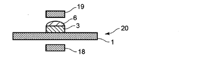
- the lens-equipped substrate 20 includes a substrate 1, a columnar member 3 provided on one surface side of the substrate 1 so as to protrude from one surface of the substrate 1, and the columnar member 3.
- the lens member 6 is provided.
- the lens member 6 is a convex lens, and its upper surface is curved in a convex shape to become a convex lens surface (see FIG. 1).
- optical members such as a light emitting element, a light receiving element, an optical waveguide, and an optical fiber are arranged at a position facing the lens member 6 and a position facing the other surface of the substrate 1. It is used for optical communication. Specifically, for example, as shown in FIG. 2, a light emitting element 18 is disposed at a position facing the other surface of the substrate 1 and coincident with the lens member 6, and a light receiving element 19 is disposed at a position facing the lens member 6. To do.
- the optical signal emitted from the light emitting element 18 enters the substrate 1 from the other surface side of the substrate 1, and the incident optical signal passes through the substrate 1, the columnar member 3, and the lens member 6, and is a convex lens of the lens member 6.
- the light is condensed by the surface and incident on the light receiving element 19.
- substrate There is no restriction
- substrate 1 For example, a glass epoxy resin substrate, a ceramic substrate, a glass substrate, a silicon substrate, a plastic substrate, a metal substrate, a substrate with a resin layer, a substrate with a metal layer, a plastic film, with a resin layer Examples thereof include a plastic film, a plastic film with a metal layer, a resin film, and an electric wiring board.
- Polyester such as polyethylene terephthalate, polybutylene terephthalate, polyethylene naphthalate; polyolefin such as polyethylene, polypropylene; polyamide, polycarbonate, polyphenylene ether, polyether sulfide, polyarylate, liquid crystal polymer, polysulfone, polyethersulfone, polyether Ether ketone, polyether imide, polyamide imide, polyimide and the like are preferable.
- those which block actinic rays for photocuring a resin for forming a columnar member and a resin for forming a lens member described later are preferable.
- the active light for photocuring the resin for forming a columnar member is ultraviolet light
- a metal substrate, a plastic substrate such as a polyimide film that does not transmit ultraviolet light, a glass epoxy resin substrate, and the like are preferable.
- the thickness of the substrate is not particularly limited, but the thickness of the substrate is preferably 5 ⁇ m to 1 mm, more preferably 10 ⁇ m to 100 ⁇ m, from the viewpoint of securing strength and reducing optical loss by shortening the optical path.
- a substrate 1 that can transmit an optical signal to be used may be used.
- a plastic substrate such as a polyimide film that transmits infrared light, A silicon substrate or the like may be used.
- the material of the lens member 6 is not particularly limited as long as it is transparent to an optical signal, but is a cured product of a photosensitive resin composition and / or a thermosetting resin composition from the viewpoint of a manufacturing method described later. It is preferable.
- the lens center position is decentered on the columnar member 3 by using a resin composition that becomes a lens shape by curing after liquefaction (drip) or a liquid resin composition. It is more preferable because it can be formed without any problems. In particular, when the viscosity of the liquid state is low, the lens center is automatically aligned with the center of the columnar member 3 on the columnar member 3.
- a convex lens shape such as a spherical surface or an aspherical surface is preferable.
- the height (thickness) of the lens member 6 is preferably 5 ⁇ m or more because it is easy to obtain a curvature as a lens, and it is preferably 150 ⁇ m or less because the thickness can be easily controlled. Further, as will be described later, when the lens member 6 is formed by photolithography, the thickness of the curved-surface-forming member 14 (thickness on the columnar member 3) to be described later is appropriately selected depending on the lens shape after dripping. That's fine.
- the photosensitive resin composition used for forming the lens member 6 (a) a binder polymer, (b) a photopolymerizable unsaturated compound having an ethylenically unsaturated group, (c) a photopolymerization initiator, The thing containing is preferable.
- This photosensitive resin composition is cured by irradiation with actinic rays, and the cured product is dripped by heating into a lens shape.
- a vinyl copolymer for example, a vinyl copolymer may be mentioned, and specifically, a polymer obtained by polymerizing the following vinyl monomer may be mentioned.
- acrylic acid, methacrylic acid, maleic acid, fumaric acid, itaconic acid methyl acrylate, methyl methacrylate, ethyl acrylate, ethyl methacrylate, n-propyl acrylate, n-propyl methacrylate, iso-propyl acrylate Iso-propyl methacrylate, n-butyl acrylate, n-butyl methacrylate, iso-butyl acrylate, iso-butyl methacrylate, sec-butyl acrylate, sec-butyl methacrylate, tert-butyl acrylate, Tert-butyl methacrylate, pentyl acrylate, pentyl methacrylate, hexyl acrylate,
- a binder polymer for example, a vinyl copolymer having a functional group such as a carboxyl group, a hydroxyl group, an amino group, an isocyanate group, an oxirane ring, an acid anhydride, etc.
- the side chain obtained by the addition reaction of a compound having one functional group such as an oxirane ring, isocyanate group, hydroxyl group, carboxyl group and at least one ethylenically unsaturated group that is bonded by reaction is ethylenic.
- a radically polymerizable copolymer having an unsaturated group can also be used.
- Examples of the vinyl monomer used in the production of the vinyl copolymer having a functional group such as carboxyl group, hydroxyl group, amino group, isocyanate group, oxirane ring, and acid anhydride include acrylic acid, methacrylic acid, and maleic acid. , Fumaric acid, itaconic acid, cinnamic acid, 2-hydroxyethyl acrylate, 2-hydroxyethyl methacrylate, acrylamide, methacrylamide, ethyl isocyanate, ethyl isocyanate, glycidyl acrylate, glycidyl methacrylate, maleic anhydride, etc. Is mentioned. These may be polymerized singly or in combination of two or more.
- the said vinyl monomers other than the vinyl monomer which has functional groups such as a carboxyl group, a hydroxyl group, an amino group, an isocyanate group, an oxirane ring, and an acid anhydride, can be copolymerized as needed.
- the weight average molecular weight of the binder polymer was heat resistance, heat meltability, coatability, and a microlens array photosensitive element described later. From the viewpoints of film properties (characteristics for maintaining a film-like form), solubility in a solvent, solubility in a developing solution in the development step, and the like, it is preferably 1000 to 300000, and 5000 to 150,000. It is more preferable. Further, (a) the binder polymer preferably has an acid value so that it can be developed with various known developing solutions.
- the acid value when developing using an aqueous alkali solution such as sodium carbonate, potassium carbonate, tetramethylammonium hydroxide, triethanolamine, etc., the acid value is preferably 50 to 260 mgKOH / g. When the acid value is 50 mgKOH / g or more, development is facilitated, and when it is 260 mgKOH / g or less, the developer resistance (the property that the portion that becomes a pattern without being removed by development is not affected by the developer) is obtained. It will be enough.
- the acid value is preferably 16 to 260 mgKOH / g. When the acid value is 16 mgKOH / g or more, development is easier, and when the acid value is 260 mgKOH / g or less, the developer resistance is more sufficient.
- the photopolymerizable unsaturated compound having an ethylenically unsaturated group for example, a compound obtained by reacting a polyhydric alcohol with an ⁇ , ⁇ -unsaturated carboxylic acid, 2,2-bis (4- (Di (meth) acryloxypolyethoxy) phenyl) propane, a compound obtained by reacting a glycidyl group-containing compound with an ⁇ , ⁇ -unsaturated carboxylic acid, a urethane monomer, nonylphenyldioxylene (meth) acrylate, ⁇ - Chloro- ⁇ -hydroxypropyl- ⁇ '-(meth) acryloyloxyethyl-o-phthalate, ⁇ -hydroxyethyl- ⁇ '-(meth) acryloyloxyethyl-o-phthalate, ⁇ -hydroxypropyl- ⁇ '-(meta ) Acryloyloxyethyl-o-phthalate
- Examples of the compound obtained by reacting the polyhydric alcohol with ⁇ , ⁇ -unsaturated carboxylic acid include, for example, polyethylene glycol di (meth) acrylate having 2 to 14 ethylene groups, and 2 propylene groups.
- polypropylene glycol di (meth) acrylate trimethylolpropane di (meth) acrylate, trimethylolpropane tri (meth) acrylate, trimethylolpropane ethoxytri (meth) acrylate, trimethylolpropane diethoxytri (meth) acrylate , Trimethylolpropane triethoxytri (meth) acrylate, trimethylolpropanetetraethoxytri (meth) acrylate, trimethylolpropane pentaethoxytri (meth) acrylate, tetramethylolmethanetri ( And (meth) acrylate (pentaerythritol tri (meth) acrylate), tetra
- Examples of the 2,2-bis (4- (di (meth) acryloxypolyethoxy) phenyl) propane include 2,2-bis (4- (di (meth) acryloxydiethoxy) phenyl) propane, 2 , 2-bis (4- (di (meth) acryloxytriethoxy) phenyl) propane, 2,2-bis (4- (di (meth) acryloxypentaethoxy) phenyl) propane, 2,2-bis (4 -(Di (meth) acryloxydecaethoxy) phenyl) and the like.
- Examples of the compound obtained by reacting the glycidyl group-containing compound with an ⁇ , ⁇ -unsaturated carboxylic acid include trimethylolpropane triglycidyl ether tri (meth) acrylate and 2,2-bis (4- (meth)). (Acryloxy-2-hydroxy-propyloxy) phenyl and the like.
- urethane monomer examples include (meth) acrylic monomers having an OH group at the ⁇ -position and isocyanate compounds such as isophorone diisocyanate, 2,6-toluene diisocyanate, 2,4-toluene diisocyanate, and 1,6-hexamethylene diisocyanate.
- isocyanate compounds such as isophorone diisocyanate, 2,6-toluene diisocyanate, 2,4-toluene diisocyanate, and 1,6-hexamethylene diisocyanate.
- Addition reaction product tris ((meth) acryloxytetraethylene glycol isocyanate) hexamethylene isocyanurate, ethylene oxide modified urethane di (meth) acrylate, propylene oxide modified urethane di (meth) acrylate and the like.
- Examples of the (meth) acrylic acid alkyl ester include (meth) acrylic acid methyl ester, (meth) acrylic acid ethyl ester, (meth) acrylic acid butyl ester, (meth) acrylic acid 2-ethylhexyl ester, and the like.
- Said photopolymerizable unsaturated compound can be used individually by 1 type or in combination of 2 or more types.
- the photopolymerization initiator generates free radicals by actinic rays.
- benzophenone N, N′-tetramethyl-4,4′-diaminobenzophenone (Michler ketone), N, N′-tetraethyl -4,4'-diaminobenzophenone, 4-methoxy-4'-dimethylaminobenzophenone, 2-benzyl-2-dimethylamino-1- (4-morpholinophenyl) -butan-1-one ("IRGACURE-369", BASF Japan Ltd., trade name), 2-methyl-1- [4- (methylthio) phenyl] -2-morpholino-propan-1-one (“Irgacure-907”, BASF Japan Inc., trade name), etc.
- Aromatic ketone 2-ethylanthraquinone, phenanthrenequinone, 2-tert-butylanthraquinone Octamethylanthraquinone, 1,2-benzanthraquinone, 2,3-benzanthraquinone, 2-phenylanthraquinone, 2,3-diphenylanthraquinone, 1-chloroanthraquinone, 2-methylanthraquinone, 1,4-naphthoquinone, 9,10- Quinones such as phenanthraquinone, 2-methyl-1,4-naphthoquinone and 2,3-dimethylanthraquinone; benzoin ether compounds such as benzoin methyl ether, benzoin ethyl ether and benzoin phenyl ether; benzoin, methyl benzoin and ethyl benzoin Benzoin compounds such as benzyl derivatives; benzyl
- the substituents substituted with two 2,4,5-triarylimidazoles may be the same or different.
- 2,4,5-triarylimidazole dimer is preferable from the viewpoint of adhesion to the columnar member 3 and sensitivity.
- 2-methyl-1- [4- (methylthio) phenyl] -2-morpholino-propan-1-one is more preferable from the viewpoint of visible light transmittance.
- Said photoinitiator can be used individually by 1 type or in combination of 2 or more types.
- the blending ratio of the (a) binder polymer is preferably 20 to 90 parts by weight, and preferably 30 to 85 parts by weight with respect to 100 parts by weight as the total of the components (a) and (b). More preferably, it is 35 to 80 parts by mass, particularly preferably 40 to 75 parts by mass.
- the blending ratio of (b) the photopolymerizable unsaturated compound having an ethylenically unsaturated group is preferably 10 to 80 parts by mass with respect to 100 parts by mass as the total of components (a) and (b).
- the blending ratio of the (c) photopolymerization initiator is preferably 0.05 to 20 parts by mass, and preferably 0.1 to 15 parts by mass with respect to 100 parts by mass of the total amount of the components (a) and (b). The amount is more preferably 0.15 to 10 parts by mass.
- the blending ratio is 0.05 parts by mass or more, photocuring is sufficient, and when it is 20 parts by mass or less, absorption of actinic rays on the actinic ray-irradiated surface of the photosensitive layer is suppressed at the time of exposure. Photocuring is sufficient.
- an adhesion imparting agent such as a silane coupling agent, a leveling agent, a plasticizer, a filler, an antifoaming agent, a flame retardant, a stabilizer, and an antioxidant.
- Fragrance, thermal crosslinking agent, polymerization inhibitor and the like can be contained. These can be used individually by 1 type or in combination of 2 or more types. Further, the blending ratio of these may be 0.01 to 20 parts by mass with respect to 100 parts by mass of the total amount of the components (a) and (b).
- the columnar member 3 is a member that protrudes from the surface of the substrate 1, and its upper surface is preferably a flat surface. As is apparent from FIG. 1, the columnar member 3 is preferably formed in a cylindrical shape in accordance with the shape of the lens member 6.
- the columnar member 3 is preferably formed separately from the substrate 1 and is formed of a transparent material having transparency to the optical signal wavelength so that the optical signal can be transmitted.
- a material of the columnar member 3 from the viewpoint of the manufacturing method mentioned later, it is preferable that it is a photosensitive resin composition, and it is more preferable that it is a hardened
- cured material of the photosensitive resin composition for forming the columnar member 3 uses what does not dripping or deform
- the temperature is preferably higher than the cured product of the lens member-forming resin composition or not melted by heating.
- the same composition as that for forming a clad or core described later can be used.
- actinic rays are irradiated from the other surface side of the substrate 1, and the lens member forming photosensitive resin composition on the columnar member 3 is exposed and cured through the columnar member 3.
- the columnar member 3 may be formed of a material that transmits actinic rays.
- the columnar member 3 can arbitrarily select the height and position of the lens member 6 by arbitrarily selecting the height from the surface of the substrate 1 (one surface of the substrate 1), and the lens member 6 and the columnar member 3.
- the shape can be selected.
- the height of the columnar member 3 from the surface of the substrate 1 is appropriately selected according to the height of the lens member formed on the columnar member 3, but if it is 5 ⁇ m or more, the lens member 6 and the surface of the substrate 1
- the distance can be secured, and is preferably 100 ⁇ m or less because the height of the columnar member 3 can be easily controlled.
- the lens-attached substrate 20 is manufactured by a manufacturing method including the following first to third steps, for example.
- 1st process The process of forming a columnar member in one surface of the said board
- the photosensitive resin composition for forming a lens member is laminated on the side, the photosensitive resin composition for forming a lens member on the columnar member is cured by exposure, and a columnar transparent member for forming a lens member is formed on the columnar member.
- the columnar member 3 is formed on one surface of the substrate 1 (see FIGS. 3B and 4B).
- the method for forming the columnar member 3 is not particularly limited, but a method in which the columnar member 3 is formed as a separate member from the substrate 1 and then attached using an adhesive or the like, or a resin composition for forming the columnar member on the substrate 1 is used. A method of laminating to a desired thickness and patterning by photolithography to form the columnar member 3 can be mentioned.
- the columnar member 3 is formed by photolithography from the viewpoint of alignment accuracy, and the columnar member-forming resin composition is a photosensitive resin, and more preferably formed by exposure and development.
- the method of laminating the resin composition for forming a columnar member on the substrate 1 is not particularly limited, but a method of applying the resin composition on the substrate 1 using a comma coater, a die coater, a spin coater or the like, or applying a resin in advance on a carrier film, It can be formed by a method of bonding by using a roll laminator, a vacuum roll laminator, a vacuum laminator, a normal pressure press, a vacuum press or the like as a dried and dried film shape.
- a lens member-forming photosensitive resin composition is laminated on one surface side of the substrate 1, and the lens member-forming photosensitive resin is formed on at least the columnar member 3.
- the forming columnar member 6A is formed (see FIGS. 3C and 4C).
- the photosensitive resin composition for forming a lens member to be laminated on one surface side of the substrate 1 is not particularly limited, but even if it is laminated only on the columnar member 3, both the columnar member 3 and the substrate 1 are laminated. It may be laminated on top.
- the method of laminating the lens member-forming photosensitive resin composition on both the columnar member 3 and the substrate 1 by a method of applying or bonding the same as in the first step is preferable.
- the method for exposing the lens member-forming photosensitive resin composition is not particularly limited as long as the photosensitive resin on the columnar member 3 can be cured.
- the lens member forming photosensitive resin composition is laminated on both the columnar member 3 and the substrate 1, the lens member forming photosensitive resin composition is exposed from the columnar member 3 to the substrate 1 surface. Then, since a desired lens shape cannot be obtained in a later step, it is necessary to expose only the photosensitive resin composition for forming a lens member laminated on the columnar member 3.
- the photosensitive resin composition for forming a lens member When the photosensitive resin composition for forming a lens member is laminated on both the columnar member 3 and the substrate 1, the uncured portion of the photosensitive resin composition for forming a lens member laminated on the substrate 1 is developed. Then, the lens member forming columnar member 6 ⁇ / b> A is formed on the columnar member 3.
- the method for removing the uncured part is not particularly limited, and the uncured part may be removed with a solvent or an alkaline solution.
- the step of developing and removing the uncured portion is unnecessary, and only the lens member-forming photosensitive resin composition is cured.
- the lens member forming columnar member 6A can be formed.
- the thickness of the lens member forming columnar member 6A may be appropriately selected according to the desired lens shape of the lens member 6.
- film thickness of the photosensitive resin composition for lens member formation (Thickness of the lens-member-forming columnar member 6A) + (thickness of the columnar member 3)
- the thickness (height) of the lens member forming columnar member 6A is substantially the same as the height of the lens member 6, and is preferably 5 ⁇ m or more and 150 ⁇ m or less.
- the columnar member-forming photosensitive resin composition and the lens member-forming photosensitive resin composition may be cured by pattern exposure using a photomask.
- a columnar member-forming resin layer or a lens member-forming photosensitive resin composition formed on the substrate 1 using the columnar member-forming photosensitive resin composition is used.
- a photomask having an opening (the shape of the opening is the same as that of the columnar member) is placed on the formed lens member forming resin layer, and actinic rays are irradiated from the photomask side, whereby the columnar member 3 and the lens member. 6 can be formed at a predetermined location.
- a photomask is disposed on the surface opposite to the surface on which the columnar member-forming resin layer or lens member-forming resin layer is formed (that is, the other surface side). Then, it is possible to form the columnar member 3 and the lens member 6 at predetermined locations by irradiating active light from the photomask side. Further, in the first step and the second step, a resin film including a laminate of a columnar member forming resin layer and a lens member forming resin layer is manufactured in advance, and this is laminated on a substrate, and photolithography processing is performed. Thus, the columnar member 3 and the lens member 6 can be formed at predetermined locations.
- the resin film used here it is preferable to laminate
- the presence of the support film facilitates the production of the curved surface pattern forming resin film, and the presence of the protective film protects the columnar member forming resin layer. Any one or both of the support film and the protective film may be provided.
- the curved shape pattern forming resin film it is easy to control the thickness of the columnar member forming resin layer and the lens member forming photosensitive resin layer (for details, refer to the curved shape pattern forming resin film described later).
- the lens member forming columnar member 6A is heated and dripped to form the upper surface of the lens member forming columnar member 6A as a convex lens surface, thereby forming the lens member 6 on the columnar member 3. Then, the lens-attached substrate 20 is obtained (see FIGS. 3D and 4D). In addition, the columnar member 3 is not melted by the heating in the third step, and the shape before the heating is maintained.
- the lens surface of the lens member 6 is adjusted to an arbitrary height from the surface of the substrate 1 by appropriately adjusting the height of the columnar member 3. It becomes possible to arrange it. For this reason, it is possible to reduce the optical loss by shortening the distance between the lens member and another optical member (for example, the light receiving element 19).
- the curvature of the convex lens surface can be arbitrarily set, and the lens member 6 having a desired shape can be easily formed.
- the dripping on the columnar member 3 is limited, and the lens member 6 can be formed without the liquefied lens member forming resin spilling from the columnar member 3. 6 is less likely to be displaced from the center position of the columnar member 3. Further, since the lens member 6 can be formed without bringing the lens member-forming resin composition into contact with the substrate 1, the lens shape varies depending on the unevenness of the substrate surface and the wettability of the lens member-forming resin composition with respect to the substrate 1. The lens member 6 can be formed without change, and a lens member having a constant shape and a constant thickness can be formed with high precision regardless of the type of the substrate 1.
- the columnar member is provided as a separate member from the substrate 1, but may be formed as a member integrated with the substrate 1.
- the columnar member is obtained by a method of forming a part of the substrate 1 by deforming it by plate pressing or the like.
- the substrate with a lens according to the second embodiment of the present invention uses a substrate 1 having a through hole 2 as a substrate, and includes a columnar member 3 and a lens member 6 on the through hole 2.
- a transparent member 5 is provided on the other surface side of the substrate 1.
- the columnar member 3 As shown in FIGS. 5 and 6, the columnar member 3 according to the present embodiment is formed so that a part thereof fills one surface side of the through hole 2 and a part protrudes from the through hole 2.
- the transparent member 5 is a member laminated on the other surface of the substrate 1, and penetrates into the through hole 2 in a portion where the through hole 2 exists, and the other surface side in the through hole 2 is covered.
- the inside of the through hole 2 is filled so that no gap is generated between the transparent member 5 and the columnar member 3.
- the inside of the through hole 2 may be filled with only one of the columnar member 3 and the transparent member 5.
- the same substrate as in the first embodiment can be used, but since an optical signal is transmitted through the through hole 2, materials other than a material having transparency to the optical signal are also used. Is possible.
- the substrate be capable of blocking actinic rays such as ultraviolet rays as in the first embodiment.
- the through hole 2 provided in the substrate 1 can be suitably formed by, for example, drilling or laser processing. Moreover, the through-hole 2 with a metal layer formed by vapor-depositing, sputtering, plating, etc. on the side surface of the through-hole 2 may be sufficient. Further, when a metal foil is provided on the outer periphery of the through hole 2 on one surface or the other surface of the substrate 1, the metal foil can be used as a light shielding portion.
- the shape in plan view orthogonal to the depth direction of the through hole 2 is not particularly limited, and may be a circular shape such as a perfect circle or an ellipse; a polygonal shape such as a triangle, a quadrangle, a pentagon, or a hexagon.
- the through hole 2 preferably has a shape that matches the shape of the lens member 6 in plan view, and is preferably formed in a circular shape such as a perfect circle.
- the space in the through hole 2 may have the same shape regardless of the position in the depth direction, or may have a tapered shape that becomes smaller or larger as it moves in the depth direction.
- the area of the through hole 2 in plan view may be in a range that does not affect the optical loss, and is preferably 600 to 800,000 ⁇ m 2 , more preferably 2500 to 200,000 ⁇ m 2 .
- Transparent material As a material for the transparent member 5, it is sufficient if the material has transparency to the optical signal wavelength. From the viewpoint of the production method to be described later, a cured product of the photosensitive resin composition or a cured product of the thermosetting resin composition is preferable. From the viewpoint that it can be formed together with the columnar member 3, a cured product of the photosensitive resin composition. It is more preferable that In addition, as described later, when the photosensitive resin composition for forming a columnar member and the photosensitive resin composition for forming a lens member are exposed and cured through the transparent member 5, these resin compositions such as ultraviolet rays are used.
- the material may be a material that transmits actinic rays that can cure the object.
- the transparent member 5 and the columnar member 3 may be connected within the through hole 2.
- the connection here means a state in which there is no gap in the through hole and the space is filled with the transparent member 5 and / or the columnar member 3.
- the thickness of the transparent member 5 is not particularly limited, but is preferably 1 ⁇ m or more because it is easy to ensure adhesion to the substrate 1, and if it is 100 ⁇ m or less, the thickness can be easily controlled.
- the thickness of 50 ⁇ m or less is more preferable because the entire thickness of the substrate with a lens can be reduced.
- the thickness of the transparent member 5 is the thickness of the transparent member 5 at a portion where the through hole 2 is not provided.
- the bottom surface of the transparent member 5 (that is, the surface opposite to the substrate-side surface of the transparent member) is formed in a plane parallel to the surface of the substrate 1 and is a non-lens surface. Therefore, when light enters the bottom surface of the transparent member 5, light scattering at the bottom surface is suppressed.
- the lens-attached substrate is manufactured by the following first to third steps.
- the manufacturing method of this embodiment will be described.
- the substrate a polyimide film that shields actinic rays for exposing the columnar member-forming photosensitive resin composition and the lens member-forming photosensitive resin composition is used. Examples are described, but not limited thereto.
- the transparent member 5 is also formed in the first step.
- a substrate 1 having a through hole 2 is prepared as a substrate (see FIGS. 7A and 8A).
- the columnar member forming photosensitive resin composition is used on one surface of the substrate 1 so that the columnar member forming photosensitive resin composition is filled into the through hole 2 from one surface side of the substrate 1.
- a columnar member-forming resin layer 3A is laminated.
- the transparent member forming resin composition is used on the other surface of the substrate 1 so that the transparent member forming resin composition is filled into the through hole 2 from the other surface side of the substrate 1.
- the resin layer 5A is laminated (see FIGS.
- the step of laminating the columnar member-forming resin layer 3A or the step of laminating the transparent member-forming resin layer 5A may be performed first or at the same time.
- the method of laminating the photosensitive resin composition for forming a columnar member and the resin composition for forming a transparent member is not particularly limited, and examples thereof include a coating method and a bonding method in the same manner as in the first step.
- the columnar member-forming photosensitive resin composition and the transparent member-forming resin composition are exposed and photocured by irradiating actinic rays from the other surface side of the substrate 1.
- the substrate 1 a substrate that shields actinic rays is used, and therefore, one surface side of the substrate 1 is not irradiated with actinic rays except for a portion having the through holes 2. Only the columnar member-forming photosensitive resin composition (columnar member-forming resin layer 3A) located at a position corresponding to is exposed. On the other hand, the entire other surface side of the substrate 1 is exposed, and the transparent member-forming resin composition (transparent member-forming resin layer 5A) is disposed in the through hole 2 and the other side of the substrate 1.
- the method for developing and removing the uncured portion is not particularly limited, and may be removed with a solvent or an alkaline solution.
- a photosensitive resin composition for forming a lens member is laminated on one surface side of the substrate 1 in the same manner as in the first embodiment, and then an actinic ray from the other surface side of the substrate 1. Irradiate.
- the actinic ray is transmitted only through the portion where the through hole 2 is present, and only the portion corresponding to the through hole 2 is cured in the lens member forming photosensitive resin composition.
- the uncured portion is developed and removed in the same manner as in the first embodiment, whereby the lens member forming columnar member 6A is formed only on the columnar member 3 (FIGS. 7D and 8D). d)).
- the lens member-forming columnar member 6A becomes the lens member 6 by dripping (heat dripping), and the substrate with lens 20 of this embodiment is obtained (FIG. 7 (e) and FIG. 8 (e)).
- the lens surface of the lens member 6 is arranged at an arbitrary height from the surface of the substrate 1 by providing the lens member 6 on the columnar member 3 as in the first embodiment. And it becomes easy to form the lens shape as desired. Further, since the inside of the through hole 2 is filled so that no gap is formed between the transparent member 5 and the columnar member 3, an optical signal is transmitted through the through hole 2 regardless of the type of the substrate 1, and the lens member 6. As a result, the optical signal can be collimated and condensed. Therefore, the lens-equipped substrate 20 according to the second embodiment can perform optical communication with little optical loss even when the substrate 1 is not a transparent substrate. Further, since the through hole 2 is provided, the columnar member 3 and the lens member 6 can be more easily aligned.
- the transparent member forming resin composition (transparent member forming resin layer 5A) is exposed simultaneously with the columnar member forming photosensitive resin composition (columnar member forming resin layer 3A).
- the transparent member forming resin composition (transparent member forming resin layer 5A) may be cured before or after being cured. Further, the curing of the transparent member forming resin composition (transparent member forming resin layer 5A) is not limited to photocuring, and may be thermosetting.
- the columnar member-forming photosensitive resin composition (columnar member-forming resin layer 3A) is used. You may expose using a photomask.
- a photomask having at least an opening larger than the through hole is placed on either side of the substrate.
- the photomask is disposed on the same side as the lens member-forming photosensitive resin composition (lens member-forming columnar member 6A) formation surface. Even if the exposure is performed, there is no particular problem even if the photomask is arranged on the surface opposite to the formation surface and the exposure is performed.
- the transparent member 5 is laminated on the entire other surface of the substrate 1 .
- the transparent member 5 is appropriately patterned to form a part of the other surface of the substrate 1. It may be laminated only on.
- the transparent member 5 may be provided only in the portion where the through hole 2 is provided and the peripheral portion thereof.
- exposure to the photosensitive resin composition for columnar member formation (columnar member formation resin layer 3A) and the transparent member formation resin composition (transparent member formation resin layer 5A) is performed. It is preferable to carry out by covering the other surface side of the substrate 1 with a photomask 23 having an opening 22 larger than the through hole 2.
- the opening 22 faces the through hole 2, and the center position of the opening 22 is made to coincide with the center position of the through hole 2.
- the transparent member-forming resin composition transparent member-forming resin layer 5A
- the transparent member 5 is exposed to the through hole 2. Only the matching part and its peripheral part are cured, and the others become uncured parts.
- the columnar member-forming photosensitive resin composition is a columnar member-forming photosensitive resin composition (columnar member-forming resin layer 3 ⁇ / b> A) at a position corresponding to the through hole 2. Only is exposed. Therefore, the columnar member 3 and the transparent member 5 shown in FIG. 9 are obtained by development removal after exposure.
- the bottom surface of the transparent member 5 disposed outside the through hole 2 may bulge downward to form a convex lens surface 15 as shown in FIG. 11, whereby the substrate 1 is a substrate with a biconvex lens. It becomes.
- the transparent member 5 is formed of a photosensitive resin composition for forming a lens member and dripped with the lens member-forming columnar member 6A by heating in the third step.
- electrical wiring may be provided on, for example, one surface of the substrate 1, and the substrate 1 may be an electrical wiring board having electrical wiring.
- the electrical wiring can be used, for example, as a light emitting / receiving element mounting electrode, a driver IC mounting electrode, or the like.
- the method for forming the electrical wiring is not particularly limited, but may be formed by a conventional method such as a semi-additive method, a subtractive method, or an additive method. Further, various metal platings may be applied to the surface of the electric wiring, and a resist 13 described later may be used as a plating resist.
- a resist 13 for protecting the lens member 6 may be provided around the lens member 6 in the first and second embodiments.
- the shape of the resist 13 in plan view of the substrate 1 is not particularly limited as long as it does not interfere with the optical signal transmitted through the lens.
- the height of the resist 13 is set to be equal to or higher than the height from one surface of the substrate 1 to the uppermost portion of the lens member 6, but is preferably larger than the height to the uppermost portion of the lens member 6.
- the resist 13 may be used as an electrical wiring protection resist or a plating resist.
- the method for forming the resist is not particularly limited, and may be performed after the lens member 6 is formed.
- the resist is formed by a method of applying or bonding a photosensitive resist forming resin in the same manner as in the first step. It can be formed later by photolithography. Forming by photolithography is more preferable because it can be formed with high positional accuracy.
- the resist may be formed from the same photosensitive resin composition for forming a lens member simultaneously with the formation of the lens member 6. In this case, the resist may be a dummy lens having a lens shape.
- optical waveguide with lens By providing the optical waveguide 10 on the substrate with a lens of the present invention, an optical waveguide with a lens can be obtained.
- the transparent member 5 is used as the lower clad layer 7, and the core layer 8 and the upper clad layer 9 are sequentially laminated thereon to form the optical waveguide 10.
- the transparent member 5 is the lower cladding layer of the optical waveguide, the optical waveguide 10 having a small thickness can be formed.
- the core layer 8 forms a core pattern composed of a plurality of elongated cores, for example, and the core pattern is disposed so as to be embedded in the lower and upper cladding layers 7 and 9.
- the optical waveguide 10 is provided with a mirror 11, and the lens member 6 and the mirror 11 are provided at positions facing each other with the substrate 1 interposed therebetween. According to this optical waveguide 10 with a lens, the optical signal propagated in the core layer 8 is optically converted by the mirror 11, and then condensed on the convex lens surface of the lens member 6 and incident on another optical member or the like. Light propagation can be performed with little optical loss.
- an optical signal that has entered the convex lens surface of the lens member 6 from the outside of the optical waveguide with lens 10 is condensed on the convex lens surface, and then converted into an optical path by the mirror 11 and propagated into the core layer 8, resulting in optical loss. Will be less.
- a groove 17 having a triangular cross section as shown in FIG. 14 is formed along the direction orthogonal to the axial direction of the core pattern from the upper clad layer 9 side of the optical waveguide 10.
- An inclined surface 17 ⁇ / b> A is formed in the optical waveguide 10.
- a core embedded in the lower and upper clad layers 7 and 9 is exposed on the inclined surface 17A, and a mirror 11 is formed by the core.
- the mirror 11 is provided in each groove 17 in the same number as the number of cores. Become.
- the grooves 17 are provided in the vicinity of both ends of the optical waveguide 10, for example, in the direction in which the core extends.
- the optical signal from the outside which is incident on the lens member 6 on one end side of the optical waveguide 10, is optically converted by the mirror 11 on one end side and propagates through the core layer 8, and the other end. After the optical path is changed again by the part-side mirror 11, it can be incident on another optical member or the like via the lens member 6 on the other end side.
- the lens-equipped substrate 20 shown in FIG. 14 includes the resist 13, but the resist 13 may be omitted.
- a clad layer forming resin composition or a clad layer forming resin film can be used as a material for the lower clad layer 7 and the upper clad layer 9.
- the resin composition for forming a clad layer used in the present invention is not particularly limited as long as it is a resin composition that has a lower refractive index than the core and is cured by light or heat, and is not limited. A thing can be used conveniently.
- the resin composition used for the resin for forming the clad layer may have the same or different components contained in the resin composition in the lower clad layer and the upper clad layer, and the refractive index of the resin composition is the same. Or different.
- the method for forming the clad layer is not particularly limited.
- the clad layer may be formed by coating the clad layer forming resin composition or laminating the clad layer forming resin film.
- the method is not limited, and the clad layer forming resin composition may be applied by a conventional method.
- the clad layer-forming resin film used for laminating can be easily produced by, for example, dissolving the clad layer-forming resin composition in a solvent, applying it to a carrier film, and removing the solvent.
- the thicknesses of the lower cladding layer and the upper cladding layer are not particularly limited, but the thickness after drying is preferably in the range of 5 to 500 ⁇ m. When the thickness is 5 ⁇ m or more, a clad thickness necessary for light confinement can be secured, and when the thickness is 500 ⁇ m or less, it is easy to control the film thickness uniformly. From the above viewpoint, the thickness of the lower cladding layer and the upper cladding layer is more preferably in the range of 10 to 100 ⁇ m.
- a resin composition for forming a core layer or a resin film for forming a core layer can be used as the core layer 8.
- the core layer forming resin composition is preferably designed to have a refractive index higher than those of the lower clad layer and the upper clad layer and capable of forming a core pattern with actinic rays.
- the method of forming the core layer before patterning is not limited, and examples thereof include a method of applying the core layer forming resin composition by a conventional method.
- the thickness of the core layer forming resin film is not particularly limited, and the thickness of the core layer after drying is usually adjusted to be 10 to 100 ⁇ m.
- the thickness of the core layer after finishing the film is 10 ⁇ m or more, there is an advantage that the alignment tolerance can be increased in the coupling with the light emitting / receiving element or the optical fiber after the formation of the optical waveguide, and when it is 100 ⁇ m or less, There is an advantage that the coupling efficiency is improved in coupling with the light emitting / receiving element or the optical fiber after the optical waveguide is formed.
- the thickness of the film is preferably in the range of 30 to 90 ⁇ m, and the film thickness may be appropriately adjusted in order to obtain the thickness.
- mirror As a method for forming the mirror, a known method can be applied. For example, it can be formed by cutting the core layer 8 using a dicing saw or the like from the upper clad layer 9 formation surface side.
- the inclination angle of the mirror 11, that is, the inclined surface 17A with respect to the axial direction of the core is preferably 45 °.
- the mirror 11 may be provided with a reflective metal layer by vapor-depositing a metal such as gold using a vapor deposition device.
- the manufacturing method of the optical waveguide with a lens is demonstrated with reference to FIG.
- the lens-attached substrate 20 provided with the transparent member 5 (lower clad layer 7) on the other surface side of the substrate 1 is formed.
- the core layer 8 and the upper clad layer 9 are sequentially laminated on the lower clad layer 7, and the optical waveguide 10 is formed on the other surface side.
- the mirror 11 is provided by forming the groove
- the manufacturing method of the optical waveguide with a mirror is not limited to this method.
- the lower and upper cladding layers are formed on the substrate with a lens on which the transparent member is not provided on the other surface side.
- the optical waveguide having the core layer and the mirror may be formed by bonding, or may be formed by providing the mirror 11 in the optical waveguide 10 after the optical waveguide is bonded.
- the lower clad layer 7, the core layer 8, and the upper clad layer 9 are sequentially laminated on the other surface of the lens-equipped substrate of the first embodiment to form an optical waveguide 10 and then a mirror 11 is provided. Also good.
- substrate with a lens and an optical waveguide with a mirror may be integrated with various optical members, such as a light receiving element and a light emitting element, and may comprise an optical module.
- the curved surface shape pattern 16 in the present invention refers to a pattern having a curved surface formed on the substrate 1, and the columnar member 3 and the curved surface shape pattern (corresponding to the lens member 6 described above) formed on the columnar member 3. Including.
- the lens member 6 of the present invention is also a kind (part) of the curved surface shape pattern (see FIG. 17D).
- the curved shape pattern of the present invention includes, for example, an optical waveguide in which the columnar member 3 is a cladding layer having a low refractive index and a portion corresponding to the lens member 6 is a core layer having a high refractive index. .
- the optical axis cross-sectional shape is close to a circle.
- an optical fiber having a circular cross section or a light receiving / emitting section is circular.
- An optical waveguide having a low coupling loss with a rectangular photodiode or laser diode can be obtained.
- an optical waveguide having a core pattern on portions corresponding to the columnar member 3 and the lens member 6 having a refractive index higher than that of the cladding layer on the cladding layer can achieve the same effect.
- a conductive layer is formed on the substrate 1
- a curved shape pattern 16 as a plating resist is formed, electroplating is performed to form an electrical wiring, and then the substrate and the conductive layer are removed.
- an electric wiring board from which the plating resist is removed can be mentioned.
- the use of the curved shape pattern 16 has an advantage that the substrate, the conductive layer, and the plating resist can be easily removed as compared with the rectangular pattern.
- the same resin composition as described above can be used. However, in the case of a curved shape that does not propagate light, the transparency of the resin is not necessary.
- the present invention includes a step (A ′) of laminating a columnar member-forming resin layer and a curved surface-forming resin layer in this order to form a laminate, the columnar member-forming resin layer, and the curved-surface-forming resin layer.
- the curved surface shape pattern forming resin film including the laminate of the curved surface shape forming resin layer 14A and the columnar member forming resin layer 3A of the present invention. It is preferable in terms of easy production.
- the resin film only needs to have a curved-surface-forming resin layer 14A that dripping (heat dripping) by heat and a columnar member forming resin layer 3A that does not dripping (heat dripping) by heat.
- the curved surface shape forming resin layer 14A that is heated by heat and the columnar member forming resin layer 3A that is not heated are either applied to one resin layer or the other resin layer prepared in advance. It is preferable to form them by bonding because the thickness can be easily controlled.
- a support film is laminated on the resin layer side for forming a curved shape, and a protective film is laminated on the resin layer side for forming a columnar member.
- the support film and the protective film may have either one or both (see FIG. 16B).
- the support film 12 is provided on the curved layer-forming resin layer 14 ⁇ / b> A side of the above laminate, it is preferable because the laminate is easy to handle. Is preferable because exposure can be performed without contaminating the photomask. From such a viewpoint, it is preferable that the support film 12 has transparency with respect to the exposure wavelength to such an extent that the patterning by exposure is not hindered.
- a protective film is provided on the columnar member-forming resin layer 3A side of the laminate because contamination of the resin surface can be suppressed.
- films of different thicknesses and materials for the support film 12 and the protective film (not shown). Thereby, the direction of the resin layer for curved shape formation and the resin layer for columnar member formation can be distinguished easily.
- the protective film can be easily peeled off. The member-forming resin layer can be easily exposed, and the chance of mistaken bonding directions is reduced, which is preferable.
- the strength of the peeling force can be determined by pulling the support film and the protective film at the same time to determine which film the resin laminate remains on, and may be left on the support film side.
- a lens or a curved surface shape pattern forming resin layer when expressed as a lens member, it refers to a portion having a function of suppressing the spread of light by changing the angle of light, or collimating or condensing light.
- the manufacturing method of the lens-attached substrate of the present invention which can be suitably manufactured when the above-described curved shape pattern forming resin film is used, will be described with reference to FIGS.
- the step (A) of laminating a substrate, a columnar member-forming resin layer, and a curved surface-forming resin layer in this order to form a laminate, the columnar member-forming resin layer and the curved surface shape Etching the forming resin layer to form a laminated convex portion of the columnar member and the curved shape forming member (B), and heating the curved shape forming member to let it drip into a lens member Step (C) is included.
- Step (A) In the present invention, as the step (A), the substrate 1, the columnar member forming resin layer 3A, and the curved surface forming resin layer 14A are combined with the substrate 1, the columnar member forming resin layer 3A, and the curved surface forming resin layer 14A. Are laminated in this order (see FIGS. 16B and 17B, but the support film is omitted here).
- the method of forming the laminate is not particularly limited, and a varnish-like columnar member-forming resin layer 3A and a varnish-like curved-surface-forming resin layer 14A are formed on the substrate 1 using a comma coater, a die coater, a spin coater, or the like.
- the film-like columnar member-forming resin layer 3A and the film-like curved-shape-forming resin layer 14A because a drying step after applying the varnish is not necessary. More preferably, after the layered body of the columnar member forming resin layer 3A and the curved surface shape forming resin layer 14A is formed in advance, the columnar member forming resin layer 3A side is stacked such that the side is the substrate 1 side. Depending on the method, the number of laminations on the substrate 1 can be reduced.
- Step (B) In the present invention, as the step (B), the columnar member-forming resin layer 3A and the curved shape-forming resin layer 14A are preferably etched at the same time, so that a laminate of the columnar member 3 and the curved shape-forming member 14 is obtained. (Laminated convex part) is formed (see FIGS. 16C and 17C).
- the etching method include dry etching such as RIE (Reactive Ion Etching), and wet etching in which a resin is dissolved or swelled and removed using a solvent or an alkaline solution.
- an etching resist pattern that is not or hardly etched is formed on the columnar member 3 and the curved shape forming member 14 to form a portion of the columnar member forming resin layer 3A and the curved shape where there is no etching resist pattern.
- a method of removing the forming resin layer 14A and then removing the etching resist pattern may be used.
- a resin that can be etched with a solution or an alkaline solution is preferably used for the columnar member-forming resin layer 3A and the curved-surface-forming resin layer 14A.
- the portions of the columnar member 3 and the curved surface forming member 14 are photocured with actinic rays and wet etched.
- the curved surface shape forming resin layer 14A is a photosensitive resin layer
- the curved surface shape forming member 14 can serve as an etching resist, and a laminate of the columnar member 3 and the curved shape forming member 14 can be formed.
- a step of forming an etching resist pattern on the curved surface shape forming resin layer 14A and a step of removing the etching resist pattern are unnecessary.
- the columnar member-forming resin layer 3A is also a photosensitive resin layer.
- the contrast between the uncured portion removed by etching and the photocured portion to be the columnar member 3 becomes clear, and the side surface of the columnar member 3 can be prevented from being scraped off.
- a laminated body of the members 14 is easily obtained.
- Step (C) In the present invention, as the step (C), the curved surface shape forming member 14 is heated and dripped (heated) to form the lens member 6 or the curved surface shape pattern 16 (laminated pattern with the columnar member 3) (FIG. 16 ( d) and FIG. 17 (d)). Since the curved surface shape forming member 14 is formed on the columnar member 3, it stays on the columnar member 3 due to surface tension even when the liquid drops (heat dripping) and the viscosity decreases. The lens member 6 or the curved shape pattern 16 can be obtained favorably without depending on the roughness.
- the temperature at which the liquid dripping (heat dripping) is not particularly limited as long as the viscosity of the curved surface shape forming member 14 decreases and the curved surface is formed, and is preferably 40 ° C. to 270 ° C., more preferably 80 ° C. to 230 ° C. ° C. From the viewpoint of maintaining the transparency of the lens member 6 and the columnar member 3, the temperature is most preferably from 80 ° C to 180 ° C. After dripping (heat dripping), heat for curing the lens member 6 and the columnar member 3 may be applied, and the temperature may be the same as or higher than the above, but the transparency of the lens member 6 and the columnar member 3 is also acceptable. Most preferably, the temperature is 80 ° C. to 180 ° C. from the viewpoint of maintaining the temperature.
- Example 1 A mirrored substrate corresponding to the first embodiment was prepared and evaluated by the following procedure. However, in Example 1, 20 lens members 6 were provided on the substrate 1.
- [Preparation of resin film for forming clad layer] ⁇ (A) Base polymer; Production of (meth) acrylic polymer (A-1)> 46 parts by mass of propylene glycol monomethyl ether acetate and 23 parts by mass of methyl lactate were weighed in a flask equipped with a stirrer, a cooling pipe, a gas introduction pipe, a dropping funnel, and a thermometer, and stirred while introducing nitrogen gas. .
- the liquid temperature was raised to 65 ° C., 47 parts by weight of methyl methacrylate, 33 parts by weight of butyl acrylate, 16 parts by weight of 2-hydroxyethyl methacrylate, 14 parts by weight of methacrylic acid, 2,2′-azobis (2,4-dimethylvaleronitrile )
- a mixture of 3 parts by mass, 46 parts by mass of propylene glycol monomethyl ether acetate and 23 parts by mass of methyl lactate was added dropwise over 3 hours, followed by stirring at 65 ° C. for 3 hours, and further stirring at 95 ° C. for 1 hour.
- a (meth) acrylic polymer (A-1) solution solid content: 45% by mass
- the acid value was calculated from the amount of 0.1 mol / L potassium hydroxide aqueous solution required to neutralize the solution (A-1). At this time, the point at which the phenolphthalein added as an indicator changed color from colorless to pink was defined as the neutralization point.
- ⁇ Preparation of a resin film for forming a cladding layer> The resin varnish for forming a clad layer obtained above is coated on a non-treated surface of a PET film (“Cosmo Shine A4100” manufactured by Toyobo Co., Ltd., thickness 50 ⁇ m) as a carrier film. MC, manufactured by Hirano Tech Seed Co., Ltd.), dried at 100 ° C. for 20 minutes, and then a surface release treatment PET film (“Purex A31” manufactured by Teijin DuPont Films Co., Ltd., 25 ⁇ m thick) is pasted as a cover film. A resin film for forming a cladding layer was obtained.
- the thickness of the resin film for forming a clad layer can be arbitrarily adjusted by adjusting the gap of the coating machine, and is described in the examples.
- the film thickness of the upper clad layer forming resin film described in the examples is the film thickness after coating.
- A) As base polymer 26 parts by mass of phenoxy resin (trade name: Phenototo YP-70, manufactured by Toto Kasei Co., Ltd.), (B) 9,9-bis [4- (2-acryloyl) as a photopolymerizable compound Oxyethoxy) phenyl] fluorene (trade name: A-BPEF, Shin-Nakamura Chemical Co., Ltd.) 36 parts by mass, and bisphenol A type epoxy acrylate (trade name: EA-1020, Shin-Nakamura Chemical Co., Ltd.) 36 mass (C) As a photopolymerization initiator, 1 part by mass of bis (2,4,6-trimethylbenzoyl) phenylphosphine oxide (trade name: Irgacure 819, manufactured by BASF Japan Ltd.), and 1- [4- ( 2-hydroxyethoxy) phenyl] -2-hydroxy-2-methyl-1-propan-1-one (trade name:
- the resin layer varnish B for core layer formation obtained above is placed on the non-treated surface of a PET film (trade name: Cosmo Shine A1517, manufactured by Toyobo Co., Ltd., thickness: 16 ⁇ m) as a carrier film, After applying and drying in the same manner, a release PET film (trade name: PUREX A31, Teijin DuPont Films Co., Ltd., thickness: 25 ⁇ m) is pasted as a cover film so that the release surface is on the resin side. A resin film for layer formation was obtained. At this time, the thickness of the resin layer can be arbitrarily adjusted by adjusting the gap of the coating machine.
- the thickness of the resin film for forming the core layer used in this example is described in the examples.
- the film thickness of the core layer forming resin film described in the examples is the film thickness after coating.
- a polyethylene terephthalate film having a thickness of 16 ⁇ m is used as a carrier film, and the photosensitive resin composition solution for lenses obtained above is uniformly applied on the carrier film using a comma coater, and is heated with a 100 ° C. hot air convection dryer. The solvent was removed by drying for 3 minutes to form a lens member-forming resin layer 6.
- the thickness of the photosensitive resin composition (film) for the lens used is described in the examples.
- the film thickness of the photosensitive resin composition for lenses described in the examples is the film thickness after coating.
- a polyethylene terephthalate film having a thickness of 25 ⁇ m was further bonded as a cover film on the obtained lens member forming resin layer 6 to prepare a lens member forming photosensitive resin film.
- thermocompression bonding was performed under the conditions of a pressure of 0.4 MPa, a temperature of 110 ° C., and a pressurization time of 30 seconds. And laminated.
- a negative photomask having a circular opening with a diameter of 210 ⁇ m, ultraviolet light is exposed from the side of the clad layer forming resin film mounting surface by an ultraviolet exposure machine (model name: EXM-1172, manufactured by Oak Manufacturing Co., Ltd.) (Wavelength 365 nm) was irradiated at 0.3 J / cm 2 .
- the carrier film was peeled off, etched using a 1.0% by mass aqueous solution of potassium carbonate, and dried at 170 ° C. for 1 hour to form the columnar member 3 (FIGS. 3B and 4B). )reference).
- the opening is positioned on the columnar member 3 through a negative photomask having a circular opening having a diameter of 200 ⁇ m, and an ultraviolet exposure machine (model name: EXM-) is formed from the photosensitive resin forming surface side for forming the lens member. 1172, manufactured by Oak Manufacturing Co., Ltd.), ultraviolet rays (wavelength 365 nm) were irradiated at 0.3 J / cm 2 .
- the carrier film of the lens member-forming photosensitive resin film was peeled off and etched using a 1.0% by mass potassium carbonate aqueous solution of a developer to form a lens member-forming columnar member 6A (FIG. 3C).
- the resin film for forming a resist As the resin film for forming a resist, the 56 ⁇ m-thick resin film for forming a clad layer obtained above is peeled off from each cover film. (Thickness: 25 ⁇ m). After that, using a vacuum pressurizing laminator (MVLP-500, manufactured by Meiki Seisakusho Co., Ltd.), after vacuuming to 500 Pa or less, thermocompression bonding was performed under the conditions of a pressure of 0.4 MPa, a temperature of 110 ° C., and a pressurization time of 30 seconds. And laminated.
- MVLP-500 vacuum pressurizing laminator
- ultraviolet rays are emitted from the clad layer forming surface side (model name: EXM-1172, manufactured by Oak Manufacturing Co., Ltd.) through a negative photomask having a square light-shielding portion with a side of 300 ⁇ m (wavelength 365 nm).
- a negative photomask having a square light-shielding portion with a side of 300 ⁇ m (wavelength 365 nm).
- the carrier film was peeled off, etched using a 1.0% by mass aqueous solution of potassium carbonate, and dried at 170 ° C. for 1 hour to form a resist 13 for protecting the lens (FIGS. 12 and 13). reference).
- the lens member 6 had a diameter of 210 ⁇ m, a height of 30 ⁇ m, and a radius of curvature of the convex lens surface was 200 ⁇ m.
- the columnar member 3 had a height of 25 ⁇ m and a flat upper surface (a contact surface with the lens member 6).
- the height of the resist 13 from one surface of the substrate was 56 ⁇ m.
- a GI50 multimode optical fiber is disposed as a light receiving optical fiber at a position facing the lens member 6, and a GI62.5 multimode optical fiber is disposed as a light emitting optical fiber at a position facing the columnar member 3.
- an optical signal of 850 nm emitted from the emission optical fiber was received by the light reception optical fiber via the substrate 1, the columnar member 3, and the lens member 6, and the light propagation loss at that time was measured.
- the light propagation loss was 0.48 dB when the distance between the optical fiber tips was 100 ⁇ m. Further, when the distance between the optical fiber tips was 200 ⁇ m, it was 0.56 dB, and optical signal transmission was possible.
- Example 2 A substrate with a lens was prepared in the same manner as in Example 1, except that the thickness of the resin film for forming columnar members was 50 ⁇ m, the thickness of the resin film for forming lens members was 75 ⁇ m, and the thickness of the resist was 81 ⁇ m.
- the lens member 6 had a diameter of 210 ⁇ m, a height of 30 ⁇ m, and the convex lens surface had a curvature radius of 200 ⁇ m.
- the columnar member 3 had a height of 50 ⁇ m from one surface of the substrate and a flat upper surface. On the other hand, the height of the resist 13 from one surface of the substrate was 81 ⁇ m.
- Example 3 A substrate with a lens was produced in the same manner as in Example 1 except that an electrical wiring board in which a Cu electrode was produced on one surface of the substrate 1 by a subtractive method was used.
- the lens member 6 had a diameter of 210 ⁇ m, a height of 30 ⁇ m, and a curvature radius of the convex lens surface of 200 ⁇ m.
- the columnar member 3 had a height of 25 ⁇ m and a flat upper surface. On the other hand, the height of the resist 13 from one surface of the substrate was 56 ⁇ m.
- Comparative Example 1 A substrate with a lens was produced in the same manner as in Example 3, except that the columnar member 3 was not formed, the thickness of the lens member-forming resin film was 25 ⁇ m, and the thickness of the resist was 31 ⁇ m. [Evaluation] When the cross section of the obtained substrate with a lens was observed, the lens member 6 had a diameter of 250 ⁇ m, a height of 20 ⁇ m, and a variation in the radius of curvature.
- Example 4 [Production of substrate with through hole] A through hole having a diameter of 210 ⁇ m was formed by drilling on a 150 mm ⁇ 150 mm polyimide film (trade name; Upilex RN, thickness: 25 ⁇ m, manufactured by Ube Nitto Kasei Co., Ltd.) as the substrate 1 to obtain a substrate with a through hole. (See FIG. 7A and FIG. 8A).
- a 150 mm ⁇ 150 mm polyimide film trade name; Upilex RN, thickness: 25 ⁇ m, manufactured by Ube Nitto Kasei Co., Ltd.
- the through hole 2 is filled with the transparent member forming resin and the columnar member forming resin, and at the same time, the transparent member forming resin is provided on one surface of the substrate 1 and the columnar member forming resin is provided on the other surface.
- Were stacked see FIGS. 7B and 8B).
- the transparent member forming resin surface side is covered with a negative type photomask having a square opening with a side of 5 mm, the center of the through hole 2 being aligned with the center of the opening, and through the photomask, Ultraviolet rays (wavelength 365 nm) were irradiated from the transparent member forming resin surface side by 0.3 J / cm 2 using the above-described ultraviolet exposure machine (see FIG. 10). The ultraviolet rays were transmitted through the opening and applied to the transparent member forming resin, and at the substrate, only the through holes were transmitted, and the columnar member forming resin was applied to the resin.
- a negative type photomask having a square opening with a side of 5 mm, the center of the through hole 2 being aligned with the center of the opening, and through the photomask, Ultraviolet rays (wavelength 365 nm) were irradiated from the transparent member forming resin surface side by 0.3 J / cm 2 using the above-described ultraviolet exposure machine (
- the transparent member-forming resin film and the columnar member-forming resin film carrier film are peeled off, etched using a 1.0% by mass potassium carbonate aqueous solution of a developer, and dried at 170 ° C. for 1 hour to obtain a transparent member. 5 and the substrate 1 with the columnar member 3 were produced.
- a photosensitive resin film for forming a lens member is laminated on one surface side of the substrate in the same manner as in Example 1, and then the ultraviolet light is applied to the substrate 1 from the transparent member 5 side using the ultraviolet exposure machine. (Wavelength 365 nm) was irradiated at 0.3 J / cm 2 . The ultraviolet rays were transmitted only through the portions where the through holes were provided, and only the portions corresponding to the through holes were cured in the lens member forming photosensitive resin film. Then, after peeling off the carrier film of the photosensitive resin film for lens member formation, it etched like Example 1, and formed the columnar member 6A for lens member formation on the columnar member 3.
- the lens member 6 had a diameter of 210 ⁇ m, a height of 30.5 ⁇ m, and a curvature radius of the upper surface of 210 ⁇ m.
- the columnar member 3 had a height of 25 ⁇ m from one surface of the substrate 1 and a flat upper surface.
- the height of the resist from one surface of the substrate was 56 ⁇ m.
- the optical propagation loss was measured as in the first example. The light propagation loss was 0.45 dB when the distance between the optical fiber tips was 100 ⁇ m. Further, when the distance between the optical fiber tips was 200 ⁇ m, it was 0.57 dB, and optical signal transmission was possible.
- Example 5 A substrate with a lens was produced in the same manner as in Example 4 except that the thickness of the resin film for forming columnar members was 50 ⁇ m, the thickness of the resin film for forming lens members was 75 ⁇ m, and the thickness of the resist was 81 ⁇ m.
- the lens member 6 had a diameter of 210 ⁇ m, a height of 30.5 ⁇ m, and a radius of curvature of the convex lens surface was 210 ⁇ m.
- the columnar member 3 had a height from one surface of the substrate of 50 ⁇ m and a flat upper surface. The height of the resist 13 from one surface of the substrate was 81 ⁇ m.
- Example 6 In Example 4, a substrate with a lens was produced in the same manner except that an electric wiring board in which a Cu electrode was produced on one surface of the substrate 1 by a subtractive method was used.
- the lens member 6 When the cross section of the obtained substrate with a lens was observed, the lens member 6 had a diameter of 210 ⁇ m, a height of 30.5 ⁇ m, and a curvature radius of the convex lens surface of 210 ⁇ m.
- the columnar member 3 had a height from one surface of the substrate of 25 ⁇ m and a flat upper surface.
- the height of the resist 13 from one surface of the substrate was 56 ⁇ m.
- Example 7 In Example 4, the transparent member-forming resin film was changed to a lens member-forming resin film, and the shape of the opening of the negative photomask used for exposure for forming the columnar member 3 was changed to a diameter of 300 ⁇ m.
- the bottom surface of the transparent member was also made into a convex lens surface by heat dripping (see FIG. 11). [Evaluation] When the cross section of the obtained substrate with a lens was observed, the lens member 6 had a diameter of 210 ⁇ m, a height of 30.5 ⁇ m, and a curvature radius of the convex lens surface of 210 ⁇ m.
- the columnar member 3 had a height from one surface of the substrate of 25 ⁇ m and a flat upper surface. The height of the resist 13 from one surface of the substrate was 56 ⁇ m.
- the transparent member on the surface opposite to the surface on which the columnar member 3 is formed also has a lens shape.
- Example 6 a substrate with a lens was produced in the same manner except that the columnar member 3 was not formed, the thickness of the resin film for forming a lens member was 25 ⁇ m, and the thickness of the resist was 31 ⁇ m.
- the diameter was 270 ⁇ m
- the cross-sectional shape was 20 ⁇ m high
- the radius of curvature varied.
- Example 8 [Optical waveguide with lens]
- the resin film for forming a transparent member was changed to a resin film for forming a lens member, and the same method was used except that the entire surface of the substrate 1 was exposed without using the negative photomask used for the exposure for forming the columnar member 3.
- a substrate with a lens was produced (see FIG. 15A).
- a roll laminator manufactured by Hitachi Chemical Technoplant Co., Ltd., HLM-1500 is laminated under the conditions of pressure 0.4 MPa, temperature 50 ° C., laminating speed 0.2 m / min, and then the above-described vacuum pressure laminator (MVLP-500, manufactured by Meiki Seisakusho Co., Ltd.) After vacuuming to 500 Pa or less, thermocompression bonding was performed under the conditions of a pressure of 0.4 MPa, a temperature of 70 ° C., and a pressurization time of 30 seconds to form a core-forming resin layer.
- MVLP-500 vacuum pressure laminator
- ultraviolet rays (wavelength 365 nm) were irradiated at 3.0 J / cm 2 from the carrier film side of the resin film for forming a clad layer using the above ultraviolet exposure machine, and the carrier film was peeled off, and then exposed at 80 ° C. for 5 minutes. Post heating was performed to form the upper cladding layer 9 (see FIG. 15C).
- Example 9 The lens member shown in FIGS. 16 and 17 was produced and evaluated by the following procedure. ⁇ Preparation of columnar member-forming resin layer (dry film)> As the columnar member-forming resin varnish, the columnar member-forming resin layer (dry film) was prepared by the following procedure using the cladding layer-forming resin varnish obtained in Example 1.
- a columnar member-forming resin varnish of a PET film (“Cosmo Shine A4100” manufactured by Toyobo Co., Ltd., thickness 50 ⁇ m) which is a support film (used as a protective film after being laminated with a curved-surface-shaped resin layer described later)
- a coating machine Multicoater TM-MC, manufactured by Hirano Techseed Co., Ltd.
- surface-released PET film Teijin DuPont Film Co., Ltd.
- the thickness of the columnar member-forming resin layer 3A (film) can be arbitrarily adjusted by adjusting the gap of the coating machine, and is described in the examples.
- the film thickness of the columnar member-forming resin layer 3A described in the examples is the film thickness after coating and drying.
- the lens member forming photosensitive resin (film) of Example 1 was used as the curved surface shape forming resin layer 14A (dry film).
- the laminate remained on the support film on the curved-surface-forming resin layer 14A side.
- the support film on the columnar member forming resin layer 3A side was used as a protective film for a laminate of the curved shape forming resin layer 14A and the columnar member forming resin layer 3A.
- Step A The protective film of the laminate of the curved surface shape forming resin layer and the columnar member forming resin layer obtained above is peeled off, and a 150 mm ⁇ 150 mm polyimide film (polyimide; Upilex RN (manufactured by Ube Nitto Kasei Co., Ltd.), thickness 25 ⁇ m).
- a vacuum pressurizing laminator MVLP-500, manufactured by Meiki Seisakusho Co., Ltd.
- vacuuming is performed to 500 Pa or less, followed by thermocompression bonding under conditions of a pressure of 0.4 MPa, a temperature of 80 ° C., and a pressurization time of 30 seconds. And laminated (see FIGS. 16B and 17B).
- Step B Subsequently, UV light (wavelength 365 nm) was reduced to 0.1 nm from the support film side through a negative photomask having a circular opening with a diameter of 210 ⁇ m by a UV exposure machine (model name: EXM-1172, manufactured by Oak Manufacturing Co., Ltd.). Irradiated with 3 J / cm 2 . Thereafter, the support film was peeled off, etched using a 1.0% by mass aqueous solution of potassium carbonate, and dried at 170 ° C. for 1 hour to form a laminate of the columnar member 3 and the curved shape forming member 14 ( FIG. 16 (c) and FIG. 17 (c)).
- Step C Thereafter, heating was performed at 180 ° C. for 1 hour, and the curved surface shape forming member 14 was dripped (heated) to form the lens member 6 on the columnar member 3 (see FIGS. 16D and 17D). .
- the diameter was 210 ⁇ m
- the cross-sectional shape was 30 ⁇ m high
- the radius of curvature was 200 ⁇ m.
- the cross-sectional shape on the columnar member 3 side was flat with the height from the substrate plane being 25 ⁇ m.
- An optical signal of 850 nm is incident from the columnar member 3 side using a GI50 multimode optical fiber for the incident portion, and the GI62.5 multimode optical fiber installed on the lens member 6 side for the light receiving portion is used as the tip of the optical fiber.
- the distance was 100 ⁇ m
- the light propagation loss was 0.45 dB.
- the distance between the optical fiber tips was 200 ⁇ m, it was 0.53 dB, and optical signal transmission was possible.
- Example 10 On the 150 mm ⁇ 150 mm polyimide film (polyimide; Upilex RN (manufactured by Ube Nitto Kasei Co., Ltd.), thickness: 25 ⁇ m), the protective film of the 25 ⁇ m-thick columnar member-forming resin layer 3A obtained above is peeled off and vacuumed Using a pressure laminator (MVLP-500, manufactured by Meiki Seisakusho Co., Ltd.), vacuuming was performed to 500 Pa or less, and then thermocompression bonding was performed under conditions of a pressure of 0.4 MPa, a temperature of 80 ° C., and a pressurization time of 30 seconds.
- MVLP-500 manufactured by Meiki Seisakusho Co., Ltd.
- the protective film of the curved surface shape forming resin layer 14A having a thickness of 30 ⁇ m was peeled off, and the columnar member forming resin layer 3A from which the support film was peeled was evacuated to 500 Pa or less using the vacuum laminator, and then the pressure was reduced to 0.
- the thermocompression bonding was performed under the conditions of 4 MPa, a temperature of 80 ° C., and a pressing time of 30 seconds.
- the lens member 6 on the columnar member 3 was formed in the same manner as in Example 1.
- the diameter was 210 ⁇ m
- the cross-sectional shape was 30 ⁇ m high
- the radius of curvature was 200 ⁇ m.
- the cross-sectional shape on the columnar member 3 side was flat with the height from the substrate plane being 25 ⁇ m.
- An optical signal of 850 nm is incident from the transparent member 5 side using the GI50 multimode optical fiber for the incident portion, and the GI62.5 multimode optical fiber installed on the lens member 6 side for the light receiving portion is used as the tip of the optical fiber.
- the distance was 100 ⁇ m
- the light propagation loss was 0.46 dB.
- the distance between the optical fiber tips was 200 ⁇ m, it was 0.51 dB, and optical signal transmission was possible.
- Comparative Example 3 A substrate with a lens was produced in the same manner as in Example 9 except that the columnar member 3 was not formed and the thickness of the curved-surface-forming resin layer was 25 ⁇ m. [Evaluation] As a result of observing the lens member 6, the diameter was 250 ⁇ m, the cross-sectional shape was 20 ⁇ m high, and the curvature radius varied.
- the distance between the lens and another optical member can be reduced or the pitch of the lens can be reduced by making the lens shape constant and desired while arbitrarily selecting the lens height. It is possible to provide a substrate with a lens that can be used.
Landscapes
- Physics & Mathematics (AREA)
- General Physics & Mathematics (AREA)
- Optics & Photonics (AREA)
- Engineering & Computer Science (AREA)
- Plasma & Fusion (AREA)
- Thermal Sciences (AREA)
- Microelectronics & Electronic Packaging (AREA)
- Optical Integrated Circuits (AREA)
Abstract
Description
例えば、特許文献1には、表面に光学素子を備えたICチップの上方に光導波路フィルムを設置し、これらICチップと光導波路フィルムとの間で光通信を行うことが開示されている。ところが、特許文献1のように光学素子のような光通信手段を備えた基板と光導波路のような光通信手段との間で光通信を行う場合、これら光通信手段同士を高精度に位置決めして実装しないと光通信することができないという問題や、集光しないと光損失が多くなり、信号強度が減少してしまう問題がある。
また、マイクロレンズの別の簡易的な製造方法としては、液滴樹脂を基板上に滴下して形成する方法も知られている。
また、光損失を少なくするために、基板上に設けたレンズ部材の厚さを大きくして、レンズ部材と、そのレンズ部材に光学的に接続される他の光学部材との距離を縮めることが考えられている。しかし、特許文献2のように熱だれによって製造したレンズでは、レンズ厚さを大きくすると、レンズ面の曲率が減少することになるから、曲率を適切に保つためには径を大きくせざるを得ず、狭ピッチ化が一層困難になる。
これらの問題は、特許文献2のように熱だれを用いたレンズ部材だけでなく、液滴樹脂を基板上に滴下してレンズ部材を形成する場合、及びレンズ形状のレジストを作製した後に異方性エッチングによって基板そのものにレンズ部材を形成する場合でも同様に生じる。さらには、別のレンズ部材として、射出成型によって台座から凸レンズが突出したマイクロレンズもあるが、この場合だと、台座の厚み分レンズ部材が厚くなり、基板とレンズ部材とを複合すると厚みが厚くなってしまう問題がある。
したがって、従来、簡単な方法で、レンズ高さを任意に選択しつつ、レンズを一定かつ所望の形状にし、例えばレンズと他の光学部材との距離を狭くしたり、レンズを狭ピッチ化したりすることは困難であった。
[1]基板と、前記基板の一方の面側に設けられる柱状部材と、前記柱状部材の上にさらに設けられるレンズ部材とを備えるレンズ付き基板、
[2]前記柱状部材が前記基板の一方の面より突出している上記[1]に記載のレンズ付き基板、
[3]前記柱状部材が透明材料で形成される上記[1]又は[2]に記載のレンズ付き基板、
[4]前記基板がスルーホールを有するとともに、前記柱状部材は、前記スルーホールの内部に一部が配置されるとともに、一部がその内部から前記基板の一方の面より突出するように形成されており、前記レンズ付き基板は、前記スルーホールの内部において前記柱状部材よりも前記基板の他方の面側に配置される透明部材を有する、上記[1]~[3]のいずれかに記載のレンズ付き基板、
[5]前記透明部材の基板側の面とは反対側の面が、前記基板の一方の面と平行な非レンズ面となっている上記[4]に記載のレンズ付き基板、
[6]前記透明部材の基板側の面とは反対側の面が、前記スルーホールの外部に配置され、凸レンズ面となっている上記[4]に記載のレンズ付き基板、
[7]前記レンズ部材が、凸レンズである上記[1]~[6]のいずれかに記載のレンズ付き基板、
[8]前記基板が、電気配線を有する電気配線板である上記[1]~[7]のいずれかに記載のレンズ付き基板、
[9]前記基板の一方の面上に、前記基板の一方の面から前記レンズ部材の最上部までの高さ以上の高さを有するレジストがレンズ部材に並設された上記[1]~[8]のいずれかに記載のレンズ付き基板、
[10]下記第1~第3工程を含む上記[1]~[9]のいずれかに記載のレンズ付き基板の製造方法、
第1工程:基板の一方の面に柱状部材を形成する工程;
第2工程:前記基板の一方の面側に、レンズ部材形成用感光性樹脂組成物を積層し、少なくとも前記柱状部材の上にレンズ部材形成用感光性樹脂組成物を配置させるとともに、露光により前記柱状部材上の前記レンズ部材形成用感光性樹脂組成物を硬化し、前記柱状部材上にレンズ部材形成用柱状部材を形成する工程;
第3工程:前記レンズ部材形成用柱状部材を加熱し、液だれさせてその上面を凸レンズ面に形成する工程
[11]前記基板が、スルーホールを有する基板であって、前記第1工程において、柱状部材形成用感光性樹脂組成物を、前記基板の一方の面側から積層しつつ前記スルーホール内に充填するとともに、透明部材形成用樹脂組成物を、前記基板の他方の面側から積層しつつ前記スルーホール内に充填し、前記スルーホールに一致した位置にある前記柱状部材形成用感光性樹脂組成物を露光して硬化すると共に、前記透明部材形成用樹脂組成物を光硬化又は熱硬化し、前記柱状部材形成用感光性樹脂組成物の未硬化部分を現像除去し、前記スルーホールの内部から前記基板の一方の面の外方に向かって突出する柱状部材を形成する上記[10]に記載のレンズ付き基板の製造方法、
[12]前記第1工程において、前記基板の他方の面側に、前記スルーホールと対向する位置に開口部を有するマスクを配置し、前記他方の面側から前記マスクを介して活性光線を照射することにより、前記柱状部材形成用感光性樹脂組成物を露光して硬化する上記[11]に記載のレンズ付き基板の製造方法、
[13]前記基板が前記柱状部材形成用感光性樹脂組成物を露光する際の活性光線に対して遮光性を有するものであり、前記第1工程において、前記基板の他方の面側から活性光線を照射することにより、前記柱状部材形成用感光性樹脂組成物のうち、前記スルーホールに一致する位置に配置される部分を露光して硬化する上記[11]に記載のレンズ付き基板の製造方法、
[14]前記第2工程において、前記基板の他方の面側に、前記スルーホールと対向する位置に開口部を有するマスクを配置し、前記他方の面側から前記マスクを介して活性光線を照射することにより、前記レンズ部材形成用感光性樹脂組成物を露光して硬化する上記[11]~[13]のいずれかに記載のレンズ付き基板の製造方法、
[15]前記基板が前記レンズ部材形成用感光性樹脂組成物を露光する際の活性光線に対して遮光性を有するものであり、前記第2工程において、前記基板の他方の面側から活性光線を照射することにより、前記レンズ部材形成用感光性樹脂組成物のうち前記スルーホールに一致する部分を露光して硬化する上記[11]~[13]のいずれかに記載のレンズ付き基板の製造方法、
[16]前記透明部材形成用樹脂組成物が感光性樹脂組成物である上記[11]~[15]のいずれかに記載のレンズ付き基板の製造方法、
[17]上記[1]~[8]のいずれかに記載のレンズ付き基板と、前記基板の他方の面側に設けられる下部クラッド層と、前記下部クラッド層上に設けられるコア層と、前記コア層上に設けられる上部クラッド層とからなる光導波路と、前記光導波路のレンズ部材と対向する位置に形成するミラーとを備えるレンズ付き光導波路、
[18]上記[4]に記載のレンズ付き基板を備え、前記透明部材が前記基板の他方の面に積層された下部クラッド層となり、前記下部クラッド層の上にコア層、及び上部クラッド層が積層されて光導波路が形成され、前記光導波路のレンズ部材と対向する位置にミラーが形成されるレンズ付き光導波路、
[19]上記[1]~[9]のいずれかに記載のレンズ付き基板を有する光モジュール、
[20]基板と、柱状部材形成用樹脂層と、曲面形状形成用樹脂層とを、この順に積層して積層体とする工程(A)、該柱状部材形成用樹脂層と該曲面形状形成用樹脂層とをエッチングして、柱状部材と曲面形状形成用部材との積層凸部を形成する工程(B)、及び該曲面形状形成用部材を加熱し、液だれさせてレンズ部材にする工程(C)を有する上記[1]~[8]のいずれかに記載のレンズ付き基板の製造方法、
[21]前記曲面形状形成用樹脂層が感光性の樹脂層である上記[20]に記載のレンズ付き基板の製造方法、
[22]前記柱状部材形成用樹脂層が感光性の樹脂層である上記[20]又は[21]に記載のレンズ付き基板の製造方法、
[23]前記工程(B)において前記曲面形状形成用樹脂層を露光によって光硬化し、次いでエッチングしてパターン化する上記[20]~[22]のいずれかに記載のレンズ付き基板の製造方法、
[24]前記工程(B)において前記曲面形状形成用樹脂層の露光と同時に前記柱状部材形成用樹脂層を露光する上記[20]~[23]のいずれかに記載のレンズ付き基板の製造方法、
[25]前記曲面形状形成用樹脂層及び前記柱状部材形成用樹脂層の少なくとも一方がドライフィルムにより形成された樹脂層である上記[20]~[24]のいずれかに記載のレンズ付き基板の製造方法、
[26]前記基板が透明基板である上記[20]~[25]のいずれかに記載のレンズ付き基板の製造方法、
[27]前記工程(A)において、あらかじめ製造された、曲面形状形成用樹脂層及び柱状部材形成用樹脂層の積層体を含む曲面形状パターン形成用樹脂フィルムを基板に積層する上記[20]~[26]のいずれかに記載のレンズ付き基板の製造方法、
[28]前記曲面形状パターン形成用樹脂フィルムが、曲面形状形成用樹脂層側に積層された支持フィルム及び前記柱状部材形成用樹脂層側に積層された保護フィルムの少なくとも一方を有する上記[27]に記載のレンズ付き基板の製造方法、
[29]前記上記[20]~[28]のいずれかに記載の製造方法によって得られたレンズ付き基板、
[30]柱状部材形成用樹脂層と曲面形状形成用樹脂層とを、この順に積層して積層体とする工程(A’)、該柱状部材形成用樹脂層と該曲面形状形成用樹脂層とをエッチングして、柱状部材と曲面形状形成用部材との積層凸部を形成する工程(B)、及び該曲面形状形成用部材を加熱し、液だれさせて曲面を形成する工程(C’)を有する、曲面形状パターンの製造方法、
[31]曲面形状形成用樹脂層及び柱状部材形成用樹脂層の積層体を含む曲面形状パターン形成用樹脂フィルム、
[32]前記曲面形状形成用樹脂層側に積層された支持フィルム及び前記柱状部材形成用樹脂層側に積層された保護フィルムの少なくとも一方を有する上記[31]に記載の曲面形状パターン形成用樹脂フィルム、
[33]基板と、該基板の一方の面側に設けられる柱状部材と、該柱状部材の上にさらに設けられる曲面形状パターンとを備える曲面形状パターン付き基板、
を提供するものである。
2 スルーホール
3 柱状部材
3A 柱状部材形成用樹脂層
5 透明部材
5A 透明部材形成用樹脂層
6 レンズ部材
6A レンズ部材形成用柱状部材
7 下部クラッド層
8 コア層
9 上部クラッド層
10 光導波路
11 ミラー
12 支持フィルム
13 レジスト
14 曲面形状形成用部材
14A 曲面形状形成用樹脂層
15 凸レンズ面
16 曲面形状パターン
17 溝
17A 傾斜面
18 発光素子
19 受光素子
20 レンズ付き基板
22 開口部
23 フォトマスク
<レンズ付き基板>
本発明の第1の実施形態に係るレンズ付き基板20は、基板1と、基板1の一方の面から突出するように基板1の一方の面側に設けた柱状部材3と、柱状部材3上に配置されるレンズ部材6とを備えるものである。レンズ部材6は、凸レンズであり、その上面が凸状に湾曲して凸レンズ面となるものである(図1参照)。
具体的には、例えば図2に示すように、基板1の他方の面に対向し、かつレンズ部材6に一致する位置に発光素子18を、レンズ部材6に対向する位置に受光素子19を配置する。発光素子18から放出された光信号は、基板1の他方の面側から基板1に入射し、入射した光信号は、基板1、柱状部材3及びレンズ部材6を通って、レンズ部材6の凸レンズ面によって集光され、受光素子19に入射される。このような構成をとることによって、少ない光ロスにて光通信を行うことができる。
(基板)
基板1の材料としては、特に制限はなく、例えば、ガラスエポキシ樹脂基板、セラミック基板、ガラス基板、シリコン基板、プラスチック基板、金属基板、樹脂層付き基板、金属層付き基板、プラスチックフィルム、樹脂層付きプラスチックフィルム、金属層付きプラスチックフィルム、樹脂フィルム、電気配線板などが挙げられる。樹脂フィルムとしてはポリエチレンテレフタレート、ポリブチレンテレフタレート、ポリエチレンナフタレート等のポリエステル;ポリエチレン、ポリプロピレン等のポリオレフィン;ポリアミド、ポリカーボネート、ポリフェニレンエーテル、ポリエーテルサルファイド、ポリアリレート、液晶ポリマー、ポリスルホン、ポリエーテルスルホン、ポリエーテルエーテルケトン、ポリエーテルイミド、ポリアミドイミド、ポリイミドなどが好適である。これらのうち、特に、後述する柱状部材形成用樹脂やレンズ部材形成用樹脂を光硬化するための活性光線を遮光するものが好ましい。
例えば、柱状部材形成用樹脂を光硬化するための活性光線が紫外光であれば、金属基板、紫外光を透過しない、ポリイミドフィルム等のプラスチック基板やガラスエポキシ樹脂基板などが好適に挙げられる。
基板の厚みは、特に制限はないが、強度の確保及び光路の短縮による光ロスの低減の観点から、基板の厚みは5μm~1mmであることが好ましく、10μm~100μmであることがより好ましい。
第1の実施形態では、使用する光信号を透過し得る基板1を用いれば良く、例えば使用する光信号が赤外光である場合には、赤外光を透過するポリイミドフィルム等のプラスチック基板、シリコン基板等を用いるとよい。
レンズ部材6の材料としては、光信号に対して透明であれば特に制限はないが、後述する製造方法の観点から、感光性樹脂組成物の硬化物又は/及び熱硬化性樹脂組成物であることが好ましい。
レンズ部材6の材料として、液化(液だれ)したのちに硬化することによってレンズ形状になる樹脂組成物、又は液状の樹脂組成物を用いることによって、柱状部材3上にレンズ中心位置が偏芯することなく形成可能であるためより好ましい。特に、液状の状態の粘度が低い場合、柱状部材3上で自動的にレンズ中心が柱状部材3中心と位置合わせされる。以上の観点から、球面、非球面等の凸レンズ形状であることが好ましい。
また、レンズ部材6の高さ(厚さ)は、5μm以上であるとレンズとしての曲率が得やすく、150μm以下であると厚み制御が容易となるため好ましい。また、後述するように、フォトリソグラフィー加工によってレンズ部材6を形成する場合、後述する曲面形状形成用部材14の厚み(柱状部材3上の厚み)は、液だれした後のレンズ形状によって適宜選択すればよい。
レンズ部材6の形成に使用する感光性樹脂組成物としては、(a)バインダーポリマーと、(b)エチレン性不飽和基を有する光重合性不飽和化合物と、(c)光重合開始剤と、を含有するものが好ましい。この感光性樹脂組成物は、活性光線が照射することにより硬化するものであり、その硬化物は、加熱により液だれしてレンズ形状となるものである。
上記カルボキシル基、水酸基、アミノ基、イソシアネート基、オキシラン環、酸無水物等の官能基を有するビニル共重合体の製造に用いられるビニル単量体としては、例えば、アクリル酸、メタクリル酸、マレイン酸、フマル酸、イタコン酸、ケイ皮酸、アクリル酸2-ヒドロキシエチル、メタクリル酸2-ヒドロキシエチル、アクリルアミド、メタクリルアミド、イソシアン酸エチルアクリレート、イソシアン酸エチルメタクリレート、グリシジルアクリレート、グリシジルメタクリレート、無水マレイン酸等が挙げられる。これらは1種を単独で又は2種以上を組み合わせて重合させてもよい。また、必要に応じて、カルボキシル基、水酸基、アミノ基、イソシアネート基、オキシラン環、酸無水物等の官能基を有するビニル単量体以外の上記ビニル単量体を共重合させることができる。
さらに、(a)バインダーポリマーは、公知の各種現像液により現像可能となるように酸価を規定することが好ましい。例えば、炭酸ナトリウム、炭酸カリウム、水酸化テトラメチルアンモニウム、トリエタノールアミン等のアルカリ水溶液を用いて現像する場合には、酸価を50~260mgKOH/gとすることが好ましい。この酸価が、50mgKOH/g以上であると現像が容易となり、260mgKOH/g以下であると、耐現像液性(現像により除去されずにパターンとなる部分が、現像液によって侵されない性質)が十分なものとなる。また、水又はアルカリ水溶液と1種以上の界面活性剤とからなるアルカリ水溶液を用いて現像する場合には、酸価を、16~260mgKOH/gとすることが好ましい。この酸価が、16mgKOH/g以上であると、現像がより容易であり、260mgKOH/g以下であると、耐現像液性がより十分なものとなる。
上記の光重合性不飽和化合物は、1種を単独で又は2種以上を組み合わせて用いることができる。
上記の光重合開始剤は、1種を単独で又は2種以上を組み合わせて用いることができる。
また、(b)エチレン性不飽和基を有する光重合性不飽和化合物の配合割合は、(a)及び(b)成分の総量100質量部に対して、10~80質量部とすることが好ましく、15~70質量部とすることがより好ましく、20~65質量部とすることが特に好ましく、25~60質量部とすることが極めて好ましい。この配合割合が10質量部以上であると、光硬化性及び耐熱性が向上し、80質量部以下であると、塗布性、加熱溶融性、及びフィルム性が十分なものとなる。
また、(c)光重合開始剤の配合割合は、(a)及び(b)成分の総量100質量部に対して、0.05~20質量部とすることが好ましく、0.1~15質量部とすることがより好ましく、0.15~10質量部とすることが特に好ましい。この配合割合が0.05質量部以上であると、光硬化が十分となり、20質量部以下であると、露光時に、感光層の活性光線照射表面での活性光線の吸収が抑制され、内部の光硬化が十分となる。
柱状部材3は、基板1の表面から突出した部材であり、上面が平坦面であるとよい。柱状部材3は、図1から明らかなように、レンズ部材6の形状に合わせて円柱形に形成されることが好ましい。柱状部材3は、基板1と別体に形成され、光信号が透過できるように、光信号波長に対して透過性を有する透明材料で形成されることが好ましい。柱状部材3の材料としては、特に限定はないが後述する製造方法の観点から、感光性樹脂組成物であることが好ましく、ネガ型の感光性樹脂組成物の硬化物であることがより好ましい。
また、柱状部材3を形成するための感光性樹脂組成物の硬化物は、後述する第3工程における加熱により液だれしたり、変形したりしないものが使用されることが好ましく、例えば、溶融開始温度が、レンズ部材形成用樹脂組成物の硬化物よりも高く、又は加熱により溶融しないものがよい。具体的には、後述するクラッドやコアを形成するのと同様の組成物を使用することができる。
なお、後述するように、基板1の他方の面側から活性光線を照射して、柱状部材3上のレンズ部材形成用感光性樹脂組成物を、柱状部材3を介して露光し、硬化する場合には、柱状部材3は、活性光線を透過する材料で形成されるとよい。
柱状部材3は、基板1表面(基板1の一方の面)からの高さを任意に選択することによって、レンズ部材6の高さや位置を任意に選択でき、かつレンズ部材6及び柱状部材3の形状を選択できる。柱状部材3の基板1表面からの高さは、柱状部材3上に形成されるレンズ部材の高さに応じて適宜選択されるが、5μm以上であるとレンズ部材6と、基板1表面との距離を確保できるため良く、100μm以下であると、柱状部材3の高さを容易に制御できるため好ましい。また、レンズ部材6を形成するためのレンズ部材形成用感光性樹脂組成物の厚み制御の観点から50μm以下であるとさらに好ましい。
レンズ付き基板20は、例えば下記第1~3工程を含む製造方法によって製造されるものである。
第1工程:前記基板の一方の面に柱状部材を形成する工程
第2工程:少なくとも前記柱状部材の上にレンズ部材形成用感光性樹脂組成物が配置されるように、前記基板の一方の面側に、レンズ部材形成用感光性樹脂組成物を積層し、露光により前記柱状部材上の前記レンズ部材形成用感光性樹脂組成物を硬化し、前記柱状部材上にレンズ部材形成用柱状透明部材を形成する工程
第3工程:前記レンズ部材形成用柱状部材を加熱し、液だれさせてその上面を凸レンズ面に形成する工程
(第1工程)
第1工程においては、基板1の一方の面に柱状部材3を形成する(図3(b)、図4(b)参照)。柱状部材3の形成方法は特に限定はないが、柱状部材3を基板1とは別部材として形成した後に接着剤等を用いて貼付する方法や、基板1上に柱状部材形成用樹脂組成物を所望の厚みに積層し、フォトリソグラフィー加工によってパターン化して柱状部材3とする方法が挙げられる。
柱状部材3の位置合わせ精度の観点からフォトリソグラフィー加工によって形成することがより好ましく、柱状部材形成用樹脂組成物が感光性の樹脂であって、露光及び現像によって形成されると更に好ましい。
柱状部材形成用樹脂組成物を基板1上に積層する方法としては特に限定はないが、基板1上にコンマコータ、ダイコータ、スピンコータ等を用いて塗布する方法や、キャリアフィルム上にあらかじめ樹脂を塗布、乾燥させドライフィルム形状として、ロールラミネータ、真空ロールラミネータ、真空ラミネータ、常圧プレス、真空プレス等を用いて貼り合わせる方法によって形成できる。
上記第1工程終了後、第2工程においては、前記基板1の一方の面側に、レンズ部材形成用感光性樹脂組成物を積層し、少なくとも柱状部材3の上にレンズ部材形成用感光性樹脂組成物を配置させるとともに、露光により前記柱状部材上の前記レンズ部材形成用感光性樹脂組成物を硬化し、柱状部材3上に、レンズ部材形成用感光性樹脂組成物の硬化物からなるレンズ部材形成用柱状部材6Aを形成する(図3(c)、図4(c)参照)。
ここで、基板1の一方の面側に積層するレンズ部材形成用感光性樹脂組成物は、特に限定はないが、柱状部材3上のみに積層しても、柱状部材3及び基板1の両方の上に積層してもよい。ただし、レンズ部材形成用感光性樹脂組成物は、第1工程と同様に塗布する方法や貼り合わせる方法にて柱状部材3及び基板1の両方の上に積層する方法が好ましい。
また、レンズ部材形成用感光性樹脂組成物を露光する方法は特に限定はないが、柱状部材3上の感光性樹脂を硬化できれば良い。ただし、レンズ部材形成用感光性樹脂組成物を柱状部材3及び基板1の両方の上に積層する場合には、柱状部材3上から基板1表面上にかけてレンズ部材形成用感光性樹脂組成物を露光してしまうと、後の工程で所望のレンズ形状が得られなくなるため、柱状部材3上に積層したレンズ部材形成用感光性樹脂組成物のみを露光することが必要である。
一方、柱状部材3上のみにレンズ部材形成用感光性樹脂組成物を積層する場合には、未硬化部分を現像除去する工程は不要であり、レンズ部材形成用感光性樹脂組成物を硬化するのみでレンズ部材形成用柱状部材6Aを形成可能である。
また、例えば、レンズ部材形成用感光性樹脂組成物をフィルム状に加工し、ラミネートによって柱状部材3及び基板1上に積層する場合には、(レンズ部材形成用感光性樹脂組成物のフィルム厚さ)=(レンズ部材形成用柱状部材6Aの厚さ)+(柱状部材3の厚さ)程度になるため、その点を考慮してフィルム厚さを設定することが好ましい。
レンズ部材形成用柱状部材6Aの厚さ(高さ)は、レンズ部材6の高さと略同じであり、5μm以上、150μm以下であることが好ましい。
また、基板1が活性光線を透過する場合には、例えば、柱状部材形成用樹脂層又はレンズ部材形成用樹脂層を形成した面と反対の面(すなわち、他方の面側)にフォトマスクを配置し、そのフォトマスク側から活性光線を照射し、柱状部材3やレンズ部材6を、所定の箇所に形成することが可能になる。
また、当該第1工程及び第2工程において、あらかじめ、柱状部材形成用樹脂層及びレンズ部材形成用樹脂層の積層体を含む樹脂フィルムを製造しておき、これを基板に積層し、フォトリソグラフィー加工によって、柱状部材3やレンズ部材6を、所定の箇所に形成することも可能である。
ここで用いる樹脂フィルムは、レンズ部材形成用感光性樹脂層側に支持フィルムを積層することが好ましく、柱状部材形成用樹脂層側に保護フィルムを積層することが好ましい。支持フィルムがあることにより、曲面形状パターン形成用樹脂フィルムの製造が容易となり、保護フィルムがあることにより、柱状部材形成用樹脂層が保護される。当該支持フィルム及び保護フィルムは、いずれか一方設けてもよいし、両方設けてもよい。曲面形状パターン形成用樹脂フィルムによれば、柱状部材形成用樹脂層及びレンズ部材形成用感光性樹脂層の厚みの制御が容易である(詳細は後述する曲面形状パターン形成用樹脂フィルム参照)。
第3工程としては、レンズ部材形成用柱状部材6Aを加熱し、液だれさせて、レンズ部材形成用柱状部材6Aの上面を凸レンズ面にし、これにより、柱状部材3の上にレンズ部材6を形成し、レンズ付き基板20を得る(図3(d)、図4(d)参照)。なお、第3工程の加熱により、柱状部材3は溶融せず、加熱前の形状を保持したままである。
また、本実施形態では、レンズ部材6の高さを適宜調整することで、凸レンズ面の曲率等も任意に設定でき、所望の形状を有するレンズ部材6を成形しやすくなる。さらに、上記製造方法によると、柱状部材3上における液だれは限定的であり、液化したレンズ部材形成用樹脂が、柱状部材3からこぼれ落ちることなくレンズ部材6を形成でき、更には、レンズ部材6の中心位置と柱状部材3の中心位置の位置ずれが生じにくくなる。
また、レンズ部材形成用樹脂組成物を基板1と接触させることなくレンズ部材6を形成できるので、基板表面の凹凸や、基板1に対するレンズ部材形成用樹脂組成物の濡れ性の違いによってレンズ形状が変化することなくレンズ部材6を形成でき、基板1の種類にかかわらず、一定形状、一定厚みのレンズ部材を精度よく形成可能になる。
本発明の第2の実施形態に係るレンズ付き基板は、基板としてスルーホール2を有する基板1を用いるとともに、スルーホール2上に柱状部材3とレンズ部材6を備える。また、透明部材5が基板1の他方の面側に設けられる。以下、第2の実施形態について、図5、6を参照しつつ第1の実施形態との相違点を説明する。
基板1に設けられたスルーホール2は、例えば、ドリル加工や、レーザ加工によって好適に形成することができる。また、スルーホール2の側面に各種金属を蒸着、スパッタ、めっき等によって形成した金属層付きスルーホール2であってもよい。また、基板1の一方の面又は他方の面においてスルーホール2の外周に金属箔を設けると、その金属箔を遮光部として用いることができる。
スルーホール2の深さ方向と直交する平面視形状としては、特に限定はなく、真円、楕円等の円状;三角形、四角形、五角形、六角形等の多角形状等であってもよい。ただし、スルーホール2は、レンズ部材6の平面視形状に一致した形状を有することが好ましく、真円等の円状に形成することが好ましい。また、スルーホール2内の空間は、深さ方向の位置によらず同一形状であってもよく、深さ方向に移動するに従って小さくなる又は大きくなるテーパ状であってもよい。
スルーホール2の平面視形状の面積は、光ロスに影響のない範囲であればよく、好ましくは600~800000μm2であり、より好ましくは2500~200000μm2である。
透明部材5の材料としては、光信号波長に対して透過性があれば良い。後述する製造方法の観点から、感光性樹脂組成物の硬化物や熱硬化樹脂組成物の硬化物であることが好ましく、柱状部材3と共に形成可能である観点から、感光性樹脂組成物の硬化物であることがより好ましい。
また、後述するように、柱状部材形成用感光性樹脂組成物、及びレンズ部材形成用感光性樹脂組成物を、透明部材5を介して露光し、硬化する場合には、紫外線等、これら樹脂組成物を硬化可能な活性光線を透過する材料であるとよい。
透明部材5と柱状部材3とは、スルーホール2内で接続されていれば良い。ここでの接続とはスルーホール内に空隙がなく、透明部材5及び/又は柱状部材3によって充填されている状態を意味する。
透明部材5の厚さは、特に限定はないが、1μm以上であると基板1との接着性を確保しやすく、100μm以下であると厚さの制御が容易となるため好ましい。50μm以下であるとレンズ付き基板全体の厚さを低減できるためより好ましい。なお、透明部材5の厚さとは、スルーホール2が設けられない部分における透明部材5の厚さである。
また、透明部材5の底面(すなわち、透明部材の基板側の面とは反対側の面)は、基板1の表面と平行な平面で形成され、非レンズ面となっている。そのため、透明部材5の底面に光が入射する際、底面における光の散乱が抑制される。
本実施形態では、第1工程においては、柱状部材3に加えて、透明部材5も形成する。以下、本工程について詳細に説明する。
まず、基板としてスルーホール2を有する基板1を用意する(図7(a)、図8(a)参照)。次いで、基板1の一方の面側からスルーホール2内に柱状部材形成用感光性樹脂組成物が充填するように、基板1の一方の面に柱状部材形成用感光性樹脂組成物を用いて、柱状部材形成用樹脂層3Aを積層する。また、基板1の他方の面側からスルーホール2内に透明部材形成用樹脂組成物が充填するように、基板1の他方の面に透明部材形成用樹脂組成物を用いて、透明部材形成用樹脂層5Aを積層する(図7(b)、図8(b)参照)。このとき、柱状部材形成用樹脂層3Aを積層する工程と透明部材形成用樹脂層5Aを積層する工程はどちらが先でも、同時でも構わないが、同時に行うと工程数が少なくてすむためより好ましい。
ここで、柱状部材形成用感光性樹脂組成物や透明部材形成用樹脂組成物を積層する方法は特に限定はなく、上述の第1工程と同様に塗布する方法や貼り合わせる方法が挙げられる。これらの方法により、柱状部材形成用感光性樹脂組成物や透明部材形成用樹脂組成物は、スルーホール2の内部に充填されつつ、基板の一方又は他方の面に柱状部材形成用樹脂層3A及び透明部材形成用樹脂層5Aとして積層される。
次に柱状部材形成用感光性樹脂組成物(柱状部材形成用樹脂層3A)の未硬化部分を現像除去する。これにより、スルーホール2に一致した位置にある柱状部材形成用感光性樹脂組成物(柱状部材形成用樹脂層3A)の硬化部分が残り、スルーホール2の内部から基板1の一方の面の外方に向かって突出する柱状部材3が形成されるとともに、基板1の他方の面上に透明部材5が形成される(図7(c)、図8(c)参照)。
なお、未硬化部分を現像除去する方法も特に限定はなく、溶剤やアルカリ溶液によって除去すればよい。
次に、第2工程として、第1の実施形態と同様にレンズ部材形成用感光性樹脂組成物を、基板1の一方の面側に積層し、次いで、基板1の他方の面側から活性光線を照射する。ここで、上記したように、活性光線は、スルーホール2がある部分のみ透過し、レンズ部材形成用感光性樹脂組成物はスルーホール2に一致した部分のみが硬化することになる。その後、第1の実施形態と同様に未硬化部分を現像除去することにより、柱状部材3上のみにレンズ部材形成用柱状部材6Aが形成されることになる(図7(d)、図8(d)参照)。次いで、第1の実施形態の第3工程と同様の方法で、レンズ部材形成用柱状部材6Aが液だれ(熱だれ)によりレンズ部材6となり、本実施形態のレンズ付き基板20が得られる(図7(e)、図8(e)参照)。
また、スルーホール2内が、透明部材5と柱状部材3とで空隙が生じないように充填されているため、基板1の種類によらず光信号がスルーホール2内を透過し、レンズ部材6により、光信号を平行光化することや、集光することが可能となる。したがって、第2の実施形態のレンズ付き基板20は、基板1が透明基板でない場合であっても、少ない光ロスにて光通信することができる。また、スルーホール2が設けられたことにより、柱状部材3やレンズ部材6の位置あわせをより容易に行うことができる。
なお、フォトマスクの開口部が、柱状部材と位置合わせ可能であれば、レンズ部材形成用感光性樹脂組成物(レンズ部材形成用柱状部材6A)形成面と同一面側にフォトマスクを配置して露光しても、形成面と反対の面にフォトマスクを配置して、露光しても特に問題はない。
例えば、図9に示すように、透明部材5は、スルーホール2が設けられた部分、及びその周辺部分のみに設けられてもよい。
この場合、柱状部材形成用感光性樹脂組成物(柱状部材形成用樹脂層3A)、及び透明部材形成用樹脂組成物(透明部材形成用樹脂層5A)に対する露光は、図10に示すように、基板1の他方の面側に、スルーホール2よりも大きい開口部22を有するフォトマスク23が被せられて行われることが好ましい。ここで、開口部22は、スルーホール2に対向し、開口部22の中心位置は、スルーホール2の中心位置に一致させられる。
透明部材形成用樹脂組成物(透明部材形成用樹脂層5A)は、基板1の他方の面側から、フォトマスク23を介して活性光線により露光されると、透明部材5は、スルーホール2に一致する部分、及びその周辺部のみが硬化され、その他が未硬化部分となる。一方、基板1が活性光線を遮光するので、柱状部材形成用感光性樹脂組成物は、スルーホール2に一致した位置にある柱状部材形成用感光性樹脂組成物(柱状部材形成用樹脂層3A)のみが露光される。
そのため、露光後の現像除去により、図9に示す柱状部材3及び透明部材5が得られる。
なお、上記第1及び第2の実施形態においては、基板1の例えば一方の面に電気配線を設けて、基板1を、電気配線を有する電気配線板としてもよい。電気配線は、例えば受発光素子実装用電極や、ドライバIC実装用電極等に用いることができる。電気配線の形成方法は特に限定はないが、セミアディティブ法、サブトラクティブ法、アディティブ法等の常法によって形成すればよい。また、電気配線の表面には各種金属めっきを施してもよく、後述するレジスト13をめっきレジストとして用いてもよい。
また、上記第1及び第2の実施形態におけるレンズ部材6の周囲には、レンズ部材6を保護するためのレジスト13を並設してもよい。レジスト13の基板1平面視の形状としては特に限定はないが、レンズを透過する光信号に対して干渉しない形状であればよい。例えば、図12、13に示すように、基板1の一方の面上にレンズ部材6を取り囲むように形成すると、ハンドリング中にレンズ部材6を傷つける可能性が低減できるため好ましい。レジスト13の高さは、基板1の一方の面からレンズ部材6の最上部までの高さ以上にされるが、該レンズ部材6の最上部までの高さより大きいほうが好ましい。また、レジスト13は、電気配線保護用のレジストやめっきレジストとして用いても良い。
レジストの形成方法としては、特に限定はないが、レンズ部材6を形成した後に行うと良く、感光性のレジスト形成用樹脂を上述の第1工程と同様に塗布する方法や貼り合わせる方法で形成した後にフォトリソグラフィー加工によって形成できる。フォトリソグラフィー加工によって形成すると、位置精度良く形成できるためより好ましい。
また、レジストは、レンズ部材6の形成と同時に、同一のレンズ部材形成用感光性樹脂組成物から形成してもよい。この場合、レジストは、レンズ形状を有するダミーレンズであってもよい。
本発明のレンズ付き基板上に、光導波路10を設けることによって、レンズ付きの光導波路とすることができる。以下、第2の実施形態に係るレンズ付き基板を、レンズ付き光導波路に適用した例について図14を用いて説明する。
第2の実施形態に係るレンズ付き基板20は、透明部材5を下部クラッド層7として用い、その上にコア層8、上部クラッド層9を順次積層して光導波路10とすることができる。透明部材5を光導波路の下部クラッド層とすると、厚さが薄い光導波路10を形成できる。コア層8は、例えば細長の複数のコアが複数からなるコアパターンを形成し、コアパターンは、下部、上部クラッド層7、9内部に埋設されるように配置される。また、光導波路10には、ミラー11が設けられ、レンズ部材6とミラー11とは、基板1を挟んで対向する位置に設けられる。
このレンズ付き光導波路10によると、コア層8内を伝搬した光信号がミラー11で光路変換された後、レンズ部材6の凸レンズ面で集光されて他の光学部材等に入射されるため、少ない光ロスで光伝播を行うことができる。同様に、レンズ付き光導波路10の外部からレンズ部材6の凸レンズ面に入射した光信号は、凸レンズ面で集光された後、ミラー11で光路変換されてコア層8内に伝搬され、光ロスは少なくなる。
ここで溝17は、光導波路10において、例えばコアが延在する方向の両端部近傍それぞれに設けられる。したがって、光導波路10の一方の端部側のレンズ部材6に入射した、外部からの光信号は、その一方の端部側のミラー11で光路変換されてコア層8を伝播し、他方の端部側のミラー11で再度光路変換された後、他方の端部側のレンズ部材6を介して、他の光学部材等に入射されることが可能になる。なお、図14に示したレンズ付き基板20は、レジスト13を備えるものであるが、レジスト13は省略してもよい。
(下部クラッド層及び上部クラッド層)
下部クラッド層7及び上部クラッド層9の材料としては、クラッド層形成用樹脂組成物又はクラッド層形成用樹脂フィルムを用いることができる。
本発明で用いるクラッド層形成用樹脂組成物としては、コアよりも低屈折率で、光又は熱により硬化する樹脂組成物であれば特に限定されず、熱硬化性樹脂組成物や感光性樹脂組成物を好適に使用することができる。クラッド層形成用樹脂に用いる樹脂組成物は、下部クラッド層及び上部クラッド層において、該樹脂組成物に含有する成分が同一であっても異なっていてもよく、該樹脂組成物の屈折率が同一であっても異なっていてもよい。
本発明においては、クラッド層の形成方法は特に限定されず、例えば、クラッド層形成用樹脂組成物の塗布又はクラッド層形成用樹脂フィルムのラミネートにより形成すればよい。
塗布による場合には、その方法は限定されず、クラッド層形成用樹脂組成物を常法により塗布すれば良い。
また、ラミネートに用いるクラッド層形成用樹脂フィルムは、例えば、クラッド層形成用樹脂組成物を溶媒に溶解して、キャリアフィルムに塗布し、溶媒を除去することにより容易に製造することができる。
下部クラッド層及び上部クラッド層の厚さに関しては、特に限定するものではないが、乾燥後の厚さで、5~500μmの範囲が好ましい。5μm以上であると、光の閉じ込めに必要なクラッド厚さが確保でき、500μm以下であると、膜厚を均一に制御することが容易である。以上の観点から、下部クラッド層及び上部クラッド層の厚さは、さらに10~100μmの範囲であることがより好ましい。
コア層8としては、コア層形成用樹脂組成物又はコア層形成用樹脂フィルムを用いることができる。
コア層形成用樹脂組成物は、下部クラッド層及び上部クラッド層よりも高屈折率であるように設計され、活性光線によりコアパターンを形成し得るものを用いることが好ましい。パターン化する前のコア層の形成方法は限定されず、前記コア層形成用樹脂組成物を常法により塗布する方法等が挙げられる。
コア層形成用樹脂フィルムの厚さについては特に限定されず、乾燥後のコア層の厚さが、通常は10~100μmとなるように調整される。該フィルムの仕上がり後のコア層の厚さが10μm以上であると、光導波路形成後の受発光素子又は光ファイバとの結合において位置合わせトレランスが拡大できるという利点があり、100μm以下であると、光導波路形成後の受発光素子又は光ファイバとの結合において、結合効率が向上するという利点がある。以上の観点から、該フィルムの厚さは、さらに30~90μmの範囲であることが好ましく、該厚さを得るために適宜フィルム厚さを調整すればよい。
ミラーの形成方法としては、公知の方法を適用することができる。例えば、上部クラッド層9形成面側から、ダイシングソー等を用いて、コア層8を切削することにより形成することができる。ミラー11、すなわち傾斜面17Aのコアの軸方向に対する傾斜角度は、45°であることが好ましい。また、ミラー11には、蒸着装置を用いて、金等の金属を蒸着し、反射金属層を備えたものとしても良い。
次に、レンズ付き光導波路の製造方法について、図15を参照して説明する。
本製造方法では、まず、第2の実施形態と同様に、基板1の他方の面側に透明部材5(下部クラッド層7)が設けられたレンズ付き基板20を形成する。次いで、下部クラッド層7の上にコア層8、上部クラッド層9を順次積層し、他方の面側に光導波路10を形成する。その後、光導波路10に溝17を形成することによりミラー11を設け、レンズ付き光導波路を得る。
ただし、ミラー付き光導波路の製造方法は、この方法に限定されず、例えば、第1の実施形態のように、他方の面側に透明部材が設けられないレンズ付き基板に、下部、上部クラッド層及びコア層を有するとともに、ミラーが設けられた光導波路を接合して形成してもよいし、光導波路を接合した後に、該光導波路10にミラー11を設けることにより形成してもよい。また、第1の実施形態のレンズ付き基板の他方の面に下部クラッド層7、コア層8、上部クラッド層9を順次積層形成し、光導波路10とした後にミラー11を設けることによって形成してもよい。
本明細書において、以上の説明は、レンズに関して行ったが、上記「レンズ」を「曲面形状パターン」、「レンズ部材形成用」を「曲面形状パターン形成用」とその言葉を換え、その定義を拡大して、発明を捉えることが出来る。
本発明における曲面形状パターン16とは、基板1上に形成された曲面を有するパターンをさし、柱状部材3と柱状部材3上に形成された曲面形状パターン(上述のレンズ部材6に相当)を含む。本発明のレンズ部材6も曲面形状パターンの一種(一部)である(図17(d)参照)。
本発明の曲面形状パターンとしては、レンズ部材以外に、例えば柱状部材3が屈折率の低いクラッド層で、レンズ部材6に相当する部分が屈折率の高いコア層からなる光導波路を挙げることができる。このように、屈折率の低いクラッド層と屈折率の高いコア層を直線状に形成すると、光軸断面形状が円に近い形状となり、例えば断面が円状の光ファイバや、受発光部が円状のフォトダイオードやレーザーダイオードとの結合損失が低い光導波路が得られる。
また、他の光導波路の例として、クラッド層上に該クラッド層よりも屈折率の高い柱状部材3及びレンズ部材6に相当する部分をコアパターンとした光導波路も同様の効果が得られる。
さらに、他の例として、基板1上に導電層を形成し、めっきレジストとしての曲面形状パターン16を形成し、電気めっきを行って、電気配線を形成した後に、基板及び導電層を除去し、さらにめっきレジストを除去した電気配線板が挙げられる。この態様の場合、曲面形状パターン16を用いると、矩形のパターンに比べて、基板、導電層及びめっきレジストの除去が行いやすいという利点がある。
なお、曲面形状パターンの場合も上記と同様の樹脂組成物を用いることができるが、光を伝搬させない曲面形状パターンの場合には、樹脂の透明性は不要である。
本発明は、柱状部材形成用樹脂層と曲面形状形成用樹脂層とを、この順に積層して積層体とする工程(A’)、該柱状部材形成用樹脂層と該曲面形状形成用樹脂層とをエッチングして、柱状部材と曲面形状形成用部材との積層凸部を形成する工程(B)、及び該曲面形状形成用部材を加熱し、液だれさせて曲面を形成する工程(C’)を有する、曲面形状パターンの製造方法、曲面形状形成用樹脂層及び柱状部材形成用樹脂層の積層体を含む曲面形状パターン形成用樹脂フィルム、をも包含するものである。
本発明のレンズ部材や曲面形状パターンを形成するために、本発明の曲面形状形成用樹脂層14A、柱状部材形成用樹脂層3Aの積層体を含む曲面形状パターン形成用樹脂フィルムを用いることは、製造が容易であるという点で好ましい。当該樹脂フィルムは、熱によって液だれ(熱だれ)する曲面形状形成用樹脂層14Aと、熱によって液だれ(熱だれ)しない柱状部材形成用樹脂層3Aを有するものであればよく、液だれ(熱だれ)する曲面形状形成用樹脂層14Aの一方の面を液だれ(熱だれ)しないように光や熱等によって変質させ一部を柱状部材形成用樹脂層3Aとした積層体であってもよい。中でも、熱によって熱だれする曲面形状形成用樹脂層14Aと熱だれしない柱状部材形成用樹脂層3Aを、一方の樹脂層上にもう一方の樹脂を塗布するか、あらかじめ作製したそれぞれの樹脂層を貼り合わせて形成する方が、厚みの制御が容易であるため好ましい。
上記の積層体の曲面形状形成用樹脂層14A側に支持フィルム12を積層して備えると、積層体のハンドリングが容易であるため好ましく、支持フィルム12越しに、フォトマスクを密着させて露光してもフォトマスクを汚染せずに露光できるため好ましい。このような観点から支持フィルム12は露光によるパターン化に支障がない程度に露光波長に対して透明性を有していることが好ましい。
また、上記積層体の柱状部材形成用樹脂層3A側に保護フィルムを積層して備えると、樹脂表面の汚染を抑制することができるので好ましい。また、支持フィルム12と保護フィルム(図示せず)は異なる厚みや材質のフィルムを用いることが好ましい。これにより曲面形状形成用樹脂層と柱状部材形成用樹脂層の向きが容易に判別できる。また、保護フィルムと柱状部材形成用樹脂層の剥離力より、支持フィルムと曲面形状形成用樹脂層との剥離力の方が強いと、保護フィルムが容易に剥離できるため、貼り合わせする側の柱状部材形成用樹脂層を容易に露出させることができ、貼り合わせ方向を間違える機会が減少するため好ましい。剥離力の強弱は、支持フィルムと保護フィルムを同時に引っ張り、樹脂積層体がどちらのフィルムに残存するかで判断でき、支持フィルム側に残ればよい。
なお、本発明において、曲面形状形成用樹脂層、曲面形状形成用部材と表現した場合はレンズ又は曲面形状パターン形成用の樹脂層、熱だれする前のレンズ又は曲面形状パターン形成用の柱状部材をさし、レンズ部材と表現した場合は、光の角度を変化させて光の広がりを抑制したり、コリメート又は集光する機能を有する部位をさす。
[工程(A)]
本発明では工程(A)として、基板1と、柱状部材形成用樹脂層3Aと、曲面形状形成用樹脂層14Aとを、基板1、柱状部材形成用樹脂層3A、曲面形状形成用樹脂層14Aの順に積層して積層体とする(図16(b)及び図17(b)参照、但し、ここでは支持フィルムを省略)。積層体の形成方法としては、特に限定はなく、基板1上にワニス状の柱状部材形成用樹脂層3Aとワニス状の曲面形状形成用樹脂層14Aとを、コンマコータ、ダイコータ、スピンコータ等を用いて順次塗布する方法や、フィルム状の柱状部材形成用樹脂層3A(ドライフィルム)とフィルム状の曲面形状形成用樹脂層14A(ドライフィルム)を、ロールラミネータ、真空ロールラミネータ、真空ラミネータ、常圧プレス、真空プレス等を用いて順次積層する方法や、一方がワニス状でもう一方がフィルム状の樹脂を上記の方法で塗布及び積層して形成する方法や、あらかじめ柱状部材形成用樹脂層3Aと曲面形状形成用樹脂層14Aの積層体を形成した後に、柱状部材形成用樹脂層3A側が基板1側になるように上記の方法で積層する方法が挙げられる。
上述する方法の中では、フィルム状の柱状部材形成用樹脂層3A、フィルム状の曲面形状形成用樹脂層14Aを用いた方が、ワニスを塗布した後の乾燥工程が必要ないため好ましい。さらに好ましくは、あらかじめ柱状部材形成用樹脂層3Aと曲面形状形成用樹脂層14Aの積層体を形成した後に、柱状部材形成用樹脂層3A側が基板1側になるように積層する方法であり、この方法によって、基板1への積層回数が少なくできる。
本発明では工程(B)として、柱状部材形成用樹脂層3Aと、曲面形状形成用樹脂層14Aを、好ましくは同時に、エッチングして、柱状部材3と、曲面形状形成用部材14との積層体(積層凸部)を形成する(図16(c)及び図17(c)参照)。
エッチングの方法としては、RIE(Reactive Ion Etching)などのドライエッチングや、溶剤やアルカリ溶液を用いて樹脂を溶解や膨潤除去するウェットエッチングが挙げられる。ドライエッチング及びウェットエッチングする前に、柱状部材3及び曲面形状形成用部材14上にエッチングされない又はされにくいエッチングレジストパターンを形成してエッチングレジストパターンがない部分の柱状部材形成用樹脂層3Aや曲面形状形成用樹脂層14Aを除去し、その後にエッチングレジストパターンを除去する方法を用いてもよい。ウェットエッチングする場合には、柱状部材形成用樹脂層3A及び曲面形状形成用樹脂層14Aが、溶液やアルカリ溶液によってエッチング可能な樹脂を用いるとよい。
別のウェットエッチングの方法として、柱状部材3、曲面形状形成用部材14の部位を活性光線で光硬化し、ウェットエッチングする方法がある。この場合、少なくとも曲面形状形成用樹脂層14Aは感光性の樹脂層であると、曲面形状形成用部材14がエッチングレジスト代わりになり、柱状部材3と曲面形状形成用部材14の積層体が形成できる。この方法を用いると、曲面形状形成用樹脂層14A上にエッチングレジストパターンを形成する工程、エッチングレジストパターンを除去する工程が不要であるためよい。
より好ましくは、柱状部材形成用樹脂層3Aも感光性の樹脂層であるとよい。これにより、エッチングによって除去する未硬化部と柱状部材3となる光硬化部とのコントラストが明瞭となり、柱状部材3の側面が削り取られることを抑制でき、同一形状の柱状部材3と曲面形状形成用部材14の積層体が得られやすい。この場合、柱状部材3と曲面形状形成用部材14を同時に露光すると、露光の工程数の簡略化ができ、柱状部材3と曲面形状形成用部材14の位置ずれなく形成できるため、さらに好ましい。
本発明では工程(C)として、曲面形状形成用部材14を加熱し、液だれ(熱だれ)させてレンズ部材6又は曲面形状パターン16(柱状部材3との積層パターン)にする(図16(d)及び図17(d)参照)。曲面形状形成用部材14は、柱状部材3上に形成されているため、液だれ(熱だれ)して粘度が低下しても表面張力によって柱状部材3上に留まるため、基板1の種類や表面荒さに依存せず良好にレンズ部材6又は曲面形状パターン16を得ることができる。液だれ(熱だれ)させる温度は、曲面形状形成用部材14の粘度が低下し、曲面を形成する温度であれば特に限定はなく、好ましくは40℃~270℃、より好ましくは80℃~230℃である。レンズ部材6や柱状部材3の透明性の維持の観点から80℃~180℃であることが最も好ましい。液だれ(熱だれ)した後にレンズ部材6及び柱状部材3を硬化するための熱を加えてもよく、上記と同じ温度でもそれ以上の温度でもよいが、レンズ部材6や柱状部材3の透明性の維持の観点から80℃~180℃であることが最も好ましい。
次の手順により、第1の実施形態に対応するミラー付き基板を作成し、評価した。但し、実施例1では、レンズ部材6を基板1上に20個設けた。
[クラッド層形成用樹脂フィルムの作製]
<(A)ベースポリマー;(メタ)アクリルポリマー(A-1)の作製>
撹拌機、冷却管、ガス導入管、滴下ろうと、及び温度計を備えたフラスコに、プロピレングリコールモノメチルエーテルアセテート46質量部及び乳酸メチル23質量部を秤量し、窒素ガスを導入しながら撹拌を行った。液温を65℃に上昇させ、メチルメタクリレート47質量部、ブチルアクリレート33質量部、2-ヒドロキシエチルメタクリレート16質量部、メタクリル酸14質量部、2,2’-アゾビス(2,4-ジメチルバレロニトリル)3質量部、プロピレングリコールモノメチルエーテルアセテート46質量部、及び乳酸メチル23質量部の混合物を3時間かけて滴下後、65℃で3時間撹拌し、さらに95℃で1時間撹拌を続けて、(メタ)アクリルポリマー(A-1)溶液(固形分45質量%)を得た。
(A-1)の重量平均分子量(標準ポリスチレン換算)をGPC(東ソー株式会社製「SD-8022」、「DP-8020」、及び「RI-8020」)を用いて測定した結果、3.9×10⁴であった。なお、カラムは日立化成株式会社製「Gelpack GL-A150-S」及び「Gelpack GL-A160-S」を使用した。
(酸価の測定)
(A-1)の酸価を測定した結果、79mgKOH/gであった。なお、酸価は(A-1)溶液を中和するのに要した0.1mol/L水酸化カリウム水溶液量から算出した。このとき、指示薬として添加したフェノールフタレインが無色からピンク色に変色した点を中和点とした。
(A)ベースポリマーとして、前記(A-1)溶液(固形分45質量%)84質量部(固形分38質量部)、(B)光硬化成分として、ポリエステル骨格を有するウレタン(メタ)アクリレート(新中村化学工業株式会社製「U-200AX」)33質量部、及びポリプロピレングリコール骨格を有するウレタン(メタ)アクリレート(新中村化学工業株式会社製「UA-4200」)15質量部、(C)熱硬化成分として、ヘキサメチレンジイソシアネートのイソシアヌレート型三量体をメチルエチルケトンオキシムで保護した多官能ブロックイソシアネート溶液(固形分75質量%)(住化バイエルウレタン株式会社製「スミジュールBL3175」)20質量部(固形分15質量部)、(D)光重合開始剤として、1-[4-(2-ヒドロキシエトキシ)フェニル]-2-ヒドロキシ-2-メチル-1-プロパン-1-オン(BASFジャパン株式会社製「イルガキュア2959」)1質量部、ビス(2,4,6-トリメチルベンゾイル)フェニルホスフィンオキシド(BASFジャパン株式会社製「イルガキュア819」)1質量部、及び希釈用有機溶剤としてプロピレングリコールモノメチルエーテルアセテート23質量部を攪拌しながら混合した。孔径2μmのポリフロンフィルタ(アドバンテック東洋株式会社製「PF020」)を用いて加圧濾過後、減圧脱泡し、クラッド層形成用樹脂ワニスを得た。
上記で得られたクラッド層形成用樹脂ワニスを、キャリアフィルムであるPETフィルム(東洋紡績株式会社製「コスモシャインA4100」、厚さ50μm)の非処理面上に、塗工機(マルチコーターTM-MC、株式会社ヒラノテクシード製)を用いて塗布し、100℃で20分乾燥後、カバーフィルムとして表面離型処理PETフィルム(帝人デュポンフィルム株式会社製「ピューレックスA31」、厚さ25μm)を貼付け、クラッド層形成用樹脂フィルムを得た。
クラッド層形成用樹脂フィルムの厚さは、塗工機のギャップを調節することで任意に調整可能であり、実施例中に記載する。実施例中に記載する上部クラッド層形成用樹脂フィルムの膜厚は塗工後の膜厚とする。
(A)ベースポリマーとして、フェノキシ樹脂(商品名:フェノトートYP-70、東都化成株式会社製)26質量部、(B)光重合性化合物として、9,9-ビス[4-(2-アクリロイルオキシエトキシ)フェニル]フルオレン(商品名:A-BPEF、新中村化学工業株式会社製)36質量部、及びビスフェノールA型エポキシアクリレート(商品名:EA-1020、新中村化学工業株式会社製)36質量部、(C)光重合開始剤として、ビス(2,4,6-トリメチルベンゾイル)フェニルフォスフィンオキサイド(商品名:イルガキュア819、BASFジャパン株式会社製)1質量部、及び1-[4-(2-ヒドロキシエトキシ)フェニル]-2-ヒドロキシ-2-メチル-1-プロパン-1-オン(商品名:イルガキュア2959、BASFジャパン株式会社製)1質量部、有機溶剤としてプロピレングリコールモノメチルエーテルアセテート40質量部を用いたこと以外は上記製造例と同様の方法及び条件でコア層形成用樹脂ワニスBを調合した。その後、上記製造例と同様の方法及び条件で加圧濾過さらに減圧脱泡した。
上記で得られたコア層形成用樹脂ワニスBを、キャリアフィルムであるPETフィルム(商品名:コスモシャインA1517、東洋紡績株式会社製、厚さ:16μm)の非処理面上に、上記製造例と同様な方法で塗布乾燥し、次いでカバーフィルムとして離型PETフィルム(商品名:ピューレックスA31、帝人デュポンフィルム株式会社、厚さ:25μm)を離型面が樹脂側になるように貼り付け、コア層形成用樹脂フィルムを得た。このとき樹脂層の厚さは、塗工機のギャップを調節することで任意に調整可能であり、本実施例では使用したコア層形成用樹脂フィルム厚さについては、実施例中に記載する。実施例中に記載するコア層形成用樹脂フィルムの膜厚は塗工後の膜厚とする。
撹拌機、還流冷却機、不活性ガス導入口及び温度計を備えたフラスコに、プロピレングリコールモノメチルエーテルアセテート190質量部を仕込み、窒素ガス雰囲気下で80℃に昇温し、反応温度を80℃に保ちながら、メタクリル酸10質量部、メタクリル酸n-ブチル1質量部、メタクリル酸ベンジル74質量部、メタクリル酸2-ヒドロキシエチル15質量部、及び2,2’-アゾビス(イソブチロニトリル)2.5質量部を4時間かけて均一に滴下した。滴下終了後、80℃で6時間撹拌を続け、重量平均分子量が約30,000のバインダポリマー(a)の溶液(固形分35質量%)を得た。
次に、バインダポリマー(a)の溶液(固形分35質量%)200質量部(固形分:70質量部)に、2,2-ビス(4-(ジ(メタ)アクリロキシポリエトキシ)フェニル)プロパン8質量部、β-ヒドロキシエチル-β’-(メタ)アクリロイルオキシエチル-o-フタレート22質量部、2-(o-クロロフェニル)-4,5-ジフェニルイミダゾール二量体2.1質量部、N,N’-テトラエチル-4,4’-ジアミノベンゾフェノン0.33質量部、メルカプトベンゾイミダゾール0.25質量部、(3‐メタクリロイルプロピル)トリメトキシシラン8質量部、メチルエチルケトン30質量部を加えて攪拌機を用いて15分間混合し、レンズ部材形成用感光性樹脂組成物溶液を作製した。
次いで、得られたレンズ部材形成用樹脂層6の上に、さらに、25μmの厚さのポリエチレンテレフタレートフィルムを、カバーフィルムとして貼り合わせて、レンズ部材形成用感光性樹脂フィルムを作製した。
柱状部材形成用樹脂フィルムとして上記で得られた25μm厚さのクラッド層形成用樹脂フィルムを、それぞれカバーフィルムを剥離後、150mm×150mmのポリイミドフィルム(ポリイミド;ユーピレックスRN(宇部日東化成株式会社製)、厚さ;25μm)上に配置した。その後、真空加圧式ラミネータ(株式会社名機製作所製、MVLP-500)を用い、500Pa以下に真空引きした後、圧力0.4MPa、温度110℃、加圧時間30秒の条件にて加熱圧着して、ラミネートした。
続いて直径210μmの円形の開口部を有するネガ型フォトマスクを介し、クラッド層形成用樹脂フィルム取り付け面側から紫外線露光機(機種名:EXM-1172、株式会社オーク製作所製)により、紫外線を(波長365nm)を0.3J/cm2照射した。その後、キャリアフィルムを剥離し、現像液1.0質量%の炭酸カリウム水溶液を用いてエッチングして、170℃1時間乾燥させ、柱状部材3を形成した(図3(b)、図4(b)参照)。
上記で得られた50μm厚さのレンズ部材形成用感光性樹脂フィルムを、それぞれカバーフィルムを剥離後、柱状部材3形成面側から、真空加圧式ラミネータ(株式会社名機製作所製、MVLP-500)を用い、500Pa以下に真空引きした後、圧力0.4MPa、温度110℃、加圧時間30秒の条件にて加熱圧着して、ラミネートした。
続いて直径200μmの円形の開口部を有するネガ型フォトマスクを介し、開口部を柱状部材3上に位置合わせし、レンズ部材形成用感光性樹脂形成面側から紫外線露光機(機種名:EXM-1172、株式会社オーク製作所製)により、紫外線を(波長365nm)を0.3J/cm2照射した。
その後、現像液1.0質量%の炭酸カリウム水溶液を用いてエッチングして、180℃1時間加熱し、レンズ部材形成用柱状部材6Aを液だれ(熱だれ)させて柱状部材3上にレンズ部材6を形成した(図3(d)、図4(d)参照)。
レジスト形成用樹脂フィルムとして上記で得られた56μm厚さのクラッド層形成用樹脂フィルムを、それぞれカバーフィルムを剥離後、150mm×150mmのポリイミドフィルム(ポリイミド;ユーピレックスRN(宇部日東化成株式会社製)、厚さ;25μm)上に配置した。その後、真空加圧式ラミネータ(株式会社名機製作所製、MVLP-500)を用い、500Pa以下に真空引きした後、圧力0.4MPa、温度110℃、加圧時間30秒の条件にて加熱圧着して、ラミネートした。
続いて一辺が300μmの正方形の遮光部を有するネガ型フォトマスクを介し、クラッド層形成面側から紫外線露光機(機種名:EXM-1172、株式会社オーク製作所製)により、紫外線を(波長365nm)を0.3J/cm2照射した。その後、キャリアフィルムを剥離し、現像液1.0質量%の炭酸カリウム水溶液を用いてエッチングして、170℃1時間乾燥させ、レンズを保護するためのレジスト13を形成した(図12、図13参照)。
得られたレンズ付き基板の断面を観察すると、レンズ部材6は直径210μmであり、高さ30μmであり、凸レンズ面の曲率半径が200μmであった。また、柱状部材3は高さが25μmであり、かつ上面(レンズ部材6との接触面)が平坦であった。一方で、レジスト13は、基板の一方の面からの高さが56μmであった。
また、レンズ部材6に対向する位置に、受光用光ファイバとしてGI50のマルチモード用光ファイバを、柱状部材3に対向する位置に、出射用光ファイバとしてのGI62.5のマルチモード光ファイバを配置し、出射用光ファイバから出射した850nmの光信号を、基板1、柱状部材3、レンズ部材6を介して、受光用光ファイバに受光させて、そのときの光伝搬損失を測定した。光伝搬損失は、光ファイバ先端間距離を100μmにしたところ0.48dBであった。また、光ファイバ先端間距離を200μmにしたところ0.56dBであり、良好に光信号伝送が可能であった。
実施例1において、柱状部材形成用樹脂フィルムの厚さを50μm、レンズ部材形成用樹脂フィルムの厚さを75μm、レジストの厚さを81μmにした以外は同様の方法でレンズ付き基板を作製した。
[評価]
得られたレンズ付き基板の断面を観察すると、レンズ部材6は直径210μmであり、高さ30μmであり、凸レンズ面は曲率半径が200μmであった。また、柱状部材3は基板の一方の面からの高さが50μmであり、かつ上面が平坦であった。一方で、レジスト13は、基板の一方の面からの高さが81μmであった。
実施例1において、基板1の一方の面上にサブトラクティブ法にてCuの電極を作製した電気配線板を用いた以外は同様の方法でレンズ付き基板を作製した。基板1表面粗さはRa=1.5μmであった。
[評価]
得られたレンズ付き基板の断面を観察すると、レンズ部材6は直径が210μmであり、高さが30μmであり、凸レンズ面の曲率半径が200μmであった。また、柱状部材3は高さが25μmであり、かつ上面が平坦であった。一方で、レジスト13は、基板の一方の面からの高さが56μmであった。
実施例3において、柱状部材3を形成せず、レンズ部材形成用樹脂フィルムの厚さを25μm、レジストの厚さを31μmにした以外は同様の方法でレンズ付き基板を作製した。
[評価]
得られたレンズ付き基板の断面を観察すると、レンズ部材6は直径250μmであり、高さは20μmで、曲率半径にはばらつきがあった。
[スルーホール付き基板の作製]
基板1として150mm×150mmのポリイミドフィルム(宇部日東化成株式会社製、商品名;ユーピレックスRN、厚さ;25μm)に、ドリル加工にて直径210μmのスルーホールを形成し、スルーホール付き基板を得た(図7(a)、図8(a)参照)。
透明部材形成用樹脂、柱状部材形成用樹脂として上記で作製したクラッド層形成用樹脂フィルムを用い、得られた基板1の両面に25μm厚さのクラッド層形成用樹脂フィルムを、それぞれカバーフィルムを剥離後、真空加圧式ラミネータ(株式会社名機製作所製、MVLP-500)を用い、500Pa以下に真空引きした後、圧力0.4MPa、温度110℃、加圧時間30秒の条件にて加熱圧着して、ラミネートすることにより、スルーホール2内を透明部材形成用樹脂、柱状部材形成用樹脂とで埋め込むと同時に基板1の一方の面に透明部材形成用樹脂、他方の面に柱状部材形成用樹脂を積層した(図7(b)、図8(b)参照)。
第2工程は、実施例1と同様に、基板の一方の面側にレンズ部材形成用感光性樹脂フィルムを積層し、次いで、透明部材5側から基板1に上記紫外線露光機を用いて、紫外線(波長365nm)を0.3J/cm2照射した。紫外線は、スルーホールが設けられた箇所のみ透過し、レンズ部材形成用感光性樹脂フィルムは、スルーホールに一致する部分のみが硬化した。
その後、レンズ部材形成用感光性樹脂フィルムのキャリアフィルムを剥離した後、実施例1と同様にエッチングし、柱状部材3の上にレンズ部材形成用柱状部材6Aを形成した。
[第3工程;レンズ部材の形成]
その後、実施例1と同様に、第3工程を実施し、柱状部材3上にレンズ部材6を形成し、さらにレジスト(不図示)も形成し、レンズ付き基板を得た(図9参照)。
得られたレンズ付き基板を観察した結果、レンズ部材6は直径210μm、高さ30.5μmで、上面の曲率半径が210μmであった。一方、柱状部材3は、基板1の一方の面からの高さが25μmで、その上面が平坦面であった。また、レジストの基板の一方の面からの高さは56μmであった。
また、第1の実施例と同様に光伝搬損失を測定した。光伝搬損失は、光ファイバ先端間距離100μmにしたところ0.45dBであった。また、光ファイバ先端間距離を200μmにしたところ0.57dBであり、良好に光信号伝送が可能であった。
実施例4において、柱状部材形成用樹脂フィルムの厚さを50μm、レンズ部材形成用樹脂フィルムの厚さを75μm、レジストの厚みを81μmにした以外は同様の方法でレンズ付き基板を作製した。
[評価]
得られたレンズ付き基板の断面を観察すると、レンズ部材6は直径210μmであり、高さ30.5μmで、凸レンズ面の曲率半径が210μmであった。柱状部材3は、基板の一方の面からの高さが50μmで、その上面が平坦であった。また、レジスト13の基板の一方の面からの高さは81μmであった。
実施例4において、基板1の一方の面にサブトラクティブ法にてCuの電極を作製した電気配線板を用いた以外は同様の方法でレンズ付き基板を作製した。基板1表面粗さはRa=1.5μmであった。
[評価]
得られたレンズ付き基板の断面を観察すると、レンズ部材6は直径210μmであり、高さが30.5μmで、凸レンズ面の曲率半径が210μmであった。柱状部材3は、基板の一方の面からの高さが25μmで、その上面が平坦であった。レジスト13の基板の一方の面からの高さは56μmであった。
実施例4において、透明部材形成用樹脂フィルムをレンズ部材形成用樹脂フィルムにし、柱状部材3を形成するための露光に用いたネガ型フォトマスクの開口部の形状を直径300μmにした以外は同様の方法で作製し、第3工程では透明部材の底面も熱だれにより凸レンズ面とされた(図11参照)。
[評価]
得られたレンズ付き基板の断面を観察すると、レンズ部材6は直径210μmであり、高さが30.5μmで、凸レンズ面の曲率半径が210μmであった。柱状部材3は、の基板の一方の面からの高さが25μmで、その上面が平坦であった。レジスト13の基板の一方の面からの高さは56μmであった。また、柱状部材3形成面と反対の面の透明部材もレンズ形状になった。
実施例6において、柱状部材3を形成せず、レンズ部材形成用樹脂フィルムの厚みを25μm、レジストの厚みを31μmにした以外は同様の方法でレンズ付き基板を作製した。
[評価]
レンズ部材6を観察した結果、直径270μmであり、断面形状は20μmの高さで、曲率半径にばらつきがあった。
[レンズ付き光導波路]
実施例4において透明部材形成用樹脂フィルムをレンズ部材形成用樹脂フィルムにし、柱状部材3を形成するための露光に用いたネガ型フォトマスクを用いず基板1全面を露光した以外は同様の方法でレンズ付き基板を作製した(図15(a)参照)。
上記で形成した下部クラッド層7としての透明部材5上に、上記で得られた50μm厚みのコア層形成用樹脂フィルムを、カバーフィルムを剥離した後に、ロールラミネータ(日立化成テクノプラント株式会社製、HLM-1500)を用い圧力0.4MPa、温度50℃、ラミネート速度0.2m/minの条件でラミネートし、次いで上記の真空加圧式ラミネータ(株式会社名機製作所製、MVLP-500)を用い、500Pa以下に真空引きした後、圧力0.4MPa、温度70℃、加圧時間30秒の条件にて加熱圧着し、コア形成用樹脂層を形成した。
得られたコアパターン上から、上記で得られた55μm厚みのクラッド層形成用樹脂フィルムを、カバーフィルムを剥離した後に、真空加圧式ラミネータ(株式会社名機製作所製、MVLP-500)を用い、500Pa以下に真空引きした後、圧力0.4MPa、温度110℃、加圧時間30秒の条件にて加熱圧着して、ラミネートした。
続いて、上記紫外線露光機を用いて、クラッド層形成用樹脂フィルムのキャリアフィルム側から紫外線(波長365nm)を3.0J/cm2で照射し、キャリアフィルムを剥離後、80℃で5分間露光後加熱を行い、上部クラッド層9を形成した(図15(c)参照)。
得られた光導波路の上部クラッド層9側からダイシングソー(DAC552、株式会社ディスコ社製)を用いて、断面三角形の溝17を形成し、コアパターンの軸方向に対して45°で傾斜するミラー11を形成し、レンズ付き光導波路を得た(図15(d)参照)。
光ファイバA(GI50、NA=0.2)を用いて850nmの光信号を、レンズ部材6を通してミラー11に入射し、コアパターンを透過し、別のミラー11において反射し、別のレンズ部材6を透過して出力された光信号を、ミラー中心点上において光ファイバ(GI50、NA=0.2)を用いて受光した時の光損失(A)を測定した。このとき、基板1表面と光ファイバBとの距離は30μmとした。次いで、ミラー11を上記のダイシングソーを用いて切断し、ミラーなしの光導波路を得た。次いで、上記の光ファイバA及び光ファイバBを用い、コアパターンと同軸方向の入射部側に光ファイバAを、出射部側に光ファイバBを調芯し、光損失(B)を測定した。
以上より、ミラー11からレンズ部材6を透過するまでの光損失(C)を以下の式に従って算出した。
(式)(C)=(A)-(B)
実施例8において得られたレンズ付き光導波路における光損失(C)は1.73dBであった。
次の手順により、図16、17に示すレンズ部材を作製し、評価した。
<柱状部材形成用樹脂層(ドライフィルム)の作製>
柱状部材形成用樹脂ワニスとして、実施例1で得られたクラッド層形成用樹脂ワニスを用いて、以下の手順で、柱状部材形成用樹脂層(ドライフィルム)を作製した。
柱状部材形成用樹脂ワニスを、支持フィルム(後述する曲面形状形成用樹脂層と積層した後は保護フィルムとして使用する)であるPETフィルム(東洋紡績株式会社製「コスモシャインA4100」、厚み50μm)の非処理面上に、塗工機(マルチコーターTM-MC、株式会社ヒラノテクシード製)を用いて塗布し、100℃で20分乾燥後、保護フィルムとして表面離型処理PETフィルム(帝人デュポンフィルム株式会社製「ピューレックスA31」、厚み25μm)を貼付け、クラッド層形成用樹脂フィルムを得た。
柱状部材形成用樹脂層3A(フィルム)の厚みは、塗工機のギャップを調節することで任意に調整可能であり、実施例中に記載する。実施例中に記載する柱状部材形成用樹脂層3Aの膜厚は塗工乾燥後の膜厚とする。
また、曲面形状形成用樹脂層14A(ドライフィルム)として、実施例1のレンズ部材形成用感光性樹脂(フィルム)を用いた。
上記で得られた30μm厚みの曲面形状形成用樹脂層14Aと25μm厚みの柱状部材形成用樹脂層3Aのそれぞれの保護フィルムを剥離し、樹脂面同士をロールラミネータ(日立化成テクノプラント株式会社製、HLM-1500)を用い圧力0.4MPa、温度40℃、ラミネート速度0.2m/minの条件でラミネートし曲面形状形成用樹脂層、柱状部材形成用樹脂層の積層体とした。それぞれの支持フィルムを引き剥がしたところ積層体は、曲面形状形成用樹脂層14A側の支持フィルムに残っていた。このとき柱状部材形成用樹脂層3A側の支持フィルムを曲面形状形成用樹脂層14A、柱状部材形成用樹脂層3Aの積層体の保護フィルムとした。
上記で得られた曲面形状形成用樹脂層、柱状部材形成用樹脂層の積層体の保護フィルムを剥離して、150mm×150mmのポリイミドフィルム(ポリイミド;ユーピレックスRN(宇部日東化成株式会社製)、厚み;25μm)上に配置した。その後、真空加圧式ラミネータ(株式会社名機製作所製、MVLP-500)を用い、500Pa以下に真空引きした後、圧力0.4MPa、温度80℃、加圧時間30秒の条件にて加熱圧着して、ラミネートした(図16(b)、図17(b)参照)。
続いて直径210μmの円形の開口部を有するネガ型フォトマスクを介し、支持フィルム側から紫外線露光機(機種名:EXM-1172、株式会社オーク製作所製)により、紫外線を(波長365nm)を0.3J/cm2照射した。その後、支持フィルムを剥離し、現像液1.0質量%の炭酸カリウム水溶液を用いてエッチングして、170℃1時間乾燥させ、柱状部材3と曲面形状形成用部材14の積層体を形成した(図16(c)、図17(c)参照)。
その後、180℃で1時間加熱し、曲面形状形成用部材14を液だれ(熱だれ)させて柱状部材3上のレンズ部材6を形成した(図16(d)、図17(d)参照)。
レンズ部材6を観察した結果、直径210μmであり、断面形状は30μmの高さで、曲率半径は、200μmであった。柱状部材3側の断面形状は基板平面からの高さが25μmの高さで、平坦であった。柱状部材3側から入射部用としてGI50のマルチモード用光ファイバを用いて850nmの光信号を入射し、レンズ部材6側に受光部用として設置したGI62.5のマルチモード光ファイバを光ファイバ先端間距離100μmにしたところ光伝搬損失は0.45dBであった。光ファイバ先端間距離を200μmにしたところ0.53dBで、良好に光信号伝送が可能であった。
150mm×150mmのポリイミドフィルム(ポリイミド;ユーピレックスRN(宇部日東化成株式会社製)、厚み;25μm)上に、上記で得られた25μm厚みの柱状部材形成用樹脂層3Aの保護フィルムを剥離し、真空加圧式ラミネータ(株式会社名機製作所製、MVLP-500)を用い、500Pa以下に真空引きした後、圧力0.4MPa、温度80℃、加圧時間30秒の条件にて加熱圧着した。次いで30μm厚みの曲面形状形成用樹脂層14Aの保護フィルムを剥離し、支持フィルムを剥離した柱状部材形成用樹脂層3A上に、上記真空ラミネータを用いて、500Pa以下に真空引きした後、圧力0.4MPa、温度80℃、加圧時間30秒の条件にて加熱圧着した。露光の工程以降は実施例1と同様にして柱状部材3上のレンズ部材6を形成した。
レンズ部材6を観察した結果、直径210μmであり、断面形状は30μmの高さで、曲率半径は200μmであった。柱状部材3側の断面形状は基板平面からの高さが25μmの高さで、平坦であった。透明部材5側から入射部用としてGI50のマルチモード用光ファイバを用いて850nmの光信号を入射し、レンズ部材6側に受光部用として設置したGI62.5のマルチモード光ファイバを光ファイバ先端間距離100μmにしたところ光伝搬損失は0.46dBであった。光ファイバ先端間距離を200μmにしたところ0.51dBで、良好に光信号伝送が可能であった。
実施例9において、柱状部材3を形成せず、曲面形状形成用樹脂層の厚みを25μmにした以外は同様の方法でレンズ付き基板を作製した。
[評価]
レンズ部材6を観察した結果、直径250μmであり、断面形状は20μmの高さで、曲率半径にばらつきがあった。
Claims (19)
- 基板と、前記基板の一方の面側に設けられる柱状部材と、前記柱状部材の上にさらに設けられるレンズ部材とを備えるレンズ付き基板。
- 前記柱状部材が前記基板の一方の面より突出している請求項1に記載のレンズ付き基板。
- 前記柱状部材が透明材料で形成される請求項1又は2に記載のレンズ付き基板。
- 前記基板がスルーホールを有するとともに、
前記柱状部材は、前記スルーホールの内部に一部が配置されるとともに、一部がその内部から前記基板の一方の面より突出するように形成されており、
前記レンズ付き基板は、前記スルーホールの内部において前記柱状部材よりも前記基板の他方の面側に配置される透明部材を有する、請求項1~3のいずれかに記載のレンズ付き基板。 - 前記透明部材の基板側の面とは反対側の面が、前記基板の一方の面と平行な非レンズ面となっている請求項4に記載のレンズ付き基板。
- 前記透明部材の基板側の面とは反対側の面が、前記スルーホールの外部に配置され、凸レンズ面となっている請求項4に記載のレンズ付き基板。
- 前記レンズ部材が、凸レンズである請求項1~6のいずれかに記載のレンズ付き基板。
- 前記基板が、電気配線を有する電気配線板である請求項1~7のいずれかに記載のレンズ付き基板。
- 前記基板の一方の面上に、前記基板の一方の面から前記レンズ部材の最上部までの高さ以上の高さを有するレジストがレンズ部材に並設された請求項1~8のいずれかに記載のレンズ付き基板。
- 下記第1~第3工程を含む請求項1~9のいずれかに記載のレンズ付き基板の製造方法。
第1工程:基板の一方の面に柱状部材を形成する工程;
第2工程:前記基板の一方の面側に、レンズ部材形成用感光性樹脂組成物を積層し、少なくとも前記柱状部材の上にレンズ部材形成用感光性樹脂組成物を配置させるとともに、露光により前記柱状部材上の前記レンズ部材形成用感光性樹脂組成物を硬化し、前記柱状部材上にレンズ部材形成用柱状部材を形成する工程;
第3工程:前記レンズ部材形成用柱状部材を加熱し、液だれさせてその上面を凸レンズ面に形成する工程 - 前記基板が、スルーホールを有する基板であって、
前記第1工程において、柱状部材形成用感光性樹脂組成物を、前記基板の一方の面側から積層しつつ前記スルーホール内に充填するとともに、透明部材形成用樹脂組成物を、前記基板の他方の面側から積層しつつ前記スルーホール内に充填し、
前記スルーホールに一致した位置にある前記柱状部材形成用感光性樹脂組成物を露光して硬化すると共に、前記透明部材形成用樹脂組成物を光硬化又は熱硬化し、
前記柱状部材形成用感光性樹脂組成物の未硬化部分を現像除去し、前記スルーホールの内部から前記基板の一方の面の外方に向かって突出する柱状部材を形成する請求項10に記載のレンズ付き基板の製造方法。 - 前記第1工程において、前記基板の他方の面側に、前記スルーホールと対向する位置に開口部を有するマスクを配置し、前記他方の面側から前記マスクを介して活性光線を照射することにより、前記柱状部材形成用感光性樹脂組成物を露光して硬化する請求項11に記載のレンズ付き基板の製造方法。
- 前記基板が前記柱状部材形成用感光性樹脂組成物を露光する際の活性光線に対して遮光性を有するものであり、
前記第1工程において、前記基板の他方の面側から活性光線を照射することにより、前記柱状部材形成用感光性樹脂組成物のうち、前記スルーホールに一致する位置に配置される部分を露光して硬化する請求項11に記載のレンズ付き基板の製造方法。 - 前記第2工程において、前記基板の他方の面側に、前記スルーホールと対向する位置に開口部を有するマスクを配置し、前記他方の面側から前記マスクを介して活性光線を照射することにより、前記レンズ部材形成用感光性樹脂組成物を露光して硬化する請求項11~13のいずれかに記載のレンズ付き基板の製造方法。
- 前記基板が前記レンズ部材形成用感光性樹脂組成物を露光する際の活性光線に対して遮光性を有するものであり、
前記第2工程において、前記基板の他方の面側から活性光線を照射することにより、前記レンズ部材形成用感光性樹脂組成物のうち前記スルーホールに一致する部分を露光して硬化する請求項11~13のいずれかに記載のレンズ付き基板の製造方法。 - 前記透明部材形成用樹脂組成物が感光性樹脂組成物である請求項11~15のいずれかに記載のレンズ付き基板の製造方法。
- 請求項1~8のいずれかに記載のレンズ付き基板と、
前記基板の他方の面側に設けられる下部クラッド層と、前記下部クラッド層上に設けられるコア層と、前記コア層上に設けられる上部クラッド層とからなる光導波路と、
前記光導波路のレンズ部材と対向する位置に形成するミラーと
を備えるレンズ付き光導波路。 - 請求項4に記載のレンズ付き基板を備え、
前記透明部材が前記基板の他方の面に積層された下部クラッド層となり、
前記下部クラッド層の上にコア層、及び上部クラッド層が積層されて光導波路が形成され、
前記光導波路のレンズ部材と対向する位置にミラーが形成されるレンズ付き光導波路。 - 請求項1~9のいずれかに記載のレンズ付き基板を有する光モジュール。
Priority Applications (3)
| Application Number | Priority Date | Filing Date | Title |
|---|---|---|---|
| KR1020157004374A KR20150045442A (ko) | 2012-08-21 | 2013-08-21 | 렌즈 구비 기판 및 그 제조 방법, 및 렌즈 구비 광도파로 |
| US14/422,710 US9519109B2 (en) | 2012-08-21 | 2013-08-21 | Substrate with lens and production method therefor, and optical waveguide with lens |
| CN201380044191.5A CN104583815B (zh) | 2012-08-21 | 2013-08-21 | 带有透镜的基板及其制造方法,以及带有透镜的光波导 |
Applications Claiming Priority (2)
| Application Number | Priority Date | Filing Date | Title |
|---|---|---|---|
| JP2012-182152 | 2012-08-21 | ||
| JP2012182152A JP2014041181A (ja) | 2012-08-21 | 2012-08-21 | レンズ付き基板及びその製造方法、並びにレンズ付き光導波路 |
Publications (1)
| Publication Number | Publication Date |
|---|---|
| WO2014030680A1 true WO2014030680A1 (ja) | 2014-02-27 |
Family
ID=50149986
Family Applications (1)
| Application Number | Title | Priority Date | Filing Date |
|---|---|---|---|
| PCT/JP2013/072326 WO2014030680A1 (ja) | 2012-08-21 | 2013-08-21 | レンズ付き基板及びその製造方法、並びにレンズ付き光導波路 |
Country Status (6)
| Country | Link |
|---|---|
| US (1) | US9519109B2 (ja) |
| JP (1) | JP2014041181A (ja) |
| KR (1) | KR20150045442A (ja) |
| CN (1) | CN104583815B (ja) |
| TW (1) | TW201423164A (ja) |
| WO (1) | WO2014030680A1 (ja) |
Cited By (1)
| Publication number | Priority date | Publication date | Assignee | Title |
|---|---|---|---|---|
| WO2015020064A1 (ja) * | 2013-08-09 | 2015-02-12 | 日立化成株式会社 | レンズ部材の製造方法及びレンズ部材、曲面形状パターンの製造方法並びに曲面形状パターン形成用樹脂フィルム |
Families Citing this family (10)
| Publication number | Priority date | Publication date | Assignee | Title |
|---|---|---|---|---|
| WO2012026435A1 (ja) * | 2010-08-24 | 2012-03-01 | 日立化成工業株式会社 | 光導波路形成用樹脂組成物、これを用いた光導波路形成用樹脂フィルム、及びこれらを用いた光導波路 |
| CN106104770B (zh) * | 2014-03-12 | 2019-02-15 | 株式会社晶磁电子日本 | 层叠半导体集成电路装置 |
| JP6361298B2 (ja) * | 2014-06-09 | 2018-07-25 | 新光電気工業株式会社 | 光導波路装置及びその製造方法 |
| JP6712742B2 (ja) * | 2014-09-24 | 2020-06-24 | 日東電工株式会社 | 光電気混載基板およびその製法 |
| NL2013524B1 (en) * | 2014-09-25 | 2016-09-07 | Anteryon Wafer Optics B V | An optical light guide element and a method for manufacturing. |
| JP2016224288A (ja) * | 2015-06-01 | 2016-12-28 | 富士通株式会社 | 製造方法、プリント基板および光デバイス |
| IT201600105881A1 (it) * | 2016-10-20 | 2018-04-20 | St Microelectronics Srl | Sistema di accoppiamento ottico, dispositivo e procedimento corrispondenti |
| FR3075465B1 (fr) | 2017-12-15 | 2020-03-27 | Stmicroelectronics (Grenoble 2) Sas | Couvercle de boitier de circuit electronique |
| FR3075466B1 (fr) * | 2017-12-15 | 2020-05-29 | Stmicroelectronics (Grenoble 2) Sas | Couvercle de boitier de circuit electronique |
| JP2022050209A (ja) * | 2020-09-17 | 2022-03-30 | 住友電気工業株式会社 | 光モジュール及び光コネクタケーブル |
Citations (5)
| Publication number | Priority date | Publication date | Assignee | Title |
|---|---|---|---|---|
| JPS6283337A (ja) * | 1985-10-04 | 1987-04-16 | Hoya Corp | マイクロレンズアレ−の製造方法 |
| JP2004241631A (ja) * | 2003-02-06 | 2004-08-26 | Seiko Epson Corp | 受光素子およびその製造方法、光モジュール、光伝達装置 |
| JP2005266119A (ja) * | 2004-03-17 | 2005-09-29 | Sharp Corp | 光電配線基板の製造方法 |
| JP2006308960A (ja) * | 2005-04-28 | 2006-11-09 | Hitachi Chem Co Ltd | マイクロレンズアレイの製造方法、マイクロレンズアレイ用感光性樹脂組成物及びマイクロレンズアレイ用感光性エレメント |
| WO2007105419A1 (ja) * | 2006-03-10 | 2007-09-20 | Ibiden Co., Ltd. | 光電気混載基板、光電気混載基板の製造方法 |
Family Cites Families (10)
| Publication number | Priority date | Publication date | Assignee | Title |
|---|---|---|---|---|
| JP2002258081A (ja) * | 2001-02-28 | 2002-09-11 | Fujitsu Ltd | 光配線基板、光配線基板の製造方法及び多層光配線 |
| JP2004361858A (ja) | 2003-06-06 | 2004-12-24 | Sharp Corp | マイクロレンズ付き光導波路およびその製造方法 |
| JP4830306B2 (ja) * | 2004-06-23 | 2011-12-07 | 凸版印刷株式会社 | 固体撮像素子の製造方法 |
| JP2006011210A (ja) | 2004-06-29 | 2006-01-12 | Fuji Xerox Co Ltd | 発光素子及びモニター用受光素子付き高分子光導波路モジュール |
| JP4615520B2 (ja) * | 2004-10-06 | 2011-01-19 | パナソニック株式会社 | マイクロレンズ、マイクロレンズアレイ及びその製造方法 |
| US7538949B2 (en) * | 2006-12-27 | 2009-05-26 | Dongbu Hitek Co., Ltd. | Image sensor and manufacturing method thereof |
| JP2008216563A (ja) * | 2007-03-02 | 2008-09-18 | Jsr Corp | 感放射線性組成物、ドライフィルムレジスト、マイクロレンズ、それらの製造法および液晶表示素子 |
| JP2009047789A (ja) * | 2007-08-16 | 2009-03-05 | Jsr Corp | ドライフィルムおよびマイクロレンズとその製法 |
| JP2011081071A (ja) * | 2009-10-05 | 2011-04-21 | Hitachi Cable Ltd | 光モジュール |
| JP5877749B2 (ja) * | 2012-03-29 | 2016-03-08 | 日東電工株式会社 | 光電気混載基板の製法 |
-
2012
- 2012-08-21 JP JP2012182152A patent/JP2014041181A/ja active Pending
-
2013
- 2013-08-21 CN CN201380044191.5A patent/CN104583815B/zh not_active Expired - Fee Related
- 2013-08-21 WO PCT/JP2013/072326 patent/WO2014030680A1/ja active Application Filing
- 2013-08-21 KR KR1020157004374A patent/KR20150045442A/ko not_active Application Discontinuation
- 2013-08-21 US US14/422,710 patent/US9519109B2/en not_active Expired - Fee Related
- 2013-08-22 TW TW102130062A patent/TW201423164A/zh unknown
Patent Citations (5)
| Publication number | Priority date | Publication date | Assignee | Title |
|---|---|---|---|---|
| JPS6283337A (ja) * | 1985-10-04 | 1987-04-16 | Hoya Corp | マイクロレンズアレ−の製造方法 |
| JP2004241631A (ja) * | 2003-02-06 | 2004-08-26 | Seiko Epson Corp | 受光素子およびその製造方法、光モジュール、光伝達装置 |
| JP2005266119A (ja) * | 2004-03-17 | 2005-09-29 | Sharp Corp | 光電配線基板の製造方法 |
| JP2006308960A (ja) * | 2005-04-28 | 2006-11-09 | Hitachi Chem Co Ltd | マイクロレンズアレイの製造方法、マイクロレンズアレイ用感光性樹脂組成物及びマイクロレンズアレイ用感光性エレメント |
| WO2007105419A1 (ja) * | 2006-03-10 | 2007-09-20 | Ibiden Co., Ltd. | 光電気混載基板、光電気混載基板の製造方法 |
Cited By (1)
| Publication number | Priority date | Publication date | Assignee | Title |
|---|---|---|---|---|
| WO2015020064A1 (ja) * | 2013-08-09 | 2015-02-12 | 日立化成株式会社 | レンズ部材の製造方法及びレンズ部材、曲面形状パターンの製造方法並びに曲面形状パターン形成用樹脂フィルム |
Also Published As
| Publication number | Publication date |
|---|---|
| CN104583815B (zh) | 2016-10-26 |
| CN104583815A (zh) | 2015-04-29 |
| JP2014041181A (ja) | 2014-03-06 |
| TW201423164A (zh) | 2014-06-16 |
| US9519109B2 (en) | 2016-12-13 |
| KR20150045442A (ko) | 2015-04-28 |
| US20150234125A1 (en) | 2015-08-20 |
Similar Documents
| Publication | Publication Date | Title |
|---|---|---|
| WO2014030680A1 (ja) | レンズ付き基板及びその製造方法、並びにレンズ付き光導波路 | |
| KR20070108354A (ko) | 광학재료용 수지 조성물, 광학재료용 수지필름 및 이것을이용한 광도파로 | |
| JP2013217989A (ja) | 光ファイバコネクタ | |
| CN103221856B (zh) | 光波导 | |
| US20170010413A1 (en) | Optical waveguide and manufacturing method thereof | |
| KR20110063520A (ko) | 광도파로 | |
| WO2015020064A1 (ja) | レンズ部材の製造方法及びレンズ部材、曲面形状パターンの製造方法並びに曲面形状パターン形成用樹脂フィルム | |
| JP2013195462A (ja) | 光導波路及びその製造方法 | |
| JP5987469B2 (ja) | 光導波路 | |
| JP5849554B2 (ja) | 光導波路の製造方法 | |
| JP6003147B2 (ja) | レンズ付き基板及びその製造方法、並びにレンズ付き光導波路及びその製造方法 | |
| JP6070214B2 (ja) | レンズ部材、レンズ部材付き光導波路、およびこれらの製造方法 | |
| JP2015043050A (ja) | 光導波路及びその製造方法 | |
| JP2015102715A (ja) | 光合波部材、光源ユニット、照明装置、及び画像投影装置 | |
| JP2014048493A (ja) | 光学部材及び光デバイス | |
| JP4999594B2 (ja) | 光導波路構造体とその製造方法 | |
| JP6048033B2 (ja) | 光導波路及びその製造方法 | |
| JP2018084638A (ja) | 光導波路 | |
| JP6069836B2 (ja) | 光導波路及びその製造方法 | |
| JP6048032B2 (ja) | 光導波路及びその製造方法 | |
| JP2013231860A (ja) | レンズ付き光導波路の製造方法 | |
| JP2013142826A (ja) | 光導波路の製造方法 | |
| JP2013142827A (ja) | 光導波路及びその製造方法 | |
| JP2013142828A (ja) | 光導波路の製造方法 | |
| JP2015022224A (ja) | 光デバイス及びその製造方法 |
Legal Events
| Date | Code | Title | Description |
|---|---|---|---|
| 121 | Ep: the epo has been informed by wipo that ep was designated in this application |
Ref document number: 13830311 Country of ref document: EP Kind code of ref document: A1 |
|
| ENP | Entry into the national phase |
Ref document number: 20157004374 Country of ref document: KR Kind code of ref document: A |
|
| WWE | Wipo information: entry into national phase |
Ref document number: 14422710 Country of ref document: US |
|
| NENP | Non-entry into the national phase |
Ref country code: DE |
|
| 122 | Ep: pct application non-entry in european phase |
Ref document number: 13830311 Country of ref document: EP Kind code of ref document: A1 |