WO2014027458A1 - 偏光素子、光学装置及び映像表示装置 - Google Patents
偏光素子、光学装置及び映像表示装置 Download PDFInfo
- Publication number
- WO2014027458A1 WO2014027458A1 PCT/JP2013/004827 JP2013004827W WO2014027458A1 WO 2014027458 A1 WO2014027458 A1 WO 2014027458A1 JP 2013004827 W JP2013004827 W JP 2013004827W WO 2014027458 A1 WO2014027458 A1 WO 2014027458A1
- Authority
- WO
- WIPO (PCT)
- Prior art keywords
- crystal substrate
- light
- polarizing element
- polarizer
- optical
- Prior art date
- Legal status (The legal status is an assumption and is not a legal conclusion. Google has not performed a legal analysis and makes no representation as to the accuracy of the status listed.)
- Ceased
Links
Images











Classifications
-
- G—PHYSICS
- G02—OPTICS
- G02B—OPTICAL ELEMENTS, SYSTEMS OR APPARATUS
- G02B5/00—Optical elements other than lenses
- G02B5/30—Polarising elements
- G02B5/3083—Birefringent or phase retarding elements
-
- G—PHYSICS
- G03—PHOTOGRAPHY; CINEMATOGRAPHY; ANALOGOUS TECHNIQUES USING WAVES OTHER THAN OPTICAL WAVES; ELECTROGRAPHY; HOLOGRAPHY
- G03B—APPARATUS OR ARRANGEMENTS FOR TAKING PHOTOGRAPHS OR FOR PROJECTING OR VIEWING THEM; APPARATUS OR ARRANGEMENTS EMPLOYING ANALOGOUS TECHNIQUES USING WAVES OTHER THAN OPTICAL WAVES; ACCESSORIES THEREFOR
- G03B21/00—Projectors or projection-type viewers; Accessories therefor
- G03B21/14—Details
- G03B21/16—Cooling; Preventing overheating
-
- G—PHYSICS
- G03—PHOTOGRAPHY; CINEMATOGRAPHY; ANALOGOUS TECHNIQUES USING WAVES OTHER THAN OPTICAL WAVES; ELECTROGRAPHY; HOLOGRAPHY
- G03B—APPARATUS OR ARRANGEMENTS FOR TAKING PHOTOGRAPHS OR FOR PROJECTING OR VIEWING THEM; APPARATUS OR ARRANGEMENTS EMPLOYING ANALOGOUS TECHNIQUES USING WAVES OTHER THAN OPTICAL WAVES; ACCESSORIES THEREFOR
- G03B21/00—Projectors or projection-type viewers; Accessories therefor
- G03B21/14—Details
- G03B21/20—Lamp housings
- G03B21/2073—Polarisers in the lamp house
-
- G—PHYSICS
- G03—PHOTOGRAPHY; CINEMATOGRAPHY; ANALOGOUS TECHNIQUES USING WAVES OTHER THAN OPTICAL WAVES; ELECTROGRAPHY; HOLOGRAPHY
- G03B—APPARATUS OR ARRANGEMENTS FOR TAKING PHOTOGRAPHS OR FOR PROJECTING OR VIEWING THEM; APPARATUS OR ARRANGEMENTS EMPLOYING ANALOGOUS TECHNIQUES USING WAVES OTHER THAN OPTICAL WAVES; ACCESSORIES THEREFOR
- G03B21/00—Projectors or projection-type viewers; Accessories therefor
- G03B21/14—Details
- G03B21/20—Lamp housings
- G03B21/208—Homogenising, shaping of the illumination light
-
- G—PHYSICS
- G03—PHOTOGRAPHY; CINEMATOGRAPHY; ANALOGOUS TECHNIQUES USING WAVES OTHER THAN OPTICAL WAVES; ELECTROGRAPHY; HOLOGRAPHY
- G03B—APPARATUS OR ARRANGEMENTS FOR TAKING PHOTOGRAPHS OR FOR PROJECTING OR VIEWING THEM; APPARATUS OR ARRANGEMENTS EMPLOYING ANALOGOUS TECHNIQUES USING WAVES OTHER THAN OPTICAL WAVES; ACCESSORIES THEREFOR
- G03B33/00—Colour photography, other than mere exposure or projection of a colour film
- G03B33/06—Colour photography, other than mere exposure or projection of a colour film by additive-colour projection apparatus
Definitions
- the present invention relates to a polarizing element that converts the polarization state of light, an optical device, and an image display device.
- the projector includes a light source, an illumination optical system that receives light emitted from the light source, a modulation element that modulates and emits light from the illumination optical system according to a video signal, and projects light from the modulation element onto a screen. And a projection optical system.
- an element having polarization dependency such as a liquid crystal panel may be used as a modulation element.
- the liquid crystal panel includes a liquid crystal cell and polarizers arranged before and after the liquid crystal cell.
- the polarizer disposed in front of the liquid crystal cell converts the light emitted from the light source into a specific polarization state, and the liquid crystal cell converts the polarization state of the incident light into another polarization state.
- the polarizer examples include an absorptive polarizer that absorbs polarized light in a direction other than the transmission axis direction and a reflective polarizer that reflects polarized light in a direction other than the transmission axis direction. In any element, linearly polarized light that vibrates in the direction of the transmission axis is emitted.
- Patent Document 1 proposes a method for improving the luminance of a liquid crystal display by reusing polarized light reflected using a reflective polarizer.
- a grid polarizer which is a reflective polarizer
- the transmitted light is directly incident on the liquid crystal panel, and the reflected light is reflected by a mirror with a quarter-wave plate placed in front.
- the polarization plane is rotated by 90 °, and the polarizer is allowed to pass through and is incident on the liquid crystal panel.
- light loss in the polarizer is reduced, and the brightness of the screen is improved.
- the polarizer generates heat when light absorption occurs even slightly.
- the characteristics of the polarizer deteriorate, such as a decrease in transmittance in the transmission direction, an increase in transmittance in the absorption (or reflection) direction, and an increase in haze.
- the characteristic deterioration of the polarizer is a factor that causes a decrease in contrast, luminance, and color shift of the projector. Therefore, in order to enhance the heat dissipation effect of the polarizer, proposals have been made to closely attach a crystal substrate such as a quartz substrate or a sapphire substrate having high thermal conductivity as a cooling plate (Patent Documents 2 and 3).
- a crystal substrate that functions as a quarter-wave plate and a reflective polarizer are formed in combination, and a cooling plate and a quarter-wave plate are formed on the crystal substrate.
- a configuration with both functions can be considered.
- the quartz substrate and the sapphire substrate are uniaxial crystal substrates having one optical axis, they have the following problems. That is, since the phase difference of the crystal substrate has an incident angle dependency, the phase difference becomes a value different from 90 ° (quarter wavelength) depending on the incident angle of light. As a result, there arises a problem that the polarization reuse efficiency is extremely lowered depending on the incident angle of light. For example, when the phase difference of the crystal substrate is 180 °, if the crystal substrate passes twice, the polarized light rotates 180 ° and returns to the original polarized light, and thus the reflected polarized light cannot be reused.
- the heat dissipation effect of the polarizer is improved and the angle dependence of the polarization reuse efficiency is simultaneously suppressed.
- Technology is required.
- a main object of the present invention is to provide a polarizing element, an optical device, and an image display device capable of improving the heat dissipation effect of a polarizer using a crystal substrate and suppressing the angle dependency of polarization reuse efficiency.
- a polarizing element includes a polarizer that transmits linearly polarized light and reflects other polarized light, and a crystal substrate disposed in close contact with the polarizer.
- the optical axis has a rising angle from the substrate surface within ⁇ 15 °, the azimuth angle ⁇ i is within 45 ° ⁇ 10 ° or ⁇ 45 ° ⁇ 10 ° from the polarizer transmission axis, and the phase difference is Using an integer phase difference order m, the phase difference order is within (90 ° + 180 ° ⁇ m) ⁇ 20 °, and the phase difference order m is a uniaxial crystal substrate of 2 or less.
- An optical device includes the polarizing element, a cooling fan that sends air to the polarizing element, a heat sink provided in close contact with the crystal substrate of the polarizing element, and a light source that emits light toward the polarizing element It is characterized by having at least one of.
- an image display device includes the optical device and a liquid crystal cell that changes a polarization state of incident light.
- the present invention it is possible to provide a polarizing element in which the crystal substrate is used to enhance the heat dissipation effect of the polarizer and the angle dependency of the change in polarization state before and after the transmission of the polarizer is suppressed.
- FIG. 1 is a perspective view of a polarizing element 2A according to the present embodiment.
- This polarizing element 2 ⁇ / b> A includes a polarizer 10 and a crystal substrate 11 disposed in close contact with the polarizer 10.
- polarizer 10 a polarizer 10
- crystal substrate 11 disposed in close contact with the polarizer 10.
- FIG. 2 is a diagram in which the traveling direction D of light is defined using incident angles (azimuth angle ⁇ i and polar angle ⁇ i ) in xyz coordinates.
- the polarizer 10 is particularly a reflective polarizer.
- a polarizer 10 for example, a multilayer film reflective polarizer in which an isotropic film and an anisotropic film are multilayered, a wire grid polarizer in which metals are arranged in a grid shape, and an inorganic multilayer film are formed. And a photonic crystal polarizer having a photonic structure.
- the crystal substrate 11 is a uniaxial crystal substrate.
- the optical axis 51 of the crystal substrate 11 has a rising angle from the substrate surface within ⁇ 15 °, and the azimuth angle ⁇ i within 45 ° ⁇ 10 ° or ⁇ 45 ° ⁇ 10 ° from the polarizer transmission axis 50. is there.
- the phase difference is within (90 ° + 180 ° ⁇ m) ⁇ 20 ° using an integer phase difference order m.
- the phase difference order m is a positive integer of 2 or less.
- the thermal conductivity of the crystal substrate 11 is preferably 5 W / (m ⁇ K) or more. Moreover, the thing transparent in a visible light wavelength range is preferable. Examples of such a crystal substrate 11 include quartz and sapphire.
- the optical axis 51 of the crystal substrate 11 has a rising angle from the substrate surface within ⁇ 15 ° and an azimuth angle ⁇ i within 45 ° ⁇ 10 ° or ⁇ 45 ° ⁇ 10 ° from the polarizer transmission axis 50. More preferably, the rising angle from the substrate surface is within ⁇ 5 °, and the azimuth angle ⁇ i is within 45 ° ⁇ 3 ° or ⁇ 45 ° ⁇ 10 ° from the polarizer transmission axis 50.
- the phase difference ⁇ is within (90 ° + 180 ° ⁇ m) ⁇ 20 °, where m is a positive integer. More preferably, it is within (90 ° + 180 ° ⁇ m) ⁇ 5 °.
- m is the phase difference order and is 2 or less. More preferably, the phase difference order m is zero.
- the surfaces of the crystal substrate 11 and the polarizer 10 are in the xy plane, and the thickness direction thereof is the z-axis direction.
- the azimuth angle ⁇ i is an angle formed by the projection map when the light traveling direction D is projected in the xy plane with the x axis.
- the polar angle ⁇ i is an angle formed between the light traveling direction D and the z axis.
- the transmission axis 50 of the polarizer 10 is parallel to the y-axis direction.
- the crystal substrate 11 emits the incident light as it is (if the incident light is random polarization, it remains random polarization).
- the polarizer 10 transmits linearly polarized light in the direction of the transmission axis 50, but reflects polarized light in other directions.
- the reflected light is incident on the crystal substrate 11.
- the reflected light incident on the crystal substrate 11, the polarization state is changed by the phase difference delta s of the crystal substrate 11, is emitted.
- the major axis direction refractive index of the refractive index ellipsoid of the crystal substrate 11 is n s //
- the minor axis direction refractive index is n s ⁇
- the thickness is d s . Resulting phase difference delta s shown.
- the optical axis 51 When the optical axis 51 is shifted, the phase difference delta s is changed from the value represented by the formula 1.
- the optical axis 51 has an angle of rise from the substrate surface within ⁇ 15 ° and an azimuth angle ⁇ i within 45 ° ⁇ 10 ° from the transmission axis 50 of the polarizer 10 or ⁇ 45 ° ⁇ . It was found that the effect was small within 10 °. More preferably, the rising angle from the substrate surface is within ⁇ 5 °, and the azimuth angle ⁇ i is within 45 ° ⁇ 3 ° from the transmission axis 50 of the polarizer 10.
- Phase difference delta s when equal to (90 ° + 180 ° ⁇ m ), in the light source unit that combines a light source and a reflective polarizer 10, it is possible to reuse the most efficient polarization. If the difference from (90 ° + 180 ° ⁇ m) is within 20 °, the influence of the phase difference shift is small. More preferably, it is within 5 °.
- Equation 1 the dependency of the phase difference ⁇ s on the incident polar angle ⁇ i increases as the order m increases (that is, the thickness d s increases).
- the order m is preferably 2 or less.
- a more preferable phase difference order m is zero.
- the transmission axis azimuth phi i is 90 ° multilayer film reflective polarizer as a polarizer 10
- the optical axis polar angle theta i is 90 ° as a crystal substrate 11
- the transmission axis azimuth phi i is 90 ° of the multilayer film reflective polarizer
- the optical axis polar angle theta i is 75 ° as a crystal substrate 11 as a polarizer 10
- the polarizing element of the third implementation model is a multilayer film reflective polarizer having a transmission axis azimuth ⁇ i of 90 ° as the polarizer 10, and the optical axis of the polar substrate ⁇ i of 90 as the crystal substrate 11.
- the transmission axis azimuth phi i is 90 ° multilayer film reflective polarizer as a polarizer 10
- the optical axis polar angle theta i is 90 ° as a crystal substrate 11
- the transmission axis azimuth phi i is 90 ° multilayer film reflective polarizer as a polarizer 10
- the optical axis polar angle theta i is 90 ° as a crystal substrate 11
- the polarizing element of the comparative model is a multilayer film reflective polarizer having a transmission axis orientation of 90 ° as the polarizer 10, and the optical axis of the crystal substrate 11 is 90 ° in the polar angle ⁇ i and 45 in the azimuth angle ⁇ i.
- the light source was disposed on the crystal substrate 11 side, and the emitted light was randomly polarized.
- the reflectance of the light source is 0.6, and it is assumed that the reflection state is regular reflection that preserves the polarization state.
- permeability of the transmission polarization direction of the polarizer 10 was simulated.
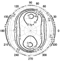
- FIG. 3 is a diagram showing a simulation result of the first implementation model.
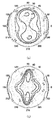
- FIG. 4A is a diagram showing a simulation result of the second implementation model, and
- FIG. 4B is a diagram showing a simulation result of the third implementation model.
- FIG. 5A is a diagram showing a simulation result of the fourth implementation model, and
- FIG. 5B is a diagram showing a simulation result of the fifth implementation model.
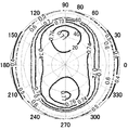
- FIG. 6 is a diagram showing a simulation result of the comparative model.
- the angle dependency of the transmitted light intensity is small, and the result that the polarization reuse efficiency is high can be obtained.
- the optical axis 51 of the crystal substrate 11 is within an angle of rise of ⁇ 15 ° from the substrate surface, and the azimuth angle ⁇ i is 45 ° ⁇ from the transmission axis 50 of the polarizer 10. It was confirmed that when the angle was within 10 ° or within ⁇ 45 ° ⁇ 10 °, the angle dependency was relatively small, and the polarization reuse efficiency was high. From FIG. 5A and FIG. 5B, if the phase difference ⁇ is within 90 ° ⁇ 20 ° and the phase difference order m is 2 or less, the angle dependence is relatively small and high polarization reuse efficiency.
- the phase difference ⁇ is within 90 ° ⁇ 20 ° and the phase difference order m is 2 or less
- FIG. 6 shows that when the phase difference order is 10, the angle dependency is particularly large when the azimuth angle ⁇ i is 45 °, 135 °, 225 °, and 315 °. As a result, the polarization reuse efficiency decreases.
- the heat dissipation effect of the polarizer can be enhanced by using the crystal substrate that has a small angle dependency of the change in the polarization state, so that the polarized light can be reused efficiently. It becomes like this. More specifically, the transmitted light can be linearly polarized light in a specific direction and the reflected light can be circularly polarized light, and their angular dependence can be suppressed.
- a polarizing element 2 ⁇ / b> B may be provided in which a second crystal substrate 14 is additionally provided and the crystal substrate 11 is sandwiched between the second crystal substrate 14 and the polarizer 10.
- the polarizer 10 and the crystal substrate 11 and the crystal substrate 11 and the second crystal substrate 14 are arranged in close contact with each other.
- the transmitted polarized light is linearly polarized light in a specific direction, and the reflected polarized light is circularly polarized light. In this state, the heat dissipation effect can be further enhanced.
- the phase difference of the crystal substrate 11 can be changed as appropriate according to the application.
- FIG. 8 is a perspective view of the polarizing element 2C according to the present embodiment.
- An optical compensation medium 12 is additionally provided in the polarizing element 2C with respect to the polarizing element 2A according to the first embodiment.
- the optical compensation medium 12 and the polarizer 10 sandwich the crystal substrate 11.
- the optical compensation medium 12 is an anisotropic medium in which the optical axis 52 is substantially parallel to the optical axis 51 of the crystal substrate 11.
- Examples of the material of the optical compensation medium 12 include a polarizing element having a fine structure such as a crystal such as crystal or sapphire, an anisotropic film such as polycarbonate, or a photonic crystal.
- the optical axis 52 is a direction substantially parallel to the optical axis 51 of the crystal substrate 11.
- the difference from the optical axis 51 is a polar angle ⁇ i within 15 ° and an azimuth angle ⁇ i within 10 °. More preferably, the polar angle ⁇ i is within 5 ° and the azimuth angle ⁇ i is within 3 °.
- the refractive index of the crystal substrate 11 and the refractive index of the optical compensation medium 12 (long-axis direction refractive index n c // , short-axis direction refractive index n c ⁇ of the refractive index ellipsoid ) satisfy the following relationship: Is preferred.
- the refractive index anisotropy of the crystal substrate 11 is positive ( ns // > n s ⁇ )
- the refractive index anisotropy of the optical compensation medium 12 is negative (nc // ⁇ nc )).
- the refractive index anisotropy of the optical compensation medium 12 is positive (nc // > nc ⁇ ).
- the refractive index anisotropy of sapphire is negative, and the refractive index anisotropy of quartz is positive.
- the thickness d c of the optical compensation medium 12 Given in.
- k is a positive integer.
- the thickness d c of the optical compensation medium 12 shown in this Equation 2 the polarization state of light transmitted through the crystal substrate 11 and the optical compensation substrate 12, a thickness approximately the same even change the incident angle.
- the actual thickness of the optical compensation medium 12 within ⁇ 10% of the thickness d c given by equation 2. More preferably, it is within ⁇ 3%.
- k is To a value within ⁇ 2 from the integer closest to k ′ obtained from More preferably, it is the nearest integer. Further, the difference between the optical axis of the optical compensation medium 12 and the optical axis 51 of the crystal substrate 11 is within 10 °.
- the direction of light incident on the polarizing element 2C is from the optical compensation substrate 12 side.
- FIG. 9 is a principle diagram showing changes in the polarization state of light in the crystal substrate 11 and the optical compensation medium 12.
- the refractive index anisotropy of the crystal substrate 11 is positive and the refractive index anisotropy of the optical compensation medium 12 is negative, or the crystal substrate 11 the refractive index anisotropy negative, and, by the refractive index anisotropy of the optical compensation medium 12 is positive, it is possible to make the delta 90 to delta.
- the thickness d c of the optical compensation medium 12, by the value of the formula 2 and 3, can be further closer to the delta 90 delta.
- Example 2 Next, examples will be described. In this example, a simulation related to the polarization state was performed using a first implementation model described later.
- the polarizing element of the first implementation model is a multilayer film reflective polarizer having a transmission axis orientation of 90 ° as the polarizer 10, and the crystal substrate 11 has an optic axis in the xy plane and an azimuth angle ⁇ i of 45.
- the light source was arranged on the optical compensation medium 12 side, and one light was incident on all angles with random polarization.
- the reflectance of the light source was 0.6, and regular reflection with the polarization state preserved was assumed.
- FIG. 10 shows a simulation result of the angle dependence of the transmittance in the transmission polarization direction of the polarizer 10 of the first implementation model.
- the simulation result shown in FIG. 10 is almost the same as the simulation result shown in FIG. 3, and the angle dependency of the transmitted light intensity is small, indicating that the polarization reuse efficiency is high.
- the polarizing element of this configuration it is possible to enhance the heat dissipation effect of the polarizing element by using a crystal substrate having a small angle dependency of the change in the polarization state, and it is possible to efficiently reuse the polarized light.
- the use of the optical compensation medium makes it possible to increase the thickness of the crystal substrate, thereby improving the ease of processing and the ease of handling.
- the present embodiment is not limited to this.
- a polarizing element 2D configured as shown in FIG. 11 is possible.
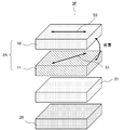
- a second crystal substrate 14 is additionally provided with respect to the polarizing element 2C.
- the polarizer 10 is disposed in close contact between the crystal substrate 11 and the second crystal substrate 14, and the optical compensation medium 12 is disposed on the crystal substrate 11 side.
- the optical axis 54 of the second crystal substrate 14 substantially parallel or substantially orthogonal to the transmission axis 50 of the polarizer 10 or substantially in the thickness direction, the heat dissipation effect can be further enhanced.
- the optical compensation medium 12 may be configured by combining a plurality of anisotropic media.
- FIG. 12 is a perspective view of the optical device 3A including the polarizing element described above.
- the various polarizing elements 2A to 2D described above can be used as the polarizing element, but in the following description, the case where the polarizing element 2A is used will be described as an example.
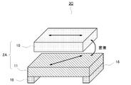
- the optical device 3A includes a cooling fan 15 that cools the polarizing element 2A.
- the cooling fan 15 blows air toward the crystal substrate 11 and the polarizer 10. Therefore, the heat of the crystal substrate 11 and the polarizer 10 can be efficiently dissipated.
- the heat dissipation effect of the polarizer can be enhanced by using a crystal substrate that has a small angle dependency of the change in the polarization state, so that the polarized light can be reused efficiently. become.
- the optical device according to the present embodiment is provided with a heat sink that promotes heat dissipation of the crystal substrate.
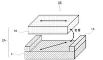
- FIG. 13 is a perspective view of an optical device 3B including the polarizing element described above.
- the various polarizing elements 2A to 2D described above can be used as the polarizing element, but in the following description, the polarizing element 2A will be described as an example.
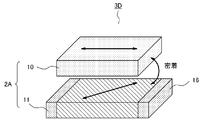
- the optical device 3B has a configuration in which a heat sink 16 is provided on the surface of the crystal substrate 11 on the polarizer 10 side. Note that this embodiment does not limit the manner of attachment when the heat sink 16 is attached to the crystal substrate 11. Therefore, a heat sink 16 may be provided on the surface of the crystal substrate 11 opposite to the polarizer 10 as shown in FIG. 14, or a heat sink may be provided on the end surface of the crystal substrate 11 as shown in FIG. However, the heat sink 16 needs to be attached in close contact with the crystal substrate 11 so as not to hinder the heat conduction of the crystal substrate 11. A heat conductive sheet or a heat conductive gel may be sandwiched between the metal and the crystal substrate.
- Such a heat sink 16 may be a metal material having high thermal conductivity such as aluminum or copper. Thus, by providing the heat sink, the heat of the crystal substrate can be efficiently dissipated.
- the heat dissipation effect of the polarizer can be enhanced by using the crystal substrate having a small angle dependency of the change in the polarization state, and the polarized light can be reused efficiently.
- the optical device according to the present embodiment includes the polarizing element and the light source described above.
- FIG. 16 is a perspective view of the optical device 3E according to the present embodiment.
- the various polarizing elements 2A to 2D described above can be used as the polarizing element, but in the following description, the polarizing element 2A will be described as an example.
- Examples of the light source 20 include a semiconductor light emitting device (LED), a cold cathode tube, an organic EL, an inorganic EL, a high pressure mercury lamp, and a metal halide lamp. At this time, it is possible to include a light guide for guiding light to the polarizing element in the light source.
- LED semiconductor light emitting device
- a cold cathode tube an organic EL
- an inorganic EL an inorganic EL
- a high pressure mercury lamp and a metal halide lamp.
- the light emitted from the light source 20 is randomly polarized light and visible light in the present embodiment.
- the polarizing element 2A transmits only specific polarized light and reflects other light.
- the light reflected by the polarizing element 2A is reflected by the light source 20 and enters the polarizing element 2A again. Therefore, only specific polarized light can be extracted while effectively using the light emitted from the light source 20.
- the optical device 3E a configuration in which the light source 20 and the polarizing element 2A are all closely attached is preferable. By setting it as such a structure, the frequency
- the present embodiment is not limited to the configuration described above.
- the light source device 3F shown in FIG. 17 and the light source device 3G shown in FIG. 18 are possible.
- the optical element 21 is disposed between the light source 20 and the polarizing element 2A.
- This optical element 21 is a dielectric multilayer film angle control filter that transmits only light incident in a specific incident angle range and reflects other light, a diffusion element that diffuses light while maintaining a polarization state, or A combination of these is possible.
- the angle of light is controlled by the optical element 21. Therefore, specific polarized light can be extracted more efficiently while reusing polarized light.
- the optical element 21 mentioned above is the structure arrange
- a light guide 22 is disposed between the light source 20 and the polarizing element 2A.
- the light guide section 22 is formed in a tapered shape, and makes illumination light having a larger area and higher directivity incident on the polarizing element 2A from light having a smaller area and lower directivity.
- the light guide unit 22 in close contact with the polarizing element 2A and the light source 20, since the number of surface reflections can be reduced.
- the light guide part 22 does not need to have a taper shape.
- the optical element 21 may be disposed between the light source 20 and the light guide unit 22 or between the light guide unit 22 and the crystal substrate 11.
- the light source 20, the light guide unit 22, and the polarizing element 2A are arranged in this order.
- the light source 20, the polarizing element 2A, and the light guide unit 22 may be arranged in this order.
- the optical compensation medium 12 may be disposed between the light source 20 and the polarizing element 2A.
- the optical element 21 may be disposed between the light source 20 and the light guide unit 22 or between the light guide unit 22 and the polarizing element 2A.
- the polarizing element 2A is composed of the polarizer 10 and the crystal substrate 11, the second crystal substrate, the polarizer 10, and the crystal substrate 11 are sequentially formed using the second crystal substrate described above. It may be laminated.
- the optical axis 52 of the second crystal substrate 14 is configured to be substantially parallel or substantially orthogonal to the transmission axis 50 of the polarizer 10 or substantially in the thickness direction.
- the video display device includes the optical device described above.
- the optical device 3E will be described as an example of the optical device, but the present invention is not limited to this.
- FIG. 19 is a cross-sectional view of the video display device 4A according to the present embodiment.
- the video display device 4A has a configuration in which an optical device 3E, a liquid crystal cell 33, and a polarizer 34 are arranged in this order.
- the polarizer 34 is an absorption polarizer made by adsorbing and orienting iodine compound molecules mainly composed of polyvinyl alcohol, an organic multilayer reflective polarizer in which an isotropic film and an anisotropic film are laminated in multiple layers, It is possible to use a wire grid polarizer in which metals are arranged in a grid, a photonic crystal polarizer having a photonic structure formed of an inorganic multilayer film, or the like.
- the polarizing element 2A emits the incident light to the liquid crystal cell 33 as linearly polarized light having only a component in the transmission axis direction of the polarizer 10.
- the liquid crystal cell 33 is a spatial light modulator that modulates the phase of incident polarized light in accordance with an input video signal and changes the polarization state.
- the light emitted from the liquid crystal cell 33 enters the polarizer 34, and this polarizer 34 emits only the component in the transmission axis direction of the polarizer 34 of the incident polarized light. As a result, an image corresponding to the image signal can be displayed.
- another polarizing element may be disposed between the polarizing element 2A and the liquid crystal cell 33.
- FIG. 20 is a schematic configuration diagram of a video display device (projector) 4B according to the present embodiment.
- This video display device 4B includes light sources 20R, 20G, and 20B, illumination optical systems 42R, 42G, and 42B, an optical device 3E, liquid crystal cells 33R, 33G, and 33B, a cross dichroic prism 43, and a projection optical system 44. Is provided.
- the light sources 20R, 20G, and 20B generate light having different wavelengths.
- red (R) light is emitted from the light source 20R
- green (G) light is emitted from the light source 20G
- blue (B) light is emitted from the light source 20B.
- the illumination optical systems 42R, 42G, and 42B guide each color light generated from the light sources 20R, 20G, and 20B to the polarization element 2A and make it incident.
- the linearly polarized light of each color transmitted through the polarizing element 2A enters the liquid crystal cells 33R, 33G, and 33B.
- the liquid crystal cells 33R, 33G, and 33B are spatial light modulation elements that modulate incident color light according to a video signal and emit the modulated light.
- the light transmitted through the liquid crystal cells 33R, 33G, and 33B is modulated by the polarizer.
- the cross dichroic prism 43 combines and outputs the modulated lights from the polarizing element 2A.
- the projection optical system 44 projects the combined light emitted from the cross dichroic prism 43 onto the screen S and displays an image corresponding to the video signal on the screen S.
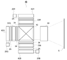
- FIG. 21 is a layout diagram showing another example of the configuration of the video display device (projector) of the present embodiment.
- the video display device 4 ⁇ / b> C includes light sources 20 ⁇ / b> R, 20 ⁇ / b> G, and 20 ⁇ / b> B, a polarizing element 2 ⁇ / b> A, a liquid crystal panel 35, a polarizer 34, an illumination optical system 45, and a projection optical system 46.
- the polarizing element 2A may be any of the polarizing elements 2B to 2D and the optical devices 3A, 3B, 3C, and 3D.
- the liquid crystal panel 35 in this embodiment, it is assumed that the video display device 4A in the sixth embodiment is used.
- the illumination optical system 45 synthesize
- the linearly polarized light transmitted through the polarizing element 2 ⁇ / b> A is incident on the liquid crystal cell 33.
- the liquid crystal cell 33 is a spatial light modulation element that modulates incident combined light according to a video signal and emits the modulated light. After passing through the liquid crystal cell, the polarizer 34 transmits only light in a specific polarization direction among the modulated light.
- the projection optical system 45 projects the modulated light emitted from the polarizer 34 onto the screen S and displays an image corresponding to the video signal on the screen S.
- the video projection apparatus described above it is possible to suppress a decrease in contrast, a decrease in luminance, and a color shift of the video display apparatus while improving the heat dissipation effect of the polarizing element.
- a polarizing element suitably also in positions other than before and after the incidence of a liquid crystal cell.
- a polarizing element can be disposed between the light source and the illumination optical system, or in the illumination optical system, between the light source and the illumination optical system, or in the illumination optical system.
- ⁇ Appendix 1> A polarizer, A crystal substrate disposed in close contact with the polarizer, The crystal substrate has an optical axis whose rising angle from the substrate surface is within ⁇ 15 ° and whose azimuth angle ⁇ i is within 45 ° ⁇ 10 ° or ⁇ 45 ° ⁇ 10 ° from the polarizer transmission axis.
- ⁇ Appendix 6> Appendices 1 to 5, wherein a second crystal substrate is provided so as to be in close contact with the surface of the polarizer opposite to the crystal substrate and sandwich the polarizing element with the crystal substrate.
- the polarizing element described in any one of ⁇ Appendix 7> The polarizing element according to appendix 6, wherein the optical axis of the second crystal substrate is substantially parallel to the polarizer transmission axis, substantially orthogonal to the polarizer transmission axis, or substantially equal to the thickness direction.
- an optical compensation medium is provided that sandwiches the crystal substrate with the polarizer,
- ⁇ Appendix 10> The polarizing element according to appendix 8 or 9, wherein the sign of the refractive index anisotropy of the crystal substrate is opposite to the sign of the anisotropy of the refractive index of the optical compensation medium ⁇ Appendix 11> 11.
- the polarizing element according to any one of appendices 8 to 10 wherein the refractive index anisotropy of the crystal substrate is negative and the refractive index anisotropy of the optical compensation medium is positive.
- the thickness of the optical compensation medium is set to a thickness at which the polarization state of the transmitted light when the incident angle is changed is the same as the polarization state of the incident light.
- the thickness d c of the optical compensation medium is such that the refractive index in the major axis direction of the crystal substrate is n s // , the refractive index in the minor axis direction is n s ⁇ , and the thickness is d s.
- an integer k is used, 14.
- the polarizing element according to appendix 13 wherein the thickness of the optical compensation medium is set to a value in a range of ⁇ 10% of the value obtained in (1).
- ⁇ Appendix 15> The integer k is The polarizing element according to appendix 14, wherein the polarizing element is a value within ⁇ 2 from an integer closest to k ′ represented by: ⁇ Appendix 16> While comprising the polarizing element according to any one of appendices 1 to 15,
- An optical device comprising at least one of a cooling fan that sends air to the polarizing element, a heat sink provided in close contact with the crystal substrate of the polarizing element, and a light source that emits light toward the polarizing element. apparatus.
- ⁇ Appendix 17> The optical apparatus according to appendix 16, wherein an optical element is provided between the light source and the polarizing element.
- ⁇ Appendix 18> The optical element transmits only light incident in a specific incident angle range and reflects other light, a diffusion element that diffuses light while maintaining the polarization state, or a combination of these 18.
- the optical device according to appendix 17, wherein ⁇ Appendix 19> The polarizing element according to any one of appendices 1 to 15, A video display device comprising: a modulation element that modulates light according to a video signal and emits the light.
- a video display device comprising: ⁇ Appendix 22> The optical device according to any one of appendices 16 to 18, An illumination optical system in which light emitted from the light source enters and enters the modulation element; A modulation element that modulates light according to a video signal; A projection optical system that projects light from the modulation element onto a screen;
- a video display device comprising: ⁇ Appendix 23> The video display device according to any one of appendices 19 to 22, wherein the modulation
- Polarizing element 3A to 3G
- 4A to 4C Video display device 10
- Polarizer 11 Crystal substrate 12, 13
- Optical compensation medium 14
- Crystal substrate 15
- Cooling fan 16
- Light source 21 Optical element 22
- Polarizer 35
- Illumination optical system 43
Landscapes
- Physics & Mathematics (AREA)
- General Physics & Mathematics (AREA)
- Optics & Photonics (AREA)
- Polarising Elements (AREA)
- Liquid Crystal (AREA)
- Projection Apparatus (AREA)
Description
本発明は、光の偏光状態を変換する偏光素子、光学装置及び映像表示装置に関する。
プロジェクタは、光源と、光源からの出射光が入射される照明光学系と、照明光学系からの光を映像信号に応じて変調して出射する変調素子と、変調素子からの光をスクリーンに投射する投射光学系とを備えている。このようなプロジェクタでは、変調素子として液晶パネル等の偏光依存性を有する素子が使用されることがある。
液晶パネルは、液晶セルと、その前後に配置された偏光子とを備えている。液晶セルの前に配置された偏光子は、光源から出射した光を特定の偏光状態に変換し、液晶セルは入射した光の偏光状態を別の偏光状態に変換する。そして、液晶セルの後に配置した偏光子は、液晶セルを透過した光のうち、特定の偏光のみを透過させる。
偏光子としては、透過軸方向以外の方向の偏光を吸収する吸収型偏光子や透過軸方向以外の方向の偏光を反射する反射型偏光子が挙げられる。いずれの素子においても、透過軸方向に振動する直線偏光が出射される。
特許文献1には、反射型偏光子を用いて反射される偏光を再利用し、液晶表示体の輝度を向上させる方法が提案されている。
反射型偏光子であるグリッド偏光子を利用して、透過光はそのまま液晶パネルに入射させ、反射光は4分の1波長板を前面に配置したミラーで反射させる。これにより、偏光面を90°回転させて偏光子を通過させ、液晶パネルに入射させる。この結果、偏光子での光の損失が減少し、画面の輝度が向上する。
ここで、偏光子は、わずかでも光の吸収が生じると発熱する。発熱により偏光子の温度が上昇すると、透過方向透過率の低下、吸収(または反射)方向透過率の上昇、ヘイズの上昇といった偏光子の特性劣化が生じる。偏光子の特性劣化は、プロジェクタのコントラスト低下や輝度低下、色ずれを引き起こす要因となる。そこで、偏光子の放熱効果を高めるために、熱伝導率の高い水晶基板やサファイア基板といった結晶基板を冷却板として密着させる提案がなされている(特許文献2、3)。
このような各特許文献に開示された技術に基づき、4分の1波長板として機能する結晶基板と、反射型偏光子とを組み合わせて形成し、結晶基板に冷却板と4分の1波長板の両機能を持たせる構成が考えられる。
しかしながら、水晶基板やサファイア基板は、1つの光学軸を有する一軸性結晶基板であるため、以下のような問題があった。即ち、結晶基板の位相差には入射角依存性があることから、光の入射角によって、位相差が90°(4分の1波長)と異なる値になる。この結果、光の入射角によっては、偏光再利用効率が極端に低下してしまう問題が生じる。例えば、結晶基板の位相差が180°のとき、結晶基板を2度通過すると、偏光が180°回転し、元の偏光に戻ってしまうことから、反射した偏光を再利用することができない。
このように反射型偏光子と4分の1波長板とを組み合わせて偏光再利用を行う構成においては、偏光子の放熱効果を向上し、また偏光再利用効率の角度依存性の抑制を同時に行う技術が求められている。
そこで、本発明の主目的は、結晶基板を用いて偏光子の放熱効果を向上させると共に、偏光再利用効率の角度依存性が抑制できる偏光素子、光学装置及び映像表示装置を提供することである。
上記の課題を解決するために、偏光素子は、直線偏光を透過させ、それ以外の偏光を反射する偏光子と、前記偏光子に密着して配置された結晶基板と、を備え、前記結晶基板は、光学軸が、基板面からの起き上がり角が±15°以内、方位角φiが前記偏光子透過軸から45°±10°以内または-45°±10°以内であり、位相差が、整数の位相差次数mを用いて、(90°+180°×m)±20°以内であり、位相差次数mが2以下の一軸性結晶基板であることを特徴とする。
また、光学装置は、上記偏光素子を備えると共に、前記偏光素子に送風を送る冷却ファン、前記偏光素子の前記結晶基板に密着して設けられたヒートシンク、前記偏光素子に向けて光を出射する光源の少なくとも1つを備えたことを特徴とする。
さらに、映像表示装置は、上記光学装置と、入射光の偏光状態を変える液晶セルと、備えることを特徴とする。
本発明によれば、結晶基板を用いて、偏光子の放熱効果を高めつつ、偏光子の透過前後での偏光状態の変化の角度依存性を抑えた偏光素子を提供することができる。
(第1の実施形態)
本発明の第1の実施形態を説明する。図1は、本実施形態にかかる偏光素子2Aの斜視図である。この偏光素子2Aは、偏光子10と、偏光子10に密着して配置された結晶基板11とから構成されている。以下の説明では、偏光素子2Aに入射する光は、結晶基板11側から入射させるとする。
本発明の第1の実施形態を説明する。図1は、本実施形態にかかる偏光素子2Aの斜視図である。この偏光素子2Aは、偏光子10と、偏光子10に密着して配置された結晶基板11とから構成されている。以下の説明では、偏光素子2Aに入射する光は、結晶基板11側から入射させるとする。
図2は、光の進行方向Dをxyz座標において入射角度(方位角φiと極角θi)を用いて定義した図である。
偏光子10は、特に反射型偏光子である。このような偏光子10として、例えば等方性フィルムと異方性フィルムとを多層積層させた多層フィルム反射型偏光子、金属をグリッド状に配置したワイヤグリッド偏光子、無機の多層膜で形成されたフォトニック構造を有するフォトニック結晶偏光子等が挙げられる。
結晶基板11は、一軸性結晶基板である。そして、この結晶基板11の光学軸51は、基板面からの起き上がり角が±15°以内、方位角φiは偏光子透過軸50から45°±10°以内または-45°±10°以内である。また、位相差は、整数の位相差次数mを用いて、(90°+180°×m)±20°以内である。ここで、位相差次数mは2以下の正の整数である。
結晶基板11の熱伝導率は、5W/(m・K)以上が好ましい。また、可視光波長領域で透明なものが好ましい。このような結晶基板11として、例えば水晶やサファイアが挙げられる。結晶基板11の光学軸51は、基板面からの起き上がり角が±15°以内、方位角φiが偏光子透過軸50から45°±10°以内または-45°±10°以内とする。より好ましくは、基板面からの起き上がり角が±5°以内、方位角φiが偏光子透過軸50から45°±3°以内または-45°±10°以内である。位相差Δは、mを正の整数として、(90°+180°×m)±20°以内である。より好ましくは、(90°+180°×m)±5°以内である。ここで、mは位相差次数であり、2以下である。より好ましくは、位相差次数mは、0である。
次に、このような構成の偏光素子2Aの動作を説明する。このとき、結晶基板11や偏光子10の面は、xy面内であり、これらの厚み方向はz軸方向とする。方位角φiは、光の進行方向Dをxy面内に投影した際の投影写像がx軸とのなす角である。極角θiは、光の進行方向Dとz軸とのなす角である。以下、偏光子10の透過軸50は、y軸方向に平行とする。
また、光源からの光はランダム偏光であり、光源、結晶基板11及び偏光子10で回折や拡散は生じないとする。そして、結晶基板11は、入射した光をそのまま(入射光がランダム偏光であればランダム偏光のまま)出射する。
偏光子10は、透過軸50の方向の直線偏光を透過させるが、それ以外の方向の偏光は反射する。反射された光は、結晶基板11に入射する。結晶基板11に入射した反射光は、結晶基板11の位相差Δsにより偏光状態が変化して、出射する。光の波長がλのとき、結晶基板11の屈折率楕円体の長軸方向屈折率をns//、短軸方向屈折率をns⊥、厚みをdsとすると、
 に示す位相差Δsが生じる。
光学軸51がずれると、位相差Δsが式1で表される値から変化する。位相差の変化について検討したところ、光学軸51は、基板面からの起き上がり角が±15°以内、方位角φiが偏光子10の透過軸50から45°±10°以内または-45°±10°以内であれば、その影響は小さいことがわかった。より好ましくは、基板面からの起き上がり角が±5°以内、方位角φiが偏光子10の透過軸50から45°±3°以内である。
位相差Δsは、(90°+180°×m)に等しいとき、光源と反射型偏光子10とを組み合わせた光源ユニットにおいて、最も効率的に偏光を再利用することができる。そして、(90°+180°×m)からの差が20°以内であれば、位相差のずれによる影響は小さい。より好ましくは5°以内である。
ここで、式1から次数mが大きくなる(即ち、厚みdsが大きくなる)につれて、位相差Δsの入射極角θi依存性が大きくなることがわかる。この入射極角θi依存性を低減させるためには、次数mは2以下が好ましい。より好ましい位相差次数mは0である。
(実施例)
次に、実施例を説明する。本実施例では、後述する第1実施モデル~第5実施モデル、比較モデルの偏光素子を用いて、その偏光状態に関するシミュレーションを行った。
次に、実施例を説明する。本実施例では、後述する第1実施モデル~第5実施モデル、比較モデルの偏光素子を用いて、その偏光状態に関するシミュレーションを行った。
<第1実施モデル> 第1実施モデルの偏光素子は、偏光子10として透過軸方位角φiが90°の多層フィルム反射型偏光子、結晶基板11として光学軸が極角θiが90°、方位角φiが45°のサファイア基板(屈折率:ns//=1.7637,ns⊥=1.7718、厚み:ds=16.3μm(次数0))を用いた。
<第2実施モデル> 第2実施モデルの偏光素子は、偏光子10として透過軸方位角φiが90°の多層フィルム反射型偏光子、結晶基板11として光学軸が極角θiが75°、方位角φiが45°のサファイア基板(屈折率:ns//=1.7637,ns⊥=1.7718、厚み:ds=16.3μm「次数0」)を用いた。
<第3実施モデル> 第3実施モデルの偏光素子は、偏光子10として透過軸方位角φiが90°の多層フィルム反射型偏光子、結晶基板11として、光学軸が極角θiが90°、方位角φiが35°のサファイア基板(屈折率:ns//=1.7637,ns⊥=1.7718、厚み:ds=16.3μm「次数0」)を用いた。
<第4実施モデル> 第4実施モデルの偏光素子は、偏光子10として透過軸方位角φiが90°の多層フィルム反射型偏光子、結晶基板11として光学軸が極角θiが90°、方位角φiが45°のサファイア基板(屈折率:ns//=1.7637,ns⊥=1.7718、厚み:ds=12.6μm「位相差70°」)を用いた。
<第5実施モデル> 第5実施モデルの偏光素子は、偏光子10として透過軸方位角φiが90°の多層フィルム反射型偏光子、結晶基板11として光学軸が極角θiが90°、方位角φiが45°の水晶基板(屈折率:ns//=1.5562,ns⊥=1.5470、厚み:ds=71.9μm「次数2」)を用いた。
<比較モデル> 比較モデルの偏光素子は、偏光子10として透過軸方位が90°の多層フィルム反射型偏光子、結晶基板11として光学軸が極角θiが90°、方位角φiが45°のサファイア基板(屈折率:ns//=1.7637,ns⊥=1.7718、厚み:ds=341.5μm「次数10」)を用いた。
これらの偏光素子に対して、光源は結晶基板11側に配置され、その出射光はランダム偏光とした。なお、光源の反射率は0.6で、偏光状態が保存される正反射であるとした。そして、偏光子10の透過偏光方向の透過率の角度依存性をシミュレーションした。
図3は、第1実施モデルのシミュレーション結果を示した図である。図4(a)は、第2実施モデルのシミュレーション結果を示す図、図4(b)は第3実施モデルのシミュレーション結果を示す図である。また、図5(a)は第4実施モデルのシミュレーション結果を示す図、図5(b)は第5実施モデルのシミュレーション結果を示す図である。さらに、図6は、比較モデルのシミュレーション結果を示す図である。
図3から、第1実施モデルの偏光素子では、透過光強度の角度依存性が小さく、偏光再利用効率が高い結果を得ることができた。また、図4(a)及び図4(b)から、結晶基板11の光学軸51が基板面からの起き上がり角±15°以内、方位角φiが偏光子10の透過軸50から45°±10°以内または-45°±10°以内であれば、角度依存性が比較的小さく、偏光再利用効率が高い結果を得ることが確認できた。図5(a)及び図5(b)から、位相差Δが90°±20°以内であり、位相差次数mが2以下であれば、角度依存性は比較的小さく、高い偏光再利用効率を得ることが確認できた。
また、図6から、位相差次数が10のとき、特に方位角φiが45°、135°、225°、315°での角度依存性が大きいことが示された。この結果、偏光再利用効率が低下する。
以上から、本構成の偏光素子によれば、偏光状態の変化の角度依存性が小さい結晶基板を用いて偏光子の放熱効果を高めることができるので、偏光を効率的に再利用することができるようになる。具体的には、透過偏光を特定方向の直線偏光、反射偏光を円偏光とし、それらの角度依存性を抑えることができる。
なお、本構成の偏光素子2Aでは、偏光子10の片面のみに結晶基板11を密着配置する構成を示したが、本実施形態は、これに限定されない。例えば、図7に示すように、第2の結晶基板14を追設して、この第2の結晶基板14と偏光子10とで結晶基板11を挟むように設けた偏光素子2Bでも良い。この場合、偏光子10と結晶基板11、結晶基板11と第2の結晶基板14は、それぞれ密着して配置する。
第2の結晶基板14の光学軸54を偏光子10の透過軸50とほぼ平行又はほぼ直交、或はほぼ厚み方向とすることで、透過偏光を特定方向の直線偏光、反射偏光を円偏光とした状態で、放熱効果をさらに高めることができる。なお、結晶基板11の位相差は、用途に合わせて適宜変更することができる。
(第2の実施形態)
次に、本発明の第2の実施形態を説明する。なお、第1の実施形態と同一構成に関しては同一符号を用いて説明を適宜省略する。
次に、本発明の第2の実施形態を説明する。なお、第1の実施形態と同一構成に関しては同一符号を用いて説明を適宜省略する。
図8は、本実施形態にかかる偏光素子2Cの斜視図である。偏光素子2Cには、第1の実施形態にかかる偏光素子2Aに対して光学補償媒体12が追設されている。そして、この光学補償媒体12と偏光子10とで結晶基板11を挟んでいる。光学補償媒体12は、光学軸52が結晶基板11の光学軸51とほぼ平行な異方性媒体である。
光学補償媒体12の材料は、例えば水晶やサファイア等の結晶やポリカーボネートのような異方性フィルム、フォトニック結晶といった微細構造の偏光素子が挙げられる。
光学軸52は、結晶基板11の光学軸51とほぼ平行な方向であり、例えば光学軸51からの差が極角θiが15°以内、方位角φiが10°以内である。より好ましくは、極角θiが5°以内、方位角φiが3°以内である。
特に、結晶基板11の屈折率と光学補償媒体12の屈折率(屈折率楕円体の長軸方向屈折率nc//、短軸方向屈折率nc⊥)とは、以下の関係を満たすことが好ましい。
即ち、結晶基板11の屈折率異方性が正(ns//>ns⊥)のときは、光学補償媒体12の屈折率異方性が負(nc//<nc⊥)であること、又は結晶基板11の屈折率異方性が負(ns//<ns⊥)のときは、光学補償媒体12の屈折率異方性が正(nc//>nc⊥)であることが望まれる。
サファイアの屈折率異方性は負であり、水晶の屈折率異方性は正である。このとき、光学補償媒体12の厚みdcは、
 で与えられる。ここでkは正の整数である。なお、この式2で示される光学補償媒体12の厚みdcは、結晶基板11と光学補償基板12とを透過した光の偏光状態が、入射角度が変わってもほぼ同じになる厚みである。
そこで、実際の光学補償媒体12の厚みは、式2で与えられる厚みdcの±10%以内とする。より好ましくは、±3%以内とする。そして、kは、
 から得られるk'に最も近い整数から±2以内の値とする。より好ましくは、最も近い整数である。また、光学補償媒体12の光学軸と、結晶基板11の光学軸51との差は10°以内とする。
次に、このように構成された偏光素子2Cの動作について説明する。なお、偏光素子2Cに入射する光の方向は、光学補償基板12側からとする。
図9は、結晶基板11と光学補償媒体12とにおける、光の偏光状態の変化を示す原理図である。入射角が小さい低入射角(θ≒0)のときは、光学補償媒体12では位相差Δc0、結晶基板11では位相差Δs0生じる。従って、結晶基板11からは、両者の和Δ0=Δs0+Δc0の位相差の光が出射する。
一方、入射角が大きい考入射角(θ≒90°)のときは、光学補償媒体12では位相差Δc90、結晶基板11では位相差Δs90生じる。従って、結晶基板11からは、両者の和Δ90=Δs90+Δc90の位相差の光が出射する。
そこで、所望の位相差をΔとして、Δ0=Δとなるように光学補償媒体12の厚みdcを定めると、通常位相差Δ90はΔと異なる値となる(Δ90≠Δ)。
しかし、結晶基板11の屈折率と光学補償媒体12の屈折率とについて、結晶基板11の屈折率異方性が正、かつ、光学補償媒体12の屈折率異方性が負、又は、結晶基板11の屈折率異方性が負、かつ、光学補償媒体12の屈折率異方性が正とすることで、Δ90をΔに近づけることができる。また、光学補償媒体12の厚みdcを、式2、3で表される値とすることで、Δ90をΔにさらに近づけることができる。
(実施例)
次に、実施例を説明する。本実施例では、後述する第1実施モデルを用いて、その偏光状態に関するシミュレーションを行った。
次に、実施例を説明する。本実施例では、後述する第1実施モデルを用いて、その偏光状態に関するシミュレーションを行った。
<第1実施モデル> 第1実施モデルの偏光素子は、偏光子10として透過軸方位が90°の多層フィルム反射型偏光子、結晶基板11として光学軸がxy面内で方位角φiが45°のサファイア基板(屈折率:ns//=1.7637,ns⊥=1.7718、厚み:ds=300μm)、水晶製光学補償媒体(屈折率:ns//=1.5562,ns⊥=1.5470、厚み:ds=193.5μm)を用いた。
光源は光学補償媒体12側に配置され、ランダム偏光で全ての角度に1つの光を入射するものとした。また、光源の反射率は0.6で偏光状態が保存される正反射であるとした。
そして、偏光子10の透過偏光方向の透過率の角度依存性をシミュレーションした。
図10は、第1実施モデルの偏光子10の透過偏光方向の透過率の角度依存性のシミュレーション結果を示している。図10に示すシミュレーション結果は、図3に示すシミュレーション結果とほぼ同等で、透過光強度の角度依存性は小さく、偏光再利用効率が高いことを示している。
従って、本構成の偏光素子によれば、偏光状態の変化の角度依存性が小さい結晶基板を用いて偏光素子の放熱効果を高めることができると共に、偏光を効率的に再利用することができる。
また、光学補償媒体を用いることにより結晶基板の厚みを厚くすることが可能になり、加工の容易性や取扱い易さ等が向上する。
なお、上記説明では、偏光子の片面のみに結晶基板を密着配置する構成を示したが、本実施形態はこれに限定するものではない。例えば、図11に示すような構成の偏光素子2Dが可能である。この偏光素子2Dは、偏光素子2Cに対して第2の結晶基板14が追設されている。
そして、結晶基板11と第2の結晶基板14との間には偏光子10が密着して配置され、結晶基板11側に光学補償媒体12が配置された構成である。第2の結晶基板14の光学軸54は、偏光子10の透過軸50とほぼ平行又はほぼ直交、或はほぼ厚み方向にすることで、さらに放熱効果を高めることができる。
また、結晶基板11と光学補償媒体12とを組み合わせたときの位相差は、用途に合わせて適宜変更することができる。なお、光学補償媒体12は複数の異方性媒体を組み合わせた構成としてもよい。
(第3の実施形態)
次に、本発明の第3の実施形態を説明する。なお、上記実施形態と同一構成に関しては同一符号を用いて説明を適宜省略する。
次に、本発明の第3の実施形態を説明する。なお、上記実施形態と同一構成に関しては同一符号を用いて説明を適宜省略する。
図12は、上述した偏光素子を備えた光学装置3Aの斜視図である。なお、偏光素子として上述した各種の偏光素子2A~偏光素子2Dが利用できるが、以下の説明では、偏光素子2Aを利用する場合を例に説明する。
光学装置3Aは、偏光素子2Aを冷却する冷却ファン15を備える。この冷却ファン15は、結晶基板11及び偏光子10に向けて送風する。従って、結晶基板11及び偏光子10の熱を効率よく放散させることが可能になる。
よって、本構成の光学装置によれば、偏光状態の変化の角度依存性が小さい結晶基板を用いて偏光子の放熱効果を高めることができるので、偏光を効率的に再利用することができるようになる。
(第4の実施形態)
次に、本発明の第4の実施形態を説明する。なお、上記実施形態と同一構成に関しては同一符号を用いて説明を適宜省略する。
次に、本発明の第4の実施形態を説明する。なお、上記実施形態と同一構成に関しては同一符号を用いて説明を適宜省略する。
本実施形態にかかる光学装置は、結晶基板の放熱を促進するヒートシンクを設けたものである。
図13は、上述した偏光素子を備えた光学装置3Bの斜視図である。なお、偏光素子として上述した各種の偏光素子2A~偏光素子2Dが利用できるが、以下の説明では、偏光素子2Aを例に説明する。
光学装置3Bは、偏光子10側の結晶基板11面にヒートシンク16が設けられた構成である。なお、本実施形態は、ヒートシンク16を結晶基板11に取付ける際の取付け態様を限定するものではない。従って、図14に示すように、偏光子10と反対側の結晶基板11面にヒートシンク16を設けても良く、また図15に示すように、結晶基板11の端面にヒートシンクを設けても良い。但し、結晶基板11の熱伝導を妨げないように、ヒートシンク16は結晶基板11と密着して取付ける必要がある。金属と結晶基板との間に熱伝導シートもしくは熱伝導ジェルを挟んでも良い。
このようなヒートシンク16として、アルミニウムや銅等の熱伝導率が高い金属材料が挙げられる。このように、ヒートシンクを設けることで、結晶基板の熱の放散が効率よく行えるようになる。
よって、本構成の光学装置によれば、偏光状態の変化の角度依存性が小さい結晶基板を用いて偏光子の放熱効果を高めるとともに、偏光を効率的に再利用することができるようになる。
(第5の実施形態)
次に、本発明の第5の実施形態を説明する。なお、上記実施形態と同一構成に関しては同一符号を用いて説明を適宜省略する。
次に、本発明の第5の実施形態を説明する。なお、上記実施形態と同一構成に関しては同一符号を用いて説明を適宜省略する。
本実施形態にかかる光学装置は、上述した偏光素子と光源とを備える。図16は、本実施形態にかかる光学装置3Eの斜視図である。なお、偏光素子として上述した各種の偏光素子2A~偏光素子2Dが利用できるが、以下の説明では、偏光素子2Aを例に説明する。
光源20として、半導体発光素子(LED)、冷陰極管、有機EL、無機EL、高圧水銀ランプ、メタルハライドランプが例示できる。このとき、光を偏光素子に導くための導光部を光源に含めることは可能である。
この光源20から出射される光は、本実施形態においては、ランダム偏光であり、かつ、可視光であるとする。偏光素子2Aは、特定の偏光のみ透過させ、それ以外の光は反射する。この偏光素子2Aで反射された光は、光源20で反射されて、再度偏光素子2Aに入射する。従って、光源20で発光した光の有効利用を図りながら、特定の偏光のみを取り出すことが可能になる。
光学装置3Eとして、光源20と偏光素子2Aとは、全て密着配置させた構成が好ましい。このような構成とすることで、各要素の表面で生じる反射回数を減らすことができる。従って、効率的に特定の偏光状態の光が取り出せるようになる。
なお、本実施形態は、上述した構成に限定しない。例えば、図17に示す光源装置3Fや図18に示す光源装置3Gが可能である。
図17に示す光源装置3Fは、光源20と偏光素子2Aとの間に光学素子21が配置されている。この光学素子21は、特定の入射角範囲に入射した光のみを透過させ、それ以外の光を反射させる誘電体多層膜角度制御フィルタ、偏光状態を維持したまま光を拡散させる拡散素子、あるいは、これらを組み合わせた構成が可能である。
これにより、光学素子21によって光の角度が制御される。従って、偏光を再利用しながら、より効率的に特定の偏光を取り出すことができる。なお、上述した光学素子21は偏光素子2Aと光源20との間に配置した構成であるが、光学素子21と光源20とで偏光素子2Aを挟むように配置しても良い。
図18に示す光源装置3Gは、光源20と偏光素子2Aとの間に導光部22が配置されている。導光部22は、テーパ状に形成され、面積が小さく、かつ、指向性の低い光から、より面積が大きく、かつ、指向性の高い照明光を偏光素子2Aに入射させる。
このとき、導光部22は、偏光素子2A及び光源20とそれぞれ密着して設けるならば、表面反射の回数を少なくできるので好ましい。なお、導光部22は、テーパ形状を有していなくてもよい。また、光源20と導光部22の間、もしくは導光部22と結晶基板11の間に、光学素子21を配置してもよい。
また、上記説明では、光源20、導光部22、偏光素子2Aの順に配置したが、光源20、偏光素子2A、導光部22の順に配置しても良い。また、光源20と偏光素子2Aとの間に光学補償媒体12を配置してもよい。光源20と、導光部22との間、あるいは導光部22と偏光素子2Aとの間に、光学素子21を配置してもよい。
さらに、上記偏光素子2Aは偏光子10と結晶基板11とにより構成されていたが、先に述べた第2の結晶基板を用いて、第2の結晶基板、偏光子10、結晶基板11が順次積層されていても良い。このとき第2の結晶基板14の光学軸52は、偏光子10の透過軸50とほぼ平行又はほぼ直交、或はほぼ厚み方向とした構成とする。
(第6の実施形態)
次に、本発明の第6の実施形態を説明する。なお、上記実施形態と同一構成に関しては同一符号を用いて説明を適宜省略する。
次に、本発明の第6の実施形態を説明する。なお、上記実施形態と同一構成に関しては同一符号を用いて説明を適宜省略する。
本実施形態にかかる映像表示装置は、上述した光学装置を備える。なお、以下においては、光学装置として光学装置3Eを例に説明するが、これに限定しない。
図19は、本実施形態にかかる映像表示装置4Aの断面図である。映像表示装置4Aは、光学装置3E、液晶セル33、偏光子34が、この順で配置された構成となっている。
偏光子34は、ポリビニルアルコールを主体に、ヨウ素化合物分子を吸着配向させて作られた吸収型偏光子、等方性フィルムと異方性フィルムとを多層積層させた有機多層膜反射型偏光子、金属をグリッド状に配置したワイヤグリッド偏光子、無機の多層膜で形成されたフォトニック構造のフォトニック結晶偏光子等を用いることが可能である。
そして、偏光素子2Aは、入射した光から偏光子10の透過軸方向の成分のみの直線偏光として液晶セル33に出射する。液晶セル33は、入力された映像信号に応じて入射した偏光の位相を変調し、偏光状態を変化させる空間光変調素子である。液晶セル33から出射された光は偏光子34に入射し、この偏光子34は、入射した偏光のうち偏光子34の透過軸方向成分のみを出射する。これにより、映像信号に応じた映像が表示できるようになる。
以上の構成により、放熱効果の高い偏光素子を用いた映像表示装置で表示される映像のコントラスト低下や輝度低下、色ずれが抑制できる。ここで、コントラストを向上させるために、偏光素子2Aと液晶セル33との間に別の偏光素子を配置しても良い。
(第7の実施形態)
次に、本発明の第7の実施形態を説明する。なお、上記実施形態と同一構成に関しては同一符号を用いて説明を適宜省略する。
次に、本発明の第7の実施形態を説明する。なお、上記実施形態と同一構成に関しては同一符号を用いて説明を適宜省略する。
図20は、本実施形態にかかる映像表示装置(プロジェクタ)4Bの概略構成図である。この映像表示装置4Bは、光源20R、20G及び20Bと、照明光学系42R、42G及び42Bと、光学装置3Eと、液晶セル33R、33G及び33Bと、クロスダイクロイックプリズム43と、投射光学系44とを備える。
そして、光源20R、20G及び20Bは、それぞれ異なる波長の光を発生するものとする。以下、光源20Rから赤色(R)光が出射され、光源20Gから緑色(G)光が出射され、光源20Bから青色(B)光が出射されるものとする。
照明光学系42R、42G及び42Bは、光源20R、20G及び20Bから発生した各色光を、偏光素子2Aに導いて入射させる。偏光素子2Aを透過した各色の直線偏光は、液晶セル33R、33G及び33Bに入射する。液晶セル33R、33G、33Bは、入射された各色光を映像信号に応じて変調して出射する空間光変調素子である。液晶セル33R、33G、33Bを透過した光は、偏光子34で変調される。
そして、変調された光のうち特定の偏光方向の光のみが透過する。クロスダイクロイックプリズム43は、偏光素子2Aからのそれぞれの変調光を合成して出射する。投射光学系44は、クロスダイクロイックプリズム43から出射された合成光をスクリーンSに投射して、スクリーンS上に映像信号に応じた映像を表示する。
なお、本実施形態は、上述構成に限定しない。例えば、図21に示すような構成でも良い。
図21は、本実施形態の映像表示装置(プロジェクタ)の構成の別の例を示す配置図である。図21において、映像表示装置4Cは、光源20R、20G及び20Bと、偏光素子2Aと、液晶パネル35と、偏光子34と、照明光学系45と、投射光学系46とを有する。
偏光素子2Aは、偏光素子2B~2D、光学装置3A、3B、3C、3Dのいずれでもよい。なお、液晶パネル35として、本実施形態では第6の実施形態における映像表示装置4Aを用いるとする。
そして、照明光学系45は、光源20R、20G及び20Bから発生した各色光を合成して、偏光素子2Aに出射する。偏光素子2Aを透過した直線偏光は、液晶セル33に入射する。液晶セル33は、入射された合成光を映像信号に応じて変調して出射する空間光変調素子である。液晶セルを透過後、偏光子34で、変調された光のうち特定の偏光方向の光のみ透過する。
投射光学系45は、偏光子34から出射された変調光をスクリーンSに投射して、スクリーンS上に映像信号に応じた映像を表示する。
以上説明した映像投射装置によれば、偏光素子の放熱効果を向上させた上で、映像表示装置のコントラスト低下や、輝度低下、色ずれを抑えることができる。
なお、液晶セルの入射前後以外の位置にも、偏光素子を適宜配置してよい。例えば、光源と照明光学系の間、あるいは照明光学系内、光源と照明光学系の間、あるいは照明光学系内に、偏光素子を配置することができる。
以上説明した各実施形態において、図示した構成は単なる一例であって、本発明はその構成に限定されるものではない。例えば、上記実施の形態における数値、材質等は例示的なものであり、適宜変更して実施することが可能である。 上記実施の形態の一部又は全部は、以下の付記のようにも記載されうるが、以下には限られない。
<付記1>
偏光子と、
前記偏光子に密着して配置された結晶基板と、を備え、
前記結晶基板は、光学軸が、基板面からの起き上がり角が±15°以内、方位角φiが前記偏光子透過軸から45°±10°以内または-45°±10°以内であり、位相差が、整数の位相差次数mを用いて、(90°+180°×m)±20°以内であり、位相差次数mが2以下の一軸性結晶基板であることを特徴とする偏光素子。
<付記2>
前記偏光子が反射型偏光子であることを特徴とする付記1に記載の偏光素子。
<付記3>
前記結晶基板が、5W/(m・K)以上の熱伝導率を有していることを特徴とする付記1又は2に記載の偏光素子。
<付記4>
前記結晶基板が、サファイアであることを特徴とする付記1乃至3のいずれか1項に記載の偏光素子。
<付記5>
前記結晶基板が、水晶であることを特徴とする付記1乃至3のいずれか1項に記載の偏光素子。
<付記6>
前記偏光子の、前記結晶基板の反対側の面に密着して設けられて、前記結晶基板とで当該偏光素子を挟むように第2の結晶基板を設けたことを特徴とする付記1乃至5のいずれか1項に記載の偏光素子
<付記7>
前記第2の結晶基板の光学軸が、前記偏光子透過軸とほぼ平行又は前記偏光子透過軸とほぼ直交、又は厚み方向にほぼ等しいことを特徴とする付記6に記載の偏光素子。
<付記8>
前記結晶基板の、前記偏光子の反対側の面に密着して、前記結晶基板を前記偏光子とで挟む光学補償媒体を設け、
前記光学補償媒体の光学軸が、前記結晶基板の光学軸とほぼ平行であることを特徴とする付記1乃至7のいずれか1項に記載の偏光素子。
<付記9>
前記光学補償媒体の光学軸が、前記結晶基板の光学軸との差が10°以内であることを特徴とする付記8に記載の偏光素子。
<付記10>
前記結晶基板の屈折率異方性の正負符号と、光学補償媒体の屈折率異方性の正負符号とが、逆であることを特徴とする付記8又は9に記載の偏光素子
<付記11>
前記結晶基板の屈折率異方性が正で、前記光学補償媒体の屈折率異方性が負であることを特徴とする付記8乃至10のいずれか1項に記載の偏光素子。
<付記12>
前記結晶基板の屈折率異方性が負で、前記光学補償媒体の屈折率異方性が正であることを特徴とする付記8乃至10のいずれか1項に記載の偏光素子。
<付記13>
前記光学補償媒体の厚みは、入射角度を変えたときの透過光の偏光状態が入射光の偏光状態と同じになる厚みに設定されていることを特徴とする付記8乃至12のいずれか1項に記載の偏光素子。
<付記14>
前記光学補償媒体の厚みdcは、前記結晶基板の長軸方向の屈折率がns//、短軸方向の屈折率がns⊥、厚みがdsであり、前記光学補償媒体の長軸方向の屈折率がnc//、短軸方向の屈折率がnc⊥のとき、整数kを用いて、
 で得られる値の±10%の範囲の値に当該前記光学補償媒体の厚みを設定したことを特徴とする付記13に記載の偏光素子。
<付記15>
前記整数kが、
 で表されるk'に最も近い整数から±2以内の値であることを特徴とする付記14に記載の偏光素子。
<付記16>
付記1乃至15のいずれか1項に記載の偏光素子を備えると共に、
前記偏光素子に送風を送る冷却ファン、前記偏光素子の前記結晶基板に密着して設けられたヒートシンク、前記偏光素子に向けて光を出射する光源の少なくとも1つを備えたことを特徴とする光学装置。
<付記17>
前記光源と前記偏光素子との間に、光学素子を設けたことを特徴とする付記16に記載の光学装置。
<付記18>
前記光学素子が、特定の入射角範囲に入射した光のみを透過させ、それ以外の光を反射させる角度制御フィルタ、偏光状態を維持したまま光を拡散させる拡散素子、あるいは、これらを組み合わせた構成、であることを特徴とする付記17に記載の光学装置。
<付記19>
付記1乃至15のいずれか1項に記載の偏光素子と、
光を映像信号に応じて変調して出射する変調素子と、を備えることを特徴とする映像表示装置。
<付記20>
付記16乃至18のいずれか1項に記載の光学装置と、
光を映像信号に応じて変調して出射する変調素子と、を備えることを特徴とする映像表示装置。
<付記21>
付記1乃至15のいずれか1項に記載の偏光素子と、
光源からの出射光が入射し、変調素子に入射させる照明光学系と、
光を映像信号に応じて変調させる変調素子と、
前記変調素子からの光をスクリーンに投射する投射光学系と、
を備えることを特徴とする映像表示装置。
<付記22>
付記16乃至18のいずれか1項に記載の光学装置と、
光源からの出射光が入射し、変調素子に入射させる照明光学系と、
光を映像信号に応じて変調させる変調素子と、
前記変調素子からの光をスクリーンに投射する投射光学系と、
を備えることを特徴とする映像表示装置。
<付記23>
前記変調素子は、液晶セルであることを特徴とする付記19乃至22のいずれか1項に記載の映像表示装置。
この出願は、2012年8月14日に出願された日本出願特願2012-179830を基礎とする優先権を主張し、その開示の全てをここに取り込む。
<付記1>
偏光子と、
前記偏光子に密着して配置された結晶基板と、を備え、
前記結晶基板は、光学軸が、基板面からの起き上がり角が±15°以内、方位角φiが前記偏光子透過軸から45°±10°以内または-45°±10°以内であり、位相差が、整数の位相差次数mを用いて、(90°+180°×m)±20°以内であり、位相差次数mが2以下の一軸性結晶基板であることを特徴とする偏光素子。
<付記2>
前記偏光子が反射型偏光子であることを特徴とする付記1に記載の偏光素子。
<付記3>
前記結晶基板が、5W/(m・K)以上の熱伝導率を有していることを特徴とする付記1又は2に記載の偏光素子。
<付記4>
前記結晶基板が、サファイアであることを特徴とする付記1乃至3のいずれか1項に記載の偏光素子。
<付記5>
前記結晶基板が、水晶であることを特徴とする付記1乃至3のいずれか1項に記載の偏光素子。
<付記6>
前記偏光子の、前記結晶基板の反対側の面に密着して設けられて、前記結晶基板とで当該偏光素子を挟むように第2の結晶基板を設けたことを特徴とする付記1乃至5のいずれか1項に記載の偏光素子
<付記7>
前記第2の結晶基板の光学軸が、前記偏光子透過軸とほぼ平行又は前記偏光子透過軸とほぼ直交、又は厚み方向にほぼ等しいことを特徴とする付記6に記載の偏光素子。
<付記8>
前記結晶基板の、前記偏光子の反対側の面に密着して、前記結晶基板を前記偏光子とで挟む光学補償媒体を設け、
前記光学補償媒体の光学軸が、前記結晶基板の光学軸とほぼ平行であることを特徴とする付記1乃至7のいずれか1項に記載の偏光素子。
<付記9>
前記光学補償媒体の光学軸が、前記結晶基板の光学軸との差が10°以内であることを特徴とする付記8に記載の偏光素子。
<付記10>
前記結晶基板の屈折率異方性の正負符号と、光学補償媒体の屈折率異方性の正負符号とが、逆であることを特徴とする付記8又は9に記載の偏光素子
<付記11>
前記結晶基板の屈折率異方性が正で、前記光学補償媒体の屈折率異方性が負であることを特徴とする付記8乃至10のいずれか1項に記載の偏光素子。
<付記12>
前記結晶基板の屈折率異方性が負で、前記光学補償媒体の屈折率異方性が正であることを特徴とする付記8乃至10のいずれか1項に記載の偏光素子。
<付記13>
前記光学補償媒体の厚みは、入射角度を変えたときの透過光の偏光状態が入射光の偏光状態と同じになる厚みに設定されていることを特徴とする付記8乃至12のいずれか1項に記載の偏光素子。
<付記14>
前記光学補償媒体の厚みdcは、前記結晶基板の長軸方向の屈折率がns//、短軸方向の屈折率がns⊥、厚みがdsであり、前記光学補償媒体の長軸方向の屈折率がnc//、短軸方向の屈折率がnc⊥のとき、整数kを用いて、
<付記15>
前記整数kが、
<付記16>
付記1乃至15のいずれか1項に記載の偏光素子を備えると共に、
前記偏光素子に送風を送る冷却ファン、前記偏光素子の前記結晶基板に密着して設けられたヒートシンク、前記偏光素子に向けて光を出射する光源の少なくとも1つを備えたことを特徴とする光学装置。
<付記17>
前記光源と前記偏光素子との間に、光学素子を設けたことを特徴とする付記16に記載の光学装置。
<付記18>
前記光学素子が、特定の入射角範囲に入射した光のみを透過させ、それ以外の光を反射させる角度制御フィルタ、偏光状態を維持したまま光を拡散させる拡散素子、あるいは、これらを組み合わせた構成、であることを特徴とする付記17に記載の光学装置。
<付記19>
付記1乃至15のいずれか1項に記載の偏光素子と、
光を映像信号に応じて変調して出射する変調素子と、を備えることを特徴とする映像表示装置。
<付記20>
付記16乃至18のいずれか1項に記載の光学装置と、
光を映像信号に応じて変調して出射する変調素子と、を備えることを特徴とする映像表示装置。
<付記21>
付記1乃至15のいずれか1項に記載の偏光素子と、
光源からの出射光が入射し、変調素子に入射させる照明光学系と、
光を映像信号に応じて変調させる変調素子と、
前記変調素子からの光をスクリーンに投射する投射光学系と、
を備えることを特徴とする映像表示装置。
<付記22>
付記16乃至18のいずれか1項に記載の光学装置と、
光源からの出射光が入射し、変調素子に入射させる照明光学系と、
光を映像信号に応じて変調させる変調素子と、
前記変調素子からの光をスクリーンに投射する投射光学系と、
を備えることを特徴とする映像表示装置。
<付記23>
前記変調素子は、液晶セルであることを特徴とする付記19乃至22のいずれか1項に記載の映像表示装置。
この出願は、2012年8月14日に出願された日本出願特願2012-179830を基礎とする優先権を主張し、その開示の全てをここに取り込む。
2A~2D 偏光素子
3A~3G 光学装置
4A~4C 映像表示装置
10 偏光子
11 結晶基板
12、13 光学補償媒体
14 結晶基板
15 冷却ファン
16 ヒートシンク
20、20R、20G、20B 光源
21 光学素子
22 導光部
33、33R、33G、33B 液晶セル
34 偏光子
35 液晶パネル(液晶表示装置)
42R、42G、42B、45 照明光学系
43 クロスダイクロイックプリズム
44、46 投射光学系
3A~3G 光学装置
4A~4C 映像表示装置
10 偏光子
11 結晶基板
12、13 光学補償媒体
14 結晶基板
15 冷却ファン
16 ヒートシンク
20、20R、20G、20B 光源
21 光学素子
22 導光部
33、33R、33G、33B 液晶セル
34 偏光子
35 液晶パネル(液晶表示装置)
42R、42G、42B、45 照明光学系
43 クロスダイクロイックプリズム
44、46 投射光学系
Claims (10)
- 偏光子と、
前記偏光子に密着して配置された結晶基板と、を備え、
前記結晶基板は、光学軸が、基板面からの起き上がり角が±15°以内、方位角φiが前記偏光子透過軸から45°±10°以内または-45°±10°以内であり、位相差が、整数の位相差次数mを用いて、(90°+180°×m)±20°以内であり、位相差次数mが2以下の一軸性結晶基板であることを特徴とする偏光素子。 - 前記結晶基板の、前記偏光子の反対側に設けられて、前記結晶基板を前記偏光素子とで挟む位置に設けられた光学補償媒体を備え、
前記光学補償媒体の光学軸が、前記結晶基板の光学軸とほぼ平行であることを特徴とする請求項1に記載の偏光素子。 - 前記結晶基板の屈折率異方性の正負符号と、光学補償媒体の屈折率異方性の正負符号とが、逆であることを特徴とする請求項2に記載の偏光素子
- 前記光学補償媒体の厚みは、入射角度を変えたときの透過光の偏光状態が入射光の偏光状態と同じになる厚みに設定されていることを特徴とする請求項2または3に記載の偏光素子。
- 前記光学補償媒体の光学軸が、前記結晶基板の光学軸との差が10°以内であることを特徴とする請求項2乃至4のいずれか1項に記載の偏光素子。
- 前記偏光子の、前記結晶基板の反対側の面に密着して設けられて、前記結晶基板とで当該偏光子を挟むように設けられた第2の結晶基板を備え、
前記第2の結晶基板の光学軸が、前記偏光子透過軸とほぼ平行又は前記偏光子透過軸とほぼ直交、又は厚み方向にほぼ等しいことを特徴とする請求項1乃至5のいずれか1項に記載の偏光素子。 - 前記結晶基板が、5W/(m・K)より大きな値の熱伝導率を有することを特徴とする請求項1乃至は6のいずれか一項に記載の偏光素子。
- 請求項1乃至7のいずれか1項に記載の偏光素子を備えると共に、
前記偏光素子に送風を送る冷却ファン、前記結晶基板に密着して設けられたヒートシンク、前記偏光素子に向けて光を出射する光源の少なくとも1つを備えたことを特徴とする光学装置。 - 請求項1乃至7のいずれか1項に記載の偏光素子と、
光を映像信号に応じて変調して出射する変調素子と、を備えることを特徴とする映像表示装置。 - 請求項1乃至7のいずれか1項に記載の偏光素子と、
光源からの出射光が入射し、変調素子に入射させる照明光学系と、
光を映像信号に応じて変調させる変調素子と、
前記変調素子からの光をスクリーンに投射する投射光学系と、
を備えることを特徴とする映像表示装置。
Priority Applications (1)
| Application Number | Priority Date | Filing Date | Title |
|---|---|---|---|
| JP2014530469A JPWO2014027458A1 (ja) | 2012-08-14 | 2013-08-12 | 偏光素子、光学装置及び映像表示装置 |
Applications Claiming Priority (2)
| Application Number | Priority Date | Filing Date | Title |
|---|---|---|---|
| JP2012-179830 | 2012-08-14 | ||
| JP2012179830 | 2012-08-14 |
Publications (1)
| Publication Number | Publication Date |
|---|---|
| WO2014027458A1 true WO2014027458A1 (ja) | 2014-02-20 |
Family
ID=50685504
Family Applications (1)
| Application Number | Title | Priority Date | Filing Date |
|---|---|---|---|
| PCT/JP2013/004827 Ceased WO2014027458A1 (ja) | 2012-08-14 | 2013-08-12 | 偏光素子、光学装置及び映像表示装置 |
Country Status (2)
| Country | Link |
|---|---|
| JP (1) | JPWO2014027458A1 (ja) |
| WO (1) | WO2014027458A1 (ja) |
Cited By (2)
| Publication number | Priority date | Publication date | Assignee | Title |
|---|---|---|---|---|
| WO2020262616A1 (ja) * | 2019-06-28 | 2020-12-30 | デクセリアルズ株式会社 | 偏光素子、偏光素子の製造方法及びヘッドアップディスプレイ装置 |
| JP2021113968A (ja) * | 2019-06-28 | 2021-08-05 | デクセリアルズ株式会社 | 偏光素子、偏光素子の製造方法及びヘッドアップディスプレイ装置 |
Citations (10)
| Publication number | Priority date | Publication date | Assignee | Title |
|---|---|---|---|---|
| JPH0327805B2 (ja) * | 1985-07-15 | 1991-04-17 | Foster Wheeler Energy Corp | |
| WO2003038484A1 (en) * | 2001-11-01 | 2003-05-08 | Mitsubishi Denki Kabushiki Kaisha | Wave length plate, wavelength filter and wavelength monitor |
| JP2004354935A (ja) * | 2003-05-30 | 2004-12-16 | Toyo Commun Equip Co Ltd | 積層波長板及びそれを用いたプロジェクタ |
| JP2006308617A (ja) * | 2005-04-26 | 2006-11-09 | Matsushita Electric Ind Co Ltd | 位相差板の製造方法 |
| JP2009058464A (ja) * | 2007-09-03 | 2009-03-19 | Sony Corp | 光軸計測方法および光軸計測装置 |
| JP2009069519A (ja) * | 2007-09-13 | 2009-04-02 | Epson Toyocom Corp | 波長フィルタ及び光学装置 |
| JP2009092730A (ja) * | 2007-10-04 | 2009-04-30 | Epson Toyocom Corp | 偏光変換素子 |
| JP2010044211A (ja) * | 2008-08-12 | 2010-02-25 | Sumitomo Chemical Co Ltd | 偏光板及びそれを用いた画像表示装置 |
| JP2010140039A (ja) * | 2006-04-10 | 2010-06-24 | Epson Toyocom Corp | 積層波長板、偏光変換子、偏光照明装置、及び光ピックアップ装置 |
| JP2010181710A (ja) * | 2009-02-06 | 2010-08-19 | Nippon Zeon Co Ltd | 偏光板、及び液晶表示装置 |
-
2013
- 2013-08-12 JP JP2014530469A patent/JPWO2014027458A1/ja active Pending
- 2013-08-12 WO PCT/JP2013/004827 patent/WO2014027458A1/ja not_active Ceased
Patent Citations (10)
| Publication number | Priority date | Publication date | Assignee | Title |
|---|---|---|---|---|
| JPH0327805B2 (ja) * | 1985-07-15 | 1991-04-17 | Foster Wheeler Energy Corp | |
| WO2003038484A1 (en) * | 2001-11-01 | 2003-05-08 | Mitsubishi Denki Kabushiki Kaisha | Wave length plate, wavelength filter and wavelength monitor |
| JP2004354935A (ja) * | 2003-05-30 | 2004-12-16 | Toyo Commun Equip Co Ltd | 積層波長板及びそれを用いたプロジェクタ |
| JP2006308617A (ja) * | 2005-04-26 | 2006-11-09 | Matsushita Electric Ind Co Ltd | 位相差板の製造方法 |
| JP2010140039A (ja) * | 2006-04-10 | 2010-06-24 | Epson Toyocom Corp | 積層波長板、偏光変換子、偏光照明装置、及び光ピックアップ装置 |
| JP2009058464A (ja) * | 2007-09-03 | 2009-03-19 | Sony Corp | 光軸計測方法および光軸計測装置 |
| JP2009069519A (ja) * | 2007-09-13 | 2009-04-02 | Epson Toyocom Corp | 波長フィルタ及び光学装置 |
| JP2009092730A (ja) * | 2007-10-04 | 2009-04-30 | Epson Toyocom Corp | 偏光変換素子 |
| JP2010044211A (ja) * | 2008-08-12 | 2010-02-25 | Sumitomo Chemical Co Ltd | 偏光板及びそれを用いた画像表示装置 |
| JP2010181710A (ja) * | 2009-02-06 | 2010-08-19 | Nippon Zeon Co Ltd | 偏光板、及び液晶表示装置 |
Cited By (6)
| Publication number | Priority date | Publication date | Assignee | Title |
|---|---|---|---|---|
| WO2020262616A1 (ja) * | 2019-06-28 | 2020-12-30 | デクセリアルズ株式会社 | 偏光素子、偏光素子の製造方法及びヘッドアップディスプレイ装置 |
| JP2021113968A (ja) * | 2019-06-28 | 2021-08-05 | デクセリアルズ株式会社 | 偏光素子、偏光素子の製造方法及びヘッドアップディスプレイ装置 |
| JP2022008903A (ja) * | 2019-06-28 | 2022-01-14 | デクセリアルズ株式会社 | 偏光素子、偏光素子の製造方法及びヘッドアップディスプレイ装置 |
| JP7240357B2 (ja) | 2019-06-28 | 2023-03-15 | デクセリアルズ株式会社 | 偏光素子、偏光素子の製造方法及びヘッドアップディスプレイ装置 |
| JP7625503B2 (ja) | 2019-06-28 | 2025-02-03 | デクセリアルズ株式会社 | 偏光素子、偏光素子の製造方法及びヘッドアップディスプレイ装置 |
| US12510700B2 (en) | 2019-06-28 | 2025-12-30 | Dexerials Corporation | Polarization element, method of manufacturing polarization element, and head-up display apparatus |
Also Published As
| Publication number | Publication date |
|---|---|
| JPWO2014027458A1 (ja) | 2016-07-25 |
Similar Documents
| Publication | Publication Date | Title |
|---|---|---|
| US11003066B2 (en) | Projection display unit and direct-view display unit | |
| JP6023775B2 (ja) | 表示モジュールおよび導光装置 | |
| CN102289021B (zh) | 偏振元件及其制造方法、液晶装置、电子设备 | |
| WO2011136214A1 (ja) | 光学システム | |
| WO2013046921A1 (ja) | 偏光子、偏光光学素子、光源および画像表示装置 | |
| WO2019004435A1 (ja) | 偏光板、およびそれを用いた画像表示装置ならびに移動体 | |
| WO2013122214A1 (ja) | 光学フィルム | |
| JP2016018010A (ja) | 波長変換装置、照明装置およびプロジェクター | |
| WO2014027459A1 (ja) | 光学素子、光学装置及び映像表示装置 | |
| JP6375626B2 (ja) | 光源装置およびプロジェクター | |
| CN101770110B (zh) | 液晶显示装置以及投影机 | |
| WO2014027458A1 (ja) | 偏光素子、光学装置及び映像表示装置 | |
| JP2007304586A (ja) | 液晶表示装置とその発光効率を向上させる方法 | |
| CN212181215U (zh) | 背光模组及液晶显示装置 | |
| US7969516B2 (en) | Projector | |
| CN101308278A (zh) | 液晶显示装置及增加其发光效率的方法 | |
| JP5371217B2 (ja) | 投射型映像表示装置 | |
| JP2015049442A (ja) | 偏光分離素子、照明装置、及びプロジェクター | |
| JP6175800B2 (ja) | スクリーンおよび投射システム | |
| JP4462239B2 (ja) | プロジェクタ | |
| JP5236871B2 (ja) | 光源装置 | |
| JP2012118430A (ja) | 偏光変換素子、偏光変換ユニット及び投射装置 | |
| JP2007316564A (ja) | プロジェクタ | |
| WO2012053481A1 (ja) | 光学システム | |
| JP2020197680A (ja) | 光学素子および光学素子を用いたプロジェクタ |
Legal Events
| Date | Code | Title | Description |
|---|---|---|---|
| 121 | Ep: the epo has been informed by wipo that ep was designated in this application |
Ref document number: 13879624 Country of ref document: EP Kind code of ref document: A1 |
|
| ENP | Entry into the national phase |
Ref document number: 2014530469 Country of ref document: JP Kind code of ref document: A |
|
| NENP | Non-entry into the national phase |
Ref country code: DE |
|
| 122 | Ep: pct application non-entry in european phase |
Ref document number: 13879624 Country of ref document: EP Kind code of ref document: A1 |