WO2014024565A1 - 光学素子及びその製造方法 - Google Patents
光学素子及びその製造方法 Download PDFInfo
- Publication number
- WO2014024565A1 WO2014024565A1 PCT/JP2013/066326 JP2013066326W WO2014024565A1 WO 2014024565 A1 WO2014024565 A1 WO 2014024565A1 JP 2013066326 W JP2013066326 W JP 2013066326W WO 2014024565 A1 WO2014024565 A1 WO 2014024565A1
- Authority
- WO
- WIPO (PCT)
- Prior art keywords
- molding
- recess
- optical element
- base material
- concave
- Prior art date
- Legal status (The legal status is an assumption and is not a legal conclusion. Google has not performed a legal analysis and makes no representation as to the accuracy of the status listed.)
- Ceased
Links
Images


Classifications
-
- G—PHYSICS
- G02—OPTICS
- G02B—OPTICAL ELEMENTS, SYSTEMS OR APPARATUS
- G02B5/00—Optical elements other than lenses
- G02B5/18—Diffraction gratings
-
- G—PHYSICS
- G02—OPTICS
- G02B—OPTICAL ELEMENTS, SYSTEMS OR APPARATUS
- G02B5/00—Optical elements other than lenses
- G02B5/18—Diffraction gratings
- G02B5/1847—Manufacturing methods
- G02B5/1852—Manufacturing methods using mechanical means, e.g. ruling with diamond tool, moulding
-
- B—PERFORMING OPERATIONS; TRANSPORTING
- B29—WORKING OF PLASTICS; WORKING OF SUBSTANCES IN A PLASTIC STATE IN GENERAL
- B29C—SHAPING OR JOINING OF PLASTICS; SHAPING OF MATERIAL IN A PLASTIC STATE, NOT OTHERWISE PROVIDED FOR; AFTER-TREATMENT OF THE SHAPED PRODUCTS, e.g. REPAIRING
- B29C39/00—Shaping by casting, i.e. introducing the moulding material into a mould or between confining surfaces without significant moulding pressure; Apparatus therefor
- B29C39/02—Shaping by casting, i.e. introducing the moulding material into a mould or between confining surfaces without significant moulding pressure; Apparatus therefor for making articles of definite length, i.e. discrete articles
- B29C39/10—Shaping by casting, i.e. introducing the moulding material into a mould or between confining surfaces without significant moulding pressure; Apparatus therefor for making articles of definite length, i.e. discrete articles incorporating preformed parts or layers, e.g. casting around inserts or for coating articles
-
- B—PERFORMING OPERATIONS; TRANSPORTING
- B29—WORKING OF PLASTICS; WORKING OF SUBSTANCES IN A PLASTIC STATE IN GENERAL
- B29C—SHAPING OR JOINING OF PLASTICS; SHAPING OF MATERIAL IN A PLASTIC STATE, NOT OTHERWISE PROVIDED FOR; AFTER-TREATMENT OF THE SHAPED PRODUCTS, e.g. REPAIRING
- B29C43/00—Compression moulding, i.e. applying external pressure to flow the moulding material; Apparatus therefor
- B29C43/02—Compression moulding, i.e. applying external pressure to flow the moulding material; Apparatus therefor of articles of definite length, i.e. discrete articles
- B29C43/021—Compression moulding, i.e. applying external pressure to flow the moulding material; Apparatus therefor of articles of definite length, i.e. discrete articles characterised by the shape of the surface
-
- B—PERFORMING OPERATIONS; TRANSPORTING
- B29—WORKING OF PLASTICS; WORKING OF SUBSTANCES IN A PLASTIC STATE IN GENERAL
- B29C—SHAPING OR JOINING OF PLASTICS; SHAPING OF MATERIAL IN A PLASTIC STATE, NOT OTHERWISE PROVIDED FOR; AFTER-TREATMENT OF THE SHAPED PRODUCTS, e.g. REPAIRING
- B29C43/00—Compression moulding, i.e. applying external pressure to flow the moulding material; Apparatus therefor
- B29C43/32—Component parts, details or accessories; Auxiliary operations
- B29C43/36—Moulds for making articles of definite length, i.e. discrete articles
- B29C43/361—Moulds for making articles of definite length, i.e. discrete articles with pressing members independently movable of the parts for opening or closing the mould, e.g. movable pistons
-
- B—PERFORMING OPERATIONS; TRANSPORTING
- B29—WORKING OF PLASTICS; WORKING OF SUBSTANCES IN A PLASTIC STATE IN GENERAL
- B29C—SHAPING OR JOINING OF PLASTICS; SHAPING OF MATERIAL IN A PLASTIC STATE, NOT OTHERWISE PROVIDED FOR; AFTER-TREATMENT OF THE SHAPED PRODUCTS, e.g. REPAIRING
- B29C43/00—Compression moulding, i.e. applying external pressure to flow the moulding material; Apparatus therefor
- B29C43/32—Component parts, details or accessories; Auxiliary operations
- B29C43/54—Compensating volume change, e.g. retraction
-
- B—PERFORMING OPERATIONS; TRANSPORTING
- B29—WORKING OF PLASTICS; WORKING OF SUBSTANCES IN A PLASTIC STATE IN GENERAL
- B29D—PRODUCING PARTICULAR ARTICLES FROM PLASTICS OR FROM SUBSTANCES IN A PLASTIC STATE
- B29D11/00—Producing optical elements, e.g. lenses or prisms
- B29D11/0074—Production of other optical elements not provided for in B29D11/00009- B29D11/0073
-
- G—PHYSICS
- G02—OPTICS
- G02B—OPTICAL ELEMENTS, SYSTEMS OR APPARATUS
- G02B3/00—Simple or compound lenses
-
- G—PHYSICS
- G02—OPTICS
- G02B—OPTICAL ELEMENTS, SYSTEMS OR APPARATUS
- G02B5/00—Optical elements other than lenses
- G02B5/08—Mirrors
-
- G—PHYSICS
- G02—OPTICS
- G02B—OPTICAL ELEMENTS, SYSTEMS OR APPARATUS
- G02B5/00—Optical elements other than lenses
- G02B5/08—Mirrors
- G02B5/10—Mirrors with curved faces
-
- G—PHYSICS
- G02—OPTICS
- G02B—OPTICAL ELEMENTS, SYSTEMS OR APPARATUS
- G02B5/00—Optical elements other than lenses
- G02B5/18—Diffraction gratings
- G02B5/1814—Diffraction gratings structurally combined with one or more further optical elements, e.g. lenses, mirrors, prisms or other diffraction gratings
-
- G—PHYSICS
- G02—OPTICS
- G02B—OPTICAL ELEMENTS, SYSTEMS OR APPARATUS
- G02B5/00—Optical elements other than lenses
- G02B5/18—Diffraction gratings
- G02B5/1847—Manufacturing methods
-
- G—PHYSICS
- G02—OPTICS
- G02B—OPTICAL ELEMENTS, SYSTEMS OR APPARATUS
- G02B5/00—Optical elements other than lenses
- G02B5/18—Diffraction gratings
- G02B5/1861—Reflection gratings characterised by their structure, e.g. step profile, contours of substrate or grooves, pitch variations, materials
-
- G—PHYSICS
- G02—OPTICS
- G02B—OPTICAL ELEMENTS, SYSTEMS OR APPARATUS
- G02B5/00—Optical elements other than lenses
- G02B5/18—Diffraction gratings
- G02B5/1876—Diffractive Fresnel lenses; Zone plates; Kinoforms
- G02B5/189—Structurally combined with optical elements not having diffractive power
- G02B5/1895—Structurally combined with optical elements not having diffractive power such optical elements having dioptric power
-
- B—PERFORMING OPERATIONS; TRANSPORTING
- B29—WORKING OF PLASTICS; WORKING OF SUBSTANCES IN A PLASTIC STATE IN GENERAL
- B29C—SHAPING OR JOINING OF PLASTICS; SHAPING OF MATERIAL IN A PLASTIC STATE, NOT OTHERWISE PROVIDED FOR; AFTER-TREATMENT OF THE SHAPED PRODUCTS, e.g. REPAIRING
- B29C43/00—Compression moulding, i.e. applying external pressure to flow the moulding material; Apparatus therefor
- B29C43/32—Component parts, details or accessories; Auxiliary operations
- B29C43/36—Moulds for making articles of definite length, i.e. discrete articles
- B29C43/361—Moulds for making articles of definite length, i.e. discrete articles with pressing members independently movable of the parts for opening or closing the mould, e.g. movable pistons
- B29C2043/3615—Forming elements, e.g. mandrels or rams or stampers or pistons or plungers or punching devices
-
- B—PERFORMING OPERATIONS; TRANSPORTING
- B29—WORKING OF PLASTICS; WORKING OF SUBSTANCES IN A PLASTIC STATE IN GENERAL
- B29L—INDEXING SCHEME ASSOCIATED WITH SUBCLASS B29C, RELATING TO PARTICULAR ARTICLES
- B29L2011/00—Optical elements, e.g. lenses, prisms
- B29L2011/0016—Lenses
-
- B—PERFORMING OPERATIONS; TRANSPORTING
- B29—WORKING OF PLASTICS; WORKING OF SUBSTANCES IN A PLASTIC STATE IN GENERAL
- B29L—INDEXING SCHEME ASSOCIATED WITH SUBCLASS B29C, RELATING TO PARTICULAR ARTICLES
- B29L2011/00—Optical elements, e.g. lenses, prisms
- B29L2011/0083—Reflectors
-
- G—PHYSICS
- G02—OPTICS
- G02B—OPTICAL ELEMENTS, SYSTEMS OR APPARATUS
- G02B13/00—Optical objectives specially designed for the purposes specified below
- G02B13/001—Miniaturised objectives for electronic devices, e.g. portable telephones, webcams, PDAs, small digital cameras
- G02B13/0085—Miniaturised objectives for electronic devices, e.g. portable telephones, webcams, PDAs, small digital cameras employing wafer level optics
-
- G—PHYSICS
- G02—OPTICS
- G02B—OPTICAL ELEMENTS, SYSTEMS OR APPARATUS
- G02B5/00—Optical elements other than lenses
- G02B5/18—Diffraction gratings
- G02B5/1814—Diffraction gratings structurally combined with one or more further optical elements, e.g. lenses, mirrors, prisms or other diffraction gratings
- G02B5/1819—Plural gratings positioned on the same surface, e.g. array of gratings
Definitions
- the present invention relates to an optical element and a manufacturing method thereof.
- a molding layer provided with an optical functional part such as a grating is formed by pressing a molding die against a resin material disposed in a recess of the substrate and curing the resin material.
- a method of forming it in a recess see, for example, Patent Documents 1 to 5).
- JP 2006-177994 A JP 2007-199540 A JP 2003-266450 A Japanese Patent Laid-Open No. 2005-173597 JP 2005-520213 Gazette
- the entire molding layer is located in the concave portion of the base material, and the stress generated by the temperature change during use or the like is Since it concentrates in a recessed part, there exists a possibility that a shaping
- an object of the present invention is to provide an optical element that can prevent the peeling of the molding layer and the deformation of the optical function part, and a method for manufacturing the optical element.
- An optical element includes a base material having a curved concave portion formed on a surface thereof, and a molding layer disposed on the base material, and the molding layer is viewed from the depth direction of the concave portion.
- the opposite surface is formed in a concave curved surface that is recessed in the same direction as the inner surface of the recess, and the optical function portion is provided on a predetermined surface facing the inner surface of the recess in the first portion.
- the surface on the opposite side to the inner surface side of the concave portion of the base material in the first portion is formed into a concave curved surface shape that is recessed in the same direction as the inner surface of the curved concave portion of the base material.
- the change in the thickness of the molding layer in the first part becomes gradual. For this reason, it is possible to reduce the influence of shrinkage that occurs in the first portion when the molded layer is cured or the like.
- the second portion located on the surface of the base material in a state of being connected to the first portion causes the concave portion of the base material. The first part located inside is pressed down.
- a groove portion may be provided outside the opening of the recess on the surface of the base material, and the second portion may enter the groove portion.
- the spread of the second portion of the molding layer on the surface of the substrate can be controlled.
- the fixing strength of the molding layer with respect to a base material can be improved because the 2nd part has entered into the groove
- the curvature of the concave portion of the base material may be larger than the curvature of the concave curved surface of the surface on the opposite side to the inner surface side of the concave portion of the base material in the first portion.
- the thickness in the depth direction of the recess in the second portion may be greater than the thickness in the depth direction of the recess in the first portion.
- the optical function unit may be a grating.
- the optical function unit may be a mirror. According to these, a grating element or a mirror element with a simple configuration can be obtained.
- the method for manufacturing an optical element includes a step of preparing a base material having a curved concave portion formed on a surface, a step of placing a molding material on the base material, and a pressing tool against the molding material.
- the first part located in the concave part when viewed from the depth direction of the concave part and the second part located on the surface of the base material in a state connected to the first part by curing the molding material.
- the mold includes a molding surface for forming a predetermined surface on which the optical function unit is provided in the first portion so as to face the inner surface of the recess.
- the surface on the opposite side to the inner surface of the concave portion of the base material in the first portion is formed in a concave curved shape that is recessed in the same direction as the inner surface of the concave surface of the base material.
- transformation of the predetermined surface of a 1st part is prevented, and also the deformation
- peeling of the molding layer and deformation of the optical function unit can be prevented.
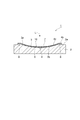
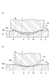
- FIG. 2 is an end view of the optical element taken along line II-II in FIG. 1. It is a top view of the board
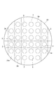
- FIG. 5 is a cross-sectional view of the substrate along the line VV in FIG. 4. It is a top view of the board
- the optical element 1 has an optical function unit 10 that is a reflective grating.
- the optical function unit 10 splits and reflects the light L incident from one side.
- the optical element 1 includes a base plate 2 made of silicon, plastic, ceramic, glass, or the like (for example, an outer shape of 8 mm ⁇ 8 mm and a thickness of 1 mm).
- a concave portion 3 having a spherical inner surface 3b is formed on the surface 2a of the substrate 2.
- the material of the base material 2 is not limited to the materials described above, and various materials can be applied and formed by molding, cutting, etching, or the like.
- the inner surface 3b of the recess 3 is not limited to a spherical shape but may be an aspherical shape.
- a molding layer 4 formed by photocuring a replicating optical resin such as a photocurable epoxy resin, acrylic resin, fluorine resin, silicone or organic-inorganic hybrid resin is disposed on the base material 2.
- the molding layer 4 has a circular shape when viewed from the depth direction (that is, one side) of the recess 3.
- the material of the molding layer 4 is not limited to the above-described photocurable resin material, but may be molded and cured by a molding die 30 described later, such as a thermosetting resin material, low-melting glass, or organic-inorganic hybrid glass.
- Various possible materials (molding materials) can be applied.
- the molding layer 4 has a body portion (first portion) 5 and a ride-up portion (second portion) 6 that are integrally formed.
- the main body 5 is located in the recess 3 when viewed from the depth direction of the recess 3, and covers the entire inner surface 3 b of the recess 3.
- the ride-up part 6 is located on the surface 2a of the base material 2 in a state of being connected to the main body part 5, and is provided outside the annular opening 3a. That is, the riding-up part 6 is provided so as to surround the recess 3.
- the thickness in the depth direction of the recess 3 in the ride-up portion 6 is thicker than the thickness in the depth direction of the recess 3 in the main body 5.
- a portion corresponding to the main body portion 5 of a surface (predetermined surface) 4 b opposite to the base material 2 side (hereinafter referred to as “surface” of the molding layer 4) has a concave curved surface shape.
- a curved surface 4c is provided.
- the curved surface 4 c is recessed in the same direction as the inner surface 3 b of the recess 3. That is, the portion of the main body portion 5 of the molding layer 4 is disposed along the inner surface 3 b of the concave portion 3 of the base material 2.
- a grating pattern corresponding to a blazed grating having a sawtooth cross section, a binary grating having a rectangular cross section, a holographic grating having a sinusoidal cross section, or the like is formed in a predetermined region on the main body 5 on the curved surface 4c.
- a reflective film 7 which is a vapor deposition film of Al or Au is formed on the surface 4b of the molding layer 4, a reflective film 7 which is a vapor deposition film of Al or Au is formed.
- the reflective film 7 is formed so as to correspond to the grating pattern in a predetermined region on the main body portion 5 on the surface 4b, and this portion is an optical function portion 10 that is a reflective grating.
- the material of the reflective film 7 is not limited to the above-described material, and various materials can be applied.
- SiO2, SiN, MgF2 or the like may be formed on the reflective film 7 as a protective film or antireflection film by vapor deposition, sputtering, CVD, or the like.
- an adhesion layer such as Cr, Ni, NiCr, Ti, TiN or the like may be formed between the molding layer 4 and the reflective film 7 by vapor deposition, sputtering, CVD, or the like.
- the curved surface 4 c which is the portion corresponding to the main body portion 5, of the surface 4 b of the molding layer 4 is recessed in the same direction as the inner surface 3 b of the recess 3 of the substrate 2.
- the change of the thickness of the molding layer 4 in the main body part 5 becomes moderate.
- the thickness of the molding layer 4 in the main body 5 is reduced (for example, 1 ⁇ m). ⁇ 100 ⁇ m).
- fever can be reduced. Further, even if stress generated due to temperature change or the like during use is concentrated on the concave portion 3 of the base material 2, the base portion 5 can be connected to the main body portion 5 by the riding portion 6 positioned on the surface 2 a of the base material 2. The main body 5 located in the recess 3 of the material 2 is pressed.
- the surface 2a on which the riding-up portion 6 is located is a surface discontinuous with the inner surface 3b of the concave portion 3 (in the optical element 1, the inner surface 3b of the concave portion 3 that is a curved surface and the surface that is a flat surface 2a is connected).
- the riding-up portion 6 is provided so as to surround the concave portion 3, the main body portion 5 is uniformly pressed from the periphery. Thereby, peeling of the shaping
- the shrinkage or expansion of the molding layer 4 due to temperature change during use is absorbed by the riding-up portion 6 located on the surface 2a of the base material 2, and the main body located in the concave portion 3 of the base material 2
- the contraction or expansion of the part 5 is alleviated.
- the riding-up portion 6 is provided so as to surround the concave portion 3, the contraction or expansion of the main body portion 5 is uniformly alleviated.
- the thickness of the riding-up portion 6 is formed to be thicker than the thickness of the main body portion 5. Accordingly, the deformation of the curved surface 4c of the main body 5 is reliably prevented, and further, the deformation of the optical function unit 10 provided on the curved surface 4c is reliably prevented. Therefore, according to the optical element 1, peeling of the molding layer 4 and deformation of the optical function unit 10 can be reliably prevented with a simple configuration.
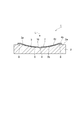
- a substrate 20 made of, for example, silicon is prepared.
- the substrate 20 becomes a plurality of base materials 2 by cutting (dicing) into a lattice shape.
- the recessed part 3 is formed in the surface 20a of the board
- FIG. Thereby, a plurality of base materials 2 having the recesses 3 formed on the surface 2a are prepared.
- a molding material here, a photocurable resin material
- the molding layer 4 is disposed on the surface 20 a of the substrate 20 for each of the recesses 3 of the base material 2. As a result, the molding material is disposed on the plurality of base materials 2.
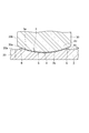
- the molding die 30 is pressed against the molding material for each recess 3 of the base 2.
- light for example, ultraviolet rays
- the molding layer 4 having Furthermore, the mold layer 4 may be thermally cured after the mold 30 is released from the mold layer 4.
- the base material 2 has permeability
- the curing method of the molding material is not limited to photocuring, and various curing methods such as thermal curing can be applied depending on the type of the molding material.
- the molding die 30 is not limited to one having transparency, and can be formed of a metal such as nickel.
- the molding die 30 has a molding surface 30 a for forming a curved surface 4 c on which the optical function unit 10 is provided on the surface 4 b of the molding layer 4.
- the molding surface 30a is a convex curved surface having a complementary relationship with the curved surface 4c.
- the reflective film 7 is formed on the surface 4b of the molding layer 4 by vapor-depositing Al or Au, and the optical function unit 10 is provided for each curved surface 4c.
- This vapor deposition is performed on the entire surface 4b or an arbitrary range (mask vapor deposition) of the surface 4b as necessary.
- the substrate 20 is cut (diced) into a lattice shape to obtain a plurality of optical elements 1 that are grating elements.
- the reflective film 7 may be formed by a sputtering method or a CVD method in addition to the vapor deposition method.
- the curved surface 4 c corresponding to the main body portion 5 of the surface 4 b of the molding layer 4 is recessed in the same direction as the inner surface 3 b of the recess 3 of the substrate 2.
- the change in the thickness of the molding layer 4 in the main body 5 is moderate.
- the thickness of the molding layer 4 in the main body portion 5 can be made constant.
- fever can be reduced.
- the ride-up portion 6 positioned on the surface 2 a of the base material 2 in a state of being connected to the main body portion 5 has priority over the main body portion 5. Due to the shrinkage, the shrinkage of the main body 5 located in the recess 3 of the substrate 2 is alleviated.
- the riding-up portion 6 is provided so as to surround the concave portion 3, the contraction of the main body portion 5 is uniformly alleviated. Thereby, the deformation of the curved surface 4c of the main body portion 5 is reliably prevented, and further, the deformation of the optical function portion 10 provided on the curved surface 4c is reliably prevented.
- the periphery of the molding surface 30a of the mold 30 can be shaped to protrude outward from the opening 3a of the recess 3.
- the tip of the molding die 30 is buried in the molding material, and the molding material can be prevented from reaching the side surface 30 b of the molding die 30.
- abuts only to the molding surface 30a, and the mold release property of the shaping
- the curvature of the inner surface 3 b of the recess 3 of the substrate 2 can be made larger than the curvature of the molding surface 30 a of the mold 30.
- molding die 30 does not contact
- FIG. 7A the curvature of the inner surface 3 b of the recess 3 of the substrate 2 can be made larger than the curvature of the molding surface 30 a of the mold 30.
- the curvature of the inner surface 3 b of the recess 3 of the substrate 2 can be made smaller than the curvature of the molding surface 30 a of the mold 30.
- molding layer 4 with the thin thickness of the center part of the main-body part 5 can be obtained.
- a groove (groove portion) 8 may be provided on the outer surface of the opening 3a of the recess 3 on the surface 2a of the substrate 2.
- the groove 8 can be an annular shape surrounding the recess 3.
- the molding material enters the groove 8 when the molding die 30 is pressed against the molding material arranged on the substrate 2. That is, when the molding material spreads outward from the recess 3, the molding material enters the groove 8, so that the spreading of the molding material is regulated.
- the riding-up portion 6 enters the groove 8.
- the spread of the raised portion 6 of the molding layer 4 on the surface 2a of the base material 2 can be controlled. Thereby, size reduction of the base material 2 or the recessed part 3 can be enlarged. Moreover, the fixed strength of the molding layer 4 with respect to the base material 2 can be improved because the riding-up portion 6 enters the groove 8.
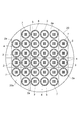
- the recess 3 is formed at a position outside the opening 3a of the recess 3 on the surface 2a of the substrate 2.
- Linear grooves 8a to 8d may be provided so as to surround.
- a predetermined gap is provided between the grooves 8a to 8d.
- a square frame-shaped groove 8 e may be provided on the surface 2 a of the substrate 2 at a position outside the opening 3 a of the recess 3 so as to surround the recess 3. Further, as shown in FIG.
- a pair of grooves 8f and 8g are provided on the surface 2a of the substrate 2 at a position outside the opening 3a of the recess 3 so as to sandwich the recess 3, and the groove 8f , 8g may be provided with grooves 8h, 8i connected to the outer edge of the substrate 2. Even in these cases, the molding material enters the groove, and the spread of the rising portion 6 of the molding layer 4 on the surface 2a of the substrate 2 can be controlled.
- the optical function unit 10 can have various optical functions without being limited to the grating.
- the optical function unit 10 may be a mirror without forming a grating pattern on the curved surface 4 c and the reflective film 7 of the molding layer 4. In that case, a mirror element with a simple configuration can be obtained.
- the refractive index may be matched at the interface between the substrate 2 and the molding layer 4 so that the light L is incident on the optical function unit 10 from the substrate 2 side (the other side). Further, when the light L is incident from either one side or the other side, the light L may be transmitted to the optical function unit 10 (for example, a transmissive grating) without providing the reflective film 7. Good.
- the predetermined surface of the molding layer 4 on which the optical function unit 10 is provided is not limited to the curved surface 4c, but may be a part of the surface 4b from the main body 5 to the riding-up unit 6.
- the riding-up portion 6 is formed in an annular shape so as to surround the concave portion 3, but is not limited to an annular shape, and may be provided biased to only one side. .
- a recess may be provided on the surface 2a of the substrate 2.
- a rectangular concave portion or a circular concave portion can be adopted. Even in this case, the fixing strength of the molding layer 4 can be improved by the ride-in portion 6 entering the recess provided instead of the groove 8.
- the recess 3 is sandwiched between the recesses 3 on the diagonal of the substrate 2.
- the substrate 20 is cut (diced) in a lattice shape to obtain a plurality of optical elements 1, the optical elements 1 can be formed one by one.
- an optical element that can prevent peeling of a molding layer and deformation of an optical function part, and a method for manufacturing the same.
- SYMBOLS 1 Optical element, 2 ... Base material, 2a ... Surface, 3 ... Recessed part, 3a ... Opening, 3b ... Inner surface, 4 ... Molding layer, 4b ... Surface (predetermined surface), 4c ... Curved surface (opposite surface), DESCRIPTION OF SYMBOLS 5 ... Main-body part (1st part), 6 ... Riding part (2nd part), 8, 8a-8i ... Groove (groove part), 10 ... Optical function part, 30 ... Mold, 30a ... Molding surface.
Landscapes
- Physics & Mathematics (AREA)
- General Physics & Mathematics (AREA)
- Optics & Photonics (AREA)
- Engineering & Computer Science (AREA)
- Mechanical Engineering (AREA)
- Manufacturing & Machinery (AREA)
- Health & Medical Sciences (AREA)
- Ophthalmology & Optometry (AREA)
- Diffracting Gratings Or Hologram Optical Elements (AREA)
- Optical Elements Other Than Lenses (AREA)
- Moulds For Moulding Plastics Or The Like (AREA)
Priority Applications (4)
| Application Number | Priority Date | Filing Date | Title |
|---|---|---|---|
| CN201380040133.5A CN104508519B (zh) | 2012-08-06 | 2013-06-13 | 光学元件及其制造方法 |
| US14/418,962 US9594197B2 (en) | 2012-08-06 | 2013-06-13 | Optical element, and method for producing same |
| EP13828733.9A EP2881768B1 (en) | 2012-08-06 | 2013-06-13 | Optical element, and method for producing same |
| US15/435,354 US10386552B2 (en) | 2012-08-06 | 2017-02-17 | Optical element, and method for producing same |
Applications Claiming Priority (2)
| Application Number | Priority Date | Filing Date | Title |
|---|---|---|---|
| JP2012-174324 | 2012-08-06 | ||
| JP2012174324A JP6234667B2 (ja) | 2012-08-06 | 2012-08-06 | 光学素子及びその製造方法 |
Related Child Applications (3)
| Application Number | Title | Priority Date | Filing Date |
|---|---|---|---|
| US14/418,962 A-371-Of-International US9594197B2 (en) | 2012-08-06 | 2013-06-13 | Optical element, and method for producing same |
| US201514418962A A-371-Of-International | 2012-08-06 | 2015-02-02 | |
| US15/435,354 Continuation US10386552B2 (en) | 2012-08-06 | 2017-02-17 | Optical element, and method for producing same |
Publications (1)
| Publication Number | Publication Date |
|---|---|
| WO2014024565A1 true WO2014024565A1 (ja) | 2014-02-13 |
Family
ID=50067807
Family Applications (1)
| Application Number | Title | Priority Date | Filing Date |
|---|---|---|---|
| PCT/JP2013/066326 Ceased WO2014024565A1 (ja) | 2012-08-06 | 2013-06-13 | 光学素子及びその製造方法 |
Country Status (6)
| Country | Link |
|---|---|
| US (2) | US9594197B2 (enExample) |
| EP (1) | EP2881768B1 (enExample) |
| JP (1) | JP6234667B2 (enExample) |
| CN (1) | CN104508519B (enExample) |
| TW (1) | TWI607247B (enExample) |
| WO (1) | WO2014024565A1 (enExample) |
Cited By (2)
| Publication number | Priority date | Publication date | Assignee | Title |
|---|---|---|---|---|
| JP2016081054A (ja) * | 2014-10-13 | 2016-05-16 | 台達電子工業股▲ふん▼有限公司Delta Electronics,Inc. | 光波長変換デバイス及びこれを用いた照明システム |
| CN109852930A (zh) * | 2019-03-29 | 2019-06-07 | 中国科学院上海技术物理研究所 | 一种补偿中口径介质膜平面反射镜镀膜形变的方法 |
Families Citing this family (5)
| Publication number | Priority date | Publication date | Assignee | Title |
|---|---|---|---|---|
| JP6188743B2 (ja) | 2014-06-19 | 2017-08-30 | キヤノン株式会社 | 複数の光学機能面を有する光学素子、分光装置およびその製造方法 |
| HUE060361T2 (hu) * | 2015-11-16 | 2023-02-28 | Dexerials Corp | Optikai test, mesterdarab, valamint eljárás optikai test gyártására |
| US11934028B2 (en) * | 2018-10-11 | 2024-03-19 | Mitsubishi Electric Corporation | Optical multiplexer/demultiplexer |
| CN110927835A (zh) * | 2019-12-31 | 2020-03-27 | 上海理工大学 | 利用应变调制自组装制作光栅微透镜阵列的方法及产品 |
| CN114274544A (zh) * | 2021-12-24 | 2022-04-05 | 中国科学院长春光学精密机械与物理研究所 | 一种采用可变曲率模具制备复合材料反射镜的方法 |
Citations (8)
| Publication number | Priority date | Publication date | Assignee | Title |
|---|---|---|---|---|
| JPH0772310A (ja) * | 1993-09-06 | 1995-03-17 | Nikon Corp | 非球面光学素子の製造方法 |
| JP2003266450A (ja) | 2002-03-18 | 2003-09-24 | Canon Inc | 光学素子及びその製造方法 |
| JP2005173597A (ja) | 2003-12-06 | 2005-06-30 | Samsung Electronics Co Ltd | 回折レンズアレイモールドの製造方法、及びそれに用いられるuv照射器 |
| JP2005520213A (ja) | 2002-05-30 | 2005-07-07 | インターナショナル・ビジネス・マシーンズ・コーポレーション | パターニング方法 |
| JP2006177994A (ja) | 2004-12-20 | 2006-07-06 | Shimadzu Corp | レプリカ光学素子 |
| JP2007199540A (ja) | 2006-01-30 | 2007-08-09 | Shimadzu Corp | 反射型レプリカ光学素子 |
| JP2011215074A (ja) * | 2010-04-01 | 2011-10-27 | Hamamatsu Photonics Kk | 分光モジュール |
| JP2012063764A (ja) * | 2010-08-20 | 2012-03-29 | Citizen Holdings Co Ltd | 光学構造を備えた基板及びそれを用いた光学素子 |
Family Cites Families (36)
| Publication number | Priority date | Publication date | Assignee | Title |
|---|---|---|---|---|
| US4012843A (en) * | 1973-04-25 | 1977-03-22 | Hitachi, Ltd. | Concave diffraction grating and a manufacturing method thereof |
| FI54029C (fi) * | 1974-06-04 | 1978-09-11 | Nils Allan Danielsson | Saett vid aostadkommande av stigmatisk avbildning vid spektralanalys med ett konkavgitter |
| US4192994A (en) * | 1978-09-18 | 1980-03-11 | The United States Of America As Represented By The Administrator Of The National Aeronautics And Space Administration | Diffractoid grating configuration for X-ray and ultraviolet focusing |
| JPS55136918A (en) * | 1979-04-13 | 1980-10-25 | Hitachi Ltd | Aberration correcting recess diffraction grating |
| US4798446A (en) * | 1987-09-14 | 1989-01-17 | The United States Of America As Represented By The United States Department Of Energy | Aplanatic and quasi-aplanatic diffraction gratings |
| US5543966A (en) * | 1993-12-29 | 1996-08-06 | Eastman Kodak Company | Hybrid refractive/diffractive achromatic camera lens |
| DE4434814A1 (de) * | 1994-09-29 | 1996-04-04 | Microparts Gmbh | Infrarotspektrometrischer Sensor für Gase |
| WO1998032036A1 (en) * | 1997-01-17 | 1998-07-23 | Cymer, Inc. | Reflective overcoat for replicated diffraction gratings |
| EP2261919A3 (en) * | 1998-02-23 | 2011-03-09 | Kabushiki Kaisha Toshiba | Information storage medium, information playback method and apparatus and information recording method |
| JP3865516B2 (ja) * | 1998-10-23 | 2007-01-10 | ソニー株式会社 | 全方位撮像装置 |
| TW473615B (en) | 1999-07-23 | 2002-01-21 | Nippon Kogaku Kk | Resin-bonded type optical element, production method therefor and optical article |
| US6473232B2 (en) | 2000-03-08 | 2002-10-29 | Canon Kabushiki Kaisha | Optical system having a diffractive optical element, and optical apparatus |
| JP4587418B2 (ja) * | 2000-09-27 | 2010-11-24 | キヤノン株式会社 | 回折光学素子及び該回折光学素子を有する光学系 |
| US20020163688A1 (en) * | 2001-03-26 | 2002-11-07 | Zuhua Zhu | Optical communications system and vertical cavity surface emitting laser therefor |
| US6534903B1 (en) * | 2002-02-25 | 2003-03-18 | General Electric Company | Broad spectrum reflective coating for an electric lamp |
| WO2004049027A1 (ja) * | 2002-11-26 | 2004-06-10 | Fujitsu Limited | 光合分波器 |
| US7054065B2 (en) * | 2003-03-27 | 2006-05-30 | The Regents Of The University Of California | Durable silver thin film coating for diffraction gratings |
| JP4387855B2 (ja) * | 2004-04-01 | 2009-12-24 | キヤノン株式会社 | 光学系 |
| US20050286570A1 (en) * | 2004-06-29 | 2005-12-29 | Lian-Qin Xiang | Tunable laser with a concave diffraction grating |
| US9146155B2 (en) * | 2007-03-15 | 2015-09-29 | Oto Photonics, Inc. | Optical system and manufacturing method thereof |
| US7656585B1 (en) * | 2008-08-19 | 2010-02-02 | Microvision, Inc. | Embedded relay lens for head-up displays or the like |
| JP5205239B2 (ja) * | 2008-05-15 | 2013-06-05 | 浜松ホトニクス株式会社 | 分光器 |
| JP5207938B2 (ja) * | 2008-05-15 | 2013-06-12 | 浜松ホトニクス株式会社 | 分光モジュール及び分光モジュールの製造方法 |
| JP5205241B2 (ja) * | 2008-05-15 | 2013-06-05 | 浜松ホトニクス株式会社 | 分光モジュール |
| JP5415060B2 (ja) * | 2008-05-15 | 2014-02-12 | 浜松ホトニクス株式会社 | 分光モジュール |
| JP5205242B2 (ja) * | 2008-05-15 | 2013-06-05 | 浜松ホトニクス株式会社 | 分光器の製造方法 |
| TWI425203B (zh) * | 2008-09-03 | 2014-02-01 | Univ Nat Central | 高頻譜掃描裝置及其方法 |
| FR2945159B1 (fr) * | 2009-04-29 | 2016-04-01 | Horiba Jobin Yvon Sas | Reseau de diffraction metallique en reflexion a haute tenue au flux en regime femtoseconde, systeme comprenant un tel reseau et procede d'amelioration du seuil d'endommagement d'un reseau de diffraction metallique |
| JP5411778B2 (ja) * | 2009-04-30 | 2014-02-12 | キヤノン株式会社 | 分光測色装置、およびそれを用いた画像形成装置 |
| EP2444826B1 (en) * | 2009-06-18 | 2019-05-22 | Toppan Printing Co., Ltd. | Optical device and method of manufacturing the same |
| JP5421684B2 (ja) * | 2009-07-29 | 2014-02-19 | キヤノン株式会社 | 回折光学素子、それを用いた分光測色装置および画像形成装置 |
| JP5592089B2 (ja) * | 2009-08-19 | 2014-09-17 | 浜松ホトニクス株式会社 | 分光モジュール及びその製造方法 |
| DE102009046831B4 (de) * | 2009-11-18 | 2015-02-12 | Fraunhofer-Gesellschaft zur Förderung der angewandten Forschung e.V. | Strahlungserzeugungsvorrichtung zum Erzeugen einer elektromagnetischen Strahlung mit einer einstellbaren spektralen Zusammensetzung und Verfahren zur Herstellung derselben |
| JP2012013530A (ja) * | 2010-06-30 | 2012-01-19 | Fujifilm Corp | 回折格子及びその製造方法、並びに放射線撮影装置 |
| TWI536051B (zh) * | 2011-02-08 | 2016-06-01 | Hamamatsu Photonics Kk | Optical element and manufacturing method thereof |
| JP5767882B2 (ja) * | 2011-07-26 | 2015-08-26 | 浜松ホトニクス株式会社 | 分光器 |
-
2012
- 2012-08-06 JP JP2012174324A patent/JP6234667B2/ja active Active
-
2013
- 2013-06-13 WO PCT/JP2013/066326 patent/WO2014024565A1/ja not_active Ceased
- 2013-06-13 EP EP13828733.9A patent/EP2881768B1/en active Active
- 2013-06-13 US US14/418,962 patent/US9594197B2/en active Active
- 2013-06-13 CN CN201380040133.5A patent/CN104508519B/zh active Active
- 2013-08-02 TW TW102127855A patent/TWI607247B/zh active
-
2017
- 2017-02-17 US US15/435,354 patent/US10386552B2/en active Active
Patent Citations (8)
| Publication number | Priority date | Publication date | Assignee | Title |
|---|---|---|---|---|
| JPH0772310A (ja) * | 1993-09-06 | 1995-03-17 | Nikon Corp | 非球面光学素子の製造方法 |
| JP2003266450A (ja) | 2002-03-18 | 2003-09-24 | Canon Inc | 光学素子及びその製造方法 |
| JP2005520213A (ja) | 2002-05-30 | 2005-07-07 | インターナショナル・ビジネス・マシーンズ・コーポレーション | パターニング方法 |
| JP2005173597A (ja) | 2003-12-06 | 2005-06-30 | Samsung Electronics Co Ltd | 回折レンズアレイモールドの製造方法、及びそれに用いられるuv照射器 |
| JP2006177994A (ja) | 2004-12-20 | 2006-07-06 | Shimadzu Corp | レプリカ光学素子 |
| JP2007199540A (ja) | 2006-01-30 | 2007-08-09 | Shimadzu Corp | 反射型レプリカ光学素子 |
| JP2011215074A (ja) * | 2010-04-01 | 2011-10-27 | Hamamatsu Photonics Kk | 分光モジュール |
| JP2012063764A (ja) * | 2010-08-20 | 2012-03-29 | Citizen Holdings Co Ltd | 光学構造を備えた基板及びそれを用いた光学素子 |
Non-Patent Citations (1)
| Title |
|---|
| See also references of EP2881768A4 |
Cited By (3)
| Publication number | Priority date | Publication date | Assignee | Title |
|---|---|---|---|---|
| JP2016081054A (ja) * | 2014-10-13 | 2016-05-16 | 台達電子工業股▲ふん▼有限公司Delta Electronics,Inc. | 光波長変換デバイス及びこれを用いた照明システム |
| CN109852930A (zh) * | 2019-03-29 | 2019-06-07 | 中国科学院上海技术物理研究所 | 一种补偿中口径介质膜平面反射镜镀膜形变的方法 |
| CN109852930B (zh) * | 2019-03-29 | 2021-06-15 | 中国科学院上海技术物理研究所 | 一种补偿中口径介质膜平面反射镜镀膜形变的方法 |
Also Published As
| Publication number | Publication date |
|---|---|
| CN104508519A (zh) | 2015-04-08 |
| US10386552B2 (en) | 2019-08-20 |
| US20170160449A1 (en) | 2017-06-08 |
| JP6234667B2 (ja) | 2017-11-22 |
| TWI607247B (zh) | 2017-12-01 |
| CN104508519B (zh) | 2018-04-03 |
| EP2881768A4 (en) | 2016-04-06 |
| EP2881768B1 (en) | 2024-08-14 |
| TW201411199A (zh) | 2014-03-16 |
| JP2014032368A (ja) | 2014-02-20 |
| US20150205017A1 (en) | 2015-07-23 |
| US9594197B2 (en) | 2017-03-14 |
| EP2881768A1 (en) | 2015-06-10 |
Similar Documents
| Publication | Publication Date | Title |
|---|---|---|
| JP6234667B2 (ja) | 光学素子及びその製造方法 | |
| JP4944652B2 (ja) | 回折光学素子及びそれを用いた光学系 | |
| JP5996440B2 (ja) | 光学素子及びその製造方法 | |
| CN102037383B (zh) | 包括至少一个复制面的光学器件及其相关方法 | |
| US20140376097A1 (en) | Microlens array and imaging element package | |
| WO2009139327A1 (ja) | 分光器の製造方法 | |
| JP2009028952A (ja) | 光学素子の製造方法 | |
| JP2002071923A (ja) | 回折光学素子の製造方法及び回折光学素子、並びに該回折光学素子を有する光学系、該光学系を有する撮影装置と観察装置 | |
| JP5159620B2 (ja) | 複合光学素子 | |
| JP2006106229A (ja) | 透過型光学素子の製造方法および透過型光学素子 | |
| TWI402162B (zh) | 複合微透鏡及複合微透鏡陣列 | |
| JP2003262713A (ja) | 回折光学素子及び回折光学素子の製造方法 | |
| JP2014215375A (ja) | レプリカ回折格子及びその製造方法 | |
| JP2013205534A (ja) | 回折光学素子及びその製造方法並びに回折光学素子を用いた光学系 | |
| JP4320708B2 (ja) | 光学素子の製造方法 | |
| US10175462B2 (en) | Wafer level lens system and method of fabricating the same | |
| JP7761007B2 (ja) | 光学素子 | |
| JPWO2012114408A1 (ja) | 回折光学素子およびそれを備えた撮像装置 | |
| JP2003307608A (ja) | 回折光学素子の製造方法 | |
| CN111356948A (zh) | 微器件和相关两件式器件,特别是微光学系统的晶片级制造 | |
| JP2007309964A (ja) | 複合光学素子及びその製造方法 | |
| JP2013029813A (ja) | 回折光学素子及びそれを備えた撮像装置 | |
| JP2011191395A (ja) | 光学素子 | |
| TWI498618B (zh) | 光波導之製法(二) | |
| JP2007333859A (ja) | 複合光学素子及びその製造方法 |
Legal Events
| Date | Code | Title | Description |
|---|---|---|---|
| 121 | Ep: the epo has been informed by wipo that ep was designated in this application |
Ref document number: 13828733 Country of ref document: EP Kind code of ref document: A1 |
|
| WWE | Wipo information: entry into national phase |
Ref document number: 2013828733 Country of ref document: EP |
|
| WWE | Wipo information: entry into national phase |
Ref document number: 14418962 Country of ref document: US |
|
| NENP | Non-entry into the national phase |
Ref country code: DE |