WO2014021186A1 - 配線基板、それを備えた実装構造体および配線基板の製造方法 - Google Patents
配線基板、それを備えた実装構造体および配線基板の製造方法 Download PDFInfo
- Publication number
- WO2014021186A1 WO2014021186A1 PCT/JP2013/070173 JP2013070173W WO2014021186A1 WO 2014021186 A1 WO2014021186 A1 WO 2014021186A1 JP 2013070173 W JP2013070173 W JP 2013070173W WO 2014021186 A1 WO2014021186 A1 WO 2014021186A1
- Authority
- WO
- WIPO (PCT)
- Prior art keywords
- resin
- layer
- inorganic insulating
- insulating particles
- wiring board
- Prior art date
- Legal status (The legal status is an assumption and is not a legal conclusion. Google has not performed a legal analysis and makes no representation as to the accuracy of the status listed.)
- Ceased
Links
Images





Classifications
-
- H—ELECTRICITY
- H05—ELECTRIC TECHNIQUES NOT OTHERWISE PROVIDED FOR
- H05K—PRINTED CIRCUITS; CASINGS OR CONSTRUCTIONAL DETAILS OF ELECTRIC APPARATUS; MANUFACTURE OF ASSEMBLAGES OF ELECTRICAL COMPONENTS
- H05K1/00—Printed circuits
- H05K1/02—Details
- H05K1/11—Printed elements for providing electric connections to or between printed circuits
- H05K1/111—Pads for surface mounting, e.g. lay-out
- H05K1/112—Pads for surface mounting, e.g. lay-out directly combined with via connections
-
- H—ELECTRICITY
- H05—ELECTRIC TECHNIQUES NOT OTHERWISE PROVIDED FOR
- H05K—PRINTED CIRCUITS; CASINGS OR CONSTRUCTIONAL DETAILS OF ELECTRIC APPARATUS; MANUFACTURE OF ASSEMBLAGES OF ELECTRICAL COMPONENTS
- H05K1/00—Printed circuits
- H05K1/02—Details
- H05K1/0296—Conductive pattern lay-out details not covered by sub groups H05K1/02 - H05K1/0295
- H05K1/0298—Multilayer circuits
-
- H—ELECTRICITY
- H05—ELECTRIC TECHNIQUES NOT OTHERWISE PROVIDED FOR
- H05K—PRINTED CIRCUITS; CASINGS OR CONSTRUCTIONAL DETAILS OF ELECTRIC APPARATUS; MANUFACTURE OF ASSEMBLAGES OF ELECTRICAL COMPONENTS
- H05K1/00—Printed circuits
- H05K1/18—Printed circuits structurally associated with non-printed electric components
- H05K1/181—Printed circuits structurally associated with non-printed electric components associated with surface mounted components
-
- H—ELECTRICITY
- H05—ELECTRIC TECHNIQUES NOT OTHERWISE PROVIDED FOR
- H05K—PRINTED CIRCUITS; CASINGS OR CONSTRUCTIONAL DETAILS OF ELECTRIC APPARATUS; MANUFACTURE OF ASSEMBLAGES OF ELECTRICAL COMPONENTS
- H05K3/00—Apparatus or processes for manufacturing printed circuits
- H05K3/46—Manufacturing multilayer circuits
- H05K3/4602—Manufacturing multilayer circuits characterized by a special circuit board as base or central core whereon additional circuit layers are built or additional circuit boards are laminated
-
- H—ELECTRICITY
- H05—ELECTRIC TECHNIQUES NOT OTHERWISE PROVIDED FOR
- H05K—PRINTED CIRCUITS; CASINGS OR CONSTRUCTIONAL DETAILS OF ELECTRIC APPARATUS; MANUFACTURE OF ASSEMBLAGES OF ELECTRICAL COMPONENTS
- H05K3/00—Apparatus or processes for manufacturing printed circuits
- H05K3/46—Manufacturing multilayer circuits
- H05K3/4644—Manufacturing multilayer circuits by building the multilayer layer by layer, i.e. build-up multilayer circuits
- H05K3/4652—Adding a circuit layer by laminating a metal foil or a preformed metal foil pattern
- H05K3/4655—Adding a circuit layer by laminating a metal foil or a preformed metal foil pattern by using a laminate characterized by the insulating layer
-
- H—ELECTRICITY
- H10—SEMICONDUCTOR DEVICES; ELECTRIC SOLID-STATE DEVICES NOT OTHERWISE PROVIDED FOR
- H10W—GENERIC PACKAGES, INTERCONNECTIONS, CONNECTORS OR OTHER CONSTRUCTIONAL DETAILS OF DEVICES COVERED BY CLASS H10
- H10W70/00—Package substrates; Interposers; Redistribution layers [RDL]
- H10W70/60—Insulating or insulated package substrates; Interposers; Redistribution layers
- H10W70/62—Insulating or insulated package substrates; Interposers; Redistribution layers characterised by their interconnections
- H10W70/63—Vias, e.g. via plugs
- H10W70/635—Through-vias
-
- H—ELECTRICITY
- H10—SEMICONDUCTOR DEVICES; ELECTRIC SOLID-STATE DEVICES NOT OTHERWISE PROVIDED FOR
- H10W—GENERIC PACKAGES, INTERCONNECTIONS, CONNECTORS OR OTHER CONSTRUCTIONAL DETAILS OF DEVICES COVERED BY CLASS H10
- H10W70/00—Package substrates; Interposers; Redistribution layers [RDL]
- H10W70/60—Insulating or insulated package substrates; Interposers; Redistribution layers
- H10W70/67—Insulating or insulated package substrates; Interposers; Redistribution layers characterised by their insulating layers or insulating parts
- H10W70/68—Shapes or dispositions thereof
- H10W70/685—Shapes or dispositions thereof comprising multiple insulating layers
-
- H—ELECTRICITY
- H10—SEMICONDUCTOR DEVICES; ELECTRIC SOLID-STATE DEVICES NOT OTHERWISE PROVIDED FOR
- H10W—GENERIC PACKAGES, INTERCONNECTIONS, CONNECTORS OR OTHER CONSTRUCTIONAL DETAILS OF DEVICES COVERED BY CLASS H10
- H10W70/00—Package substrates; Interposers; Redistribution layers [RDL]
- H10W70/60—Insulating or insulated package substrates; Interposers; Redistribution layers
- H10W70/67—Insulating or insulated package substrates; Interposers; Redistribution layers characterised by their insulating layers or insulating parts
- H10W70/69—Insulating materials thereof
-
- H—ELECTRICITY
- H10—SEMICONDUCTOR DEVICES; ELECTRIC SOLID-STATE DEVICES NOT OTHERWISE PROVIDED FOR
- H10W—GENERIC PACKAGES, INTERCONNECTIONS, CONNECTORS OR OTHER CONSTRUCTIONAL DETAILS OF DEVICES COVERED BY CLASS H10
- H10W70/00—Package substrates; Interposers; Redistribution layers [RDL]
- H10W70/60—Insulating or insulated package substrates; Interposers; Redistribution layers
- H10W70/67—Insulating or insulated package substrates; Interposers; Redistribution layers characterised by their insulating layers or insulating parts
- H10W70/69—Insulating materials thereof
- H10W70/695—Organic materials
-
- H—ELECTRICITY
- H05—ELECTRIC TECHNIQUES NOT OTHERWISE PROVIDED FOR
- H05K—PRINTED CIRCUITS; CASINGS OR CONSTRUCTIONAL DETAILS OF ELECTRIC APPARATUS; MANUFACTURE OF ASSEMBLAGES OF ELECTRICAL COMPONENTS
- H05K2201/00—Indexing scheme relating to printed circuits covered by H05K1/00
- H05K2201/01—Dielectrics
- H05K2201/0137—Materials
- H05K2201/0175—Inorganic, non-metallic layer, e.g. resist or dielectric for printed capacitor
-
- H—ELECTRICITY
- H05—ELECTRIC TECHNIQUES NOT OTHERWISE PROVIDED FOR
- H05K—PRINTED CIRCUITS; CASINGS OR CONSTRUCTIONAL DETAILS OF ELECTRIC APPARATUS; MANUFACTURE OF ASSEMBLAGES OF ELECTRICAL COMPONENTS
- H05K2201/00—Indexing scheme relating to printed circuits covered by H05K1/00
- H05K2201/01—Dielectrics
- H05K2201/0183—Dielectric layers
- H05K2201/0195—Dielectric or adhesive layers comprising a plurality of layers, e.g. in a multilayer structure
-
- H—ELECTRICITY
- H05—ELECTRIC TECHNIQUES NOT OTHERWISE PROVIDED FOR
- H05K—PRINTED CIRCUITS; CASINGS OR CONSTRUCTIONAL DETAILS OF ELECTRIC APPARATUS; MANUFACTURE OF ASSEMBLAGES OF ELECTRICAL COMPONENTS
- H05K2201/00—Indexing scheme relating to printed circuits covered by H05K1/00
- H05K2201/02—Fillers; Particles; Fibers; Reinforcement materials
- H05K2201/0203—Fillers and particles
- H05K2201/0206—Materials
- H05K2201/0209—Inorganic, non-metallic particles
-
- H—ELECTRICITY
- H05—ELECTRIC TECHNIQUES NOT OTHERWISE PROVIDED FOR
- H05K—PRINTED CIRCUITS; CASINGS OR CONSTRUCTIONAL DETAILS OF ELECTRIC APPARATUS; MANUFACTURE OF ASSEMBLAGES OF ELECTRICAL COMPONENTS
- H05K2201/00—Indexing scheme relating to printed circuits covered by H05K1/00
- H05K2201/02—Fillers; Particles; Fibers; Reinforcement materials
- H05K2201/0203—Fillers and particles
- H05K2201/0263—Details about a collection of particles
- H05K2201/0269—Non-uniform distribution or concentration of particles
-
- H—ELECTRICITY
- H05—ELECTRIC TECHNIQUES NOT OTHERWISE PROVIDED FOR
- H05K—PRINTED CIRCUITS; CASINGS OR CONSTRUCTIONAL DETAILS OF ELECTRIC APPARATUS; MANUFACTURE OF ASSEMBLAGES OF ELECTRICAL COMPONENTS
- H05K2201/00—Indexing scheme relating to printed circuits covered by H05K1/00
- H05K2201/02—Fillers; Particles; Fibers; Reinforcement materials
- H05K2201/0275—Fibers and reinforcement materials
- H05K2201/029—Woven fibrous reinforcement or textile
-
- H—ELECTRICITY
- H10—SEMICONDUCTOR DEVICES; ELECTRIC SOLID-STATE DEVICES NOT OTHERWISE PROVIDED FOR
- H10W—GENERIC PACKAGES, INTERCONNECTIONS, CONNECTORS OR OTHER CONSTRUCTIONAL DETAILS OF DEVICES COVERED BY CLASS H10
- H10W70/00—Package substrates; Interposers; Redistribution layers [RDL]
- H10W70/60—Insulating or insulated package substrates; Interposers; Redistribution layers
- H10W70/62—Insulating or insulated package substrates; Interposers; Redistribution layers characterised by their interconnections
- H10W70/65—Shapes or dispositions of interconnections
- H10W70/654—Top-view layouts
- H10W70/655—Fan-out layouts
-
- H—ELECTRICITY
- H10—SEMICONDUCTOR DEVICES; ELECTRIC SOLID-STATE DEVICES NOT OTHERWISE PROVIDED FOR
- H10W—GENERIC PACKAGES, INTERCONNECTIONS, CONNECTORS OR OTHER CONSTRUCTIONAL DETAILS OF DEVICES COVERED BY CLASS H10
- H10W72/00—Interconnections or connectors in packages
- H10W72/071—Connecting or disconnecting
- H10W72/072—Connecting or disconnecting of bump connectors
- H10W72/07251—Connecting or disconnecting of bump connectors characterised by changes in properties of the bump connectors during connecting
-
- H—ELECTRICITY
- H10—SEMICONDUCTOR DEVICES; ELECTRIC SOLID-STATE DEVICES NOT OTHERWISE PROVIDED FOR
- H10W—GENERIC PACKAGES, INTERCONNECTIONS, CONNECTORS OR OTHER CONSTRUCTIONAL DETAILS OF DEVICES COVERED BY CLASS H10
- H10W72/00—Interconnections or connectors in packages
- H10W72/20—Bump connectors, e.g. solder bumps or copper pillars; Dummy bumps; Thermal bumps
-
- H—ELECTRICITY
- H10—SEMICONDUCTOR DEVICES; ELECTRIC SOLID-STATE DEVICES NOT OTHERWISE PROVIDED FOR
- H10W—GENERIC PACKAGES, INTERCONNECTIONS, CONNECTORS OR OTHER CONSTRUCTIONAL DETAILS OF DEVICES COVERED BY CLASS H10
- H10W90/00—Package configurations
- H10W90/701—Package configurations characterised by the relative positions of pads or connectors relative to package parts
- H10W90/721—Package configurations characterised by the relative positions of pads or connectors relative to package parts of bump connectors
- H10W90/724—Package configurations characterised by the relative positions of pads or connectors relative to package parts of bump connectors between a chip and a stacked insulating package substrate, interposer or RDL
Definitions
- the present invention relates to a wiring board used for an electronic device, a mounting structure including the wiring board, and a method for manufacturing the wiring board.
- Japanese Patent Application Laid-Open No. 2011-187473 discloses a wiring board including a conductive layer and a resin layer covering the conductive layer.
- the resin layer includes a resin portion and inorganic insulating particles dispersed in the resin portion, and is in contact with one main surface and a side surface of the conductive layer.
- the adhesive strength between the inorganic insulating particles and the resin part is small.
- solder reflow is performed when electronic components are mounted on the wiring board, heat is applied to the wiring board.
- the thermal stress resulting from the difference between the thermal expansion coefficient of the conductive layer and the thermal expansion coefficient of the resin layer tends to concentrate in the vicinity of the corner portion between the one main surface and the side surface of the conductive layer.
- a crack may occur from the corner portion toward the bonding surface between the resin portion having a low bonding strength and the inorganic insulating particles.
- this crack is likely to occur.
- An object of the present invention is to provide a wiring board with improved electrical reliability, a mounting structure including the wiring board, and a method for manufacturing the wiring board.
- a wiring board includes a first conductive layer and a first resin layer that includes a resin portion and a plurality of inorganic insulating particles dispersed in the resin portion and covers the first conductive layer.
- the first resin layer includes a first layer region in contact with one main surface and a side surface of the first conductive layer, and a second layer region located on the opposite side of the first conductive layer from the first conductive layer. It has.
- the plurality of inorganic insulating particles include a plurality of first inorganic insulating particles arranged in the first layer region and a plurality of second inorganic insulating particles arranged in the second layer region. The content ratio of the first inorganic insulating particles in the first layer region is smaller than the content ratio of the second inorganic insulating particles in the second layer region.
- the electrical reliability of the wiring board can be improved.
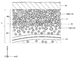
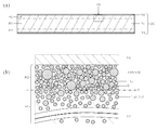
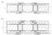
- (A) And (b) is sectional drawing cut
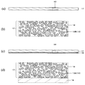
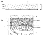
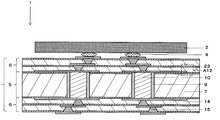
- (A) And (b) is sectional drawing cut
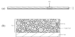
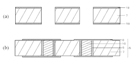
- (A) And (b) is sectional drawing cut
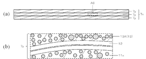
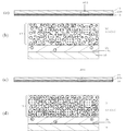
- A) And (b) is sectional drawing cut
- (b) is an enlarged view of A9 part of (a).
- (A) And (b) is sectional drawing cut
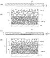
- (A) to (d) are cross-sectional views cut in the thickness direction for explaining the manufacturing process of the mounting structure shown in FIG. 1, respectively,
- (b) is an enlarged view of A10 portion of (a),
- (D) is an enlarged view of A11 part of (c).
- (A) And (b) is sectional drawing cut
- (A) And (b) is sectional drawing cut
- FIG. 14 It is sectional drawing which cut
- the mounting structure 1 shown in FIG. 1 is used for electronic devices such as various audiovisual devices, home appliances, communication devices, computer devices, and peripheral devices thereof.
- the mounting structure 1 includes an electronic component 2 and a wiring board 3 on which the electronic component 2 is mounted on one main surface.
- the electronic component 2 is, for example, a semiconductor element such as an IC, LSI, CMOS, or LED, or an acoustic wave element such as a SAW device.
- the electronic component 2 is flip-chip mounted on the wiring board 3 via bumps 4 made of a conductive material such as solder.
- the electronic component 2 is made of, for example, a semiconductor material such as silicon, germanium, gallium arsenide, gallium arsenide phosphorus, gallium nitride, or silicon carbide.
- the wiring board 3 supports the electronic component 2 and has a function of supplying power and signals for driving or controlling the electronic component 2 to the electronic component 2.
- the wiring substrate 3 includes a core substrate 5 and a pair of buildup layers 6 formed on both main surfaces of the core substrate 5.
- the core substrate 5 includes a base body 7, a pair of conductive layers 8 formed on both main surfaces of the base body 7, and a cylindrical through-hole conductor that penetrates the base body 7 and is electrically connected to each other. 9 and an insulator 10 filled inside the through-hole conductor 9.
- the base body 7 includes a first resin part 11, a base material 12 covered with the first resin part 11, and a plurality of first inorganic insulating particles arranged in the first resin part 11. 13A and a plurality of second inorganic insulating particles 13B (hereinafter also referred to as a plurality of inorganic insulating particles 13).
- the base body 7 includes a first layer region R1 and a pair of second layer regions R2 located on both main surfaces of the first layer region R1.
- region R1 has the 1st resin part 11, the base material 12 distribute
- the second layer region R2 includes a first resin part 11 and a plurality of second inorganic insulating particles 13B arranged in the first resin part 11.
- the second layer region R2 of the present embodiment does not include the base material 12.
- a boundary surface S in which the first inorganic insulating particles 13A or the second inorganic insulating particles 13B are aligned is formed between the first layer region R1 and the second layer region R2 in the base body 7. It may be formed.
- the thickness of the first layer region R1 of the substrate 7 is, for example, 25 ⁇ m or more and 1200 ⁇ m or less.
- the thickness of the second layer region R2 of the base body 7 is, for example, not less than 5 ⁇ m and not more than 50 ⁇ m.
- the content ratio of the first inorganic insulating particles 13A in the first layer region R1 of the base body 7 is, for example, 2% by volume or more and 40% by volume or less.
- the content ratio of the second inorganic insulating particles 13B in the second layer region R2 of the base body 7 is, for example, not less than 45% by volume and not more than 85% by volume.
- the thickness of the first layer region R1 or the second layer region R2 of the base body 7 is observed by observing a section along the thickness direction of the base body 7 with a scanning electron microscope (SEM), and the length along the thickness direction is 10 It is measured by measuring more than one point and calculating the average value.
- the content ratio (volume%) of the resin part 11 in the substrate 7, the content ratio (volume%) of the substrate 7 in the substrate 7, and the content ratio (volume%) of the inorganic insulating particles 13 in the substrate 7 are in the thickness direction of the substrate 7.
- An area ratio (area%) is measured for each of the cross-sections taken from an SEM-captured image using an image analyzer or the like, and the area ratio is determined as a volume ratio (volume%).
- the first resin part 11 is a main part of the base body 7.
- the 1st resin part 11 consists of resin materials, such as an epoxy resin, a bismaleimide triazine resin, cyanate resin, a wholly aromatic polyamide resin, or a polyimide resin, for example.
- the base material 12 increases the Young's modulus of the base body 7 and reduces the thermal expansion coefficient of the base body 7.
- the base material 12 is, for example, a woven or non-woven fabric constituted by fibers, or a fiber in which fibers are arranged in one direction.
- the fiber is, for example, glass fiber, resin fiber or carbon fiber.
- the first inorganic insulating particles 13A increase the Young's modulus of the base 7 and reduce the coefficient of thermal expansion of the base 7.
- the first inorganic insulating particles 13A are made of, for example, an inorganic insulating material such as silicon oxide, aluminum oxide, magnesium oxide, or calcium oxide.
- the average particle diameter of the first inorganic insulating particles 13A is, for example, not less than 0.2 ⁇ m and not more than 2 ⁇ m.
- the maximum particle diameter of the plurality of first inorganic insulating particles 13A is, for example, not less than 1 ⁇ m and not more than 3 ⁇ m.
- the average particle diameter of the first inorganic insulating particles 13A is obtained by observing a cross section along the thickness direction of the substrate 7 with an SEM, photographing a cross section expanded to include 20 or more and 50 or less particles, The maximum width of each particle is measured with the enlarged cross section, and the measured value is averaged.
- the maximum particle diameter of the first inorganic insulating particles 13A is such that one main surface of the wiring substrate 3 is polished in the thickness direction to expose one main surface of the first resin layer 14, and the exposed resin portion 11 is exposed on the exposed surface. Remove some. Then, the exposed surface is observed with an SEM, and the maximum particle diameter is obtained by measuring the maximum width of the largest particle.
- the second inorganic insulating particles 13B have the same function as the first inorganic insulating particles 13A, and are made of, for example, the same material.
- the average particle diameter of the second inorganic insulating particles 13B is, for example, not less than 0.4 ⁇ m and not more than 4 ⁇ m.
- the maximum particle diameter of the plurality of second inorganic insulating particles 13B is, for example, not less than 1.5 ⁇ m and not more than 8 ⁇ m.
- the average particle size and the maximum particle size of the second inorganic insulating particles 13B are measured in the same manner as the first inorganic insulating particles 13A.
- the conductive layer 8 is partially formed on the main surface of the base 7 and functions as a wiring such as a ground wiring, a power supply wiring, or a signal wiring.
- the conductive layer 8 is made of, for example, a metal material such as copper, silver, gold, aluminum, nickel, or chromium, and is preferably made of copper.
- the through-hole conductor 9 penetrates the base body 7 in the thickness direction and electrically connects the pair of buildup layers 6 formed on both main surfaces of the core substrate 5.
- the through-hole conductor 9 is made of, for example, the same metal material as that of the conductive layer 8.
- the insulator 10 supports the conductive layer 8 and fills the inside of the through-hole conductor 9 having a cylindrical shape.
- the insulator 10 is made of a resin material such as polyimide resin or epoxy resin.
- the buildup layer 6 includes a plurality of conductive layers 8, a plurality of first resin layers 14, and a plurality of via conductors 15.
- the conductive layers 8 and the first resin layers 14 are alternately stacked.
- the conductive layers 8 separated in the thickness direction are electrically connected to each other by the via conductor 15 penetrating the first resin layer 14.
- the conductive layer 8 of the buildup layer 6 is partially formed on the main surface of the first resin layer 14 and has the same function and configuration as the conductive layer 8 of the core substrate 5.
- the first resin layer 14 insulates the conductive layers 8 separated in the thickness direction in the buildup layer 6 or the via conductors 15 separated in the plane direction.
- the first resin layer 14 includes a first resin part 11 and a plurality of first inorganic insulating particles 13A arranged in the first resin part 11. Although the first resin layer 14 of the present embodiment does not include the base material 12, the first resin layer 14 may include the base material 12.
- the first resin layer 14 includes a first layer region R1 in contact with one main surface and side surfaces of the conductive layer 8, and a second layer region R2 located on the opposite side of the first layer region R1 from the conductive layer 8. It has. That is, the first layer region R1 is interposed between the second layer region R2 and the conductive layer 8, and covers the conductive layer 8. The second layer region R2 supports another conductive layer 8 that is separated from the conductive layer 8 in the thickness direction.
- the first layer region R1 includes a first resin part 11 and a plurality of first inorganic insulating particles 13A arranged in the first resin part 11.
- the second layer region R ⁇ b> 2 includes a first resin part 11 and a plurality of second inorganic insulating particles 13 ⁇ / b> B arranged in the first resin part 11.
- the surface S may be formed.
- the thickness of the first layer region R1 of the first resin layer 14 is, for example, not less than 5 ⁇ m and not more than 50 ⁇ m. Other configurations of the first resin layer 14 are the same as those of the substrate 7. The thickness of the first layer region R1 of the first resin layer 14 is measured in the same manner as the base body 7.
- the via conductor 15 connects the conductive layers 8 separated in the thickness direction to each other.
- the via conductor 15 has a tapered shape with a diameter decreasing toward the core substrate 5.
- the via conductor 15 is made of, for example, the same metal material as that of the conductive layer 8.
- the content ratio of the first inorganic insulating particles 13A in the first layer region R1 is smaller than the content ratio of the second inorganic insulating particles 13B in the second layer region R2.
- the thermal expansion coefficient of the second layer region R2 can be reduced. Therefore, since the coefficient of thermal expansion of the first resin layer 14 can be reduced, the difference in coefficient of thermal expansion between the electronic component 2 and the wiring board 3 can be reduced. For this reason, when heat is applied to the wiring board 3, the stress applied between the electronic component 2 and the wiring board 3 can be reduced, and the connection reliability between the electronic component 2 and the wiring board 3 can be improved.
- the stress caused by the difference in thermal expansion coefficient between the conductive layer 8 and the first resin layer 14 is caused between the one main surface and the side surface of the conductive layer 8 in the first resin layer 14. It is easy to concentrate on the area near the corner.
- the first resin layer 14 of the present embodiment since the content ratio of the first inorganic insulating particles 13A in the first layer region R1 in contact with one main surface and the side surface of the conductive layer 8 is small, the first inorganic insulating particles The stress applied to the first layer region R1 can be further relaxed by the resin portion 11 that is more elastically deformed than 13A. Thereby, generation
- the first resin layer 14 of this embodiment is composed of one resin portion 11.
- a plurality of inorganic insulating particles 13 are arranged in one resin portion 11, and the first layer region R1 and the second layer region in which the content ratios of the plurality of inorganic insulating particles 13 are different from each other.
- R2 is provided. That is, rather than laminating two resin layers having different content ratios of the plurality of inorganic insulating particles 13 into one resin layer, the inclusion of the plurality of inorganic insulating particles 13 in one resin layer Two layer regions having different ratios are provided.
- the first resin layer 14 is composed of one resin portion 11, the adhesive strength between the first layer region R1 and the second layer region R2 can be increased. Therefore, when the thermal stress due to the difference in thermal expansion coefficient between the first layer region R1 and the second layer region R2 is applied between the first layer region R1 and the second layer region R2, the first layer Separation between the region R1 and the second layer region R2 can be reduced.
- the content ratio of the first inorganic insulating particles 13A in the first layer region R1 decreases from the second layer region R2 side to the conductive layer 8 side in the thickness direction.
- the content ratio of the first inorganic insulating particles 13A is increased, so that the thermal expansion coefficient can be reduced.
- the portion of the first layer region R1 on the conductive layer 8 side since the content ratio of the first inorganic insulating particles 13A is small, the generation of cracks can be reduced.
- the average particle diameter of the plurality of second inorganic insulating particles 13B is larger than the average particle diameter of the plurality of first inorganic insulating particles 13A.
- the standard deviation in the particle diameter of the plurality of second inorganic insulating particles 13B is larger than the standard deviation in the particle diameter of the plurality of first inorganic insulating particles 13A.
- the second inorganic insulating particles 13B having a small particle diameter enter between the second inorganic insulating particles 13B having a large particle diameter, the content ratio of the second inorganic insulating particles 13B in the second layer region R2 is increased. can do. Therefore, the coefficient of thermal expansion of the first resin layer 14 can be reduced while increasing the Young's modulus of the first resin layer 14.
- the magnitude relationship between the standard deviation in the particle diameter of the plurality of first inorganic insulating particles 13A and the standard deviation in the particle diameter of the plurality of second inorganic insulating particles 13B is determined as follows. First, one main surface of the wiring board 3 is polished in the thickness direction to expose the first layer region R1 or the second layer region R2. Next, on the exposed surface, for example, 10% to 90% of the thickness of the exposed resin portion 11 in the first layer region R2 or the second layer region R2 is etched, so that the first layer region R1 or the second layer region is etched. The inorganic insulating particles 13 in R2 are collected.
- the particle size distribution of the collected inorganic insulating particles 13 is measured by, for example, a laser diffraction scattering method. And from the measured value, by comparing the distribution from the average particle diameter of the plurality of first inorganic insulating particles 13A and the distribution from the average particle diameter of the plurality of second inorganic insulating particles 13B, a plurality of first inorganic insulating particles The magnitude relationship between the standard deviation in the particle diameter of the particle 13A and the standard deviation in the particle diameter of the plurality of second inorganic insulating particles 13B is determined.
- the plurality of second inorganic insulating particles 13B are in contact with each other.
- the thermal expansion coefficient of the second layer region R2 can be reduced.
- the plurality of first inorganic insulating particles 13A are separated from each other. As a result, since the content rate of the resin part 11 in 1st layer area
- first inorganic insulating particles 13A and the second inorganic insulating particles 13B are in contact with each other depends on whether or not the resin part exposed in the cross section in the cross section along the thickness direction (Z direction) of the wiring board 3. This is confirmed by observing a cross section from which a part of the resin 11 is removed and the resin part 11 is removed with an SEM.
- the maximum particle diameter of the plurality of second inorganic insulating particles 13B is larger than the maximum particle diameter of the plurality of first inorganic insulating particles 13A.
- the Young's modulus of the second layer region R2 can be improved better than the Young's modulus of the first layer region R1. Therefore, the warp of the wiring board 3 can be suppressed by increasing the Young's modulus of the second layer area R2 located outside the wiring board 3 relative to the first layer area R1.
- the first inorganic insulating particles 13A and the second inorganic insulating particles 13B are made of the same material.
- the material characteristics of the first layer region R1 and the second layer region R2 can be made closer, so that the stress applied to the boundary surface S between the first layer region R1 and the second layer region R2 can be reduced. Therefore, peeling of 1st layer area
- region R2 can be reduced, and generation
- the content ratio of the first inorganic insulating particles 13A in the first layer region R1 is smaller than the content ratio of the second inorganic insulating particles 13B in the second layer region R2.
- the adhesion area between the resin part 11 and the base material 12 is increased, and the adhesion between the resin part 11 and the base material 12 is achieved.
- Strength can be increased. Therefore, it can reduce that the resin part 11 peels from the base material 12, and can reduce the ion migration of the through-hole conductors 9 resulting from this peeling.
- the coefficient of thermal expansion of the second layer region R2 can be reduced by increasing the content ratio of the second inorganic insulating particles 13B in the second layer region R2. Therefore, the coefficient of thermal expansion in the plane direction of the base body 7 can be reduced, and hence the difference in coefficient of thermal expansion between the electronic component 2 and the wiring board 3 can be reduced.
- the pair of second layer regions R2 are located on both main surfaces of the base body 7, the difference in the coefficient of thermal expansion between both main surfaces of the base body 7 can be reduced, and the warpage of the base body 7 due to the thermal expansion can be reduced. Therefore, defects when mounting the electronic component 2 on the wiring board 3 can be reduced. Further, the connection reliability between the wiring board 3 and the electronic component 2 can be improved.
- the first inorganic insulating particles 13A and the second inorganic insulating particles 13B of the base 7 may have the same configuration as the first inorganic insulating particles 13A and the second inorganic insulating particles 13B of the first resin layer 14. Absent.
- a sol 17 having a solvent 16 and a plurality of second inorganic insulating particles 13B dispersed in the solvent 16 is prepared.
- the sol 17 includes, for example, the second inorganic insulating particles 13B in an amount of 7% to 50% by volume and the solvent 16 in an amount of 50% to 93% by volume.
- the solvent 16 contained in the sol 17 for example, an organic solvent containing methanol, isopropanol, methyl isobutyl ketone or methyl ethyl ketone can be used.
- these solvents 16 have good wettability with the plurality of second inorganic insulating particles 13B, aggregation of the plurality of second inorganic insulating particles 13B is suppressed, and a plurality of second inorganic insulating particles 13B are contained in the solvent 16. 2
- the inorganic insulating particles 13B can be favorably dispersed.
- another organic solvent may be used and water may be used.
- the support sheet 18 is prepared, and the sol 17 is applied to one main surface of the support sheet 18 in a layered manner.
- the support sheet 18 can be made of a resin film containing polyethylene, polyethylene terephthalate or polyethylene naphthalate, or a metal foil containing copper.
- a dispenser, a bar coater, a doctor blade, a die coater, or screen printing can be used.
- the solvent 16 is evaporated from the sol 17 applied to the main surface of the support sheet 18, and the sol 17 is dried. Then, the plurality of second inorganic insulating particles 13 ⁇ / b> B are left on the main surface of the support sheet 18. As a result, the powder layer 19 can be formed on the main surface of the support sheet 18.
- the powder layer 19 includes a plurality of second inorganic insulating particles 13B that are in contact with each other in a three-dimensional manner, and a gap G between the plurality of second inorganic insulating particles 13B.
- the gap G is an open pore and opens on the main surface of the powder layer 19 on the side opposite to the support sheet 18.
- FIG. 5B is a cross-sectional view of the powder layer 19 cut along the thickness direction.
- the plurality of second inorganic insulating particles 13B are in contact with each other in a three-dimensional manner, In the cross section of the powder layer 19, the contact points of the plurality of second inorganic insulating particles 13B are not always observable.
- the plurality of second inorganic insulating particles 13B are well dispersed in the solvent 16 and the aggregation of the plurality of second inorganic insulating particles 13B is suppressed.
- the variation in the thickness of the powder layer 19 can be reduced.
- the thickness of the first resin layer 14 can be made uniform throughout.
- the sol 17 is dried by, for example, heating or air drying.
- the drying time of the sol 17 is, for example, 20 seconds or longer and 30 minutes or shorter.
- the drying temperature of the sol 17 is, for example, 20 ° C. or higher and a temperature lower than the boiling point of the solvent 16 (the boiling point of the solvent 16 having the lowest boiling point when two or more kinds of solvents 16 are mixed).
- the uncured first resin 11x, the substrate 12 covered with the uncured first resin 11x, and the uncured first resin A substrate precursor 7x including one or a plurality of resin substrate layers 7y including the first inorganic insulating particles 13A dispersed in the resin 11x is prepared. Then, as shown in FIGS. 7A to 8B, the powder layers 19 are laminated on both main surfaces of the base precursor 7x, and at least one of the uncured first resin 11x of the base precursor 7x. Part is filled in the gap G of the powder layer 19.
- the laminated body 20 is pressurized in the thickness direction, heating at the temperature below the hardening start temperature of the uncured 1st resin 11x. Thereby, the uncured first resin 11x softened by heating is caused to flow, and at least a part of the uncured first resin 11x is filled in the gap G of the powder layer 19.
- the heating temperature of the first resin 11x is, for example, not less than 65 ° C and not more than 150 ° C.
- the pressurizing pressure of the first resin 11x is, for example, not less than 0.2 MPa and not more than 3 MPa.
- the laminate 20 is heated in the thickness direction while being heated at a temperature not lower than the thermal decomposition temperature of the uncured first resin 11x and lower than the thermal decomposition temperature. Press. Thereby, the uncured first resin 11x is thermally cured to form the first resin portion 11.
- the base body 7 including the first layer region R1 and the pair of second layer regions R2 disposed on both main surfaces of the first layer region R1.
- region R1 has the 1st resin part 11, the base material 12 coat
- the second layer region R ⁇ b> 2 includes the first resin part 11 and a plurality of second inorganic insulating particles 13 ⁇ / b> B arranged in the first resin part 11.
- the heating temperature of the first resin 11x is, for example, 160 ° C. or higher and 240 ° C. or lower.
- the heating pressure of the first resin 11x is, for example, not less than 0.2 MPa and not more than 3 MPa.
- a mixture of uncured resin and a plurality of inorganic insulating particles may be formed into layers using, for example, a doctor blade.
- the content ratio of the inorganic insulating particles is increased, the fluidity of the mixture is lowered. Therefore, defects are likely to occur when the mixture is formed into layers.
- the powder layer 19 when forming the substrate 7, after forming the powder layer 19 on the support sheet 18, the powder layer 19 is disposed on both main surfaces of the substrate precursor 7, and the voids of the powder layer 19 are formed. G is filled with uncured first resin 11x.
- the step of forming the mixture into a layer is unnecessary, the base 7 having a high content of the inorganic insulating particles 13 can be formed with a high yield.
- the content ratio of the inorganic insulating particles 13 in the substrate 7 is increased by the powder layer 19, the content ratio of the plurality of first inorganic insulating particles 13A in the substrate precursor 7x can be decreased. As a result, bubbles around the substrate 12 in the substrate precursor 7x can be reduced.
- a pair of conductive layers 8 formed on both main surfaces of the base 7 and a cylinder that penetrates the base 7 and electrically connects the pair of conductive layers 8 to each other.
- a through-hole conductor 9 is formed. Specifically, for example, the following is performed.
- a plurality of through holes penetrating the support sheet 18 and the base body 7 in the thickness direction are formed in the base body 7 by, for example, drilling or laser processing.
- the cylindrical through-hole conductor 9 is formed by, for example, electroless plating or electroplating.
- the insulator 10 is formed inside the cylindrical through-hole conductor 9.
- the conductive layer 8 having a desired shape is formed by, for example, a semi-additive method or a subtractive method using an electroless plating method or an electroplating method.
- an uncured first resin 11x and a powder layer 19 produced in the same process as in the process (3) are prepared. At least a part of the cured first resin 11 x is filled in the gap G of the powder layer 19. As a result, the first resin layer precursor 14x including the powder layer 19 and the uncured first resin 11x filled in the gap G of the powder layer 19 is formed.
- the first resin layer precursor 14x when forming the first resin layer precursor 14x, after forming the inorganic powder layer 19 on the support sheet 18, the uncured first resin in the gap G of the inorganic powder layer 19 is formed. 11x is filled. Therefore, since the step of forming the mixture into layers is unnecessary, the first resin layer precursor 14x having a large content ratio of the plurality of second inorganic insulating particles 13B can be formed with high yield.
- the uncured first resin 11x is preferably an epoxy resin from the viewpoint of wettability with the second inorganic insulating particles 13B.
- the second inorganic insulating particles 13B are made of, for example, 3-aminopropyltrimethoxysilane, 3-glycidoxypropyltrimethoxysilane, allyltrimethoxysilane, or 3 from the viewpoint of wettability with the uncured first resin 11x.
- -It is desirable to apply a silane coupling agent such as acryloxypropyltrimethoxysilane to the surface.
- the gap G of the powder layer 19 is surrounded by a plurality of second inorganic insulating particles 13B. Since the average particle diameter of the plurality of second inorganic insulating particles 13B is 0.4 ⁇ m or more and 4 ⁇ m or less, it is possible to suppress the gap G of the powder layer 19 from becoming too small. Therefore, the filling efficiency of the uncured first resin 11x in the gap G of the powder layer 19 can be improved.
- the uncured first resin 11x is, for example, in the form of a sheet.
- the thickness of the first resin layer precursor 14x can be adjusted with high accuracy, and the signal characteristics of the conductive layer 8 can be improved.
- the uncured first resin 11x in the form of a sheet is in a B-stage state according to, for example, ISO 472: 1999.
- the filling of the first resin 11x is performed as follows, for example. First, the uncured first resin 11x in the form of a sheet is laminated on the main surface of the powder layer 19 opposite to the support sheet 18 by, for example, a vacuum laminator method. Next, the support sheet 18, the powder layer 19, and the first resin 11x are pressed in the thickness direction while being heated at a temperature lower than the curing start temperature of the first resin 11x. Thereby, the first resin 11x is filled in the gap G of the powder layer 19.
- the conditions for this heating and pressurization are the same as, for example, the step (4).
- the uncured first resin 11x may be liquid, for example.
- the viscosity of the first resin 11x is reduced, the filling efficiency of the first resin 11x in the gap G of the powder layer 19 can be improved.
- the liquid uncured first resin 11x is in an A-stage state according to, for example, ISO 472: 1999.
- the filling of the first resin 11x is performed as follows, for example. First, the liquid uncured first resin 11 x is applied to the main surface of the powder layer 19 on the side opposite to the support sheet 18, and the first resin 11 x is immersed in the gap G of the powder layer 19. Next, the support sheet 18, the powder layer 19, and the first resin 11 x are heated at a temperature of, for example, 65 ° C. or more and 150 ° C. or less. As a result, the curing of the first resin 11x is advanced to bring the first resin 11x into a B-stage state. As a result, the first resin layer precursor 14x can be formed.
- the first resin layer precursor 14x includes a second layer region R2 having the uncured first resin 11x and the plurality of second inorganic insulating particles 13B, and a plurality of uncured first resins 11x. And the first layer region R1 not having the second inorganic insulating particles 13B.
- uncured first resin 11x and first inorganic insulating particles 13A dispersed in uncured first resin 11x are used.
- the mixture 21 is disposed on the main surface of the powder layer 19.
- the unhardened 1st resin 11x in this mixture 21 is filled into the space
- the first layer region R1 of the first resin layer precursor 14x thus formed has a plurality of first inorganic insulating particles 13A dispersed in the uncured first resin 11x. As a result, the content ratio of the plurality of inorganic insulating particles 13 in the first resin layer precursor 14x can be increased.
- the first inorganic insulating particles in the first layer region R1 are adjusted by adjusting the contents of the first inorganic insulating particles 13A and the second inorganic insulating particles 13B.
- the content ratio of 13A can be easily made smaller than the content ratio of the second inorganic insulating particles 13B in the second layer region R2.
- the average particle diameter of the first inorganic insulating particles 13A is larger than the width of the gap G.
- the second inorganic insulating particles 13B are difficult to enter the gap G of the powder layer 19. Therefore, the filling efficiency of the uncured first resin 11x in the gap G of the powder layer 19 can be increased.
- the laminated sheet 22 is laminated on both main surfaces of the core substrate 5 so that the first resin layer precursor 14 x covers the conductive layer 8 of the core substrate 5.
- the uncured first resin 11x is thermally cured by pressing the laminated sheet 22 in a thickness direction while heating the laminated sheet 22 at a temperature not lower than the curing start temperature of the uncured first resin 11x and lower than the thermal decomposition temperature.
- the first resin part 11 is used.
- the first resin layer precursor 14 x becomes the first resin layer 14.
- the heating and pressing conditions of the laminated sheet 22 are the same as, for example, the heating and pressing in the step (5).
- the first resin layer is formed by making the content ratio of the plurality of first inorganic insulating particles 13A in the first layer region R1 smaller than the content ratio of the second inorganic insulating particles 13B in the second layer region R2.
- the precursor 14 is laminated, the generation of bubbles in the region near the conductive layer 8 of the first resin layer precursor 14x can be reduced.
- the via conductor 15 penetrating the first resin layer 14 in the thickness direction is formed, and the conductive layer 8 is formed on the main surface of the first resin layer 14.
- via holes are formed in the support sheet 18 and the first resin layer 14 by, for example, laser processing, and at least a part of the conductive layer 8 is exposed at the bottom of the via holes.
- the via conductor 15 is formed in the via hole and the conductive layer 8 is formed on the main surface of the first resin layer 14 by, for example, a semi-additive method or a subtractive method. Form.
- the wiring substrate 3 including the core substrate 5 and the buildup layers 6 disposed on both main surfaces of the core substrate 5 is manufactured.
- the mounting structure 1 shown in FIG. 1 can be manufactured.
- the wiring board 3 of the second embodiment has a second resin layer 23 disposed on the core substrate 5 or the buildup layer 6 as shown in FIGS.
- the second resin layer 23 of the core substrate 5 is disposed on one main surface of the base 7 and is located between the base 7 and the conductive layer 8.
- the second resin layer 23 of the buildup layer 6 is disposed on one main surface of the first resin layer 14 on the second layer region R2 side, and is located between the first resin layer 14 and the conductive layer 8.
- the second resin layer 23 of the buildup layer 6 will be described.
- the second resin layer 23 of the core substrate 5 also has the same configuration and function as the second resin layer 23 of the buildup layer 6.
- the second resin layer 23 has a function of relieving thermal stress between the first resin layer 14 and the conductive layer 8 and a disconnection of the conductive layer 8 starting from a crack in the first layer region R1 in the first resin layer 14. It has the function to reduce.
- the second resin layer 23 is in contact with one main surface of each of the first resin layer 14 and the conductive layer 8.
- the second resin layer 23 includes a second resin part 24 and third inorganic insulating particles 25 dispersed in the second resin part 24.
- the thickness of the second resin layer 23 is, for example, not less than 0.1 ⁇ m and not more than 5 ⁇ m.
- the Young's modulus of the second resin layer 23 is, for example, not less than 0.05 GPa and not more than 5 GPa.
- the coefficient of thermal expansion in the planar direction and the thickness direction of the second resin layer 23 is, for example, 20 ppm / ° C. or more and 100 ppm / ° C. or less.
- the second resin portion 24 is a main portion of the second resin layer 23, and is made of a resin material such as an epoxy resin, a bismaleimide triazine resin, a cyanate resin, or a polyimide resin.
- the third inorganic insulating particles 25 have a function of increasing the flame retardancy of the second resin layer 23.
- the third inorganic insulating particles 25 are made of an inorganic insulating material such as silicon oxide.
- the average particle diameter of the third inorganic insulating particles 25 is, for example, 0.05 ⁇ m or more and 0.7 ⁇ m or less.
- Content of the 3rd inorganic insulating particle 25 in the 2nd resin layer 23 is 1 volume% or more and 10 volume% or less, for example.
- the Young's modulus of the second resin layer 23 is smaller than the Young's modulus of the first resin layer 14. Furthermore, the thickness of the second resin layer 23 is smaller than the thickness of the first resin layer 14. As a result, the second resin layer 23 that is thin and easily elastically deformed can reduce thermal stress due to the difference in thermal expansion coefficient between the first resin layer 14 and the conductive layer 8.
- the Young's modulus of the first resin layer 14 and the second resin layer 23 is measured by a measurement method according to ISO 527-1: 1993 using a nanoindenter.
- the content ratio of the third inorganic insulating particles 25 in the second resin layer 23 is smaller than the content ratio of the inorganic insulating particles 13 in the first resin layer 14. Therefore, the Young's modulus of the second resin layer 23 can be made smaller than the Young's modulus of the first resin layer 14.
- the average particle diameter of the third inorganic insulating particles 25 is smaller than the average particle diameter of the inorganic insulating particles 13. Therefore, the Young's modulus of the second resin layer 23 can be made smaller than the Young's modulus of the first resin layer 14.
- the uncured second resin 24x and the third inorganic insulating particles on the support sheet 18 are provided.
- the sol 17 is applied to the main surface of the uncured second resin 24x opposite to the support sheet 18.
- the support sheet 18, the sol 17, and the second resin layer precursor 23x are uncured second.
- the sol 17 is dried by heating at a temperature lower than the thermosetting start temperature of the resin 24x to form the powder layer 19.
- the uncured first resin 11x is thermally cured, and at the same time, the uncured second resin 24x is thermally cured to form the second resin layer 23.
- the second resin layer precursor 23x can increase the adhesive strength between the support sheet 18 and the powder layer 19. Therefore, the production efficiency of the wiring board 3 can be improved.
- the sol 17 is applied to the main surface of the second resin layer precursor 23x, the surface of the second resin layer precursor 23x on the sol 17 side can be softened, so that the support sheet 18 and the powder layer 19 The adhesive strength can be further increased.
- the wiring board 3 includes the buildup layers 6 on both main surfaces of the core board 5.
- the wiring board 3 may be a board composed only of the buildup layers 6, that is, a coreless board.
- it may be a substrate composed only of the core substrate 5.
- the second resin layer 23 has the third inorganic insulating particles 25, but the second resin layer 23 may not have the third inorganic insulating particles 25.
- the first resin layer 14 has the first layer region R1, but the first resin layer 14 may not have the first layer region R1. In this case, the Young's modulus of the first resin layer 14 can be increased. By filling the gap G of the powder layer 19 with the entire uncured first resin 11x, the first resin layer 14 that does not have the first layer region R1 can be formed.
- both the base 7 and the first resin layer 14 have the second layer region R2, but only one of the base 7 and the first resin layer 14 is the second.
- the layer region R2 may be included.
- the plurality of second inorganic insulating particles 13B are in contact with each other, but the plurality of second inorganic insulating particles 13B may be separated from each other.
- the uncured second resin 24x is thermally cured at the same time as the uncured first resin 11x, but the uncured second resin 24x and the uncured resin are uncured.
- the thermosetting of the first resin 11x may not be simultaneous.
Landscapes
- Engineering & Computer Science (AREA)
- Microelectronics & Electronic Packaging (AREA)
- Manufacturing & Machinery (AREA)
- Production Of Multi-Layered Print Wiring Board (AREA)
Abstract
Description
(実装構造体)
以下に、本発明の第1実施形態における配線基板を備えた実装構造体を、図面を参照しつつ詳細に説明する。
配線基板3は、電子部品2を支持するとともに、電子部品2を駆動もしくは制御するための電源や信号を電子部品2へ供給する機能を有する。この配線基板3は、コア基板5と、コア基板5の両主面に形成された一対のビルドアップ層6とを含んでいる。
コア基板5は、基体7と、基体7の両主面に形成された一対の導電層8と、基体7を貫通して一対の導電層8同士を電気的に接続した円筒状のスルーホール導体9と、スルーホール導体9の内部に充填された絶縁体10とを含んでいる。
ビルドアップ層6は、複数の導電層8と複数の第1樹脂層14と複数のビア導体15とを含んでいる。導電層8と第1樹脂層14とは交互に積層されている。第1樹脂層14を貫通したビア導体15によって、厚み方向に離れた導電層8同士が電気的に接続されている。
1樹脂層14における他の構成は、基体7と同様である。なお、第1樹脂層14の第1層領域R1の厚みは、基体7と同様に測定される。
次に、前述した実装構造体1の製造方法を、図4から図13を参照しつつ説明する。
(実装構造体)
次に、本発明の第2実施形態における配線基板を備えた実装構造体を、図面を参照しつつ詳細に説明する。なお、前述した第1実施形態と同様の構成に関しては説明を省略する。
次に、前述した第2実施形態の実装構造体1の製造方法を説明する。なお、前述した第1実施形態と同様の方法に関しては説明を省略する。
2 電子部品
3 配線基板
4 バンプ
5 コア基板
6 ビルドアップ層
7 基体
7x 基体前駆体
7y 樹脂基体層
8 導電層
9 スルーホール導体
10 絶縁体
11 第1樹脂部
11x 未硬化の第1樹脂
12 基材
13 無機絶縁粒子
13A 第1無機絶縁粒子
13B 第2無機絶縁粒子
14 第1樹脂層
14x 第1樹脂層前駆体
15 ビア導体
16 溶剤
17 ゾル
18 支持シート
19 粉末層
20 積層体
21 混合物
22 積層シート
23 第2樹脂層
23x 第2樹脂層前駆体
24 第2樹脂部
24x 未硬化の第2樹脂
25 第3無機絶縁粒子
G 空隙
R1 第1層領域
R2 第2層領域
S 境界面
Claims (13)
- 第1導電層と、樹脂部および該樹脂部に分散した複数の無機絶縁粒子を有する、前記第1導電層を覆った第1樹脂層とを備え、
該第1樹脂層は、前記第1導電層の一主面および側面に接した第1層領域と、該第1層領域の前記第1導電層とは反対側に位置した第2層領域とを具備しており、
前記複数の無機絶縁粒子は、前記第1層領域に配された複数の第1無機絶縁粒子と、前記第2層領域に配された複数の第2無機絶縁粒子とを含んでおり、
前記第1層領域における前記第1無機絶縁粒子の含有割合は、前記第2層領域における前記第2無機絶縁粒子の含有割合よりも小さいことを特徴とする配線基板。 - 請求項1に記載の配線基板において、
前記第1層領域における前記第1無機絶縁粒子の含有割合は、前記第2層領域側から前記第1導電層側に向かって小さくなっていることを特徴とする配線基板。 - 請求項1に記載の配線基板において、
前記複数の第2無機絶縁粒子の平均粒子径は、前記複数の第1無機絶縁粒子の平均粒子径よりも大きいことを特徴とする配線基板。 - 請求項1に記載の配線基板において、
前記複数の第2無機絶縁粒子の粒子径における標準偏差は、前記複数の第1無機絶縁粒子の粒子径における標準偏差よりも大きいことを特徴とする配線基板。 - 請求項1に記載の配線基板において、
前記第1樹脂層の前記第2層領域側の一主面に配されているとともに該第1樹脂層よりもヤング率が小さい第2樹脂層と、該第2樹脂層の前記第1樹脂層とは反対側の主面に配された第2導電層とをさらに備えることを特徴とする配線基板。 - 請求項1に記載の配線基板と、該配線基板の一主面に実装された電子部品とを備えた実装構造体。
- 樹脂部、該樹脂部に被覆された基材、および前記樹脂部に分散した複数の無機絶縁粒子を有する基体を備え、
該基体は、前記基材を含む第1層領域と、該第1層領域の両主面側に位置した一対の第2層領域とを具備しており、
前記複数の無機絶縁粒子は、前記第1層領域に配された複数の第1無機絶縁粒子と、前記第2層領域に配された複数の第2無機絶縁粒子とを含んでおり、
前記第1層領域における前記第1無機絶縁粒子の含有割合は、前記第2層領域における前記第2無機絶縁粒子の含有割合よりも小さいことを特徴とする配線基板。 - 請求項7に記載の配線基板と、該配線基板の一主面に実装された電子部品とを備えた実装構造体。
- 溶剤と該溶剤中に分散した複数の第2無機絶縁粒子とを有するゾルを支持シートの主面上に塗布する工程と、
塗布した前記ゾルから前記溶剤を蒸発させて、前記支持シートの主面上に前記複数の第2無機絶縁粒子を残存させることによって、前記複数の第2無機絶縁粒子を有するとともに前記複数の第1無機絶縁粒子間に空隙を有する粉末層を形成する工程と、
未硬化の第1樹脂の少なくとも一部を前記空隙に充填する工程と、
前記粉末層および前記未硬化の第1樹脂を該第1樹脂の硬化開始温度以上かつ熱分解温度未満の温度で加熱することによって、前記未硬化の第1樹脂を熱硬化させた第1樹脂部および該第1樹脂部に分散した前記複数の第2無機絶縁粒子を有する第1樹脂層を形成する工程とを備えたことを特徴とする配線基板の製造方法。 - 請求項9に記載の配線基板の製造方法において、
前記未硬化の第1樹脂の少なくとも一部を前記空隙に充填する工程では、
前記未硬化の第1樹脂の一部を前記粉末層の主面上に残存させつつ前記未硬化の第1樹脂の他の一部を前記粉末層の前記空隙に充填し、
前記第1樹脂層を形成する工程では、
前記第1樹脂部および該第1樹脂部に分散した前記第2無機絶縁粒子とを有する第2層領域と、前記第1樹脂部を有するとともに前記第2無機絶縁粒子を有しない第1層領域とを具備する前記第1樹脂層を形成することを特徴とする配線基板の製造方法。 - 請求項10に記載の配線基板の製造方法において、
前記第1樹脂の少なくとも一部を前記空隙に充填する工程では、
前記第1樹脂と該第1樹脂に分散した複数の第1無機絶縁粒子とを有する混合物を前記粉末層の主面に配して、
前記混合物における前記未硬化の第1樹脂の一部を前記空隙に充填し、
前記第1樹脂層を形成する工程では、
前記第1層領域が、前記第1樹脂部に分散した前記複数の第1無機絶縁粒子を有することを特徴とする配線基板の製造方法。 - 請求項11に記載の配線基板の製造方法において、
前記第1樹脂の少なくとも一部を前記空隙に充填する工程では、
前記混合物を前記粉末層の主面に配する際に、
平均粒子径が前記空隙の幅よりも大きい前記複数の第1無機絶縁粒子を有する前記混合物を配することを特徴とする配線基板の製造方法。 - 溶剤と該溶剤中に分散した複数の第2無機絶縁粒子とを有するゾルを複数の支持シートそれぞれの主面上に塗布する工程と、
前記ゾルから前記溶剤を蒸発させて、各前記支持シート上に前記複数の第2無機絶縁粒子を残存させることによって、前記複数の第2無機絶縁粒子を有するとともに前記複数の第2無機絶縁粒子間に空隙を有する粉末層をそれぞれ形成する工程と、
未硬化の第1樹脂を有する基体前駆体の両主面に一対の前記粉末層の主面を接しつつ、一対の前記粉末層および前記基体前駆体を積層する工程と、
前記粉末層および前記基体前駆体を前記第1樹脂の熱硬化開始温度未満の温度で加熱しつつ積層方向に加熱することによって、前記第1樹脂の一部を前記粉末層の前記空隙に充填する工程と、
前記粉末層および前記基体前駆体を前記第1樹脂の硬化開始温度以上かつ熱分解温度未満の温度で加熱することによって、前記第1樹脂を熱硬化させた第1樹脂部と該第1樹脂部に分散した前記複数の第2無機絶縁粒子とを有する基体を形成する工程とを備えたことを特徴とする配線基板の製造方法。
Priority Applications (2)
| Application Number | Priority Date | Filing Date | Title |
|---|---|---|---|
| JP2014528102A JP6117790B2 (ja) | 2012-08-01 | 2013-07-25 | 配線基板、それを備えた実装構造体 |
| US14/417,592 US9814136B2 (en) | 2012-08-01 | 2013-07-25 | Wiring board, mounting structure equipped with the wiring board, and method for manufacturing wiring board |
Applications Claiming Priority (4)
| Application Number | Priority Date | Filing Date | Title |
|---|---|---|---|
| JP2012171186 | 2012-08-01 | ||
| JP2012-171186 | 2012-08-01 | ||
| JP2012-198256 | 2012-09-10 | ||
| JP2012198256 | 2012-09-10 |
Publications (1)
| Publication Number | Publication Date |
|---|---|
| WO2014021186A1 true WO2014021186A1 (ja) | 2014-02-06 |
Family
ID=50027864
Family Applications (1)
| Application Number | Title | Priority Date | Filing Date |
|---|---|---|---|
| PCT/JP2013/070173 Ceased WO2014021186A1 (ja) | 2012-08-01 | 2013-07-25 | 配線基板、それを備えた実装構造体および配線基板の製造方法 |
Country Status (3)
| Country | Link |
|---|---|
| US (1) | US9814136B2 (ja) |
| JP (1) | JP6117790B2 (ja) |
| WO (1) | WO2014021186A1 (ja) |
Cited By (5)
| Publication number | Priority date | Publication date | Assignee | Title |
|---|---|---|---|---|
| WO2016143688A1 (ja) * | 2015-03-06 | 2016-09-15 | 京セラ株式会社 | 巻回体および基板用シート |
| JPWO2015064668A1 (ja) * | 2013-10-29 | 2017-03-09 | 京セラ株式会社 | 配線基板、これを用いた実装構造体および積層シート |
| JP2018085385A (ja) * | 2016-11-21 | 2018-05-31 | 株式会社デンソー | プリント基板およびそれを用いた電子装置 |
| WO2025094958A1 (ja) * | 2023-10-31 | 2025-05-08 | 京セラ株式会社 | 配線基板および半導体デバイス |
| WO2025095076A1 (ja) * | 2023-10-31 | 2025-05-08 | 京セラ株式会社 | 配線基板および半導体デバイス |
Families Citing this family (5)
| Publication number | Priority date | Publication date | Assignee | Title |
|---|---|---|---|---|
| TWI642335B (zh) * | 2017-12-11 | 2018-11-21 | 欣興電子股份有限公司 | 電路板及其製造方法 |
| CN109905957B (zh) * | 2017-12-11 | 2021-04-23 | 欣兴电子股份有限公司 | 电路板及其制造方法 |
| CN209643071U (zh) * | 2018-11-21 | 2019-11-15 | 奥特斯(中国)有限公司 | 一种部件载体 |
| US12525497B2 (en) * | 2021-12-21 | 2026-01-13 | Intel Corporation | Microelectronic assemblies with adaptive multi-layer encapsulation materials |
| JP2024085310A (ja) * | 2022-12-14 | 2024-06-26 | イビデン株式会社 | 配線基板 |
Citations (2)
| Publication number | Priority date | Publication date | Assignee | Title |
|---|---|---|---|---|
| JP2003110246A (ja) * | 2001-09-27 | 2003-04-11 | Kyocera Corp | 絶縁シートおよびその製法並びに多層配線基板およびその製法 |
| JP2004250674A (ja) * | 2003-01-31 | 2004-09-09 | Sumitomo Chem Co Ltd | 樹脂フィルムおよびそれを用いた多層プリント配線板 |
Family Cites Families (10)
| Publication number | Priority date | Publication date | Assignee | Title |
|---|---|---|---|---|
| JP2756075B2 (ja) * | 1993-08-06 | 1998-05-25 | 三菱電機株式会社 | 金属ベース基板およびそれを用いた電子機器 |
| JP4426805B2 (ja) * | 2002-11-11 | 2010-03-03 | 日本特殊陶業株式会社 | 配線基板およびその製造方法 |
| TW200417295A (en) | 2003-01-31 | 2004-09-01 | Sumitomo Chemical Co | Resin film and multilayer printed wiring board using thereof |
| JP2007180105A (ja) * | 2005-12-27 | 2007-07-12 | Sanyo Electric Co Ltd | 回路基板、回路基板を用いた回路装置、及び回路基板の製造方法 |
| US8446734B2 (en) * | 2006-03-30 | 2013-05-21 | Kyocera Corporation | Circuit board and mounting structure |
| US7745264B2 (en) * | 2007-09-04 | 2010-06-29 | Advanced Micro Devices, Inc. | Semiconductor chip with stratified underfill |
| JP5121574B2 (ja) * | 2008-05-28 | 2013-01-16 | 新光電気工業株式会社 | 配線基板及び半導体パッケージ |
| JP2011029488A (ja) * | 2009-07-28 | 2011-02-10 | Kyocera Corp | 配線基板 |
| JP2011187473A (ja) | 2010-03-04 | 2011-09-22 | Nec Corp | 半導体素子内蔵配線基板 |
| CN103052501B (zh) | 2010-07-30 | 2015-08-26 | 京瓷株式会社 | 绝缘片、其制造方法及采用了该绝缘片的结构体的制造方法 |
-
2013
- 2013-07-25 JP JP2014528102A patent/JP6117790B2/ja active Active
- 2013-07-25 US US14/417,592 patent/US9814136B2/en not_active Expired - Fee Related
- 2013-07-25 WO PCT/JP2013/070173 patent/WO2014021186A1/ja not_active Ceased
Patent Citations (2)
| Publication number | Priority date | Publication date | Assignee | Title |
|---|---|---|---|---|
| JP2003110246A (ja) * | 2001-09-27 | 2003-04-11 | Kyocera Corp | 絶縁シートおよびその製法並びに多層配線基板およびその製法 |
| JP2004250674A (ja) * | 2003-01-31 | 2004-09-09 | Sumitomo Chem Co Ltd | 樹脂フィルムおよびそれを用いた多層プリント配線板 |
Cited By (6)
| Publication number | Priority date | Publication date | Assignee | Title |
|---|---|---|---|---|
| JPWO2015064668A1 (ja) * | 2013-10-29 | 2017-03-09 | 京セラ株式会社 | 配線基板、これを用いた実装構造体および積層シート |
| WO2016143688A1 (ja) * | 2015-03-06 | 2016-09-15 | 京セラ株式会社 | 巻回体および基板用シート |
| JP6039867B1 (ja) * | 2015-03-06 | 2016-12-07 | 京セラ株式会社 | 巻回体および基板用シート |
| JP2018085385A (ja) * | 2016-11-21 | 2018-05-31 | 株式会社デンソー | プリント基板およびそれを用いた電子装置 |
| WO2025094958A1 (ja) * | 2023-10-31 | 2025-05-08 | 京セラ株式会社 | 配線基板および半導体デバイス |
| WO2025095076A1 (ja) * | 2023-10-31 | 2025-05-08 | 京セラ株式会社 | 配線基板および半導体デバイス |
Also Published As
| Publication number | Publication date |
|---|---|
| US20150305154A1 (en) | 2015-10-22 |
| JPWO2014021186A1 (ja) | 2016-07-21 |
| US9814136B2 (en) | 2017-11-07 |
| JP6117790B2 (ja) | 2017-04-19 |
Similar Documents
| Publication | Publication Date | Title |
|---|---|---|
| JP6117790B2 (ja) | 配線基板、それを備えた実装構造体 | |
| KR102032171B1 (ko) | 전자 부품 내장 기판 및 그 제조 방법 | |
| CN105659710B (zh) | 布线基板以及使用该布线基板的安装结构体 | |
| JP5961703B2 (ja) | 配線基板およびその実装構造体 | |
| JP6258347B2 (ja) | 配線基板およびこれを用いた実装構造体 | |
| JP6294024B2 (ja) | 配線基板およびこれを用いた実装構造体 | |
| JP5933989B2 (ja) | 部品内蔵基板 | |
| JP5176676B2 (ja) | 部品内蔵基板の製造方法 | |
| JP5710066B2 (ja) | 配線基板、これを用いた実装構造体および配線基板の製造方法 | |
| JP6105316B2 (ja) | 電子装置 | |
| JP5988372B2 (ja) | 配線基板およびその実装構造体 | |
| JP6096538B2 (ja) | 配線基板、これを用いた実装構造体および配線基板の製造方法 | |
| JP2015213199A (ja) | 部品内蔵基板 | |
| JP2010258320A (ja) | 配線基板及びその製造方法 | |
| JP6133689B2 (ja) | 配線基板およびこれを用いた実装構造体 | |
| JP2012178392A (ja) | 配線基板、その実装構造体、絶縁シートおよびそれを用いた配線基板の製造方法 | |
| JP5952153B2 (ja) | 積層配線基板およびそれを用いた実装構造体 | |
| JP2016167637A (ja) | 積層配線基板および積層体 | |
| JP6001412B2 (ja) | 配線基板およびそれを用いた実装構造体 | |
| JP5783837B2 (ja) | 金属箔付積層板および配線基板 | |
| JP2011176111A (ja) | 配線基板 | |
| JP5902559B2 (ja) | 配線基板およびその製造方法 | |
| JP5960533B2 (ja) | 配線基板およびそれを備えた実装構造体 |
Legal Events
| Date | Code | Title | Description |
|---|---|---|---|
| 121 | Ep: the epo has been informed by wipo that ep was designated in this application |
Ref document number: 13824826 Country of ref document: EP Kind code of ref document: A1 |
|
| ENP | Entry into the national phase |
Ref document number: 2014528102 Country of ref document: JP Kind code of ref document: A |
|
| WWE | Wipo information: entry into national phase |
Ref document number: 14417592 Country of ref document: US |
|
| NENP | Non-entry into the national phase |
Ref country code: DE |
|
| 122 | Ep: pct application non-entry in european phase |
Ref document number: 13824826 Country of ref document: EP Kind code of ref document: A1 |