WO2014017606A1 - キャリア付銅箔 - Google Patents
キャリア付銅箔 Download PDFInfo
- Publication number
- WO2014017606A1 WO2014017606A1 PCT/JP2013/070231 JP2013070231W WO2014017606A1 WO 2014017606 A1 WO2014017606 A1 WO 2014017606A1 JP 2013070231 W JP2013070231 W JP 2013070231W WO 2014017606 A1 WO2014017606 A1 WO 2014017606A1
- Authority
- WO
- WIPO (PCT)
- Prior art keywords
- layer
- resin
- carrier
- copper foil
- weight
- Prior art date
- Legal status (The legal status is an assumption and is not a legal conclusion. Google has not performed a legal analysis and makes no representation as to the accuracy of the status listed.)
- Ceased
Links
- MNNBBZICCZSBRH-UHFFFAOYSA-N CC1[U](C)=NC1 Chemical compound CC1[U](C)=NC1 MNNBBZICCZSBRH-UHFFFAOYSA-N 0.000 description 1
- 0 CO*=C[U]Oc1ccccc1 Chemical compound CO*=C[U]Oc1ccccc1 0.000 description 1
- VBQRUYIOTHNGOP-UHFFFAOYSA-N O=P1Oc2ccccc2-c2c1cccc2 Chemical compound O=P1Oc2ccccc2-c2c1cccc2 VBQRUYIOTHNGOP-UHFFFAOYSA-N 0.000 description 1
Images

Classifications
-
- B—PERFORMING OPERATIONS; TRANSPORTING
- B32—LAYERED PRODUCTS
- B32B—LAYERED PRODUCTS, i.e. PRODUCTS BUILT-UP OF STRATA OF FLAT OR NON-FLAT, e.g. CELLULAR OR HONEYCOMB, FORM
- B32B15/00—Layered products comprising a layer of metal
- B32B15/01—Layered products comprising a layer of metal all layers being exclusively metallic
-
- B—PERFORMING OPERATIONS; TRANSPORTING
- B32—LAYERED PRODUCTS
- B32B—LAYERED PRODUCTS, i.e. PRODUCTS BUILT-UP OF STRATA OF FLAT OR NON-FLAT, e.g. CELLULAR OR HONEYCOMB, FORM
- B32B7/00—Layered products characterised by the relation between layers; Layered products characterised by the relative orientation of features between layers, or by the relative values of a measurable parameter between layers, i.e. products comprising layers having different physical, chemical or physicochemical properties; Layered products characterised by the interconnection of layers
- B32B7/04—Interconnection of layers
- B32B7/06—Interconnection of layers permitting easy separation
-
- C—CHEMISTRY; METALLURGY
- C22—METALLURGY; FERROUS OR NON-FERROUS ALLOYS; TREATMENT OF ALLOYS OR NON-FERROUS METALS
- C22C—ALLOYS
- C22C18/00—Alloys based on zinc
-
- C—CHEMISTRY; METALLURGY
- C22—METALLURGY; FERROUS OR NON-FERROUS ALLOYS; TREATMENT OF ALLOYS OR NON-FERROUS METALS
- C22C—ALLOYS
- C22C19/00—Alloys based on nickel or cobalt
- C22C19/03—Alloys based on nickel or cobalt based on nickel
-
- H—ELECTRICITY
- H05—ELECTRIC TECHNIQUES NOT OTHERWISE PROVIDED FOR
- H05K—PRINTED CIRCUITS; CASINGS OR CONSTRUCTIONAL DETAILS OF ELECTRIC APPARATUS; MANUFACTURE OF ASSEMBLAGES OF ELECTRICAL COMPONENTS
- H05K1/00—Printed circuits
- H05K1/02—Details
- H05K1/09—Use of materials for the conductive, e.g. metallic pattern
-
- H—ELECTRICITY
- H05—ELECTRIC TECHNIQUES NOT OTHERWISE PROVIDED FOR
- H05K—PRINTED CIRCUITS; CASINGS OR CONSTRUCTIONAL DETAILS OF ELECTRIC APPARATUS; MANUFACTURE OF ASSEMBLAGES OF ELECTRICAL COMPONENTS
- H05K3/00—Apparatus or processes for manufacturing printed circuits
- H05K3/02—Apparatus or processes for manufacturing printed circuits in which the conductive material is applied to the surface of the insulating support and is thereafter removed from such areas of the surface which are not intended for current conducting or shielding
- H05K3/022—Processes for manufacturing precursors of printed circuits, i.e. copper-clad substrates
-
- B—PERFORMING OPERATIONS; TRANSPORTING
- B32—LAYERED PRODUCTS
- B32B—LAYERED PRODUCTS, i.e. PRODUCTS BUILT-UP OF STRATA OF FLAT OR NON-FLAT, e.g. CELLULAR OR HONEYCOMB, FORM
- B32B2307/00—Properties of the layers or laminate
- B32B2307/20—Properties of the layers or laminate having particular electrical or magnetic properties, e.g. piezoelectric
- B32B2307/206—Insulating
-
- B—PERFORMING OPERATIONS; TRANSPORTING
- B32—LAYERED PRODUCTS
- B32B—LAYERED PRODUCTS, i.e. PRODUCTS BUILT-UP OF STRATA OF FLAT OR NON-FLAT, e.g. CELLULAR OR HONEYCOMB, FORM
- B32B2457/00—Electrical equipment
Definitions
- the present invention relates to a copper foil with a carrier.
- this invention relates to the copper foil with a carrier used as a material of a printed wiring board.
- a printed wiring board is generally manufactured through a process of forming a copper-clad laminate by bonding an insulating substrate to copper foil and then forming a conductor pattern on the copper foil surface by etching.
- higher density mounting of components and higher frequency of signals have progressed, and conductor patterns have become finer (fine pitch) and higher frequency than printed circuit boards. Response is required.
- the release layer is formed of Cr, Ni, Co, Fe, Mo, Ti, W, P, alloys thereof or hydrates thereof. Furthermore, it is also described that it is effective to provide Ni, Fe or an alloy layer thereof as the base of the release layer in order to stabilize the peelability in a high temperature use environment such as a hot press. (JP 2010-006071, JP 2007-007937)
- an object of the present invention is to provide a copper foil with a carrier that can be peeled off after a lamination process on an insulating substrate, while the ultrathin copper layer does not peel off from the carrier before the lamination process on the insulating substrate.
- Another object of the present invention is to provide a copper foil with a carrier in which the generation of pinholes on the surface of the ultrathin copper layer is suppressed.
- the present inventors have conducted intensive research.
- the copper foil is used as a carrier, and an intermediate layer composed of two layers of a Ni layer and an ultrathin Cr layer is defined as an ultrathin copper layer. It has been found that it is extremely effective to add a small amount of Zn to the intermediate layer formed between the carriers.
- the present invention has been completed on the basis of the above knowledge, and in one aspect, includes a copper foil carrier, an intermediate layer laminated on the copper foil carrier, and an ultrathin copper layer laminated on the intermediate layer.
- the intermediate layer is composed of a Ni layer that is in contact with the interface with the copper foil carrier and a Cr layer that is in contact with the interface between the ultrathin copper layer, and the adhesion amount of Ni in the intermediate layer is 1000 ⁇ a 40000 ⁇ g / dm 2, the adhesion amount of Cr in the intermediate layer is 10 ⁇ 100 ⁇ g / dm 2, a copper foil with carrier in which Zn is present in another 1-deposition amount of 70 [mu] g / dm 2 in the intermediate layer is there.
- a deposition amount of Ni is 2000 ⁇ 10000 ⁇ g / dm 2
- the adhesion amount of Cr is 20 ⁇ 40 ⁇ g / dm 2.
- the value of the mass ratio of Zn to Cr existing in the intermediate layer is in the range of 0.01 to 5.
- the carrier is formed of an electrolytic copper foil or a rolled copper foil.
- the surface of the ultrathin copper layer has a roughening treatment layer.
- the roughening treatment layer is any selected from the group consisting of copper, nickel, cobalt, phosphorus, tungsten, arsenic, molybdenum, chromium and zinc. It is the layer which consists of an alloy containing these 1 type
- the surface of the roughening treatment layer was selected from the group consisting of a heat-resistant layer, a rust prevention layer, a chromate treatment layer, and a silane coupling treatment layer. It has one or more layers.
- the surface of the ultrathin copper layer is selected from the group consisting of a heat-resistant layer, a rust-proof layer, a chromate treatment layer, and a silane coupling treatment layer. It has one or more layers.
- a resin layer is provided on the ultrathin copper layer.
- a resin layer is provided on the roughening treatment layer.
- the carrier-attached copper foil according to the present invention on one or more layers selected from the group consisting of the heat-resistant layer, the rust-preventing layer, the chromate treatment layer, and the silane coupling treatment layer.
- a resin layer is provided on one or more layers selected from the group consisting of the heat-resistant layer, the rust-preventing layer, the chromate treatment layer, and the silane coupling treatment layer.
- the resin layer is formed of an adhesive resin.
- the resin layer is formed of a semi-cured resin.
- the resin layer includes a dielectric.
- the present invention is a printed wiring board manufactured using the carrier-attached copper foil according to the present invention.
- the present invention is a printed circuit board manufactured using the carrier-attached copper foil according to the present invention.
- the present invention is a copper-clad laminate manufactured using the carrier-attached copper foil according to the present invention.
- a process for preparing a copper foil with a carrier and an insulating substrate Laminating the copper foil with carrier and an insulating substrate; After laminating the carrier-attached copper foil and the insulating substrate, a copper-clad laminate is formed through a step of peeling the carrier of the carrier-attached copper foil, Thereafter, the printed wiring board manufacturing method includes a step of forming a circuit by any one of a semi-additive method, a subtractive method, a partly additive method, or a modified semi-additive method.
- a step of forming a circuit on the ultrathin copper layer side surface of the copper foil with a carrier includes a step of exposing the circuit embedded in the resin layer formed on the surface of the ultrathin copper layer by removing the ultrathin copper layer Is the method.
- the step of forming a circuit on the resin layer is performed by laminating another copper foil with a carrier on the resin layer from the ultrathin copper layer side, It is a step of forming the circuit using a carrier-attached copper foil bonded to the resin layer.
- another copper foil with a carrier to be bonded onto the resin layer is the copper foil with a carrier according to the present invention.
- the step of forming a circuit on the resin layer may be any of a semi-additive method, a subtractive method, a partial additive method, or a modified semi-additive method. It is done by any method.
- the copper foil with carrier for forming a circuit on the surface has a substrate or a resin layer on the surface of the carrier of the copper foil with carrier.
- the copper foil with a carrier according to the present invention can provide the necessary adhesion between the carrier and the ultrathin copper layer before the lamination process to the insulating substrate, while being extremely thin from the carrier after the lamination process to the insulating substrate.
- the copper layer can be easily peeled off.
- the copper foil with a carrier which concerns on this invention has suppressed generation
- FIGS. 8A to 8C are schematic views of a cross section of a wiring board in a process up to circuit plating and resist removal according to a specific example of a method of manufacturing a printed wiring board using the carrier-attached copper foil of the present invention.
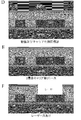
- D to F are schematic views of the cross section of the wiring board in the process from the lamination of the resin and the second-layer copper foil with a carrier to the laser drilling according to a specific example of the method for manufacturing a printed wiring board using the copper foil with a carrier of the present invention.
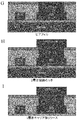
- GI are schematic views of the cross section of the wiring board in the steps from via fill formation to first layer carrier peeling, according to a specific example of the method for producing a printed wiring board using the copper foil with carrier of the present invention.
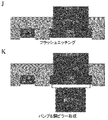
- J to K are schematic views of a cross section of a wiring board in steps from flash etching to bump / copper pillar formation according to a specific example of a method of manufacturing a printed wiring board using the carrier-attached copper foil of
- a copper foil is used as a carrier that can be used in the present invention.
- the carrier is typically provided in the form of rolled copper foil or electrolytic copper foil.
- the electrolytic copper foil is produced by electrolytic deposition of copper from a copper sulfate plating bath onto a drum of titanium or stainless steel, and the rolled copper foil is produced by repeating plastic working and heat treatment with a rolling roll.
- the copper foil material is, for example, Sn-containing copper, Ag-containing copper, copper alloy added with Cr, Zr, Mg, etc., and Corson-based added with Ni, Si, etc. Copper alloys such as copper alloys can also be used.
- a copper alloy foil is also included.
- the thickness of the carrier that can be used in the present invention is not particularly limited, but may be appropriately adjusted to a thickness suitable for serving as a carrier, for example, 12 ⁇ m or more. However, if it is too thick, the production cost becomes high, so generally it is preferably 35 ⁇ m or less. Accordingly, the thickness of the carrier is typically 12-70 ⁇ m, more typically 18-35 ⁇ m.
- An intermediate layer composed of two layers of Ni and Cr is provided on one side or both sides of the copper foil carrier.
- the Ni layer is laminated in contact with the interface with the copper foil carrier and the Cr layer is in contact with the interface with the ultrathin copper layer.
- the adhesive force between Ni and Cu is higher than the adhesive force between Cr and Cu, when the ultrathin copper layer is peeled off, it peels at the interface between the ultrathin copper layer and the Cr layer.
- the Ni layer is expected to have a barrier effect that prevents the Cu component from diffusing from the carrier into the ultrathin copper foil.
- a rust prevention layer such as a Ni plating layer on the opposite side of the copper foil carrier.
- an electrolytic copper foil it is preferable to provide an intermediate layer on the shiny surface from the viewpoint of reducing pinholes.
- the Ni layer constituting the intermediate layer can be obtained, for example, by wet plating such as electroplating, electroless plating and immersion plating, or by dry plating such as sputtering, CVD and PDV. Electroplating is preferable from the viewpoint of cost.
- the Cr layer is thin at the interface of the ultrathin copper layer, while the ultrathin copper layer does not peel off from the carrier before the lamination process to the insulating substrate, while the carrier after the lamination process to the insulating substrate Therefore, it is extremely important to obtain the property that the ultrathin copper layer can be peeled off.
- the Cr layer is present at the boundary between the carrier and the ultrathin copper layer without providing the Ni layer, the peelability is hardly improved, and when there is no Cr layer and the Ni layer and the ultrathin copper layer are directly laminated, Ni Depending on the amount of Ni in the layer, the peel strength is too strong or too weak to obtain an appropriate peel strength.
- the intermediate layer is also peeled along with the peeling of the ultrathin copper layer, that is, peeling occurs between the carrier and the intermediate layer.
- peeling occurs between the carrier and the intermediate layer.
- Such a situation can occur not only when the Cr layer is provided at the interface with the carrier, but also when the Cr amount is too large even if the Cr layer is provided at the interface with the ultrathin copper layer.
- Cu and Ni are likely to be in solid solution, and if they are in contact with each other, the adhesive force increases due to mutual diffusion and is difficult to peel off.
- Cr and Cu are less likely to dissolve and cause mutual diffusion. It is considered that the adhesive force is weak at the interface between Cr and Cu and it is easy to peel off.
- the amount of Ni in the intermediate layer is insufficient, there is only a very small amount of Cr between the carrier and the ultrathin copper layer, so that they are in close contact and are difficult to peel off.
- wet plating such as electrolytic chromate, electroplating, electroless plating and immersion plating, or sputtering, CVD and PDV This is possible by depositing a very small amount of Cr by dry plating and forming an ultrathin copper layer thereon. From the viewpoint of attaching a small amount of Cr at low cost, electrolytic chromate is preferable.
- the Ni adhesion amount contained in the intermediate layer is measured by ICP emission analysis after dissolving the sample with nitric acid having a concentration of 20% by mass, and the Cr adhesion amount and Zn adhesion amount contained in the intermediate layer are measured with a concentration of 7%. It is measured by dissolving in mass% hydrochloric acid and performing quantitative analysis by atomic absorption method.
- a plating layer containing Ni, Cr, Zn, etc. is provided on the surface of the ultrathin copper layer, after the ultrathin copper layer is peeled off, it is included in the intermediate layer by performing the above measurement on the carrier sample. Ni adhesion amount, Cr adhesion amount, and Zn adhesion amount can be measured.
- the Cr adhesion amount is preferably 10 to 50 ⁇ g / dm 2, and more preferably 15 to 40 ⁇ g / dm 2. It is preferably 10 to 20 ⁇ g / dm 2 .
- Ni deposition amount is preferably set to 2000 ⁇ 10000 ⁇ g / dm 2, more preferably to 2000 ⁇ 9000 ⁇ g / dm 2, and more preferably be 2000 ⁇ 4000 ⁇ g / dm 2.
- the intermediate layer contains a small amount of Zn.
- the occurrence of pinholes can be significantly reduced, and furthermore, it becomes easy to obtain an appropriate peel strength, which greatly contributes to quality stability.
- this is because the presence of a small amount of Zn in the intermediate layer forms an oxide film composed of Cr and Zn, and the electric conductivity of the intermediate layer is more uniform.
- the electrodeposited grains of copper when forming the ultrathin copper layer uniformly adhere to the oxide film made of Cr and Zn, and the peel strength becomes an appropriate value (the peel strength is extremely high, This is probably because the peel strength does not become extremely low.
- Zn can be present in one or both of the Ni layer and the Cr layer in the intermediate layer.
- a nickel layer containing zinc can be obtained by adding a zinc component to the plating solution and forming a nickel-zinc alloy plating when forming the Ni layer.
- a Cr layer containing zinc can be obtained by adding a zinc component to the chromate treatment solution.
- Zn diffuses in the intermediate layer, it is generally detected in both the Ni layer and the Cr layer.
- Zn is preferably present in the Cr layer because an oxide film made of Cr and Zn is easily formed.
- the adhesion amount of Zn in the intermediate layer is too small because the effect is limited, it should be 1 [mu] g / dm 2 or more, preferably set to 5 [mu] g / dm 2 or more.
- the amount of Zn deposited on the intermediate layer is too large, the peel strength becomes excessive, so it should be 70 ⁇ g / dm 2 or less, preferably 30 ⁇ g / dm 2 or less, and 20 ⁇ g / dm 2 or less. Is more preferable.
- the value of the mass ratio of Zn to Cr (Zn adhesion amount / Cr adhesion amount) is preferably in the range of 0.01 to 5.00, more preferably in the range of 0.1 to 1.0. 0.2 to 0.8 is preferable. This is because the generation of pinholes and the peeling characteristics of the ultrathin copper foil are improved by setting the amount of Zn to Cr within the above range.
- Ultra-thin copper layer An ultrathin copper layer is provided on the intermediate layer.
- the ultra-thin copper layer can be formed by electroplating using an electrolytic bath such as copper sulfate, copper pyrophosphate, copper sulfamate, copper cyanide, etc., and is used in general electrolytic copper foil with high current density. Since a copper foil can be formed, a copper sulfate bath is preferable.
- the thickness of the ultrathin copper layer is not particularly limited, but is generally thinner than the carrier, for example, 12 ⁇ m or less. Typically 0.5 to 12 ⁇ m, more typically 2 to 5 ⁇ m.
- a roughening treatment layer may be provided on the surface of the ultrathin copper layer by performing a roughening treatment, for example, in order to improve the adhesion to the insulating substrate.
- the roughening treatment can be performed, for example, by forming roughened particles with copper or a copper alloy.
- the roughening process may be fine.
- the roughening treatment layer is a layer made of any single element selected from the group consisting of copper, nickel, cobalt, phosphorus, tungsten, arsenic, molybdenum, chromium and zinc, or an alloy containing one or more of them. Also good.
- a roughening treatment can be performed in which secondary particles or tertiary particles are further formed of nickel, cobalt, copper, zinc alone or an alloy.
- a heat-resistant layer or a rust-preventing layer may be formed of nickel, cobalt, copper, zinc alone or an alloy, and the surface thereof may be further subjected to a treatment such as a chromate treatment or a silane coupling treatment.
- a heat-resistant layer or a rust-preventing layer may be formed from nickel, cobalt, copper, zinc alone or an alloy without roughening, and the surface may be subjected to a treatment such as chromate treatment or silane coupling treatment. Good.
- one or more layers selected from the group consisting of a heat-resistant layer, a rust-preventing layer, a chromate treatment layer, and a silane coupling treatment layer may be formed on the surface of the roughening treatment layer.
- One or more layers selected from the group consisting of a heat-resistant layer, a rust prevention layer, a chromate treatment layer, and a silane coupling treatment layer may be formed on the surface.
- the above-mentioned heat-resistant layer, rust prevention layer, chromate treatment layer, and silane coupling treatment layer may each be formed of a plurality of layers such as 2 layers or more and 3 layers or more.
- a roughening treatment layer may be provided on the ultrathin copper layer, and a heat resistant layer and a rust prevention layer may be provided on the roughening treatment layer.
- a chromate treatment layer may be provided on the layer and the anticorrosion layer, and a silane coupling treatment layer may be provided on the chromate treatment layer.
- the heat-resistant layer and the rust-proof layer known heat-resistant layers and rust-proof layers can be used.
- the heat-resistant layer and / or the anticorrosive layer is a group of nickel, zinc, tin, cobalt, molybdenum, copper, tungsten, phosphorus, arsenic, chromium, vanadium, titanium, aluminum, gold, silver, platinum group elements, iron, tantalum
- it may be a metal layer or an alloy layer made of one or more elements selected from the group consisting of iron, tantalum and the like.
- the heat-resistant layer and / or rust preventive layer is a group of nickel, zinc, tin, cobalt, molybdenum, copper, tungsten, phosphorus, arsenic, chromium, vanadium, titanium, aluminum, gold, silver, platinum group elements, iron, and tantalum.
- An oxide, nitride, or silicide containing one or more elements selected from the above may be included.
- the heat-resistant layer and / or the rust preventive layer may be a layer containing a nickel-zinc alloy.
- the heat-resistant layer and / or the rust preventive layer may be a nickel-zinc alloy layer.
- the nickel-zinc alloy layer may contain 50 wt% to 99 wt% nickel and 50 wt% to 1 wt% zinc, excluding inevitable impurities.
- the total adhesion amount of zinc and nickel in the nickel-zinc alloy layer may be 5 to 1000 mg / m 2 , preferably 10 to 500 mg / m 2 , preferably 20 to 100 mg / m 2 .
- the amount of nickel deposited on the layer containing the nickel-zinc alloy or the nickel-zinc alloy layer is preferably 0.5 mg / m 2 to 500 mg / m 2 , and 1 mg / m 2 to 50 mg / m 2 . More preferably.
- the heat-resistant layer and / or rust prevention layer is a layer containing a nickel-zinc alloy, the interface between the copper foil and the resin substrate is eroded by the desmear liquid when the inner wall of a through hole or via hole comes into contact with the desmear liquid. It is difficult to improve the adhesion between the copper foil and the resin substrate.
- the heat-resistant layer and / or the rust preventive layer has a nickel or nickel alloy layer with an adhesion amount of 1 mg / m 2 to 100 mg / m 2 , preferably 5 mg / m 2 to 50 mg / m 2 , and an adhesion amount of 1 mg / m 2.
- a tin layer of ⁇ 80 mg / m 2 , preferably 5 mg / m 2 ⁇ 40 mg / m 2 may be sequentially laminated.
- the nickel alloy layer may be nickel-molybdenum, nickel-zinc, nickel-molybdenum-cobalt. You may be comprised by any one of these.
- the heat-resistant layer and / or rust-preventing layer preferably has a total adhesion amount of nickel or nickel alloy and tin of 2 mg / m 2 to 150 mg / m 2 and 10 mg / m 2 to 70 mg / m 2 . It is more preferable.
- silane coupling agent for the silane coupling agent used for a silane coupling process, for example, using an amino-type silane coupling agent or an epoxy-type silane coupling agent, a mercapto-type silane coupling agent.
- Silane coupling agents include vinyltrimethoxysilane, vinylphenyltrimethoxylane, ⁇ -methacryloxypropyltrimethoxysilane, ⁇ -glycidoxypropyltrimethoxysilane, 4-glycidylbutyltrimethoxysilane, and ⁇ -aminopropyl.
- Triethoxysilane N- ⁇ (aminoethyl) ⁇ -aminopropyltrimethoxysilane, N-3- (4- (3-aminopropoxy) ptoxy) propyl-3-aminopropyltrimethoxysilane, imidazole silane, triazine silane, ⁇ -mercaptopropyltrimethoxysilane or the like may be used.
- the silane coupling treatment layer may be formed using a silane coupling agent such as epoxy silane, amino silane, methacryloxy silane, mercapto silane, or the like.
- a silane coupling agent such as epoxy silane, amino silane, methacryloxy silane, mercapto silane, or the like.
- you may use 2 or more types of such silane coupling agents in mixture.
- it is preferable to form using an amino-type silane coupling agent or an epoxy-type silane coupling agent.
- the amino silane coupling agent referred to here is N- (2-aminoethyl) -3-aminopropyltrimethoxysilane, 3- (N-styrylmethyl-2-aminoethylamino) propyltrimethoxysilane, 3- Aminopropyltriethoxysilane, bis (2-hydroxyethyl) -3-aminopropyltriethoxysilane, aminopropyltrimethoxysilane, N-methylaminopropyltrimethoxysilane, N-phenylaminopropyltrimethoxysilane, N- (3 -Acryloxy-2-hydroxypropyl) -3-aminopropyltriethoxysilane, 4-aminobutyltriethoxysilane, (aminoethylaminomethyl) phenethyltrimethoxysilane, N- (2-aminoethyl-3-aminopropyl
- the silane coupling treatment layer is 0.05 mg / m 2 to 200 mg / m 2 , preferably 0.15 mg / m 2 to 20 mg / m 2 , preferably 0.3 mg / m 2 to 2.0 mg in terms of silicon atoms. / M 2 is desirable. In the case of the above-mentioned range, the adhesiveness between the base resin and the surface-treated copper foil can be further improved.
- the carrier-attached copper foil includes a resin layer on the ultrathin copper layer, the roughened layer, the heat-resistant layer, the rust-proof layer, the chromate-treated layer, or the silane coupling-treated layer. May be.
- the resin layer may be an insulating resin layer.
- the resin layer may be an adhesive or an insulating resin layer in a semi-cured state (B stage state) for bonding.
- the semi-cured state (B stage state) is a state in which there is no sticky feeling even if the surface is touched with a finger, the insulating resin layer can be stacked and stored, and a curing reaction occurs when subjected to heat treatment. Including that.
- the resin layer may include a thermosetting resin or may include a thermoplastic resin.
- the type is not particularly limited.
- the resin layer may be a resin layer containing a block copolymerized polyimide resin layer or a resin layer containing a block copolymerized polyimide resin and a polymaleimide compound.
- the epoxy resin has two or more epoxy groups in the molecule and can be used without any problem as long as it can be used for electric / electronic materials.
- the epoxy resin is preferably an epoxy resin epoxidized using a compound having two or more glycidyl groups in the molecule.
- Bisphenol A type epoxy resin bisphenol F type epoxy resin, bisphenol S type epoxy resin, bisphenol AD type epoxy resin, novolac type epoxy resin, cresol novolac type epoxy resin, alicyclic epoxy resin, brominated epoxy resin, glycidylamine Type epoxy resin, triglycidyl isocyanurate, glycidyl amine compound such as N, N-diglycidyl aniline, glycidyl ester compound such as tetrahydrophthalic acid diglycidyl ester, phosphorus-containing epoxy resin, biphenyl type epoxy resin, biphenyl novolac type epoxy resin, One or two or more selected from the group of trishydroxyphenylmethane type epoxy resin and tetraphenylethane type epoxy resin can be used, or the epoxy Resin hydrogenated products and halogenated products can be used.
- the anhydride of the polyvalent carboxylic acid is preferably a component that contributes as a curing agent for the epoxy resin.
- the anhydride of the polyvalent carboxylic acid is phthalic anhydride, maleic anhydride, trimellitic anhydride, pyromellitic anhydride, tetrahydroxyphthalic anhydride, hexahydroxyphthalic anhydride, methylhexahydroxyphthalic anhydride, nadine. Acid and methyl nadic acid are preferred.
- the resin composition for forming the resin layer may contain an anhydride of polyvalent carboxylic acid, a phenoxy resin, and an epoxy resin.
- the acid anhydride is preferably contained in an amount of 0.01 mol to 0.5 mol with respect to 1 mol of the hydroxyl group contained in the phenoxy resin.
- the phenoxy resin one synthesized by a reaction between bisphenol and a divalent epoxy resin can be used.
- the content of the phenoxy resin may be 3 to 30 parts by weight when the total amount of the resin composition is 100 parts by weight.
- the epoxy resin may be an epoxy resin epoxidized with a compound having two or more glycidyl groups in the molecule.
- the resin composition can be obtained by reacting a polycarboxylic acid anhydride with a phenoxy resin, ring-opening addition of the polyvalent carboxylic acid to the hydroxyl group of the phenoxy resin, and then adding an epoxy resin. it can.
- bisphenol examples include bisphenol A, bisphenol F, bisphenol S, tetrabromobisphenol A, 4,4′-dihydroxybiphenyl, HCA (9,10-Dihydro-9-Oxa-10-Phosphophenanthrene-10-Oxide), hydroquinone, naphthoquinone, etc.
- Bisphenol obtained as an adduct with quinones can be used.
- the thermoplastic resin may be a thermoplastic resin having a functional group other than an alcoholic hydroxyl group polymerizable with an epoxy resin.
- the composition of the resin layer contains 50 to 90% by weight of an epoxy resin, 5 to 20% by weight of a polyvinyl acetal resin, and 0.1 to 20% by weight of a urethane resin with respect to the total amount of the resin components. 40% by weight may be a rubber-modified epoxy resin.
- the polyvinyl acetal resin may have a functional group polymerizable with an epoxy resin or a maleimide compound other than an acid group and a hydroxyl group.
- the resin layer is composed of 20 to 80 parts by weight of an epoxy resin (including a curing agent), 20 to 80 parts by weight of an aromatic polyamide resin polymer soluble in a solvent, and a curing that is added in an appropriate amount as necessary. It may be formed using a resin composition made of an accelerator.
- the resin layer is 5 to 80 parts by weight of an epoxy resin (including a curing agent), 20 to 95 parts by weight of an aromatic polyamide resin polymer soluble in a solvent, and a curing that is added in an appropriate amount as necessary. It may be formed using a resin composition made of an accelerator.
- the aromatic polyamide resin polymer used for the composition of the resin composition used for forming the resin layer may be obtained by reacting an aromatic polyamide with a rubber resin.
- the resin layer may contain a dielectric filler.
- the resin layer may contain a skeleton material.
- examples of the aromatic polyamide resin polymer include those obtained by reacting an aromatic polyamide resin and a rubber resin.
- the aromatic polyamide resin is synthesized by condensation polymerization of an aromatic diamine and a dicarboxylic acid.
- aromatic diamine As the aromatic diamine at this time, 4,4′-diaminodiphenylmethane, 3,3′-diaminodiphenylsulfone, m-xylenediamine, 3,3′-oxydianiline and the like are used.
- dicarboxylic acid phthalic acid, isophthalic acid, terephthalic acid, fumaric acid or the like is used.
- the rubbery resin to be reacted with the aromatic polyamide resin is described as a concept including natural rubber and synthetic rubber.
- the latter synthetic rubber includes styrene-butadiene rubber, butadiene rubber, butyl rubber, ethylene-propylene. There is rubber.
- a synthetic rubber having heat resistance such as nitrile rubber, chloroprene rubber, silicon rubber, urethane rubber or the like. Since these rubber resins react with an aromatic polyamide resin to produce a copolymer, it is desirable to have various functional groups at both ends. In particular, it is useful to use CTBN (carboxy group-terminated butadiene nitrile).
- the aromatic polyamide resin and rubber resin that constitute the aromatic polyamide resin polymer are preferably used in a blend of 25 wt% to 75 wt% of the aromatic polyamide resin and the remaining rubber resin.
- the aromatic polyamide resin is less than 25 wt%, the abundance ratio of the rubber component is too high and the heat resistance is inferior.
- the aromatic polyamide resin exceeds 75 wt%, the abundance ratio of the aromatic polyamide resin is too large to be cured. Later hardness becomes too high and becomes brittle.
- This aromatic polyamide resin polymer is used for the purpose of not being damaged by under-etching by an etchant when etching a copper foil after being processed into a copper-clad laminate.
- This aromatic polyamide resin polymer is required to be soluble in a solvent.
- This aromatic polyamide resin polymer is used in a blending ratio of 20 to 80 parts by weight.
- the amount of the aromatic polyamide resin polymer is less than 20 parts by weight, it becomes too brittle under general press conditions for producing a copper clad laminate, and becomes microcracked easily on the substrate surface.
- the curing accelerator to be added in an appropriate amount as needed includes tertiary amines, imidazoles, urea-based curing accelerators, and the like.
- the mixing ratio of the curing accelerator is not particularly limited. This is because the curing accelerator may be arbitrarily selected by the manufacturer in consideration of production conditions in the process of producing the copper-clad laminate.
- the resin composition for forming the resin layer is prepared by dissolving three types of epoxy resins, a bisphenol A type epoxy resin, a cresol novolac type epoxy resin, and a brominated bisphenol A type epoxy resin, in a solvent, and a curing agent and finely pulverizing them. It may be a resin composition to which a reaction catalyst such as silica or antimony trioxide is added. The curing agent at this time is the same as described above. This resin composition also shows good adhesion between the copper foil and the base resin.
- the resin composition for forming the resin layer is polyphenylene ether resin, 2,2-bis (4-cyanatophenyl) propane, phosphorus-containing phenol compound, manganese naphthenate, 2,2-bis (4-glycidylphenyl) It may be a polyphenylene ether-cyanate resin composition in which propane is dissolved in a solvent. This resin composition also shows good adhesion between the copper foil and the base resin.
- the resin composition for forming the resin layer may be a siloxane-modified polyamideimide resin composition or a siloxane-modified polyamideimide resin composition in which a cresol novolac type epoxy resin is dissolved in a solvent. This resin composition also shows good adhesion between the copper foil and the base resin.
- the dielectric (dielectric filler) includes a composite oxide having a perovskite structure such as BaTiO3, SrTiO3, Pb (Zr-Ti) O3 (commonly called PZT), PbLaTiO3 / PbLaZrO (commonly known as PLZT), SrBi2Ta2O9 (commonly known as SBT), and the like. Dielectric powder is used.
- the dielectric (dielectric filler) may be in powder form.
- the powder characteristics of the dielectric (dielectric filler) are as follows. First, the particle size is 0.01 ⁇ m to 3.0 ⁇ m, preferably 0.02 ⁇ m to 2.0 ⁇ m. Must be in range.
- the particle size referred to here is indirect in which the average particle size is estimated from the measured values of the laser diffraction scattering type particle size distribution measurement method and the BET method because the particles form a certain secondary aggregation state.
- the accuracy is inferior in measurement, and it refers to the average particle diameter obtained by directly observing a dielectric (dielectric filler) with a scanning electron microscope (SEM) and image analysis of the SEM image. It is. In this specification, the particle size at this time is indicated as DIA.
- the image analysis of the dielectric (dielectric filler) powder observed using a scanning electron microscope (SEM) in this specification is performed using an IP-1000PC manufactured by Asahi Engineering Co., Ltd. Circular particle analysis was performed with a threshold value of 10 and an overlapping degree of 20, and the average particle diameter DIA was obtained.
- the volume cumulative particle diameter D50 by the laser diffraction scattering particle size distribution measurement method is 0.2 ⁇ m to 2.0 ⁇ m, and the volume cumulative particle diameter D50 and the average particle diameter DIA obtained by image analysis are used to obtain D50 / It is required to be a dielectric powder having a substantially spherical perovskite structure with a cohesion value represented by DIA of 4.5 or less.
- the volume cumulative particle size D50 by the laser diffraction scattering type particle size distribution measurement method is a particle size at 50% weight cumulative obtained by using the laser diffraction scattering type particle size distribution measurement method, and the value of this volume cumulative particle size D50.
- the dielectric layer of the double-sided copper-clad laminate used to form the built-in capacitor layer is usually 10 ⁇ m to 25 ⁇ m thick, and 2.0 ⁇ m to uniformly disperse the dielectric filler therein. Is the upper limit.
- the volume cumulative particle size D50 is measured by mixing and dispersing a dielectric (dielectric filler) powder in methyl ethyl ketone, and then dispersing this solution into a laser diffraction scattering type particle size distribution measuring device “Micro” Trac ”HRA” 9320-X100 (manufactured by Nikkiso Co., Ltd.). ) And then measured.
- the concept of cohesion is used here, but it is adopted for the following reasons. That is, the value of the volume cumulative particle size D50 obtained by using the laser diffraction / scattering particle size distribution measurement method is considered not to be a direct observation of each individual particle size. This is because the powder particles constituting most of the dielectric powder are not so-called monodispersed powders in which individual particles are completely separated, but are in a state where a plurality of powder particles are aggregated and aggregated. This is because the laser diffraction / scattering particle size distribution measurement method regards the aggregated particles as one particle (aggregated particle) and calculates the volume cumulative particle size.
- the average particle diameter DIA obtained by image processing the observation image of the dielectric powder observed using the scanning electron microscope is obtained directly from the SEM observation image, the primary particles are surely obtained.
- the presence of the agglomerated state of the particles is not reflected at all.
- the present inventors calculated the value calculated by D50 / DIA using the volume cumulative particle diameter D50 of the laser diffraction scattering particle size distribution measurement method and the average particle diameter DIA obtained by image analysis. Is regarded as the degree of cohesion. That is, assuming that the values of D50 and DIA can be measured with the same accuracy in the same lot of copper powder, considering the above-mentioned theory, the value of D50 that reflects the presence of an agglomerated state is DIA. It is considered that the value is larger than the value of.
- the value of D50 approaches the value of DIA as much as possible if the state of aggregation of the dielectric (dielectric filler) powder is completely eliminated.
- the value of D50 / DIA as the degree of aggregation is It approaches 1 It can be said that it is a monodispersed powder in which the agglomeration state of the powder is completely lost when the aggregation degree becomes 1.
- the degree of aggregation may be less than 1. Theoretically, in the case of a true sphere, it does not become a value less than 1, but in reality, it seems that a cohesion value of less than 1 is obtained because the powder is not a true sphere. is there.
- the degree of aggregation of the dielectric (dielectric filler) powder is preferably 4.5 or less. If this degree of aggregation exceeds 4.5, the level of aggregation between the powder particles of the dielectric filler becomes too high, and uniform mixing with the above-described resin composition becomes difficult.
- a fixed aggregation state is inevitably formed even if any production method such as an alkoxide method, a hydrothermal synthesis method, or an oxalate method is employed.
- Dielectric filler powder that does not satisfy the degree of aggregation can be generated.
- the hydrothermal synthesis method which is a wet method the formation of an aggregated state tends to occur. Therefore, the aggregated state of the dielectric filler powder can be set within the above-described aggregation degree range by performing a pulverization process for separating the agglomerated powder into one granular particle. is there.
- a pulverizer can be used.
- the specific surface area of the dielectric particles (dielectric filler) is required to be small and smooth. Therefore, even if granulation is possible, it should not be a granulation technique that damages the surface of the granule during granulation and increases its specific surface area.
- the inventors of the present invention conducted extensive research and found that the two methods were effective. What is common to these two methods is that the powder particles of the dielectric (dielectric filler) are agglomerated while minimizing the contact of the powder with the inner wall of the device, the stirring blade, the grinding media, etc.
- This is a method capable of sufficiently pulverizing particles by causing the particles to collide with each other. That is, contact with parts such as the inner wall of the apparatus, stirring blades, and grinding media damages the surface of the powder, increases the surface roughness, and deteriorates the sphericity, thereby preventing this. .
- the dielectric (dielectric filler) powder in the aggregated state is pulverized using a jet mill.
- Jet mill refers to the use of a high-speed air current to place dielectric (dielectric filler) powder in this air current, and the particles collide with each other in this high-speed air current to break up the particles. Is done.
- a slurry in which a dielectric (dielectric filler) powder in an agglomerated state is dispersed in a solvent that does not destroy the stoichiometry is pulverized using a fluid mill using centrifugal force.
- the slurry is allowed to flow at a high speed so as to draw a circumferential trajectory. And then pulverize.
- the dielectric (dielectric filler) powder which finished the granulation work is obtained by washing, filtering, and drying the slurry after the granulation work.
- the degree of aggregation can be adjusted and the powder surface of the dielectric filler powder can be smoothed.
- the above-described resin composition and dielectric (dielectric filler) are mixed to obtain a dielectric (dielectric filler) -containing resin for forming a built-in capacitor layer of a printed wiring board.
- resin which can be used for the said resin layer can be mentioned as resin used for the resin composition for mixing with a dielectric material (dielectric filler).
- the blending ratio of the resin composition and the dielectric (dielectric filler) is 75 wt% to 85 wt% in the content of the dielectric (dielectric filler), and the remaining resin composition.
- the content of the dielectric (dielectric filler) is less than 75 wt%, the relative permittivity of 20 currently required in the market cannot be satisfied, and the content of the dielectric (dielectric filler) exceeds 85 wt%.
- the resin composition content is less than 15 wt%, the adhesiveness between the dielectric (dielectric filler) -containing resin and the copper foil laminated thereon is impaired, and the required characteristics for manufacturing a printed wiring board are satisfied. This makes it difficult to produce a copper-clad laminate.
- the resin layer containing the dielectric (dielectric filler) may be formed using a resin composition containing a dielectric (dielectric filler), an epoxy resin, an active ester resin, a polyvinyl acetal resin, and a curing accelerator. Good. Further, the resin layer containing the dielectric (dielectric filler) is 25 parts by weight of epoxy resin when the weight of the resin composition containing epoxy resin, active ester resin, polyvinyl acetal resin, and curing accelerator is 100 parts by weight. It may be formed using a resin composition containing ⁇ 60 parts by weight and a dielectric (dielectric filler).
- the resin layer containing the dielectric material (dielectric filler) is 28 weight parts of the active ester resin when the weight of the resin composition containing the epoxy resin, the active ester resin, the polyvinyl acetal resin, and the curing accelerator is 100 parts by weight. It may be formed using a resin composition containing from 60 parts by weight to 60 parts by weight and a dielectric (dielectric filler). Further, the resin layer containing the dielectric (dielectric filler) has an epoxy resin and an active ester resin when the weight of the resin composition containing an epoxy resin, an active ester resin, a polyvinyl acetal resin, and a curing accelerator is 100 parts by weight.
- the resin layer containing the dielectric (dielectric filler) has 1 weight of polyvinyl acetal resin when the weight of the resin composition containing epoxy resin, active ester resin, polyvinyl acetal resin, and curing accelerator is 100 parts by weight. It may be formed using a resin composition containing from 20 to 20 parts by weight and a dielectric (dielectric filler). Further, the resin layer containing the dielectric (dielectric filler) has a curing accelerator of 0.00 when the weight of the resin composition containing epoxy resin, active ester resin, polyvinyl acetal resin, and curing accelerator is 100 parts by weight.
- the resin layer containing the dielectric (dielectric filler) has an epoxy resin, an active ester resin, and a polyvinyl acetal constituting the resin composition when the weight of the resin composition constituting the resin layer is 100 parts by weight. It may be formed using a resin composition in which the total amount of each component of the resin and the curing accelerator is 70 parts by weight or more and a dielectric (dielectric filler).
- the resin layer containing a dielectric contains a dielectric (dielectric filler) in a range of 65 wt% to 85 wt% when the weight of the resin containing the dielectric (dielectric filler) is 100 wt%.
- the epoxy resin, active ester resin, polyvinyl acetal resin and curing accelerator include known epoxy resins, active ester resins, polyvinyl acetal resins and curing accelerators, or the epoxy resins, active ester resins and polyvinyl acetals described in the present specification. Resins and cure accelerators can be used.
- the resin layer containing the dielectric (dielectric filler) preferably has a resin flow of less than 1% when measured according to MIL-P-13949G in the MIL standard.
- a hardening accelerator and an epoxy resin a well-known thing or the hardening accelerator and epoxy resin as described in this-application specification can be used.
- a hardening accelerator a well-known imidazole compound or the imidazole compound as described in this-application specification can be used.
- this dielectric dielectric filler
- barium titanate among complex oxides having a perovskite structure in consideration of manufacturing accuracy as a powder at the present stage.
- the dielectric (dielectric filler) at this time either calcined barium titanate or uncalcined barium titanate can be used. In order to obtain a high dielectric constant, it is preferable to use calcined barium titanate, but it may be selectively used according to the design quality of the printed wiring board product.
- the dielectric filler of barium titanate has a cubic crystal structure.
- the crystal structure of barium titanate includes cubic and tetragonal crystals, but the cubic barium titanate dielectric (dielectric filler) has a tetragonal structure only.
- the value of the dielectric constant of the finally obtained dielectric layer is stabilized as compared with the case where a barium acid dielectric (dielectric filler) is used. Therefore, it can be said that it is necessary to use barium titanate powder having both a cubic crystal structure and a tetragonal crystal structure.
- the resin layer containing the dielectric for forming the capacitor circuit layer having a low dielectric loss tangent is improved by improving the adhesion between the inner layer circuit surface of the inner layer core material and the resin layer containing the dielectric.
- the copper foil with a carrier which has can be provided.
- the resin layer is a cured resin layer (the “cured resin layer” means a cured resin layer) and a half in order from the copper foil side (that is, the ultrathin copper layer side of the copper foil with carrier).
- the resin layer which formed the cured resin layer sequentially may be sufficient.
- the cured resin layer may be composed of a resin component of any one of a polyimide resin, a polyamideimide resin, and a composite resin having a thermal expansion coefficient of 0 ppm / ° C. to 25 ppm / ° C.
- a semi-cured resin layer having a coefficient of thermal expansion after curing of 0 ppm / ° C. to 50 ppm / ° C. may be provided on the cured resin layer.
- the thermal expansion coefficient of the entire resin layer after the cured resin layer and the semi-cured resin layer are cured may be 40 ppm / ° C. or less.
- the cured resin layer may have a glass transition temperature of 300 ° C. or higher.
- the semi-cured resin layer may be formed using a maleimide resin, and the maleimide resin may be an aromatic maleimide resin having two or more maleimide groups in the molecule.
- the maleimide resin may be a polymerized adduct obtained by polymerizing an aromatic maleimide resin having two or more maleimide groups in the molecule and an aromatic polyamine. Further, the semi-cured resin layer may contain 20 to 70 parts by weight of a maleimide resin when the semi-cured resin layer is 100 parts by weight.
- the resin composition for forming the semi-cured resin layer preferably contains a maleimide resin, an epoxy resin, and a linear polymer having a crosslinkable functional group as an essential component.
- the maleimide resin may be a polymerization adduct obtained by polymerizing an aromatic maleimide resin and an aromatic polyamine.
- cyanoester resin and epoxy resin which have reactivity with a maleimide-type resin as needed to a semi-hardened resin layer.
- epoxy resin a known epoxy resin or an epoxy resin described in the present specification can be used.
- the linear polymer having a crosslinkable functional group preferably has a functional group that contributes to the curing reaction of an epoxy resin such as a hydroxyl group or a carboxyl group.
- the linear polymer having a crosslinkable functional group is preferably soluble in an organic solvent having a boiling point of 50 ° C. to 200 ° C.
- Specific examples of the linear polymer having a functional group mentioned here include polyvinyl acetal resin, phenoxy resin, polyethersulfone resin, polyamideimide resin and the like.
- the linear polymer having a crosslinkable functional group is preferably used in a blending ratio of 3 to 30 parts by weight when the resin composition is 100 parts by weight. When the epoxy resin is less than 3 parts by weight, the resin flow may increase.
- maleimide resins examples include 4,4′-diphenylmethane bismaleimide, polyphenylmethane maleimide, m-phenylene bismaleimide, bisphenol A diphenyl ether bismaleimide, 3,3′-dimethyl-5,5′-diethyl-4. , 4'-diphenylmethane bismaleimide, 4-methyl-1,3-phenylene bismaleimide, 4,4'-diphenyl ether bismaleimide, 4,4'-diphenylsulfone bismaleimide, 1,3-bis (3-maleimidophenoxy) Benzene, 1,3-bis (4-maleimidophenoxy) benzene and the like can be used.
- the content of the maleimide resin is less than 20 parts by weight, the effect of reducing the thermal expansion coefficient of the semi-cured resin layer after curing may not be obtained.
- the content of the maleimide resin exceeds 70 parts by weight, the semi-cured resin layer may become a brittle resin layer when cured, and the resin layer may be easily cracked. The reliability as a layer may be reduced.
- examples of the aromatic polyamine include m-phenylenediamine and p-phenylenediamine.
- epoxy resin curing agent When an epoxy resin curing agent is required, amines such as dicyandiamide, imidazoles and aromatic amines, phenols such as bisphenol A and brominated bisphenol A, novolacs such as phenol novolac resin and cresol novolac resin Acid anhydrides such as phthalic anhydride are used. Since the addition amount of the epoxy resin curing agent with respect to the epoxy resin at this time is naturally derived from the respective equivalents, no special addition amount limitation is performed.
- amines such as dicyandiamide, imidazoles and aromatic amines
- phenols such as bisphenol A and brominated bisphenol A
- novolacs such as phenol novolac resin and cresol novolac resin
- Acid anhydrides such as phthalic anhydride
- the said cured resin layer is a polymeric polymer layer which has hardened
- the polymer layer is preferably made of a resin having a glass transition temperature of 150 ° C. or higher so that it can withstand the solder mounting process.
- the polymer polymer layer is preferably made of one or a mixture of two or more of a polyamide resin, a polyether sulfone resin, an aramid resin, a phenoxy resin, a polyimide resin, a polyvinyl acetal resin, and a polyamideimide resin.
- the thickness of the polymer layer is preferably 3 ⁇ m to 10 ⁇ m. Moreover, it is preferable that the said high polymer layer contains any 1 type, or 2 or more types of an epoxy resin, a maleimide resin, a phenol resin, and a urethane resin.
- the semi-cured resin layer is preferably composed of an epoxy resin composition having a thickness of 10 ⁇ m to 50 ⁇ m.
- the epoxy resin composition preferably contains the following components A to E.
- Component A An epoxy resin having one or more selected from the group consisting of a bisphenol A type epoxy resin, a bisphenol F type epoxy resin, and a bisphenol AD type epoxy resin that have an epoxy equivalent of 200 or less and are liquid at room temperature.
- B component High heat-resistant epoxy resin.
- Component C Phosphorus-containing flame-retardant resin, which is any one of phosphorus-containing epoxy resin and phosphazene-based resin, or a mixture of these.
- Component D A rubber-modified polyamideimide resin modified with a liquid rubber component having a property of being soluble in a solvent having a boiling point in the range of 50 ° C. to 200 ° C.
- E component Resin curing agent.
- the component A is an epoxy resin composed of one or more selected from the group consisting of a bisphenol A type epoxy resin, a bisphenol F type epoxy resin, and a bisphenol AD type epoxy resin that have an epoxy equivalent of 200 or less and are liquid at room temperature.
- the bisphenol-based epoxy resin is selectively used because it has good compatibility with the D component (rubber-modified polyamideimide resin) described later, and it is easy to impart appropriate flexibility to the resin film in a semi-cured state. It is. If the epoxy equivalent exceeds 200, the resin becomes semi-solid at room temperature, and the flexibility in the semi-cured state decreases, which is not preferable.
- 1 type may be used independently or 2 or more types may be used in mixture. In addition, when two or more kinds are mixed and used, there is no particular limitation with respect to the mixing ratio.
- This epoxy resin is preferably used in a blending ratio of 3 to 30 parts by weight, based on 100 parts by weight of the epoxy resin composition constituting the semi-cured resin layer.
- the epoxy resin is less than 3 parts by weight, the thermosetting property is not sufficiently exhibited, and the function as a binder with the inner layer flexible printed wiring board and the adhesiveness with the copper foil as the resin-coated copper foil are sufficient. Can't be done.
- the amount exceeds 30 parts by weight the viscosity of the resin varnish increases from the balance with other resin components, and when the resin-coated copper foil is produced, the resin film with a uniform thickness is formed on the copper foil surface. Formation becomes difficult.
- D component rubber-modified polyamideimide resin
- the B component is a “high heat resistant epoxy resin” having a high so-called glass transition point Tg.
- the “high heat-resistant epoxy resin” referred to here is preferably a polyfunctional epoxy resin such as a novolac-type epoxy resin, a cresol novolac-type epoxy resin, a phenol novolac-type epoxy resin, or a naphthalene-type epoxy resin.
- the component B is preferably used in the range of 3 to 30 parts by weight, based on 100 parts by weight of the epoxy resin composition constituting the semi-cured resin layer. When the component B is less than 3 parts by weight, it is not preferable because the Tg of the resin composition tends to be insufficient.
- the component B exceeds 30 parts by weight, the cured resin becomes brittle and flexibility is impaired, which is not preferable for flexible printed wiring board applications. More preferably, the B component is used in the range of 10 to 20 parts by weight, so that both high Tg of the resin composition and good flexibility of the cured resin can be stably achieved.
- the component C is a so-called halogen-free flame-retardant resin, and a phosphorus-containing flame-retardant resin, which is any one of a phosphorus-containing epoxy resin and a phosphazene-based resin, or a mixture of these is used.
- the phosphorus-containing epoxy resin is a general term for epoxy resins containing phosphorus in an epoxy skeleton. When the phosphorus atom content of the epoxy resin composition constituting the semi-cured resin layer is 100% by weight of the epoxy resin composition, 0.5% by weight to 3.0% by weight of phosphorus atoms derived from component C is obtained. Any phosphorus-containing epoxy resin that can be in the range of% by weight can be used.
- a phosphorus-containing epoxy resin that is a 9,10-dihydro-9-oxa-10-phosphaphenanthrene-10-oxide derivative having two or more epoxy groups in the molecule is used.
- the structural formula of 9,10-dihydro-9-oxa-10-phosphaphenanthrene-10-oxide is shown below.
- a compound having the structural formula shown in Chemical Formula 2 is shown.
- the use of a compound having the structural formula shown in Chemical Formula 2 is preferable because the resin quality is more stable in a semi-cured state, and at the same time, the flame retardant effect is enhanced.
- the phosphorus-containing epoxy resin of the C component a compound having a structural formula shown in Chemical Formula 3 shown below is also preferable.
- the resin quality is excellent in the semi-cured state, and high flame retardancy can be imparted at the same time, which is preferable.
- the C component phosphorus-containing epoxy resin a compound having the structural formula shown in Chemical Formula 4 below is also preferable. Like the phosphorus-containing epoxy resin shown in Chemical Formula 2 and Chemical Formula 3, it is preferable because it is excellent in the stability of the resin quality in a semi-cured state and at the same time imparting high flame resistance.
- the epoxy resin obtained as a derivative from 9,10-dihydro-9-oxa-10-phosphaphenanthrene-10-oxide is converted to 9,10-dihydro-9-oxa-10-phosphaphenanthrene-10-oxide.
- a compound represented by the following chemical formula 5 (HCA-NQ) or chemical formula 6 (HCA-HQ) an epoxy resin is reacted with the OH group portion to obtain a phosphorus-containing flame retardant resin.
- the resin composition in the case of using a phosphorus-containing epoxy resin as the phosphorus-containing flame retardant resin is not limited to two or more types of phosphorus-containing epoxy resins, even if one kind of phosphorus-containing epoxy resin is used alone. You may mix and use.
- the phosphorus atom derived from the C component is 0.5% by weight.
- the addition amount is preferably determined so as to be in the range of from% to 3.0% by weight.
- the phosphorus-containing epoxy resin has different amounts of phosphorus atoms contained in the epoxy skeleton depending on the type. Therefore, as described above, the phosphorus atom content can be designed with priority over the added amount of the C component.
- the phosphazene resin is a resin containing phosphazene having a double bond having phosphorus and nitrogen as constituent elements.
- the phosphazene resin can dramatically improve the flame retardancy due to the synergistic effect of nitrogen and phosphorus in the molecule.
- unlike 9,10-dihydro-9-oxa-10-phosphaphenanthrene-10-oxide derivatives they exist stably in the resin, and an effect of preventing the occurrence of migration can be obtained.
- the resin composition in the case of using a phosphazene resin as the phosphorus-containing flame retardant resin may be used alone or in combination of two or more phosphazene resins. Absent. However, in consideration of the total amount of the phosphorus-containing flame retardant resin as the C component, when the weight of the phosphazene resin composition constituting the semi-cured resin layer is 100% by weight, the phosphorus atom derived from the C component is 0.5%. The addition amount is preferably determined so as to be in the range of wt% to 3.0 wt%. The same applies to the case where a phosphorus-containing epoxy resin and a phosphazene resin are mixed and used as the C component.
- the phosphorus-containing flame retardant resin as the C component any one of a phosphorus-containing epoxy resin and a phosphazene resin or a mixture thereof may be used.
- the phosphorus-containing epoxy resin is 5 parts by weight to 50 parts by weight based on 100 parts by weight of the epoxy resin composition constituting the semi-cured resin layer. It is preferably used in the range of parts by weight.
- the C component comprising the phosphorus-containing epoxy resin is less than 5 parts by weight, considering the blending ratio of other resin components, phosphorus atoms derived from the C component are insufficient, and it becomes difficult to obtain flame retardancy. .
- the C component made of phosphorus-containing epoxy resin exceeds 50 parts by weight, the effect of improving flame retardancy is saturated, and at the same time, the cured resin layer becomes brittle.
- the phosphazene resin When the phosphazene resin is used alone as the phosphorus-containing flame retardant resin, the phosphazene resin is 2 to 18 parts by weight when the epoxy resin composition constituting the semi-cured resin layer is 100 parts by weight. It is preferably used in the range of parts.
- the C component composed of the phosphazene resin When the C component composed of the phosphazene resin is less than 2 parts by weight, the phosphorus atom derived from the C component is insufficient and it becomes difficult to obtain flame retardancy in consideration of the blending ratio of the other resin components.
- the C component made of phosphazene resin exceeds 18 parts by weight, the glass transition point Tg, solder heat resistance, and peel strength of the resin composition tend to be insufficient, which is not preferable.
- the D component is a rubber-modified polyamideimide resin that is soluble in a solvent having a boiling point in the range of 50 ° C. to 200 ° C. and is modified with a liquid rubber component.
- This rubber-modified polyamideimide resin is obtained by reacting a polyamideimide resin and a rubber resin.
- the rubber-modified polyamide-imide resin and the rubber-like resin used here are reacted for the purpose of improving the flexibility of the polyamide-imide resin itself. That is, the polyamideimide resin and the rubber resin are reacted to replace a part of the acid component (cyclohexanedicarboxylic acid or the like) of the polyamideimide resin with the rubber component.
- the rubber component includes natural rubber and synthetic rubber, and the latter synthetic rubber includes styrene-butadiene rubber, butadiene rubber, butyl rubber, ethylene-propylene rubber and the like. Furthermore, from the viewpoint of ensuring heat resistance, it is also useful to selectively use a synthetic rubber having heat resistance such as nitrile rubber, chloroprene rubber, silicon rubber, urethane rubber and the like. Since these rubber resins react with the polyamide-imide resin to produce a copolymer, it is desirable to have various functional groups at both ends. In particular, it is useful to use CTBN (carboxy group-terminated butadiene nitrile) having a carboxyl group.
- CTBN carboxy group-terminated butadiene nitrile
- the said rubber component may copolymerize only 1 type or may copolymerize 2 or more types. Further, when a rubber component is used, it is preferable to use a rubber component having a number average molecular weight of 1000 or more from the viewpoint of stabilization of the flexibility.
- Solvents used for dissolving the polyamideimide resin and the rubbery resin when polymerizing the rubber-modified polyamideimide resin include dimethylformamide, dimethylacetamide, N-methyl-2-pyrrolidone, dimethylsulfoxide, nitromethane, nitroethane, tetrahydrofuran , Cyclohexanone, methyl ethyl ketone, acetonitrile, ⁇ -butyrolactone and the like are preferably used alone or in combination.
- a polymerization temperature in the range of 80 ° C. to 200 ° C.
- a solvent having a boiling point of more than 200 ° C. is used for these polymerizations, it is preferable that the solvent is subsequently replaced with a solvent having a boiling point in the range of 50 ° C. to 200 ° C. depending on the application.
- the solvent having a boiling point in the range of 50 ° C. to 200 ° C. includes one single solvent selected from the group of methyl ethyl ketone, dimethylacetamide, dimethylformamide, or a mixed solvent of two or more.
- the boiling point is lower than 50 ° C., the solvent is greatly diffused by heating, and it is difficult to obtain a good semi-cured state when the resin varnish is changed to a semi-cured resin.
- the boiling point exceeds 200 ° C., bubbling is likely to occur when the resin varnish is used as a semi-cured resin, so that it is difficult to obtain a good semi-cured resin film.
- the copolymerization amount of the rubber component is preferably 0.8% by weight or more.
- the copolymerization amount is less than 0.8% by weight, the rubber-modified polyamideimide resin lacks flexibility when the resin layer formed using the epoxy resin composition according to the present invention is cured.
- the adhesiveness with the copper foil is also unfavorable.
- the copolymerization amount of the rubber component is 3% by weight or more, more preferably 5% by weight or more. Empirically, there is no particular problem even if the amount of the rubber component added is increased beyond 40% by weight. However, since the effect of improving the flexibility of the cured resin layer is saturated, resources are wasted, which is not preferable.
- the rubber-modified polyamideimide resin described above is required to be soluble in a solvent. This is because preparation as a resin varnish is difficult unless it is soluble in a solvent.
- the rubber-modified polyamide-imide resin is preferably used in a blending ratio of 10 to 40 parts by weight when the weight of the resin composition is 100 parts by weight. When the rubber-modified polyamideimide resin is less than 10 parts by weight, the flexibility of the cured resin layer cannot be improved and becomes brittle, and microcracks are easily generated in the resin layer. On the other hand, adding rubber-modified polyamideimide resin in excess of 40 parts by weight has no particular problem, but the flexibility of the cured resin layer is not improved further, and the cured resin can have a higher Tg. Absent. Therefore, considering the economy, it can be said that 40 parts by weight is the upper limit.
- the E component resin curing agent As the resin curing agent referred to here, it is preferable to use one or more of biphenyl type phenol resin and phenol aralkyl type phenol resin.
- the addition amount of the resin curing agent is naturally derived from the reaction equivalent to the resin to be cured, and does not require any particular quantitative limitation.
- the E component is preferably used in the range of 20 to 35 parts by weight when the epoxy resin composition is 100 parts by weight. When the E component is less than 20 parts by weight, considering the resin composition, a sufficient cured state cannot be obtained, and flexibility as a cured resin cannot be obtained. On the other hand, when the E component exceeds 35 parts by weight, the moisture absorption resistance of the cured resin layer tends to deteriorate, which is not preferable.
- a solvent is added to the resin composition shown above and used as a resin varnish, and a thermosetting resin layer is formed as an adhesive layer of a printed wiring board.
- the resin varnish is prepared by adding a solvent to the resin composition described above so that the resin solid content is in the range of 30 wt% to 70 wt%, and the resin flow when measured in accordance with MIL-P-13949G in the MIL standard.
- a semi-cured resin film in the range of 5% to 35% can be formed.
- the solvent the boiling point is in the range of 50 ° C.
- the range of the resin solid content shown here is a range in which the film thickness can be controlled to the most accurate one when applied to the surface of the copper foil.
- the resin solid content is less than 30 wt%, the viscosity is too low, and it flows immediately after application to the copper foil surface, making it difficult to ensure film thickness uniformity.
- the resin solid content exceeds 70 wt%, the viscosity increases and it becomes difficult to form a thin film on the surface of the copper foil.
- the resin flow is less than 5%, it is not preferable because air entrapment or the like occurs in the uneven portions of the inner layer circuit on the surface of the inner layer core material.
- the resin flow exceeds 35%, the resin flow becomes too large, and the thickness of the insulating layer formed using the resin layer of the carrier-attached copper foil having the resin layer becomes nonuniform.
- the said resin layer is equipped with the protective film which can be peeled off to the single side
- a known insulating film or resin film can be used for the protective film.
- a polyethylene terephthalate film, a polyethylene naphthalate film, a metal foil, or the like can be used for the protective film.
- the resin layer may contain a curing agent and / or a curing accelerator.
- the resin layer may be a resin layer formed of a resin composition having a resin flow of 5% or less as measured according to MIL-P-13949G in the MIL standard.
- the resin layer is 5 to 50 parts by weight of an epoxy resin (including a curing agent), 50 to 95 parts by weight of a polyether sulfone soluble in a solvent, and a curing that is added in an appropriate amount as necessary. What was comprised using the resin composition which consists of an accelerator may be used.
- the resin layer contains the following components A to D in the following content (provided that the resin composition is 100 parts by weight excluding the epoxy resin curing agent). It may be formed of a composition.
- Component A Polyamideimide resin having a tensile strength of 200 MPa or more at 25 ° C. 10 to 20 parts by weight
- Component B Polyamideimide resin having a tensile strength of 100 MPa or less at 25 ° C. 20 to 40 parts by weight
- Component C Epoxy resin component D: Epoxy resin curing agent
- the resin layer may be a semi-cured resin layer.
- the component A is a polyamideimide resin having a tensile strength of 200 MPa or more at 25 ° C.
- polyamideimide resin having a tensile strength of 200 MPa or more means, for example, trimellitic anhydride, benzophenonetetracarboxylic anhydride, and bitolylene diisocyanate as N-methyl-2-pyrrolidone or / and N, N— A resin obtained by heating in a solvent such as dimethylacetamide.
- the upper limit of the tensile strength of the polyamide-imide resin is about 500 MPa in consideration of the tensile strength of the polyimide amide resin.
- the tensile strength of the polyamide-imide resin according to Component A and Component B in the present invention was determined from the polyamide-imide resin solution using a film-shaped No. 2 test piece (total length 115 mm, chuck-to-chuck distance 80 ⁇ 5 mm, parallel length) And a thickness of 33 ⁇ 2 mm, a parallel part width of 6 ⁇ 0.4 mm, and a film thickness of 1 to 3 mm).
- the component B is a polyamideimide resin having a tensile strength at 25 ° C. of 100 MPa or less.
- polyamideimide resin having a tensile strength of 100 MPa or less means, for example, trimellitic anhydride, diphenylmethane diisocyanate, and carboxyl group-terminated acrylonitrile-butadiene rubber with N-methyl-2-pyrrolidone and / or N, N-dimethyl. It is obtained by heating in a solvent such as acetamide.
- the content of component C (epoxy resin) may be 40 to 70 parts by weight when the resin composition is 100 parts by weight.
- the above-mentioned epoxy resin can be used as an epoxy resin.
- the content of component D is preferably such that the resin composition contains an imidazole compound that can cure the epoxy resin.
- the semi-cured resin layer is preferably a semi-cured resin layer having a volatile content of less than 1 wt% formed from the resin composition.
- imidazole compound known compounds can be used.
- 2-undecylimidazole, 2-heptadecylimidazole, 2-ethyl-4-methylimidazole, 2-phenyl-4-methylimidazole, 1- Cyanoethyl-2-undecylimidazole, 1-cyanoethyl-2-ethyl-4-methylimidazole, 1-cyanoethyl-2-phenylimidazole, 2-phenyl-4,5-dihydroxymethylimidazole, 2-phenyl-4-methyl- 5-hydroxymethylimidazole and the like can be mentioned, and these can be used alone or in combination.
- the amount of the curing agent to be added is inevitably determined according to the amount of epoxy resin, the curing rate required in the process, and the like.
- the amount of imidazole compound added as a curing agent is described as 100 parts by weight of the resin composition (however, in this case, 100 parts by weight of all the resin compositions of component A to component D). In the range of 0.01 to 2 parts by weight in the resin composition.
- the compounding amount of the imidazole compound is more preferably 0.02 to 1.5 parts by weight, and still more preferably 0.03 to 1.0 parts by weight.
- the compounding amount of the imidazole compound is less than 0.01 parts by weight, curing may be insufficient in consideration of the content of the epoxy resin, and the resin layers of the copper foil with a carrier having a resin layer may be combined. Adhesive strength at the time of bonding decreases.
- the compounding amount of the imidazole compound exceeds 2 parts by weight, the curing reaction of the epoxy resin is accelerated, the resin layer after curing becomes brittle, the strength of the cured resin film, the resin layers of the copper foil with resin, Adhesiveness at the time of pasting may deteriorate.
- the epoxy resin of component C, the epoxy resin curing agent of component D, the known epoxy resin of component C, the epoxy resin curing agent of component D or the epoxy resin of component C described in this specification, the epoxy resin of component D A curing agent can be used.
- the resin layer is a resin composition having moisture absorption resistance in a semi-cured state, and the resin composition includes the following components A to E, and contains phosphorus atoms when the weight of the resin composition is 100% by weight. You may form using the resin composition contained in 0.5 weight%-3.0 weight%.
- Component A One or more selected from the group consisting of bisphenol A type epoxy resin, bisphenol F type epoxy resin, and bisphenol AD type epoxy resin having an epoxy equivalent of 200 or less and liquid at 25 ° C.
- Component B A linear polymer having a crosslinkable functional group.
- Component C Crosslinking agent.
- D component Imidazole-based epoxy resin curing agent.
- E component Phosphorus-containing epoxy resin.
- the linear polymer having a functional group as the component B is preferably a polymer component soluble in an organic solvent having a boiling point of 50 ° C. to 200 ° C. Specifically, polyvinyl acetal resin, phenoxy resin, polyethersulfone resin, polyamideimide resin, and the like.
- the linear polymer having a crosslinkable functional group is preferably used in a blending ratio of 3 to 30 parts by weight when the resin composition is 100 parts by weight.
- the epoxy resin is less than 3 parts by weight, the resin flow may increase. As a result, a large amount of resin powder may be observed from the end of the produced copper-clad laminate, and the moisture absorption resistance of the resin layer in a semi-cured state may not be improved.
- even if it exceeds 30 parts by weight the resin flow may be small, and defects such as voids may easily occur in the insulating layer of the produced copper-clad laminate.
- organic solvent having a boiling point of 50 ° C. to 200 ° C. mentioned here include groups such as methanol, ethanol, methyl ethyl ketone, toluene, propylene glycol monomethyl ether, dimethylformamide, dimethylacetamide, cyclohexanone, and ethyl cellosolve. 1 type of single solvent chosen from these, or 2 or more types of mixed solvents.
- the boiling point is less than 50 ° C., the solvent is greatly diffused by heating, and it may be difficult to obtain a good semi-cured state from the resin varnish to the semi-cured resin.
- the boiling point exceeds 200 ° C., the solvent may easily remain in a semi-cured state.
- the component C is a crosslinking agent for causing a crosslinking reaction between the component B and the epoxy resin.
- this crosslinking agent it is preferable to use a urethane-based resin.
- This cross-linking agent is added according to the mixing amount of the B component, and it is considered that there is no need to specify the mixing ratio strictly strictly.
- the resin composition is 100 parts by weight, it is preferably used at a blending ratio of 10 parts by weight or less. If the C component which is a urethane-based resin is present exceeding 10 parts by weight, the moisture absorption resistance of the resin layer in the semi-cured state is deteriorated, and the cured resin layer becomes brittle.
- D component is an imidazole epoxy resin curing agent.
- an imidazole epoxy resin curing agent it is preferable to selectively use an imidazole epoxy resin curing agent from the viewpoint of improving the moisture absorption resistance of the semi-cured resin layer.
- an imidazole-based epoxy resin curing agent having the structural formula shown in Chemical Formula 7 below.
- the imidazole-type epoxy resin curing agent having the structural formula shown in Chemical Formula 7
- the moisture absorption resistance of the semi-cured resin layer can be remarkably improved, and the long-term storage stability is excellent.
- the phosphorus-containing epoxy resin as the E component is an epoxy resin obtained as a derivative from 9,10-dihydro-9-oxa-10-phosphaphenanthrene-10-oxide having two or more epoxy groups in the molecule. It is preferable.
- the structural formula of 10-dihydro-9-oxa-10-phosphaphenanthrene-10-oxide is as follows:
- the epoxy resin obtained as a derivative from 9,10-dihydro-9-oxa-10-phosphaphenanthrene-10-oxide is converted to 9,10-dihydro-9-oxa-10-phosphaphenanthrene-10-oxide.
- a compound represented by the following chemical formula 9 (HCA-NQ) or chemical formula 10 (HCA-HQ) an epoxy resin is reacted with the OH group portion to obtain a phosphorus-containing epoxy resin. Is.
- the phosphorus-containing epoxy resin which is the component E obtained using the above compound as a raw material, is a mixture of one or two compounds having the structural formula shown in any one of the following chemical formulas 11 to 13. Is preferred. This is because the resin quality in a semi-cured state is excellent in stability, and at the same time, the flame retardant effect is high.
- the resin composition has a resin composition weight of 100 parts by weight, the A component is 3 to 20 parts by weight, the B component is 3 to 30 parts by weight, and the resin composition weight is 100% by weight.
- the resin composition is preferably a resin composition in which parts by weight of the E component are determined so that the phosphorus atom is in the range of 0.5 wt% to 3.0 wt%.
- the resin layer may be formed using a resin composition containing the following components A to F.
- Component A One or more selected from the group consisting of bisphenol A type epoxy resin, bisphenol F type epoxy resin, and bisphenol AD type epoxy resin having an epoxy equivalent of 200 or less and liquid at 25 ° C.
- Component B A linear polymer having a crosslinkable functional group.
- Component C Crosslinking agent (provided that the component A can be omitted when the component A functions as a crosslinking agent for the component B).
- Component D 4,4′-diaminodiphenylsulfone or 2,2-bis (4- (4-aminophenoxy) phenyl) propane.
- E component Flame retardant epoxy resin.
- F component Polyfunctional epoxy resin.
- G component A curing accelerator.
- the linear polymer having a crosslinkable functional group as the component B is preferably a polyvinyl acetal resin or a polyamideimide resin. It is preferable that the crosslinking agent as the component C is a urethane resin.
- the flame retardant epoxy resin as the component E is a brominated epoxy resin having the structural formula shown in Chemical formula 14 obtained as a derivative from tetrabromobisphenol A having two or more epoxy groups in the molecule, and chemical formula 15 shown below. It is preferable to use one or two brominated epoxy resins having the structural formula shown in FIG.
- the flame retardant epoxy resin as the E component uses a phosphorus-containing epoxy resin which is a 9,10-dihydro-9-oxa-10-phosphaphenanthrene-10-oxide derivative having two or more epoxy groups in the molecule. It is preferable.
- the flame retardant epoxy resin which is the component E is preferably used by mixing one or two phosphorus-containing epoxy resins having the structural formula shown in any one of the following chemical formulas 16 to 18.
- an ortho cresol novolac type epoxy resin as the polyfunctional epoxy resin of the F component.
- the weight of the resin composition for forming the resin layer is 100 parts by weight
- the A component is 3 to 20 parts by weight
- the B component is 3 to 30 parts by weight
- the C component is 3 parts by weight to 10 parts by weight (0 to 10 parts by weight when the A component functions as a crosslinking agent for the B component), 5 to 20 parts by weight of the D component, and 3 to 20 parts by weight of the F component
- the weight of the resin composition is 100% by weight, it is preferable to determine the weight part of the E component so that the bromine atom derived from the E component is contained in the range of 12 to 18% by weight.
- the weight of the resin composition for forming the resin layer is 100 parts by weight
- the A component is 3 to 20 parts by weight
- the B component is 3 to 30 parts by weight
- the C component is 3 parts by weight to 10 parts by weight (0 to 10 parts by weight when the A component functions as a crosslinking agent for the B component), 5 to 20 parts by weight of the D component, and 3 to 20 parts by weight of the F component
- the part by weight of the E component is determined so that the phosphorus atom derived from the E component is contained in the range of 0.5% by weight to 3.0% by weight.
- the resin composition for forming the resin layer preferably contains a curing accelerator as the G component.
- the resin layer is prepared by preparing a resin varnish to be used for forming the resin layer in the following steps a and b.
- the resin varnish is applied to the surface of the copper foil with a carrier and dried to obtain an average thickness of 5 ⁇ m to 100 ⁇ m. It is preferable to form a semi-cured resin film.
- Step a A component to F component among A component, B component, C component (may be omitted when A component functions as a crosslinking agent for B component), D component, E component, F component, G component
- the weight of the resin composition containing as an essential component is 100% by weight, the bromine atom derived from the E component is in the range of 12% to 18% by weight or the phosphorus atom is 0.5% to 3.0% by weight.
- Each component is mixed so that it may be contained in a range to obtain a resin composition.
- Step b The resin composition is dissolved using an organic solvent to obtain a resin varnish having a resin solid content of 25 wt% to 50 wt%.
- the resin layer is preferably formed using a resin composition containing the following components A to E.
- Component A An epoxy resin having one or more selected from the group consisting of a bisphenol A type epoxy resin, a bisphenol F type epoxy resin, and a bisphenol AD type epoxy resin that have an epoxy equivalent of 200 or less and are liquid at room temperature.
- B component High heat-resistant epoxy resin.
- Component C Flame retardant epoxy resin containing phosphorus.
- Component D A rubber-modified polyamideimide resin modified with a liquid rubber component having a property of being soluble in a solvent having a boiling point in the range of 50 ° C. to 200 ° C.
- Component E A resin curing agent comprising one or more of a biphenyl type phenol resin and a phenol aralkyl type phenol resin.
- the resin layer is preferably formed using a resin composition containing a phosphorus-containing flame retardant having no reactivity with an epoxy resin as the F component in addition to the components A to E.
- the component A is an epoxy resin composed of one or more selected from the group consisting of a bisphenol A type epoxy resin, a bisphenol F type epoxy resin, and a bisphenol AD type epoxy resin that have an epoxy equivalent of 200 or less and are liquid at room temperature.
- the bisphenol-based epoxy resin is selectively used because it has good compatibility with the D component (rubber-modified polyamideimide resin) described later, and it is easy to impart appropriate flexibility to the resin film in a semi-cured state. It is.
- the epoxy equivalent exceeds 200, the resin becomes semi-solid at room temperature, and the flexibility in the semi-cured state is decreased, which is not preferable.
- 1 type may be used independently or 2 or more types may be used in mixture.
- This epoxy resin is preferably used in a blending ratio of 3 to 20 parts by weight, based on 100 parts by weight of the resin composition.
- the epoxy resin is less than 3 parts by weight, the thermosetting property is not sufficiently exhibited, and the function as a binder with the inner layer flexible printed wiring board and the adhesiveness with the copper foil as the resin-coated copper foil are sufficient. It becomes difficult to do.
- the amount exceeds 20 parts by weight the viscosity of the resin varnish increases from the balance with other resin components, and when the resin-coated copper foil is produced, the resin film with a uniform thickness is formed on the copper foil surface. Formation becomes difficult.
- a D component rubber-modified polyamideimide resin
- the B component is a so-called “high heat resistant epoxy resin” having a high glass transition point.
- the “high heat-resistant epoxy resin” referred to here is preferably a polyfunctional epoxy resin such as a novolac-type epoxy resin, a cresol novolac-type epoxy resin, a phenol novolac-type epoxy resin, or a naphthalene-type epoxy resin.
- the component B is preferably used in the range of 3 to 30 parts by weight when the resin composition is 100 parts by weight. When the component B is less than 3 parts by weight, the resin composition cannot have a high Tg. On the other hand, when the B component exceeds 30 parts by weight, the cured resin becomes brittle and the flexibility is completely impaired, which is not preferable for flexible printed wiring board applications. More preferably, the B component is used in the range of 10 to 20 parts by weight, so that both high Tg of the resin composition and good flexibility of the cured resin can be stably achieved.
- the C component is a so-called halogen-free flame retardant epoxy resin, and a phosphorus-containing flame retardant epoxy resin is used.
- the phosphorus-containing flame-retardant epoxy resin is a general term for epoxy resins containing phosphorus in an epoxy skeleton. Further, when the phosphorus atom content of the resin composition according to the present application is 100% by weight of the resin composition, the phosphorus atom derived from the component C can be in the range of 0.5% by weight to 3.0% by weight. Any phosphorus-containing flame-retardant epoxy resin can be used.
- a phosphorus-containing flame-retardant epoxy resin that is a 9,10-dihydro-9-oxa-10-phosphaphenanthrene-10-oxide derivative having two or more epoxy groups in the molecule in a semi-cured state. It is preferable because of its excellent resin quality stability and high flame retardant effect.
- the structural formula of 9,10-dihydro-9-oxa-10-phosphaphenanthrene-10-oxide is shown in Chemical Formula 19.
- a specific example of a phosphorus-containing flame-retardant epoxy resin that is a 9,10-dihydro-9-oxa-10-phosphaphenanthrene-10-oxide derivative is the use of a compound having the structural formula shown in Chemical formula 20. preferable. It is preferable because it is excellent in stability of the resin quality in a semi-cured state and at the same time has a high flame retardant effect.
- phosphorus-containing flame retardant epoxy resin of component C a compound having the structural formula shown in Chemical Formula 21 shown below is also preferable. Like the phosphorus-containing flame-retardant epoxy resin shown in Chemical formula 20, it is preferable because it is excellent in the stability of the resin quality in the semi-cured state and at the same time can impart high flame retardancy.
- phosphorus-containing flame retardant epoxy resin of component C a compound having the structural formula shown below in Chemical Formula 22 is also preferable. Like the phosphorus-containing flame-retardant epoxy resin shown in Chemical Formula 20 and Chemical Formula 21, it is preferable because it is excellent in the stability of the resin quality in the semi-cured state and at the same time can impart high flame retardancy.
- the epoxy resin obtained as a derivative from 9,10-dihydro-9-oxa-10-phosphaphenanthrene-10-oxide is converted to 9,10-dihydro-9-oxa-10-phosphaphenanthrene-10-oxide.
- a compound represented by the following chemical formula 23 (HCA-NQ) or chemical formula 24 (HCA-HQ) an epoxy resin is reacted with the OH group portion to thereby contain a phosphorus-containing flame-retardant epoxy. What was made into resin is mentioned.
- the resin composition in the case of using the phosphorus-containing flame-retardant epoxy resin is not limited to two types of phosphorus-containing flame-retardant epoxy resins even if one of the phosphorus-containing flame-retardant epoxy resins as the C component is used alone. May be used in combination.
- the phosphorus atom derived from the C component is 0.5% by weight to 3.0% by weight. It is preferable to add so that it may become this range.
- the phosphorus-containing flame-retardant epoxy resin has different amounts of phosphorus atoms contained in the epoxy skeleton depending on the type.
- the component C is usually used in the range of 5 to 50 parts by weight when the resin composition is 100 parts by weight. In the case where the C component is less than 5 parts by weight, it is difficult to make the phosphorus atom derived from the C component 0.5% by weight or more in consideration of the blending ratio of other resin components, and to obtain flame retardancy. I can not. On the other hand, even if the C component exceeds 50 parts by weight, the effect of improving flame retardancy is saturated, and at the same time, the cured resin layer becomes brittle, which is not preferable.
- the above-mentioned “high Tg” and “flexibility” of the cured resin are generally inversely proportional characteristics.
- By mixing and using in a well-balanced manner it is possible to obtain a resin composition suitable for flexible printed wiring board applications.
- the D component is a rubber-modified polyamideimide resin that is soluble in a solvent having a boiling point in the range of 50 ° C. to 200 ° C. and is modified with a liquid rubber component.
- This rubber-modified polyamideimide resin is obtained by reacting a polyamideimide resin and a rubber resin.
- the rubber-modified polyamide-imide resin and the rubber-like resin used here are reacted for the purpose of improving the flexibility of the polyamide-imide resin itself. That is, the polyamideimide resin and the rubber resin are reacted to replace a part of the acid component (cyclohexanedicarboxylic acid or the like) of the polyamideimide resin with the rubber component.
- the rubber component is described as a concept including natural rubber and synthetic rubber, and the latter synthetic rubber includes styrene-butadiene rubber, butadiene rubber, butyl rubber, ethylene-propylene rubber and the like. Furthermore, from the viewpoint of ensuring heat resistance, it is also useful to selectively use a synthetic rubber having heat resistance such as nitrile rubber, chloroprene rubber, silicon rubber, urethane rubber and the like. Since these rubber resins react with the polyamide-imide resin to produce a copolymer, it is desirable to have various functional groups at both ends. In particular, it is useful to use CTBN (carboxy group-terminated butadiene nitrile) having a carboxyl group.
- CTBN carboxy group-terminated butadiene nitrile
- the said rubber component may copolymerize only 1 type or may copolymerize 2 or more types. Further, when a rubber component is used, it is preferable to use a rubber component having a number average molecular weight of 1000 or more from the viewpoint of stabilization of the flexibility.
- Solvents used for dissolving the polyamideimide resin and the rubbery resin when polymerizing the rubber-modified polyamideimide resin include dimethylformamide, dimethylacetamide, N-methyl-2-pyrrolidone, dimethylsulfoxide, nitromethane, nitroethane, tetrahydrofuran , Cyclohexanone, methyl ethyl ketone, acetonitrile, ⁇ -butyrolactone and the like are preferably used alone or in combination.
- a polymerization temperature in the range of 80 ° C. to 200 ° C.
- a solvent having a boiling point of more than 200 ° C. is used for these polymerizations, it is preferable that the solvent is subsequently replaced with a solvent having a boiling point in the range of 50 ° C. to 200 ° C. depending on the application.
- examples of the solvent having a boiling point in the range of 50 ° C. to 200 ° C. include one single solvent selected from the group of methyl ethyl ketone, dimethylacetamide, dimethylformamide, and two or more mixed solvents.
- the boiling point is lower than 50 ° C., the solvent is greatly diffused by heating, and it is difficult to obtain a good semi-cured state when the resin varnish is changed to a semi-cured resin.
- the boiling point exceeds 200 ° C., bubbling is likely to occur when the resin varnish is used as a semi-cured resin, and it is difficult to obtain a good semi-cured resin film.
- the copolymerization amount of the rubber component when the weight of the rubber-modified polyamideimide resin is 100% by weight, the copolymerization amount of the rubber component is 0.8% by weight or more. preferable. When the copolymerization amount is less than 0.8% by weight, the rubber-modified polyamide-imide resin lacks flexibility when the resin layer formed using the resin composition according to the present invention is cured, Since the adhesiveness with copper foil also falls, it is not preferable. More preferably, the copolymerization amount of the rubber component is 3% by weight or more, more preferably 5% by weight or more. Empirically, there is no particular problem even if the amount of the rubber component added is increased beyond 40% by weight. However, since the effect of improving the flexibility of the cured resin layer is saturated, resources are wasted, which is not preferable.
- the rubber-modified polyamideimide resin described above is required to be soluble in a solvent. This is because preparation as a resin varnish is difficult unless it is soluble in a solvent.
- the rubber-modified polyamide-imide resin is used in a blending ratio of 10 to 40 parts by weight when the weight of the resin composition is 100 parts by weight. When the rubber-modified polyamide-imide resin is less than 10 parts by weight, the flexibility of the cured resin layer is difficult to improve, becomes brittle, and tends to cause micro cracks in the resin layer.
- curing agent uses 1 type, or 2 or more types of a biphenyl type phenol resin and a phenol aralkyl type phenol resin.
- the addition amount of the resin curing agent is naturally derived from the reaction equivalent to the resin to be cured, and does not require any particular quantitative limitation.
- the component E in the case of the resin composition according to the present invention is preferably used in the range of 20 to 35 parts by weight when the resin composition is 100 parts by weight.
- the E component is less than 20 parts by weight, considering the resin composition, a sufficient cured state cannot be obtained, and flexibility as a cured resin cannot be obtained.
- the E component exceeds 35 parts by weight, the moisture absorption resistance of the cured resin layer tends to deteriorate, which is not preferable.
- This phosphorus-containing flame retardant is an optional additive component and does not need to contribute to the curing reaction of the resin, and is simply used to greatly improve the flame retardancy.
- a phosphorus-containing flame retardant it is preferable to use a halogen-free flame retardant of a phosphazene compound. Therefore, this F component is used in the range of 0 to 7 parts by weight.
- “0 part by weight” is described in order to clarify that the F component may not be used and is an optional additive component. On the other hand, even if the F component exceeds 7 parts by weight, no significant improvement in flame retardancy can be expected.
- the A component is 3 to 20 parts by weight
- the B component is 3 to 30 parts by weight
- the C component is 5 to 50 parts by weight
- the D component is 10 parts by weight.
- E component from 20 parts by weight to 35 parts by weight
- F component from 0 parts by weight to 7 parts by weight, and 100% by weight of the resin composition.
- the derived phosphorus atom is preferably contained in the range of 0.5 wt% to 3.0 wt%.
- the component D is a liquid rubber component having a property soluble in one single solvent or two or more mixed solvents selected from the group of methyl ethyl ketone, dimethylacetamide, and dimethylformamide having a boiling point in the range of 50 ° C. to 200 ° C.
- a rubber-modified polyamide-imide resin modified with The rubber-modified polyamideimide resin that is the component D is preferably obtained by reacting polyamideimide with a rubber resin.
- the resin layer is prepared by adding a solvent to the resin composition described above so that the resin solid content is in the range of 30 wt% to 70 wt%, and the resin flow when measured in accordance with MIL-P-13949G in the MIL standard.
- a resin varnish used for forming the resin layer is prepared according to the following steps a and b, and the resin varnish is applied to the surface of the copper foil and dried so as to have a thickness of 10 ⁇ m to 50 ⁇ m. It is preferably formed as a cured resin layer.
- Step a 3 to 20 parts by weight of component A, 3 to 30 parts by weight of component B, 5 to 50 parts by weight of component C, 10 to 40 parts by weight of component D and 10 to 40 parts by weight of component E
- each component is mixed to contain a C component-derived phosphorus atom in a range of 0.5% by weight to 3.0% by weight.
- the resin composition is made.
- Step b The resin composition is dissolved using an organic solvent to obtain a resin varnish having a resin solid content of 30 wt% to 70 wt%.
- the resin layer is a resin composition used for forming an adhesive layer for multilayering an inner layer flexible printed wiring board, and is formed of a resin composition containing each of the following components A to E: Is preferred.
- a component Solid high heat-resistant epoxy resin having a softening point of 50 ° C. or higher (excluding biphenyl type epoxy resin).
- B component 1 of biphenyl type phenol resin, phenol aralkyl type phenol resin Epoxy resin curing agent comprising two or more species.
- Component C A rubber-modified polyamide-imide resin soluble in a solvent having a boiling point in the range of 50 ° C. to 200 ° C.
- D component An organic phosphorus-containing flame retardant.
- E component Biphenyl type epoxy resin.
- the resin composition used for forming the resin layer preferably further contains a phosphorus-containing flame-retardant epoxy resin as the F component in addition to the components A to E.
- the resin composition used to form the resin layer is selected from the group consisting of bisphenol A type epoxy resin, bisphenol F type epoxy resin, and bisphenol AD type epoxy resin having an epoxy equivalent of 200 or less and liquid at room temperature as the G component. It is preferable that the epoxy resin which consists of 1 type (s) or 2 or more types is further included. It is preferable that the resin composition used for forming the resin layer further contains a low-elasticity material made of a thermoplastic resin and / or a synthetic rubber as the H component.
- the solid high heat resistant epoxy resin in which the softening point of the component A is 50 ° C.
- Resin further including a high heat-resistant epoxy resin composed of one or more of a novolak type epoxy resin, a cresol novolak type epoxy resin, a phenol novolak type epoxy resin, and a naphthalene type epoxy resin that is liquid at room temperature as the component A
- the resin layer is preferably formed using a composition.
- the weight of the resin composition for forming the resin layer is 100 parts by weight
- the A component is 3 to 30 parts by weight
- the B component is 13 to 35 parts by weight
- the C component is 10 parts by weight to It is preferable that 50 parts by weight
- D component is 3 to 16 parts by weight
- E component is 5 to 35 parts by weight.
- the resin layer has a thickness of 10 ⁇ m to 80 ⁇ m by preparing a resin varnish to be used for forming the resin layer in the following steps a and b, applying the resin varnish to the surface of the copper foil with a carrier, and drying.
- the semi-cured resin layer is preferably formed.
- Step a When the weight of the resin composition is 100 parts by weight, the A component is 3 to 30 parts by weight, the B component is 13 to 35 parts by weight, the C component is 10 to 50 parts by weight, and the D component Is a resin composition containing the respective components in the range of 3 to 16 parts by weight and the E component in the range of 5 to 35 parts by weight.
- Step b The resin composition is dissolved using an organic solvent to obtain a resin varnish having a resin solid content of 30 wt% to 70 wt%.
- the component A is a solid high heat resistant epoxy resin having a softening point of 50 ° C. or higher.
- the component A is an epoxy resin having a high so-called glass transition temperature Tg.
- the reason why a solid high heat resistant epoxy resin having a softening point of 50 ° C. or higher among the epoxy resins is used is that the glass transition temperature Tg is high, and a high heat resistance effect can be obtained by adding a small amount.
- the “solid high heat resistant epoxy resin having a softening point of 50 ° C. or higher” mentioned here is one or more of cresol novolac type epoxy resin, phenol novolac type epoxy resin, and naphthalene type epoxy resin. It is preferable.
- the component A further includes a novolac type epoxy resin, a cresol novolac type epoxy resin, a phenol novolak type epoxy resin, and a naphthalene type. It is good also as what contains the highly heat-resistant epoxy resin which consists of any 1 type or 2 types or more of an epoxy resin.
- a high heat-resistant epoxy composed of one or more of a novolak type epoxy resin, a cresol novolak type epoxy resin, a phenol novolak type epoxy resin, and a naphthalene type epoxy resin that is liquid at room temperature. If the resin is contained, the effect of further improving the glass transition temperature Tg and improving the B stage cracking can be enhanced.
- the component A is preferably used in the range of 3 to 30 parts by weight when the resin composition is 100 parts by weight. When the component A is less than 3 parts by weight, it is difficult to increase the Tg of the resin composition. On the other hand, when the component A exceeds 30 parts by weight, the cured resin layer becomes brittle and the flexibility is completely impaired, which is not preferable for use as a flexible printed wiring board. More preferably, the component A is used in the range of 10 to 25 parts by weight, and thus it is possible to stably achieve both high Tg of the resin composition and good flexibility of the resin layer after curing.
- Component B is an epoxy resin curing agent composed of one or more of a biphenyl type phenol resin and a phenol aralkyl type phenol resin.
- the addition amount of the epoxy resin curing agent is naturally derived from the reaction equivalent to the resin to be cured, and does not require any particular quantitative limitation.
- the component B is preferably used in the range of 13 to 35 parts by weight when the resin composition is 100 parts by weight.
- this B component is less than 13 parts by weight, considering the resin composition of the present invention, it becomes impossible to obtain a sufficiently cured state, and it becomes impossible to obtain the flexibility of the cured resin layer.
- the component B exceeds 35 parts by weight, the moisture absorption resistance of the cured resin layer tends to deteriorate, which is not preferable.
- a specific example of the biphenyl type phenol resin is shown in Chemical Formula 25.
- C component is a rubber-modified polyamideimide resin soluble in a solvent having a boiling point in the range of 50 ° C to 200 ° C.
- This rubber-modified polyamideimide resin is obtained by reacting a polyamideimide resin and a rubber resin, and is performed for the purpose of improving the flexibility of the polyamideimide resin itself. That is, the polyamideimide resin and the rubber resin are reacted to replace a part of the acid component (cyclohexanedicarboxylic acid or the like) of the polyamideimide resin with the rubber component.
- the rubber component is described as a concept including natural rubber and synthetic rubber, and the latter synthetic rubber includes styrene-butadiene rubber, butadiene rubber, butyl rubber, ethylene-propylene rubber, acrylonitrile butadiene rubber and the like. Furthermore, from the viewpoint of ensuring heat resistance, it is also useful to selectively use a synthetic rubber having heat resistance such as nitrile rubber, chloroprene rubber, silicon rubber, urethane rubber and the like. Since these rubber-like resins react with the polyamide-imide resin to produce a copolymer, it is desirable to have various functional groups at both ends.
- CTBN carboxy group-terminated butadiene nitrile rubber
- the said rubber component may copolymerize only 1 type or may copolymerize 2 or more types.
- a rubber component it is preferable to use a rubber component having a number average molecular weight of 1000 or more from the viewpoint of stabilization of flexibility.
- Solvents used for dissolving the polyamideimide resin and the rubbery resin when polymerizing the rubber-modified polyamideimide resin include dimethylformamide, dimethylacetamide, N-methyl-2-pyrrolidone, dimethylsulfoxide, nitromethane, nitroethane, tetrahydrofuran , Cyclohexanone, methyl ethyl ketone, acetonitrile, ⁇ -butyrolactone and the like are preferably used alone or in combination.
- a polymerization temperature in the range of 80 ° C. to 200 ° C.
- a solvent having a boiling point of more than 200 ° C. is used for these polymerizations, it is preferable that the solvent is subsequently replaced with a solvent having a boiling point in the range of 50 ° C. to 200 ° C. depending on the application.
- examples of the solvent having a boiling point in the range of 50 ° C. to 200 ° C. include one single solvent selected from the group of methyl ethyl ketone, dimethylacetamide, dimethylformamide, and two or more mixed solvents.
- the solvent is greatly diffused by heating, and it is difficult to obtain a good semi-cured state when the resin varnish is changed to a semi-cured resin.
- the boiling point exceeds 200 ° C., when the semi-cured resin is used from the state of the resin varnish, it is difficult to obtain a good semi-cured resin layer because the solvent is difficult to dry.
- the copolymerization amount of the rubber component when the weight of the rubber-modified polyamideimide resin is 100% by weight, the copolymerization amount of the rubber component may be 0.8% by weight or more. preferable. When the copolymerization amount is less than 0.8% by weight, the rubber-modified polyamide-imide resin lacks flexibility when the resin layer formed using the resin composition according to the present invention is cured, Since the adhesiveness with copper foil also falls, it is not preferable. More preferably, the copolymerization amount of the rubber component is 3% by weight or more, more preferably 5% by weight or more. Empirically, there is no particular problem even if the copolymerization amount exceeds 40% by weight. However, since the effect of improving the flexibility of the cured resin layer is saturated, resources are wasted, which is not preferable.
- the rubber-modified polyamide-imide resin described above is required to be soluble in a solvent. This is because preparation as a resin varnish is difficult unless it is soluble in a solvent.
- the rubber-modified polyamideimide resin is used in a blending ratio of 10 parts by weight to 50 parts by weight when the weight of the resin composition is 100 parts by weight. When the rubber-modified polyamideimide resin is less than 10 parts by weight, the resin flow suppressing effect is hardly exhibited. In addition, the cured resin layer becomes brittle and it is difficult to improve flexibility. As a result, there is an effect that microcracks of the resin layer are likely to occur. On the other hand, when the rubber-modified polyamide-imide resin is added in an amount exceeding 50 parts by weight, the embedding property in the inner layer circuit is lowered, and as a result, voids are easily generated, which is not preferable.
- D component is an organic phosphorus-containing flame retardant and is used to improve flame retardancy.
- organic phosphorus-containing flame retardants include phosphorus-containing flame retardants composed of phosphate esters and / or phosphazene compounds.
- the component D is preferably used in the range of 3 to 16 parts by weight when the resin composition is 100 parts by weight. When the content of the D component is less than 3 parts by weight, the flame retardancy effect cannot be obtained. On the other hand, even if the content of the D component exceeds 16 parts by weight, improvement in flame retardancy cannot be expected. A more preferable content of component D is 5 to 14 parts by weight.
- the resin composition according to the present invention is flame retardant when added so that the total phosphorus content is in the range of 0.5 to 5% by weight when the weight of the resin composition is 100% by weight. Is preferable.
- the E component is a biphenyl type epoxy resin.
- the biphenyl type epoxy resin contributes to improvement of so-called glass transition temperature Tg and flexibility.
- Examples of the biphenyl type epoxy resin include a biphenyl aralkyl type epoxy resin.
- the component E is preferably used in the range of 5 to 35 parts by weight when the resin composition is 100 parts by weight. When the content of the E component is less than 5 parts by weight, the effect of increasing the glass transition temperature Tg and the flexibility cannot be obtained. On the other hand, even if the content of the E component exceeds 35 parts by weight, it is not possible to expect a high Tg and an improvement in flexibility. A more preferable content of the E component is 7 to 25 parts by weight.
- the flame retardancy can be further improved by using a resin composition containing a phosphorus-containing flame-retardant epoxy resin as the F component.
- the phosphorus-containing flame-retardant epoxy resin is a general term for epoxy resins containing phosphorus in an epoxy skeleton, and is a so-called halogen-free flame-retardant epoxy resin. Then, when the phosphorus atom content of the resin composition according to the present application is 100% by weight of the resin composition, the phosphorus content can be in the range of 0.1% to 5% by weight of phosphorus atoms derived from the F component Any flame retardant epoxy resin can be used.
- a phosphorus-containing flame-retardant epoxy resin having two or more epoxy groups in the molecule which is a 9,10-dihydro-9-oxa-10-phosphaphenanthrene-10-oxide derivative
- the structural formula of 9,10-dihydro-9-oxa-10-phosphaphenanthrene-10-oxide is shown in Chemical Formula 27.
- This 9,10-dihydro-9-oxa-10-phosphaphenanthrene-10-oxide derivative, a phosphorus-containing flame-retardant epoxy resin having two or more epoxy groups in the molecule, is 9,10-dihydro-9.
- -Oxa-10-phosphaphenanthrene-10-oxide is reacted with naphthoquinone or hydroquinone to give the compound shown in the following chemical formula 28 or chemical formula 29, and then the epoxy resin is reacted with the OH group portion to make it difficult to contain phosphorus. What was made into the flammable epoxy resin is preferable.
- a specific example of a phosphorus-containing flame-retardant epoxy resin having two or more epoxy groups in the molecule which is a 9,10-dihydro-9-oxa-10-phosphaphenanthrene-10-oxide derivative,
- the use of a compound having the structural formula shown in 30, 31 or 32 is preferred.
- the resin composition may be one of the phosphorus-containing flame-retardant epoxy resins as the F component, or two or more phosphorus-containing flame-retardant epoxy resins. May be used in combination.
- the phosphorus atom derived from the F component is in the range of 0.1% to 5% by weight. It is preferable to add so that it becomes.
- the phosphorus-containing flame-retardant epoxy resin has different amounts of phosphorus atoms contained in the epoxy skeleton depending on the type.
- the component F is usually used in the range of 5 to 50 parts by weight when the resin composition is 100 parts by weight. In the case where the F component is less than 5 parts by weight, it becomes difficult to make the phosphorus atom derived from the F component 0.1% by weight or more in consideration of the blending ratio of the other resin components. Can not get. On the other hand, even if the F component exceeds 50 parts by weight, the effect of improving flame retardancy is saturated, and at the same time, the cured resin layer becomes brittle.
- “High Tg” and “flexibility” of the cured resin layer described above are generally inversely proportional characteristics.
- By mixing and using in a well-balanced manner it is possible to obtain a resin composition suitable for flexible printed wiring board applications.
- the resin composition according to the present invention is further selected from the group consisting of bisphenol A type epoxy resin, bisphenol F type epoxy resin, and bisphenol AD type epoxy resin having an epoxy equivalent of 200 or less and being liquid at room temperature as the G component. Or it is good also as what contains the epoxy resin which consists of 2 or more types.
- the reason why the bisphenol-based epoxy resin is selectively used is that the compatibility with the component C (rubber-modified polyamideimide resin) is good, and it is easy to impart appropriate flexibility to the semi-cured resin layer. If the epoxy equivalent exceeds 200, the resin becomes semi-solid at room temperature, and the flexibility in the semi-cured state decreases, which is not preferable.
- 1 type may be used independently or 2 or more types may be used in mixture. In addition, when two or more kinds are mixed and used, there is no particular limitation with respect to the mixing ratio.
- the epoxy resin of component G when the resin composition is 100 parts by weight, exhibits a sufficient thermosetting property when used in a blending ratio of 2 to 15 parts by weight. It is preferable because the occurrence of a so-called warp phenomenon can be reduced, and the flexibility of the resin layer in a semi-cured state can be further improved.
- the said epoxy resin exceeds 15 weight part, there exists a tendency for a flame retardance to fall from the balance with another resin component, or for the resin layer after hardening to become hard.
- component C rubber-modified polyamideimide resin
- the resin composition according to the present invention may further include a low elastic substance made of a thermoplastic resin and / or a synthetic rubber as the H component.
- a low elastic substance made of a thermoplastic resin and / or a synthetic rubber as the H component.
- the low-elasticity material as the H component include acrylonitrile butadiene rubber, acrylic rubber (acrylic ester copolymer), polybutadiene rubber, isoprene, hydrogenated polybutadiene, polyvinyl butyral, polyethersulfone, phenoxy, and polymer epoxy.
- aromatic polyamides One of these may be used alone, or two or more may be used in combination.
- acrylonitrile butadiene rubber is preferably used.
- a carboxyl-modified product can take a crosslinked structure with an epoxy resin and improve the flexibility of the cured resin layer.
- carboxy-modified product carboxy-terminated nitrile butadiene rubber (CTBN), carboxy-terminated butadiene rubber (CTB), or carboxy-modified nitrile butadiene rubber (C-NBR) is preferably used.
- CBN carboxy-terminated nitrile butadiene rubber
- C-NBR carboxy-modified nitrile butadiene rubber
- the H component is preferably used at a blending ratio of 25 parts by weight or less when the resin composition is 100 parts by weight. If an H component in an amount exceeding 25 parts by weight is added, problems such as a decrease in glass transition temperature Tg, a decrease in solder heat resistance, a decrease in peel strength, and an increase in thermal expansion coefficient are undesirable.
- the resin composition according to the present invention can improve the flame retardancy and the glass transition temperature Tg by combining the above components A to E, and can prevent the heat resistance of the folding resistance. And sufficient flexibility can be obtained, without adding an inorganic filler like the conventional resin composition for adhesive agents. Furthermore, it is possible to prevent cracking in a semi-cured state and powder falling off during punching.
- Resin varnish according to the present invention is prepared by adding a solvent to the above resin composition so that the resin solid content is in the range of 30 wt% to 70 wt%.
- the semi-cured resin layer formed by this resin varnish has a resin flow in the range of 0% to 10% when measured with a resin thickness of 55 ⁇ m in accordance with MIL-P-13949G in the MIL standard.
- the solvent mentioned here one single solvent selected from the group of methyl ethyl ketone, dimethylacetamide, dimethylformamide, etc., which is a solvent having a boiling point in the range of 50 ° C. to 200 ° C., or a mixed solvent of two or more types is used. It is preferable.
- the range of the resin solid content shown here is a range in which the film thickness can be controlled to the most accurate one when applied to the surface of the copper foil.
- the resin solid content is less than 30% by weight, the viscosity is too low and it flows immediately after application to the copper foil surface, making it difficult to ensure film thickness uniformity.
- the resin solid content exceeds 70% by weight, the viscosity increases and it becomes difficult to form a thin film on the surface of the copper foil.
- the resin varnish preferably has a measured resin flow in the range of 0% to 10% when a semi-cured resin layer is formed using the resin varnish.
- the resin flow is high, the thickness of the insulating layer formed using the resin layer of the resin-coated copper foil becomes nonuniform.
- the resin varnish according to the present invention can suppress the resin flow to a low value of 10% or less.
- the resin varnish which concerns on this invention can implement
- a more preferable range of the resin flow of the resin varnish according to the present invention is 0% to 5%.
- the resin flow is based on MIL-P-13949G in the MIL standard.
- Four 10 cm square samples were sampled from a resin-coated copper foil with a resin thickness of 55 ⁇ m. It is a value calculated based on Equation 1 from the result of measuring the resin outflow weight at the time of laminating under the conditions of a press temperature of 171 ° C., a press pressure of 14 kgf / cm 2, and a press time of 10 minutes in a stacked state (laminate).
- the resin layer is soluble in a solvent and contains 2 to 50 parts by weight of a polymer component having one or more of hydroxyl group, carboxyl group and amino group in the molecule as a functional group, and a boiling point of 200 ° C. or more. You may contain 50 weight part or more of the epoxy resin compound which consists of an epoxy resin and an amine epoxy resin hardening
- the resin layer may be a fluororesin substrate or a fluororesin film adhesive resin.
- the polymer component may be a mixture of one or more selected from the group of polyvinyl acetal resins, phenoxy resins, aromatic polyamide resins, polyether sulfone resins, and polyamideimide resins.
- the epoxy resin having a boiling point of 200 ° C. or higher is a mixture of one or more selected from the group of bisphenol A type epoxy resin, bisphenol F type epoxy resin, rubber-modified bisphenol A type epoxy resin, and biphenyl type epoxy resin. There may be.
- the amine-based epoxy resin curing agent is an aromatic polyamine, a polyamide, and one or more selected from the group of amine adducts obtained by polymerizing or condensing these with an epoxy resin or a polyvalent carboxylic acid. May be.
- the fluororesin substrate or fluororesin film refers to PTFE (polytetrafluoroethylene (tetrafluoroethylene)), PFA (tetrafluoroethylene / perfluoroalkyl vinyl ether copolymer), FEP (tetrafluoroethylene / hexafluoro).
- Propylene copolymer (4.6 fluoride)), ETFE (tetrafluoroethylene / ethylene copolymer), PVDF (polyvinylidene fluoride (difluoride)), PCTFE (polychlorotrifluoroethylene (trifluoride))
- a base material or a film using a fluororesin composed of at least one thermoplastic resin selected from polyallylsulfone, aromatic polysulfide, and aromatic polyether and a fluororesin. . It does not matter whether or not a skeletal material such as glass cloth is included. Moreover, there is no special limitation also about the thickness of this fluororesin base material.
- the curing agent for the purpose of merely curing, amines such as dicyandiamide, imidazoles and aromatic amines, phenols such as bisphenol A and brominated bisphenol A, phenol novolac resins and cresol novolacs Any curing agent such as novolaks such as resins and acid anhydrides such as phthalic anhydride can be used. These curing agents are particularly effective for epoxy resins. However, it is most preferable to use an amine epoxy resin curing agent having a boiling point of 200 ° C. or higher from the viewpoint of significantly improving the adhesion between the fluororesin substrate and the metal foil. If the press molding temperature is around 180 ° C.
- the epoxy resin curing agent will boil due to the press molding, and bubbles are likely to be generated in the cured insulating resin layer.
- the most stable adhesion can be obtained when an amine-based epoxy resin curing agent is used to form an adhesive layer between the fluororesin substrate and the metal foil. That is, the “amine epoxy resin curing agent having a boiling point of 200 ° C. or more” is selected from the group of aromatic polyamines, polyamides, and amine adducts obtained by polymerizing or condensing these with epoxy resins or polyvalent carboxylic acids. The case where one kind or two kinds or more are used.
- the curing accelerator referred to here is a tertiary amine, imidazole, urea curing accelerator or the like.
- the mixing ratio of the curing accelerator is not particularly limited. This is because the amount of the hardening accelerator can be arbitrarily determined by the manufacturer in consideration of heating conditions during press working.
- the resin layer preferably contains a rubber resin.
- the rubber resin mentioned here is described as a concept including natural rubber and synthetic rubber, and the latter synthetic rubber includes styrene-butadiene rubber, butadiene rubber, butyl rubber, ethylene-propylene rubber and the like.
- heat resistance it is also useful to selectively use heat-resistant synthetic rubbers such as nitrile rubber, chloroprene rubber, silicon rubber, urethane rubber.
- a crosslinking agent for the above polymer is also preferable to add a crosslinking agent for the above polymer as necessary.
- a polyvinyl acetal resin is used as the polymer
- a urethane resin is used as a cross-linking material.
- the constituent components of the resin composition of the resin layer are 50 parts by weight to 80 parts by weight of the epoxy resin, 1 part by weight to 15 parts by weight of the curing agent, and 0 part of the curing accelerator when the resin composition is 100 parts by weight. .01 parts by weight to 1.0 parts by weight, polymer component 2 parts by weight to 50 parts by weight, cross-linking agent 1 part by weight to 5 parts by weight, rubber resin 1 to 10 parts by weight May be. As long as it is included in this composition range, good adhesion between the fluororesin substrate and the metal foil is maintained, and variation in product adhesion is reduced.
- the resin layer is 5 to 50 parts by weight of an epoxy resin (including a curing agent), 50 to 95 parts by weight of a polyethersulfone resin (having a hydroxyl group or an amino group at a terminal and being soluble in a solvent), and What was formed using the resin mixture which consists of a hardening accelerator added suitably as needed, or what made the said resin mixture semi-hardened may be used.
- the resin layer is a resin layer having a first thermosetting resin layer and a second thermosetting resin layer located on the surface of the first thermosetting resin layer in order from the copper foil side
- the curable resin layer is formed of a resin component that does not dissolve in chemicals during desmear processing in the wiring board manufacturing process, and the second thermosetting resin layer dissolves in chemicals during desmear processing in the wiring board manufacturing process. Then, it may be formed using a resin that can be washed and removed.
- the first thermosetting resin layer may be formed using a resin component obtained by mixing one or more of polyimide resin, polyethersulfone, and polyphenylene oxide.
- the second thermosetting resin layer may be formed using an epoxy resin component.
- the thickness t1 ( ⁇ m) of the first thermosetting resin layer is Rz ( ⁇ m) of the roughened surface roughness of the copper foil with carrier, and the thickness of the second thermosetting resin layer is t2 ( ⁇ m). Then, t1 is preferably a thickness that satisfies the condition of Rz ⁇ t1 ⁇ t2.
- the resin layer may be a prepreg in which a skeleton material is impregnated with a resin.
- the resin impregnated in the skeleton material is preferably a thermosetting resin.
- the prepreg may be a known prepreg or a prepreg used for manufacturing a printed wiring board.
- the prepreg may be a prepreg manufactured by a manufacturing method having the following steps. 1. A liquid resin film forming step of forming a liquid resin layer as a film having a predetermined thickness on a flat work plane using a liquid thermosetting resin. 2. A preliminary drying step in which the liquid resin layer on the work plane is dried as it is to obtain a dry resin layer. 3.
- a skeleton material pre-adhesion step in which a skeleton material is superimposed on the surface of the dry resin layer on the work plane, preheated and pressed to form a dry resin layer with a skeleton material. 4).
- a resin impregnation step in which the resin is heated at a temperature at which the resin can be reflowed while the dry resin layer with the skeleton material is placed on the work plane, and the skeleton material is impregnated with the thermosetting resin component. 5.
- the cooling step is performed so that the temperature setting operation is immediately performed without completely curing the thermosetting resin, and the semi-cured state of the thermosetting resin impregnated in the skeleton material is maintained to be in the prepreg state. .
- the skeleton material may include aramid fibers, glass fibers, or wholly aromatic polyester fibers.
- the skeleton material is preferably an aramid fiber, a glass fiber, or a nonwoven fabric or woven fabric of wholly aromatic polyester fibers.
- the wholly aromatic polyester fiber is preferably a wholly aromatic polyester fiber having a melting point of 300 ° C. or higher.
- the wholly aromatic polyester fiber having a melting point of 300 ° C. or higher is a fiber produced using a resin called a so-called liquid crystal polymer, and the liquid crystal polymer includes 2-hydroxyl-6-naphthoic acid and p-hydroxybenzoic acid.
- the main component is an acid polymer.
- this wholly aromatic polyester fiber has a low dielectric constant and low dielectric loss tangent, it has excellent performance as a constituent material of an electrically insulating layer and can be used in the same manner as glass fiber and aramid fiber. is there.
- the silane coupling agent process for the fiber which comprises the said nonwoven fabric and woven fabric.
- the silane coupling agent at this time may be an amino or epoxy silane coupling agent depending on the purpose of use.
- the prepreg is a prepreg obtained by impregnating a thermosetting resin into a nonwoven fabric using an aramid fiber or glass fiber having a nominal thickness of 70 ⁇ m or less, or a skeleton material made of glass cloth having a nominal thickness of 30 ⁇ m or less. Also good.
- These resins are, for example, methyl ethyl ketone (MEK), cyclopentanone, dimethylformamide, dimethylacetamide, N-methylpyrrolidone, toluene, methanol, ethanol, propylene glycol monomethyl ether, dimethylformamide, dimethylacetamide, cyclohexanone, ethyl cellosolve, N-methyl.
- MEK methyl ethyl ketone
- cyclopentanone dimethylformamide, dimethylacetamide, N-methylpyrrolidone, toluene
- methanol ethanol
- propylene glycol monomethyl ether dimethylformamide, dimethylacetamide, cyclohexanone, ethyl cellosolve
- N-methyl ethyl ketone
- -2-Pyrrolidone N, N-dimethylacetamide, N, N-dimethylformamide or the like is dissolved in a solvent to
- the treatment layer or the silane coupling agent layer is applied by a roll coater method or the like, and then heated and dried as necessary to remove the solvent to obtain a B stage state.
- a hot air drying furnace may be used for drying, and the drying temperature may be 100 to 250 ° C., preferably 130 to 200 ° C.
- the resin layer composition may be dissolved using a solvent to obtain a resin liquid having a resin solid content of 3 wt% to 60 wt%, preferably 10 wt% to 40 wt%, more preferably 25 wt% to 40 wt%.
- the copper foil with a carrier provided with the resin layer (copper foil with a carrier with resin) is superposed on the base material, and the whole is thermocompression bonded to thermally cure the resin layer, and then the carrier is peeled off.
- the ultrathin copper layer is exposed (which is naturally the surface on the intermediate layer side of the ultrathin copper layer), and a predetermined wiring pattern is formed thereon.
- this resin-attached copper foil with a carrier can reduce the number of prepreg materials used when manufacturing a multilayer printed wiring board.
- the copper-clad laminate can be manufactured even if the resin layer is made thick enough to ensure interlayer insulation or no prepreg material is used. At this time, the surface smoothness can be further improved by undercoating the surface of the substrate with an insulating resin.
- the material cost of the prepreg material is saved and the laminating process is simplified, which is economically advantageous.
- the multilayer printed wiring board manufactured by the thickness of the prepreg material is used. The thickness is reduced, and there is an advantage that an extremely thin multilayer printed wiring board in which the thickness of one layer is 100 ⁇ m or less can be manufactured.
- the thickness of this resin layer is preferably 0.1 to 120 ⁇ m.
- the total resin layer thickness of the cured resin layer and the semi-cured resin layer is preferably 0.1 ⁇ m to 120 ⁇ m, more preferably 35 ⁇ m to 120 ⁇ m. In this case, the thickness is preferably 5 to 20 ⁇ m for the cured resin layer and 15 to 115 ⁇ m for the semi-cured resin layer. If the total resin layer thickness exceeds 120 ⁇ m, it may be difficult to produce a thin multilayer printed wiring board.
- the total resin layer thickness is less than 35 ⁇ m, it is easy to form a thin multilayer printed wiring board, but an insulating layer between inner layer circuits This is because the resin layer may become too thin and the insulation between the circuits of the inner layer tends to become unstable.
- the cured resin layer thickness is less than 5 ⁇ m, it may be necessary to consider the surface roughness of the roughened copper foil surface.
- the cured resin layer thickness exceeds 20 ⁇ m, the effect of the cured resin layer may not be particularly improved, and the total insulating layer thickness becomes thick.
- the cured resin layer may have a thickness of 3 ⁇ m to 30 ⁇ m.
- the semi-cured resin layer may have a thickness of 7 ⁇ m to 55 ⁇ m.
- the total thickness of the cured resin layer and the semi-cured resin layer may be 10 ⁇ m to 60 ⁇ m.
- the resin layer has a thickness of 0.1 ⁇ m to 5 ⁇ m, more preferably 0.5 ⁇ m to 5 ⁇ m, More preferably, the thickness is 1 ⁇ m to 5 ⁇ m in order to reduce the thickness of the multilayer printed wiring board.
- the thickness of the resin layer is 0.1 ⁇ m to 5 ⁇ m, in order to improve the adhesion between the resin layer and the copper foil with carrier, a heat-resistant layer and / or a rust-proof layer is formed on the ultrathin copper layer.
- the thickness of the resin layer is preferably 0.1 to 50 ⁇ m, more preferably 0.5 ⁇ m to 25 ⁇ m, and more preferably 1.0 ⁇ m to 15 ⁇ m. preferable.
- the thickness of the above-mentioned resin layer says the average value of the thickness measured by cross-sectional observation in arbitrary 10 points
- the thickness of the resin layer is made thicker than 120 ⁇ m, it becomes difficult to form a resin layer having a desired thickness in a single coating process, which is economically disadvantageous because of extra material costs and man-hours. Furthermore, since the formed resin layer is inferior in flexibility, cracks are likely to occur during handling, and excessive resin flow occurs during thermocompression bonding with the inner layer material, making smooth lamination difficult. There is.
- this copper foil with a carrier with a resin, on the ultra-thin copper layer, or on the heat-resistant layer, rust-preventing layer, chromate-treated layer, or silane coupling-treated layer
- the carrier can then be peeled off and manufactured in the form of a copper foil with resin without the carrier.
- Copper foil with carrier a copper foil carrier, an Ni layer and a Cr layer are laminated in this order on the copper foil carrier, an intermediate layer containing a trace amount of Zn, and an ultrathin copper layer laminated on the intermediate layer
- the provided copper foil with a carrier is manufactured.
- the method of using the copper foil with carrier itself is well known to those skilled in the art.
- the surface of the ultra-thin copper layer is made of paper base phenol resin, paper base epoxy resin, synthetic fiber cloth base epoxy resin, glass cloth / paper composite. Ultra-thin bonded to an insulating substrate, bonded to an insulating substrate such as a base epoxy resin, glass cloth / glass nonwoven fabric composite epoxy resin and glass cloth base epoxy resin, polyester film, polyimide film, etc.
- the copper layer can be etched into the intended conductor pattern to finally produce a printed wiring board. Furthermore, a printed circuit board is completed by mounting electronic components on the printed wiring board.
- the peeled portion is mainly the interface between the Cr layer and the ultrathin copper layer.
- a step of preparing a copper foil with a carrier and an insulating substrate according to the present invention a step of laminating the copper foil with a carrier and an insulating substrate, and with the carrier
- a copper-clad laminate is formed through a step of peeling the carrier of the copper foil with carrier, and then a semi-additive method, a modified semi-conductor
- the semi-additive method refers to a method in which a thin electroless plating is performed on an insulating substrate or a copper foil seed layer, a pattern is formed, and then a conductive pattern is formed using electroplating and etching.
- a step of preparing a copper foil with a carrier and an insulating substrate according to the present invention Laminating the copper foil with carrier and an insulating substrate; A step of peeling the carrier of the copper foil with carrier after laminating the copper foil with carrier and the insulating substrate; Removing all of the ultrathin copper layer exposed by peeling the carrier by a method such as etching or plasma using a corrosive solution such as acid, Providing a through hole or / and a blind via in the resin exposed by removing the ultrathin copper layer by etching; Performing a desmear process on the region including the through hole or / and the blind via, Providing an electroless plating layer for the region including the resin and the through hole or / and the blind via; Providing a plating resist on the electroless plating layer; Exposing the plating resist, and then removing the plating resist in
- a step of preparing a copper foil with a carrier and an insulating substrate according to the present invention Laminating the copper foil with carrier and an insulating substrate; A step of peeling the carrier of the copper foil with carrier after laminating the copper foil with carrier and the insulating substrate; Removing all of the ultrathin copper layer exposed by peeling the carrier by a method such as etching or plasma using a corrosive solution such as acid, Providing an electroless plating layer on the surface of the resin exposed by removing the ultrathin copper layer by etching; Providing a plating resist on the electroless plating layer; Exposing the plating resist, and then removing the plating resist in a region where a circuit is formed; Providing an electrolytic plating layer in a region where the circuit from which the plating resist has been removed is formed; Removing the plating resist; Removing the electroless plating layer and the
- the modified semi-additive method is a method in which a metal foil is laminated on an insulating layer, a non-circuit forming portion is protected by a plating resist, and the copper is thickened in the circuit forming portion by electrolytic plating, and then the resist is removed. Then, a method of forming a circuit on the insulating layer by removing the metal foil other than the circuit forming portion by (flash) etching is indicated.
- the step of preparing the copper foil with carrier and the insulating substrate according to the present invention Laminating the copper foil with carrier and an insulating substrate; A step of peeling the carrier of the copper foil with carrier after laminating the copper foil with carrier and the insulating substrate; Providing a through hole or / and a blind via on the insulating substrate and the ultrathin copper layer exposed by peeling the carrier; Performing a desmear process on the region including the through hole or / and the blind via, Providing an electroless plating layer for the region including the through hole or / and the blind via; Providing a plating resist on the surface of the ultrathin copper layer exposed by peeling the carrier, Forming a circuit by electrolytic plating after providing the plating resist; Removing the plating resist; Removing the ultra-thin copper layer exposed by removing the plating resist by flash etching; including.
- the step of preparing the carrier-attached copper foil and the insulating substrate according to the present invention Laminating the copper foil with carrier and an insulating substrate; A step of peeling the carrier of the copper foil with carrier after laminating the copper foil with carrier and the insulating substrate; Providing a plating resist on the exposed ultrathin copper layer by peeling off the carrier; Exposing the plating resist, and then removing the plating resist in a region where a circuit is formed; Providing an electrolytic plating layer in a region where the circuit from which the plating resist has been removed is formed; Removing the plating resist; Removing the electroless plating layer and the ultrathin copper layer in a region other than the region where the circuit is formed by flash etching or the like; including.
- the partial additive method means that a catalyst circuit is formed on a substrate provided with a conductor layer, and if necessary, a substrate provided with holes for through holes or via holes, and etched to form a conductor circuit. Then, after providing a solder resist or a plating resist as necessary, it refers to a method of manufacturing a printed wiring board by thickening through holes, via holes, etc. on the conductor circuit by electroless plating.
- a step of preparing the copper foil with carrier and the insulating substrate according to the present invention Laminating the copper foil with carrier and an insulating substrate; A step of peeling the carrier of the copper foil with carrier after laminating the copper foil with carrier and the insulating substrate; Providing a through hole or / and a blind via on the insulating substrate and the ultrathin copper layer exposed by peeling the carrier; Performing a desmear process on the region including the through hole or / and the blind via, Applying catalyst nuclei to the region containing the through-holes and / or blind vias; Providing an etching resist on the surface of the ultrathin copper layer exposed by peeling the carrier, Exposing the etching resist to form a circuit pattern; Removing the ultrathin copper layer and the catalyst nucleus by a method such as etching or plasma using a corrosive solution such as an acid to form a circuit pattern; Removing the ultrathin copper layer and the catalyst nucleus by a method such as etch
- the subtractive method refers to a method of selectively removing unnecessary portions of the copper foil on the copper clad laminate by etching or the like to form a conductor pattern.
- a step of preparing the carrier-attached copper foil and the insulating substrate according to the present invention Laminating the copper foil with carrier and an insulating substrate; A step of peeling the carrier of the copper foil with carrier after laminating the copper foil with carrier and the insulating substrate; Providing a through hole or / and a blind via on the insulating substrate and the ultrathin copper layer exposed by peeling the carrier; Performing a desmear process on the region including the through hole or / and the blind via, Providing an electroless plating layer for the region including the through hole or / and the blind via; Providing an electroplating layer on the surface of the electroless plating layer; A step of providing an etching resist on the surface of the electrolytic plating layer or / and the ultrathin copper layer; Exposing the etching resist to form a circuit pattern; Removing the ultrathin copper layer and the electroless plating
- a step of preparing the carrier-attached copper foil and the insulating substrate according to the present invention Laminating the copper foil with carrier and an insulating substrate; A step of peeling the carrier of the copper foil with carrier after laminating the copper foil with carrier and the insulating substrate; Providing a through hole or / and a blind via on the insulating substrate and the ultrathin copper layer exposed by peeling the carrier; Performing a desmear process on the region including the through hole or / and the blind via, Providing an electroless plating layer for the region including the through hole or / and the blind via; Forming a mask on the surface of the electroless plating layer; Providing an electroplating layer on the surface of the electroless plating layer on which no mask is formed; A step of providing an etching resist on the surface of the electrolytic plating layer or / and the ultrathin copper layer; Exposing the etching resist to form
- ⁇ Through holes and / or blind vias and subsequent desmear steps may not be performed.
- the specific example of the manufacturing method of the printed wiring board using the copper foil with a carrier of this invention is demonstrated in detail using drawing.
- the carrier-attached copper foil having an ultrathin copper layer on which a roughened layer is formed will be described as an example.
- the present invention is not limited thereto, and the carrier has an ultrathin copper layer on which a roughened layer is not formed.
- the following method for producing a printed wiring board can be similarly performed using an attached copper foil.
- a copper foil with a carrier (first layer) having an ultrathin copper layer having a roughened layer formed on the surface is prepared.
- FIG. 1A a copper foil with a carrier (first layer) having an ultrathin copper layer having a roughened layer formed on the surface is prepared.
- a resist is applied on the roughened layer of the ultrathin copper layer, exposed and developed, and etched into a predetermined shape.
- the resist is removed to form circuit plating having a predetermined shape.
- an embedded resin is provided on the ultrathin copper layer so as to cover the circuit plating (so that the circuit plating is buried), and then the resin layer is laminated, and then another carrier is attached.
- a copper foil (second layer) is bonded from the ultrathin copper layer side.
- the carrier is peeled off from the second-layer copper foil with carrier.
- the other carrier-attached copper foil may be the carrier-attached copper foil of the present invention, a conventional carrier-attached copper foil, or a normal copper foil.
- one or more circuits may be formed on the second-layer circuit shown in FIG. 3H, and these circuits may be formed using a semi-additive method, a subtractive method, a partial additive method, or a modified semi-conductor method. You may carry out by any method of an additive method.
- the support includes an insulating substrate such as a prepreg or a resin.
- the resin layer described above may be used as the resin.
- the color difference on the surface of the ultrathin copper layer is preferably controlled so as to satisfy any one or more of the following (1) to (4).
- the “color difference on the surface of the ultrathin copper layer” means the color difference on the surface of the ultrathin copper layer, or the color difference on the surface of the surface treatment layer when various surface treatments such as roughening treatment are applied.
- the copper foil with a carrier according to the present invention has the following color differences (1) to (4) on the surface of the ultrathin copper layer, the roughened layer, the heat-resistant layer, the rust-proof layer, the chromate-treated layer or the silane coupling layer. It is preferable to be controlled to satisfy any one or more.
- the color difference ⁇ L based on JISZ8730 on the surface of the ultrathin copper layer, the roughened layer, the heat resistant layer, the rust preventive layer, the chromate layer or the silane coupling layer is ⁇ 40 or less.
- the color difference ⁇ E * ab based on JISZ8730 on the surface of the ultrathin copper layer, the roughened layer, the heat resistant layer, the rust preventive layer, the chromate layer or the silane coupling layer is 45 or more.
- the color difference ⁇ a based on JISZ8730 of the surface of the ultrathin copper layer, the roughened layer, the heat-resistant layer, the rust-proof layer, the chromate-treated layer or the silane coupling-treated layer is 20 or less.
- the color difference ⁇ b based on JISZ8730 on the surface of the ultrathin copper layer, the roughened layer, the heat resistant layer, the rust preventive layer, the chromate layer or the silane coupling layer is 20 or less.
- the above-described color differences ⁇ L, ⁇ a, and ⁇ b are measured by a color difference meter, black / white / red / green / yellow / blue are added, and the L * a * b color system based on JIS Z8730 is used. It is a comprehensive index shown, and is expressed as ⁇ L: black and white, ⁇ a: reddish green, ⁇ b: yellow blue. ⁇ E * ab is expressed by the following formula using these color differences.
- the above-described color difference can be adjusted by increasing the current density when forming the ultrathin copper layer, decreasing the copper concentration in the plating solution, and increasing the linear flow rate of the plating solution.
- the above-mentioned color difference can also be adjusted by performing a roughening process on the surface of an ultra-thin copper layer and providing a roughening process layer.
- the current density is higher than that of the prior art (for example, 40 to 60 A) using an electrolytic solution containing copper and one or more elements selected from the group consisting of nickel, cobalt, tungsten, and molybdenum. / Dm2), and can be adjusted by shortening the processing time (for example, 0.1 to 1.3 seconds).
- Ni alloy plating (for example, Ni—W alloy plating, Ni—Co—P alloy plating, Ni—Zn alloy plating) is applied to the surface of the treatment layer or the silane coupling treatment layer at a lower current density (0.1 to 1.. 3A / dm 2 ), and the processing time can be set long (20 to 40 seconds).
- the color difference ⁇ L based on JISZ8730 on the surface of the ultrathin copper layer is ⁇ 40 or less, for example, when forming a circuit on the surface of the ultrathin copper layer of the copper foil with carrier, the contrast between the ultrathin copper layer and the circuit is clear. As a result, the visibility is improved and the circuit can be aligned with high accuracy.
- the color difference ⁇ L based on JISZ8730 on the surface of the ultrathin copper layer is preferably ⁇ 45 or less, more preferably ⁇ 50 or less.
- the contrast between the ultrathin copper layer and the circuit is As a result, the visibility is improved and the circuit can be accurately aligned.
- the color difference ⁇ E * ab based on JISZ8730 on the surface of the ultrathin copper layer is preferably 50 or more, more preferably 55 or more, and even more preferably 60 or more.
- the color difference ⁇ a based on JISZ8730 on the surface of the ultrathin copper layer is 20 or less, for example, when forming a circuit on the surface of the ultrathin copper layer of the copper foil with carrier, the contrast between the ultrathin copper layer and the circuit becomes clear. As a result, the visibility becomes better and the circuit alignment can be performed with high accuracy.
- the color difference ⁇ a based on JISZ8730 on the surface of the ultrathin copper layer is preferably 15 or less, more preferably 10 or less, and even more preferably 8 or less.
- the color difference ⁇ b based on JISZ8730 on the surface of the ultrathin copper layer is 20 or less, for example, when forming a circuit on the surface of the ultrathin copper layer of the copper foil with carrier, the contrast between the ultrathin copper layer and the circuit becomes clear. As a result, the visibility becomes better and the circuit alignment can be performed with high accuracy.
- the color difference ⁇ b based on JISZ8730 on the surface of the ultrathin copper layer is preferably 15 or less, more preferably 10 or less, and even more preferably 8 or less.
- the contrast with the circuit plating becomes clear. , Visibility becomes good. Accordingly, in the manufacturing process of the printed wiring board as described above, for example, as shown in FIG. 1-C, the circuit plating can be accurately formed at a predetermined position. Further, according to the printed wiring board manufacturing method as described above, since the circuit plating is embedded in the resin layer, for example, removal of the ultrathin copper layer by flash etching as shown in FIG. At this time, the circuit plating is protected by the resin layer and the shape thereof is maintained, thereby facilitating the formation of a fine circuit.
- the circuit plating is protected by the resin layer, the migration resistance is improved, and the continuity of the circuit wiring is satisfactorily suppressed. For this reason, formation of a fine circuit becomes easy. Also, as shown in FIGS. 4-J and 4-K, when the ultrathin copper layer is removed by flash etching, the exposed surface of the circuit plating has a shape recessed from the resin layer, so that bumps are formed on the circuit plating. In addition, copper pillars can be easily formed thereon, and the production efficiency is improved.
- a known resin or prepreg can be used as the embedding resin (resin).
- a prepreg that is a glass cloth impregnated with BT (bismaleimide triazine) resin or BT resin, an ABF film or ABF manufactured by Ajinomoto Fine Techno Co., Ltd. can be used.
- the embedding resin may include a thermosetting resin or a thermoplastic resin.
- the embedding resin may include a thermoplastic resin.
- the type of the embedded resin is not particularly limited.
- epoxy resin epoxy resin, polyimide resin, polyfunctional cyanate compound, maleimide compound, polyvinyl acetal resin, urethane resin, block copolymer polyimide resin, block copolymer Polyimide resin, polyethersulfone, polyethersulfone resin, aromatic polyamide resin, polyamideimide resin, rubber modified epoxy resin, phenoxy resin, carboxyl group-modified acrylonitrile-butadiene resin, polyphenylene oxide, bismaleimide triazine resin, thermosetting polyphenylene Resin containing oxide resin, cyanate ester resin, polycarboxylic acid anhydride, paper base phenolic resin, paper base epoxy resin, synthetic fiber cloth base epoxy resin, glass cloth / paper composite Preferred examples include composite base epoxy resins, glass cloth / glass nonwoven fabric composite base epoxy resins and glass cloth base epoxy resins, polyester films, polyimide films, liquid crystal polymer films, fluororesin films, and the like.
- Nickel sulfate 270 to 280 g / L Nickel chloride: 35 to 45 g / L Nickel acetate: 10-20g / L Trisodium citrate: 15-25 g / L Brightener: Saccharin, butynediol, etc.
- Sodium dodecyl sulfate 55-75 ppm pH: 4-6 Bath temperature: 55-65 ° C Current density: 7 to 11 A / dm 2
- Electrolytic chromate treatment Liquid composition: potassium dichromate 1-10 g / L, zinc 0 g / L pH: 7-10 Liquid temperature: 40-60 ° C Current density: 0.1 to 2.6 A / dm 2 Coulomb amount: 0.5-30 As / dm 2
- an ultrathin copper layer having a thickness of 2 to 10 ⁇ m was formed on the Cr layer on the roll-to-roll-type continuous plating line by electroplating under the following conditions to produce a copper foil with a carrier.
- the amount of Ni adhesion and the amount of Cr adhesion were variously changed as shown in Table 1 by adjusting the line speed.
- zinc in the form of zinc sulfate (ZnSO 4 ) is added to the Ni plating solution or chromate treatment solution during Ni layer formation or chromate treatment, and the zinc concentration is adjusted in the range of 0.05 to 5 g / L.
- ZnSO 4 zinc in the form of zinc sulfate
- the zinc concentrations were 10 g / L and 15 g / L, respectively.
- Ni at the base plating means that pure nickel plating was performed, and “Ni—Zn” represents that nickel zinc alloy plating was performed.
- Cr in the chromate treatment means that pure chromate treatment has been performed, and “Zn—Cr” means that zinc chromate treatment has been carried out. Means that. In this way, no. 2 to 37 copper foils with a carrier were prepared.
- An example in which the Ni adhesion amount or the Cr adhesion amount is 0 is that Ni plating or electrolytic chromate treatment was not performed.
- the adhesion amount of Zn can be increased by increasing the zinc concentration in the nickel zinc alloy plating solution or the chromate treatment solution.
- the amount of Cr deposited can be increased.
- No. 1 is a case where the intermediate layer does not contain Zn. Since the adhesion amounts of Ni and Cr were appropriate, the pinhole frequency and peel strength to a practical level were obtained. However, the adhesion amount of Ni and Cr was No. No. 1 with an appropriate amount of Zn added to the intermediate layer. In No. 2, the number of pinholes further decreased and the peel strength increased to a more appropriate value.
- the peel strength is suitably in the range of 0.5 to 120 g / cm, 0.5 to 30 g / cm is a more suitable range, 1 to 30 g / cm is an even more suitable range, and 5 to 25 g / cm. cm is a more appropriate range.
Landscapes
- Engineering & Computer Science (AREA)
- Chemical & Material Sciences (AREA)
- Materials Engineering (AREA)
- Mechanical Engineering (AREA)
- Metallurgy (AREA)
- Organic Chemistry (AREA)
- Microelectronics & Electronic Packaging (AREA)
- Manufacturing & Machinery (AREA)
- Laminated Bodies (AREA)
- Parts Printed On Printed Circuit Boards (AREA)
Abstract
絶縁基板への積層工程前にはキャリアから極薄銅層が剥離しない一方で、絶縁基板への積層工程後には剥離可能なキャリア付銅箔を提供する。銅箔キャリアと、銅箔キャリア上に積層された中間層と、中間層の上に積層された極薄銅層とを備えたキャリア付銅箔であって、中間層は銅箔キャリアとの界面に接しているNi層と極薄銅層との界面に接しているCr層で構成され、中間層におけるNiの付着量は1000~40000μg/dm2であり、中間層におけるCrの付着量は10~100μg/dm2であり、中間層には更に1~70μg/dm2の付着量でZnが存在するキャリア付銅箔。
Description
本発明は、キャリア付銅箔に関する。より詳細には、本発明はプリント配線板の材料として使用されるキャリア付銅箔に関する。
プリント配線板は銅箔に絶縁基板を接着させて銅張積層板とした後に、エッチングにより銅箔面に導体パターンを形成するという工程を経て製造されるのが一般的である。近年の電子機器の小型化、高性能化ニーズの増大に伴い搭載部品の高密度実装化や信号の高周波化が進展し、プリント配線板に対して導体パターンの微細化(ファインピッチ化)や高周波対応等が求められている。
ファインピッチ化に対応して、最近では厚さ9μm以下、更には厚さ5μm以下の銅箔が要求されているが、このような極薄の銅箔は機械的強度が低くプリント配線板の製造時に破れたり、皺が発生したりしやすいので、厚みのある金属箔をキャリアとして利用し、これに剥離層を介して極薄銅層を電着させたキャリア付銅箔が登場している。極薄銅層の表面を絶縁基板に貼り合わせて熱圧着後に、キャリアを剥離層を介して剥離するというのがキャリア付銅箔の一般的な使用方法である。
従来、剥離層としてCr、Ni、Co、Fe、Mo、Ti、W、Pまたはこれらの合金またはこれらの水和物で形成することが知られている。更に、加熱プレス等高温使用環境における剥離性の安定化を図る上で、剥離層の下地にNi、Feまたはこれらの合金層を設けると効果的であることも記載されている。(特開2010-006071号公報、特開2007-007937号公報)
これらの文献には、剥離層上へのめっきは、その剥離性ゆえに、均一なめっきを行うことが非常に難しいことから、めっき条件によっては形成される極薄銅箔にピンホールの数が多くなることがある。そのため、先ず剥離層の上にストライク銅めっきを行い、ストライクめっき層の上に更に銅をめっきすることで剥離層上に均一なめっきを施すことができ、極薄銅箔のピンホールの数を著しく減少することができることも記載されている。
キャリア付銅箔においては、絶縁基板への積層工程前にはキャリアから極薄銅層が剥離することは避けなければならず、一方、絶縁基板への積層工程後にはキャリアから極薄銅層が剥離できる必要がある。また、キャリア付銅箔においては、極薄銅層側の表面にピンホールが存在するのはプリント配線板の性能不良に繋がり好ましくない。
これらの点に関して、従来技術では十分な検討がなされておらず、未だ改善の余地が残されている。そこで、本発明は、絶縁基板への積層工程前にはキャリアから極薄銅層が剥離しない一方で、絶縁基板への積層工程後には剥離可能なキャリア付銅箔を提供することを課題とする。本発明は更に、極薄銅層側表面へのピンホールの発生が抑制されたキャリア付銅箔を提供することも課題とする。
上記目的を達成するため、本発明者らは鋭意研究を重ねたところ、キャリアとして銅箔を使用し、Ni層及び極薄のCr層の2層で構成された中間層を極薄銅層とキャリアの間に形成し、更に中間層にZnを微量添加することが極めて効果的であることを見出した。
本発明は上記知見を基礎として完成したものであり、一側面において、銅箔キャリアと、銅箔キャリア上に積層された中間層と、中間層の上に積層された極薄銅層とを備えたキャリア付銅箔であって、中間層は銅箔キャリアとの界面に接しているNi層と極薄銅層との界面に接しているCr層で構成され、中間層におけるNiの付着量は1000~40000μg/dm2であり、中間層におけるCrの付着量は10~100μg/dm2であり、中間層には更に1~70μg/dm2の付着量でZnが存在するキャリア付銅箔である。
本発明に係るキャリア付銅箔の一実施形態においては、Niの付着量が2000~10000μg/dm2であり、Crの付着量が20~40μg/dm2である。
本発明に係るキャリア付銅箔の別の一実施形態においては、中間層に存在するCrに対するZnの質量比の値が0.01~5の範囲である。
本発明に係るキャリア付銅箔の更に別の一実施形態においては、Crは電解クロメートによって付着している。
本発明に係るキャリア付銅箔の更に別の一実施形態においては、前記キャリアが電解銅箔又は圧延銅箔で形成されている。
本発明に係るキャリア付銅箔の更に別の一実施形態においては、前記極薄銅層表面に粗化処理層を有する。
本発明に係るキャリア付銅箔の更に別の一実施形態においては、前記粗化処理層が、銅、ニッケル、コバルト、リン、タングステン、ヒ素、モリブデン、クロム及び亜鉛からなる群から選択された何れかの単体又は何れか1種以上を含む合金からなる層である。
本発明に係るキャリア付銅箔の更に別の一実施形態においては、前記粗化処理層の表面に、耐熱層、防錆層、クロメート処理層及びシランカップリング処理層からなる群から選択された1種以上の層を有する。
本発明に係るキャリア付銅箔の更に別の一実施形態においては、前記極薄銅層の表面に、耐熱層、防錆層、クロメート処理層及びシランカップリング処理層からなる群から選択された1種以上の層を有する。
本発明に係るキャリア付銅箔の更に別の一実施形態においては、前記極薄銅層上に樹脂層を備える。
本発明に係るキャリア付銅箔の更に別の一実施形態においては、前記粗化処理層上に樹脂層を備える。
本発明に係るキャリア付銅箔の更に別の一実施形態においては、前記耐熱層、防錆層、クロメート処理層及びシランカップリング処理層からなる群から選択された1種以上の層の上に樹脂層を備える。
本発明に係るキャリア付銅箔の更に別の一実施形態においては、前記樹脂層が接着用樹脂で形成されている。
本発明に係るキャリア付銅箔の更に別の一実施形態においては、前記樹脂層が半硬化状態の樹脂で形成されている。
本発明に係るキャリア付銅箔の更に別の一実施形態においては、前記樹脂層が誘電体を含む。
本発明は別の一側面において、本発明に係るキャリア付銅箔を用いて製造したプリント配線板である。
本発明は更に別の一側面において、本発明に係るキャリア付銅箔を用いて製造したプリント回路板である。
本発明は更に別の一側面において、本発明に係るキャリア付銅箔を用いて製造した銅張積層板である。
本発明は更に別の一側面において、本発明に係るキャリア付銅箔と絶縁基板とを準備する工程、
前記キャリア付銅箔と絶縁基板とを積層する工程、
前記キャリア付銅箔と絶縁基板とを積層した後に、前記キャリア付銅箔のキャリアを剥がす工程を経て銅張積層板を形成し、
その後、セミアディティブ法、サブトラクティブ法、パートリーアディティブ法又はモディファイドセミアディティブ法の何れかの方法によって、回路を形成する工程を含むプリント配線板の製造方法である。
前記キャリア付銅箔と絶縁基板とを積層する工程、
前記キャリア付銅箔と絶縁基板とを積層した後に、前記キャリア付銅箔のキャリアを剥がす工程を経て銅張積層板を形成し、
その後、セミアディティブ法、サブトラクティブ法、パートリーアディティブ法又はモディファイドセミアディティブ法の何れかの方法によって、回路を形成する工程を含むプリント配線板の製造方法である。
本発明は更に別の一側面において、本発明に係るキャリア付銅箔の前記極薄銅層側表面に回路を形成する工程、
前記回路が埋没するように前記キャリア付銅箔の前記極薄銅層側表面に樹脂層を形成する工程、
前記樹脂層上に回路を形成する工程、
前記樹脂層上に回路を形成した後に、前記キャリアを剥離させる工程、及び、
前記キャリアを剥離させた後に、前記極薄銅層を除去することで、前記極薄銅層側表面に形成した、前記樹脂層に埋没している回路を露出させる工程
を含むプリント配線板の製造方法である。
前記回路が埋没するように前記キャリア付銅箔の前記極薄銅層側表面に樹脂層を形成する工程、
前記樹脂層上に回路を形成する工程、
前記樹脂層上に回路を形成した後に、前記キャリアを剥離させる工程、及び、
前記キャリアを剥離させた後に、前記極薄銅層を除去することで、前記極薄銅層側表面に形成した、前記樹脂層に埋没している回路を露出させる工程
を含むプリント配線板の製造方法である。
本発明に係るプリント配線板の製造方法の一実施形態においては、前記樹脂層上に回路を形成する工程が、前記樹脂層上に別のキャリア付銅箔を極薄銅層側から貼り合わせ、前記樹脂層に貼り合わせたキャリア付銅箔を用いて前記回路を形成する工程である。
本発明に係るプリント配線板の製造方法の別の一実施形態においては、前記樹脂層上に貼り合わせる別のキャリア付銅箔が、本発明に係るキャリア付銅箔である。
本発明に係るプリント配線板の製造方法の更に別の一実施形態においては、前記樹脂層上に回路を形成する工程が、セミアディティブ法、サブトラクティブ法、パートリーアディティブ法又はモディファイドセミアディティブ法の何れかの方法によって行われる。
本発明に係るプリント配線板の製造方法の更に別の一実施形態においては、前記表面に回路を形成するキャリア付銅箔が、当該キャリア付銅箔のキャリアの表面に基板または樹脂層を有する。
本発明に係るキャリア付銅箔は、絶縁基板への積層工程前にはキャリアと極薄銅層の間で必要な密着性が得られる一方で、絶縁基板への積層工程後にはキャリアから極薄銅層が容易に剥離可能である。また、本発明に係るキャリア付銅箔はピンホールの発生が抑制されているため、高品質な極薄銅層を安定的に供給できるようになる。
<1.キャリア>
本発明に用いることのできるキャリアとしては銅箔を使用する。キャリアは典型的には圧延銅箔や電解銅箔の形態で提供される。一般的には、電解銅箔は硫酸銅めっき浴からチタンやステンレスのドラム上に銅を電解析出して製造され、圧延銅箔は圧延ロールによる塑性加工と熱処理を繰り返して製造される。銅箔の材料としてはタフピッチ銅や無酸素銅といった高純度の銅の他、例えばSn入り銅、Ag入り銅、Cr、Zr又はMg等を添加した銅合金、Ni及びSi等を添加したコルソン系銅合金のような銅合金も使用可能である。なお、本明細書において用語「銅箔」を単独で用いたときには銅合金箔も含むものとする。
本発明に用いることのできるキャリアとしては銅箔を使用する。キャリアは典型的には圧延銅箔や電解銅箔の形態で提供される。一般的には、電解銅箔は硫酸銅めっき浴からチタンやステンレスのドラム上に銅を電解析出して製造され、圧延銅箔は圧延ロールによる塑性加工と熱処理を繰り返して製造される。銅箔の材料としてはタフピッチ銅や無酸素銅といった高純度の銅の他、例えばSn入り銅、Ag入り銅、Cr、Zr又はMg等を添加した銅合金、Ni及びSi等を添加したコルソン系銅合金のような銅合金も使用可能である。なお、本明細書において用語「銅箔」を単独で用いたときには銅合金箔も含むものとする。
本発明に用いることのできるキャリアの厚さについても特に制限はないが、キャリアとしての役目を果たす上で適した厚さに適宜調節すればよく、例えば12μm以上とすることができる。但し、厚すぎると生産コストが高くなるので一般には35μm以下とするのが好ましい。従って、キャリアの厚みは典型的には12~70μmであり、より典型的には18~35μmである。
<2.中間層>
銅箔キャリアの片面又は両面上にはNi及びCrの2層で構成される中間層を設ける。Ni層は銅箔キャリアとの界面に、Cr層は極薄銅層との界面にそれぞれ接するようにして積層する。後述するようにNiとCuの接着力はCrとCuの接着力よりも高いので、極薄銅層を剥離する際には、極薄銅層とCr層の界面で剥離するようになる。中間層のうちNi層はキャリアからCu成分が極薄銅箔へと拡散していくのを防ぐバリア効果が期待される。中間層を片面にのみ設ける場合、銅箔キャリアの反対面にはNiめっき層などの防錆層を設けることが好ましい。また、キャリアとして電解銅箔を使用する場合には、ピンホールを減少させる観点からシャイニー面に中間層を設けることが好ましい。
銅箔キャリアの片面又は両面上にはNi及びCrの2層で構成される中間層を設ける。Ni層は銅箔キャリアとの界面に、Cr層は極薄銅層との界面にそれぞれ接するようにして積層する。後述するようにNiとCuの接着力はCrとCuの接着力よりも高いので、極薄銅層を剥離する際には、極薄銅層とCr層の界面で剥離するようになる。中間層のうちNi層はキャリアからCu成分が極薄銅箔へと拡散していくのを防ぐバリア効果が期待される。中間層を片面にのみ設ける場合、銅箔キャリアの反対面にはNiめっき層などの防錆層を設けることが好ましい。また、キャリアとして電解銅箔を使用する場合には、ピンホールを減少させる観点からシャイニー面に中間層を設けることが好ましい。
中間層を構成するNi層は、例えば電気めっき、無電解めっき及び浸漬めっきのような湿式めっき、或いはスパッタリング、CVD及びPDVのような乾式めっきにより得ることができる。コストの観点から電気めっきが好ましい。
中間層のうちCr層は極薄銅層の界面に薄く存在することが、絶縁基板への積層工程前にはキャリアから極薄銅層が剥離しない一方で、絶縁基板への積層工程後にはキャリアから極薄銅層が剥離可能であるという特性を得る上では極めて重要である。Ni層を設けずにCr層をキャリアと極薄銅層の境界に存在させた場合は、剥離性はほとんど向上しないし、Cr層がなくNi層と極薄銅層を直接積層した場合はNi層におけるNi量に応じて剥離強度が強すぎたり弱すぎたりして適切な剥離強度は得られない。
また、Cr層がキャリアとNi層の境界に存在すると、極薄銅層の剥離時に中間層も付随して剥離されてしまう、すなわちキャリアと中間層の間で剥離が生じてしまうので好ましくない。このような状況は、キャリアとの界面にCr層を設けた場合のみならず、極薄銅層との界面にCr層を設けたとしてもCr量が多すぎると生じ得る。これは、CuとNiは固溶しやすいので、これらが接触していると相互拡散によって接着力が高くなり剥離しにくくなる一方で、CrとCuは固溶しにくく、相互拡散が生じにくいので、CrとCuの界面では接着力が弱く、剥離しやすいことが原因と考えられる。また、中間層のNi量が不足している場合、キャリアと極薄銅層の間には微量のCrしか存在しないので両者が密着して剥がれにくくなる。
Cr層を極薄銅層の界面に存在させるためには、Ni層を形成した後に、例えば電解クロメート、電気めっき、無電解めっき及び浸漬めっきのような湿式めっき、或いはスパッタリング、CVD及びPDVのような乾式めっきにより微量のCrを付着させ、その上に極薄銅層を形成することで可能である。微量のCrを低コストで付着させる観点からは、電解クロメートが好ましい。
本発明においては、中間層に含まれるNi付着量はサンプルを濃度20質量%の硝酸で溶解してICP発光分析によって測定し、中間層に含まれるCr付着量及びZn付着量はサンプルを濃度7質量%の塩酸にて溶解して、原子吸光法により定量分析を行うことで測定する。なお、極薄銅層の表面にNi、Cr、Znを含むメッキ層などを設けた場合には、極薄銅層を剥離した後、キャリアサンプルについて前述の測定を行うことで、中間層に含まれるNi付着量、Cr付着量、及びZn付着量を測定することができる。
上記の観点から本発明においては、中間層のCrの付着量を10~100μg/dm2、Niの付着量を1000~40000μg/dm2と設定した。また、Cr付着量又はNi付着量が増えるにつれてピンホールの量が多くなる傾向にあるが、この範囲であればピンホールの数も抑制される。極薄銅層をムラなく均一に剥離する観点、及びピンホールを抑制する観点からは、Cr付着量は10~50μg/dm2とすることが好ましく、15~40μg/dm2とすることがより好ましく、10~20μg/dm2とすることが更に好ましい。Ni付着量は2000~10000μg/dm2とすることが好ましく、2000~9000μg/dm2とすることがより好ましく、2000~4000μg/dm2とすることが更に好ましい。
更に、本発明においては、中間層に微量のZnを含有することが肝要である。これによって、ピンホールの発生が有意に低減でき、更には、適切な剥離強度を得るのが容易になるので、品質安定性へ大きく寄与する。理論によって本発明が限定されることを意図するものではないが、これは中間層にZnが微量存在することによって、CrとZnからなる酸化膜が形成され、中間層の電気伝導度がより均一になり、電気伝導度が極端に高い箇所や、電気伝導度が極端に低い箇所がなくなる。それにより、極薄銅層を形成する際の銅の電着粒がCrとZnからなる酸化膜に対して均一に付着し、剥離強度が適切な値となる(極端に剥離強度が高かったり、極端に剥離強度が低かったりすることがなくなる)ことによると考えられる。
Znは中間層のうちNi層及びCr層の何れか一方の層又は両方の層に存在することができる。例えば、Ni層の形成時にめっき液中に亜鉛成分を添加してニッケル亜鉛合金めっきすることにより、亜鉛を含有するNi層が得られる。また、クロメート処理液中に亜鉛成分を添加することにより、亜鉛を含有するCr層が得られる。但し、何れの場合であっても、Znは中間層中で拡散するため、Ni層及びCr層の両者において検出されるのが一般的である。なお、CrとZnからなる酸化膜が形成されやすいことからZnはCr層に存在することが好ましい。
但し、中間層におけるZnの付着量は、少なすぎるとその効果が限定的であることから、1μg/dm2以上とすべきであり、5μg/dm2以上とするのが好ましい。一方で、中間層におけるZnの付着量は、多すぎると剥離強度が過大となるので、70μg/dm2以下とすべきであり、30μg/dm2以下とするのが好ましく、20μg/dm2以下とするのがより好ましい。
また、Crに対するZnの質量比(Zn付着量/Cr付着量)の値が0.01~5.00の範囲であるのが好ましく、0.1~1.0の範囲であるのがより好ましく、0.2~0.8であることが好ましい。これは、Crに対するZnの量を当該範囲とすることによりピンホールの発生や極薄銅箔の剥離特性が向上するという理由による。
<3.極薄銅層>
中間層の上には極薄銅層を設ける。極薄銅層は、硫酸銅、ピロリン酸銅、スルファミン酸銅、シアン化銅等の電解浴を利用した電気めっきにより形成することができ、一般的な電解銅箔で使用され、高電流密度での銅箔形成が可能であることから硫酸銅浴が好ましい。極薄銅層の厚みは特に制限はないが、一般的にはキャリアよりも薄く、例えば12μm以下である。典型的には0.5~12μmであり、より典型的には2~5μmである。
中間層の上には極薄銅層を設ける。極薄銅層は、硫酸銅、ピロリン酸銅、スルファミン酸銅、シアン化銅等の電解浴を利用した電気めっきにより形成することができ、一般的な電解銅箔で使用され、高電流密度での銅箔形成が可能であることから硫酸銅浴が好ましい。極薄銅層の厚みは特に制限はないが、一般的にはキャリアよりも薄く、例えば12μm以下である。典型的には0.5~12μmであり、より典型的には2~5μmである。
<4.粗化処理層及びその他の層>
極薄銅層の表面には、例えば絶縁基板との密着性を良好にすること等のために粗化処理を施すことで粗化処理層を設けてもよい。粗化処理は、例えば、銅又は銅合金で粗化粒子を形成することにより行うことができる。粗化処理は微細なものであっても良い。粗化処理層は、銅、ニッケル、コバルト、リン、タングステン、ヒ素、モリブデン、クロム及び亜鉛からなる群から選択されたいずれかの単体又はいずれか1種以上を含む合金からなる層などであってもよい。また、銅又は銅合金で粗化粒子を形成した後、更にニッケル、コバルト、銅、亜鉛の単体または合金等で二次粒子や三次粒子を設ける粗化処理を行うこともできる。その後に、ニッケル、コバルト、銅、亜鉛の単体または合金等で耐熱層または防錆層を形成してもよく、更にその表面にクロメート処理、シランカップリング処理などの処理を施してもよい。または粗化処理を行わずに、ニッケル、コバルト、銅、亜鉛の単体または合金等で耐熱層又は防錆層を形成し、さらにその表面にクロメート処理、シランカップリング処理などの処理を施してもよい。すなわち、粗化処理層の表面に、耐熱層、防錆層、クロメート処理層及びシランカップリング処理層からなる群から選択された1種以上の層を形成してもよく、極薄銅層の表面に、耐熱層、防錆層、クロメート処理層及びシランカップリング処理層からなる群から選択された1種以上の層を形成してもよい。なお、上述の耐熱層、防錆層、クロメート処理層、シランカップリング処理層はそれぞれ例えば2層以上、3層以上などの複数の層で形成されてもよい。
したがって、本発明の一実施形態においては、前記極薄銅層上に粗化処理層を備えても良く、前記粗化処理層上に、耐熱層、防錆層を備えてもよく、前記耐熱層、防錆層上にクロメート処理層を備えてもよく、前記クロメート処理層上にシランカップリング処理層を備えても良い。
極薄銅層の表面には、例えば絶縁基板との密着性を良好にすること等のために粗化処理を施すことで粗化処理層を設けてもよい。粗化処理は、例えば、銅又は銅合金で粗化粒子を形成することにより行うことができる。粗化処理は微細なものであっても良い。粗化処理層は、銅、ニッケル、コバルト、リン、タングステン、ヒ素、モリブデン、クロム及び亜鉛からなる群から選択されたいずれかの単体又はいずれか1種以上を含む合金からなる層などであってもよい。また、銅又は銅合金で粗化粒子を形成した後、更にニッケル、コバルト、銅、亜鉛の単体または合金等で二次粒子や三次粒子を設ける粗化処理を行うこともできる。その後に、ニッケル、コバルト、銅、亜鉛の単体または合金等で耐熱層または防錆層を形成してもよく、更にその表面にクロメート処理、シランカップリング処理などの処理を施してもよい。または粗化処理を行わずに、ニッケル、コバルト、銅、亜鉛の単体または合金等で耐熱層又は防錆層を形成し、さらにその表面にクロメート処理、シランカップリング処理などの処理を施してもよい。すなわち、粗化処理層の表面に、耐熱層、防錆層、クロメート処理層及びシランカップリング処理層からなる群から選択された1種以上の層を形成してもよく、極薄銅層の表面に、耐熱層、防錆層、クロメート処理層及びシランカップリング処理層からなる群から選択された1種以上の層を形成してもよい。なお、上述の耐熱層、防錆層、クロメート処理層、シランカップリング処理層はそれぞれ例えば2層以上、3層以上などの複数の層で形成されてもよい。
したがって、本発明の一実施形態においては、前記極薄銅層上に粗化処理層を備えても良く、前記粗化処理層上に、耐熱層、防錆層を備えてもよく、前記耐熱層、防錆層上にクロメート処理層を備えてもよく、前記クロメート処理層上にシランカップリング処理層を備えても良い。
耐熱層、防錆層としては公知の耐熱層、防錆層を用いることが出来る。例えば、耐熱層および/または防錆層はニッケル、亜鉛、錫、コバルト、モリブデン、銅、タングステン、リン、ヒ素、クロム、バナジウム、チタン、アルミニウム、金、銀、白金族元素、鉄、タンタルの群から選ばれる1種以上の元素を含む層であってもよく、ニッケル、亜鉛、錫、コバルト、モリブデン、銅、タングステン、リン、ヒ素、クロム、バナジウム、チタン、アルミニウム、金、銀、白金族元素、鉄、タンタルの群から選ばれる1種以上の元素からなる金属層または合金層であってもよい。また、耐熱層および/または防錆層はニッケル、亜鉛、錫、コバルト、モリブデン、銅、タングステン、リン、ヒ素、クロム、バナジウム、チタン、アルミニウム、金、銀、白金族元素、鉄、タンタルの群から選ばれる1種以上の元素を含む酸化物、窒化物、珪化物を含んでもよい。また、耐熱層および/または防錆層はニッケル-亜鉛合金を含む層であってもよい。また、耐熱層および/または防錆層はニッケル-亜鉛合金層であってもよい。前記ニッケル-亜鉛合金層は、不可避不純物を除き、ニッケルを50wt%~99wt%、亜鉛を50wt%~1wt%含有するものであってもよい。前記ニッケル-亜鉛合金層の亜鉛及びニッケルの合計付着量が5~1000mg/m2、好ましくは10~500mg/m2、好ましくは20~100mg/m2であってもよい。また、前記ニッケル-亜鉛合金を含む層または前記ニッケル-亜鉛合金層のニッケルの付着量と亜鉛の付着量との比(=ニッケルの付着量/亜鉛の付着量)が1.5~10であることが好ましい。また、前記ニッケル-亜鉛合金を含む層または前記ニッケル-亜鉛合金層のニッケルの付着量は0.5mg/m2~500mg/m2であることが好ましく、1mg/m2~50mg/m2であることがより好ましい。耐熱層および/または防錆層がニッケル-亜鉛合金を含む層である場合、スルーホールやビアホール等の内壁部がデスミア液と接触したときに銅箔と樹脂基板との界面がデスミア液に浸食されにくく、銅箔と樹脂基板との密着性が向上する。
例えば耐熱層および/または防錆層は、付着量が1mg/m2~100mg/m2、好ましくは5mg/m2~50mg/m2のニッケルまたはニッケル合金層と、付着量が1mg/m2~80mg/m2、好ましくは5mg/m2~40mg/m2のスズ層とを順次積層したものであってもよく、前記ニッケル合金層はニッケル-モリブデン、ニッケル-亜鉛、ニッケル-モリブデン-コバルトのいずれか一種により構成されてもよい。また、耐熱層および/または防錆層は、ニッケルまたはニッケル合金とスズとの合計付着量が2mg/m2~150mg/m2であることが好ましく、10mg/m2~70mg/m2であることがより好ましい。また、耐熱層および/または防錆層は、[ニッケルまたはニッケル合金中のニッケル付着量]/[スズ付着量]=0.25~10であることが好ましく、0.33~3であることがより好ましい。当該耐熱層および/または防錆層を用いるとキャリア付銅箔をプリント配線板に加工して以降の回路の引き剥がし強さ、当該引き剥がし強さの耐薬品性劣化率等が良好になる。
なお、シランカップリング処理に用いられるシランカップリング剤には公知のシランカップリング剤を用いてよく、例えばアミノ系シランカップリング剤又はエポキシ系シランカップリング剤、メルカプト系シランカップリング剤を用いてよい。また、シランカップリング剤にはビニルトリメトキシシラン、ビニルフェニルトリメトキシラン、γ-メタクリロキシプロピルトリメトキシシラン、γ-グリシドキシプロピルトリメトキシシラン、4-グリシジルブチルトリメトキシシラン、γ-アミノプロピルトリエトキシシラン、N-β(アミノエチル)γ-アミノプロピルトリメトキシシラン、N-3-(4-(3-アミノプロポキシ)プトキシ)プロピル-3-アミノプロピルトリメトキシシラン、イミダゾールシラン、トリアジンシラン、γ-メルカプトプロピルトリメトキシシラン等を用いてもよい。
前記シランカップリング処理層は、エポキシ系シラン、アミノ系シラン、メタクリロキシ系シラン、メルカプト系シランなどのシランカップリング剤などを使用して形成してもよい。なお、このようなシランカップリング剤は、2種以上混合して使用してもよい。中でも、アミノ系シランカップリング剤又はエポキシ系シランカップリング剤を用いて形成したものであることが好ましい。
ここで言うアミノ系シランカップリング剤とは、N-(2-アミノエチル)-3-アミノプロピルトリメトキシシラン、3-(N-スチリルメチル-2-アミノエチルアミノ)プロピルトリメトキシシラン、3-アミノプロピルトリエトキシシラン、ビス(2-ヒドロキシエチル)-3-アミノプロピルトリエトキシシラン、アミノプロピルトリメトキシシラン、N-メチルアミノプロピルトリメトキシシラン、N-フェニルアミノプロピルトリメトキシシラン、N-(3-アクリルオキシ-2-ヒドロキシプロピル)-3-アミノプロピルトリエトキシシラン、4-アミノブチルトリエトキシシラン、(アミノエチルアミノメチル)フェネチルトリメトキシシラン、N-(2-アミノエチル-3-アミノプロピル)トリメトキシシラン、N-(2-アミノエチル-3-アミノプロピル)トリス(2-エチルヘキソキシ)シラン、6-(アミノヘキシルアミノプロピル)トリメトキシシラン、アミノフェニルトリメトキシシラン、3-(1-アミノプロポキシ)-3,3-ジメチル-1-プロペニルトリメトキシシラン、3-アミノプロピルトリス(メトキシエトキシエトキシ)シラン、3-アミノプロピルトリエトキシシラン、3-アミノプロピルトリメトキシシラン、ω-アミノウンデシルトリメトキシシラン、3-(2-N-ベンジルアミノエチルアミノプロピル)トリメトキシシラン、ビス(2-ヒドロキシエチル)-3-アミノプロピルトリエトキシシラン、(N,N-ジエチル-3-アミノプロピル)トリメトキシシラン、(N,N-ジメチル-3-アミノプロピル)トリメトキシシラン、N-メチルアミノプロピルトリメトキシシラン、N-フェニルアミノプロピルトリメトキシシラン、3-(N-スチリルメチル-2-アミノエチルアミノ)プロピルトリメトキシシラン、γ-アミノプロピルトリエトキシシラン、N-β(アミノエチル)γ-アミノプロピルトリメトキシシラン、N-3-(4-(3-アミノプロポキシ)プトキシ)プロピル-3-アミノプロピルトリメトキシシランからなる群から選択されるものであってもよい。
シランカップリング処理層は、ケイ素原子換算で、0.05mg/m2~200mg/m2、好ましくは0.15mg/m2~20mg/m2、好ましくは0.3mg/m2~2.0mg/m2の範囲で設けられていることが望ましい。前述の範囲の場合、基材樹脂と表面処理銅箔との密着性をより向上させることが出来る。
また、前記キャリア付銅箔は前記極薄銅層上、あるいは前記粗化処理層上、あるいは前記耐熱層、防錆層、あるいはクロメート処理層、あるいはシランカップリング処理層の上に樹脂層を備えても良い。前記樹脂層は絶縁樹脂層であってもよい。
前記樹脂層は接着剤であってもよく、接着用の半硬化状態(Bステージ状態)の絶縁樹脂層であってもよい。半硬化状態(Bステージ状態)とは、その表面に指で触れても粘着感はなく、該絶縁樹脂層を重ね合わせて保管することができ、更に加熱処理を受けると硬化反応が起こる状態のことを含む。
また前記樹脂層は熱硬化性樹脂を含んでもよく、また、熱可塑性樹脂を含んでもよい。その種類は格別限定されるものではないが、例えば、エポキシ樹脂、ポリイミド樹脂、多官能性シアン酸エステル化合物、マレイミド化合物、マレイミド系樹脂、ポリビニルアセタール樹脂、ウレタン樹脂、ポリエーテルサルホン、ポリエーテルスルホン樹脂、芳香族ポリアミド樹脂、ポリアミドイミド樹脂、ゴム変成エポキシ樹脂、フェノキシ樹脂、カルボキシル基変性アクリロニトリル-ブタジエン樹脂、ポリフェニレンオキサイド、ビスマレイミドトリアジン樹脂、熱硬化性ポリフェニレンオキサイド樹脂、シアネートエステル系樹脂、多価カルボン酸の無水物などを含む樹脂を好適なものとしてあげることができる。また、前記樹脂層がブロック共重合ポリイミド樹脂層を含有する樹脂層またはブロック共重合ポリイミド樹脂とポリマレイミド化合物を含有する樹脂層であってもよい。また前記エポキシ樹脂は、分子内に2個以上のエポキシ基を有するものであって、電気・電子材料用途に用いることのできるものであれば、特に問題なく使用できる。また、前記エポキシ樹脂は分子内に2個以上のグリシジル基を有する化合物を用いてエポキシ化したエポキシ樹脂が好ましい。また、ビスフェノールA型エポキシ樹脂、ビスフェノールF型エポキシ樹脂、ビスフェノールS型エポキシ樹脂、ビスフェノールAD型エポキシ樹脂、ノボラック型エポキシ樹脂、クレゾールノボラック型エポキシ樹脂、脂環式エポキシ樹脂、ブロム化エポキシ樹脂、グリシジルアミン型エポキシ樹脂、トリグリシジルイソシアヌレート、N,N-ジグリシジルアニリン等のグリシジルアミン化合物、テトラヒドロフタル酸ジグリシジルエステル等のグリシジルエステル化合物、リン含有エポキシ樹脂、ビフェニル型エポキシ樹脂、ビフェニルノボラック型エポキシ樹脂、トリスヒドロキシフェニルメタン型エポキシ樹脂、テトラフェニルエタン型エポキシ樹脂、の群から選ばれる1種又は2種以上を混合して用いることができ、又は前記エポキシ樹脂の水素添加体やハロゲン化体を用いることができる。
前記多価カルボン酸の無水物はエポキシ樹脂の硬化剤として寄与する成分であることが好ましい。また、前記多価カルボン酸の無水物は、無水フタル酸、無水マレイン酸、無水トリメリット酸、無水ピロメリット酸、テトラヒドロキシ無水フタル酸、ヘキサヒドロキシ無水フタル酸、メチルヘキサヒドロキシ無水フタル酸、ナジン酸、メチルナジン酸であることが好ましい。
また、前記樹脂層を形成するための樹脂組成物は多価カルボン酸の無水物、フェノキシ樹脂、エポキシ樹脂を含有してもよい。前記酸無水物は、フェノキシ樹脂に含有される水酸基1molに対して0.01mol~0.5mol含有するものであることが好ましい。前記フェノキシ樹脂は、ビスフェノールと2価のエポキシ樹脂との反応により合成されるものを用いることができる。前記フェノキシ樹脂の含有量は、前記樹脂組成物の全量を100重量部としたときに3重量部~30重量部含有するものであってもよい。前記エポキシ樹脂は、分子内に2個以上のグリシジル基を有する化合物を用いてエポキシ化したエポキシ樹脂であってもよい。なお、前記樹脂組成物は、多価カルボン酸の無水物とフェノキシ樹脂とを反応させ、フェノキシ樹脂の水酸基に対して多価カルボン酸を開環付加した後に、エポキシ樹脂を添加して得ることができる。
前記ビスフェノールとしてビスフェノールA、ビスフェノールF、ビスフェノールS、テトラブロモビスフェノールA、4,4’-ジヒドロキシビフェニル、HCA(9,10-Dihydro-9-Oxa-10-Phosphaphenanthrene-10-Oxide)とハイドロキノン、ナフトキノン等のキノン類との付加物として得られるビスフェノール等を使用することができる。
また、前記熱可塑性樹脂はエポキシ樹脂と重合可能なアルコール性水酸基以外の官能基を有する熱可塑性樹脂であってもよい。
前記樹脂層の組成は樹脂成分総量に対してエポキシ樹脂50~90重量%、ポリビニルアセタール樹脂5~20重量%、ウレタン樹脂0.1~20重量%を含有し、該エポキシ樹脂の0.5~40重量%がゴム変成エポキシ樹脂であってもよい。
また、前記ポリビニルアセタール樹脂は酸基および水酸基以外のエポキシ樹脂またはマレイミド化合物と重合可能な官能基を有してもよい。前記樹脂層に用いられる樹脂組成物の総量100重量部に対し、エポキシ樹脂配合物40~80重量部、マレイミド化合物10~50重量部、水酸基および水酸基以外のエポキシ樹脂またはマレイミド化合物と重合可能な官能基を有するポリビニルアセタール樹脂5~30重量部からであってもよい。また、前記ポリビニルアセタール樹脂が分子内にカルボキシル基、アミノ基または不飽和二重結合を導入したものであってもよい。
前記樹脂層の組成は樹脂成分総量に対してエポキシ樹脂50~90重量%、ポリビニルアセタール樹脂5~20重量%、ウレタン樹脂0.1~20重量%を含有し、該エポキシ樹脂の0.5~40重量%がゴム変成エポキシ樹脂であってもよい。
また、前記ポリビニルアセタール樹脂は酸基および水酸基以外のエポキシ樹脂またはマレイミド化合物と重合可能な官能基を有してもよい。前記樹脂層に用いられる樹脂組成物の総量100重量部に対し、エポキシ樹脂配合物40~80重量部、マレイミド化合物10~50重量部、水酸基および水酸基以外のエポキシ樹脂またはマレイミド化合物と重合可能な官能基を有するポリビニルアセタール樹脂5~30重量部からであってもよい。また、前記ポリビニルアセタール樹脂が分子内にカルボキシル基、アミノ基または不飽和二重結合を導入したものであってもよい。
また、前記樹脂層は、20~80重量部のエポキシ樹脂(硬化剤を含む)、20~80重量部の溶剤に可溶な芳香族ポリアミド樹脂ポリマー、及び、必要に応じて適宜量添加する硬化促進剤からなる樹脂組成物を用いて形成したものであってもよい。また、前記樹脂層は、5~80重量部のエポキシ樹脂(硬化剤を含む)、20~95重量部の溶剤に可溶な芳香族ポリアミド樹脂ポリマー、及び、必要に応じて適宜量添加する硬化促進剤からなる樹脂組成物を用いて形成したものであってもよい。前記樹脂層の形成に用いる樹脂組成物の構成に用いる芳香族ポリアミド樹脂ポリマーは、芳香族ポリアミドとゴム性樹脂とを反応させることで得られるものであってもよい。前記樹脂層は、誘電体フィラーを含有したものであってもよい。前記樹脂層は、骨格材を含有したものであってもよい。
ここで、前記芳香族ポリアミド樹脂ポリマーとしては、芳香族ポリアミド樹脂とゴム性樹脂とを反応させて得られるものが挙げられる。ここで、芳香族ポリアミド樹脂とは、芳香族ジアミンとジカルボン酸との縮重合により合成されるものである。このときの芳香族ジアミンには、4,4’-ジアミノジフェニルメタン、3,3’-ジアミノジフェニルスルホン、m-キシレンジアミン、3,3’-オキシジアニリン等を用いる。そして、ジカルボン酸には、フタル酸、イソフタル酸、テレフタル酸、フマル酸等を用いる。
そして、前記芳香族ポリアミド樹脂と反応させる前記ゴム性樹脂とは、天然ゴム及び合成ゴムを含む概念として記載しており、後者の合成ゴムにはスチレン-ブタジエンゴム、ブタジエンゴム、ブチルゴム、エチレン-プロピレンゴム等がある。更に、形成する誘電体層の耐熱性を確保する際には、ニトリルゴム、クロロプレンゴム、シリコンゴム、ウレタンゴム等の耐熱性を備えた合成ゴムを選択使用することも有用である。これらのゴム性樹脂に関しては、芳香族ポリアミド樹脂と反応して共重合体を製造するようになるため、両末端に種々の官能基を備えるものであることが望ましい。特に、CTBN(カルボキシ基末端ブタジエンニトリル)を用いることが有用である。
芳香族ポリアミド樹脂ポリマーを構成することとなる芳香族ポリアミド樹脂とゴム性樹脂とは、芳香族ポリアミド樹脂が25wt%~75wt%、残部ゴム性樹脂という配合で用いることが好ましい。芳香族ポリアミド樹脂が25wt%未満の場合には、ゴム成分の存在比率が大きくなりすぎ耐熱性に劣るものとなり、一方、75wt%を越えると芳香族ポリアミド樹脂の存在比率が大きくなりすぎて、硬化後の硬度が高くなりすぎ、脆くなるのである。この芳香族ポリアミド樹脂ポリマーは、銅張積層板に加工した後の銅箔をエッチング加工する際に、エッチング液によりアンダーエッチングによる損傷を受けないことを目的に用いたものである。
この芳香族ポリアミド樹脂ポリマーには、まず溶剤に可溶であるという性質が求められる。この芳香族ポリアミド樹脂ポリマーは、20重量部~80重量部の配合割合で用いる。芳香族ポリアミド樹脂ポリマーが20重量部未満の場合には、銅張積層板の製造を行う一般的プレス条件で硬化しすぎて脆くなり、基板表面にマイクロクラックを生じやすくなるのである。一方、80重量部を越えて芳香族ポリアミド樹脂ポリマーを添加しても特に支障はないが、80重量部を越えて芳香族ポリアミド樹脂ポリマーを添加してもそれ以上に硬化後の強度は向上しないのである。従って、経済性を考慮すれば、80重量部が上限値であると言えるのである。
「必要に応じて適宜量添加する硬化促進剤」とは、3級アミン、イミダゾール、尿素系硬化促進剤等である。本件発明では、この硬化促進剤の配合割合は、特に限定を設けていない。なぜなら、硬化促進剤は、銅張積層板製造の工程での生産条件性等を考慮して、製造者が任意に選択的に添加量を定めて良いものであるからである。
前記樹脂層を形成するための樹脂組成物はビスフェノールA型エポキシ樹脂、クレゾールノボラック型エポキシ樹脂、臭素化ビスフェノールA型エポキシ樹脂の3種のエポキシ樹脂を溶剤に溶解させ、そこに硬化剤、微粉砕シリカ、三酸化アンチモン等の反応触媒を添加した樹脂組成物であってもよい。このときの硬化剤に関しては前記と同様である。この樹脂組成も、良好な銅箔と基材樹脂との密着性を示すのである。
前記樹脂層を形成するための樹脂組成物はポリフェニレンエーテル樹脂、2,2-ビス(4-シアナトフェニル)プロパン、リン含有フェノール化合物、ナフテン酸マンガン、2,2-ビス(4-グリシジルフェニル)プロパンを溶剤に溶解させたポリフェニレンエーテル-シアネート系の樹脂組成物であってもよい。この樹脂組成も、良好な銅箔と基材樹脂との密着性を示すのである。
前記樹脂層を形成するための樹脂組成物はシロキサン変性ポリアミドイミド樹脂、クレゾールノボラック型エポキシ樹脂を溶剤で溶解させたシロキサン変性ポリアミドイミド系の樹脂組成物であってもよい。この樹脂組成も、良好な銅箔と基材樹脂との密着性を示すのである。
前記樹脂層を形成するための樹脂組成物はポリフェニレンエーテル樹脂、2,2-ビス(4-シアナトフェニル)プロパン、リン含有フェノール化合物、ナフテン酸マンガン、2,2-ビス(4-グリシジルフェニル)プロパンを溶剤に溶解させたポリフェニレンエーテル-シアネート系の樹脂組成物であってもよい。この樹脂組成も、良好な銅箔と基材樹脂との密着性を示すのである。
前記樹脂層を形成するための樹脂組成物はシロキサン変性ポリアミドイミド樹脂、クレゾールノボラック型エポキシ樹脂を溶剤で溶解させたシロキサン変性ポリアミドイミド系の樹脂組成物であってもよい。この樹脂組成も、良好な銅箔と基材樹脂との密着性を示すのである。
(誘電体(誘電体フィラー)を含む樹脂層の場合)
上記いずれかの樹脂層または樹脂組成物に誘電体(誘電体フィラー)を含ませる場合には、キャパシタ層を形成する用途に用い、キャパシタ回路の電気容量を増大させることができるのである。この誘電体(誘電体フィラー)には、BaTiO3、SrTiO3、Pb(Zr-Ti)O3(通称PZT)、PbLaTiO3・PbLaZrO(通称PLZT)、SrBi2Ta2O9(通称SBT)等のペブロスカイト構造を持つ複合酸化物の誘電体粉を用いる。
上記いずれかの樹脂層または樹脂組成物に誘電体(誘電体フィラー)を含ませる場合には、キャパシタ層を形成する用途に用い、キャパシタ回路の電気容量を増大させることができるのである。この誘電体(誘電体フィラー)には、BaTiO3、SrTiO3、Pb(Zr-Ti)O3(通称PZT)、PbLaTiO3・PbLaZrO(通称PLZT)、SrBi2Ta2O9(通称SBT)等のペブロスカイト構造を持つ複合酸化物の誘電体粉を用いる。
誘電体(誘電体フィラー)は粉状であってもよい。誘電体(誘電体フィラー)が粉状である場合、この誘電体(誘電体フィラー)の粉体特性は、まず粒径が0.01μm~3.0μm、好ましくは0.02μm~2.0μmの範囲のものである必要がある。ここで言う粒径は、粉粒同士がある一定の2次凝集状態を形成しているため、レーザー回折散乱式粒度分布測定法やBET法等の測定値から平均粒径を推測するような間接測定では精度が劣るものとなるため用いることができず、誘電体(誘電体フィラー)を走査型電子顕微鏡(SEM)で直接観察し、そのSEM像を画像解析し得られる平均粒径を言うものである。本件明細書ではこの時の粒径をDIAと表示している。なお、本件明細書における走査型電子顕微鏡(SEM)を用いて観察される誘電体(誘電体フィラー)の粉体の画像解析は、旭エンジニアリング株式会社製のIP-1000PCを用いて、円度しきい値10、重なり度20として円形粒子解析を行い、平均粒径DIAを求めたものである。
更に、レーザー回折散乱式粒度分布測定法による体積累積粒径D50が0.2μm~2.0μmであり、且つ、体積累積粒径D50と画像解析により得られる平均粒径DIAとを用いてD50/DIAで表される凝集度の値が4.5以下である略球形の形状をしたペロブスカイト構造を持つ誘電体粉末であることが求められる。
レーザー回折散乱式粒度分布測定法による体積累積粒径D50とは、レーザー回折散乱式粒度分布測定法を用いて得られる重量累積50%における粒径のことであり、この体積累積粒径D50の値が小さいほど、誘電体(誘電体フィラー)粉の粒径分布の中で微細な粉粒の占める割合が多いことになる。本件発明では、この値が0.2μm~2.0μmであることが求められる。即ち、体積累積粒径D50の値が0.2μm未満の場合には、どのような製造方法を採用した誘電体(誘電体フィラー)粉であれ、凝集の進行が著しく以下に述べる凝集度を満足するものとはならないのである。一方、体積累積粒径D50の値が2.0μmを越える場合には、本件発明の目的とするところであるプリント配線板の内蔵キャパシタ層形成用の誘電体(誘電体フィラー)としての使用が不可能となるのである。即ち、内蔵キャパシタ層を形成するのに用いる両面銅張積層板の誘電体層は、通常10μm~25μmの厚さのものであり、ここに誘電体フィラーを均一に分散させるためには2.0μmが上限となるのである。
本件発明における体積累積粒径D50の測定は、誘電体(誘電体フィラー)粉をメチルエチルケトンに混合分散させ、この溶液をレーザー回折散乱式粒度分布測定装置 Micro Trac HRA 9320-X100型(日機装株式会社製)の循環器に投入して測定を行った。
ここで凝集度という概念を用いているが、以下のような理由から採用したものである。即ち、レーザー回折散乱式粒度分布測定法を用いて得られる体積累積粒径D50の値は、真に粉粒の一つ一つの径を直接観察したものではないと考えられる。殆どの誘電体粉を構成する粉粒は、個々の粒子が完全に分離した、いわゆる単分散粉ではなく、複数個の粉粒が凝集して集合した状態になっているからである。レーザー回折散乱式粒度分布測定法は、凝集した粉粒を一個の粒子(凝集粒子)として捉えて、体積累積粒径を算出していると言えるからである。
これに対して、走査型電子顕微鏡を用いて観察される誘電体粉の観察像を画像処理することにより得られる平均粒径DIAは、SEM観察像から直接得るものであるため、一次粒子が確実に捉えられることになり、反面には粉粒の凝集状態の存在を全く反映させていないことになる。
以上のように考えると、本件発明者等は、レーザー回折散乱式粒度分布測定法の体積累積粒径D50と画像解析により得られる平均粒径DIAとを用いて、D50/DIAで算出される値を凝集度として捉えることとしたのである。即ち、同一ロットの銅粉においてD50とDIAとの値が同一精度で測定できるものと仮定して、上述した理論で考えると、凝集状態のあることを測定値に反映させるD50の値は、DIAの値よりも大きな値になると考えられる。
このとき、D50の値は、誘電体(誘電体フィラー)粉の粉粒の凝集状態が全くなくなるとすれば、限りなくDIAの値に近づいてゆき、凝集度であるD50/DIAの値は、1に近づくことになる。凝集度が1となった段階で、粉粒の凝集状態が全く無くなった単分散粉と言えるのである。但し、現実には、凝集度が1未満の値を示す場合もある。理論的に考え真球の場合には、1未満の値にはならないのであるが、現実には、粉粒が真球ではないために1未満の凝集度の値が得られることになるようである。
本件発明では、この誘電体(誘電体フィラー)粉の凝集度が4.5以下であることが好ましい。この凝集度が4.5を越えると、誘電体フィラーの粉粒同士の凝集レベルが高くなりすぎて、上述した樹脂組成物との均一混合が困難となるのである。
誘電体(誘電体フィラー)粉の製造方法として、アルコキシド法、水熱合成法、オキサレート法等のいずれの製造方法を採用しても、一定の凝集状態が不可避的に形成されるため、上述の凝集度を満足しない誘電体フィラー粉が発生し得るものである。特に、湿式法である水熱合成法の場合には、凝集状態の形成が起こりやすい傾向にある。そこで、この凝集した状態の粉体を、一粒一粒の粉粒に分離する解粒処理を行うことで、誘電体フィラー粉の凝集状態を、上述の凝集度の範囲とすることが可能なのである。
単に解粒作業を行うことを目的とするのであれば、解粒の行える手段として、高エネルギーボールミル、高速導体衝突式気流型粉砕機、衝撃式粉砕機、ゲージミル、媒体攪拌型ミル、高水圧式粉砕装置等種々の物を用いることが可能である。ところが、誘電体(誘電体フィラー)粉と樹脂組成物との混合性及び分散性を確保するためには、以下に述べる誘電体(誘電体フィラー)含有樹脂溶液としての粘度低減を考えるべきである。誘電体(誘電体フィラー)含有樹脂溶液の粘度の低減を図る上では、誘電体(誘電体フィラー)の粉粒の比表面積が小さく、滑らかなものとすることが求められる。従って、解粒は可能であっても、解粒時に粉粒の表面に損傷を与え、その比表面積を増加させるような解粒手法であってはならないのである。
このような認識に基づいて、本件発明者等が鋭意研究した結果、二つの手法が有効であることが見いだされた。この二つの方法に共通することは、誘電体(誘電体フィラー)の粉体の粉粒が装置の内壁部、攪拌羽根、粉砕媒体等の部分と接触することを最小限に抑制し、凝集した粉粒同士の相互衝突を行わせることで、解粒が十分可能な方法という点である。即ち、装置の内壁部、攪拌羽根、粉砕媒体等の部分と接触することは粉粒の表面を傷つけ、表面粗さを増大させ、真球度を劣化させることにつながり、これを防止するのである。そして、十分な粉粒同士の衝突を起こさせることで、凝集状態にある粉粒を解粒し、同時に、粉粒同士の衝突による粉粒表面の平滑化の可能な手法を採用できるのである。
その一つは、凝集状態にある誘電体(誘電体フィラー)粉を、ジェットミルを利用して解粒処理するのである。ここで言う「ジェットミル」とは、エアの高速気流を用いて、この気流中に誘電体(誘電体フィラー)粉を入れ、この高速気流中で粉粒同士を相互に衝突させ、解粒作業を行うのである。
また、凝集状態にある誘電体(誘電体フィラー)粉を、そのストイキメトリを崩すことのない溶媒中に分散させたスラリーを、遠心力を利用した流体ミルを用いて解粒処理するのである。ここで言う「遠心力を利用した流体ミル」を用いることで、当該スラリーを円周軌道を描くように高速でフローさせ、このときに発生する遠心力により凝集した粉粒同士を溶媒中で相互に衝突させ、解粒作業を行うのである。このようにすることで、解粒作業の終了したスラリーを洗浄、濾過、乾燥することで解粒作業の終了した誘電体(誘電体フィラー)粉が得られることになるのである。以上に述べた方法で、凝集度の調整及び誘電体フィラー粉の粉体表面の平滑化を図ることができるのである。
以上述べてきた樹脂組成物と誘電体(誘電体フィラー)とを混合して、プリント配線板の内蔵キャパシタ層形成用の誘電体(誘電体フィラー)含有樹脂とするのである。なお、誘電体(誘電体フィラー)と混合するための樹脂組成物に用いる樹脂として、前記樹脂層に用いることができる樹脂を挙げることができる。このときの、樹脂組成物と誘電体(誘電体フィラー)との配合割合は、誘電体(誘電体フィラー)の含有率が75wt%~85wt%、残部樹脂組成物とすることが望ましい。
誘電体(誘電体フィラー)の含有率が75wt%未満の場合には、市場で現在要求されている比誘電率20を満足できず、誘電体(誘電体フィラー)の含有率が85wt%を越えると、樹脂組成物の含有率が15wt%未満となり、誘電体(誘電体フィラー)含有樹脂とそこに張り合わせる銅箔との密着性が損なわれ、プリント配線板製造用としての要求特性を満足する銅張積層板の製造が困難となるのである。
なお、前記誘電体(誘電体フィラー)を含む樹脂層は、誘電体(誘電体フィラー)、エポキシ樹脂、活性エステル樹脂、ポリビニルアセタール樹脂および硬化促進剤を含む樹脂組成物を用いて形成されてもよい。
また、前記誘電体(誘電体フィラー)を含む樹脂層は、エポキシ樹脂、活性エステル樹脂、ポリビニルアセタール樹脂、硬化促進剤を含む樹脂組成物重量を100重量部としたとき、エポキシ樹脂を25重量部~60重量部含有する樹脂組成物と誘電体(誘電体フィラー)とを用いて形成したものであってもよい。
また、前記誘電体(誘電体フィラー)を含む樹脂層は、エポキシ樹脂、活性エステル樹脂、ポリビニルアセタール樹脂、硬化促進剤を含む樹脂組成物重量を100重量部としたとき、活性エステル樹脂を28重量部~60重量部含有する樹脂組成物と誘電体(誘電体フィラー)とを用いて形成したものであってもよい。
また、前記誘電体(誘電体フィラー)を含む樹脂層は、エポキシ樹脂、活性エステル樹脂、ポリビニルアセタール樹脂、硬化促進剤を含む樹脂組成物重量を100重量部としたとき、エポキシ樹脂と活性エステル樹脂との合計含有量が78重量部~95重量部含有する樹脂組成物と誘電体(誘電体フィラー)とを用いて形成したものであってもよい。
また、前記誘電体(誘電体フィラー)を含む樹脂層は、エポキシ樹脂、活性エステル樹脂、ポリビニルアセタール樹脂、硬化促進剤を含む樹脂組成物重量を100重量部としたとき、ポリビニルアセタール樹脂を1重量部~20重量部含有する樹脂組成物と誘電体(誘電体フィラー)とを用いて形成したものであってもよい。
また、前記誘電体(誘電体フィラー)を含む樹脂層は、エポキシ樹脂、活性エステル樹脂、ポリビニルアセタール樹脂、硬化促進剤を含む樹脂組成物重量を100重量部としたとき、硬化促進剤を0.01重量部~2重量部含有する樹脂組成物と誘電体(誘電体フィラー)とを用いて形成したものであってもよい。
また、前記誘電体(誘電体フィラー)を含む樹脂層は、当該樹脂層を構成する樹脂組成物重量を100重量部としたとき、当該樹脂組成物を構成するエポキシ樹脂、活性エステル樹脂、ポリビニルアセタール樹脂、硬化促進剤の各成分の合計量が70重量部以上である樹脂組成物と誘電体(誘電体フィラー)とを用いて形成したものであってもよい。
また、前記誘電体を含む樹脂層は、当該誘電体(誘電体フィラー)を含有する樹脂重量を100wt%としたとき、誘電体(誘電体フィラー)を65wt%~85wt%の範囲で含有するものであることが好ましい。
なお、エポキシ樹脂、活性エステル樹脂、ポリビニルアセタール樹脂および硬化促進剤には公知のエポキシ樹脂、活性エステル樹脂、ポリビニルアセタール樹脂および硬化促進剤または本願明細書に記載のエポキシ樹脂、活性エステル樹脂、ポリビニルアセタール樹脂および硬化促進剤を用いることができる。
また、前記誘電体(誘電体フィラー)を含む樹脂層は、MIL規格におけるMIL-P-13949Gに準拠して測定したときのレジンフローが1%未満であることが好ましい。
なお、硬化促進剤、エポキシ樹脂としては公知のものまたは本願明細書に記載の硬化促進剤、エポキシ樹脂を用いることができる。また、硬化促進剤としては公知のイミダゾール化合物または、本願明細書に記載のイミダゾール化合物を用いることができる。
なお、前記誘電体(誘電体フィラー)を含む樹脂層は、誘電体(誘電体フィラー)、エポキシ樹脂、活性エステル樹脂、ポリビニルアセタール樹脂および硬化促進剤を含む樹脂組成物を用いて形成されてもよい。
また、前記誘電体(誘電体フィラー)を含む樹脂層は、エポキシ樹脂、活性エステル樹脂、ポリビニルアセタール樹脂、硬化促進剤を含む樹脂組成物重量を100重量部としたとき、エポキシ樹脂を25重量部~60重量部含有する樹脂組成物と誘電体(誘電体フィラー)とを用いて形成したものであってもよい。
また、前記誘電体(誘電体フィラー)を含む樹脂層は、エポキシ樹脂、活性エステル樹脂、ポリビニルアセタール樹脂、硬化促進剤を含む樹脂組成物重量を100重量部としたとき、活性エステル樹脂を28重量部~60重量部含有する樹脂組成物と誘電体(誘電体フィラー)とを用いて形成したものであってもよい。
また、前記誘電体(誘電体フィラー)を含む樹脂層は、エポキシ樹脂、活性エステル樹脂、ポリビニルアセタール樹脂、硬化促進剤を含む樹脂組成物重量を100重量部としたとき、エポキシ樹脂と活性エステル樹脂との合計含有量が78重量部~95重量部含有する樹脂組成物と誘電体(誘電体フィラー)とを用いて形成したものであってもよい。
また、前記誘電体(誘電体フィラー)を含む樹脂層は、エポキシ樹脂、活性エステル樹脂、ポリビニルアセタール樹脂、硬化促進剤を含む樹脂組成物重量を100重量部としたとき、ポリビニルアセタール樹脂を1重量部~20重量部含有する樹脂組成物と誘電体(誘電体フィラー)とを用いて形成したものであってもよい。
また、前記誘電体(誘電体フィラー)を含む樹脂層は、エポキシ樹脂、活性エステル樹脂、ポリビニルアセタール樹脂、硬化促進剤を含む樹脂組成物重量を100重量部としたとき、硬化促進剤を0.01重量部~2重量部含有する樹脂組成物と誘電体(誘電体フィラー)とを用いて形成したものであってもよい。
また、前記誘電体(誘電体フィラー)を含む樹脂層は、当該樹脂層を構成する樹脂組成物重量を100重量部としたとき、当該樹脂組成物を構成するエポキシ樹脂、活性エステル樹脂、ポリビニルアセタール樹脂、硬化促進剤の各成分の合計量が70重量部以上である樹脂組成物と誘電体(誘電体フィラー)とを用いて形成したものであってもよい。
また、前記誘電体を含む樹脂層は、当該誘電体(誘電体フィラー)を含有する樹脂重量を100wt%としたとき、誘電体(誘電体フィラー)を65wt%~85wt%の範囲で含有するものであることが好ましい。
なお、エポキシ樹脂、活性エステル樹脂、ポリビニルアセタール樹脂および硬化促進剤には公知のエポキシ樹脂、活性エステル樹脂、ポリビニルアセタール樹脂および硬化促進剤または本願明細書に記載のエポキシ樹脂、活性エステル樹脂、ポリビニルアセタール樹脂および硬化促進剤を用いることができる。
また、前記誘電体(誘電体フィラー)を含む樹脂層は、MIL規格におけるMIL-P-13949Gに準拠して測定したときのレジンフローが1%未満であることが好ましい。
なお、硬化促進剤、エポキシ樹脂としては公知のものまたは本願明細書に記載の硬化促進剤、エポキシ樹脂を用いることができる。また、硬化促進剤としては公知のイミダゾール化合物または、本願明細書に記載のイミダゾール化合物を用いることができる。
そして、この誘電体(誘電体フィラー)としては、現段階に置いて、粉体としての製造精度を考慮すると、ペブロスカイト構造を持つ複合酸化物の内、チタン酸バリウムを用いることが好ましい。このときの誘電体(誘電体フィラー)には、仮焼したチタン酸バリウム又は未仮焼のチタン酸バリウムのいずれをも用いることが出来る。高い誘電率を得ようとする場合には仮焼したチタン酸バリウムを用いることが好ましいのであるが、プリント配線板製品の設計品質に応じて選択使用すればよいものである。
また更に、チタン酸バリウムの誘電体フィラーが、立方晶の結晶構造を持つものであることが最も好ましい。チタン酸バリウムのもつ結晶構造には、立方晶と正方晶とが存在するが、立方晶の構造を持つチタン酸バリウムの誘電体(誘電体フィラー)の方が、正方晶の構造のみを持つチタン酸バリウムの誘電体(誘電体フィラー)を用いた場合に比べて、最終的に得られる誘電体層の誘電率の値が安定化するのである。従って、少なくとも、立方晶と正方晶との双方の結晶構造を併有したチタン酸バリウム粉を用いる必要があると言えるのである。
上述の実施の形態により、当該内層コア材の内層回路表面と誘電体を含む樹脂層との密着性を向上させ、低い誘電正接を備えるキャパシタ回路層を形成するための誘電体を含む樹脂層を有するキャリア付銅箔を提供することができる。
上述の実施の形態により、当該内層コア材の内層回路表面と誘電体を含む樹脂層との密着性を向上させ、低い誘電正接を備えるキャパシタ回路層を形成するための誘電体を含む樹脂層を有するキャリア付銅箔を提供することができる。
また、前記樹脂層は銅箔側(すなわちキャリア付銅箔の極薄銅層側)から順に硬化樹脂層(「硬化樹脂層」とは硬化済みの樹脂層のことを意味するとする。)と半硬化樹脂層とを順次形成した樹脂層であってもよい。前記硬化樹脂層は、熱膨張係数が0ppm/℃~25ppm/℃のポリイミド樹脂、ポリアミドイミド樹脂、これらの複合樹脂のいずれかの樹脂成分で構成されてもよい。
また、前記硬化樹脂層上に、硬化した後の熱膨張係数が0ppm/℃~50ppm/℃の半硬化樹脂層を設けてもよい。また、前記硬化樹脂層と前記半硬化樹脂層とが硬化した後の樹脂層全体の熱膨張係数が40ppm/℃以下であってもよい。前記硬化樹脂層は、ガラス転移温度が300℃以上であってもよい。また、前記半硬化樹脂層は、マレイミド系樹脂を用いて形成したものであってもよく、前記マレイミド系樹脂は、分子内に2個以上のマレイミド基を有する芳香族マレイミド樹脂であってもよく、前記マレイミド系樹脂は、分子内に2個以上のマレイミド基を有する芳香族マレイミド樹脂と芳香族ポリアミンとを重合させた重合付加物であってもよい。また、前記半硬化樹脂層は、当該半硬化樹脂層を100重量部としたとき、マレイミド系樹脂を20重量部~70重量部含有するものであってもよい。前記半硬化樹脂層を形成するための樹脂組成物は、マレイミド系樹脂、エポキシ樹脂、架橋可能な官能基を有する線状ポリマーを必須成分をとすることが好ましい。そして、マレイミド系樹脂には、芳香族マレイミド樹脂と芳香族ポリアミンとを重合させた重合付加物を用いることもできる。また、半硬化樹脂層には必要に応じて、マレイミド系樹脂と反応性を有するシアノエステル樹脂やエポキシ樹脂を添加してもよい。エポキシ樹脂は公知のエポキシ樹脂または本願明細書に記載のエポキシ樹脂を用いることができる。
また、前記架橋可能な官能基を有する線状ポリマーは、水酸基、カルボキシル基等のエポキシ樹脂の硬化反応に寄与する官能基を備えることが好ましい。そして、この架橋可能な官能基を有する線状ポリマーは、沸点が50℃~200℃の温度の有機溶剤に可溶であることが好ましい。ここで言う官能基を有する線状ポリマーを具体的に例示すると、ポリビニルアセタール樹脂、フェノキシ樹脂、ポリエーテルスルホン樹脂、ポリアミドイミド樹脂等である。この架橋可能な官能基を有する線状ポリマーは、樹脂組成物を100重量部としたとき、3重量部~30重量部の配合割合で用いられることが好ましい。当該エポキシ樹脂が3重量部未満の場合には、樹脂流れが大きくなる場合がある。この結果、製造した銅張積層板の端部から樹脂粉の発生が多く見られる場合があり、半硬化状態での樹脂層の耐吸湿性も改善出来ない場合がある。一方、30重量部を超えても、樹脂流れが小さい場合があり、製造した銅張積層板の絶縁層内にボイド等の欠陥を生じやすくなる場合がある。
ここで言うマレイミド系樹脂としては、4,4’-ジフェニルメタンビスマレイミド、ポリフェニルメタンマレイミド、m-フェニレンビスマレイミド、ビスフェノールAジフェニルエーテルビスマレイミド、3,3’-ジメチル-5,5’-ジエチル-4,4’-ジフェニルメタンビスマレイミド、4-メチル-1,3-フェニレンビスマレイミド、4,4’-ジフェニルエーテルビスマレイミド、4,4’-ジフェニルスルフォンビスマレイミド、1,3-ビス(3-マレイミドフェノキシ)ベンゼン、1,3-ビス(4-マレイミドフェノキシ)ベンゼン等の使用が可能である。マレイミド系樹脂の含有量が20重量部未満の場合には、硬化後の半硬化樹脂層の熱膨張係数を低下させる効果が得られない場合がある。一方、マレイミド系樹脂の含有量が70重量部を超えると、半硬化樹脂層が硬化すると脆い樹脂層になる場合があり、当該樹脂層にクラックが生じやすくなる場合があり、プリント配線板の絶縁層としての信頼性が低下する場合がある。
分子内に2個以上のマレイミド基を有する芳香族マレイミド樹脂と芳香族ポリアミンとを重合させた重合付加物を形成させる場合には、芳香族ポリアミンとして、例えば、m-フェニレンジアミン、p-フェニレンジアミン、4,4’-ジアミノジシクロヘキシルメタン、1,4-ジアミノシクロヘキサン、2,6-ジアミノピリジン、4,4’-ジアミノジフェニルメタン、2,2-ビス(4-アミノフェニル)プロパン、4,4’-ジアミノジフェニルエーテル、4,4’-ジアミノ-3-メチルジフェニルエーテル、4,4’-ジアミノジフェニルスルフィド、4,4’-ジアミノベンゾフェノン、4,4’-ジアミノジフェニルスルホン、ビス(4-アミノフェニル)フェニルアミン、m-キシレンジアミン、p-キシレンジアミン、1,3-ビス[4-アミノフェノキシ]ベンゼン、3-メチル-4,4’-ジアミノジフェニルメタン、3,3’-ジエチル-4,4’-ジアミノジフェニルメタン、3,3’-ジクロロ-4,4’-ジアミノジフェニルメタン、2,2’,5,5’-テトラクロロ-4,4’-ジアミノジフェニルメタン、2,2-ビス(3-メチル-4-アミノフェニル)プロパン、2,2-ビス(3-エチル-4-アミノフェニル)プロパン、2,2-ビス(2,3-ジクロロ-4-アミノフェニル)プロパン、ビス(2,3-ジメチル-4-アミノフェニル)フェニルエタン、エチレンジアミンおよびヘキサメチレンジアミン等を、樹脂組成物に添加して用いて樹脂層を形成することが好ましい。
そして、エポキシ樹脂硬化剤を必要とする場合には、ジシアンジアミド、イミダゾール類、芳香族アミン等のアミン類、ビスフェノールA、ブロム化ビスフェノールA等のフェノール類、フェノールノボラック樹脂及びクレゾールノボラック樹脂等のノボラック類、無水フタル酸等の酸無水物等を用いる。このときのエポキシ樹脂に対するエポキシ樹脂硬化剤の添加量は、それぞれの当量から自ずと導き出されるものであるから、特段の添加量限定は行っていない。
また、立体成型プリント配線板製造用途に適した、樹脂層を有するキャリア付銅箔を提供する場合、前記硬化樹脂層は硬化した可撓性を有する高分子ポリマー層であることが好ましい。前記高分子ポリマー層は、はんだ実装工程に耐えられるように、150℃以上のガラス転移温度をもつ樹脂からなるものが好適である。前記高分子ポリマー層は、ポリアミド樹脂、ポリエーテルサルフォン樹脂、アラミド樹脂、フェノキシ樹脂、ポリイミド樹脂、ポリビニルアセタール樹脂、ポリアミドイミド樹脂のいずれか1種又は2種以上の混合樹脂からなることが好ましい。また、前記高分子ポリマー層の厚さは3μm~10μmであることが好ましい。
また、前記高分子ポリマー層は、エポキシ樹脂、マレイミド樹脂、フェノール樹脂、ウレタン樹脂のいずれか1種又は2種以上を含むことが好ましい。また、前記半硬化樹脂層は厚さが10μm~50μmのエポキシ樹脂組成物で構成されていることが好ましい。
また、前記高分子ポリマー層は、エポキシ樹脂、マレイミド樹脂、フェノール樹脂、ウレタン樹脂のいずれか1種又は2種以上を含むことが好ましい。また、前記半硬化樹脂層は厚さが10μm~50μmのエポキシ樹脂組成物で構成されていることが好ましい。
また、前記エポキシ樹脂組成物は以下のA成分~E成分の各成分を含むものであることが好ましい。
A成分: エポキシ当量が200以下で、室温で液状のビスフェノールA型エポキシ樹脂、ビスフェノールF型エポキシ樹脂、ビスフェノールAD型エポキシ樹脂の群から選ばれる1種又は2種以上からなるエポキシ樹脂。
B成分: 高耐熱性エポキシ樹脂。
C成分: リン含有エポキシ系樹脂、フォスファゼン系樹脂のいずれか1種又はこれらを混合した樹脂であるリン含有難燃性樹脂。
D成分: 沸点が50℃~200℃の範囲にある溶剤に可溶な性質を備える液状ゴム成分で変成したゴム変成ポリアミドイミド樹脂。
E成分: 樹脂硬化剤。
A成分: エポキシ当量が200以下で、室温で液状のビスフェノールA型エポキシ樹脂、ビスフェノールF型エポキシ樹脂、ビスフェノールAD型エポキシ樹脂の群から選ばれる1種又は2種以上からなるエポキシ樹脂。
B成分: 高耐熱性エポキシ樹脂。
C成分: リン含有エポキシ系樹脂、フォスファゼン系樹脂のいずれか1種又はこれらを混合した樹脂であるリン含有難燃性樹脂。
D成分: 沸点が50℃~200℃の範囲にある溶剤に可溶な性質を備える液状ゴム成分で変成したゴム変成ポリアミドイミド樹脂。
E成分: 樹脂硬化剤。
A成分は、エポキシ当量が200以下で、室温で液状のビスフェノールA型エポキシ樹脂、ビスフェノールF型エポキシ樹脂、ビスフェノールAD型エポキシ樹脂の群から選ばれる1種又は2種以上からなるエポキシ樹脂である。ここで、ビスフェノール系エポキシ樹脂を選択使用しているのは、後述するD成分(ゴム変成ポリアミドイミド樹脂)との相性が良く、半硬化状態での樹脂膜に適度なフレキシビリティの付与が容易だからである。そして、エポキシ当量が200を超えると、樹脂が室温で半固形となり、半硬化状態でのフレキシビリティが減少するので好ましくない。更に、上述のビスフェノール系エポキシ樹脂であれば、1種を単独で用いても、2種以上を混合で用いても構わない。しかも、2種以上を混合して用いる場合には、その混合比に関しても特段の限定はない。
このエポキシ樹脂は、半硬化樹脂層を構成するエポキシ樹脂組成物を100重量部としたとき、3重量部~30重量部の配合割合で用いることが好ましい。当該エポキシ樹脂が3重量部未満の場合には、熱硬化性を十分に発揮せず内層フレキシブルプリント配線板とのバインダーとしての機能も、樹脂付銅箔としての銅箔との密着性も十分に果たせなくなる。一方、30重量部を越えると、他の樹脂成分とのバランスから樹脂ワニスとしたときの粘度が高くなり、樹脂付銅箔を製造するとき、銅箔表面へ均一な厚さでの樹脂膜の形成が困難となる。しかも、後述するD成分(ゴム変成ポリアミドイミド樹脂)の添加量を考慮すると、硬化後の樹脂層として十分な靭性が得られなくなる。
B成分は、所謂ガラス転移点Tgの高い「高耐熱性エポキシ樹脂」である。ここで言う「高耐熱性エポキシ樹脂」は、ノボラック型エポキシ樹脂、クレゾールノボラック型エポキシ樹脂、フェノールノボラック型エポキシ樹脂、ナフタレン型エポキシ樹脂等の多官能エポキシ樹脂であることが好ましい。そして、このB成分は、半硬化樹脂層を構成するエポキシ樹脂組成物を100重量部としたとき、3重量部~30重量部の範囲で用いることが好ましい。B成分が3重量部未満の場合には、樹脂組成物の高Tg化が不十分となる傾向があるので好ましくない。一方、B成分が30重量部を超える場合には、硬化後の樹脂が脆くなり、フレキシビリティが損なわれるためフレキシブルプリント配線板用途として好ましくない。より好ましくは、B成分は、10重量部~20重量部の範囲で用いることで、樹脂組成物の高Tg化と硬化後の樹脂の良好なフレキシビリティとを安定して両立できる。
C成分は、所謂ハロゲンフリー系の難燃性樹脂であり、リン含有エポキシ系樹脂、フォスファゼン系樹脂のいずれか1種又はこれらを混合した樹脂であるリン含有難燃性樹脂を用いる。まず、リン含有エポキシ系樹脂とは、エポキシ骨格の中にリンを含んだエポキシ樹脂の総称である。そして、半硬化樹脂層を構成するエポキシ樹脂組成物のリン原子含有量を、当該エポキシ樹脂組成物重量を100重量%としたとき、C成分由来のリン原子を0.5重量%~3.0重量%の範囲とできるリン含有エポキシ系樹脂であれば、いずれの使用も可能である。しかしながら、上述のリン含有エポキシ系樹脂の中でも、分子内に2以上のエポキシ基を備える9,10-ジヒドロ-9-オキサ-10-ホスファフェナントレン-10-オキサイド誘導体であるリン含有エポキシ系樹脂を用いると、半硬化状態での樹脂品質の安定性に優れ、同時に難燃性効果が高いため好ましい。参考のために、9,10-ジヒドロ-9-オキサ-10-ホスファフェナントレン-10-オキサイドの構造式を下記に示す。

更に、9,10-ジヒドロ-9-オキサ-10-ホスファフェナントレン-10-オキサイド誘導体であるリン含有エポキシ系樹脂の具体例として、化2に示す構造式を備える化合物を示す。この化2に示す構造式を備える化合物を使用すると、半硬化状態での樹脂品質の安定性により一層優れ、同時に難燃性効果が高くなるので、好ましい。

また、C成分のリン含有エポキシ系樹脂として、以下に示す化3に示す構造式を備える化合物も好ましい。化2に示すリン含有エポキシ系樹脂と同様に、半硬化状態での樹脂品質の安定性に優れ、同時に高い難燃性の付与が可能であるため好ましい。
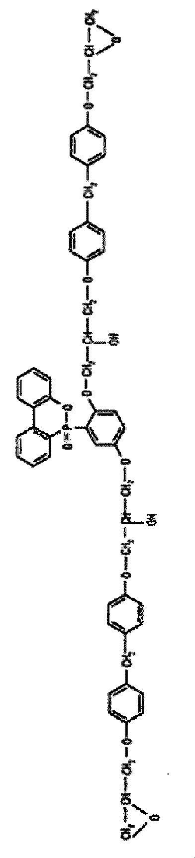
更に、C成分のリン含有エポキシ系樹脂として、以下に示す化4に示す構造式を備える化合物も好ましい。化2及び化3に示すリン含有エポキシ系樹脂と同様に、半硬化状態での樹脂品質の安定性に優れ、同時に高い難燃性の付与が可能であるため好ましい。
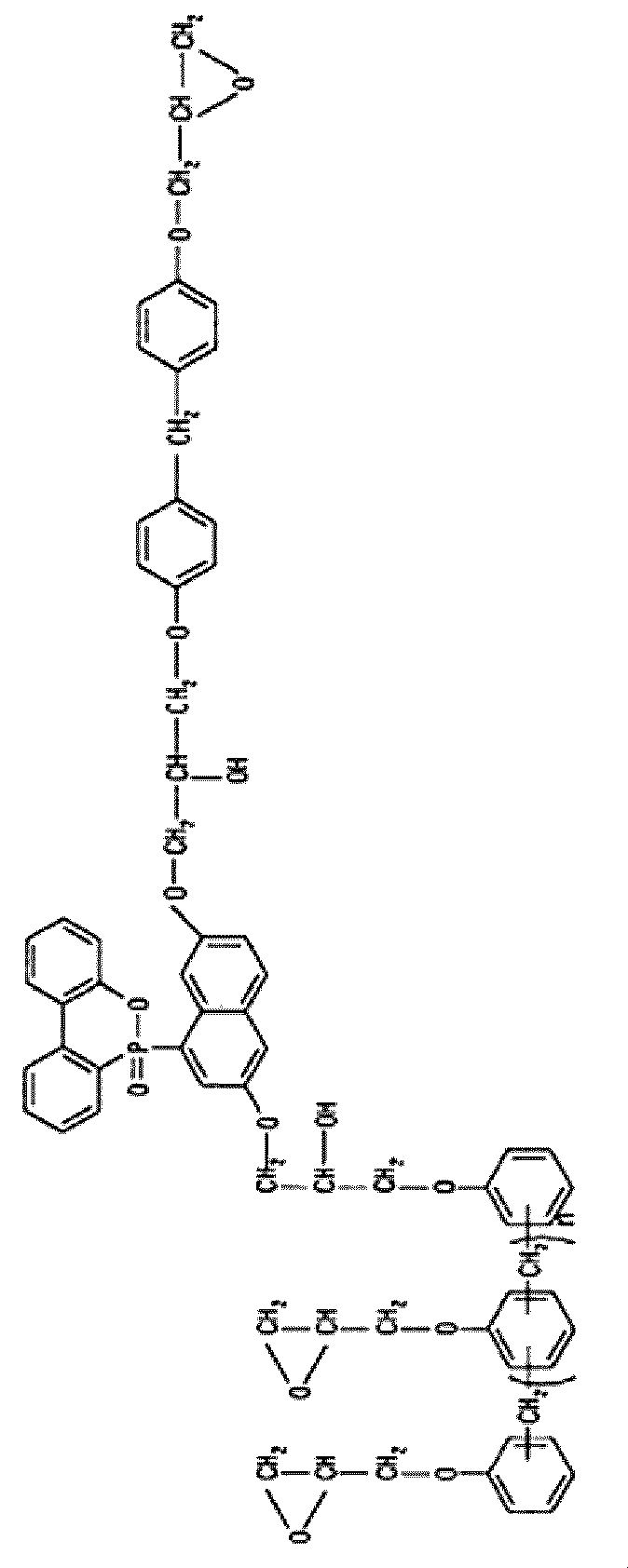
この9,10-ジヒドロ-9-オキサ-10-ホスファフェナントレン-10-オキサイドからの誘導体として得られるエポキシ樹脂は、9,10-ジヒドロ-9-オキサ-10-ホスファフェナントレン-10-オキサイドにナフトキノンやハイドロキノンを反応させて、以下の化5(HCA-NQ)又は化6(HCA-HQ)に示す化合物とした後に、そのOH基の部分にエポキシ樹脂を反応させてリン含有難燃性樹脂としたものが挙げられる。


ここで、リン含有難燃性樹脂として、リン含有エポキシ系樹脂を用いる場合の樹脂組成物は、リン含有エポキシ系樹脂の1種類を単独で用いても、2種類以上のリン含有エポキシ系樹脂を混合して用いても構わない。但し、C成分としてのリン含有難燃性樹脂の総量を考慮して、半硬化樹脂層を構成するエポキシ樹脂組成物重量を100重量%としたとき、C成分由来のリン原子を0.5重量%~3.0重量%の範囲となるように添加量を定めることが好ましい。リン含有エポキシ系樹脂は、その種類によりエポキシ骨格内に含有するリン原子量が異なる。そこで、上述のようにリン原子の含有量を、C成分の添加量に優先させて設計することが可能である。
次に、リン含有難燃性樹脂として、フォスファゼン系樹脂を用いる場合を説明する。フォスファゼン系樹脂は、リン及び窒素を構成元素とする二重結合を持つフォスファゼンを含む樹脂である。フォスファゼン系樹脂は、分子中の窒素とリンの相乗効果により、難燃性能を飛躍的に向上させることができる。また、9,10-ジヒドロ-9-オキサ-10-ホスファフェナントレン-10-オキサイド誘導体と異なり、樹脂中で安定して存在し、マイグレーションの発生を防ぐ効果が得られる。
また、リン含有難燃性樹脂として、フォスファゼン系樹脂を用いる場合の樹脂組成物は、フォスファゼン系樹脂の1種類を単独で用いても、2種類以上のフォスファゼン系樹脂を混合して用いても構わない。但し、C成分としてのリン含有難燃性樹脂の総量を考慮して、半硬化樹脂層を構成するフォスファゼン系樹脂組成物重量を100重量%としたとき、C成分由来のリン原子を0.5重量%~3.0重量%の範囲となるように添加量を定めることが好ましい。このことは、C成分として、リン含有エポキシ系樹脂とフォスファゼン系樹脂を混合して用いる場合も同様である。
そして、C成分としてのリン含有難燃性樹脂は、リン含有エポキシ系樹脂、フォスファゼン系樹脂のいずれか一種またはこれらを混合したものを用いれば良い。リン含有難燃性樹脂としてリン含有エポキシ系樹脂を単独で用いる場合は、リン含有エポキシ系樹脂は、半硬化樹脂層を構成するエポキシ樹脂組成物を100重量部としたとき、5重量部~50重量部の範囲で用いられることが好ましい。リン含有エポキシ系樹脂からなるC成分が5重量部未満の場合には、他の樹脂成分の配合割合を考慮すると、C成分由来のリン原子が不足し、難燃性を得ることが困難になる。一方、リン含有エポキシ系樹脂からなるC成分が50重量部を超えるようにしても、難燃性向上効果も飽和すると同時に、硬化後の樹脂層が脆くなるため好ましくない。
また、リン含有難燃性樹脂として、フォスファゼン系樹脂を単独で用いる場合は、フォスファゼン系樹脂は、半硬化樹脂層を構成するエポキシ樹脂組成物を100重量部としたとき、2重量部~18重量部の範囲で用いられることが好ましい。フォスファゼン系樹脂からなるC成分が2重量部未満の場合には、他の樹脂成分の配合割合を考慮すると、C成分由来のリン原子が不足し、難燃性を得ることが困難になる。一方、フォスファゼン系樹脂からなるC成分が18重量部を超えると、樹脂組成物のガラス転移点Tg、半田耐熱性、ピール強度が不十分となる傾向があるので好ましくない。
上述の硬化樹脂の「高Tg化」と「フレキシビリティ」とは、一般的に反比例する特性である。このときリン含有難燃性樹脂は、硬化後の樹脂のフレキシビリティの向上に寄与するもの、高Tg化に寄与するものが存在する。従って、1種類のリン含有難燃性エポキシ樹脂を用いるよりは、「高Tg化に寄与するリン含有難燃性エポキシ樹脂」と「フレキシビリティの向上に寄与するリン含有難燃性エポキシ樹脂」とをバランス良く配合して用いることで、フレキシブルプリント配線板用途で好適な樹脂組成とすることが可能である。
D成分は、沸点が50℃~200℃の範囲にある溶剤に可溶で、液状ゴム成分で変成されたゴム変成ポリアミドイミド樹脂である。このゴム変成ポリアミドイミド樹脂は、ポリアミドイミド樹脂とゴム性樹脂とを反応させて得られるものである。ここで言う、ゴム変成ポリアミドイミド樹脂とゴム性樹脂とを反応させて用いるのは、ポリアミドイミド樹脂そのものの柔軟性を向上させる目的で行う。すなわち、ポリアミドイミド樹脂とゴム性樹脂とを反応させ、ポリアミドイミド樹脂の酸成分(シクロヘキサンジカルボン酸等)の一部をゴム成分に置換するのである。ゴム成分としては、天然ゴム及び合成ゴムを含み、後者の合成ゴムにはスチレン-ブタジエンゴム、ブタジエンゴム、ブチルゴム、エチレン-プロピレンゴム等がある。更に、耐熱性を確保する観点からは、ニトリルゴム、クロロプレンゴム、シリコンゴム、ウレタンゴム等の耐熱性を備えた合成ゴムを選択使用することも有用である。これらのゴム性樹脂に関しては、ポリアミドイミド樹脂と反応して共重合体を製造するようになるため、両末端に種々の官能基を備えるものであることが望ましい。特に、カルボキシル基を有するCTBN(カルボキシ基末端ブタジエンニトリル)を用いることが有用である。なお、上記ゴム成分は、1種のみを共重合させても、2種以上を共重合させても構わない。更に、ゴム成分を用いる場合には、そのゴム成分の数平均分子量が1000以上のものを用いることが、当該フレキシビリティの安定化の観点から好ましい。
ゴム変成ポリアミドイミド樹脂を重合させる際に、ポリアミドイミド樹脂とゴム性樹脂との溶解に使用する溶剤には、ジメチルホルムアミド、ジメチルアセトアミド、N-メチル-2-ピロリドン、ジメチルスルホキシド、ニトロメタン、ニトロエタン、テトラヒドロフラン、シクロヘキサノン、メチルエチルケトン、アセトニトリル、γ-ブチロラクトン等を、1種又は2種以上を混合して用いることが好ましい。そして、重合反応を起こさせるには、80℃~200℃の範囲の重合温度を採用することが好ましい。これらの重合に沸点が200℃を超える溶剤を用いた場合には、その後、用途に応じて沸点が50℃~200℃の範囲にある溶剤に溶媒置換することが好ましい。
ここで、前記沸点が50℃~200℃の範囲にある溶剤とは、メチルエチルケトン、ジメチルアセトアミド、ジメチルホルムアミド等の群から選ばれる1種の単独溶剤又は2種以上の混合溶剤が挙げられる。沸点が50℃未満の場合には、加熱による溶剤の気散が著しくなり、樹脂ワニスの状態から半硬化樹脂とする場合に、良好な半硬化状態が得られにくくなる。一方、沸点が200℃を超える場合には、樹脂ワニスの状態から半硬化樹脂とする場合に、バブリングが起こりやすくなるため、良好な半硬化樹脂膜を得にくくなる。
エポキシ樹脂組成物で用いるゴム変成ポリアミドイミド樹脂の中で、ゴム変成ポリアミドイミド樹脂の重量を100重量%としたとき、ゴム成分の共重合量は0.8重量%以上であることが好ましい。当該共重合量が0.8重量%未満の場合には、ゴム変成ポリアミドイミド樹脂としても、本件発明に言うエポキシ樹脂組成物を用いて形成した樹脂層を硬化させたときのフレキシビリティが欠如し、銅箔との密着性も低下するため好ましくない。なお、より好ましくは、当該ゴム成分の共重合量は3重量%以上、更に好ましくは5重量%以上がより好ましい。経験的に40重量%を超えてゴム成分の添加量を向上させても、特段の問題はない。しかし、当該硬化後の樹脂層のフレキシビリティの向上効果は飽和するために資源の無駄となり好ましくない。
以上に述べてきたゴム変成ポリアミドイミド樹脂には、溶剤に可溶であるという性質が求められる。溶剤に可溶でなければ、樹脂ワニスとしての調製が困難だからである。このゴム変成ポリアミドイミド樹脂は、樹脂組成物の重量を100重量部としたとき、10重量部~40重量部の配合割合で用いることが好ましい。ゴム変成ポリアミドイミド樹脂が10重量部未満の場合には、硬化後の樹脂層のフレキシビリティは向上させ得ず脆くなり、樹脂層へのマイクロクラックを生じやすくなる。一方、40重量部を越えてゴム変成ポリアミドイミド樹脂を添加しても特に支障はないが、それ以上に硬化後の樹脂層のフレキシビリティは向上せず、硬化後の樹脂の高Tg化が図れない。従って、経済性を考慮すれば、40重量部が上限値であると言える。
E成分の樹脂硬化剤に関して述べる。ここで言う樹脂硬化剤は、ビフェニル型フェノール樹脂、フェノールアラルキル型フェノール樹脂の1種又は2種以上を用いることが好ましい。この樹脂硬化剤の添加量は、硬化させる樹脂に対する反応当量から自ずと導き出されるものであり、特段の量的な限定を要するものではない。しかしながら、本件発明に用いるエポキシ樹脂組成物の場合には、当該エポキシ樹脂組成物を100重量部としたとき、E成分を20重量部~35重量部の範囲で用いることが好ましい。このE成分が20重量部未満の場合には、上記樹脂組成を考慮すると、十分な硬化状態を得ることが出来なくなり、硬化後の樹脂としてフレキシビリティを得ることが出来なくなる。一方、E成分が35重量部を超える場合には、硬化した後の樹脂層の耐吸湿特性が劣化する傾向にあり、好ましくない。
以上に示した樹脂組成物に溶剤を加えて樹脂ワニスとして用い、プリント配線板の接着層として熱硬化性樹脂層を形成する。当該樹脂ワニスは、上述の樹脂組成物に溶剤を加えて、樹脂固形分量が30wt%~70wt%の範囲に調製し、MIL規格におけるMIL-P-13949Gに準拠して測定したときのレジンフローが5%~35%の範囲にある半硬化樹脂膜の形成が可能なことを特徴とする。ここで言う溶剤には、沸点が50℃~200℃の範囲であり、メチルエチルケトン、ジメチルアセトアミド、ジメチルホルムアミド等の群から選ばれる1種の単独溶剤又は2種以上の混合溶剤を用いることが好ましい。上述のように良好な半硬化樹脂膜を得るためである。そして、ここに示した樹脂固形分量の範囲が、銅箔の表面に塗布したときに、最も膜厚を精度の良いものに制御できる範囲である。樹脂固形分が30wt%未満の場合には、粘度が低すぎて、銅箔表面への塗布直後に流れて膜厚均一性を確保しにくい。これに対して、樹脂固形分が70wt%を越えると、粘度が高くなり、銅箔表面への薄膜形成が困難となる。なお、レジンフローが、5%未満の場合には、内層コア材の表面にある内層回路の凹凸部等にエアーの噛み込み等を起こすため好ましくない。一方、当該レジンフローが、35%を超える場合には、レジンフローが大きくなりすぎて、樹脂層を有するキャリア付銅箔の樹脂層を用いて形成する絶縁層の厚さが不均一になる。
キャリア付銅箔に前記硬化樹脂層および、半硬化樹脂層を設けた場合、立体成型プリント配線板製造用途に適した、樹脂層を有するキャリア付銅箔を提供することができる。
キャリア付銅箔に前記硬化樹脂層および、半硬化樹脂層を設けた場合、立体成型プリント配線板製造用途に適した、樹脂層を有するキャリア付銅箔を提供することができる。
また、前記樹脂層は前記半硬化絶縁層の片面に引き剥がし可能な保護フィルムを備えることが好ましい。前記保護フィルムには公知の絶縁フィルムや樹脂フィルムを用いることができる。例えば、ポリエチレンテレフタレートフィルム、ポリエチレンナフタレートフィルム、金属箔等を前記保護フィルムに用いることができる。
なお、前記樹脂層は硬化剤および/または硬化促進剤を含んでもよい。
前記樹脂層はMIL規格におけるMIL-P-13949Gに準拠して測定したときのレジンフローが5%以内である樹脂組成物で形成された樹脂層であってもよい。
前記樹脂層は5重量部~50重量部のエポキシ樹脂(硬化剤を含む)、50重量部~95重量部の溶剤に可溶なポリエーテルサルホン、及び、必要に応じて適宜量添加する硬化促進剤からなる樹脂組成物を用いて構成したものであってもよい。
なお、前記樹脂層は硬化剤および/または硬化促進剤を含んでもよい。
前記樹脂層はMIL規格におけるMIL-P-13949Gに準拠して測定したときのレジンフローが5%以内である樹脂組成物で形成された樹脂層であってもよい。
前記樹脂層は5重量部~50重量部のエポキシ樹脂(硬化剤を含む)、50重量部~95重量部の溶剤に可溶なポリエーテルサルホン、及び、必要に応じて適宜量添加する硬化促進剤からなる樹脂組成物を用いて構成したものであってもよい。
また、前記樹脂層は以下に示す成分A~成分Dを、下記含有量(但し、エポキシ樹脂
硬化剤を除き、樹脂組成物を100重量部としたときの重量部として記載)の範囲で含む
樹脂組成物で形成したものであってもよい。
成分A: 25℃における引張強度200MPa以上のポリアミドイミド樹脂 10重量
部~20重量部
成分B: 25℃における引張強度100MPa以下のポリアミドイミド樹脂 20重量
部~40重量部
成分C: エポキシ樹脂
成分D: エポキシ樹脂硬化剤
前記樹脂層は半硬化樹脂層であってもよい。
硬化剤を除き、樹脂組成物を100重量部としたときの重量部として記載)の範囲で含む
樹脂組成物で形成したものであってもよい。
成分A: 25℃における引張強度200MPa以上のポリアミドイミド樹脂 10重量
部~20重量部
成分B: 25℃における引張強度100MPa以下のポリアミドイミド樹脂 20重量
部~40重量部
成分C: エポキシ樹脂
成分D: エポキシ樹脂硬化剤
前記樹脂層は半硬化樹脂層であってもよい。
前記成分Aは、25℃における引張強度200MPa以上のポリアミドイミド樹脂である。ここで言う「引張強度200MPa以上のポリアミドイミド樹脂」とは、例えば、トリメリット酸無水物、ベンゾフェノンテトラカルボン酸無水物及びビトリレンジイソシアネートをN-メチル-2-ピロリドン又は/及びN,N-ジメチルアセトアミド等の溶剤中で加熱することで得られる樹脂等である。ここで、上限値を記載していないがポリイミドアミド樹脂の引張強度を考慮すると、このポリアミドイミド樹脂の引張強度の上限は、500MPa程度である。なお、本件発明における成分A及び成分Bに係るポリアミドイミド樹脂の引張強度は、ポリアミドイミド樹脂溶液から、JIS K7113に定めるフィルム状の2号試験片(全長115mm、チャック間距離80±5mm、平行部長さ33±2mm、平行部幅6±0.4mm、フィルム厚1~3mm)を用いて、引張試験機で測定した値である。
前記成分Bは、25℃における引張強度100MPa以下のポリアミドイミド樹脂である。ここで言う「引張強度100MPa以下のポリアミドイミド樹脂」とは、例えば、トリメリット酸無水物、ジフェニルメタンジイソシアネート及びカルボキシル基末端アクリロニトリル-ブタジエンゴムをN-メチル-2-ピロリドン又は/及びN,N-ジメチルアセトアミド等の溶剤中で加熱することで得られるものである。
前記成分C(エポキシ樹脂)の含有量は、樹脂組成物を100重量部としたとき、40重量部~70重量部であってもよい。なお、エポキシ樹脂としては前述のエポキシ樹脂を用いることができる。前記成分D(エポキシ樹脂硬化剤)の含有量は、樹脂組成物に対して、エポキシ樹脂の硬化可能な程度のイミダゾール化合物を含有させるものであることが好ましい。前記半硬化樹脂層は、前記樹脂組成物で形成した揮発分が1wt%未満の半硬化状態の樹脂層であることが好ましい。上記含有量を満たした場合、樹脂層を有するキャリア付銅箔をロール状で保管又は輸送しても、樹脂層を有するキャリア付銅箔の樹脂層からキャリア付銅箔への有機溶剤の転写が無く、しかも、耐熱性、キャリア付銅箔との接着性の各特性に優れる樹脂層を備えるキャリア付銅箔を得ることができる。
前記成分C(エポキシ樹脂)の含有量は、樹脂組成物を100重量部としたとき、40重量部~70重量部であってもよい。なお、エポキシ樹脂としては前述のエポキシ樹脂を用いることができる。前記成分D(エポキシ樹脂硬化剤)の含有量は、樹脂組成物に対して、エポキシ樹脂の硬化可能な程度のイミダゾール化合物を含有させるものであることが好ましい。前記半硬化樹脂層は、前記樹脂組成物で形成した揮発分が1wt%未満の半硬化状態の樹脂層であることが好ましい。上記含有量を満たした場合、樹脂層を有するキャリア付銅箔をロール状で保管又は輸送しても、樹脂層を有するキャリア付銅箔の樹脂層からキャリア付銅箔への有機溶剤の転写が無く、しかも、耐熱性、キャリア付銅箔との接着性の各特性に優れる樹脂層を備えるキャリア付銅箔を得ることができる。
ここで、イミダゾール化合物は、公知のものを用いることができ、例えば、2-ウンデシルイミダゾール、2-ヘプタデシルイミダゾール、2-エチル-4-メチルイミダゾール、2-フェニル-4-メチルイミダゾール、1-シアノエチル-2-ウンデシルイミダゾール、1-シアノエチル-2-エチル-4-メチルイミダゾール、1-シアノエチル-2-フェニルイミダゾール、2-フェニル-4,5-ジヒドロキシメチルイミダゾール、2-フェニル-4-メチル-5-ヒドロキシメチルイミダゾールなどが挙げられ、これらを単独若しくは混合して用いることができる。
なお、添加すべき硬化剤の量は、エポキシ樹脂の量、工程で要求する硬化速度等に応じて必然的に定まるものである。敢えて硬化剤としてのイミダゾール化合物の添加量を記載すると、樹脂組成物100重量部としたとき(但し、この場合は、成分A~成分D全ての樹脂組成物を100重量部としたときの重量部として記載)、当該樹脂組成物中に0.01重量部~2重量部の範囲で配合して用いる。そして、イミダゾール化合物の配合量は、0.02重量部~1.5重量部がより好ましく、更に好ましくは、0.03重量部~1.0重量部である。このイミダゾール化合物の配合量が0.01重量部未満の場合には、上記エポキシ樹脂の含有量を考慮すると硬化が不十分となる場合があり、樹脂層を有するキャリア付銅箔の樹脂層同士を張り合わせる際の接着強度が低下する。一方、イミダゾール化合物の配合量が2重量部を超える場合には、エポキシ樹脂の硬化反応が速くなり、硬化後の樹脂層が脆くなり、硬化樹脂フィルムの強度、樹脂付銅箔の樹脂層同士を張り合わせる際の接着性が低下する場合がある。
なお、成分Cのエポキシ樹脂、成分Dのエポキシ樹脂硬化剤には公知の成分Cのエポキシ樹脂、成分Dのエポキシ樹脂硬化剤または本願明細書に記載の成分Cのエポキシ樹脂、成分Dのエポキシ樹脂硬化剤を用いることができる。
なお、成分Cのエポキシ樹脂、成分Dのエポキシ樹脂硬化剤には公知の成分Cのエポキシ樹脂、成分Dのエポキシ樹脂硬化剤または本願明細書に記載の成分Cのエポキシ樹脂、成分Dのエポキシ樹脂硬化剤を用いることができる。
前記樹脂層は半硬化状態における耐吸湿特性を備える樹脂組成物であって、当該樹脂組成物は、以下のA成分~E成分を含み、樹脂組成物重量を100重量%としたときリン原子を0.5重量%~3.0重量%の範囲で含有した樹脂組成物を用いて形成されてもよい。
A成分: エポキシ当量が200以下で、25℃で液状のビスフェノールA型エポキシ樹脂、ビスフェノールF型エポキシ樹脂、ビスフェノールAD型エポキシ樹脂の群から選ばれる1種又は2種以上。
B成分: 架橋可能な官能基を有する線状ポリマー。
C成分: 架橋剤。
D成分: イミダゾール系エポキシ樹脂硬化剤。
E成分: リン含有エポキシ樹脂。
前記B成分である官能基を有する線状ポリマーは、沸点が50℃~200℃の温度の有機溶剤に可溶なポリマー成分であることが好ましい。具体的にはポリビニルアセタール樹脂、フェノキシ樹脂、ポリエーテルスルホン樹脂、ポリアミドイミド樹脂等である。前記架橋可能な官能基を有する線状ポリマーは、樹脂組成物を100重量部としたとき、3重量部~30重量部の配合割合で用いられることが好ましい。当該エポキシ樹脂が3重量部未満の場合には、樹脂流れが大きくなる場合がある。この結果、製造した銅張積層板の端部から樹脂粉の発生が多く見られる場合があり、半硬化状態での樹脂層の耐吸湿性も改善出来ない場合がある。一方、30重量部を超えても、樹脂流れが小さい場合があり、製造した銅張積層板の絶縁層内にボイド等の欠陥を生じやすくなる場合がある。
A成分: エポキシ当量が200以下で、25℃で液状のビスフェノールA型エポキシ樹脂、ビスフェノールF型エポキシ樹脂、ビスフェノールAD型エポキシ樹脂の群から選ばれる1種又は2種以上。
B成分: 架橋可能な官能基を有する線状ポリマー。
C成分: 架橋剤。
D成分: イミダゾール系エポキシ樹脂硬化剤。
E成分: リン含有エポキシ樹脂。
前記B成分である官能基を有する線状ポリマーは、沸点が50℃~200℃の温度の有機溶剤に可溶なポリマー成分であることが好ましい。具体的にはポリビニルアセタール樹脂、フェノキシ樹脂、ポリエーテルスルホン樹脂、ポリアミドイミド樹脂等である。前記架橋可能な官能基を有する線状ポリマーは、樹脂組成物を100重量部としたとき、3重量部~30重量部の配合割合で用いられることが好ましい。当該エポキシ樹脂が3重量部未満の場合には、樹脂流れが大きくなる場合がある。この結果、製造した銅張積層板の端部から樹脂粉の発生が多く見られる場合があり、半硬化状態での樹脂層の耐吸湿性も改善出来ない場合がある。一方、30重量部を超えても、樹脂流れが小さい場合があり、製造した銅張積層板の絶縁層内にボイド等の欠陥を生じやすくなる場合がある。
また、ここで言う沸点が50℃~200℃の温度の有機溶剤を具体的に例示すると、メタノール、エタノール、メチルエチルケトン、トルエン、プロピレングリコールモノメチルエーテル、ジメチルホルムアミド、ジメチルアセトアミド、シクロヘキサノン、エチルセロソルブ等の群から選ばれる1種の単独溶剤又は2種以上の混合溶剤である。沸点が50℃未満の場合には、加熱による溶剤の気散が著しく、樹脂ワニスの状態から半硬化樹脂とする場合に、良好な半硬化状態が得られにくくなる場合がある。一方、沸点が200℃を超える場合には、半硬化状態で溶剤が残りやすい場合がある。そして、通常要求される揮発速度を満足せず、工業生産性を満足しない可能性がある。
C成分は、B成分とエポキシ樹脂との架橋反応を起こさせるための架橋剤である。この架橋剤には、ウレタン系樹脂を使用することが好ましい。この架橋剤は、B成分の混合量に応じて添加されるものであり、本来厳密にその配合割合を明記する必要性はないものと考える。しかしながら、樹脂組成物を100重量部としたとき、10重量部以下の配合割合で用いる事が好ましい。10重量部を超えて、ウレタン系樹脂であるC成分が存在すると、半硬化状態での樹脂層の耐吸湿性が劣化し、硬化後の樹脂層が脆くなるからである。
C成分は、B成分とエポキシ樹脂との架橋反応を起こさせるための架橋剤である。この架橋剤には、ウレタン系樹脂を使用することが好ましい。この架橋剤は、B成分の混合量に応じて添加されるものであり、本来厳密にその配合割合を明記する必要性はないものと考える。しかしながら、樹脂組成物を100重量部としたとき、10重量部以下の配合割合で用いる事が好ましい。10重量部を超えて、ウレタン系樹脂であるC成分が存在すると、半硬化状態での樹脂層の耐吸湿性が劣化し、硬化後の樹脂層が脆くなるからである。
D成分は、イミダゾール系エポキシ樹脂硬化剤である。本件発明に係る樹脂組成物で、半硬化状態の樹脂層の耐吸湿性を向上させるという観点からイミダゾール系エポキシ樹脂硬化剤を選択的に用いる事が好ましい。中でも、以下の化7に示す構造式を備えるイミダゾール系エポキシ樹脂硬化剤を用いる事が好ましい。この化7に示す構造式のイミダゾール系エポキシ樹脂硬化剤を用いることで、半硬化状態の樹脂層の耐吸湿性を顕著に向上でき、長期保存安定性に優れる。なお、エポキシ樹脂に対するエポキシ樹脂硬化剤の添加量は、反応当量から計算するのではなく、実験上得られる最適量を採用することが好ましい。イミダゾール系エポキシ樹脂硬化剤は、エポキシ樹脂の硬化に際して触媒的な働きを行うものであり、硬化反応の初期段階において、エポキシ樹脂の自己重合反応を引き起こす反応開始剤として寄与するからである。
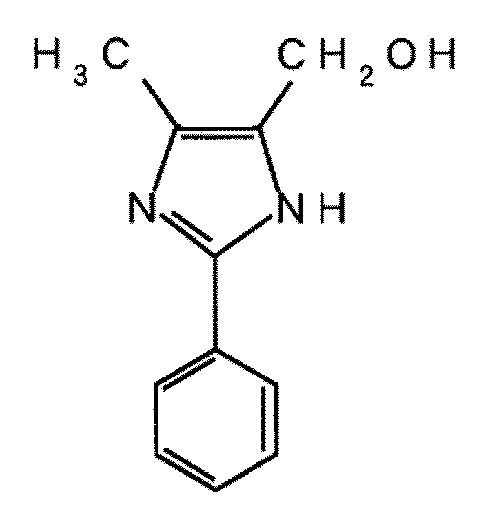
前記E成分であるリン含有エポキシ樹脂は、分子内に2以上のエポキシ基を備える9,10-ジヒドロ-9-オキサ-10-ホスファフェナントレン-10-オキサイドからの誘導体として得られるエポキシ樹脂であることが好ましい。
10-ジヒドロ-9-オキサ-10-ホスファフェナントレン-10-オキサイドの構造式は下記の通りである。
10-ジヒドロ-9-オキサ-10-ホスファフェナントレン-10-オキサイドの構造式は下記の通りである。

この9,10-ジヒドロ-9-オキサ-10-ホスファフェナントレン-10-オキサイドからの誘導体として得られるエポキシ樹脂は、9,10-ジヒドロ-9-オキサ-10-ホスファフェナントレン-10-オキサイドにナフトキノンやハイドロキノンを反応させて、以下の化9(HCA-NQ)又は化10(HCA-HQ)に示す化合物とした後に、そのOH基の部分にエポキシ樹脂を反応させてリン含有エポキシ樹脂としたものである。
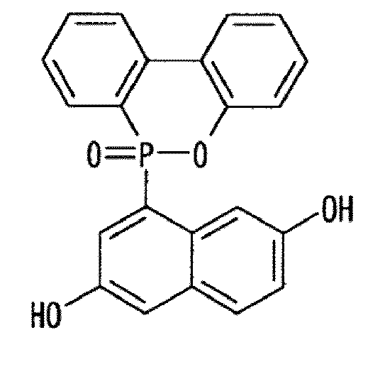
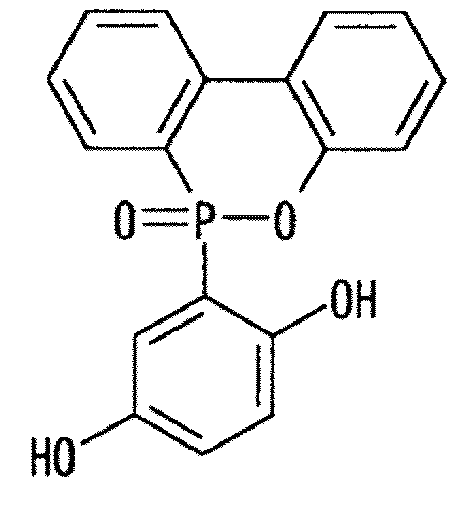
上述の化合物を原料として得られた前記E成分であるリン含有エポキシ樹脂は、以下に示す化11~化13のいずれかに示す構造式を備える化合物の1種又は2種を混合して用いることが好ましい。半硬化状態での樹脂品質の安定性に優れ、同時に難燃性効果が高いためである。


前記樹脂組成物は樹脂組成物重量を100重量部としたとき、A成分が3重量部~20重量部、B成分が3重量部~30重量部、樹脂組成物重量を100重量%としたときリン原子を0.5重量%~3.0重量%の範囲となるようにE成分の重量部を定める樹脂組成物であることが好ましい。
前記樹脂層は、以下のA成分~F成分の各成分を含む樹脂組成物を用いて形成してもよい。
A成分: エポキシ当量が200以下で、25℃で液状のビスフェノールA型エポキシ樹脂、ビスフェノールF型エポキシ樹脂、ビスフェノールAD型エポキシ樹脂の群から選ばれる1種又は2種以上。
B成分: 架橋可能な官能基を有する線状ポリマー。
C成分: 架橋剤(但し、A成分がB成分の架橋剤として機能する場合には省略可。)。D成分: 4,4’-ジアミノジフェニルスルホン又は2,2-ビス(4-(4-アミノフェノキシ)フェニル)プロパン。
E成分: 難燃性エポキシ樹脂。
F成分: 多官能エポキシ樹脂。
G成分: 硬化促進剤。
前記B成分である架橋可能な官能基を有する線状ポリマーは、ポリビニルアセタール樹脂又はポリアミドイミド樹脂であることが好ましい。
前記C成分である架橋剤は、ウレタン系樹脂であることが好ましい。
前記E成分である難燃性エポキシ樹脂は、分子内に2以上のエポキシ基を備えるテトラブロモビスフェノールAからの誘導体として得られる化14に示す構造式を備える臭素化エポキシ樹脂、以下に示す化15に示す構造式を備える臭素化エポキシ樹脂の1種又は2種を混合して用いることが好ましい。
A成分: エポキシ当量が200以下で、25℃で液状のビスフェノールA型エポキシ樹脂、ビスフェノールF型エポキシ樹脂、ビスフェノールAD型エポキシ樹脂の群から選ばれる1種又は2種以上。
B成分: 架橋可能な官能基を有する線状ポリマー。
C成分: 架橋剤(但し、A成分がB成分の架橋剤として機能する場合には省略可。)。D成分: 4,4’-ジアミノジフェニルスルホン又は2,2-ビス(4-(4-アミノフェノキシ)フェニル)プロパン。
E成分: 難燃性エポキシ樹脂。
F成分: 多官能エポキシ樹脂。
G成分: 硬化促進剤。
前記B成分である架橋可能な官能基を有する線状ポリマーは、ポリビニルアセタール樹脂又はポリアミドイミド樹脂であることが好ましい。
前記C成分である架橋剤は、ウレタン系樹脂であることが好ましい。
前記E成分である難燃性エポキシ樹脂は、分子内に2以上のエポキシ基を備えるテトラブロモビスフェノールAからの誘導体として得られる化14に示す構造式を備える臭素化エポキシ樹脂、以下に示す化15に示す構造式を備える臭素化エポキシ樹脂の1種又は2種を混合して用いることが好ましい。
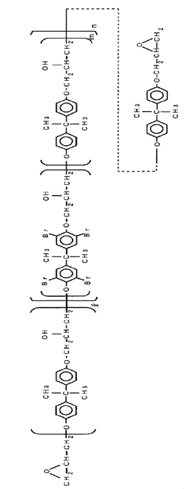
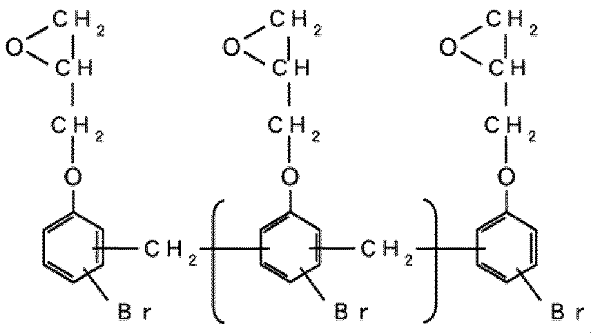
前記E成分である難燃性エポキシ樹脂は、分子内に2以上のエポキシ基を備える9,10-ジヒドロ-9-オキサ-10-ホスファフェナントレン-10-オキサイド誘導体であるリン含有エポキシ樹脂を用いることが好ましい。
前記E成分である難燃性エポキシ樹脂は、以下に示す化16~化18のいずれかに示す構造式を備えるリン含有エポキシ樹脂の1種又は2種を混合して用いることが好ましい。
前記E成分である難燃性エポキシ樹脂は、以下に示す化16~化18のいずれかに示す構造式を備えるリン含有エポキシ樹脂の1種又は2種を混合して用いることが好ましい。
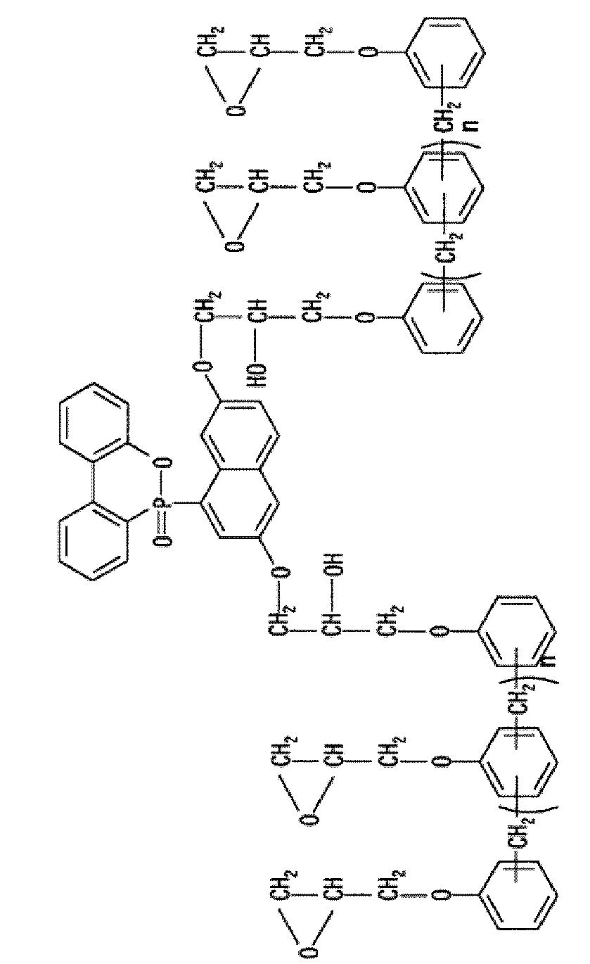

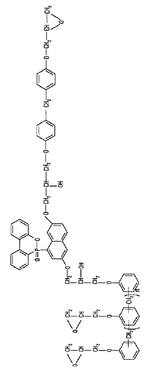
前記F成分の多官能エポキシ樹脂としてオルトクレゾールノボラック型エポキシ樹脂を用いることが好ましい。
前記樹脂層を形成するための樹脂組成物の重量を100重量部としたとき、A成分が3重量部~20重量部、B成分が3重量部~30重量部、C成分が3重量部~10重量部(A成分がB成分の架橋剤として機能する場合には0重量部~10重量部)、D成分が5重量部~20重量部、F成分が3重量部~20重量部であり、樹脂組成物重量を100重量%としたとき、E成分由来の臭素原子を12重量%~18重量%の範囲含有するようにE成分の重量部を定めることが好ましい。
前記樹脂層を形成するための樹脂組成物の重量を100重量部としたとき、A成分が3重量部~20重量部、B成分が3重量部~30重量部、C成分が3重量部~10重量部(A成分がB成分の架橋剤として機能する場合には0重量部~10重量部)、D成分が5重量部~20重量部、F成分が3重量部~20重量部であり、樹脂組成物重量を100重量%としたとき、E成分由来のリン原子を0.5重量%~3.0重量%の範囲含有するようにE成分の重量部を定めるものであることが好ましい。
前記樹脂層を形成するための樹脂組成物はG成分として硬化促進剤を含むことが好ましい。
前記樹脂層は 以下の工程a、工程bの手順で樹脂層の形成に用いる樹脂ワニスを調製し、当該樹脂ワニスをキャリア付銅箔の表面に塗布し、乾燥させることで5μm~100μmの平均厚さの半硬化樹脂膜を形成してされることが好ましい。
工程a: 前記A成分、B成分、C成分(A成分がB成分の架橋剤として機能する場合には省略可)、D成分、E成分、F成分、G成分の内、A成分~F成分を必須成分とした樹脂組成物の重量を100重量%としたとき、E成分由来の臭素原子を12重量%~18重量%の範囲又はリン原子を0.5重量%~3.0重量%の範囲で含有するように各成分を混合して樹脂組成物とする。
工程b: 前記樹脂組成物を、有機溶剤を用いて溶解し、樹脂固形分量が25重量%~50重量%の樹脂ワニスとする。
前記樹脂層を形成するための樹脂組成物の重量を100重量部としたとき、A成分が3重量部~20重量部、B成分が3重量部~30重量部、C成分が3重量部~10重量部(A成分がB成分の架橋剤として機能する場合には0重量部~10重量部)、D成分が5重量部~20重量部、F成分が3重量部~20重量部であり、樹脂組成物重量を100重量%としたとき、E成分由来の臭素原子を12重量%~18重量%の範囲含有するようにE成分の重量部を定めることが好ましい。
前記樹脂層を形成するための樹脂組成物の重量を100重量部としたとき、A成分が3重量部~20重量部、B成分が3重量部~30重量部、C成分が3重量部~10重量部(A成分がB成分の架橋剤として機能する場合には0重量部~10重量部)、D成分が5重量部~20重量部、F成分が3重量部~20重量部であり、樹脂組成物重量を100重量%としたとき、E成分由来のリン原子を0.5重量%~3.0重量%の範囲含有するようにE成分の重量部を定めるものであることが好ましい。
前記樹脂層を形成するための樹脂組成物はG成分として硬化促進剤を含むことが好ましい。
前記樹脂層は 以下の工程a、工程bの手順で樹脂層の形成に用いる樹脂ワニスを調製し、当該樹脂ワニスをキャリア付銅箔の表面に塗布し、乾燥させることで5μm~100μmの平均厚さの半硬化樹脂膜を形成してされることが好ましい。
工程a: 前記A成分、B成分、C成分(A成分がB成分の架橋剤として機能する場合には省略可)、D成分、E成分、F成分、G成分の内、A成分~F成分を必須成分とした樹脂組成物の重量を100重量%としたとき、E成分由来の臭素原子を12重量%~18重量%の範囲又はリン原子を0.5重量%~3.0重量%の範囲で含有するように各成分を混合して樹脂組成物とする。
工程b: 前記樹脂組成物を、有機溶剤を用いて溶解し、樹脂固形分量が25重量%~50重量%の樹脂ワニスとする。
前記樹脂層は以下のA成分~E成分の各成分を含む樹脂組成物を用いて形成されることが好ましい。
A成分: エポキシ当量が200以下で、室温で液状のビスフェノールA型エポキシ樹脂、ビスフェノールF型エポキシ樹脂、ビスフェノールAD型エポキシ樹脂の群から選ばれる1種又は2種以上からなるエポキシ樹脂。
B成分: 高耐熱性エポキシ樹脂。
C成分: リンを含有した難燃性エポキシ樹脂。
D成分: 沸点が50℃~200℃の範囲にある溶剤に可溶な性質を備える液状ゴム成分で変成したゴム変成ポリアミドイミド樹脂。
E成分: ビフェニル型フェノール樹脂、フェノールアラルキル型フェノール樹脂の1種又は2種以上からなる樹脂硬化剤。
前記樹脂層は前記A成分~E成分の各成分に加えて、更にF成分としてエポキシ樹脂との反応性を有さないリン含有難燃剤を含む樹脂組成物を用いて形成されることが好ましい。
A成分: エポキシ当量が200以下で、室温で液状のビスフェノールA型エポキシ樹脂、ビスフェノールF型エポキシ樹脂、ビスフェノールAD型エポキシ樹脂の群から選ばれる1種又は2種以上からなるエポキシ樹脂。
B成分: 高耐熱性エポキシ樹脂。
C成分: リンを含有した難燃性エポキシ樹脂。
D成分: 沸点が50℃~200℃の範囲にある溶剤に可溶な性質を備える液状ゴム成分で変成したゴム変成ポリアミドイミド樹脂。
E成分: ビフェニル型フェノール樹脂、フェノールアラルキル型フェノール樹脂の1種又は2種以上からなる樹脂硬化剤。
前記樹脂層は前記A成分~E成分の各成分に加えて、更にF成分としてエポキシ樹脂との反応性を有さないリン含有難燃剤を含む樹脂組成物を用いて形成されることが好ましい。
A成分は、エポキシ当量が200以下で、室温で液状のビスフェノールA型エポキシ樹脂、ビスフェノールF型エポキシ樹脂、ビスフェノールAD型エポキシ樹脂の群から選ばれる1種又は2種以上からなるエポキシ樹脂である。ここで、ビスフェノール系エポキシ樹脂を選択使用しているのは、後述するD成分(ゴム変成ポリアミドイミド樹脂)との相性が良く、半硬化状態での樹脂膜に適度なフレキシビリティの付与が容易だからである。そして、エポキシ当量が200を超えると、樹脂が室温で半固形となり、半硬化状態でのフレキシビリティーが減少するので好ましくない。更に、上述のビスフェノール系エポキシ樹脂であれば、1種を単独で用いても、2種以上を混合で用いても構わない。しかも、2種以上を混合して用いる場合には、その混合比に関しても特段の限定はない。
このエポキシ樹脂は、樹脂組成物を100重量部としたとき、3重量部~20重量部の配合割合で用いることが好ましい。当該エポキシ樹脂が3重量部未満の場合には、熱硬化性を十分に発揮せず内層フレキシブルプリント配線板とのバインダーとしての機能も、樹脂付銅箔としての銅箔との密着性も十分に果たし難くなる。一方、20重量部を超えると、他の樹脂成分とのバランスから樹脂ワニスとしたときの粘度が高くなり、樹脂付銅箔を製造するとき、銅箔表面へ均一な厚さでの樹脂膜の形成が困難となる。しかも、後述するD成分(ゴム変成ポリアミドイミド樹脂)との添加量を考慮すると、硬化後の樹脂層として十分な靭性が得られなくなる。
B成分は、所謂ガラス転移点の高い「高耐熱性エポキシ樹脂」である。ここで言う「高耐熱性エポキシ樹脂」は、ノボラック型エポキシ樹脂、クレゾールノボラック型エポキシ樹脂、フェノールノボラック型エポキシ樹脂、ナフタレン型エポキシ樹脂等の多官能エポキシ樹脂であることが好ましい。そして、このB成分は、樹脂組成物を100重量部としたとき、3重量部~30重量部の範囲で用いることが好ましい。B成分が3重量部未満の場合には、樹脂組成物の高Tg化が全く図れない。一方、B成分が30重量部を超える場合には、硬化後の樹脂が脆くなり、フレキシビリティが完全に損なわれるためフレキシブルプリント配線板用途として好ましくない。より好ましくは、B成分は、10重量部~20重量部の範囲で用いることで、樹脂組成物の高Tg化と硬化後の樹脂の良好なフレキシビリティとを安定して両立できる。
C成分としては、所謂ハロゲンフリー系の難燃性エポキシ樹脂であり、リン含有難燃性エポキシ樹脂を用いる。リン含有難燃性エポキシ樹脂とは、エポキシ骨格の中にリンを含んだエポキシ樹脂の総称である。そして、本件出願に係る樹脂組成物のリン原子含有量を、樹脂組成物重量を100重量%としたとき、C成分由来のリン原子を0.5重量%~3.0重量%の範囲とできるリン含有難燃性エポキシ樹脂であれば、いずれの使用も可能である。しかしながら、分子内に2以上のエポキシ基を備える9,10-ジヒドロ-9-オキサ-10-ホスファフェナントレン-10-オキサイド誘導体であるリン含有難燃性エポキシ樹脂を用いることが、半硬化状態での樹脂品質の安定性に優れ、同時に難燃性効果が高いため好ましい。参考のために、9,10-ジヒドロ-9-オキサ-10-ホスファフェナントレン-10-オキサイドの構造式を化19に示す。

そして、9,10-ジヒドロ-9-オキサ-10-ホスファフェナントレン-10-オキサイド誘導体であるリン含有難燃性エポキシ樹脂を具体的に例示すると、化20に示す構造式を備える化合物の使用が好ましい。半硬化状態での樹脂品質の安定性に優れ、同時に難燃性効果が高いため好ましい。
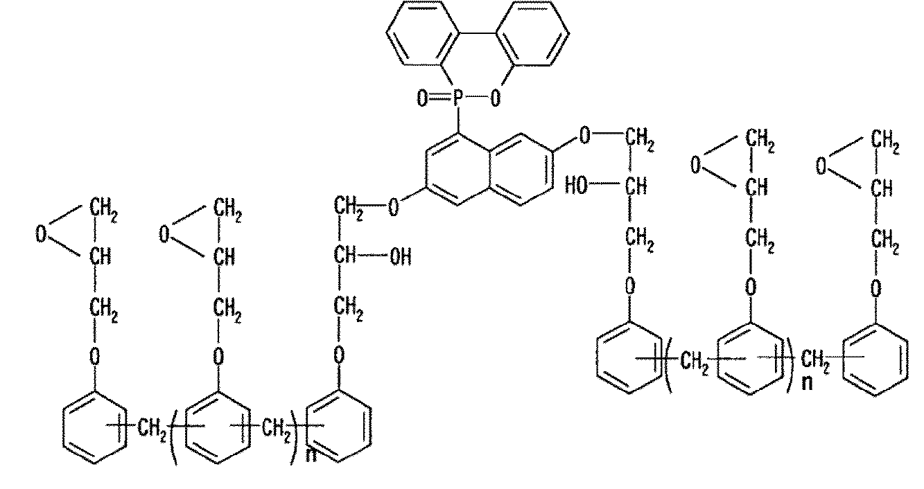
また、C成分のリン含有難燃性エポキシ樹脂として、以下に示す化21に示す構造式を備える化合物も好ましい。化20に示すリン含有難燃性エポキシ樹脂と同様に、半硬化状態での樹脂品質の安定性に優れ、同時に高い難燃性の付与が可能であるため好ましい。

更に、C成分のリン含有難燃性エポキシ樹脂として、以下に示す化22に示す構造式を備える化合物も好ましい。化20及び化21に示すリン含有難燃性エポキシ樹脂と同様に、半硬化状態での樹脂品質の安定性に優れ、同時に高い難燃性の付与が可能であるため好ましい。

この9,10-ジヒドロ-9-オキサ-10-ホスファフェナントレン-10-オキサイドからの誘導体として得られるエポキシ樹脂は、9,10-ジヒドロ-9-オキサ-10-ホスファフェナントレン-10-オキサイドにナフトキノンやハイドロキノンを反応させて、以下の化23(HCA-NQ)又は化24(HCA-HQ)に示す化合物とした後に、そのOH基の部分にエポキシ樹脂を反応させてリン含有難燃性エポキシ樹脂としたものが挙げられる。


ここでリン含有難燃性エポキシ樹脂を用いる場合の樹脂組成物は、C成分としてのリン含有難燃性エポキシ樹脂の1種類を単独で用いても、2種類以上のリン含有難燃性エポキシ樹脂を混合して用いても構わない。但し、C成分としてのリン含有難燃性エポキシ樹脂の総量を考慮して、樹脂組成物重量を100重量%としたとき、C成分由来のリン原子を0.5重量%~3.0重量%の範囲となるように添加することが好ましい。リン含有難燃性エポキシ樹脂は、その種類によりエポキシ骨格内に含有するリン原子量が異なる。そこで、上述のようにリン原子の含有量を規定して、C成分の添加量に代える事が可能である。但し、C成分は、通常、樹脂組成物を100重量部としたとき、5重量部~50重量部の範囲で用いられる。C成分が5重量部未満の場合には、他の樹脂成分の配合割合を考慮すると、C成分由来のリン原子を0.5重量%以上とすることが困難になり、難燃性を得ることが出来ない。一方、C成分が50重量部を超えるようにしても、難燃性向上効果も飽和すると同時に、硬化後の樹脂層が脆くなるため好ましくない。
上述の硬化樹脂の「高Tg化」と「フレキシビリティ」とは、一般的に反比例する特性である。このときリン含有難燃性エポキシ樹脂は、硬化後の樹脂のフレキシビリティの向上に寄与するもの、高Tg化に寄与するものが存在する。従って、1種類のリン含有難燃性エポキシ樹脂を用いるよりは、「高Tg化に寄与するリン含有難燃性エポキシ樹脂」と「フレキシビリティの向上に寄与するリン含有難燃性エポキシ樹脂」とをバランス良く配合して用いることで、フレキシブルプリント配線板用途で好適な樹脂組成とすることが可能である。
D成分は、沸点が50℃~200℃の範囲にある溶剤に可溶で、液状ゴム成分で変成されたゴム変成ポリアミドイミド樹脂である。このゴム変成ポリアミドイミド樹脂は、ポリアミドイミド樹脂とゴム性樹脂とを反応させて得られるものである。ここで言う、ゴム変成ポリアミドイミド樹脂とゴム性樹脂とを反応させて用いるのは、ポリアミドイミド樹脂そのものの柔軟性を向上させる目的で行う。即ち、ポリアミドイミド樹脂とゴム性樹脂とを反応させ、ポリアミドイミド樹脂の酸成分(シクロヘキサンジカルボン酸等)の一部をゴム成分に置換するのである。ゴム成分としては、天然ゴム及び合成ゴムを含む概念として記載しており、後者の合成ゴムにはスチレン-ブタジエンゴム、ブタジエンゴム、ブチルゴム、エチレン-プロピレンゴム等がある。更に、耐熱性を確保する観点からは、ニトリルゴム、クロロプレンゴム、シリコンゴム、ウレタンゴム等の耐熱性を備えた合成ゴムを選択使用することも有用である。これらのゴム性樹脂に関しては、ポリアミドイミド樹脂と反応して共重合体を製造するようになるため、両末端に種々の官能基を備えるものであることが望ましい。特に、カルボキシル基を有するCTBN(カルボキシ基末端ブタジエンニトリル)を用いることが有用である。なお、上記ゴム成分は、1種のみを共重合させても、2種以上を共重合させても構わない。更に、ゴム成分を用いる場合には、そのゴム成分の数平均分子量が1000以上のものを用いることが、当該フレキシビリティの安定化の観点から好ましい。
ゴム変成ポリアミドイミド樹脂を重合させる際に、ポリアミドイミド樹脂とゴム性樹脂との溶解に使用する溶剤には、ジメチルホルムアミド、ジメチルアセトアミド、N-メチル-2-ピロリドン、ジメチルスルホキシド、ニトロメタン、ニトロエタン、テトラヒドロフラン、シクロヘキサノン、メチルエチルケトン、アセトニトリル、γ-ブチロラクトン等を、1種又は2種以上を混合して用いることが好ましい。そして、重合反応を起こさせるには、80℃~200℃の範囲の重合温度を採用することが好ましい。これらの重合に沸点が200℃を超える溶剤を用いた場合には、その後、用途に応じて沸点が50℃~200℃の範囲にある溶剤に溶媒置換することが好ましい。
ここで、前記沸点が50℃~200℃の範囲にある溶剤としては、メチルエチルケトン、ジメチルアセトアミド、ジメチルホルムアミド等の群から選ばれる1種の単独溶剤又は2種以上の混合溶剤が挙げられる。沸点が50℃未満の場合には、加熱による溶剤の気散が著しくなり、樹脂ワニスの状態から半硬化樹脂とする場合に、良好な半硬化状態が得られにくくなる。一方、沸点が200℃を超える場合には、樹脂ワニスの状態から半硬化樹脂とする場合に、バブリングが起こりやすくなるため、良好な半硬化樹脂膜が得られ難くなる。
本件発明に係る樹脂組成物で用いるゴム変成ポリアミドイミド樹脂の中で、ゴム変成ポリアミドイミド樹脂の重量を100重量%としたとき、ゴム成分の共重合量は0.8重量%以上であることが好ましい。当該共重合量が0.8重量%未満の場合には、ゴム変成ポリアミドイミド樹脂としても、本件発明に言う樹脂組成物を用いて形成した樹脂層を硬化させたときのフレキシビリティが欠如し、銅箔との密着性も低下するため好ましくない。なお、より好ましくは、当該ゴム成分の共重合量は3重量%以上、更に好ましくは5重量%以上がより好ましい。経験的に40重量%を超えてゴム成分の添加量を向上させても、特段の問題はない。しかし、当該硬化後の樹脂層のフレキシビリティの向上効果は飽和するために資源の無駄となり好ましくない。
以上に述べてきたゴム変成ポリアミドイミド樹脂には、溶剤に可溶であるという性質が求められる。溶剤に可溶でなければ、樹脂ワニスとしての調製が困難だからである。このゴム変成ポリアミドイミド樹脂は、樹脂組成物の重量を100重量部としたとき、10重量部~40重量部の配合割合で用いる。ゴム変成ポリアミドイミド樹脂が10重量部未満の場合には、硬化後の樹脂層のフレキシビリティは向上させ難く、また脆くなり、樹脂層へのマイクロクラックを生じやすくなる。一方、40重量部を超えてゴム変成ポリアミドイミド樹脂を添加しても特に支障はないが、それ以上に硬化後の樹脂層のフレキシビリティは向上せず、硬化後の樹脂の高Tg化が図れない。従って、経済性を考慮すれば、40重量部が上限値であると言える。
E成分の樹脂硬化剤に関して述べる。ここで言う樹脂硬化剤は、ビフェニル型フェノール樹脂、フェノールアラルキル型フェノール樹脂の1種又は2種以上を用いる。一般的に、この樹脂硬化剤の添加量は、硬化させる樹脂に対する反応当量から自ずと導き出されるものであり、特段の量的な限定を要するものではない。しかしながら、本件発明に係る樹脂組成物の場合のE成分は、樹脂組成物を100重量部としたとき、20重量部~35重量部の範囲で用いることが好ましい。このE成分が20重量部未満の場合には、上記樹脂組成を考慮すると、十分な硬化状態を得ることが出来なくなり、硬化後の樹脂としてフレキシビリティを得ることが出来なくなる。一方、E成分が35重量部を超える場合には、硬化した後の樹脂層の耐吸湿特性が劣化する傾向にあり、好ましくない。
F成分のリン含有難燃剤に関して述べる。このリン含有難燃剤は、任意の添加成分であり、樹脂の硬化反応に寄与する必要はなく、単に難燃性を大幅に向上させるために用いる。このようなリン含有難燃剤としては、ホスファゼン化合物のハロゲンフリー難燃剤を用いることが好ましい。従って、このF成分は、0重量部~7重量部の範囲で用いられる。ここで、「0重量部」と記載しているのは、F成分を用いる必要のない場合があり、任意の添加成分であることを明確にするためである。一方、F成分が7重量部を超えるようにしても、難燃性の顕著な向上は望めなくなる。
前記樹脂組成物重量を100重量部としたとき、A成分が3重量部~20重量部、B成分が3重量部~30重量部、C成分が5重量部~50重量部、D成分が10重量部~40重量部、E成分が20重量部~35重量部、F成分が0重量部~7重量部であり、樹脂組成物重量を100重量%としたとき、樹脂組成物にはC成分由来のリン原子を0.5重量%~3.0重量%の範囲で含有されることが好ましい。
前記D成分は、沸点が50℃~200℃の範囲にあるメチルエチルケトン、ジメチルアセトアミド、ジメチルホルムアミドの群から選ばれる1種の単独溶剤又は2種以上の混合溶剤に可溶な性質を備える液状ゴム成分で変成したゴム変成ポリアミドイミド樹脂であることが好ましい。
前記D成分であるゴム変成ポリアミドイミド樹脂は、ポリアミドイミドとゴム性樹脂とを反応させることで得られるものであることが好ましい。
前記樹脂層は前述の樹脂組成物に溶剤を加えて、樹脂固形分量が30重量%~70重量%の範囲に調製し、MIL規格におけるMIL-P-13949Gに準拠して測定したときのレジンフローが1%~30%の範囲にある半硬化樹脂層の形成が可能な樹脂組成物(樹脂ワニス)を用いて形成されることが好ましい。
前記樹脂層は以下の工程a、工程bの手順で樹脂層の形成に用いる樹脂ワニスを調製し、当該樹脂ワニスを銅箔の表面に塗布し、乾燥させることで10μm~50μmの厚さの半硬化樹脂層として形成されることが好ましい。
工程a: A成分が3重量部~20重量部、B成分が3重量部~30重量部、C成分が5重量部~50重量部、D成分が10重量部~40重量部、E成分が20重量部~35重量部、F成分が0重量部~7重量部の範囲において、各成分を混合して、C成分由来のリン原子を0.5重量%~3.0重量%の範囲含有する樹脂組成物とする。
工程b: 前記樹脂組成物を、有機溶剤を用いて溶解し、樹脂固形分量が30重量%~70重量%の樹脂ワニスとする。
前記D成分は、沸点が50℃~200℃の範囲にあるメチルエチルケトン、ジメチルアセトアミド、ジメチルホルムアミドの群から選ばれる1種の単独溶剤又は2種以上の混合溶剤に可溶な性質を備える液状ゴム成分で変成したゴム変成ポリアミドイミド樹脂であることが好ましい。
前記D成分であるゴム変成ポリアミドイミド樹脂は、ポリアミドイミドとゴム性樹脂とを反応させることで得られるものであることが好ましい。
前記樹脂層は前述の樹脂組成物に溶剤を加えて、樹脂固形分量が30重量%~70重量%の範囲に調製し、MIL規格におけるMIL-P-13949Gに準拠して測定したときのレジンフローが1%~30%の範囲にある半硬化樹脂層の形成が可能な樹脂組成物(樹脂ワニス)を用いて形成されることが好ましい。
前記樹脂層は以下の工程a、工程bの手順で樹脂層の形成に用いる樹脂ワニスを調製し、当該樹脂ワニスを銅箔の表面に塗布し、乾燥させることで10μm~50μmの厚さの半硬化樹脂層として形成されることが好ましい。
工程a: A成分が3重量部~20重量部、B成分が3重量部~30重量部、C成分が5重量部~50重量部、D成分が10重量部~40重量部、E成分が20重量部~35重量部、F成分が0重量部~7重量部の範囲において、各成分を混合して、C成分由来のリン原子を0.5重量%~3.0重量%の範囲含有する樹脂組成物とする。
工程b: 前記樹脂組成物を、有機溶剤を用いて溶解し、樹脂固形分量が30重量%~70重量%の樹脂ワニスとする。
前記樹脂層は内層フレキシブルプリント配線板を多層化するための接着層を形成するために用いる樹脂組成物であって、以下のA成分~E成分の各成分を含む樹脂組成物で形成されることが好ましい。
A成分: 軟化点が50℃以上である固形状の高耐熱性エポキシ樹脂(但し、ビフェニ
ル型エポキシ樹脂を除く。)。
B成分: ビフェニル型フェノール樹脂、フェノールアラルキル型フェノール樹脂の1
種又は2種以上からなるエポキシ樹脂硬化剤。
C成分: 沸点が50℃~200℃の範囲にある溶剤に可溶なゴム変性ポリアミドイミ
ド樹脂。
D成分: 有機リン含有難燃剤。
E成分: ビフェニル型エポキシ樹脂。
前記樹脂層を形成するために用いられる樹脂組成物は前記A成分~E成分の各成分に加えて、更に、F成分として、リン含有難燃性エポキシ樹脂を含むことが好ましい。
前記樹脂層を形成するために用いられる樹脂組成物はG成分として、エポキシ当量が200以下で、室温で液状のビスフェノールA型エポキシ樹脂、ビスフェノールF型エポキシ樹脂、ビスフェノールAD型エポキシ樹脂の群から選ばれる1種又は2種以上からなるエポキシ樹脂を更に含むことが好ましい。
前記樹脂層を形成するために用いられる樹脂組成物はH成分として、熱可塑性樹脂及び/又は合成ゴムからなる低弾性物質を更に含むことが好ましい。
前記A成分の軟化点が50℃以上である固形状の高耐熱性エポキシ樹脂は、クレゾールノボラック型エポキシ樹脂、フェノールノボラック型エポキシ樹脂、ナフタレン型エポキシ樹脂のいずれか1種又は2種以上であることが好ましい。
前記A成分として、室温で液状のノボラック型エポキシ樹脂、クレゾールノボラック型エポキシ樹脂、フェノールノボラック型エポキシ樹脂、ナフタレン型エポキシ樹脂のいずれか1種又は2種以上からなる高耐熱性エポキシ樹脂を更に含む樹脂組成物を用いて前記樹脂層を形成することが好ましい。
前記樹脂層を形成するための樹脂組成物の重量を100重量部としたとき、A成分が3重量部~30重量部、B成分が13重量部~35重量部、C成分が10重量部~50重量部、D成分が3重量部~16重量部、E成分が5重量部~35重量部であることが好ましい。
A成分: 軟化点が50℃以上である固形状の高耐熱性エポキシ樹脂(但し、ビフェニ
ル型エポキシ樹脂を除く。)。
B成分: ビフェニル型フェノール樹脂、フェノールアラルキル型フェノール樹脂の1
種又は2種以上からなるエポキシ樹脂硬化剤。
C成分: 沸点が50℃~200℃の範囲にある溶剤に可溶なゴム変性ポリアミドイミ
ド樹脂。
D成分: 有機リン含有難燃剤。
E成分: ビフェニル型エポキシ樹脂。
前記樹脂層を形成するために用いられる樹脂組成物は前記A成分~E成分の各成分に加えて、更に、F成分として、リン含有難燃性エポキシ樹脂を含むことが好ましい。
前記樹脂層を形成するために用いられる樹脂組成物はG成分として、エポキシ当量が200以下で、室温で液状のビスフェノールA型エポキシ樹脂、ビスフェノールF型エポキシ樹脂、ビスフェノールAD型エポキシ樹脂の群から選ばれる1種又は2種以上からなるエポキシ樹脂を更に含むことが好ましい。
前記樹脂層を形成するために用いられる樹脂組成物はH成分として、熱可塑性樹脂及び/又は合成ゴムからなる低弾性物質を更に含むことが好ましい。
前記A成分の軟化点が50℃以上である固形状の高耐熱性エポキシ樹脂は、クレゾールノボラック型エポキシ樹脂、フェノールノボラック型エポキシ樹脂、ナフタレン型エポキシ樹脂のいずれか1種又は2種以上であることが好ましい。
前記A成分として、室温で液状のノボラック型エポキシ樹脂、クレゾールノボラック型エポキシ樹脂、フェノールノボラック型エポキシ樹脂、ナフタレン型エポキシ樹脂のいずれか1種又は2種以上からなる高耐熱性エポキシ樹脂を更に含む樹脂組成物を用いて前記樹脂層を形成することが好ましい。
前記樹脂層を形成するための樹脂組成物の重量を100重量部としたとき、A成分が3重量部~30重量部、B成分が13重量部~35重量部、C成分が10重量部~50重量部、D成分が3重量部~16重量部、E成分が5重量部~35重量部であることが好ましい。
前記樹脂組成物に溶剤を加えて、樹脂固形分量が30重量%~70重量%の範囲に調製した樹脂ワニスであって、半硬化樹脂層とした際に、MIL規格におけるMIL-P-13949Gに準拠して、樹脂厚さ55μmで測定したときのレジンフローが0%~10%の範囲であることを特徴とする樹脂ワニスを用いて前記樹脂層を形成することが好ましい。
前記樹脂層は以下の工程a、工程bの手順で樹脂層の形成に用いる樹脂ワニスを調製し、当該樹脂ワニスをキャリア付銅箔の表面に塗布し、乾燥させることで10μm~80μmの厚さの半硬化樹脂層として形成されることが好ましい。
工程a: 樹脂組成物重量を100重量部としたとき、A成分が3重量部~30重量部、B成分が13重量部~35重量部、C成分が10重量部~50重量部、D成分が3重量部~16重量部、E成分が5重量部~35重量部の範囲で各成分を含有する樹脂組成物とする。
工程b: 前記樹脂組成物を、有機溶剤を用いて溶解し、樹脂固形分量が30重量%~70重量%の樹脂ワニスとする。
工程a: 樹脂組成物重量を100重量部としたとき、A成分が3重量部~30重量部、B成分が13重量部~35重量部、C成分が10重量部~50重量部、D成分が3重量部~16重量部、E成分が5重量部~35重量部の範囲で各成分を含有する樹脂組成物とする。
工程b: 前記樹脂組成物を、有機溶剤を用いて溶解し、樹脂固形分量が30重量%~70重量%の樹脂ワニスとする。
A成分は、軟化点が50℃以上である固形状の高耐熱性エポキシ樹脂である。A成分は
、所謂ガラス転移温度Tgが高いエポキシ樹脂である。エポキシ樹脂のうち、軟化点が50℃以上である固形状の高耐熱性エポキシ樹脂を採用した理由は、ガラス転移温度Tgが高く、少量添加することで、高耐熱効果が得られるからである。
、所謂ガラス転移温度Tgが高いエポキシ樹脂である。エポキシ樹脂のうち、軟化点が50℃以上である固形状の高耐熱性エポキシ樹脂を採用した理由は、ガラス転移温度Tgが高く、少量添加することで、高耐熱効果が得られるからである。
ここで言う「軟化点が50℃以上である固形状の高耐熱性エポキシ樹脂」は、クレゾールノボラック型エポキシ樹脂、フェノールノボラック型エポキシ樹脂、ナフタレン型エポキシ樹脂のいずれか1種又は2種以上であることが好ましい。
なお、A成分には、上述の軟化点が50℃以上である固形状の高耐熱性エポキシ樹脂の他に、更に、ノボラック型エポキシ樹脂、クレゾールノボラック型エポキシ樹脂、フェノールノボラック型エポキシ樹脂、ナフタレン型エポキシ樹脂のいずれか1種又は2種以上からなる高耐熱性エポキシ樹脂を含むものとしても良い。このように、A成分として、更に、室温で液状のノボラック型エポキシ樹脂、クレゾールノボラック型エポキシ樹脂、フェノールノボラック型エポキシ樹脂、ナフタレン型エポキシ樹脂のいずれか1種又は2種以上からなる高耐熱性エポキシ樹脂を含むものとすれば、ガラス転移温度Tgの更なる向上及びBステージ割れを改善する効果を高めることができる。
そして、A成分は、樹脂組成物を100重量部としたとき、3重量部~30重量部の範囲で用いることが好ましい。A成分が3重量部未満の場合には、樹脂組成物の高Tg化が図りにくい。一方、A成分が30重量部を超える場合には、硬化後の樹脂層が脆くなり、フレキシビリティが完全に損なわれるためフレキシブルプリント配線板用途として好ましくない。より好ましくは、A成分は、10重量部~25重量部の範囲で用いることで、樹脂組成物の高Tg化と硬化後の樹脂層の良好なフレキシビリティとを安定して両立できる。
B成分は、ビフェニル型フェノール樹脂、フェノールアラルキル型フェノール樹脂の1種又は2種以上からなるエポキシ樹脂硬化剤である。エポキシ樹脂硬化剤の添加量は、硬化させる樹脂に対する反応当量から自ずと導き出されるものであり、特段の量的な限定を要するものではない。しかしながら、本件発明に係る樹脂組成物の場合、B成分は、樹脂組成物を100重量部としたとき、13重量部~35重量部の範囲で用いることが好ましい。このB成分が13重量部未満の場合には、本件発明の樹脂組成を考慮すると、十分な硬化状態を得ることが出来なくなり、硬化後の樹脂層のフレキシビリティを得ることが出来なくなる。一方、B成分が35重量部を超える場合には、硬化後の樹脂層の耐吸湿特性が劣化する傾向にあり、好ましくない。
ビフェニル型フェノール樹脂の具体例を化25に示す。
ビフェニル型フェノール樹脂の具体例を化25に示す。

また、フェノールアラルキル型フェノール樹脂の具体例を化26に示す。

C成分は、沸点が50℃~200℃の範囲にある溶剤に可溶なゴム変性ポリアミドイミド樹脂である。当該C成分を配合することにより、フレキシブル性能を向上させるとともに、樹脂流れを抑制する効果が得られる。このゴム変性ポリアミドイミド樹脂は、ポリアミドイミド樹脂とゴム性樹脂とを反応させて得られるものであり、ポリアミドイミド樹脂そのものの柔軟性を向上させる目的で行う。即ち、ポリアミドイミド樹脂とゴム性樹脂とを反応させ、ポリアミドイミド樹脂の酸成分(シクロヘキサンジカルボン酸等)の一部をゴム成分に置換するのである。ゴム成分としては、天然ゴム及び合成ゴムを含む概念として記載しており、後者の合成ゴムにはスチレン-ブタジエンゴム、ブタジエンゴム、ブチルゴム、エチレン-プロピレンゴム、アクリロニトリルブタジエンゴム等がある。更に、耐熱性を確保する観点からは、ニトリルゴム、クロロプレンゴム、シリコンゴム、ウレタンゴム等の耐熱性を備えた合成ゴムを選択使用することも有用である。これらのゴム性樹脂に関しては、ポリアミドイミド樹脂と反応して共重合体を製造するため、両末端に種々の官能基を備えるものであることが望ましい。特に、カルボキシル基を有するCTBN(カルボキシ基末端ブタジエンニトリルゴム)を用いることが有用である。なお、上記ゴム成分は、1種のみを共重合させても、2種以上を共重合させても構わない。更に、ゴム成分を用いる場合には、そのゴム成分の数平均分子量が1000以上のものを用いることが、フレキシビリティの安定化の観点から好ましい。
ゴム変性ポリアミドイミド樹脂を重合させる際に、ポリアミドイミド樹脂とゴム性樹脂との溶解に使用する溶剤には、ジメチルホルムアミド、ジメチルアセトアミド、N-メチル-2-ピロリドン、ジメチルスルホキシド、ニトロメタン、ニトロエタン、テトラヒドロフラン、シクロヘキサノン、メチルエチルケトン、アセトニトリル、γ-ブチロラクトン等を、1種又は2種以上を混合して用いることが好ましい。そして、重合反応を起こさせるには、80℃~200℃の範囲の重合温度を採用することが好ましい。これらの重合に沸点が200℃を超える溶剤を用いた場合には、その後、用途に応じて沸点が50℃~200℃の範囲にある溶剤に溶媒置換することが好ましい。
ここで、沸点が50℃~200℃の範囲にある溶剤としては、メチルエチルケトン、ジメチルアセトアミド、ジメチルホルムアミド等の群から選ばれる1種の単独溶剤又は2種以上の混合溶剤が挙げられる。沸点が50℃未満の場合には、加熱による溶剤の気散が著しくなり、樹脂ワニスの状態から半硬化樹脂とする場合に、良好な半硬化状態が得られにくくなる。一方、沸点が200℃を超える場合には、樹脂ワニスの状態から半硬化樹脂とする場合に、溶剤が乾きにくいため、良好な半硬化樹脂層が得られ難くなる。
本件発明に係る樹脂組成物で用いるゴム変性ポリアミドイミド樹脂の中で、ゴム変性ポリアミドイミド樹脂の重量を100重量%としたとき、ゴム成分の共重合量は0.8重量%以上であることが好ましい。当該共重合量が0.8重量%未満の場合には、ゴム変性ポリアミドイミド樹脂としても、本件発明に言う樹脂組成物を用いて形成した樹脂層を硬化させたときのフレキシビリティが欠如し、銅箔との密着性も低下するため好ましくない。なお、より好ましくは、当該ゴム成分の共重合量は3重量%以上、更に好ましくは5重量%以上がより好ましい。経験的に共重合量が40重量%を超えても特段の問題はない。しかし、当該硬化後の樹脂層のフレキシビリティの向上効果は飽和するために資源の無駄となり好ましくない。
以上に述べてきたゴム変性ポリアミドイミド樹脂には、溶剤に可溶であるという性質が求められる。溶剤に可溶でなければ、樹脂ワニスとしての調製が困難だからである。そして、このゴム変性ポリアミドイミド樹脂は、樹脂組成物の重量を100重量部としたとき、10重量部~50重量部の配合割合で用いる。ゴム変性ポリアミドイミド樹脂が10重量部未満の場合には、樹脂流れの抑制効果が発揮されにくい。また、硬化後の樹脂層が脆くなり、フレキシビリティが向上させ難くなる。その結果、樹脂層のマイクロクラックが生じやすくなるといった影響が生じる。一方、50重量部を超えてゴム変性ポリアミドイミド樹脂を添加した場合、内層回路への埋め込み性が低下し、結果としてボイドが生じやすくなるため、好ましくない。
D成分は、有機リン含有難燃剤であり、難燃性を向上させるために用いる。有機リン含有難燃剤としては、リン酸エステル及び/又はホスファゼン化合物からなるリン含有難燃剤が挙げられる。このD成分は、樹脂組成物を100重量部としたとき、3重量部~16重量部の範囲で用いることが好ましい。D成分の含有量を3重量部未満とすると、難燃性の効果が得られない。一方、D成分の含有量が16重量部を超えるようにしても、難燃性の向上が望めない。なお、D成分のより好ましい含有量は、5重量部~14重量部である。
なお、本件発明に係る樹脂組成物は、樹脂組成物重量を100重量%としたとき、リンの総含有量が0.5重量%~5重量%の範囲となるように添加すると、難燃性が確保されるため好ましい。
E成分は、ビフェニル型エポキシ樹脂である。ビフェニル型エポキシ樹脂は、所謂ガラス転移温度Tgの向上と屈曲性の向上に寄与する。ビフェニル型エポキシ樹脂は、ビフェニルアラルキル型エポキシ樹脂が挙げられる。このE成分は、樹脂組成物を100重量部としたとき、5重量部~35重量部の範囲で用いることが好ましい。E成分の含有量を5重量部未満とすると、ガラス転移温度Tg及び屈曲性を高くする効果が得られない。一方、E成分の含有量が35重量部を超えるようにしても、高Tg化が望めない上に、屈曲性の向上が望めない。なお、E成分のより好ましい含有量は、7重量部~25重量部である。
上記A成分~E成分の他に、更に、F成分として、リン含有難燃性エポキシ樹脂を含む樹脂組成物とすると、難燃性を更に向上させることができる。リン含有難燃性エポキシ樹脂とは、エポキシ骨格の中にリンを含んだエポキシ樹脂の総称であり、所謂ハロゲンフリー系の難燃性エポキシ樹脂である。そして、本件出願に係る樹脂組成物のリン原子含有量を、樹脂組成物重量を100重量%としたとき、F成分由来のリン原子を0.1重量%~5重量%の範囲とできるリン含有難燃性エポキシ樹脂であれば、いずれの使用も可能である。しかしながら、9,10-ジヒドロ-9-オキサ-10-ホスファフェナントレン-10-オキサイド誘導体である、分子内に2以上のエポキシ基を備えるリン含有難燃性エポキシ樹脂を用いることが、半硬化状態での樹脂品質の安定性に優れ、同時に難燃性効果が高いため好ましい。参考のために、9,10-ジヒドロ-9-オキサ-10-ホスファフェナントレン-10-オキサイドの構造式を化27に示す。

この9,10-ジヒドロ-9-オキサ-10-ホスファフェナントレン-10-オキサイド誘導体である、分子内に2以上のエポキシ基を備えるリン含有難燃性エポキシ樹脂は、9,10-ジヒドロ-9-オキサ-10-ホスファフェナントレン-10-オキサイドにナフトキノンやハイドロキノンを反応させて、以下の化28又は化29に示す化合物とした後に、そのOH基の部分にエポキシ樹脂を反応させてリン含有難燃性エポキシ樹脂としたものが好ましい。


そして、9,10-ジヒドロ-9-オキサ-10-ホスファフェナントレン-10-オキサイド誘導体である、分子内に2以上のエポキシ基を備えるリン含有難燃性エポキシ樹脂を具体的に例示すると、化30,化31または化32に示す構造式を備える化合物の使用が好ましい。


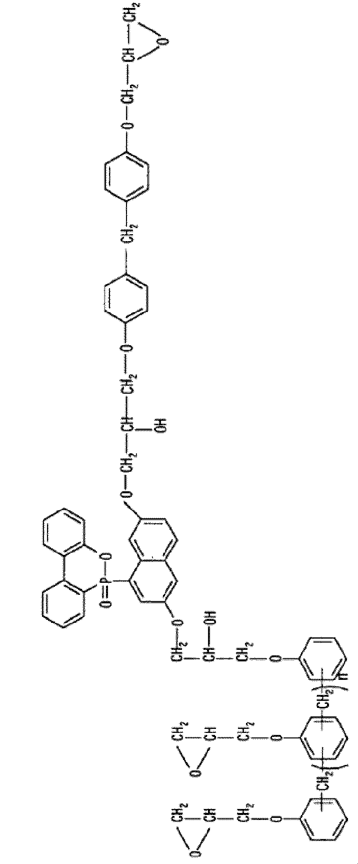
ここでリン含有難燃性エポキシ樹脂を用いる場合の樹脂組成物は、F成分としてのリン含有難燃性エポキシ樹脂の1種類を単独で用いても、2種類以上のリン含有難燃性エポキシ樹脂を混合して用いても構わない。但し、F成分としてのリン含有難燃性エポキシ樹脂の総量を考慮して、樹脂組成物重量を100重量%としたとき、F成分由来のリン原子を0.1重量%~5重量%の範囲となるように添加することが好ましい。リン含有難燃性エポキシ樹脂は、その種類によりエポキシ骨格内に含有するリン原子量が異なる。そこで、上述のようにリン原子の含有量を規定して、F成分の添加量に代えることが可能である。但し、F成分は、通常、樹脂組成物を100重量部としたとき、5重量部~50重量部の範囲で用いられる。F成分が5重量部未満の場合には、他の樹脂成分の配合割合を考慮すると、F成分由来のリン原子を0.1重量%以上とすることが困難になり、難燃性の向上効果を得ることが出来ない。一方、F成分が50重量部を超えるようにしても、難燃性向上効果も飽和すると同時に、硬化後の樹脂層が脆くなるため好ましくない。
上述の硬化樹脂層の「高Tg化」と「フレキシビリティ」とは、一般的に反比例する特性である。このときリン含有難燃性エポキシ樹脂は、硬化後の樹脂層のフレキシビリティの向上に寄与するもの、高Tg化に寄与するものが存在する。従って、1種類のリン含有難燃性エポキシ樹脂を用いるよりは、「高Tg化に寄与するリン含有難燃性エポキシ樹脂」と「フレキシビリティの向上に寄与するリン含有難燃性エポキシ樹脂」とをバランス良く配合して用いることで、フレキシブルプリント配線板用途で好適な樹脂組成物とすることが可能である。
本件発明に係る樹脂組成物は、更に、G成分として、エポキシ当量が200以下で、室温で液状のビスフェノールA型エポキシ樹脂、ビスフェノールF型エポキシ樹脂、ビスフェノールAD型エポキシ樹脂の群から選ばれる1種又は2種以上からなるエポキシ樹脂を含むものとしても良い。ここで、ビスフェノール系エポキシ樹脂を選択使用しているのは、C成分(ゴム変性ポリアミドイミド樹脂)との相性が良く、半硬化樹脂層に適度なフレキシビリティの付与が容易だからである。そして、エポキシ当量が200を超えると、樹脂が室温で半固形となり、半硬化状態でのフレキシビリティが減少するので好ましくない。更に、上述のビスフェノール系エポキシ樹脂であれば、1種を単独で用いても、2種以上を混合で用いても構わない。しかも、2種以上を混合して用いる場合には、その混合比に関しても特段の限定はない。
このG成分のエポキシ樹脂は、樹脂組成物を100重量部としたとき、2重量部~15重量部の配合割合で用いることが、熱硬化性を十分に発揮し、半硬化状態において、カールと呼ばれる反り現象の発生を低減させることが可能となり、また、半硬化状態での樹脂層のフレキシビリティの更なる向上を図ることができるため好ましい。当該エポキシ樹脂が15重量部を超えると、他の樹脂成分とのバランスから難燃性が低下したり、硬化後の樹脂層が硬くなる傾向がある。しかも、C成分(ゴム変性ポリアミドイミド樹脂)の添加量を考慮すると、硬化後の樹脂層として十分な靭性が得られなくなる。
本件発明に係る樹脂組成物は、更に、H成分として、熱可塑性樹脂及び/又は合成ゴムからなる低弾性物質を含むものとしても良い。H成分を含む樹脂組成物とすることにより、樹脂組成物の半硬化状態における割れを防ぎ、且つ硬化後のフレキシビリティを向上させることができる。このH成分としての低弾性物質は、例えば、アクリロニトリルブタジエンゴム、アクリルゴム(アクリル酸エステル共重合体)、ポリブタジエンゴム、イソプレン、水素添加型ポリブタジエン、ポリビニルブチラール、ポリエーテルサルフォン、フェノキシ、高分子エポキシ、芳香族ポリアミドが挙げられる。これらの中から1種を単独で用いても、2種以上を混合で用いても構わない。特に、アクリロニトリルブタジエンゴムを用いることが好ましい。アクリロニトリルブタジエンゴムの中でも、カルボキシル変性体であると、エポキシ樹脂と架橋構造を取り、硬化後の樹脂層のフレキシビリティを向上させることができる。カルボキシル変性体としては、カルボキシ基末端ニトリルブタジエンゴム(CTBN)、カルボキシ基末端ブタジエンゴム(CTB)、カルボキシ変性ニトリルブタジエンゴム(C-NBR)を用いることが好ましい。
H成分は、樹脂組成物を100重量部としたとき、25重量部以下の配合割合で用いることが好ましい。25重量部を超える量のH成分を加えると、ガラス転移温度Tgの低下、半田耐熱性能の低下、ピール強度の低下、熱膨張係数の増大といった問題が発生するため好ましくない。
本件発明に係る樹脂組成物は、上述のA成分~E成分を組み合わせることにより、難燃性の向上及びガラス転移温度Tgが高くなり、また、耐折性の熱劣化を防ぐことができる。そして、従来の接着剤用樹脂組成物のような無機充填剤を加えることなく、十分な屈曲性を得ることができる。さらに、半硬化状態での割れや打ち抜き加工時の粉落ちを防ぐことができる。
本件発明に係る樹脂ワニス: 本件発明に係る樹脂ワニスは、上述の樹脂組成物に溶剤を加えて、樹脂固形分量が30重量%~70重量%の範囲に調製したものである。そして、この樹脂ワニスにより形成する半硬化樹脂層は、MIL規格におけるMIL-P-13949Gに準拠して樹脂厚さを55μmとして測定したときのレジンフローが0%~10%の範囲にあることを特徴とする。ここで言う溶剤には、上述の沸点が50℃~200℃の範囲にある溶剤であるメチルエチルケトン、ジメチルアセトアミド、ジメチルホルムアミド等の群から選ばれる1種の単独溶剤又は2種以上の混合溶剤を用いることが好ましい。上述のように良好な半硬化樹脂層を得るためである。そして、ここに示した樹脂固形分量の範囲が、銅箔の表面に塗布したときに、最も膜厚を精度の良いものに制御できる範囲である。樹脂固形分が30重量%未満の場合には、粘度が低すぎて、銅箔表面への塗布直後に流れて膜厚均一性を確保しにくい。これに対して、樹脂固形分が70重量%を超えると、粘度が高くなり、銅箔表面への薄膜形成が困難となる。
当該樹脂ワニスは、これを用いて半硬化樹脂層を形成したとき、測定したレジンフローが0%~10%の範囲にあることが好ましい。当該レジンフローが高いと、樹脂付銅箔の樹脂層を用いて形成する絶縁層の厚さが不均一になる。しかし、本件発明に係る樹脂ワニスは、レジンフローを10%以下という低い値に抑えることができる。なお、本件発明に係る樹脂ワニスは、樹脂流れが殆ど生じないレベルが実現可能であるので、当該レジンフローの下限値を0%とした。なお、本件発明に係る樹脂ワニスのレジンフローのより好ましい範囲は0%~5%である。
本件明細書において、レジンフローとは、MIL規格におけるMIL-P-13949Gに準拠して、樹脂厚さを55μmとした樹脂付銅箔から10cm角試料を4枚サンプリングし、この4枚の試料を重ねた状態(積層体)でプレス温度171℃、プレス圧14kgf/cm2、プレス時間10分の条件で張り合わせ、そのときの樹脂流出重量を測定した結果から数1に基づいて算出した値である。
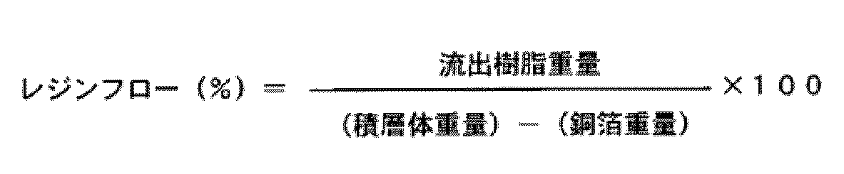
また、前記樹脂層は溶剤に可溶で且つ官能基として分子内に水酸基、カルボキシル基、アミノ基の1種又は2種以上を有するポリマー成分を2重量部~50重量部、沸点200℃以上のエポキシ樹脂及び沸点200℃以上のアミン系エポキシ樹脂硬化剤からなるエポキシ樹脂配合物を50重量部以上、を含有してもよい。前記樹脂層はフッ素樹脂基材またはフッ素樹脂フィルム接着用樹脂であってもよい。また、前記ポリマー成分は、ポリビニルアセタール樹脂、フェノキシ樹脂、芳香族ポリアミド樹脂、ポリエーテルサルホン樹脂、ポリアミドイミド樹脂の群から選ばれた1種又は2種以上を混合したものであってもよい。前記沸点200℃以上のエポキシ樹脂は、ビスフェノールA型エポキシ樹脂、ビスフェノールF型エポキシ樹脂、ゴム変性ビスフェノールA型エポキシ樹脂、ビフェニル型エポキシ樹脂の群から選ばれる1種又は2種以上を混合したものであってもよい。
前記アミン系エポキシ樹脂硬化剤は、芳香族ポリアミン、ポリアミド類及びこれらをエポキシ樹脂や多価カルボン酸と重合或いは縮合させて得られるアミンアダクト体の群から選ばれた1種又は2種以上を用いてもよい。
前記アミン系エポキシ樹脂硬化剤は、芳香族ポリアミン、ポリアミド類及びこれらをエポキシ樹脂や多価カルボン酸と重合或いは縮合させて得られるアミンアダクト体の群から選ばれた1種又は2種以上を用いてもよい。
なお、前記フッ素樹脂基材またはフッ素樹脂フィルムとは、PTFE(ポリテトラフルオロエチレン(4フッ化))、PFA(テトラフルオロエチレン・パーフルオロアルキルビニルエーテル共重合体)、FEP(テトラフルオロエチレン・ヘキサフルオロプロピレン共重合体(4.6フッ化))、ETFE(テトラフルオロエチレン・エチレン共重合体)、PVDF(ポリビニリデンフルオライド(2フッ化))、PCTFE(ポリクロロトリフルオロエチレン(3フッ化))、ポリアリルスルフォン、芳香族ポリスルフィドおよび芳香族ポリエーテルの中から選ばれるいずれか少なくとも1種の熱可塑性樹脂とフッ素樹脂とからなるフッ素系樹脂等を用いた基材またはフィルムであってもよい。ガラスクロス等の骨格材を含んでも含まなくとも構わない。また、このフッ素樹脂基材の厚さに関しても、特段の限定はない。
また、前記硬化剤としては、単に硬化させることのみを目的とすれば、ジシアンジアミド、イミダゾール類、芳香族アミン等のアミン類、ビスフェノールA、ブロム化ビスフェノールA等のフェノール類、フェノールノボラック樹脂及びクレゾールノボラック樹脂等のノボラック類、無水フタル酸等の酸無水物等のあらゆる硬化剤を用いることができる。これらの硬化剤はエポキシ樹脂に特に有効である。しかしながら、沸点200℃以上のアミン系エポキシ樹脂硬化剤を用いることが、フッ素樹脂基材と金属箔との密着性を顕著に向上させるという観点から最も好ましい。プレス成形温度が180℃付近であり、このプレス成形温度付近に硬化剤の沸点があると、プレス成形によりエポキシ樹脂硬化剤が沸騰するため硬化した絶縁樹脂層内に気泡が発生しやすくなる。そして、フッ素樹脂基材と金属箔との間に接着層を構成するのにアミン系エポキシ樹脂硬化剤を用いると最も安定した密着性が得られる。即ち、「沸点200℃以上のアミン系エポキシ樹脂硬化剤」とは、芳香族ポリアミン、ポリアミド類及びこれらをエポキシ樹脂や多価カルボン酸と重合或いは縮合させて得られるアミンアダクト体の群から選ばれた一種又は二種以上を用いる場合を言う。そして、これをより具体的に言えば、4,4’-ジアミノジフェニレンサルフォン、3,3’-ジアミノジフェニレンサルフォン、4,4-ジアミノジフェニレル、2,2-ビス[4-(4-アミノフェノキシ)フェニル]プロパン、ビス[4-(4-アミノフェノキシ)フェニル]サルフォンのいずれかを用いることが好ましい。また、当該アミン系エポキシ樹脂硬化剤のエポキシ樹脂に対する添加量は、それぞれの当量から自ずと導き出されるものであるため、本来厳密にその配合割合を明記する必要性はないものと考える。従って、本件発明では、硬化剤の添加量を特に限定していない。
また、必要に応じて適宜量添加する硬化促進剤を用いることも好ましい。ここで言う硬化促進剤とは、3級アミン、イミダゾール、尿素系硬化促進剤等である。本件発明では、この硬化促進剤の配合割合は、特に限定を設けていない。なぜなら、硬化促進剤は、プレス加工時の加熱条件等を考慮して、製造者が任意に選択的に添加量を定めて良いものであるからである。
そして、前記樹脂層はゴム性樹脂を含むことも好ましい。ここで言うゴム性樹脂とは、天然ゴム及び合成ゴムを含む概念として記載しており、後者の合成ゴムにはスチレン-ブタジエンゴム、ブタジエンゴム、ブチルゴム、エチレン-プロピレンゴム等がある。更に、耐熱性を要求される場合には、ニトリルゴム、クロロプレンゴム、シリコンゴム、ウレタンゴム等の耐熱性合成ゴムを選択使用することも有用である。これらのゴム性樹脂に関しては、上記ポリマー成分と反応して共重合体を形成するように、両末端に種々の官能基を備えるものであることが望ましい。
更に、上記高分子ポリマーの架橋剤を必要に応じて添加して用いることも好ましい。例えば、上記高分子ポリマーとして、ポリビニルアセタール樹脂を用いる場合には、ウレタン樹脂を架橋材として用いる等である。
前記樹脂層の樹脂組成物の構成成分は、樹脂組成物を100重量部としたとき、エポキシ樹脂が50重量部~80重量部、硬化剤が1重量部~15重量部、硬化促進剤が0.01重量部~1.0重量部、ポリマー成分が2重量部~50重量部、架橋剤が1重量部~5重量部、ゴム性樹脂が1重量部~10重量部の範囲の組成を採用してもよい。この組成範囲に含まれる限り、フッ素樹脂基材と金属箔との良好な密着性を維持し、且つ、製品の密着性のバラツキが少なくなる。
前記樹脂層は5~50重量部のエポキシ樹脂(硬化剤を含む)、50~95重量部のポリエーテルサルホン樹脂(末端に水酸基又はアミノ基を持ち且つ溶剤に可溶なもの)、及び、必要に応じて適宜量添加する硬化促進剤からなる樹脂混合物を用いて形成したものまたは当該樹脂混合物を半硬化させたものであってもよい。
前記樹脂層は銅箔側から順に第1熱硬化性樹脂層と、当該第1熱硬化性樹脂層の表面に位置する第2熱硬化性樹脂層とを有する樹脂層であって、第1熱硬化性樹脂層は、配線板製造プロセスにおけるデスミア処理時の薬品に溶解しない樹脂成分で形成されたものであり、第2熱硬化性樹脂層は、配線板製造プロセスにおけるデスミア処理時の薬品に溶解し洗浄除去可能な樹脂を用いて形成したものであってもよい。前記第1熱硬化性樹脂層は、ポリイミド樹脂、ポリエーテルサルホン、ポリフェニレンオキサイドのいずれか一種又は2種以上を混合した樹脂成分を用いて形成したものであってもよい。前記第2熱硬化性樹脂層は、エポキシ樹脂成分を用いて形成したものであってもよい。前記第1熱硬化性樹脂層の厚さt1(μm)は、キャリア付銅箔の粗化面粗さをRz(μm)とし、第2熱硬化性樹脂層の厚さをt2(μm)としたとき、t1は、Rz<t1<t2の条件を満たす厚さであることが好ましい。
前記樹脂層は骨格材に樹脂を含浸させたプリプレグであってもよい。前記骨格材に含浸させた樹脂は熱硬化性樹脂であることが好ましい。前記プリプレグは公知のプリプレグまたはプリント配線板製造に用いるプリプレグであってもよい。前記プリプレグは次の工程を有する製造方法により製造されたプリプレグであってもよい。1.液体状の熱硬化性樹脂を用いて、平坦なワーク平面の上に所定厚さの被膜として液体樹脂層を形成する液体樹脂被膜形成工程。2.ワーク平面上にある液体樹脂層を、そのままの状態で乾燥させることで乾燥樹脂層とする予備乾燥工程。3.ワーク平面上にある前記乾燥樹脂層の表面に、骨格材を重ね合わせ、予備加熱して圧着することで骨格材付乾燥樹脂層とする骨格材予備接着工程。4.ワーク平面上に骨格材付乾燥樹脂層を載置したまま、樹脂が再流動可能な温度で加熱し、当該骨格材に熱硬化性樹脂成分を含浸させる樹脂含浸工程。5.樹脂含浸が終了すると、熱硬化性樹脂を完全硬化させることなく、直ちに降温操作を行い、骨格材に含浸させた熱硬化性樹脂の半硬化状態を維持してプリプレグ状態となるようにする冷却工程。
前記骨格材はアラミド繊維又はガラス繊維又は全芳香族ポリエステル繊維を含んでもよい。前記骨格材はアラミド繊維又はガラス繊維又は全芳香族ポリエステル繊維の不織布若しくは織布であることが好ましい。また、前記全芳香族ポリエステル繊維は融点が300℃以上の全芳香族ポリエステル繊維であることが好ましい。前記融点が300℃以上の全芳香族ポリエステル繊維とは、所謂液晶ポリマーと称される樹脂を用いて製造される繊維であり、当該液晶ポリマーは2-ヒドロキシル-6-ナフトエ酸及びp-ヒドロキシ安息香酸の重合体を主成分とするものである。この全芳香族ポリエステル繊維は、低誘電率、低い誘電正接を持つため、電気的絶縁層の構成材として優れた性能を有し、ガラス繊維及びアラミド繊維と同様に使用することが可能なものである。
なお、前記不織布及び織布を構成する繊維は、その表面の樹脂との濡れ性を向上させるため、シランカップリング剤処理を施す事が好ましい。このときのシランカップリング剤は、使用目的に応じてアミノ系、エポキシ系等のシランカップリング剤を用いればよいのである。
なお、前記不織布及び織布を構成する繊維は、その表面の樹脂との濡れ性を向上させるため、シランカップリング剤処理を施す事が好ましい。このときのシランカップリング剤は、使用目的に応じてアミノ系、エポキシ系等のシランカップリング剤を用いればよいのである。
また、前記プリプレグは公称厚さが70μm以下のアラミド繊維又はガラス繊維を用いた不織布、あるいは、公称厚さが30μm以下のガラスクロスからなる骨格材に熱硬化性樹脂を含浸させたプリプレグであってもよい。
これらの樹脂を例えばメチルエチルケトン(MEK)、シクロペンタノン、ジメチルホルムアミド、ジメチルアセトアミド、N-メチルピロリドン、トルエン、メタノール、エタノール、プロピレングリコールモノメチルエーテル、ジメチルホルムアミド、ジメチルアセトアミド、シクロヘキサノン、エチルセロソルブ、N-メチル-2-ピロリドン、N,N-ジメチルアセトアミド、N,N-ジメチルホルムアミドなどの溶剤に溶解して樹脂液とし、これを前記極薄銅層上、あるいは前記耐熱層、防錆層、あるいは前記クロメート処理層、あるいは前記シランカップリング剤層の上に、例えばロールコータ法などによって塗布し、ついで必要に応じて加熱乾燥して溶剤を除去しBステージ状態にする。乾燥には例えば熱風乾燥炉を用いればよく、乾燥温度は100~250℃、好ましくは130~200℃であればよい。前記樹脂層の組成物を、溶剤を用いて溶解し、樹脂固形分3wt%~60wt%、好ましくは、10wt%~40wt%、より好ましくは25wt%~40wt%の樹脂液としてもよい。なお、メチルエチルケトンとシクロペンタノンとの混合溶剤を用いて溶解することが、環境的な見地より現段階では最も好ましい。
前記樹脂層を備えたキャリア付銅箔(樹脂付きキャリア付銅箔)は、その樹脂層を基材に重ね合わせたのち全体を熱圧着して該樹脂層を熱硬化せしめ、ついでキャリアを剥離して極薄銅層を表出せしめ(当然に表出するのは該極薄銅層の中間層側の表面である)、そこに所定の配線パターンを形成するという態様で使用される。
この樹脂付きキャリア付銅箔を使用すると、多層プリント配線基板の製造時におけるプリプレグ材の使用枚数を減らすことができる。しかも、樹脂層の厚みを層間絶縁が確保できるような厚みにしたり、プリプレグ材を全く使用していなくても銅張積層板を製造することができる。またこのとき、基材の表面に絶縁樹脂をアンダーコートして表面の平滑性を更に改善することもできる。
なお、プリプレグ材を使用しない場合には、プリプレグ材の材料コストが節約され、また積層工程も簡略になるので経済的に有利となり、しかも、プリプレグ材の厚み分だけ製造される多層プリント配線基板の厚みは薄くなり、1層の厚みが100μm以下である極薄の多層プリント配線基板を製造することができるという利点がある。
この樹脂層の厚みは0.1~120μmであることが好ましい。
樹脂層の厚みが0.1μmより薄くなると、接着力が低下し、プリプレグ材を介在させることなくこの樹脂付きキャリア付銅箔を内層材を備えた基材に積層したときに、内層材の回路との間の層間絶縁を確保することが困難になる場合がある。また、前記硬化樹脂層、半硬化樹脂層との総樹脂層厚みは0.1μm~120μmであるものが好ましく、35μm~120μmのものが実用上好ましい。そして、その場合の各厚みは、硬化樹脂層は5~20μmで、半硬化樹脂層は15~115μmであることが望ましい。総樹脂層厚みが120μmを超えると、薄厚の多層プリント配線板を製造することが難しくなる場合があり、35μm未満では薄厚の多層プリント配線板を形成し易くなるものの、内層の回路間における絶縁層である樹脂層が薄くなりすぎ、内層の回路間の絶縁性を不安定にする傾向が生じる場合があるためである。また、硬化樹脂層厚みが5μm未満であると、銅箔粗化面の表面粗度を考慮する必要が生じる場合がある。逆に硬化樹脂層厚みが20μmを超えると硬化済み樹脂層による効果は特に向上することがなくなる場合があり、総絶縁層厚は厚くなる。また、前記硬化樹脂層は、厚さが3μm~30μmであってもよい。また、前記半硬化樹脂層は、厚さが7μm~55μmであってもよい。また、前記硬化樹脂層と前記半硬化樹脂層との合計厚さは10μm~60μmであってもよい。
また、樹脂層を有するキャリア付銅箔が極薄の多層プリント配線板を製造することに用いられる場合には、前記樹脂層の厚みを0.1μm~5μm、より好ましくは0.5μm~5μm、より好ましくは1μm~5μmとすることが、多層プリント配線板の厚みを小さくするために好ましい。なお、前記樹脂層の厚みを0.1μm~5μmとする場合には、樹脂層とキャリア付銅箔との密着性を向上させるため、極薄銅層の上に耐熱層および/または防錆層および/またはクロメート処理層および/またはシランカップリング処理層を設けた後に、当該耐熱層または防錆層またはクロメート処理層またはシランカップリング処理層の上に樹脂層を形成することが好ましい。
また、樹脂層が誘電体を含む場合には、樹脂層の厚みは0.1~50μmであることが好ましく、0.5μm~25μmであることが好ましく、1.0μm~15μmであることがより好ましい。なお、前述の樹脂層の厚みは、任意の10点において断面観察により測定した厚みの平均値をいう。
また、樹脂層が誘電体を含む場合には、樹脂層の厚みは0.1~50μmであることが好ましく、0.5μm~25μmであることが好ましく、1.0μm~15μmであることがより好ましい。なお、前述の樹脂層の厚みは、任意の10点において断面観察により測定した厚みの平均値をいう。
一方、樹脂層の厚みを120μmより厚くすると、1回の塗布工程で目的厚みの樹脂層を形成することが困難となり、余分な材料費と工数がかかるため経済的に不利となる。更には、形成された樹脂層はその可撓性が劣るので、ハンドリング時にクラックなどが発生しやすくなり、また内層材との熱圧着時に過剰な樹脂流れが起こって円滑な積層が困難になる場合がある。
更に、この樹脂付きキャリア付銅箔のもう一つの製品形態としては、前記極薄銅層上、あるいは前記耐熱層、防錆層、あるいは前記クロメート処理層、あるいは前記シランカップリング処理層の上に樹脂層で被覆し、半硬化状態とした後、ついでキャリアを剥離して、キャリアが存在しない樹脂付き銅箔の形で製造することも可能である。
<5.キャリア付銅箔>
このようにして、銅箔キャリアと、銅箔キャリア上にNi層及びCr層がこの順に積層され、微量のZnを含有する中間層と、中間層の上に積層された極薄銅層とを備えたキャリア付銅箔が製造される。キャリア付銅箔自体の使用方法は当業者に周知であるが、例えば極薄銅層の表面を紙基材フェノール樹脂、紙基材エポキシ樹脂、合成繊維布基材エポキシ樹脂、ガラス布・紙複合基材エポキシ樹脂、ガラス布・ガラス不織布複合基材エポキシ樹脂及びガラス布基材エポキシ樹脂、ポリエステルフィルム、ポリイミドフィルム等の絶縁基板に貼り合わせて熱圧着後にキャリアを剥がし、絶縁基板に接着した極薄銅層を目的とする導体パターンにエッチングし、最終的にプリント配線板を製造することができる。更に、プリント配線板に電子部品類を搭載することで、プリント回路板が完成する。本発明に係るキャリア付銅箔の場合、剥離箇所は主としてCr層と極薄銅層の界面である。
このようにして、銅箔キャリアと、銅箔キャリア上にNi層及びCr層がこの順に積層され、微量のZnを含有する中間層と、中間層の上に積層された極薄銅層とを備えたキャリア付銅箔が製造される。キャリア付銅箔自体の使用方法は当業者に周知であるが、例えば極薄銅層の表面を紙基材フェノール樹脂、紙基材エポキシ樹脂、合成繊維布基材エポキシ樹脂、ガラス布・紙複合基材エポキシ樹脂、ガラス布・ガラス不織布複合基材エポキシ樹脂及びガラス布基材エポキシ樹脂、ポリエステルフィルム、ポリイミドフィルム等の絶縁基板に貼り合わせて熱圧着後にキャリアを剥がし、絶縁基板に接着した極薄銅層を目的とする導体パターンにエッチングし、最終的にプリント配線板を製造することができる。更に、プリント配線板に電子部品類を搭載することで、プリント回路板が完成する。本発明に係るキャリア付銅箔の場合、剥離箇所は主としてCr層と極薄銅層の界面である。
以下に、本発明に係るキャリア付銅箔を用いたプリント配線板の製造工程の例を幾つか示す。
本発明に係るプリント配線板の製造方法の一実施形態においては、本発明に係るキャリア付銅箔と絶縁基板とを準備する工程、前記キャリア付銅箔と絶縁基板を積層する工程、前記キャリア付銅箔と絶縁基板を極薄銅層側が絶縁基板と対向するように積層した後に、前記キャリア付銅箔のキャリアを剥がす工程を経て銅張積層板を形成し、その後、セミアディティブ法、モディファイドセミアディティブ法、パートリーアディティブ法及びサブトラクティブ法の何れかの方法によって、回路を形成する工程を含む。絶縁基板は内層回路入りのものとすることも可能である。
本発明において、セミアディティブ法とは、絶縁基板又は銅箔シード層上に薄い無電解めっきを行い、パターンを形成後、電気めっき及びエッチングを用いて導体パターンを形成する方法を指す。
従って、セミアディティブ法を用いた本発明に係るプリント配線板の製造方法の一実施形態においては、本発明に係るキャリア付銅箔と絶縁基板とを準備する工程、
前記キャリア付銅箔と絶縁基板を積層する工程、
前記キャリア付銅箔と絶縁基板を積層した後に、前記キャリア付銅箔のキャリアを剥がす工程、
前記キャリアを剥がして露出した極薄銅層を酸などの腐食溶液を用いたエッチングやプラズマなどの方法によりすべて除去する工程、
前記極薄銅層をエッチングにより除去することにより露出した前記樹脂にスルーホールまたは/およびブラインドビアを設ける工程、
前記スルーホールまたは/およびブラインドビアを含む領域についてデスミア処理を行う工程、
前記樹脂および前記スルーホールまたは/およびブラインドビアを含む領域について無電解めっき層を設ける工程、
前記無電解めっき層の上にめっきレジストを設ける工程、
前記めっきレジストに対して露光し、その後、回路が形成される領域のめっきレジストを除去する工程、
前記めっきレジストが除去された前記回路が形成される領域に、電解めっき層を設ける工程、
前記めっきレジストを除去する工程、
前記回路が形成される領域以外の領域にある無電解めっき層をフラッシュエッチングなどにより除去する工程、
を含む。
前記キャリア付銅箔と絶縁基板を積層する工程、
前記キャリア付銅箔と絶縁基板を積層した後に、前記キャリア付銅箔のキャリアを剥がす工程、
前記キャリアを剥がして露出した極薄銅層を酸などの腐食溶液を用いたエッチングやプラズマなどの方法によりすべて除去する工程、
前記極薄銅層をエッチングにより除去することにより露出した前記樹脂にスルーホールまたは/およびブラインドビアを設ける工程、
前記スルーホールまたは/およびブラインドビアを含む領域についてデスミア処理を行う工程、
前記樹脂および前記スルーホールまたは/およびブラインドビアを含む領域について無電解めっき層を設ける工程、
前記無電解めっき層の上にめっきレジストを設ける工程、
前記めっきレジストに対して露光し、その後、回路が形成される領域のめっきレジストを除去する工程、
前記めっきレジストが除去された前記回路が形成される領域に、電解めっき層を設ける工程、
前記めっきレジストを除去する工程、
前記回路が形成される領域以外の領域にある無電解めっき層をフラッシュエッチングなどにより除去する工程、
を含む。
セミアディティブ法を用いた本発明に係るプリント配線板の製造方法の別の一実施形態においては、本発明に係るキャリア付銅箔と絶縁基板とを準備する工程、
前記キャリア付銅箔と絶縁基板を積層する工程、
前記キャリア付銅箔と絶縁基板を積層した後に、前記キャリア付銅箔のキャリアを剥がす工程、
前記キャリアを剥がして露出した極薄銅層を酸などの腐食溶液を用いたエッチングやプラズマなどの方法によりすべて除去する工程、
前記極薄銅層をエッチングにより除去することにより露出した前記樹脂の表面について無電解めっき層を設ける工程、
前記無電解めっき層の上にめっきレジストを設ける工程、
前記めっきレジストに対して露光し、その後、回路が形成される領域のめっきレジストを除去する工程、
前記めっきレジストが除去された前記回路が形成される領域に、電解めっき層を設ける工程、
前記めっきレジストを除去する工程、
前記回路が形成される領域以外の領域にある無電解めっき層及び極薄銅層をフラッシュエッチングなどにより除去する工程、
を含む。
前記キャリア付銅箔と絶縁基板を積層する工程、
前記キャリア付銅箔と絶縁基板を積層した後に、前記キャリア付銅箔のキャリアを剥がす工程、
前記キャリアを剥がして露出した極薄銅層を酸などの腐食溶液を用いたエッチングやプラズマなどの方法によりすべて除去する工程、
前記極薄銅層をエッチングにより除去することにより露出した前記樹脂の表面について無電解めっき層を設ける工程、
前記無電解めっき層の上にめっきレジストを設ける工程、
前記めっきレジストに対して露光し、その後、回路が形成される領域のめっきレジストを除去する工程、
前記めっきレジストが除去された前記回路が形成される領域に、電解めっき層を設ける工程、
前記めっきレジストを除去する工程、
前記回路が形成される領域以外の領域にある無電解めっき層及び極薄銅層をフラッシュエッチングなどにより除去する工程、
を含む。
本発明において、モディファイドセミアディティブ法とは、絶縁層上に金属箔を積層し、めっきレジストにより非回路形成部を保護し、電解めっきにより回路形成部の銅厚付けを行った後、レジストを除去し、前記回路形成部以外の金属箔を(フラッシュ)エッチングで除去することにより、絶縁層上に回路を形成する方法を指す。
従って、モディファイドセミアディティブ法を用いた本発明に係るプリント配線板の製造方法の一実施形態においては、本発明に係るキャリア付銅箔と絶縁基板とを準備する工程、
前記キャリア付銅箔と絶縁基板を積層する工程、
前記キャリア付銅箔と絶縁基板を積層した後に、前記キャリア付銅箔のキャリアを剥がす工程、
前記キャリアを剥がして露出した極薄銅層と絶縁基板にスルーホールまたは/およびブラインドビアを設ける工程、
前記スルーホールまたは/およびブラインドビアを含む領域についてデスミア処理を行う工程、
前記スルーホールまたは/およびブラインドビアを含む領域について無電解めっき層を設ける工程、
前記キャリアを剥がして露出した極薄銅層表面にめっきレジストを設ける工程、
前記めっきレジストを設けた後に、電解めっきにより回路を形成する工程、
前記めっきレジストを除去する工程、
前記めっきレジストを除去することにより露出した極薄銅層をフラッシュエッチングにより除去する工程、
を含む。
前記キャリア付銅箔と絶縁基板を積層する工程、
前記キャリア付銅箔と絶縁基板を積層した後に、前記キャリア付銅箔のキャリアを剥がす工程、
前記キャリアを剥がして露出した極薄銅層と絶縁基板にスルーホールまたは/およびブラインドビアを設ける工程、
前記スルーホールまたは/およびブラインドビアを含む領域についてデスミア処理を行う工程、
前記スルーホールまたは/およびブラインドビアを含む領域について無電解めっき層を設ける工程、
前記キャリアを剥がして露出した極薄銅層表面にめっきレジストを設ける工程、
前記めっきレジストを設けた後に、電解めっきにより回路を形成する工程、
前記めっきレジストを除去する工程、
前記めっきレジストを除去することにより露出した極薄銅層をフラッシュエッチングにより除去する工程、
を含む。
モディファイドセミアディティブ法を用いた本発明に係るプリント配線板の製造方法の別の一実施形態においては、本発明に係るキャリア付銅箔と絶縁基板とを準備する工程、
前記キャリア付銅箔と絶縁基板を積層する工程、
前記キャリア付銅箔と絶縁基板を積層した後に、前記キャリア付銅箔のキャリアを剥がす工程、
前記キャリアを剥がして露出した極薄銅層の上にめっきレジストを設ける工程、
前記めっきレジストに対して露光し、その後、回路が形成される領域のめっきレジストを除去する工程、
前記めっきレジストが除去された前記回路が形成される領域に、電解めっき層を設ける工程、
前記めっきレジストを除去する工程、
前記回路が形成される領域以外の領域にある無電解めっき層及び極薄銅層をフラッシュエッチングなどにより除去する工程、
を含む。
前記キャリア付銅箔と絶縁基板を積層する工程、
前記キャリア付銅箔と絶縁基板を積層した後に、前記キャリア付銅箔のキャリアを剥がす工程、
前記キャリアを剥がして露出した極薄銅層の上にめっきレジストを設ける工程、
前記めっきレジストに対して露光し、その後、回路が形成される領域のめっきレジストを除去する工程、
前記めっきレジストが除去された前記回路が形成される領域に、電解めっき層を設ける工程、
前記めっきレジストを除去する工程、
前記回路が形成される領域以外の領域にある無電解めっき層及び極薄銅層をフラッシュエッチングなどにより除去する工程、
を含む。
本発明において、パートリーアディティブ法とは、導体層を設けてなる基板、必要に応じてスルーホールやバイアホール用の孔を穿けてなる基板上に触媒核を付与し、エッチングして導体回路を形成し、必要に応じてソルダレジストまたはメッキレジストを設けた後に、前記導体回路上、スルーホールやバイアホールなどに無電解めっき処理によって厚付けを行うことにより、プリント配線板を製造する方法を指す。
従って、パートリーアディティブ法を用いた本発明に係るプリント配線板の製造方法の一実施形態においては、本発明に係るキャリア付銅箔と絶縁基板とを準備する工程、
前記キャリア付銅箔と絶縁基板を積層する工程、
前記キャリア付銅箔と絶縁基板を積層した後に、前記キャリア付銅箔のキャリアを剥がす工程、
前記キャリアを剥がして露出した極薄銅層と絶縁基板にスルーホールまたは/およびブラインドビアを設ける工程、
前記スルーホールまたは/およびブラインドビアを含む領域についてデスミア処理を行う工程、
前記スルーホールまたは/およびブラインドビアを含む領域について触媒核を付与する工程、
前記キャリアを剥がして露出した極薄銅層表面にエッチングレジストを設ける工程、
前記エッチングレジストに対して露光し、回路パターンを形成する工程、
前記極薄銅層および前記触媒核を酸などの腐食溶液を用いたエッチングやプラズマなどの方法により除去して、回路を形成する工程、
前記エッチングレジストを除去する工程、
前記極薄銅層および前記触媒核を酸などの腐食溶液を用いたエッチングやプラズマなどの方法により除去して露出した前記絶縁基板表面に、ソルダレジストまたはメッキレジストを設ける工程、
前記ソルダレジストまたはメッキレジストが設けられていない領域に無電解めっき層を設ける工程、
を含む。
前記キャリア付銅箔と絶縁基板を積層する工程、
前記キャリア付銅箔と絶縁基板を積層した後に、前記キャリア付銅箔のキャリアを剥がす工程、
前記キャリアを剥がして露出した極薄銅層と絶縁基板にスルーホールまたは/およびブラインドビアを設ける工程、
前記スルーホールまたは/およびブラインドビアを含む領域についてデスミア処理を行う工程、
前記スルーホールまたは/およびブラインドビアを含む領域について触媒核を付与する工程、
前記キャリアを剥がして露出した極薄銅層表面にエッチングレジストを設ける工程、
前記エッチングレジストに対して露光し、回路パターンを形成する工程、
前記極薄銅層および前記触媒核を酸などの腐食溶液を用いたエッチングやプラズマなどの方法により除去して、回路を形成する工程、
前記エッチングレジストを除去する工程、
前記極薄銅層および前記触媒核を酸などの腐食溶液を用いたエッチングやプラズマなどの方法により除去して露出した前記絶縁基板表面に、ソルダレジストまたはメッキレジストを設ける工程、
前記ソルダレジストまたはメッキレジストが設けられていない領域に無電解めっき層を設ける工程、
を含む。
本発明において、サブトラクティブ法とは、銅張積層板上の銅箔の不要部分を、エッチングなどによって、選択的に除去して、導体パターンを形成する方法を指す。
従って、サブトラクティブ法を用いた本発明に係るプリント配線板の製造方法の一実施形態においては、本発明に係るキャリア付銅箔と絶縁基板とを準備する工程、
前記キャリア付銅箔と絶縁基板を積層する工程、
前記キャリア付銅箔と絶縁基板を積層した後に、前記キャリア付銅箔のキャリアを剥がす工程、
前記キャリアを剥がして露出した極薄銅層と絶縁基板にスルーホールまたは/およびブラインドビアを設ける工程、
前記スルーホールまたは/およびブラインドビアを含む領域についてデスミア処理を行う工程、
前記スルーホールまたは/およびブラインドビアを含む領域について無電解めっき層を設ける工程、
前記無電解めっき層の表面に、電解めっき層を設ける工程、
前記電解めっき層または/および前記極薄銅層の表面にエッチングレジストを設ける工程、
前記エッチングレジストに対して露光し、回路パターンを形成する工程、
前記極薄銅層および前記無電解めっき層および前記電解めっき層を酸などの腐食溶液を用いたエッチングやプラズマなどの方法により除去して、回路を形成する工程、
前記エッチングレジストを除去する工程、
を含む。
前記キャリア付銅箔と絶縁基板を積層する工程、
前記キャリア付銅箔と絶縁基板を積層した後に、前記キャリア付銅箔のキャリアを剥がす工程、
前記キャリアを剥がして露出した極薄銅層と絶縁基板にスルーホールまたは/およびブラインドビアを設ける工程、
前記スルーホールまたは/およびブラインドビアを含む領域についてデスミア処理を行う工程、
前記スルーホールまたは/およびブラインドビアを含む領域について無電解めっき層を設ける工程、
前記無電解めっき層の表面に、電解めっき層を設ける工程、
前記電解めっき層または/および前記極薄銅層の表面にエッチングレジストを設ける工程、
前記エッチングレジストに対して露光し、回路パターンを形成する工程、
前記極薄銅層および前記無電解めっき層および前記電解めっき層を酸などの腐食溶液を用いたエッチングやプラズマなどの方法により除去して、回路を形成する工程、
前記エッチングレジストを除去する工程、
を含む。
サブトラクティブ法を用いた本発明に係るプリント配線板の製造方法の別の一実施形態においては、本発明に係るキャリア付銅箔と絶縁基板とを準備する工程、
前記キャリア付銅箔と絶縁基板を積層する工程、
前記キャリア付銅箔と絶縁基板を積層した後に、前記キャリア付銅箔のキャリアを剥がす工程、
前記キャリアを剥がして露出した極薄銅層と絶縁基板にスルーホールまたは/およびブラインドビアを設ける工程、
前記スルーホールまたは/およびブラインドビアを含む領域についてデスミア処理を行う工程、
前記スルーホールまたは/およびブラインドビアを含む領域について無電解めっき層を設ける工程、
前記無電解めっき層の表面にマスクを形成する工程、
マスクが形成されいない前記無電解めっき層の表面に電解めっき層を設ける工程、
前記電解めっき層または/および前記極薄銅層の表面にエッチングレジストを設ける工程、
前記エッチングレジストに対して露光し、回路パターンを形成する工程、
前記極薄銅層および前記無電解めっき層を酸などの腐食溶液を用いたエッチングやプラズマなどの方法により除去して、回路を形成する工程、
前記エッチングレジストを除去する工程、
を含む。
前記キャリア付銅箔と絶縁基板を積層する工程、
前記キャリア付銅箔と絶縁基板を積層した後に、前記キャリア付銅箔のキャリアを剥がす工程、
前記キャリアを剥がして露出した極薄銅層と絶縁基板にスルーホールまたは/およびブラインドビアを設ける工程、
前記スルーホールまたは/およびブラインドビアを含む領域についてデスミア処理を行う工程、
前記スルーホールまたは/およびブラインドビアを含む領域について無電解めっき層を設ける工程、
前記無電解めっき層の表面にマスクを形成する工程、
マスクが形成されいない前記無電解めっき層の表面に電解めっき層を設ける工程、
前記電解めっき層または/および前記極薄銅層の表面にエッチングレジストを設ける工程、
前記エッチングレジストに対して露光し、回路パターンを形成する工程、
前記極薄銅層および前記無電解めっき層を酸などの腐食溶液を用いたエッチングやプラズマなどの方法により除去して、回路を形成する工程、
前記エッチングレジストを除去する工程、
を含む。
スルーホールまたは/およびブラインドビアを設ける工程、及びその後のデスミア工程は行わなくてもよい。
ここで、本発明のキャリア付銅箔を用いたプリント配線板の製造方法の具体例を図面を用いて詳細に説明する。なお、ここでは粗化処理層が形成された極薄銅層を有するキャリア付銅箔を例に説明するが、これに限られず、粗化処理層が形成されていない極薄銅層を有するキャリア付銅箔を用いても同様に下記のプリント配線板の製造方法を行うことができる。
まず、図1-Aに示すように、表面に粗化処理層が形成された極薄銅層を有するキャリア付銅箔(1層目)を準備する。
次に、図1-Bに示すように、極薄銅層の粗化処理層上にレジストを塗布し、露光・現像を行い、レジストを所定の形状にエッチングする。
次に、図1-Cに示すように、回路用のめっきを形成した後、レジストを除去することで、所定の形状の回路めっきを形成する。
次に、図2-Dに示すように、回路めっきを覆うように(回路めっきが埋没するように)極薄銅層上に埋め込み樹脂を設けて樹脂層を積層し、続いて別のキャリア付銅箔(2層目)を極薄銅層側から接着させる。
次に、図2-Eに示すように、2層目のキャリア付銅箔からキャリアを剥がす。
次に、図2-Fに示すように、樹脂層の所定位置にレーザー穴あけを行い、回路めっきを露出させてブラインドビアを形成する。
次に、図3-Gに示すように、ブラインドビアに銅を埋め込みビアフィルを形成する。
次に、図3-Hに示すように、ビアフィル上に、上記図1-B及び図1-Cのようにして回路めっきを形成する。
次に、図3-Iに示すように、1層目のキャリア付銅箔からキャリアを剥がす。
次に、図4-Jに示すように、フラッシュエッチングにより両表面の極薄銅層を除去し、樹脂層内の回路めっきの表面を露出させる。
次に、図4-Kに示すように、樹脂層内の回路めっき上にバンプを形成し、当該はんだ上に銅ピラーを形成する。このようにして本発明のキャリア付銅箔を用いたプリント配線板を作製する。
まず、図1-Aに示すように、表面に粗化処理層が形成された極薄銅層を有するキャリア付銅箔(1層目)を準備する。
次に、図1-Bに示すように、極薄銅層の粗化処理層上にレジストを塗布し、露光・現像を行い、レジストを所定の形状にエッチングする。
次に、図1-Cに示すように、回路用のめっきを形成した後、レジストを除去することで、所定の形状の回路めっきを形成する。
次に、図2-Dに示すように、回路めっきを覆うように(回路めっきが埋没するように)極薄銅層上に埋め込み樹脂を設けて樹脂層を積層し、続いて別のキャリア付銅箔(2層目)を極薄銅層側から接着させる。
次に、図2-Eに示すように、2層目のキャリア付銅箔からキャリアを剥がす。
次に、図2-Fに示すように、樹脂層の所定位置にレーザー穴あけを行い、回路めっきを露出させてブラインドビアを形成する。
次に、図3-Gに示すように、ブラインドビアに銅を埋め込みビアフィルを形成する。
次に、図3-Hに示すように、ビアフィル上に、上記図1-B及び図1-Cのようにして回路めっきを形成する。
次に、図3-Iに示すように、1層目のキャリア付銅箔からキャリアを剥がす。
次に、図4-Jに示すように、フラッシュエッチングにより両表面の極薄銅層を除去し、樹脂層内の回路めっきの表面を露出させる。
次に、図4-Kに示すように、樹脂層内の回路めっき上にバンプを形成し、当該はんだ上に銅ピラーを形成する。このようにして本発明のキャリア付銅箔を用いたプリント配線板を作製する。
上記別のキャリア付銅箔(2層目)は、本発明のキャリア付銅箔を用いてもよく、従来のキャリア付銅箔を用いてもよく、さらに通常の銅箔を用いてもよい。また、図3-Hに示される2層目の回路上に、さらに回路を1層或いは複数層形成してもよく、それらの回路形成をセミアディティブ法、サブトラクティブ法、パートリーアディティブ法又はモディファイドセミアディティブ法のいずれかの方法によって行ってもよい。
また、プリント配線板の製造時に、キャリア付銅箔のキャリアを補強するためのサポートをキャリア表面に貼付することも可能である。これにより取扱性を更に向上することができる。サポートとしてはプリプレグや樹脂等の絶縁基板が挙げられる。樹脂としては先述した樹脂層であってもよい。
本発明に係るキャリア付銅箔は、極薄銅層表面の色差が以下(1)~(4)いずれか1つ以上を満たすように制御されていることが好ましい。本発明において「極薄銅層表面の色差」とは、極薄銅層の表面の色差、又は、粗化処理等の各種表面処理が施されている場合はその表面処理層表面の色差を示す。すなわち、本発明に係るキャリア付銅箔は、極薄銅層または粗化処理層または耐熱層または防錆層またはクロメート処理層またはシランカップリング層の表面の色差が以下(1)~(4)いずれか1つ以上を満たすように制御されていることが好ましい。
(1)極薄銅層または粗化処理層または耐熱層または防錆層またはクロメート処理層またはシランカップリング処理層の表面のJISZ8730に基づく色差ΔLが-40以下である。
(2)極薄銅層または粗化処理層または耐熱層または防錆層またはクロメート処理層またはシランカップリング処理層の表面のJISZ8730に基づく色差ΔE*abが45以上である。
(3)極薄銅層または粗化処理層または耐熱層または防錆層またはクロメート処理層またはシランカップリング処理層の表面のJISZ8730に基づく色差Δaが20以下である。
(4)極薄銅層または粗化処理層または耐熱層または防錆層またはクロメート処理層またはシランカップリング処理層の表面のJISZ8730に基づく色差Δbが20以下である。
(1)極薄銅層または粗化処理層または耐熱層または防錆層またはクロメート処理層またはシランカップリング処理層の表面のJISZ8730に基づく色差ΔLが-40以下である。
(2)極薄銅層または粗化処理層または耐熱層または防錆層またはクロメート処理層またはシランカップリング処理層の表面のJISZ8730に基づく色差ΔE*abが45以上である。
(3)極薄銅層または粗化処理層または耐熱層または防錆層またはクロメート処理層またはシランカップリング処理層の表面のJISZ8730に基づく色差Δaが20以下である。
(4)極薄銅層または粗化処理層または耐熱層または防錆層またはクロメート処理層またはシランカップリング処理層の表面のJISZ8730に基づく色差Δbが20以下である。
ここで、上述の色差ΔL、Δa、Δbは、それぞれ色差計で測定され、黒/白/赤/緑/黄/青を加味し、JIS Z8730に基づくL*a*b表色系を用いて示される総合指標であり、ΔL:白黒、Δa:赤緑、Δb:黄青として表される。また、ΔE*abはこれらの色差を用いて下記式で表される。

上述の色差は、極薄銅層形成時の電流密度を高くし、メッキ液中の銅濃度を低くし、メッキ液の線流速を高くすることで調整することができる。
また上述の色差は、極薄銅層の表面に粗化処理を施して粗化処理層を設けることで調整することもできる。粗化処理層を設ける場合には銅およびニッケル、コバルト、タングステン、モリブデンからなる群から選択される一種以上の元素とを含む電界液を用いて、従来よりも電流密度を高く(例えば40~60A/dm2)し、処理時間を短く(例えば0.1~1.3秒)することで調整することができる。極薄銅層の表面に粗化処理層を設けない場合には、Niの濃度をその他の元素の2倍以上としたメッキ浴を用いて、極薄銅層または耐熱層または防錆層またはクロメート処理層またはシランカップリング処理層の表面にNi合金メッキ(例えばNi-W合金メッキ、Ni-Co-P合金メッキ、Ni-Zn合金めっき)を従来よりも低電流密度(0.1~1.3A/dm2)で処理時間を長く(20秒~40秒)設定して処理することで達成できる。
また上述の色差は、極薄銅層の表面に粗化処理を施して粗化処理層を設けることで調整することもできる。粗化処理層を設ける場合には銅およびニッケル、コバルト、タングステン、モリブデンからなる群から選択される一種以上の元素とを含む電界液を用いて、従来よりも電流密度を高く(例えば40~60A/dm2)し、処理時間を短く(例えば0.1~1.3秒)することで調整することができる。極薄銅層の表面に粗化処理層を設けない場合には、Niの濃度をその他の元素の2倍以上としたメッキ浴を用いて、極薄銅層または耐熱層または防錆層またはクロメート処理層またはシランカップリング処理層の表面にNi合金メッキ(例えばNi-W合金メッキ、Ni-Co-P合金メッキ、Ni-Zn合金めっき)を従来よりも低電流密度(0.1~1.3A/dm2)で処理時間を長く(20秒~40秒)設定して処理することで達成できる。
極薄銅層表面のJISZ8730に基づく色差ΔLが-40以下であると、例えば、キャリア付銅箔の極薄銅層表面に回路を形成する際に、極薄銅層と回路とのコントラストが鮮明となり、その結果、視認性が良好となり回路の位置合わせを精度良く行うことができる。極薄銅層表面のJISZ8730に基づく色差ΔLは、好ましくは-45以下であり、より好ましくは-50以下である。
極薄銅層表面のJISZ8730に基づく色差ΔE*abが45以上であると、例えば、キャリア付銅箔の極薄銅層表面に回路を形成する際に、極薄銅層と回路とのコントラストが鮮明となり、その結果、視認性が良好となり回路の位置合わせを精度良く行うことができる。極薄銅層表面のJISZ8730に基づく色差ΔE*abは、好ましくは50以上であり、より好ましくは55以上であり、更により好ましくは60以上である。
極薄銅層表面のJISZ8730に基づく色差Δaが20以下であると、例えば、キャリア付銅箔の極薄銅層表面に回路を形成する際に、極薄銅層と回路とのコントラストが鮮明となり、その結果、視認性がより良好となり回路の位置合わせを精度良く行うことができる。極薄銅層表面のJISZ8730に基づく色差Δaは、好ましくは15以下であり、より好ましくは10以下であり、更により好ましくは8以下である。
極薄銅層表面のJISZ8730に基づく色差Δbが20以下であると、例えば、キャリア付銅箔の極薄銅層表面に回路を形成する際に、極薄銅層と回路とのコントラストが鮮明となり、その結果、視認性がより良好となり回路の位置合わせを精度良く行うことができる。極薄銅層表面のJISZ8730に基づく色差Δbは、好ましくは15以下であり、より好ましくは10以下であり、更により好ましくは8以下である。
極薄銅層または粗化処理層または耐熱層または防錆層またはクロメート処理層またはシランカップリング層の表面の色差が上記のようの制御されている場合には、回路めっきとのコントラストが鮮明となり、視認性が良好となる。従って、上述のようなプリント配線板の例えば図1-Cに示すような製造工程において、回路めっきを精度良く所定の位置に形成することが可能となる。また、上述のようなプリント配線板の製造方法によれば、回路めっきが樹脂層に埋め込まれた構成となっているため、例えば図4-Jに示すようなフラッシュエッチングによる極薄銅層の除去の際に、回路めっきが樹脂層によって保護され、その形状が保たれ、これにより微細回路の形成が容易となる。また、回路めっきが樹脂層によって保護されるため、耐マイグレーション性が向上し、回路の配線の導通が良好に抑制される。このため、微細回路の形成が容易となる。また、図4-J及び図4-Kに示すようにフラッシュエッチングによって極薄銅層を除去したとき、回路めっきの露出面が樹脂層から凹んだ形状となるため、当該回路めっき上にバンプが、さらにその上に銅ピラーがそれぞれ形成しやすくなり、製造効率が向上する。
なお、埋め込み樹脂(レジン)には公知の樹脂、プリプレグを用いることができる。例えば、BT(ビスマレイミドトリアジン)レジンやBTレジンを含浸させたガラス布であるプリプレグ、味の素ファインテクノ株式会社製ABFフィルムやABFを用いることができる。また、前記埋め込み樹脂は熱硬化性樹脂を含んでもよく、熱可塑性樹脂であってもよい。また、前記埋め込み樹脂は熱可塑性樹脂を含んでもよい。前記埋め込み樹脂の種類は格別限定されるものではないが、例えば、エポキシ樹脂、ポリイミド樹脂、多官能性シアン酸エステル化合物、マレイミド化合物、ポリビニルアセタール樹脂、ウレタン樹脂、ブロック共重合ポリイミド樹脂、ブロック共重合ポリイミド樹脂、ポリエーテルサルホン、ポリエーテルスルホン樹脂、芳香族ポリアミド樹脂、ポリアミドイミド樹脂、ゴム変成エポキシ樹脂、フェノキシ樹脂、カルボキシル基変性アクリロニトリル-ブタジエン樹脂、ポリフェニレンオキサイド、ビスマレイミドトリアジン樹脂、熱硬化性ポリフェニレンオキサイド樹脂、シアネートエステル系樹脂、多価カルボン酸の無水物などを含む樹脂や、紙基材フェノール樹脂、紙基材エポキシ樹脂、合成繊維布基材エポキシ樹脂、ガラス布・紙複合基材エポキシ樹脂、ガラス布・ガラス不織布複合基材エポキシ樹脂及びガラス布基材エポキシ樹脂、ポリエステルフィルム、ポリイミドフィルム、液晶ポリマーフィルム、フッ素樹脂フィルムなどを好適なものとしてあげることができる。
以下に、本発明の実施例によって本発明をさらに詳しく説明するが、本発明は、これらの実施例によってなんら限定されるものではない。
1.キャリア付銅箔の製造
<No.1>
銅箔キャリアとして、厚さ35μmの長尺の電解銅箔(JX日鉱日石金属社製JTC)を用意した。この銅箔のシャイニー面に対して、以下の条件でロール・トウ・ロール型の連続めっきラインで電気めっきすることにより1000μg/dm2の付着量のNi層を形成した。
<No.1>
銅箔キャリアとして、厚さ35μmの長尺の電解銅箔(JX日鉱日石金属社製JTC)を用意した。この銅箔のシャイニー面に対して、以下の条件でロール・トウ・ロール型の連続めっきラインで電気めっきすることにより1000μg/dm2の付着量のNi層を形成した。
・Ni層(下地めっき)
硫酸ニッケル:270~280g/L
塩化ニッケル:35~45g/L
酢酸ニッケル:10~20g/L
クエン酸三ナトリウム:15~25g/L
光沢剤:サッカリン、ブチンジオール等
ドデシル硫酸ナトリウム:55~75ppm
pH:4~6
浴温:55~65℃
電流密度:7~11A/dm2
硫酸ニッケル:270~280g/L
塩化ニッケル:35~45g/L
酢酸ニッケル:10~20g/L
クエン酸三ナトリウム:15~25g/L
光沢剤:サッカリン、ブチンジオール等
ドデシル硫酸ナトリウム:55~75ppm
pH:4~6
浴温:55~65℃
電流密度:7~11A/dm2
水洗及び酸洗後、引き続き、ロール・トウ・ロール型の連続めっきライン上で、Ni層の上に11μg/dm2の付着量のCr層を以下の条件で電解クロメート処理することにより付着させた。
・電解クロメート処理
液組成:重クロム酸カリウム1~10g/L、亜鉛0g/L
pH:7~10
液温:40~60℃
電流密度:0.1~2.6A/dm2
クーロン量:0.5~30As/dm2
・電解クロメート処理
液組成:重クロム酸カリウム1~10g/L、亜鉛0g/L
pH:7~10
液温:40~60℃
電流密度:0.1~2.6A/dm2
クーロン量:0.5~30As/dm2
引き続き、ロール・トウ・ロール型の連続めっきライン上で、Cr層の上に厚み2~10μmの極薄銅層を以下の条件で電気めっきすることにより形成し、キャリア付銅箔を製造した。
・極薄銅層
銅濃度:30~120g/L
H2SO4濃度:20~120g/L
電解液温度:20~80℃
電流密度:10~100A/dm2
・極薄銅層
銅濃度:30~120g/L
H2SO4濃度:20~120g/L
電解液温度:20~80℃
電流密度:10~100A/dm2
<No.2~37>
No.1に対して、ライン速度を調整することによりNi付着量及びCr付着量を表1に記載の通り種々変更させた。また、Ni層形成時又はクロメート処理時に、Niめっき液又はクロメート処理液中に硫酸亜鉛(ZnSO4)の形態の亜鉛を添加し、亜鉛濃度:0.05~5g/Lの範囲で調整することにより、中間層のZn付着量を表1に記載の通り変化させた。但し、比較例15及び16は、亜鉛濃度をそれぞれ10g/L及び15g/Lとした。表中、下地めっきのところに「Ni」と表記されているのは、純ニッケルめっきを行ったことを意味し、「Ni-Zn」と表記されているのは、ニッケル亜鉛合金めっきを行ったことを意味する。また、表中、クロメート処理のところに「Cr」と表記されているのは、純クロメート処理を行ったことを意味し、「Zn-Cr」と表記されているのは、亜鉛クロメート処理を行ったことを意味する。このようにして、No.2~37のキャリア付銅箔を作製した。Ni付着量又はCr付着量が0の例はNiめっき又は電解クロメート処理を実施しなかったということである。なお、ニッケル亜鉛合金メッキ液またはクロメート処理液中の亜鉛濃度を高くすることで、Znの付着量を多くすることができる。また、クロメート処理液中のクロム濃度を高くすることで、Crの付着量を高くすることができる。
No.1に対して、ライン速度を調整することによりNi付着量及びCr付着量を表1に記載の通り種々変更させた。また、Ni層形成時又はクロメート処理時に、Niめっき液又はクロメート処理液中に硫酸亜鉛(ZnSO4)の形態の亜鉛を添加し、亜鉛濃度:0.05~5g/Lの範囲で調整することにより、中間層のZn付着量を表1に記載の通り変化させた。但し、比較例15及び16は、亜鉛濃度をそれぞれ10g/L及び15g/Lとした。表中、下地めっきのところに「Ni」と表記されているのは、純ニッケルめっきを行ったことを意味し、「Ni-Zn」と表記されているのは、ニッケル亜鉛合金めっきを行ったことを意味する。また、表中、クロメート処理のところに「Cr」と表記されているのは、純クロメート処理を行ったことを意味し、「Zn-Cr」と表記されているのは、亜鉛クロメート処理を行ったことを意味する。このようにして、No.2~37のキャリア付銅箔を作製した。Ni付着量又はCr付着量が0の例はNiめっき又は電解クロメート処理を実施しなかったということである。なお、ニッケル亜鉛合金メッキ液またはクロメート処理液中の亜鉛濃度を高くすることで、Znの付着量を多くすることができる。また、クロメート処理液中のクロム濃度を高くすることで、Crの付着量を高くすることができる。
2.キャリア付銅箔の特性評価
上記のようにして得られたキャリア付銅箔について、以下の方法で特性評価を実施した。結果を表1に示す。
<ピンホール>
民生用の写真用バックライトを光源にして、目視でピンホールの数を測定した。評価は以下の基準により行った。
×:ピンホール10,000個/dm2超
△:ピンホール5,000個/dm2以上~10,000個/dm2以下
○:ピンホール100個/dm2以上~5,000個/dm2未満
◎:ピンホール20個/dm2以上~100個/dm2未満
◎◎:ピンホール20個/dm2未満
<剥離強度(BTプレス後)>
キャリア付銅箔の極薄銅層側をBT基板と貼り合わせて温度195℃で2時間プレスした後、キャリア付銅箔のキャリア側を50mm/分の剥離速度、引き剥がし角度は90°でJIS C6471に準拠して剥離することによって剥離強度を測定した。結果を表1に示す。
上記のようにして得られたキャリア付銅箔について、以下の方法で特性評価を実施した。結果を表1に示す。
<ピンホール>
民生用の写真用バックライトを光源にして、目視でピンホールの数を測定した。評価は以下の基準により行った。
×:ピンホール10,000個/dm2超
△:ピンホール5,000個/dm2以上~10,000個/dm2以下
○:ピンホール100個/dm2以上~5,000個/dm2未満
◎:ピンホール20個/dm2以上~100個/dm2未満
◎◎:ピンホール20個/dm2未満
<剥離強度(BTプレス後)>
キャリア付銅箔の極薄銅層側をBT基板と貼り合わせて温度195℃で2時間プレスした後、キャリア付銅箔のキャリア側を50mm/分の剥離速度、引き剥がし角度は90°でJIS C6471に準拠して剥離することによって剥離強度を測定した。結果を表1に示す。
No.1は、中間層にZnを含有していないケースである。Ni及びCrの付着量が適切であったことから、実用可能な程度のピンホールの頻度及び剥離強度が得られた。しかしながら、Ni及びCrの付着量はNo.1と同程度として、中間層にZnを適切量添加したNo.2は、ピンホールの数が更に減少し、剥離強度がより適切な値へと上昇した。剥離強度は0.5~120g/cmの範囲が適切であり、0.5~30g/cmがより適切な範囲であり、1~30g/cmが更により適切な範囲であり、5~25g/cmが更に適切な範囲である。
その他の発明例においても、Ni及びCrの付着量が同等である参考例と比較することにより、ピンホールの頻度及び剥離強度の改善が図られていることが分かる。一方、No.15及び16はZn付着量が多すぎたことで、剥離強度が高すぎた。No.29~33は、Ni層又はCr層を形成しなかったことから、剥離不可となった。No.36~37はNiの付着量が多すぎたことで、密着力が不足し、連続めっきラインを走行している間に剥離が生じた。
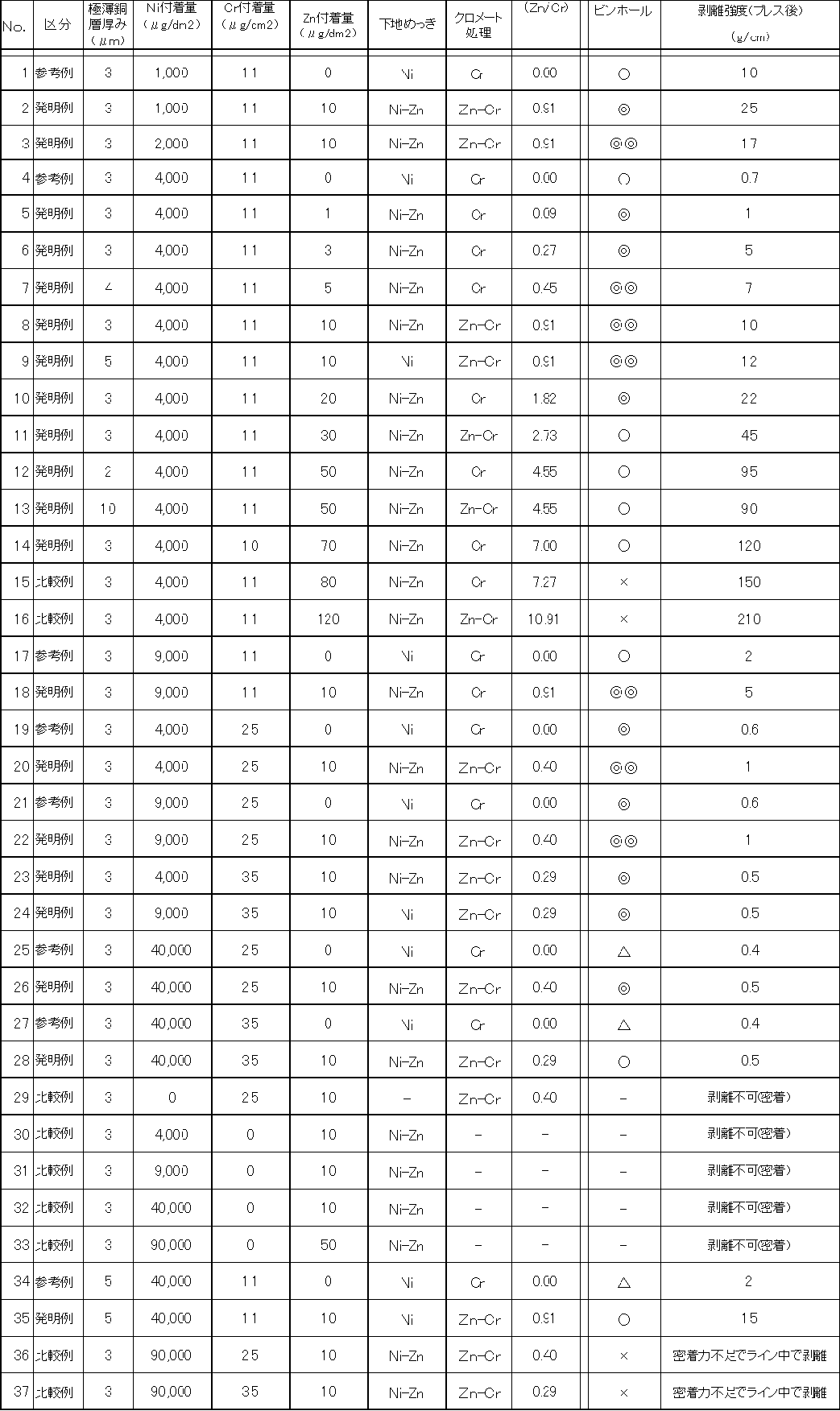
Claims (24)
- 銅箔キャリアと、銅箔キャリア上に積層された中間層と、中間層の上に積層された極薄銅層とを備えたキャリア付銅箔であって、中間層は銅箔キャリアとの界面に接しているNi層と極薄銅層との界面に接しているCr層で構成され、中間層におけるNiの付着量は1000~40000μg/dm2であり、中間層におけるCrの付着量は10~100μg/dm2であり、中間層には更に1~70μg/dm2の付着量でZnが存在するキャリア付銅箔。
- Niの付着量が2000~10000μg/dm2であり、Crの付着量が20~40μg/dm2である請求項1に記載のキャリア付銅箔。
- 中間層に存在するCrに対するZnの質量比の値が0.01~5の範囲である請求項1又は2に記載のキャリア付銅箔。
- Crは電解クロメートによって付着している請求項1~3の何れか一項に記載のキャリア付銅箔。
- 前記キャリアが電解銅箔又は圧延銅箔で形成されている請求項1~4の何れか一項に記載のキャリア付銅箔。
- 前記極薄銅層表面に粗化処理層を有する請求項1~5の何れか一項に記載のキャリア付銅箔。
- 前記粗化処理層が、銅、ニッケル、コバルト、リン、タングステン、ヒ素、モリブデン、クロム及び亜鉛からなる群から選択された何れかの単体又は何れか1種以上を含む合金からなる層である請求項6に記載のキャリア付銅箔。
- 前記粗化処理層の表面に、耐熱層、防錆層、クロメート処理層及びシランカップリング処理層からなる群から選択された1種以上の層を有する請求項6又は7に記載のキャリア付銅箔。
- 前記極薄銅層の表面に、耐熱層、防錆層、クロメート処理層及びシランカップリング処理層からなる群から選択された1種以上の層を有する請求項1~5の何れか一項に記載のキャリア付銅箔。
- 前記極薄銅層上に樹脂層を備える請求項1~5の何れか一項に記載のキャリア付銅箔。
- 前記粗化処理層上に樹脂層を備える請求項6~8の何れか一項に記載のキャリア付銅箔。
- 前記耐熱層、防錆層、クロメート処理層及びシランカップリング処理層からなる群から選択された1種以上の層の上に樹脂層を備える請求項9に記載のキャリア付銅箔。
- 前記樹脂層が接着用樹脂で形成されている請求項10~12の何れか一項に記載のキャリア付銅箔。
- 前記樹脂層が半硬化状態の樹脂で形成されている請求項10~13の何れか一項に記載のキャリア付銅箔。
- 前記樹脂層が誘電体を含む請求項10~14の何れか一項に記載のキャリア付銅箔。
- 請求項1~15の何れか一項に記載のキャリア付銅箔を用いて製造したプリント配線板。
- 請求項1~15の何れか一項に記載のキャリア付銅箔を用いて製造したプリント回路板。
- 請求項1~15の何れか一項に記載のキャリア付銅箔を用いて製造した銅張積層板。
- 請求項1~15の何れか一項に記載のキャリア付銅箔と絶縁基板とを準備する工程、
前記キャリア付銅箔と絶縁基板とを積層する工程、
前記キャリア付銅箔と絶縁基板とを積層した後に、前記キャリア付銅箔のキャリアを剥がす工程を経て銅張積層板を形成し、
その後、セミアディティブ法、サブトラクティブ法、パートリーアディティブ法又はモディファイドセミアディティブ法の何れかの方法によって、回路を形成する工程を含むプリント配線板の製造方法。 - 請求項1~15の何れか一項に記載のキャリア付銅箔の前記極薄銅層側表面に回路を形成する工程、
前記回路が埋没するように前記キャリア付銅箔の前記極薄銅層側表面に樹脂層を形成する工程、
前記樹脂層上に回路を形成する工程、
前記樹脂層上に回路を形成した後に、前記キャリアを剥離させる工程、及び、
前記キャリアを剥離させた後に、前記極薄銅層を除去することで、前記極薄銅層側表面に形成した、前記樹脂層に埋没している回路を露出させる工程
を含むプリント配線板の製造方法。 - 前記樹脂層上に回路を形成する工程が、前記樹脂層上に別のキャリア付銅箔を極薄銅層側から貼り合わせ、前記樹脂層に貼り合わせたキャリア付銅箔を用いて前記回路を形成する工程である請求項20に記載のプリント配線板の製造方法。
- 前記樹脂層上に貼り合わせる別のキャリア付銅箔が、請求項1~15の何れか一項に記載のキャリア付銅箔である請求項21に記載のプリント配線板の製造方法。
- 前記樹脂層上に回路を形成する工程が、セミアディティブ法、サブトラクティブ法、パートリーアディティブ法又はモディファイドセミアディティブ法の何れかの方法によって行われる請求項20~22の何れか一項に記載のプリント配線板の製造方法。
- 前記表面に回路を形成するキャリア付銅箔が、当該キャリア付銅箔のキャリアの表面に基板または樹脂層を有する請求項20~23の何れか一項に記載のプリント配線板の製造方法。
Applications Claiming Priority (2)
| Application Number | Priority Date | Filing Date | Title |
|---|---|---|---|
| JP2012-164714 | 2012-07-25 | ||
| JP2012164714A JP5156873B1 (ja) | 2012-07-25 | 2012-07-25 | キャリア付銅箔 |
Publications (1)
| Publication Number | Publication Date |
|---|---|
| WO2014017606A1 true WO2014017606A1 (ja) | 2014-01-30 |
Family
ID=48013527
Family Applications (1)
| Application Number | Title | Priority Date | Filing Date |
|---|---|---|---|
| PCT/JP2013/070231 Ceased WO2014017606A1 (ja) | 2012-07-25 | 2013-07-25 | キャリア付銅箔 |
Country Status (3)
| Country | Link |
|---|---|
| JP (1) | JP5156873B1 (ja) |
| TW (1) | TWI490113B (ja) |
| WO (1) | WO2014017606A1 (ja) |
Cited By (2)
| Publication number | Priority date | Publication date | Assignee | Title |
|---|---|---|---|---|
| WO2014200106A1 (ja) * | 2013-06-13 | 2014-12-18 | Jx日鉱日石金属株式会社 | キャリア付銅箔、銅張積層板、プリント配線板、電子機器、及び、プリント配線板の製造方法 |
| CN104943270A (zh) * | 2014-03-31 | 2015-09-30 | Jx日矿日石金属株式会社 | 附载体的铜箔、印刷布线板、层压体、电子机器及印刷布线板的制造方法 |
Families Citing this family (6)
| Publication number | Priority date | Publication date | Assignee | Title |
|---|---|---|---|---|
| JP5380615B1 (ja) * | 2012-10-26 | 2014-01-08 | Jx日鉱日石金属株式会社 | キャリア付銅箔、それを用いた銅張積層板、プリント配線板、プリント回路板、及び、プリント配線板の製造方法 |
| JP2014024315A (ja) * | 2012-12-07 | 2014-02-06 | Jx Nippon Mining & Metals Corp | キャリア付銅箔 |
| JP6254357B2 (ja) * | 2013-04-03 | 2017-12-27 | Jx金属株式会社 | キャリア付銅箔 |
| JP6246486B2 (ja) * | 2013-04-03 | 2017-12-13 | Jx金属株式会社 | キャリア付銅箔及びその製造方法、銅張積層板の製造方法及びプリント配線板の製造方法 |
| JP6426290B2 (ja) | 2015-07-23 | 2018-11-21 | 三井金属鉱業株式会社 | 樹脂付銅箔、銅張積層板及びプリント配線板 |
| TWI700393B (zh) | 2019-08-27 | 2020-08-01 | 長春石油化學股份有限公司 | 電解銅箔以及包含其之電極與鋰離子電池 |
Citations (5)
| Publication number | Priority date | Publication date | Assignee | Title |
|---|---|---|---|---|
| JPS6134385B2 (ja) * | 1980-07-14 | 1986-08-07 | Nippon Denkai Kk | |
| JP2000331537A (ja) * | 1999-05-19 | 2000-11-30 | Furukawa Circuit Foil Kk | 高密度超微細配線板用銅箔 |
| JP2001301087A (ja) * | 2000-03-10 | 2001-10-30 | Olin Corp | 低プロファイルの結合強化を施した銅箔 |
| JP2010006071A (ja) * | 2009-08-21 | 2010-01-14 | Furukawa Electric Co Ltd:The | 表面処理銅箔、キャリア付き極薄銅箔、フレキシブル銅張積層板及びポリイミド系フレキシブルプリント配線板 |
| WO2013031913A1 (ja) * | 2011-08-31 | 2013-03-07 | Jx日鉱日石金属株式会社 | キャリア付銅箔 |
Family Cites Families (2)
| Publication number | Priority date | Publication date | Assignee | Title |
|---|---|---|---|---|
| US6346335B1 (en) * | 2000-03-10 | 2002-02-12 | Olin Corporation | Copper foil composite including a release layer |
| US6893742B2 (en) * | 2001-02-15 | 2005-05-17 | Olin Corporation | Copper foil with low profile bond enhancement |
-
2012
- 2012-07-25 JP JP2012164714A patent/JP5156873B1/ja active Active
-
2013
- 2013-07-25 WO PCT/JP2013/070231 patent/WO2014017606A1/ja not_active Ceased
- 2013-07-25 TW TW102126636A patent/TWI490113B/zh active
Patent Citations (5)
| Publication number | Priority date | Publication date | Assignee | Title |
|---|---|---|---|---|
| JPS6134385B2 (ja) * | 1980-07-14 | 1986-08-07 | Nippon Denkai Kk | |
| JP2000331537A (ja) * | 1999-05-19 | 2000-11-30 | Furukawa Circuit Foil Kk | 高密度超微細配線板用銅箔 |
| JP2001301087A (ja) * | 2000-03-10 | 2001-10-30 | Olin Corp | 低プロファイルの結合強化を施した銅箔 |
| JP2010006071A (ja) * | 2009-08-21 | 2010-01-14 | Furukawa Electric Co Ltd:The | 表面処理銅箔、キャリア付き極薄銅箔、フレキシブル銅張積層板及びポリイミド系フレキシブルプリント配線板 |
| WO2013031913A1 (ja) * | 2011-08-31 | 2013-03-07 | Jx日鉱日石金属株式会社 | キャリア付銅箔 |
Cited By (6)
| Publication number | Priority date | Publication date | Assignee | Title |
|---|---|---|---|---|
| WO2014200106A1 (ja) * | 2013-06-13 | 2014-12-18 | Jx日鉱日石金属株式会社 | キャリア付銅箔、銅張積層板、プリント配線板、電子機器、及び、プリント配線板の製造方法 |
| JP5651811B1 (ja) * | 2013-06-13 | 2015-01-14 | Jx日鉱日石金属株式会社 | キャリア付銅箔、銅張積層板、プリント配線板、電子機器、及び、プリント配線板の製造方法 |
| CN105189829A (zh) * | 2013-06-13 | 2015-12-23 | Jx日矿日石金属株式会社 | 附载体的铜箔、覆铜积层板、印刷电路板、电子机器、及印刷电路板的制造方法 |
| CN105189829B (zh) * | 2013-06-13 | 2018-06-01 | Jx日矿日石金属株式会社 | 附载体的铜箔、覆铜积层板、印刷电路板、电子机器、及印刷电路板的制造方法 |
| CN104943270A (zh) * | 2014-03-31 | 2015-09-30 | Jx日矿日石金属株式会社 | 附载体的铜箔、印刷布线板、层压体、电子机器及印刷布线板的制造方法 |
| CN104943270B (zh) * | 2014-03-31 | 2017-10-31 | Jx日矿日石金属株式会社 | 附载体的铜箔、印刷布线板、层压体、电子机器及印刷布线板的制造方法 |
Also Published As
| Publication number | Publication date |
|---|---|
| JP2014027046A (ja) | 2014-02-06 |
| TWI490113B (zh) | 2015-07-01 |
| JP5156873B1 (ja) | 2013-03-06 |
| TW201422419A (zh) | 2014-06-16 |
Similar Documents
| Publication | Publication Date | Title |
|---|---|---|
| JP6475781B2 (ja) | 表面処理銅箔、キャリア付銅箔、基材の製造方法、プリント配線板の製造方法、プリント回路板の製造方法、銅張積層板 | |
| JP5544444B1 (ja) | 樹脂基材、プリント配線板、プリント回路板、銅張積層板及びプリント配線板の製造方法 | |
| JP5521099B1 (ja) | キャリア付銅箔、プリント配線板、プリント回路板、銅張積層板、及びプリント配線板の製造方法 | |
| JP2015078422A (ja) | キャリア付き銅箔 | |
| WO2014017606A1 (ja) | キャリア付銅箔 | |
| WO2014024994A1 (ja) | キャリア付銅箔 | |
| JP6310193B2 (ja) | キャリア付銅箔、その製造方法、銅張積層板の製造方法及びプリント配線板の製造方法 | |
| JP2015200026A (ja) | キャリア付銅箔、プリント配線板、積層体、積層板、電子機器及びプリント配線板の製造方法 | |
| WO2014084385A1 (ja) | キャリア付銅箔 | |
| JP6593979B2 (ja) | 表面処理銅箔、キャリア付銅箔、基材、銅張積層板の製造方法、電子機器の製造方法及びプリント配線板の製造方法 | |
| JP6310191B2 (ja) | キャリア付銅箔及びその製造方法、銅張積層板の製造方法及びプリント配線板の製造方法 | |
| JP2015009556A (ja) | キャリア付銅箔、その製造方法、プリント配線板、プリント回路板、銅張積層板及びプリント配線板の製造方法 | |
| JP2015200025A (ja) | キャリア付銅箔、プリント配線板、積層板、電子機器、積層体及びプリント配線板の製造方法 | |
| JP6335449B2 (ja) | キャリア付銅箔、銅張積層板の製造方法及びプリント配線板の製造方法 | |
| WO2014084384A1 (ja) | キャリア付銅箔 | |
| JP2016146477A (ja) | 表面処理銅箔、キャリア付銅箔、基材、樹脂基材、積層体、プリント配線板、電子機器の製造方法及びプリント配線板の製造方法 | |
| JP6415033B2 (ja) | キャリア付銅箔、銅張積層板の製造方法、及び、プリント配線板の製造方法 | |
| JP6377329B2 (ja) | キャリア付銅箔、銅張積層板の製造方法、及び、プリント配線板の製造方法 | |
| JP6273106B2 (ja) | キャリア付銅箔、銅張積層板の製造方法及びプリント配線板の製造方法 | |
| JP6310192B2 (ja) | キャリア付銅箔及びその製造方法、銅張積層板の製造方法及びプリント配線板の製造方法 | |
| WO2014084321A1 (ja) | キャリア付銅箔、キャリア付銅箔の製造方法、プリント配線板及びプリント回路板 | |
| JP2015078421A (ja) | キャリア付銅箔、キャリア付銅箔の製造方法、プリント配線板、プリント回路板、銅張積層板、及び、プリント配線板の製造方法 | |
| JP2015043419A (ja) | 樹脂基材、銅張積層板、プリント配線板、電子機器及びプリント配線板の製造方法 | |
| JP2015199354A (ja) | キャリア付銅箔、プリント配線板、積層体、積層板、電子機器及びプリント配線板の製造方法 | |
| JP2015199356A (ja) | キャリア付銅箔、プリント配線板、積層体、積層板、電子機器及びプリント配線板の製造方法 |
Legal Events
| Date | Code | Title | Description |
|---|---|---|---|
| 121 | Ep: the epo has been informed by wipo that ep was designated in this application |
Ref document number: 13822450 Country of ref document: EP Kind code of ref document: A1 |
|
| NENP | Non-entry into the national phase |
Ref country code: DE |
|
| 122 | Ep: pct application non-entry in european phase |
Ref document number: 13822450 Country of ref document: EP Kind code of ref document: A1 |