WO2014013864A1 - 上部電極、及びプラズマ処理装置 - Google Patents
上部電極、及びプラズマ処理装置 Download PDFInfo
- Publication number
- WO2014013864A1 WO2014013864A1 PCT/JP2013/068167 JP2013068167W WO2014013864A1 WO 2014013864 A1 WO2014013864 A1 WO 2014013864A1 JP 2013068167 W JP2013068167 W JP 2013068167W WO 2014013864 A1 WO2014013864 A1 WO 2014013864A1
- Authority
- WO
- WIPO (PCT)
- Prior art keywords
- electrode
- upper electrode
- plate
- plasma processing
- plasma
- Prior art date
- Legal status (The legal status is an assumption and is not a legal conclusion. Google has not performed a legal analysis and makes no representation as to the accuracy of the status listed.)
- Ceased
Links
Images



Classifications
-
- H—ELECTRICITY
- H01—ELECTRIC ELEMENTS
- H01J—ELECTRIC DISCHARGE TUBES OR DISCHARGE LAMPS
- H01J37/00—Discharge tubes with provision for introducing objects or material to be exposed to the discharge, e.g. for the purpose of examination or processing thereof
- H01J37/32—Gas-filled discharge tubes
- H01J37/32431—Constructional details of the reactor
- H01J37/32532—Electrodes
- H01J37/3255—Material
-
- C—CHEMISTRY; METALLURGY
- C23—COATING METALLIC MATERIAL; COATING MATERIAL WITH METALLIC MATERIAL; CHEMICAL SURFACE TREATMENT; DIFFUSION TREATMENT OF METALLIC MATERIAL; COATING BY VACUUM EVAPORATION, BY SPUTTERING, BY ION IMPLANTATION OR BY CHEMICAL VAPOUR DEPOSITION, IN GENERAL; INHIBITING CORROSION OF METALLIC MATERIAL OR INCRUSTATION IN GENERAL
- C23C—COATING METALLIC MATERIAL; COATING MATERIAL WITH METALLIC MATERIAL; SURFACE TREATMENT OF METALLIC MATERIAL BY DIFFUSION INTO THE SURFACE, BY CHEMICAL CONVERSION OR SUBSTITUTION; COATING BY VACUUM EVAPORATION, BY SPUTTERING, BY ION IMPLANTATION OR BY CHEMICAL VAPOUR DEPOSITION, IN GENERAL
- C23C4/00—Coating by spraying the coating material in the molten state, e.g. by flame, plasma or electric discharge
- C23C4/04—Coating by spraying the coating material in the molten state, e.g. by flame, plasma or electric discharge characterised by the coating material
-
- C—CHEMISTRY; METALLURGY
- C23—COATING METALLIC MATERIAL; COATING MATERIAL WITH METALLIC MATERIAL; CHEMICAL SURFACE TREATMENT; DIFFUSION TREATMENT OF METALLIC MATERIAL; COATING BY VACUUM EVAPORATION, BY SPUTTERING, BY ION IMPLANTATION OR BY CHEMICAL VAPOUR DEPOSITION, IN GENERAL; INHIBITING CORROSION OF METALLIC MATERIAL OR INCRUSTATION IN GENERAL
- C23C—COATING METALLIC MATERIAL; COATING MATERIAL WITH METALLIC MATERIAL; SURFACE TREATMENT OF METALLIC MATERIAL BY DIFFUSION INTO THE SURFACE, BY CHEMICAL CONVERSION OR SUBSTITUTION; COATING BY VACUUM EVAPORATION, BY SPUTTERING, BY ION IMPLANTATION OR BY CHEMICAL VAPOUR DEPOSITION, IN GENERAL
- C23C4/00—Coating by spraying the coating material in the molten state, e.g. by flame, plasma or electric discharge
- C23C4/04—Coating by spraying the coating material in the molten state, e.g. by flame, plasma or electric discharge characterised by the coating material
- C23C4/10—Oxides, borides, carbides, nitrides or silicides; Mixtures thereof
- C23C4/11—Oxides
-
- H—ELECTRICITY
- H01—ELECTRIC ELEMENTS
- H01J—ELECTRIC DISCHARGE TUBES OR DISCHARGE LAMPS
- H01J37/00—Discharge tubes with provision for introducing objects or material to be exposed to the discharge, e.g. for the purpose of examination or processing thereof
- H01J37/32—Gas-filled discharge tubes
- H01J37/32431—Constructional details of the reactor
- H01J37/3244—Gas supply means
-
- H—ELECTRICITY
- H01—ELECTRIC ELEMENTS
- H01J—ELECTRIC DISCHARGE TUBES OR DISCHARGE LAMPS
- H01J37/00—Discharge tubes with provision for introducing objects or material to be exposed to the discharge, e.g. for the purpose of examination or processing thereof
- H01J37/32—Gas-filled discharge tubes
- H01J37/32431—Constructional details of the reactor
- H01J37/32532—Electrodes
-
- H—ELECTRICITY
- H01—ELECTRIC ELEMENTS
- H01J—ELECTRIC DISCHARGE TUBES OR DISCHARGE LAMPS
- H01J37/00—Discharge tubes with provision for introducing objects or material to be exposed to the discharge, e.g. for the purpose of examination or processing thereof
- H01J37/32—Gas-filled discharge tubes
- H01J37/32431—Constructional details of the reactor
- H01J37/32532—Electrodes
- H01J37/32568—Relative arrangement or disposition of electrodes; moving means
-
- C—CHEMISTRY; METALLURGY
- C23—COATING METALLIC MATERIAL; COATING MATERIAL WITH METALLIC MATERIAL; CHEMICAL SURFACE TREATMENT; DIFFUSION TREATMENT OF METALLIC MATERIAL; COATING BY VACUUM EVAPORATION, BY SPUTTERING, BY ION IMPLANTATION OR BY CHEMICAL VAPOUR DEPOSITION, IN GENERAL; INHIBITING CORROSION OF METALLIC MATERIAL OR INCRUSTATION IN GENERAL
- C23C—COATING METALLIC MATERIAL; COATING MATERIAL WITH METALLIC MATERIAL; SURFACE TREATMENT OF METALLIC MATERIAL BY DIFFUSION INTO THE SURFACE, BY CHEMICAL CONVERSION OR SUBSTITUTION; COATING BY VACUUM EVAPORATION, BY SPUTTERING, BY ION IMPLANTATION OR BY CHEMICAL VAPOUR DEPOSITION, IN GENERAL
- C23C4/00—Coating by spraying the coating material in the molten state, e.g. by flame, plasma or electric discharge
- C23C4/12—Coating by spraying the coating material in the molten state, e.g. by flame, plasma or electric discharge characterised by the method of spraying
Definitions
- Various aspects and embodiments of the present invention relate to an upper electrode and a plasma processing apparatus.
- plasma processing apparatuses that perform plasma processing for the purpose of thin film deposition or etching are widely used.
- the plasma processing apparatus include a plasma CVD (Chemical Vapor Deposition) apparatus that performs a thin film deposition process, a plasma etching apparatus that performs an etching process, and the like.
- the plasma processing apparatus is, for example, disposed in a processing container that defines a plasma processing space, a mounting table in which a substrate to be processed is installed in the processing container, and a mounting table that faces the mounting table through the plasma processing space, and has conductivity.
- An upper electrode including an electrode plate is provided.
- the upper part of the member is relatively high in thermal conductivity in order to suppress the temperature rise.
- electrode plates for electrodes For example, in Patent Document 1, a plate-like member in which a process gas flow path for plasma processing is formed is formed of a conductive material having high thermal conductivity, and the surface of the flow path of the plate-like member on the outlet side is formed.
- the electrode plate is cooled by detachably installing the electrode plate of the upper electrode.
- the conventional technology it is difficult to maintain the uniformity of the temperature of the upper electrode. That is, in the prior art, since the electrode plate is detachably installed on the surface on the outlet side of the flow path of the plate-like member in which the process gas flow path is formed, the electrode plate is bent by its own weight. A gap is generated between the plate member and the electrode plate, so that heat is hardly transmitted from the electrode plate to the plate member. As a result, in the prior art, the temperature uniformity of the upper electrode may be impaired.
- the upper electrode includes a plate member and an electrode portion.
- the plate-like member is formed with a flow path through which a processing gas used for plasma processing flows.
- the electrode portion is formed in a film shape by spraying silicon on the surface of the plate-like member on the outlet side of the flow path.
- an upper electrode capable of maintaining temperature uniformity of the upper electrode and a plasma processing apparatus are realized.
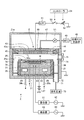
- FIG. 1 is a longitudinal sectional view showing an outline of a configuration of a plasma processing apparatus according to an embodiment.
- FIG. 2 is a longitudinal sectional view of an upper electrode according to an embodiment.
- FIG. 3 is a longitudinal sectional view of Modification 1 of the upper electrode according to the embodiment.
- FIG. 4 is a longitudinal sectional view of Modification 2 of the upper electrode according to the embodiment.
- FIG. 5 is a longitudinal sectional view of Modification 3 of the upper electrode according to the embodiment.
- FIG. 6 is a longitudinal sectional view of Modification 4 of the upper electrode according to the embodiment.
- FIG. 7 is a longitudinal sectional view of Modification 5 of the upper electrode according to the embodiment.
- FIG. 8 is a longitudinal sectional view of Modification 6 of the upper electrode according to the embodiment.
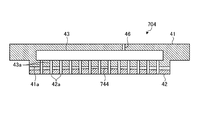
- FIG. 9 is a longitudinal sectional view of Modification 7 of the upper electrode according to the embodiment.
- FIG. 1 is a longitudinal sectional view showing an outline of a configuration of a plasma processing apparatus according to an embodiment.
- the plasma processing apparatus 2 is configured as a capacitively coupled parallel plate plasma etching apparatus, and has a processing chamber 21 that is a processing container that defines a plasma processing space for performing plasma processing.
- a support base 23 is disposed at the bottom of the processing chamber 21 which is a processing container via an insulating plate 22 made of ceramics or the like.
- a susceptor 24 made of, for example, aluminum and constituting a lower electrode is provided on the support base 23.
- An electrostatic chuck 25 that attracts and holds a wafer W as a substrate to be processed by electrostatic force is provided at the upper center of the susceptor 24.
- the electrostatic chuck 25 has a structure in which an electrode 26 made of a conductive film is sandwiched between a pair of insulating layers.
- a DC power source 27 is electrically connected to the electrode 26.
- a conductive focus ring (correction ring) 25a made of, for example, silicon is disposed on the susceptor 24 so as to surround the electrostatic chuck 25 in order to improve etching uniformity.
- reference numeral 28 denotes a cylindrical inner wall member made of, for example, quartz, and is provided so as to surround the susceptor 24 and the support base 23.
- a refrigerant chamber 29 is provided along the circumferential direction of the support base 23.
- a coolant having a predetermined temperature for example, cooling water
- a chiller unit (not shown) provided outside through the pipes 30a and 30b
- the processing temperature of the wafer W on the susceptor 24 depends on the coolant temperature.
- a heat transfer gas such as He gas from a heat transfer gas supply mechanism (not shown) is supplied between the upper surface of the electrostatic chuck 25 and the back surface of the wafer W via the gas supply line 31.
- the upper electrode 4 is provided above the susceptor 24, which is the lower electrode, so as to face the susceptor 24 through the plasma processing space of the processing chamber 21.
- a space between the upper electrode 4 and the susceptor 24 becomes a plasma processing space for generating plasma.
- FIG. 2 is a longitudinal sectional view of an upper electrode according to an embodiment.
- the upper electrode 4 includes a plate-like member 41 as an electrode main body portion and an electrode portion 42.
- the plate-like member 41 is supported on the upper part of the processing chamber 21 via the insulating shielding member 45.
- the plate-like member 41 is an electrode that is formed into a disc shape by a conductive material having a relatively high thermal conductivity, such as aluminum whose surface is anodized, and is heated by plasma generated in the plasma treatment space. It functions as a cooling plate that cools the portion 42.
- a gas introduction port 46 for introducing a processing gas for plasma processing, a gas diffusion chamber 43 for diffusing the processing gas introduced from the gas introduction port 46, and the gas diffusion chamber 43 are dispersed. Gas flow holes 43a, which are flow paths through which the processing gas flows, are formed.
- the electrode part 42 is formed in a film shape by thermal spraying of silicon on the surface 41a on the outlet side of the gas flow hole 43a of the plate-like member 41.
- the electrode portion 42 is formed in a film shape by spraying silicon on the surface 41 a on the outlet side of the gas flow hole 43 a of the plate member 41, and the shape of the plate member 41 is formed. It is formed in a disk shape corresponding to.
- a plasma spraying method is used as a silicon spraying method.
- an inert gas in a nozzle is energized to generate a plasma flow, a sprayed material such as powdered silicon is injected into the generated plasma flow, and the plasma flow into which the sprayed material is charged is discharged from the nozzle.
- a sprayed material such as powdered silicon
- the plasma flow into which the sprayed material is charged is discharged from the nozzle.
- This is a film forming technique for forming a film by spraying on a workpiece.
- Plasma spraying has the property that the adhesion between the workpiece and the film is relatively high.
- the coating formed by the plasma spraying method has characteristics of high hardness, strong adhesion between particles, high density, and a smooth shape.
- the plasma spraying method also has a characteristic that the thermal distortion of the workpiece is small and deterioration of the workpiece can be suppressed.
- the electrode portion 42 is formed with a gas introduction hole 42a that penetrates the electrode portion 42 in the thickness direction.
- the gas introduction holes 42 a are arranged so as to overlap the outlets of the gas flow holes 43 a of the plate-like member 41. As a result, the processing gas supplied to the gas diffusion chamber 43 is dispersed and supplied into the processing chamber 21 through the gas flow holes 43a and the gas introduction holes 42a.
- the concentration of boron (boron) added to silicon is adjusted at the peripheral portion of the electrode portion 42 and the central portion of the electrode portion 42.
- the specific resistance of the peripheral portion of the electrode portion 42 and the specific resistance of the central portion of the electrode portion 42 are set to different values.
- the specific resistance of the peripheral portion of the electrode portion 42 and the specific resistance of the central portion of the electrode portion 42 are set to different values in the range of 0.01 m ⁇ cm to 100 ⁇ cm.
- the specific resistance of the central portion of the electrode portion 42 is adjusted by adjusting the concentration of boron in silicon in the central portion of the electrode portion 42 to a value larger than the concentration of boron in silicon in the peripheral portion of the electrode portion 42. It is set to a value larger than the specific resistance of the peripheral portion of the electrode portion 42. Thereby, the impedance of the center part of the electrode part 42 with respect to plasma becomes larger than the peripheral part of the electrode part 42.
- the specific resistance of the central portion of the electrode portion 42 is adjusted by adjusting the concentration of boron in silicon in the central portion of the electrode portion 42 to a value smaller than the concentration of boron in silicon in the peripheral portion of the electrode portion 42. Is set to a value smaller than the specific resistance of the peripheral portion of the electrode portion 42. Thereby, the impedance of the central part of the electrode part 42 with respect to plasma becomes smaller than the peripheral part of the electrode part 42.
- a gas supply pipe 47 is connected to the gas inlet 46 of the plate member 41.
- a processing gas supply source 48 is connected to the gas supply pipe 47.
- the gas supply pipe 47 is provided with a mass flow controller (MFC) 49 and an opening / closing valve V1 in order from the upstream side.
- a gas such as a fluorocarbon gas (CxFy) such as C 4 F 8 gas is supplied from the processing gas supply source 48 to the gas diffusion chamber 43 through the gas supply pipe 47 as a processing gas for etching, for example. Thereafter, it is supplied into the processing chamber 21.
- the gas supply pipe 47, the processing gas supply source 48, and the upper electrode 4 constitute a processing gas supply unit.
- a variable DC power source 52 is electrically connected to the upper electrode 4 via a low pass filter (LPF) 51.
- the variable DC power supply 52 can be turned on / off by an on / off switch 53.
- the controller 54 controls the current / voltage of the variable DC power supply 52 and the on / off of the on / off switch 53.
- the on / off switch 53 When a high frequency is applied from the first and second high frequency power sources 62 and 64 to the susceptor 24 to generate plasma in the plasma processing space, the on / off switch 53 is turned on via the controller 54 and the upper electrode 4 is turned on. A predetermined direct current negative voltage is applied to.
- a cylindrical ground conductor 21 a is provided so as to extend upward from the side wall of the processing chamber 21 above the height position of the upper electrode 4.
- the ground conductor 21a has a top wall at the top thereof.
- a first high frequency power supply 62 is electrically connected to the susceptor 24, which is the lower electrode, via a matching unit 61.
- a second high frequency power supply 64 is connected to the susceptor 24 via a matching unit 63.
- the first high frequency power supply 62 has a role of generating a plasma in a plasma processing space between the upper electrode 4 and the susceptor 24 by outputting a high frequency power of 27 MHz or higher, for example, 40 MHz. Etching is performed on the wafer W by the plasma generated in the plasma processing space.
- the second high frequency power supply 64 has a role of drawing ion species generated by outputting high frequency power of 13.56 MHz or less, for example, 2 MHz, into the wafer W held by the electrostatic chuck.
- An exhaust port 71 is provided at the bottom of the processing chamber 21, and an exhaust device 73 that is an exhaust unit is connected to the exhaust port 71 via an exhaust pipe 72.
- the exhaust device 73 has a vacuum pump, for example, and can reduce the inside of the processing chamber 21 to a desired vacuum pressure.
- a loading / unloading port 74 for the wafer W is provided on the side wall of the processing chamber 21, and the loading / unloading port 74 can be opened and closed by a gate valve 75.
- 76 and 77 are deposition shields, and the deposition shield 76 is provided along the inner wall surface of the processing chamber 21, and has a role of preventing etching by-products (depots) from adhering to the processing chamber 21. It is detachably provided on the inner wall surface.
- a conductive member (GND block) 79 connected to the ground in a DC manner is provided at substantially the same height position as the wafer W in the portion constituting the inner wall of the processing chamber 21 of the deposition shield 76. Discharge is prevented.
- the electrode member 42 and the electrode are formed by spraying silicon on the surface 41a on the outlet side of the gas flow hole 43a of the plate member 41 to form the electrode portion 42 in a film shape. It is possible to avoid a situation in which a gap serving as a thermal resistance occurs between the portion 42 and the portion 42. As a result, according to the present embodiment, the uniformity of the temperature of the upper electrode 4 including the plate-like member 41 and the electrode portion 42 can be maintained, so that the entire surface to be processed of the wafer W is uniform. Plasma treatment can be performed.
- the electrode portion 42 of the upper electrode 4 is worn by being damaged by the plasma.
- the electrode part 42 is formed in a film shape by spraying silicon on the surface 41a on the outlet side of the gas flow hole 43a of the plate-like member 41, the electrode part 42 of the upper electrode 4 is formed. Even when the electrode is consumed, the silicon can be sprayed again to easily form the electrode portion 42 into a film shape. As a result, according to the present embodiment, it is possible to make it unnecessary to replace the entire upper electrode 4, and thus it is possible to suppress an increase in cost associated with the replacement.
- the specific resistance of the peripheral part of the electrode part 42 and the specific resistance of the central part of the electrode part 42 are set to different values, thereby appropriately controlling the impedance of the electrode part 42 with respect to plasma. can do.
- uniform plasma processing can be performed on the entire processing target surface of the wafer W.
- silicone is adjusted with the peripheral part of the electrode part 42, and the center part of the electrode part 42, and the specific resistance of the peripheral part of the electrode part 42 and the electrode part 42 are adjusted.
- the upper electrode 4 in which the specific resistance of the central portion is set to a different value is shown.
- the embodiment is not limited to this. Hereinafter, modifications of the upper electrode 4 will be described.
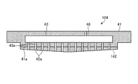
- FIG. 3 is a longitudinal sectional view of Modification 1 of the upper electrode according to the embodiment.
- the upper electrode 104 according to the modified example 1 is different from the upper electrode 4 described with reference to FIG. 2 in that an electrode unit 142 is provided instead of the electrode unit 42. Therefore, the description of the same configuration as the upper electrode 4 described in FIG. 2 is omitted.
- the silicon film thickness is adjusted between the peripheral portion of the electrode portion 142 and the central portion of the electrode portion 142, thereby changing the ratio of the peripheral portion of the electrode portion 142.
- the resistance and the specific resistance at the center of the electrode part 142 are set to different values.
- the specific resistance of the peripheral portion of the electrode portion 142 and the specific resistance of the central portion of the electrode portion 142 are set to different values in the range of 0.01 m ⁇ cm to 100 ⁇ cm.
- the specific resistance of the central portion of the electrode portion 142 is reduced by adjusting the thickness of the silicon at the central portion of the electrode portion 142 to be larger than the thickness of the silicon at the peripheral portion of the electrode portion 142. It is set to a value larger than the specific resistance of the peripheral edge. Thereby, the impedance of the central part of the electrode part 142 with respect to plasma becomes larger than the peripheral part of the electrode part 142.
- the film thickness of silicon at the center portion of the electrode portion 142 is adjusted to be larger than the film thickness of silicon at the peripheral portion of the electrode portion 142, thereby Since the specific resistance is set to a value larger than the specific resistance of the peripheral portion of the electrode portion 142, the impedance of the electrode portion 142 with respect to plasma can be appropriately controlled. As a result, according to the upper electrode 104 of Modification 1, uniform plasma processing can be performed on the entire surface of the wafer W to be processed.
- FIG. 4 is a longitudinal sectional view of Modification 2 of the upper electrode according to the embodiment.
- the upper electrode 204 according to the modified example 2 is different from the upper electrode 4 described with reference to FIG. 2 in that an electrode part 242 is provided instead of the electrode part 42. Therefore, the description of the same configuration as the upper electrode 4 described in FIG. 2 is omitted.
- the silicon film thickness is adjusted between the peripheral portion of the electrode portion 242 and the central portion of the electrode portion 242, thereby changing the ratio of the peripheral portion of the electrode portion 242.
- the resistance and the specific resistance at the center of the electrode portion 242 are set to different values.
- the specific resistance of the peripheral portion of the electrode portion 242 and the specific resistance of the central portion of the electrode portion 242 are set to different values in the range of 0.01 m ⁇ cm to 100 ⁇ cm.
- the specific resistance of the central part of the electrode part 242 is reduced by adjusting the silicon film thickness in the central part of the electrode part 242 to be smaller than the silicon film thickness in the peripheral part of the electrode part 242. It is set to a value smaller than the specific resistance of the peripheral edge. Thereby, the impedance of the center part of the electrode part 242 with respect to plasma becomes smaller than the peripheral part of the electrode part 242.
- the silicon film thickness at the central part of the electrode part 242 is adjusted to be smaller than the silicon film thickness at the peripheral part of the electrode part 242, so that the central part of the electrode part 242 Since the specific resistance is set to a value smaller than the specific resistance of the peripheral portion of the electrode part 242, the impedance of the electrode part 242 with respect to plasma can be appropriately controlled.
- uniform plasma processing can be performed on the entire surface to be processed of the wafer W.
- FIG. 5 is a longitudinal sectional view of Modification 3 of the upper electrode according to the embodiment.
- the upper electrode 304 according to Modification 3 is different from the upper electrode 4 described with reference to FIG. 2 in that a ceramic film portion 344 is formed between the plate-like member 41 and the electrode portion 42. Therefore, the description of the same configuration as the upper electrode 4 described in FIG. 2 is omitted.
- the upper electrode 304 of Modification 3 has a ceramic film part 344 formed in a film shape by spraying ceramic between the plate-like member 41 and the electrode part 42.
- alumina Al 2 O 3
- Y 2 O 3 yttria
- the ceramic film part 344 is formed over the entire surface of the plate-like member 41 and the electrode part 42.
- the ceramic film part 344 is formed with openings that overlap the gas flow holes 43a of the plate-like member 41 and the gas introduction holes 42a of the electrode part 42. Thereby, the processing gas supplied to the gas diffusion chamber 43 is dispersed and supplied into the processing chamber 21 through the gas flow hole 43a, the opening of the ceramic film portion 344 and the gas introduction hole 42a.
- the ceramic film portion 344 can protect the plate-like member 41 from plasma and can appropriately control the impedance of the electrode portion 42 with respect to plasma.
- uniform plasma processing can be performed on the entire processing target surface of the wafer W.
- FIG. 6 is a longitudinal sectional view of Modification 4 of the upper electrode according to the embodiment.
- the upper electrode 404 according to the modification 4 has the same configuration as the upper electrode 304 described with reference to FIG. 5, and the upper electrode 404 described with reference to FIG. 5 is provided with a ceramic film portion 444 instead of the ceramic film portion 344. Different from 304. Therefore, the description of the same configuration as the upper electrode 304 described in FIG. 5 is omitted.
- the upper electrode 404 of Modification 4 has a ceramic film part 444 formed in a film shape by spraying ceramic between the plate-like member 41 and the electrode part 42.
- alumina Al 2 O 3
- Y 2 O 3 yttria
- the ceramic film part 444 is formed at a position corresponding to the central part of the electrode part 42. That is, in the upper electrode 404 of the modified example 4, the ceramic film portion 444 is not formed over the entire surface of the electrode portion 42, but the ceramic film portion 444 is formed only at a position corresponding to the central portion of the electrode portion 42.
- the plate-like member 41 is protected from plasma by the ceramic film portion 444 formed at a position corresponding to the central portion of the electrode portion 42, and the central portion of the electrode portion 42 with respect to plasma.
- the impedance can be increased.
- uniform plasma processing can be performed on the entire processing target surface of the wafer W.
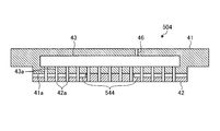
- FIG. 7 is a longitudinal sectional view of Modification 5 of the upper electrode according to the embodiment.
- the upper electrode 504 according to the modification 5 is different from the upper electrode 304 described with reference to FIG. 5 in that a ceramic film part 544 is provided instead of the ceramic film part 344. Therefore, the description of the same configuration as the upper electrode 304 described in FIG. 5 is omitted.
- the upper electrode 504 of the modified example 5 has a ceramic film part 544 formed into a film shape by spraying ceramic between the plate-like member 41 and the electrode part 42.
- alumina Al 2 O 3
- Y 2 O 3 yttria
- the ceramic film part 544 is formed at a position corresponding to the peripheral part of the electrode part 42. That is, in the upper electrode 504 of the modified example 5, the ceramic film part 544 is not formed over the entire surface of the electrode part 42, but is formed only at a position corresponding to the peripheral part of the electrode part 42.
- the plate-like member 41 is protected from plasma by the ceramic film portion 544 formed at a position corresponding to the peripheral portion of the electrode portion 42, and the peripheral portion of the electrode portion 42 with respect to plasma. Can be controlled appropriately.
- uniform plasma processing can be performed on the entire processing target surface of the wafer W.
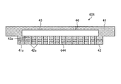
- FIG. 8 is a longitudinal sectional view of Modification 6 of the upper electrode according to the embodiment.
- the upper electrode 604 according to the modification 6 is different from the upper electrode 304 described with reference to FIG. 5 in that a ceramic film part 644 is provided instead of the ceramic film part 344. Therefore, the description of the same configuration as the upper electrode 304 described in FIG. 5 is omitted.
- the upper electrode 604 of Modification 6 has a ceramic film portion 644 formed into a film shape by spraying ceramic between the plate-like member 41 and the electrode portion 42.
- alumina Al 2 O 3
- Y 2 O 3 yttria
- the film thickness of the ceramic film portion 644 is set to a different value at a position corresponding to the peripheral portion of the electrode portion 42 and a position corresponding to the central portion of the electrode portion 42.
- the film thickness of the ceramic film part 644 at the position corresponding to the central part of the electrode part 42 is set to a value larger than the film thickness of the ceramic film part 644 at the position corresponding to the peripheral part of the electrode part 42. The Thereby, the impedance of the center part of the electrode part 42 with respect to plasma becomes larger than the peripheral part of the electrode part 42.
- FIG. 9 is a longitudinal sectional view of Modification 7 of the upper electrode according to the embodiment.
- the upper electrode 704 according to the modified example 7 has the same configuration as the upper electrode 304 described with reference to FIG. 5, and the upper electrode described with reference to FIG. 5 is provided with a ceramic film portion 744 instead of the ceramic film portion 344. Different from 304. Therefore, the description of the same configuration as the upper electrode 304 described in FIG. 5 is omitted.
- the upper electrode 704 of Modification 7 has a ceramic film part 744 formed into a film shape by spraying ceramic between the plate-like member 41 and the electrode part 42.
- alumina Al 2 O 3
- Y 2 O 3 yttria
- the film thickness of the ceramic film part 744 is set to a different value at a position corresponding to the peripheral part of the electrode part 42 and a position corresponding to the central part of the electrode part 42.
- the film thickness of the ceramic film portion 744 at the position corresponding to the central portion of the electrode portion 42 is set to a value smaller than the film thickness of the ceramic film portion 744 at the position corresponding to the peripheral edge portion of the electrode portion 42. The Thereby, the impedance of the central part of the electrode part 42 with respect to plasma becomes smaller than the peripheral part of the electrode part 42.
- the electrode portion 42 is formed in a film shape. It is possible to avoid a situation in which a gap serving as a thermal resistance is generated between the plate-like member 41 and the electrode portion 42. As a result, according to the present embodiment, the uniformity of the temperature of the upper electrode 4 including the plate-like member 41 and the electrode portion 42 can be maintained, so that the entire surface to be processed of the wafer W is uniform. Plasma treatment can be performed.
- Plasma processing apparatus 4 104, 204, 304, 404, 504, 604, 704 Upper electrode 21 Processing chamber (processing vessel) 24 Susceptor (lower electrode) 25 Electrostatic chuck 41 Plate-like member 41a Surfaces 42, 142, 242 Electrode portion 42a Gas introduction hole 43 Gas diffusion chamber 43a Gas flow hole (flow path) 344, 444, 544, 644, 744 Ceramic membrane part
Landscapes
- Chemical & Material Sciences (AREA)
- Engineering & Computer Science (AREA)
- Physics & Mathematics (AREA)
- Plasma & Fusion (AREA)
- Analytical Chemistry (AREA)
- Chemical Kinetics & Catalysis (AREA)
- Materials Engineering (AREA)
- Mechanical Engineering (AREA)
- Metallurgy (AREA)
- Organic Chemistry (AREA)
- Drying Of Semiconductors (AREA)
- Plasma Technology (AREA)
Abstract
Description
4、104、204、304、404、504、604、704 上部電極
21 処理室(処理容器)
24 サセプタ(下部電極)
25 静電チャック
41 板状部材
41a 表面
42、142、242 電極部
42a ガス導入孔
43 ガス拡散室
43a ガス通流孔(流路)
344、444、544、644、744 セラミック膜部
Claims (9)
- プラズマ処理に用いられる処理ガスを通流させる流路が形成された板状部材と、
前記板状部材の前記流路の流出口側の表面に対してシリコンが溶射されることにより膜状に形成された電極部と
を備えたことを特徴とする上部電極。 - 前記電極部の周縁部と前記電極部の中央部とで前記シリコンに添加されるホウ素の濃度が調整されることによって、前記電極部の周縁部の比抵抗と前記電極部の中央部の比抵抗とが異なる値に設定されることを特徴とする請求項1に記載の上部電極。
- 前記電極部の周縁部と前記電極部の中央部とで前記シリコンの膜厚が調整されることによって、前記電極部の周縁部の比抵抗と前記電極部の中央部の比抵抗とが異なる値に設定されることを特徴とする請求項1または2に記載の上部電極。
- 前記電極部の周縁部の比抵抗と前記電極部の中央部の比抵抗とは、0.01mΩcm~100Ωcmの範囲において異なる値に設定されることを特徴とする請求項2に記載の上部電極。
- 前記板状部材と前記電極部との間にセラミックが溶射されることにより膜状に形成されたセラミック膜部をさらに備えたことを特徴とする請求項1または2に記載の上部電極。
- 前記セラミック膜部は、前記電極部の中央部に対応する位置に形成されることを特徴とする請求項5に記載の上部電極。
- 前記セラミック膜部は、前記電極部の周縁部に対応する位置に形成されることを特徴とする請求項5に記載の上部電極。
- 前記セラミック膜部の膜厚は、前記電極部の周縁部に対応する位置と前記電極部の中央部に対応する位置とで異なる値に設定されることを特徴とする請求項5に記載の上部電極。
- プラズマ処理空間を画成する処理容器と、
前記処理容器内に設けられ、被処理基板が載置される下部電極と、
前記プラズマ処理空間を介して前記下部電極と対向して配置された上部電極と
を備えたプラズマ処理装置であって、
前記上部電極は、
プラズマ処理に用いられる処理ガスを通流させる流路が形成された板状部材と、
前記板状部材の前記流路の流出口側の表面に対してシリコンが溶射されることにより膜状に形成された電極部と
を備えたことを特徴とするプラズマ処理装置。
Priority Applications (4)
| Application Number | Priority Date | Filing Date | Title |
|---|---|---|---|
| US14/415,258 US20150179405A1 (en) | 2012-07-17 | 2013-07-02 | Upper electrode and plasma processing apparatus |
| KR1020157001213A KR102025457B1 (ko) | 2012-07-17 | 2013-07-02 | 상부 전극, 및 플라즈마 처리 장치 |
| US16/296,827 US11515125B2 (en) | 2012-07-17 | 2019-03-08 | Upper electrode and plasma processing apparatus |
| US17/983,128 US20230061699A1 (en) | 2012-07-17 | 2022-11-08 | Upper electrode and plasma processing apparatus |
Applications Claiming Priority (4)
| Application Number | Priority Date | Filing Date | Title |
|---|---|---|---|
| JP2012158841A JP6068849B2 (ja) | 2012-07-17 | 2012-07-17 | 上部電極、及びプラズマ処理装置 |
| JP2012-158841 | 2012-07-17 | ||
| US201261674509P | 2012-07-23 | 2012-07-23 | |
| US61/674,509 | 2012-07-23 |
Related Child Applications (2)
| Application Number | Title | Priority Date | Filing Date |
|---|---|---|---|
| US14/415,258 A-371-Of-International US20150179405A1 (en) | 2012-07-17 | 2013-07-02 | Upper electrode and plasma processing apparatus |
| US16/296,827 Division US11515125B2 (en) | 2012-07-17 | 2019-03-08 | Upper electrode and plasma processing apparatus |
Publications (1)
| Publication Number | Publication Date |
|---|---|
| WO2014013864A1 true WO2014013864A1 (ja) | 2014-01-23 |
Family
ID=49948696
Family Applications (1)
| Application Number | Title | Priority Date | Filing Date |
|---|---|---|---|
| PCT/JP2013/068167 Ceased WO2014013864A1 (ja) | 2012-07-17 | 2013-07-02 | 上部電極、及びプラズマ処理装置 |
Country Status (5)
| Country | Link |
|---|---|
| US (3) | US20150179405A1 (ja) |
| JP (1) | JP6068849B2 (ja) |
| KR (1) | KR102025457B1 (ja) |
| TW (1) | TWI585849B (ja) |
| WO (1) | WO2014013864A1 (ja) |
Families Citing this family (7)
| Publication number | Priority date | Publication date | Assignee | Title |
|---|---|---|---|---|
| JP6541355B2 (ja) * | 2015-01-09 | 2019-07-10 | 東京エレクトロン株式会社 | 冷却構造及び平行平板エッチング装置 |
| KR20170073757A (ko) * | 2015-12-18 | 2017-06-29 | 삼성전자주식회사 | 플라즈마 처리 장치용 상부 전극 및 이를 포함하는 플라즈마 처리 장치 |
| US10964514B2 (en) * | 2017-10-17 | 2021-03-30 | Lam Research Corporation | Electrode for plasma processing chamber |
| DE102018126617A1 (de) * | 2018-10-25 | 2020-04-30 | Aixtron Se | Schirmplatte für einen CVD-Reaktor |
| JP7345382B2 (ja) * | 2018-12-28 | 2023-09-15 | 東京エレクトロン株式会社 | プラズマ処理装置及び制御方法 |
| JP7172717B2 (ja) * | 2019-02-25 | 2022-11-16 | 三菱マテリアル株式会社 | プラズマ処理装置用電極板 |
| US12125680B2 (en) * | 2021-10-27 | 2024-10-22 | Applied Materials, Inc. | Ion extraction assembly having variable electrode thickness for beam uniformity control |
Citations (3)
| Publication number | Priority date | Publication date | Assignee | Title |
|---|---|---|---|---|
| JP2011155235A (ja) * | 2009-03-06 | 2011-08-11 | Tokyo Electron Ltd | プラズマ処理装置及びプラズマ処理装置用の電極 |
| JP2012084848A (ja) * | 2010-09-16 | 2012-04-26 | Tokyo Electron Ltd | プラズマ処理装置及びプラズマ処理方法 |
| JP2012109377A (ja) * | 2010-11-17 | 2012-06-07 | Tokyo Electron Ltd | 電極構造及びプラズマ処理装置 |
Family Cites Families (22)
| Publication number | Priority date | Publication date | Assignee | Title |
|---|---|---|---|---|
| JP3308091B2 (ja) * | 1994-02-03 | 2002-07-29 | 東京エレクトロン株式会社 | 表面処理方法およびプラズマ処理装置 |
| US5569356A (en) * | 1995-05-19 | 1996-10-29 | Lam Research Corporation | Electrode clamping assembly and method for assembly and use thereof |
| TW335517B (en) * | 1996-03-01 | 1998-07-01 | Hitachi Ltd | Apparatus and method for processing plasma |
| US6121540A (en) * | 1998-06-30 | 2000-09-19 | Kabushiki Kaisha Toshiba | Composite material substrate for solar cells, and solar cell |
| US20050061445A1 (en) * | 1999-05-06 | 2005-03-24 | Tokyo Electron Limited | Plasma processing apparatus |
| US6228438B1 (en) * | 1999-08-10 | 2001-05-08 | Unakis Balzers Aktiengesellschaft | Plasma reactor for the treatment of large size substrates |
| US6894245B2 (en) * | 2000-03-17 | 2005-05-17 | Applied Materials, Inc. | Merie plasma reactor with overhead RF electrode tuned to the plasma with arcing suppression |
| JP4454781B2 (ja) * | 2000-04-18 | 2010-04-21 | 東京エレクトロン株式会社 | プラズマ処理装置 |
| TW518690B (en) | 2000-09-14 | 2003-01-21 | Tokyo Electron Ltd | Plasma processing apparatus and its electrode plate, its electrode supporting body and its shield ring |
| JP4047616B2 (ja) * | 2002-04-03 | 2008-02-13 | 東京エレクトロン株式会社 | プラズマ処理装置及びプラズマ処理方法 |
| US20060019103A1 (en) * | 2003-01-28 | 2006-01-26 | Masanori Abe | Corrosion-resistant member and method forproducing same |
| WO2004073850A1 (en) * | 2003-02-14 | 2004-09-02 | Tokyo Electron Limited | Gas feeding apparatus |
| JP4349952B2 (ja) * | 2004-03-24 | 2009-10-21 | 京セラ株式会社 | ウェハ支持部材とその製造方法 |
| JP5040119B2 (ja) * | 2006-02-22 | 2012-10-03 | 東京エレクトロン株式会社 | 耐環境部材、半導体製造装置及び耐環境部材の製造方法 |
| US7895970B2 (en) * | 2005-09-29 | 2011-03-01 | Tokyo Electron Limited | Structure for plasma processing chamber, plasma processing chamber, plasma processing apparatus, and plasma processing chamber component |
| CN101847574B (zh) * | 2006-01-31 | 2012-11-07 | 东京毅力科创株式会社 | 基板处理装置和暴露于等离子体的部件 |
| JP2007250569A (ja) * | 2006-03-13 | 2007-09-27 | Tokyo Electron Ltd | プラズマ処理装置およびプラズマに曝される部材 |
| JP2007243020A (ja) * | 2006-03-10 | 2007-09-20 | Hitachi High-Technologies Corp | プラズマ処理装置 |
| JP4935149B2 (ja) | 2006-03-30 | 2012-05-23 | 東京エレクトロン株式会社 | プラズマ処理用の電極板及びプラズマ処理装置 |
| JP5361457B2 (ja) * | 2009-03-06 | 2013-12-04 | 東京エレクトロン株式会社 | プラズマ処理装置及びプラズマ処理装置用の電極 |
| JP5359642B2 (ja) * | 2009-07-22 | 2013-12-04 | 東京エレクトロン株式会社 | 成膜方法 |
| SG192967A1 (en) * | 2011-03-04 | 2013-09-30 | Novellus Systems Inc | Hybrid ceramic showerhead |
-
2012
- 2012-07-17 JP JP2012158841A patent/JP6068849B2/ja active Active
-
2013
- 2013-07-02 WO PCT/JP2013/068167 patent/WO2014013864A1/ja not_active Ceased
- 2013-07-02 US US14/415,258 patent/US20150179405A1/en not_active Abandoned
- 2013-07-02 KR KR1020157001213A patent/KR102025457B1/ko active Active
- 2013-07-16 TW TW102125401A patent/TWI585849B/zh active
-
2019
- 2019-03-08 US US16/296,827 patent/US11515125B2/en active Active
-
2022
- 2022-11-08 US US17/983,128 patent/US20230061699A1/en active Pending
Patent Citations (3)
| Publication number | Priority date | Publication date | Assignee | Title |
|---|---|---|---|---|
| JP2011155235A (ja) * | 2009-03-06 | 2011-08-11 | Tokyo Electron Ltd | プラズマ処理装置及びプラズマ処理装置用の電極 |
| JP2012084848A (ja) * | 2010-09-16 | 2012-04-26 | Tokyo Electron Ltd | プラズマ処理装置及びプラズマ処理方法 |
| JP2012109377A (ja) * | 2010-11-17 | 2012-06-07 | Tokyo Electron Ltd | 電極構造及びプラズマ処理装置 |
Also Published As
| Publication number | Publication date |
|---|---|
| US20150179405A1 (en) | 2015-06-25 |
| US20190272977A1 (en) | 2019-09-05 |
| US11515125B2 (en) | 2022-11-29 |
| US20230061699A1 (en) | 2023-03-02 |
| KR102025457B1 (ko) | 2019-09-25 |
| JP2014022517A (ja) | 2014-02-03 |
| TWI585849B (zh) | 2017-06-01 |
| KR20150036100A (ko) | 2015-04-07 |
| TW201417171A (zh) | 2014-05-01 |
| JP6068849B2 (ja) | 2017-01-25 |
Similar Documents
| Publication | Publication Date | Title |
|---|---|---|
| US11380526B2 (en) | Stage and plasma processing apparatus | |
| US20230061699A1 (en) | Upper electrode and plasma processing apparatus | |
| TWI494995B (zh) | Buffer plate and substrate processing device | |
| TWI480949B (zh) | Substrate handling device and sprinkler | |
| TWI445124B (zh) | A substrate stage, a substrate processing apparatus, and a substrate to be processed | |
| JP6453240B2 (ja) | 取り外し可能なガス分配プレートを有するシャワーヘッド | |
| CN102569130B (zh) | 基板处理装置及基板处理方法 | |
| JP5893516B2 (ja) | 被処理体の処理装置及び被処理体の載置台 | |
| US20130014895A1 (en) | Substrate processing apparatus | |
| JP2013533640A (ja) | 処理チャンバ内のガスの流れを制御するための装置 | |
| US11978614B2 (en) | Substrate processing apparatus | |
| KR20200103556A (ko) | 거치대 및 기판 처리 장치 | |
| US8529730B2 (en) | Plasma processing apparatus | |
| TW201737389A (zh) | 基板處理裝置 | |
| JP6932070B2 (ja) | フォーカスリング及び半導体製造装置 | |
| TW202204677A (zh) | 用於高頻處理的蓋堆疊 | |
| WO2023058480A1 (ja) | 上部電極構造及びプラズマ処理装置 | |
| CN110246741B (zh) | 基板载置构造体和等离子体处理装置 | |
| US11664198B2 (en) | Plasma processing apparatus | |
| JP2015128110A (ja) | 基板処理装置、シャッタ機構およびプラズマ処理装置 | |
| JP7113733B2 (ja) | 基板処理装置用構造物及び基板処理装置 | |
| CN113555269A (zh) | 配管系统和处理装置 | |
| JP2014075281A (ja) | プラズマ処理装置及び温度制御方法 | |
| KR101171988B1 (ko) | 플라즈마 처리장치 |
Legal Events
| Date | Code | Title | Description |
|---|---|---|---|
| 121 | Ep: the epo has been informed by wipo that ep was designated in this application |
Ref document number: 13819207 Country of ref document: EP Kind code of ref document: A1 |
|
| ENP | Entry into the national phase |
Ref document number: 20157001213 Country of ref document: KR Kind code of ref document: A |
|
| WWE | Wipo information: entry into national phase |
Ref document number: 14415258 Country of ref document: US |
|
| NENP | Non-entry into the national phase |
Ref country code: DE |
|
| 122 | Ep: pct application non-entry in european phase |
Ref document number: 13819207 Country of ref document: EP Kind code of ref document: A1 |