WO2014010459A1 - Circuit de commande et procédé de commande - Google Patents
Circuit de commande et procédé de commande Download PDFInfo
- Publication number
- WO2014010459A1 WO2014010459A1 PCT/JP2013/068082 JP2013068082W WO2014010459A1 WO 2014010459 A1 WO2014010459 A1 WO 2014010459A1 JP 2013068082 W JP2013068082 W JP 2013068082W WO 2014010459 A1 WO2014010459 A1 WO 2014010459A1
- Authority
- WO
- WIPO (PCT)
- Prior art keywords
- switch
- fet
- gate
- turned
- voltage
- Prior art date
Links
- 238000000034 method Methods 0.000 title claims abstract description 42
- 239000003990 capacitor Substances 0.000 claims description 47
- 238000001514 detection method Methods 0.000 claims description 22
- 230000005669 field effect Effects 0.000 claims description 7
- 230000008929 regeneration Effects 0.000 abstract description 20
- 238000011069 regeneration method Methods 0.000 abstract description 20
- 238000010586 diagram Methods 0.000 description 40
- 230000008569 process Effects 0.000 description 26
- 230000005540 biological transmission Effects 0.000 description 19
- 238000005516 engineering process Methods 0.000 description 12
- 238000004088 simulation Methods 0.000 description 11
- 230000007423 decrease Effects 0.000 description 6
- 230000007246 mechanism Effects 0.000 description 5
- 230000008602 contraction Effects 0.000 description 4
- 230000005674 electromagnetic induction Effects 0.000 description 4
- 230000004907 flux Effects 0.000 description 4
- 238000004891 communication Methods 0.000 description 3
- 238000006073 displacement reaction Methods 0.000 description 3
- 230000006870 function Effects 0.000 description 3
- 239000004065 semiconductor Substances 0.000 description 3
- 230000000295 complement effect Effects 0.000 description 2
- 230000033001 locomotion Effects 0.000 description 2
- 238000009774 resonance method Methods 0.000 description 2
- 238000009825 accumulation Methods 0.000 description 1
- 230000008859 change Effects 0.000 description 1
- 230000003247 decreasing effect Effects 0.000 description 1
- 230000003111 delayed effect Effects 0.000 description 1
- 230000005484 gravity Effects 0.000 description 1
- 230000001771 impaired effect Effects 0.000 description 1
- 239000004973 liquid crystal related substance Substances 0.000 description 1
- 229910044991 metal oxide Inorganic materials 0.000 description 1
- 150000004706 metal oxides Chemical class 0.000 description 1
- 238000012986 modification Methods 0.000 description 1
- 230000004048 modification Effects 0.000 description 1
- 230000003287 optical effect Effects 0.000 description 1
- 230000001172 regenerating effect Effects 0.000 description 1
- 230000004044 response Effects 0.000 description 1
- 230000002441 reversible effect Effects 0.000 description 1
Images


Classifications
-
- H—ELECTRICITY
- H02—GENERATION; CONVERSION OR DISTRIBUTION OF ELECTRIC POWER
- H02J—CIRCUIT ARRANGEMENTS OR SYSTEMS FOR SUPPLYING OR DISTRIBUTING ELECTRIC POWER; SYSTEMS FOR STORING ELECTRIC ENERGY
- H02J7/00—Circuit arrangements for charging or depolarising batteries or for supplying loads from batteries
-
- H—ELECTRICITY
- H03—ELECTRONIC CIRCUITRY
- H03K—PULSE TECHNIQUE
- H03K17/00—Electronic switching or gating, i.e. not by contact-making and –breaking
- H03K17/51—Electronic switching or gating, i.e. not by contact-making and –breaking characterised by the components used
- H03K17/56—Electronic switching or gating, i.e. not by contact-making and –breaking characterised by the components used by the use, as active elements, of semiconductor devices
- H03K17/687—Electronic switching or gating, i.e. not by contact-making and –breaking characterised by the components used by the use, as active elements, of semiconductor devices the devices being field-effect transistors
-
- H02J5/005—
-
- H—ELECTRICITY
- H02—GENERATION; CONVERSION OR DISTRIBUTION OF ELECTRIC POWER
- H02J—CIRCUIT ARRANGEMENTS OR SYSTEMS FOR SUPPLYING OR DISTRIBUTING ELECTRIC POWER; SYSTEMS FOR STORING ELECTRIC ENERGY
- H02J50/00—Circuit arrangements or systems for wireless supply or distribution of electric power
- H02J50/10—Circuit arrangements or systems for wireless supply or distribution of electric power using inductive coupling
- H02J50/12—Circuit arrangements or systems for wireless supply or distribution of electric power using inductive coupling of the resonant type
-
- H—ELECTRICITY
- H02—GENERATION; CONVERSION OR DISTRIBUTION OF ELECTRIC POWER
- H02J—CIRCUIT ARRANGEMENTS OR SYSTEMS FOR SUPPLYING OR DISTRIBUTING ELECTRIC POWER; SYSTEMS FOR STORING ELECTRIC ENERGY
- H02J50/00—Circuit arrangements or systems for wireless supply or distribution of electric power
- H02J50/40—Circuit arrangements or systems for wireless supply or distribution of electric power using two or more transmitting or receiving devices
-
- H02J7/025—
-
- H—ELECTRICITY
- H03—ELECTRONIC CIRCUITRY
- H03K—PULSE TECHNIQUE
- H03K17/00—Electronic switching or gating, i.e. not by contact-making and –breaking
- H03K17/04—Modifications for accelerating switching
- H03K17/041—Modifications for accelerating switching without feedback from the output circuit to the control circuit
- H03K17/0412—Modifications for accelerating switching without feedback from the output circuit to the control circuit by measures taken in the control circuit
- H03K17/04123—Modifications for accelerating switching without feedback from the output circuit to the control circuit by measures taken in the control circuit in field-effect transistor switches
-
- H—ELECTRICITY
- H02—GENERATION; CONVERSION OR DISTRIBUTION OF ELECTRIC POWER
- H02J—CIRCUIT ARRANGEMENTS OR SYSTEMS FOR SUPPLYING OR DISTRIBUTING ELECTRIC POWER; SYSTEMS FOR STORING ELECTRIC ENERGY
- H02J7/00—Circuit arrangements for charging or depolarising batteries or for supplying loads from batteries
- H02J7/007—Regulation of charging or discharging current or voltage
- H02J7/00712—Regulation of charging or discharging current or voltage the cycle being controlled or terminated in response to electric parameters
-
- H—ELECTRICITY
- H03—ELECTRONIC CIRCUITRY
- H03K—PULSE TECHNIQUE
- H03K2217/00—Indexing scheme related to electronic switching or gating, i.e. not by contact-making or -breaking covered by H03K17/00
- H03K2217/009—Resonant driver circuits
Definitions
- the present technology relates to a drive circuit and a drive method, and more particularly, to a drive circuit and a drive method that can reduce a loss when switching a FET (Field Effect Transistor) with a simple circuit.
- FET Field Effect Transistor
- Wireless power supply requires a high-frequency power source that can output AC signals (voltage, current) such as a sine wave with a certain amount of power.
- a high-frequency power supply generally has a simple circuit configuration and high efficiency, and an inverter that generates a rectangular wave by switching operation. Used.
- a power MOS FET Metal Oxide Semiconductor Semiconductor FET
- a switching element that performs a switching operation.
- FIG. 1 is a diagram showing a configuration of an example of a portion that performs switching of a conventional inverter.
- the source of the FET 1 is grounded (connected to the ground), and the drain is connected to a terminal or a line (not shown) whose connection to the ground should be switched (ON / OFF).
- a pulse (gate pulse) output from the pulse output unit 2 is supplied to the gate of the FET 1, and the FET 1 (gate) is driven by a pulse output from the pulse output unit 2.
- the FET 1 is an nMOS (negative channel MOS) FET, which is turned on when the H (High) level is applied to the gate and is applied when the L (Low) level is applied (the H level is not applied). And) turn off.
- nMOS negative channel MOS
- the FET 1 performs a switching operation that turns on when the pulse output from the pulse output unit 2 is at the H (High) level and turns off when the pulse is at the L (Low) level.
- the FET 1 is required to be a power MOS FET having a small resistance (on-resistance) between the drain and the source in order to increase the efficiency of the inverter.
- FET 1 can be obtained from the pulse output unit 2 (driver) that outputs a pulse for driving FET 1 having such a large input capacitance C iss. A heavy capacitive load.
- Patent Document 1 proposes a gate drive circuit for a power MOS FET that reduces energy loss by storing current by flowing current through the coil and regenerating the energy.
- the present technology has been made in view of such a situation, and makes it possible to reduce a loss when switching an FET with a simple circuit.
- a driving circuit includes a coil that forms a resonance circuit together with an input capacitance of a gate of an FET (Field Effect Transistor), a first switch that turns on or off a current flowing through the coil, and a charge in the resonance circuit.
- the FET drive circuit includes a DC power source connected to the gate of the FET and a second switch that turns on or off the connection between the DC power source and the gate of the FET.
- the current flowing through the coil constituting the resonance circuit together with the input capacitance of the gate of the FET is turned on or off.
- a DC power supply for replenishing the resonance circuit with a charge is connected to the gate of the FET, and the connection is turned on or off.
- a driving method includes a coil that forms a resonance circuit together with an input capacitance of a gate of an FET (Field Effect Transistor), a first switch that turns on or off a current flowing through the coil, and a charge that is applied to the resonance circuit.
- the first switch of the FET drive circuit comprising: a DC power source connected to the gate of the FET, and a second switch for turning on or off the connection between the DC power source and the gate of the FET.
- Drive that is temporarily turned on in a cycle corresponding to the cycle for switching the FET, and the second switch is periodically turned on for a predetermined period of time during which the first switch is off. Is the method.
- the first switch for turning on or off the current flowing in the coil constituting the resonance circuit together with the input capacitance of the gate of the FET is temporarily turned on in a cycle corresponding to the cycle for switching the FET.
- the second switch for turning on or off the connection between the DC power source for replenishing electric charge to the resonance circuit and the gate of the FET is only for a predetermined period of the period in which the first switch is off. , Periodically turned on.
- the drive circuit may be an independent device or may be an internal block constituting one device.
- the loss when switching the FET can be reduced with a simple circuit.
- FIG. 2 is a block diagram illustrating a configuration example of a power transmission device 11.
- FIG. 3 is a circuit diagram illustrating a first configuration example of a gate drive circuit 31.
- FIG. It is a wave form diagram which shows the control signal C1 which the control part outputs, and the control signal C2 which the control part 52 outputs.
- a control signal C2 which is a waveform diagram illustrating the current i 2 flowing through the switch 51 is controlled in accordance with the control signal C2.
- Control signal C1 the current i 1 flows through the switch 41 is controlled in accordance with the control signal C1, and is a waveform diagram showing the gate voltage. It is a diagram illustrating the relationship between the current i 1 and the gate voltage. It is a figure explaining a response
- FIG. 5 is a waveform diagram showing a control signal C2, a current i 2 that flows when a switch 51 is turned on / off, a control signal C1, a current i 1 that flows when a switch 41 is turned on / off, and a gate voltage. It is a circuit diagram which shows the circuit used for simulation. 6 is a circuit diagram illustrating a third configuration example of the gate drive circuit 31.
- FIG. FIG. 5 is a waveform diagram showing a control signal C2, a current i 2 that flows when a switch 51 is turned on / off, a control signal C1, a current i 1 that flows when a switch 41 is turned on / off, and a gate voltage.
- 4 is a flowchart illustrating control of a switch 41 by a control unit 72.
- FIG. 6 is a circuit diagram illustrating a fourth configuration example of the gate drive circuit 31.
- FIG. 7 is a circuit diagram showing a fifth configuration example of the gate drive circuit 31.
- FIG. FIG. 5 is a waveform diagram showing a control signal C2, a current i 2 that flows when a switch 51 is turned on / off, a control signal C1, a current i 1 that flows when a switch 41 is turned on / off, and a gate voltage.
- 4 is a flowchart illustrating control of a switch 41 by a control unit 82.
- FIG. 18 is a block diagram illustrating a configuration example of an embodiment of a computer to which the present technology is applied.
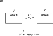
- FIG. 2 is a block diagram illustrating a configuration example of an embodiment of a wireless power feeding system to which the present technology is applied.
- the wireless power feeding system includes a power transmitting device 11 and a power receiving device 12, and performs wireless power feeding by, for example, an electromagnetic induction method using a magnetic field or a magnetic field resonance method.
- the power transmission device 11 has a power transmission coil that is a coil for transmitting electric power using a magnetic field, and transmits electric power.
- the power receiving device 12 has a power receiving coil that is a coil for receiving power using a magnetic field, and receives power transmitted from the power transmitting device 11 when placed near the power transmitting device 11. .
- a set of, for example, a cradle as the power transmission apparatus 11 and a portable terminal such as a mobile phone as the power reception apparatus 12, or the power transmission apparatus 11 for example, a charging stand and a set of, for example, an electric vehicle as the power receiving device 12, a set of, for example, a TV rack and a TV (television receiver) as the power receiving device 12, as the power transmitting device 11.
- a charging stand and a set of, for example, an electric vehicle as the power receiving device 12 a set of, for example, a TV rack and a TV (television receiver) as the power receiving device 12, as the power transmitting device 11.
- FIG. 2 only one power receiving device 12 is illustrated as a power receiving device that receives power from one power transmitting device 11 by wireless power feeding. However, there are a plurality of power receiving devices that receive power by wireless power feeding. There may be.
- a wireless power feeding system having a plurality of power receiving devices, for example, by placing a plurality of portable terminals as a plurality of power receiving devices, for example, on a tray (charging tray) as the power transmitting device 11, the plurality of portable devices. You can charge your device at the same time.
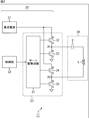
- FIG. 3 is a block diagram illustrating a configuration example of the power transmission device 11 of FIG.
- the power transmission device 11 includes a high-frequency power source 20 and a resonance circuit 24, and functions as a power source that performs wireless power feeding.
- the high-frequency power source 20 includes a DC power source 21, a control unit 22, and a driver circuit 23, and functions as a power source that outputs a rectangular wave voltage and current as AC by switching.
- the DC power supply 21 supplies a predetermined DC voltage (current) to the driver circuit 23.
- the control unit 22 controls the driver circuit 23 (the gate drive circuit 31 thereof) and each block constituting the power transmission device 11.
- the driver circuit (inverter) 23 uses a DC voltage from the DC power supply 21 to drive the resonance circuit 24 and generate a magnetic flux in the power transmission coil L that constitutes the resonance circuit 24, thereby causing electromagnetic induction or magnetic resonance. In this method, power is transmitted.
- the resonance circuit 24 is a series resonance circuit including a power transmission coil L and a capacitor C, and is driven by the driver circuit 23.
- a magnetic flux magnetic field
- wireless power feeding is performed by which the power is transmitted to the power receiving device 12 by an electromagnetic induction method or a magnetic field resonance method. .
- the driver circuit 23 forms a full-bridge inverter, and includes a gate drive circuit 31 and NMOS FETs 32, 33, 34, and 35.
- the gate drive circuit 31 turns on or off (turns on or off) each of the FETs 32 to 35 by applying a predetermined voltage to the gates of the FETs 32 to 35 under the control of the control unit 22.
- FETs 32 to 35 are power MOS FETs and are turned on or off (turned on and off) according to the driving of the gate drive circuit 31.
- the drain of the FET 32 is connected to the DC power source 21, and accordingly, a predetermined DC voltage output from the DC power source 21 is applied to the drain of the FET 32.
- the source of the FET 32 is connected to the drain of the FET 33, and the source of the FET 33 is grounded (connected to the ground (GND)).
- FETs 34 and 35 are connected in the same manner as FETs 32 and 33.
- the drain of the FET 34 is connected to the DC power supply 21, and the source of the FET 34 is connected to the drain of the FET 35.
- the source of the FET 35 is grounded.
- one end of the resonance circuit 24 is connected to a connection point P1 between the source of the FET 32 and the drain of the FET 33, and the other end of the resonance circuit 24 is connected to a connection point P2 between the source of the FET 34 and the drain of the FET 35. ing.
- one end of the power transmission coil L and the capacitor C is connected in the resonance circuit 24.
- the other end of the capacitor C is connected to a connection point P1 between the source of the FET 32 and the drain of the FET 33, and the other end of the power transmission coil L is connected to a connection point P2 between the source of the FET 34 and the drain of the FET 35. .
- the gate driving circuit 31 applies a predetermined voltage to the gates of the FETs 32 to 35 at a predetermined timing in accordance with the control of the control unit 22, so that the FETs 32 to 35 are respectively connected. Control to turn on or off.
- the FETs 32 and 33 are turned on and off in a complementary manner and periodically, respectively.
- the FET 32 is alternately turned on and off periodically.
- the set of FETs 34 and 35 is turned on and off in a complementary manner to the set of FETs 32 and 33 and periodically.
- connection point P1 between the source of the FET 32 and the drain of the FET 33 becomes a predetermined direct current voltage output from the DC power source 21, for example, H (High) level, and the source of the FET 34 and the drain of the FET 35 are connected.
- the connection point P2 is a ground level, for example, an L (Low) level.
- a current flows in a direction from the connection point P1 to the connection point P2 via the capacitor C and the power transmission coil L.
- connection point P2 between the source of the FET 34 and the drain of the FET 35 becomes an H level that is a predetermined DC voltage output from the DC power supply 21, and the connection point P1 between the source of the FET 32 and the drain of the FET 33 is the ground. It becomes the L level which is the level of.
- a current flows in a direction from the connection point P2 toward the connection point P1 via the power transmission coil L and the capacitor C.
- the resonance circuit 24 is applied with an AC voltage (rectangular wave voltage) with a period in which the FETs 32 to 35 are turned on (or off), and an AC with a similar period is applied according to the application of the AC voltage. Current flows.
- AC voltage rectangular wave voltage
- the period in which the FETs 32 to 35 are turned on (or off) is the resonance period 2 ⁇ (LC) of the resonance circuit 24 composed of the power transmission coil L and the capacitor C, that is, the resonance frequency 1 / ( It is set to the reciprocal of 2 ⁇ (LC)).
- a full bridge inverter is used as the driver circuit 23.
- the driver circuit 23 for example, a circuit that performs switching (ON / OFF) of an FET such as a half bridge inverter is used. be able to.
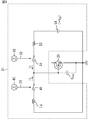
- FIG. 4 is a circuit diagram showing a first configuration example of the gate drive circuit 31 of FIG.
- FIG. 4 illustrates a configuration example of a portion for driving, for example, the FET 33 in the gate drive circuit 31 of FIG.
- the parts that drive the FETs 32, 34, and 35 other than the FET 33 are configured in the same manner.
- the gate drive circuit 31 has a power regeneration mechanism that regenerates the power used to drive the FET in order to drive the power MOS FET (gate) of the capacitive load with high efficiency.
- the gate drive circuit 31 includes a coil (regeneration coil) L g , a switch (regeneration switch) 41, a control unit 42, a switch (replenishment switch) 51, a control unit 52, a resistor (current limiting resistor). ) 53 and a DC power supply 54.
- the coil L g constitutes the gate input capacitance (capacitor) with C iss of FET33 the (series) resonant circuit.
- Switch 41 (first switch), one end of the coil L g, is provided between the gate of the FET 33. Switch 41, the control of the control unit 42, i.e., in accordance with the control signal C1 supplied from the control unit 42, on or off, thereby turning on or off the current i 1 flowing through the coil L g.
- the current i 1 flowing through the coil L g is a coil L g, the direction of flow to the gate of the FET 33, as well as the positive direction, the reverse direction, a negative direction.
- the control unit 42 controls the switch 41 (on / off) by supplying a control signal (regeneration switch control signal) C1 to the switch 41.
- the switch 51 (second switch) is turned on or off in accordance with control from the control unit 52, that is, a control signal (supplementary switch control signal) C2 supplied from the control unit 52, whereby the DC power supply 54 and the FET 33 are turned on. Turn on or off the connection to the gate.
- the plus terminal of the DC power supply 54 is connected to the gate of the FET 33 via the resistor 53 and the switch 51, and the minus terminal of the DC power supply 54 is connected to the source of the FET 33.
- the controller 52 controls the switch 51 (on / off) by supplying the control signal C2 to the switch 51.
- the resistor 53 is a resistor for limiting the current i 2 flowing from the DC power source 54 when the switch 51 is turned on.
- One end of the resistor 53 is connected to the plus terminal of the DC power source 54, and the other end of the resistor 53 Is connected to the gate of the FET 33 via the switch 51.
- the current flowing from the DC power supply 54 (current flowing through the resistor 53) i 2 is set to the forward direction from the plus terminal of the DC power supply 54 to the gate of the FET 33 and vice versa.
- the direction is the negative direction.
- the DC power supply 54 is a power supply that outputs a predetermined DC voltage + V DD (> 0).
- the positive terminal of the DC power supply 54 is connected to the gate of the FET 33 via the resistor 53 and the switch 51, and the negative terminal of the DC power supply 54 is connected to the source of the FET 33. Therefore, when the switch 51 is turned on, the (direct current) voltage + V DD of the direct current power source 54 is applied to the gate of the FET 33.
- the voltage + V DD of the DC power supply 54 is a voltage sufficient to drive the FET 33 (a voltage greater than the voltage v gs between the gate and the source when the FET 33 is turned on). .
- the input capacitance C iss of the gate of the FET 33 is equivalently present in parallel between the gate and the source of the FET 33.
- the input capacitance C iss of the gate of the FET 33, the coil L g , the switch 41, and the control unit 42 regenerate the power used to drive the FET 33. Is configured.
- the gate of the input capacitance C iss of FET 33, the charge accumulation, the voltage of the gate (the voltage of the gate as seen from the source), the H level ing.
- the voltage of the gate of FET33 at this time i.e., the input capacitance C iss, referenced to the terminal connected to the source, the voltage of the terminal connected to the gate, for example, the voltage of the DC power supply 54 + Suppose that it is V DD .
- the switch 41 is turned on at the timing when the FET 33 should be turned off (switched) in accordance with the control of the control unit 42.
- switch 41 By switch 41 is turned on, the charge accumulated in the input capacitance C iss, the switches 41 and discharges through the coil L g, the coil L g, the current i corresponding to the electric charge discharged 1 flows in the negative direction.
- the FET 33 When the charge accumulated in the input capacitance C iss is discharged to some extent and the gate voltage falls below the voltage + V DD to a predetermined value (the gate voltage at which the FET 33 is turned on), the FET 33 is turned off.
- the coil L g when a current i 1 continues to flow, the input capacitance C iss, charges are accumulated, a reference voltage (input capacitance C iss gate, a terminal connected to the source of FET 33, When the polarity of the voltage of the terminal connected to the gate is reversed, that is, when the voltage of the gate of the FET 33 becomes the voltage ⁇ V DD , the current i 1 flowing through the coil L g becomes zero.
- Switch 41 under the control of the control unit 42, at the timing when the current i 1 flowing through the coil L g is 0, it turned off. Thereby, the voltage of the gate of the FET 33 is maintained at the voltage ⁇ V DD .
- the switch 41 is turned on at the timing when the FET 33 should be turned on (switched) in accordance with the control of the control unit 42.
- the coil L g when a current i 1 flows, electric energy corresponding to the current i 1 is accumulated in the coil L g.
- the FET 33 When the charge accumulated in the input capacitance C iss is discharged to some extent and the gate voltage rises from the voltage ⁇ V DD to a predetermined value or more, the FET 33 is turned on.
- Switch 41 under the control of the control unit 42, at the timing when the current i 1 flowing through the coil L g is 0, it turned off. As a result, the voltage of the gate of the FET 33 is maintained at the voltage + V DD .
- the switch 41 is turned on at the timing when the FET 33 should be turned off in accordance with the control of the control unit 42, and the same operation is repeated thereafter.
- power regeneration mechanism as the input capacitance C iss, coil L g, switches 41 and, the control unit 42, the electric energy (electric charge) accumulated in the input capacitance C iss, with its input capacitance C iss accumulated in the coil L g which constitutes a resonance circuit, the electric energy stored in the coil L g, by repeating to accumulate in the input capacitance C iss, it regenerates electric power used for driving the FET 33, the power Is again used to drive the FET 33.
- the switch 51 is temporarily turned on, for example, periodically (from off to on) according to the control of the control unit 52.
- the DC power supply 54 can be referred to as a power supply for replenishing electric charges (power), and the current i 2 flowing from the DC power supply 54 can be referred to as a replenishing current for replenishing charges (electric power).
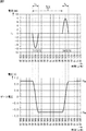
- FIG. 5 is a waveform diagram showing the control signal C1 output from the control unit 42 in FIG. 4 and the control signal C2 output from the control unit 52.
- control signals C1 and C2 are, for example, pulse signals that take binary values of L and H levels.
- the waveforms of the control signals C1 and C2 also represent the on and off states of the switches 41 and 51, respectively.
- the waveforms of the control signals C1 and C2 are appropriately switched on and off of the switches 41 and 51, respectively. It will be described as representing an off state.
- the switch 41 is turned on (temporarily) for the time t g with the period t CLK / 2 (the other period (time) is turned off).
- the control unit 52 periodically performs the period of time t s as a predetermined period of the period in which the switch 41 is off, that is, the period in which the control signal C1 is at the L level. A signal that becomes H level during this period and becomes L level during other periods is supplied to the switch 51 as the control signal C2.
- the switch 51 is turned on (temporarily) for the time t s during the period in which the switch 41 is turned off (the other period is turned off).
- control signal C2 which is a waveform diagram showing a current (supplemented current) i 2 flowing through the switch 51 is controlled in accordance with the control signal C2.
- Control signal C2 becomes H level, the switch 51 is turned on, from the DC power source 54, the current i 2 flows.
- the switch 51 is turned on for a time t s, the switch 51 is turned on, since a period in which the switch 41 is off, a current flows from the DC power source 54 i 2 (Charge) flows into the input capacitance C iss of the gate of the FET 33 through the resistor 53 and the switch 51 that is turned on.
- the electric charge is instantaneously accumulated in the input capacitance C iss of the gate of the FET 33 by the current i 2 flowing from the DC power supply 54 and then accumulated in the input capacitance C iss.
- the electric charge which decreases is decreasing rapidly.
- the switch 51 is turned on at a rate of once every two periods when the switch 41 is turned on, and the L g C iss resonance circuit including the input capacitance C iss and the coil L g. Charge is accumulated (supplemented) in the input capacitance C iss .
- the rate at which the switch 51 is turned on is not limited to the rate at which the switch 41 is turned on once every two cycles.
- FIG. 7 is a waveform diagram showing the control signal C1, the current (regeneration current) i 1 that flows when the switch 41 is controlled according to the control signal C1, and the gate voltage (the voltage at the gate of the FET 33).
- the switch 41 (control signal C1) is at a period t CLK / 2, by the time t g, turned on.
- the switch 51 is turned on during the period when the switch 41 is turned off. Therefore, at the time t g when the switch 41 is turned on, the switch 51 is turned off. It has become.
- the current i 1 in the negative direction flows only for the time t g when the switch 41 is on, so that charge is accumulated in the input capacitance C iss so that the gate voltage becomes (nearly) the negative voltage ⁇ V DD. Is done.
- the switch 41 is again by time t g, turned on, so that the gate voltage is a negative voltage -V DD, the charge accumulated in the input capacitance C iss, through the input capacitance C iss, coil
- the current i 1 flows through the L g C iss resonance circuit in the positive direction as shown in FIG.
- the current i 1 in the positive direction flows only for the time t g when the switch 41 is on, so that charge is accumulated in the input capacitance C iss so that the gate voltage becomes (approximately) the positive voltage + V DD. Is done.
- the gate voltage alternately becomes a positive voltage + V DD (H level) and a negative voltage ⁇ V DD (L level) every time t CLK / 2, and the FET 33 is switched at a period t CLK . Is done.
- FET 33 is in the period t CLK, by the time t CLK / 2, (becomes later, the time t CLK / 2 is off) to (temporarily) turned on.
- the time when the gate voltage is the positive voltage + V DD and the time when the gate voltage is the negative voltage ⁇ V DD are both the same at time t CLK / 2. , It becomes a pulse with a duty ratio of 50%.
- the duty ratio of the gate voltage is adjusted by shifting one of the two timing sets. can do.
- the gate voltage becomes a positive voltage + V DD at the first on-timing of a set of on-timing
- the period from the first on-timing to the second on-timing is The gate voltage is a positive voltage + V DD
- the period from the second on timing to the first on timing of the next on timing set is the negative voltage ⁇ V DD It will be a period.
- the second on-timing of the set of on-timing for example, the period during which the gate voltage becomes positive voltage + V DD and the period during which the negative voltage ⁇ V DD becomes negative are adjusted. That is, the duty ratio of the gate voltage can be adjusted.
- the switch 51 is turned on once every two cycles of the switch 41 being turned on, and the input capacitance C iss and the coil L the input capacitance C iss of composed L g C iss resonance circuit is g, the charge is replenished.
- the positive terminal of the DC power supply 54 is connected to the gate of the FET 33 (via the resistor 53 and the switch 51) and the positive voltage + V DD is applied.
- Replenishment of charge to the input capacitance C iss of the gate to which V DD is applied, that is, turning on the switch 51 (control signal C2), as shown in FIG. 7, has a positive gate voltage + V DD. It is performed at the timing of (H level).
- FIG. 8 is a diagram for explaining the relationship between the current i 1 and the gate voltage.
- the switch 41 is turned on, electric charge accumulated in the input capacitance C iss is the input capacitance C iss, switch 41, I'll be flowing in the order of coil L g (discharged), L g C iss A current i 1 represented by a sine wave having a resonance cycle 2 ⁇ (L g C iss ) of the resonance circuit flows in the coil L g in the negative direction (period T1).
- Switch 41 the last, after being turned on, when the period t CLK / 2 1/2 of the period t CLK for switching FET33 has elapsed, again, it is turned on.
- the electrical energy (charge) accumulated in the input capacitance C iss is accumulated in the coil L g constituting the L g C iss resonance circuit together with the input capacitance C iss , and the coil L the electrical energy stored in g, by repeating to accumulate in the input capacitance C iss, and power regeneration power used for driving the FET 33, the power is again used to drive the FET 33.
- FIG. 9 is a diagram for explaining the correspondence between the power regeneration of the gate drive circuit 31 and the vibration (movement) of the spring as dynamics.
- a weight is attached to the other end of the spring, the spring is extended or contracted by hand, and then the hand is released.
- the spring expands and contracts vertically (in a direction parallel to gravity), and the weight attached to the other end of the spring vibrates up and down (moves) as the spring expands and contracts.
- mechanical energy of the weight is represented by the formula kx 2/2 + mv 2/ 2.
- k represents the spring constant
- x is the weight position when the hand is released so that the weight is not vibrated by attaching a weight to the other end of the spring with one end fixed to the ceiling. Represents the position (displacement amount) of the weight.
- m represents the mass of the weight
- v represents the speed of the weight
- the speed v of the weight is 0 when the spring contraction is maximum with respect to the reference position and when the spring extension is maximum, that is, when the displacement amount x is maximum and minimum.
- C represents an input capacitance (capacitance) C iss
- V represents a voltage applied to the input capacitance C iss , that is, a gate voltage in the present embodiment.
- L is represents a coil (inductance) L g
- I represents the current i 1 flowing through the coil L g.
- FIG. 10 is a waveform diagram showing the currents i 1 and i 2 .
- the switch 41 is turned on by the time t g, only the time t g, by the current i 1 flows in the L g C iss resonant circuit, the polarity of the gate voltage of FET33 Is inverted (from one of H level and L level to the other).
- the amount of charge necessary for reversing the polarity of the gate voltage is a value obtained by integrating the current i 1 flowing through the L g C iss resonance circuit during the time t g .
- the DC power supply 54 can supply the electric energy to the other without receiving the supply of the electric energy from the outside, and the DC power supply 54 supplies the other.
- the electrical energy is only the current (replenishment current) i 2 for replenishing the input capacitance C iss of the L g C iss resonance circuit with power (charge).
- the current i 2 is a replenishment current for replenishing power lost as heat or the like, as shown in FIG. 10, the current i 2 is extremely smaller than the current i 1 .
- the amount of current required for driving (switching) the FET 33 is compared with the current i 1 from the amount of the current i 1 flowing through the L g C iss resonance circuit.
- the amount of current i 2 can be improved.
- the loss of power (charge) when switching the FET 33 can be greatly reduced from the power corresponding to the large current i 1 to the power corresponding to the small current i 2. .
- FIG. 11 is a circuit diagram showing a circuit (simulation circuit) used for the simulation for obtaining the waveform diagrams of FIGS. 5 to 8 and FIG.
- Simulation circuit instead of the FET33 of 4, except that the parallel circuit of the capacitor C G and a resistor R G to substitute for the gate of the FET33 is provided, similarly to the circuit shown in FIG. 4 It is configured.
- capacitor C G corresponds to the input capacitance C iss of the gate of the FET 33
- resistor R G corresponds to the input resistance of the gate of the FET 33.
- the resistor R G as an input resistance of the gate of the FET 33, since the resistance of very large resistance value, in the simulation circuit, such a large resistor R G can also be good (omitted without ).
- the FET is switched with a simple circuit configuration of the coil L g , the switch 41, the control unit 42, the switch 51, the control unit 52, the resistor 53, and the DC power supply 54.
- the loss of electric power (charge) can be reduced.
- FIG. 12 is a circuit diagram showing a second configuration example of the gate drive circuit 31 of FIG.
- the gate drive circuit 31 in FIG. 12 includes the coil L g , the switch 41, the control unit 42, the switch 51, the control unit 52, the resistor 53, and the DC power supply 54. And in common.
- the gate drive circuit 31 of FIG. 12 is different from the first configuration example of FIG. 4 in that a (DC voltage) offset circuit 60 is newly provided.
- the offset circuit 60 includes a DC power supply 61, a resistor (bias resistor) 62, and a capacitor (bypass capacitor) 63, and offsets the gate voltage of the FET 33 to a voltage equal to or higher than a predetermined value.
- the gate voltage of the FET 33 is changed from the voltage + V DD which is the voltage of the DC power supply 54 to the sign of the voltage + V DD .
- the voltage is in the range up to -V DD , which is reversed.
- a negative voltage may not be expected to be applied to the gate of the NMOS FET, and if the negative voltage -V DD is less than the guaranteed performance voltage that guarantees the performance of the FET, The reliability of the gate drive circuit 31 may be impaired.
- the offset circuit 60 offsets the gate voltage of the FET 33 to a predetermined value, for example, a voltage of 0 V or more.
- the gate voltage is offset so as to be a voltage in the range from the voltage + V DD which is the voltage of the DC power supply 54 to 0V.
- the DC power supply 61 the DC voltage + V DD to the DC power source 54 is outputted, for example, a power source for outputting a 1/2 of the DC voltage + V DD / 2.
- a plus terminal of the DC power supply 61 is connected to one end of the resistor 62, and a minus terminal of the DC power supply 61 is connected to one end of the capacitor 63.
- the resistor 62 is a resistor for biasing one end of the coil L g that is not connected to the switch 41, and hence the gate of the FET 33. As described above, one end of the resistor 62 is connected to the positive terminal of the DC power supply 61, and the other end of the resistor 62 is connected to the other end of the capacitor 63.
- the capacitor 63 is a capacitor for bypassing the current flowing through the L g C iss resonance circuit. As described above, one end of the capacitor 63 is connected to the negative terminal of the DC power supply 61, and the other end of the capacitor 63 is connected to the other end of the resistor 62.
- connection point between the resistor 62 and the capacitor 63 of the offset circuit 60 configured as described above is one end of the coil L g not connected to the switch 41 (one end is connected to the gate of the FET 44 via the switch 41). It is connected to the other end) of the coil L g which is connected to the connection point between the DC power supply 61 and the capacitor 63, in the source (Fig. 12 FET 33, and is connected to also the ground).
- the current i 1 flows through the capacitor 63 (bypass) at the same timing as in the case of FIG.
- one end of the coil L g not connected to the switch 41 is biased to the voltage + V DD / 2 of the DC power supply 61, not 0V (ground level), and is applied to the coil L g .
- the applied voltage goes from + V DD to + V DD / 2.
- the current i 1 flowing through the coil L g is 1 ⁇ 2 that in the case of FIG. 4, and further, the gate of the FET 33 is biased by the voltage + V DD / 2 from the case of FIG.
- the gate voltage in FIG. 4 is a range in which the range of the gate voltage in FIG. 4 is halved and biased by the voltage + V DD / 2, that is, the range from the voltage + V DD to 0 V.
- FIG. 13 shows the on / off state of the switch 51 (control signal C2), the current i 2 that flows when the switch 51 is turned on / off, and the on / off state of the switch 41 for the gate drive circuit 31 of FIG.
- FIG. 4 is a waveform diagram showing a control signal C1), a current i 1 that flows when a switch 41 is turned on and off, and a gate voltage.
- the offset circuit 60 is provided for the on / off state of the switch 51 (control signal C2), the current i 2 that flows when the switch 51 is turned on / off, and the on / off state of the switch 41 (control signal C1). Even if it is, it is the same as the case described with reference to FIGS.
- the current i 1 that flows when the switch 41 is turned on / off is 1 ⁇ 2 that of the case described with reference to FIGS. 5 to 8.
- the coil L g one end of which is not connected to the switch 41 is biased to voltage + V DD / 2 of the DC power supply 61.
- the current i 1 flowing through the coil L g and thus the L g C iss resonance circuit is 1 ⁇ 2 that of FIG. 4, and the range of the gate voltage is also shown in FIG. In this case, the voltage is half the range from the voltage ⁇ V DD to the voltage + V DD .
- the gate voltage is also the voltage + V DD. / 2 is biased, after all, the range of the gate voltage, as shown in FIG. 13, the half of the range of the range from the voltage -V DD in the case of FIG. 4 to the voltage + V DD, the voltage + V DD The range is from 0V to voltage + V DD biased by / 2.
- FIG. 14 is a circuit diagram showing a circuit (simulation circuit) used for the simulation for obtaining the waveform diagram of FIG.
- Simulation circuit instead of the FET33 of FIG 12, except that the parallel circuit of the capacitor C G and a resistor R G to substitute for the gate of the FET33 is provided, similarly to the circuit shown in FIG. 12 It is configured.
- the capacitor C G corresponds to the input capacitance C iss of the gate of the FET 33
- resistor R G corresponds to the input resistance of the gate of the FET 33.
- the resistor RG may not be provided.
- FIG. 15 is a circuit diagram showing a third configuration example of the gate drive circuit 31 of FIG.
- the gate drive circuit 31 in FIG. 15 is common to the second configuration example in FIG. 12 in that it includes a coil L g , a switch 41, a switch 51, a control unit 52, a resistor 53, a DC power supply 54, and an offset circuit 60. To do.
- the gate drive circuit 31 of FIG. 15 is provided with a current detection unit 71 and a control unit 72 in place of the control unit 42, so that the second configuration example of FIG. Is different.
- the input capacitance of FET33 and (capacitance) C iss
- the inductance of the coil L g may fluctuate.
- the resonance period 2 ⁇ (L g C iss ) 2 ⁇ t g of the L g C iss resonance circuit changes, so the time during which the switch 41 is on t g , more specifically, the timing to be turned off after the switch 41 is turned on also changes.
- a trimmer capacitor is provided in parallel with the gate (input capacitance C iss ) of the FET 33, For each driver circuit 23 (individually), the resonance period of the L g C iss resonance circuit matches the resonance period 2 ⁇ (L g C iss ) determined by the input capacitance C iss and the coil L g assumed in advance. There is a way to adjust the trimmer capacitor.
- providing a trimmer capacitor to prevent changes in the resonance period 2 ⁇ (L g C iss ) of the L g C iss resonant circuit is not limited to the adjustment of the trimmer capacitor, the cost of providing the trimmer capacitor, and the mounting area. It is difficult to say that it is advantageous in terms of the above.
- L g C iss resonance period of the resonance circuit 2 ?? (L g Deal with changes in C iss ).
- the gate drive circuit 31 of FIG. 15 is advantageous in that it eliminates the labor, cost, mounting area, and the like required when providing a trimmer capacitor.
- the current detection unit 71 detects the current i 1 (current value) flowing through the coil L g and supplies it to the control unit 72.
- the control unit 72 controls the switch 41 (on and off) by supplying the control signal C1 to the switch 41, similarly to the control unit 42 of FIG.
- control unit 72 as a period corresponding to the period t CLK for switching the FET 33, for example, on a half of the period t CLK / 2 period t CLK, then, is supplied from the current detector 71
- the switch 41 is controlled so as to be turned off according to the current i 1 .
- FIG. 16 shows the ON / OFF state of the switch 51 (control signal C2), the current i 2 that flows when the switch 51 is turned ON / OFF, and the ON / OFF state of the switch 41 for the gate drive circuit 31 of FIG.
- FIG. 4 is a waveform diagram showing a control signal C1), a current i 1 that flows when a switch 41 is turned on and off, and a gate voltage.
- control signal C2 The on / off state of the switch 51 (control signal C2) and the current i 2 that flows when the switch 51 is turned on / off are the same as those described with reference to FIGS.
- the switch 41 (control signal C1) is turned on at the cycle t CLK / 2.
- the switch 41 is adaptively turned off based on the current i 1 to be turned on.
- the switch 41 is turned off when the magnitude of the current i 1 (absolute value
- the charge is accumulated in the input capacitor C iss so that the gate voltage becomes the voltage + V DD and the switch 41 is turned on at time t 11 .
- the charge is accumulated in the input capacitor C iss .
- Charge flows from the input capacitance C iss in the order of the switch 41 and the coil L g (discharged), so that a sine wave having a resonance period 2 ⁇ (L g C iss ) of the L g C iss resonance circuit in the current i 1 represented is, the coil L g, flows in the negative direction.
- the gate voltage becomes a voltage (bias voltage) + V DD / 2 biased by the offset circuit 60. Further, the current i 1 flowing through the coil L g tends to become 0 A, but the current i 1 continues to flow through the coil L g due to inertia.
- the switch 41 is turned on, from the time t 11 immediately before the current i 1 starts to flow, L g C iss resonance period of the resonance circuit 2 ?? 1/2 of (L g C iss) When time elapses, the current i 1 flowing through the coil L g becomes 0A.
- the predetermined threshold value if set to 0, the current i 1 is, the timing became 0 is a predetermined threshold value, from the time t 11 immediately before the current i 1 starts to flow, L g C iss resonant circuit This is the timing when half the time of the resonance period 2 ⁇ (L g C iss ) has elapsed.
- the input capacitance C iss Is stored (should be) so that the gate voltage is 0 V lower than the bias voltage + V DD / 2 by the voltage V DD / 2, so at that timing, the switch 41 is turned off and the gate Ideally, the voltage should be fixed at 0V.
- timing is delayed when an operation such as turning off the switch 41 is started after it is detected that the current i 1 has reached a predetermined threshold value of 0.
- a value obtained by taking a margin from 0A that is, a positive value + TH11 obtained from a small positive value TH11 close to 0A and a negative value ⁇ TH11 are set to a predetermined threshold value of the current i 1.
- the control unit 72 sets the resonance period 2 ⁇ (L g C iss of the L g C iss resonant circuit after the current i 1 starts flowing when the current i 1 becomes the threshold + TH11 or ⁇ TH11. ), The switch 41 is turned off.
- the charge is accumulated in the input capacitance C iss so that the gate voltage becomes (almost) 0V, and the L g C iss resonance circuit is opened by turning off the switch 41.
- the gate voltage is fixed at 0V as shown in FIG.
- the control unit 72 the current i 1 is, when it becomes a threshold value + TH11 or -TH11, from the start of the current i 1 flows, L g C iss resonance period of the resonance circuit 2 ⁇ of (L g C iss)
- the switch 41 is controlled to be turned off assuming that the time of 1/2 has elapsed.
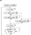
- FIG. 17 is a flowchart for explaining the control of the switch 41 by the control unit 72 of FIG.
- step S11 the control unit 72 turns on the switch 41, and the process proceeds to step S12.
- step S12 the control unit 72 determines whether or not the magnitude (absolute value)
- step S12 If it is determined in step S12 that the magnitude
- step S12 when it is determined in step S12 that the magnitude
- step S13 when it is determined that the magnitude
- step S13 When it is determined in step S13 that the magnitude
- of the current i 1 rises from 0 A over the threshold value TH11, and then falls below the threshold value TH11.
- step S12 the magnitude of the current i 1
- step S15 the control unit 72 determines whether the time t CLK / 2 has elapsed since the previous switch 41 was turned on.
- step S15 If it is determined in step S15 that the time t CLK / 2 has not yet elapsed since the previous switch 41 was turned on, the processing returns to step S15.
- step S15 If it is determined in step S15 that the time t CLK / 2 has elapsed since the previous switch 41 was turned on, the process returns to step S11, the control unit 72 turns on the switch 41, and so on. The process is repeated.
- FIG. 18 is a circuit diagram showing a fourth configuration example of the gate drive circuit 31 of FIG.
- the gate drive circuit 31 in FIG. 18 includes a coil L g , a switch 41, a switch 51, a control unit 52, a resistor 53, a DC power supply 54, an offset circuit 60, a current detection unit 71, and a control unit 72. This is common to 15 of the third configuration example.
- the gate drive circuit 31 of FIG. 18 has a coil 73, and the current detection unit 71 detects the current i 1 (current value) flowing in the coil L g based on the current flowing in the coil 73. 15 different from the third configuration example.
- the gate drive circuit 31 in FIG. 18 adaptively controls the switching of the switch 41, so that the resonance period 2 ⁇ of the L g Ciss resonance circuit is not provided without providing a trimmer capacitor. Deal with changes in ⁇ (L g C iss ).
- the coil 73 is provided in the vicinity of the coil L g , and accordingly, a current proportional to the current i 1 flowing through the coil L g flows through the coil 73 due to electromagnetic induction.
- the current detection unit 71 detects a current flowing through the coil 73, detects a current i 1 (current value) flowing through the coil L g based on the current, and supplies it to the control unit 72.
- the control unit 72 supplies the control signal C1 to the switch 41, thereby controlling the switch 41 (on / off) as in the case described with reference to FIGS.
- FIG. 19 is a circuit diagram showing a fifth configuration example of the gate drive circuit 31 of FIG.
- the gate drive circuit 31 of FIG. 19 is common to the second configuration example of FIG. 12 in that it includes a coil L g , a switch 41, a switch 51, a control unit 52, a resistor 53, a DC power supply 54, and an offset circuit 60. To do.
- the gate drive circuit 31 of FIG. 19 is provided with a voltage detection unit 81 and is provided with a control unit 82 instead of the control unit 42.
- the second configuration example of FIG. Is different.
- the voltage detector 81 detects the gate voltage (value) and supplies it to the controller 82.
- the control unit 82 controls the switch 41 (on and off) by supplying the control signal C1 to the switch 41, similarly to the control unit 42 of FIG.
- control unit 82 as a period corresponding to the period t CLK for switching the FET 33, for example, on a half of the period t CLK / 2 period t CLK, then, is supplied from the voltage detecting unit 81
- the switch 41 is controlled so as to be turned off in accordance with the gate voltage.
- FIG. 20 shows the on / off state of the switch 51 (control signal C2), the current i 2 that flows when the switch 51 is turned on / off, and the on / off state of the switch 41 for the gate drive circuit 31 of FIG.
- FIG. 4 is a waveform diagram showing a control signal C1), a current i 1 that flows when a switch 41 is turned on and off, and a gate voltage.
- control signal C2 The on / off state of the switch 51 (control signal C2) and the current i 2 that flows when the switch 51 is turned on / off are the same as those described with reference to FIGS.
- the switch 41 (control signal C1) is turned on at the cycle t CLK / 2.
- the control unit 82 adaptively turns off the switch 41 based on the gate voltage detected by the voltage detection unit 81.
- the gate voltage Under the control of the control unit 82, after the switch 41 is turned on, the gate voltage has a first threshold value TH21 (below) as a predetermined threshold value or a second threshold value TH22 (greater than the first threshold value TH21). It will be turned off.
- the switch 41 is turned on, from time t 21 immediately before the current i 1 starts to flow, L g C iss resonance period of the resonance circuit 2 ?? 1/2 of (L g C iss)
- L g C iss resonance period of the resonance circuit 2 ?? 1/2 of (L g C iss)
- first threshold TH21 by setting the 0V, the gate voltage, the timing became 0V is first threshold TH21 is, from the time t 21 immediately before the current i 1 starts to flow, L g C
- the iss resonance circuit has a resonance period of 2 ⁇ (L g C iss ), and at that timing, the switch 41 is turned off and the gate voltage is also the first threshold TH21.
- the voltage should be fixed at 0V, which is the minimum value.
- a value obtained by taking a margin to 0 V which is the minimum value of the gate voltage, that is, a small positive value close to 0 V is set as the first threshold TH21 of the gate voltage, and the control unit 82 When the gate voltage reaches the first threshold value TH21, a half time of the resonance period 2 ⁇ (L g C iss ) of the L g C iss resonant circuit has elapsed since the current i 1 began to flow. Then, the switch 41 is controlled to be turned off.
- the switch 41 is turned on, from the time t 23 immediately before the current i 1 starts to flow, L g C iss resonance period of the resonance circuit 2 ?? 1/2 of (L g C iss)
- L g C iss resonance period of the resonance circuit 2 ?? 1/2 of (L g C iss)
- the current i 1 flows when the gate voltage becomes + V DD which is the second threshold TH22.
- This is the timing when 1/2 of the resonance period 2 ⁇ (L g C iss ) of the L g C iss resonant circuit has elapsed since time t 23 immediately before the start, and at that timing, the switch 41 is turned off and the gate Ideally, the voltage is fixed at + V DD which is the maximum value of the gate voltage, which is also the second threshold TH22.
- the maximum value a is + V DD value taking the margin of the gate voltage, i.e., close to the + V DD, the following values + V DD, a second threshold value TH22 of the gate voltage
- the control unit 82 sets the resonance period 2 ⁇ (L g C iss ) of the L g C iss resonance circuit after the current i 1 starts flowing when the gate voltage reaches the second threshold TH22. Assuming that the time of / 2 has elapsed, the switch 41 is controlled to be turned off.
- FIG. 21 is a flowchart for explaining the control of the switch 41 by the control unit 82 of FIG.
- step S21 the control unit 82 turns on the switch 41, and the process proceeds to step S22.
- step S22 the control unit 82 is detected by the voltage detection unit 81 determines whether or not the gate voltage v GS at the on-switch 41 is less than or equal to the first threshold value TH21.
- step S22 the gate voltage v GS at the ON time of the switch 41, when it is determined to be equal to or less than the first threshold value TH21, the process proceeds to step S23, the control unit 82 is detected by the voltage detection unit 81 It is determined whether or not the gate voltage v GS is equal to or higher than the second threshold value TH22.
- step S23 when the gate voltage v GS is determined not to have been the second threshold value TH22 above, the processing returns to step S23.
- step S23 If it is determined in step S23 that the gate voltage v GS has become equal to or higher than the second threshold TH22, the process proceeds to step S24, and the control unit 82 determines that L g after the switch 41 is turned on. Assuming that a time of 1/2 of the resonance period 2 ⁇ (L g C iss ) of the C iss resonance circuit has elapsed, the switch 41 is turned off and the process proceeds to step S25.
- step S22 the gate voltage v GS at the ON time of the switch 41, when it is determined that the first not threshold TH21 less, the process proceeds to step S26, the control unit 82, detected by the voltage detection unit 81 It is determined whether the gate voltage v GS to be applied is equal to or lower than the first threshold value TH21.
- step S26 when the gate voltage v GS is determined not to have been below a first threshold value TH21, the process returns to step S26.
- step S26 If it is determined in step S26 that the gate voltage v GS has become equal to or lower than the first threshold TH21, the process proceeds to step S24, and as described above, the control unit 82 turns on the switch 41. Then, assuming that the time of 1/2 of the resonance period 2 ⁇ (L g C iss ) of the L g C iss resonance circuit has elapsed, the switch 41 is turned off, and the process proceeds to step S25.
- the gate voltage v GS is the first threshold TH11 (or lower) or the second threshold TH22 (or higher).
- the gate voltage increases from the first threshold TH11 (or lower) or decreases from the second threshold TH22 (or higher).
- the timing to turn off the switch 41, the gate voltage v GS is increased from the first threshold value TH11 (or less), and when it becomes the second threshold value TH22, falling from the second threshold value TH22 (higher) This is when the first threshold value TH21 is reached.
- step S22 the gate voltage v GS at the ON time of the switch 41, after which it is less than the first threshold value TH21 is confirmed (determined) in step S23, the gate voltage v GS is, It is determined whether or not the first threshold value TH21 or lower has increased to the second threshold value TH22 (or higher), that is, whether or not it is time to turn off the switch 41.
- step S22 the gate voltage v GS at the ON time of the switch 41, when it is determined that the first not the threshold TH21 less, the gate voltage v GS at the ON time of the switch 41 and the second Since the threshold TH22 (or above) is (should), the gate voltage v GS has subsequently dropped from the second threshold TH22 or above to the first threshold TH21 (or below) in step S26. That is, it is determined whether it is time to turn off the switch 41.
- step S25 the controller 82 determines whether or not the time t CLK / 2 has elapsed since the previous switch 41 was turned on.
- step S25 If it is determined in step S25 that the time t CLK / 2 has not yet elapsed since the previous switch 41 was turned on, the process returns to step S25.
- step S25 If it is determined in step S25 that the time t CLK / 2 has elapsed since the previous switch 41 was turned on, the process returns to step S21, the control unit 82 turns on the switch 41, and so on. The process is repeated.
- the gate drive circuit 31 of FIGS. 15 and 18 controls the switch 41 according to the current i 1 flowing through the coil L g, and the gate drive circuit 31 of FIG. 19 controls the switch 41 according to the gate voltage.
- the gate drive circuit 31 shown in FIGS. 15 and 18 is different from the gate drive circuit 31 shown in FIG. 19 in terms of control.
- the gate drive circuit 31 of FIGS. 15 and 18 consumes the power regenerated by the L g Ciss resonance circuit to detect (measure) the current i 1 flowing through the coil L g .
- the threshold value TH11 (+ TH11 and -TH11) may be set to a small positive value close to 0A, and can be set relatively easily.
- the first threshold value TH21 and the second threshold value TH22 of the gate voltage are set to values obtained by taking a certain margin from the minimum value and the maximum value of the gate voltage, respectively.
- the margin taken to the first threshold value TH21 and the second threshold value TH22 of the gate voltage, directly affects the power of the power loss is regenerated by L g C iss resonant circuit. That is, the gate voltage is lowered to a first threshold value TH21, or, when raised to a second threshold value TH22, the switch 41 is turned off, the current i 1 does not flow, the gate voltage, the minimum Until the value becomes 0V or the maximum value + V DD , no charge is accumulated in the input capacitance C iss (not fully charged).
- the gate drive circuit 31 of FIG. 19 the voltage detecting section 81, L g C iss hardly affects the Q value of the resonant circuit (Quality Factor), due to the voltage detection unit 81, L g C iss resonant circuit There is almost no loss of power regenerated in
- a PMOS FET can be adopted instead of an NMOS FET. The same applies to the FETs 32, 34, and 35.
- the gate drive circuit 31 of FIGS. 15, 18, and 19 is provided with the offset circuit 60.
- the gate drive circuit 31 of FIGS. 15, 18, and 19 is provided.
- the offset circuit 60 can be omitted.
- the series of processes of the control units 42, 52, 72, and 82 described above can be performed by hardware or can be performed by software.
- a program constituting the software is installed in a computer (processor) such as a microcomputer.
- FIG. 22 shows a configuration example of an embodiment of a computer in which a program for executing the series of processes described above is installed.
- the program can be recorded in advance in a hard disk 105 or a ROM 103 as a recording medium built in the computer.
- the program can be stored (recorded) in the removable recording medium 111.
- a removable recording medium 111 can be provided as so-called package software.
- examples of the removable recording medium 111 include a flexible disk, a CD-ROM (Compact Disc Read Only Memory), an MO (Magneto Optical) disc, a DVD (Digital Versatile Disc), a magnetic disc, and a semiconductor memory.
- the program can be installed on the computer from the removable recording medium 111 as described above, or can be downloaded to the computer via the communication network or the broadcast network and installed on the built-in hard disk 105. That is, the program is transferred from a download site to a computer wirelessly via a digital satellite broadcasting artificial satellite, or wired to a computer via a network such as a LAN (Local Area Network) or the Internet. be able to.
- a network such as a LAN (Local Area Network) or the Internet.
- the computer includes a CPU (Central Processing Unit) 102, and an input / output interface 110 is connected to the CPU 102 via the bus 101.
- CPU Central Processing Unit
- the CPU 102 executes a program stored in a ROM (Read Only Memory) 103 accordingly. .
- the CPU 102 loads a program stored in the hard disk 105 into a RAM (Random Access Memory) 104 and executes it.
- the CPU 102 performs processing according to the flowchart described above or processing performed by the configuration of the block diagram described above. Then, the CPU 102 outputs the processing result as necessary, for example, via the input / output interface 110, from the output unit 106, transmitted from the communication unit 108, and further recorded in the hard disk 105.
- the input unit 107 includes a keyboard, a mouse, a microphone, and the like.
- the output unit 106 includes an LCD (Liquid Crystal Display), a speaker, and the like.
- the processing performed by the computer according to the program does not necessarily have to be performed in chronological order in the order described as the flowchart. That is, the processing performed by the computer according to the program includes processing executed in parallel or individually (for example, parallel processing or object processing).
- the program may be processed by one computer (processor), or may be distributedly processed by a plurality of computers. Furthermore, the program may be transferred to a remote computer and executed.
- the system means a set of a plurality of components (devices, modules (parts), etc.), and it does not matter whether all the components are in the same housing. Accordingly, a plurality of devices housed in separate housings and connected via a network and a single device housing a plurality of modules in one housing are all systems. .
- the present technology can take a cloud computing configuration in which one function is shared by a plurality of devices via a network and is jointly processed.
- each step described in the above flowchart can be executed by one device or can be shared by a plurality of devices.
- the plurality of processes included in the one step can be executed by being shared by a plurality of apparatuses in addition to being executed by one apparatus.
- this technique can take the following structures.
- the offset circuit is Other DC power supplies having a voltage half that of the DC power supply, A resistor for biasing the gate voltage of the FET;
- the offset circuit is One end of the resistor is connected to the positive terminal of the other DC power source, One end of the capacitor is connected to the other end of the resistor, A negative terminal of the other DC power source is connected to the other end of the capacitor;
- the drive circuit according to [3] wherein one end of the coil whose one end is connected to the gate of the FET is connected to a connection point between the resistor and the capacitor.
- a voltage detector for detecting the voltage of the gate of the FET A first switch control unit that controls the first switch so that the FET is turned on in a cycle corresponding to a cycle for switching the FET and is turned off in accordance with a voltage detected by the voltage detection unit.
- the first switch of the FET drive circuit comprising a second switch for turning on or off the connection between the DC power source and the gate of the FET is temporarily turned on in a cycle corresponding to the cycle for switching the FET.
- the driving method in which the second switch is periodically turned on for a predetermined period of the period in which the first switch is off.
Landscapes
- Engineering & Computer Science (AREA)
- Power Engineering (AREA)
- Computer Networks & Wireless Communication (AREA)
- Power Conversion In General (AREA)
- Charge And Discharge Circuits For Batteries Or The Like (AREA)
- Dc-Dc Converters (AREA)
Abstract
La présente invention porte sur un circuit de commande et un procédé de commande dans lesquels, au moyen d'un circuit simple, des pertes lors de la commutation de FET peuvent être réduites. Une bobine et une capacité d'entrée de grille de FET forment ensemble un circuit de résonance. Un commutateur (commutateur de régénération) autorise ou coupe le courant qui circule vers la bobine. Une source de puissance à courant continu pour alimenter une charge électrique sur le circuit de résonance est connectée à la grille de FET. Un commutateur (commutateur d'alimentation) autorise ou coupe la connexion entre la source de puissance à courant continu et la grille de FET. La présente invention peut être appliquée à des sources de puissance qui fournissent un courant et une tension à courant alternatif au moyen d'une commutation, par exemple.
Priority Applications (4)
| Application Number | Priority Date | Filing Date | Title |
|---|---|---|---|
| US14/412,839 US9356596B2 (en) | 2012-07-12 | 2013-07-02 | Driving circuit and driving method |
| EP13817437.0A EP2874294B1 (fr) | 2012-07-12 | 2013-07-02 | Circuit de commande et procédé de commande |
| CN201380035841.XA CN104412499B (zh) | 2012-07-12 | 2013-07-02 | 驱动器电路和驱动方法 |
| US15/144,511 US9509302B2 (en) | 2012-07-12 | 2016-05-02 | Driving circuit and driving method |
Applications Claiming Priority (2)
| Application Number | Priority Date | Filing Date | Title |
|---|---|---|---|
| JP2012156199A JP5915428B2 (ja) | 2012-07-12 | 2012-07-12 | 駆動回路、及び、駆動方法 |
| JP2012-156199 | 2012-07-12 |
Related Child Applications (2)
| Application Number | Title | Priority Date | Filing Date |
|---|---|---|---|
| US14/412,839 A-371-Of-International US9356596B2 (en) | 2012-07-12 | 2013-07-02 | Driving circuit and driving method |
| US15/144,511 Continuation US9509302B2 (en) | 2012-07-12 | 2016-05-02 | Driving circuit and driving method |
Publications (1)
| Publication Number | Publication Date |
|---|---|
| WO2014010459A1 true WO2014010459A1 (fr) | 2014-01-16 |
Family
ID=49915922
Family Applications (1)
| Application Number | Title | Priority Date | Filing Date |
|---|---|---|---|
| PCT/JP2013/068082 WO2014010459A1 (fr) | 2012-07-12 | 2013-07-02 | Circuit de commande et procédé de commande |
Country Status (5)
| Country | Link |
|---|---|
| US (2) | US9356596B2 (fr) |
| EP (1) | EP2874294B1 (fr) |
| JP (1) | JP5915428B2 (fr) |
| CN (1) | CN104412499B (fr) |
| WO (1) | WO2014010459A1 (fr) |
Families Citing this family (8)
| Publication number | Priority date | Publication date | Assignee | Title |
|---|---|---|---|---|
| US9948289B2 (en) * | 2015-06-02 | 2018-04-17 | Infineon Technologies Austria Ag | System and method for a gate driver |
| US10211827B2 (en) * | 2017-01-31 | 2019-02-19 | Ford Global Technologies, Llc | Resonant gate driver |
| CN107454993B (zh) | 2017-07-19 | 2020-10-23 | 深圳市汇顶科技股份有限公司 | 电源产生电路、电容式阵列传感装置和终端设备 |
| US10477686B2 (en) * | 2017-07-26 | 2019-11-12 | Canon Kabushiki Kaisha | Printed circuit board |
| US10355688B2 (en) | 2017-12-06 | 2019-07-16 | Silanna Asia Pte Ltd | Controlled current manipulation for regenerative charging of gate capacitance |
| JP7071193B2 (ja) * | 2018-03-30 | 2022-05-18 | キヤノン株式会社 | 送電装置 |
| WO2020223061A1 (fr) * | 2019-04-29 | 2020-11-05 | Efficient Power Conversion Corporation | Fet d'attaque de diode laser gan avec réutilisation de courant de grille |
| CN111390412A (zh) * | 2020-03-06 | 2020-07-10 | 重庆大学 | 一种大电流电磁脉冲焊接装置 |
Citations (6)
| Publication number | Priority date | Publication date | Assignee | Title |
|---|---|---|---|---|
| JP2002223157A (ja) * | 2001-01-25 | 2002-08-09 | Toyota Industries Corp | Mosfet等の電圧駆動型トランジスタの駆動回路 |
| JP2005039988A (ja) * | 2003-07-02 | 2005-02-10 | Denso Corp | ゲート駆動回路 |
| JP2006054954A (ja) | 2004-08-11 | 2006-02-23 | Toshiba Corp | 電力用mosfetのゲート駆動回路及びゲート駆動方法 |
| JP2009016997A (ja) * | 2007-07-02 | 2009-01-22 | Calsonic Kansei Corp | スイッチング回路 |
| JP2011130571A (ja) * | 2009-12-17 | 2011-06-30 | Denso Corp | 電力変換回路の制御装置 |
| JP2012034079A (ja) * | 2010-07-29 | 2012-02-16 | Fuji Electric Co Ltd | 絶縁ゲート型デバイスの駆動回路 |
Family Cites Families (5)
| Publication number | Priority date | Publication date | Assignee | Title |
|---|---|---|---|---|
| FR2649841B1 (fr) * | 1989-07-17 | 1994-10-14 | Sgs Thomson Microelectronics | Circuit de commande de grille d'un transistor mos |
| US5010261A (en) * | 1989-12-08 | 1991-04-23 | General Electric Company | Lossless gate driver circuit for a high frequency converter |
| US6570777B1 (en) * | 2001-12-06 | 2003-05-27 | Eni Technology, Inc. | Half sine wave resonant drive circuit |
| CN1849748B (zh) * | 2003-09-08 | 2011-05-11 | 皇家飞利浦电子股份有限公司 | 半导体开关的高频控制 |
| US8456201B2 (en) * | 2011-07-06 | 2013-06-04 | Eaton Corporation | Energy-recycling resonant drive circuits for semiconductor devices |
-
2012
- 2012-07-12 JP JP2012156199A patent/JP5915428B2/ja active Active
-
2013
- 2013-07-02 CN CN201380035841.XA patent/CN104412499B/zh active Active
- 2013-07-02 US US14/412,839 patent/US9356596B2/en active Active
- 2013-07-02 EP EP13817437.0A patent/EP2874294B1/fr active Active
- 2013-07-02 WO PCT/JP2013/068082 patent/WO2014010459A1/fr active Application Filing
-
2016
- 2016-05-02 US US15/144,511 patent/US9509302B2/en active Active
Patent Citations (6)
| Publication number | Priority date | Publication date | Assignee | Title |
|---|---|---|---|---|
| JP2002223157A (ja) * | 2001-01-25 | 2002-08-09 | Toyota Industries Corp | Mosfet等の電圧駆動型トランジスタの駆動回路 |
| JP2005039988A (ja) * | 2003-07-02 | 2005-02-10 | Denso Corp | ゲート駆動回路 |
| JP2006054954A (ja) | 2004-08-11 | 2006-02-23 | Toshiba Corp | 電力用mosfetのゲート駆動回路及びゲート駆動方法 |
| JP2009016997A (ja) * | 2007-07-02 | 2009-01-22 | Calsonic Kansei Corp | スイッチング回路 |
| JP2011130571A (ja) * | 2009-12-17 | 2011-06-30 | Denso Corp | 電力変換回路の制御装置 |
| JP2012034079A (ja) * | 2010-07-29 | 2012-02-16 | Fuji Electric Co Ltd | 絶縁ゲート型デバイスの駆動回路 |
Also Published As
| Publication number | Publication date |
|---|---|
| US9356596B2 (en) | 2016-05-31 |
| CN104412499A (zh) | 2015-03-11 |
| CN104412499B (zh) | 2017-06-09 |
| JP2014023172A (ja) | 2014-02-03 |
| EP2874294B1 (fr) | 2019-02-27 |
| EP2874294A1 (fr) | 2015-05-20 |
| US20160248421A1 (en) | 2016-08-25 |
| US9509302B2 (en) | 2016-11-29 |
| JP5915428B2 (ja) | 2016-05-11 |
| EP2874294A4 (fr) | 2016-11-30 |
| US20150155865A1 (en) | 2015-06-04 |
Similar Documents
| Publication | Publication Date | Title |
|---|---|---|
| JP5915428B2 (ja) | 駆動回路、及び、駆動方法 | |
| US7948720B2 (en) | Voltage regulator with transient recovery circuit | |
| JP5902401B2 (ja) | 電源装置、制御回路、電子機器及び電源の制御方法 | |
| KR101367607B1 (ko) | 동기형 dc-dc 컨버터 | |
| JP2007215259A (ja) | 駆動回路及びそれを用いたスイッチングレギュレータ | |
| US20140146238A1 (en) | Switching power supply device | |
| WO2007007539A1 (fr) | Regulateur de commutation du type abaisseur, circuit de commande de celui-ci et dispositif electronique l'utilisant | |
| JP2012034519A (ja) | 電源の制御回路、電子機器及び電源の制御方法 | |
| US20120105029A1 (en) | Switching regulator | |
| US20140176089A1 (en) | Phase shift circuit and power factor correction circuit including the same | |
| US8446213B2 (en) | Charge pump circuit, control method thereof, and semiconductor integrated circuit | |
| JP2017055627A (ja) | 半導体装置及びdc−dcコンバータ | |
| US20140285121A1 (en) | Modulation scheme for driving a piezo element | |
| US20140043005A1 (en) | Dc-dc converter and control method for the same | |
| US8947062B2 (en) | Power supply circuit | |
| JP6366436B2 (ja) | 電圧制御装置 | |
| JP5408978B2 (ja) | 超音波モータの速度制御装置及び速度制御方法 | |
| JP2008046358A (ja) | 液晶表示装置の駆動回路及び駆動装置 | |
| JP2007028698A (ja) | Dc−dcコンバータ | |
| JP4110153B2 (ja) | 振動型アクチュエータの駆動装置および振動型アクチュエータの駆動方法 | |
| JP2012039823A (ja) | スイッチングレギュレータの制御回路およびそれを利用したスイッチングレギュレータ、電子機器 | |
| CN216904672U (zh) | 电子设备 | |
| WO2016132714A1 (fr) | Dispositif et système de transmission de puissance électrique | |
| JP2016226079A (ja) | 電源回路及び車載用電源システム | |
| JP5799825B2 (ja) | Dc−dcコンバータ、半導体集積回路及びdc−dc変換方法 |
Legal Events
| Date | Code | Title | Description |
|---|---|---|---|
| 121 | Ep: the epo has been informed by wipo that ep was designated in this application |
Ref document number: 13817437 Country of ref document: EP Kind code of ref document: A1 |
|
| WWE | Wipo information: entry into national phase |
Ref document number: 2013817437 Country of ref document: EP |
|
| WWE | Wipo information: entry into national phase |
Ref document number: 14412839 Country of ref document: US |
|
| NENP | Non-entry into the national phase |
Ref country code: DE |