WO2014010459A1 - 駆動回路、及び、駆動方法 - Google Patents
駆動回路、及び、駆動方法 Download PDFInfo
- Publication number
- WO2014010459A1 WO2014010459A1 PCT/JP2013/068082 JP2013068082W WO2014010459A1 WO 2014010459 A1 WO2014010459 A1 WO 2014010459A1 JP 2013068082 W JP2013068082 W JP 2013068082W WO 2014010459 A1 WO2014010459 A1 WO 2014010459A1
- Authority
- WO
- WIPO (PCT)
- Prior art keywords
- switch
- fet
- gate
- turned
- voltage
- Prior art date
Links
- 238000000034 method Methods 0.000 title claims abstract description 42
- 239000003990 capacitor Substances 0.000 claims description 47
- 238000001514 detection method Methods 0.000 claims description 22
- 230000005669 field effect Effects 0.000 claims description 7
- 230000008929 regeneration Effects 0.000 abstract description 20
- 238000011069 regeneration method Methods 0.000 abstract description 20
- 238000010586 diagram Methods 0.000 description 40
- 230000008569 process Effects 0.000 description 26
- 230000005540 biological transmission Effects 0.000 description 19
- 238000005516 engineering process Methods 0.000 description 12
- 238000004088 simulation Methods 0.000 description 11
- 230000007423 decrease Effects 0.000 description 6
- 230000007246 mechanism Effects 0.000 description 5
- 230000008602 contraction Effects 0.000 description 4
- 230000005674 electromagnetic induction Effects 0.000 description 4
- 230000004907 flux Effects 0.000 description 4
- 238000004891 communication Methods 0.000 description 3
- 238000006073 displacement reaction Methods 0.000 description 3
- 230000006870 function Effects 0.000 description 3
- 239000004065 semiconductor Substances 0.000 description 3
- 230000000295 complement effect Effects 0.000 description 2
- 230000033001 locomotion Effects 0.000 description 2
- 238000009774 resonance method Methods 0.000 description 2
- 238000009825 accumulation Methods 0.000 description 1
- 230000008859 change Effects 0.000 description 1
- 230000003247 decreasing effect Effects 0.000 description 1
- 230000003111 delayed effect Effects 0.000 description 1
- 230000005484 gravity Effects 0.000 description 1
- 230000001771 impaired effect Effects 0.000 description 1
- 239000004973 liquid crystal related substance Substances 0.000 description 1
- 229910044991 metal oxide Inorganic materials 0.000 description 1
- 150000004706 metal oxides Chemical class 0.000 description 1
- 238000012986 modification Methods 0.000 description 1
- 230000004048 modification Effects 0.000 description 1
- 230000003287 optical effect Effects 0.000 description 1
- 230000001172 regenerating effect Effects 0.000 description 1
- 230000004044 response Effects 0.000 description 1
- 230000002441 reversible effect Effects 0.000 description 1
Images


Classifications
-
- H—ELECTRICITY
- H02—GENERATION; CONVERSION OR DISTRIBUTION OF ELECTRIC POWER
- H02J—CIRCUIT ARRANGEMENTS OR SYSTEMS FOR SUPPLYING OR DISTRIBUTING ELECTRIC POWER; SYSTEMS FOR STORING ELECTRIC ENERGY
- H02J7/00—Circuit arrangements for charging or depolarising batteries or for supplying loads from batteries
-
- H—ELECTRICITY
- H03—ELECTRONIC CIRCUITRY
- H03K—PULSE TECHNIQUE
- H03K17/00—Electronic switching or gating, i.e. not by contact-making and –breaking
- H03K17/51—Electronic switching or gating, i.e. not by contact-making and –breaking characterised by the components used
- H03K17/56—Electronic switching or gating, i.e. not by contact-making and –breaking characterised by the components used by the use, as active elements, of semiconductor devices
- H03K17/687—Electronic switching or gating, i.e. not by contact-making and –breaking characterised by the components used by the use, as active elements, of semiconductor devices the devices being field-effect transistors
-
- H02J5/005—
-
- H—ELECTRICITY
- H02—GENERATION; CONVERSION OR DISTRIBUTION OF ELECTRIC POWER
- H02J—CIRCUIT ARRANGEMENTS OR SYSTEMS FOR SUPPLYING OR DISTRIBUTING ELECTRIC POWER; SYSTEMS FOR STORING ELECTRIC ENERGY
- H02J50/00—Circuit arrangements or systems for wireless supply or distribution of electric power
- H02J50/10—Circuit arrangements or systems for wireless supply or distribution of electric power using inductive coupling
- H02J50/12—Circuit arrangements or systems for wireless supply or distribution of electric power using inductive coupling of the resonant type
-
- H—ELECTRICITY
- H02—GENERATION; CONVERSION OR DISTRIBUTION OF ELECTRIC POWER
- H02J—CIRCUIT ARRANGEMENTS OR SYSTEMS FOR SUPPLYING OR DISTRIBUTING ELECTRIC POWER; SYSTEMS FOR STORING ELECTRIC ENERGY
- H02J50/00—Circuit arrangements or systems for wireless supply or distribution of electric power
- H02J50/40—Circuit arrangements or systems for wireless supply or distribution of electric power using two or more transmitting or receiving devices
-
- H02J7/025—
-
- H—ELECTRICITY
- H03—ELECTRONIC CIRCUITRY
- H03K—PULSE TECHNIQUE
- H03K17/00—Electronic switching or gating, i.e. not by contact-making and –breaking
- H03K17/04—Modifications for accelerating switching
- H03K17/041—Modifications for accelerating switching without feedback from the output circuit to the control circuit
- H03K17/0412—Modifications for accelerating switching without feedback from the output circuit to the control circuit by measures taken in the control circuit
- H03K17/04123—Modifications for accelerating switching without feedback from the output circuit to the control circuit by measures taken in the control circuit in field-effect transistor switches
-
- H—ELECTRICITY
- H02—GENERATION; CONVERSION OR DISTRIBUTION OF ELECTRIC POWER
- H02J—CIRCUIT ARRANGEMENTS OR SYSTEMS FOR SUPPLYING OR DISTRIBUTING ELECTRIC POWER; SYSTEMS FOR STORING ELECTRIC ENERGY
- H02J7/00—Circuit arrangements for charging or depolarising batteries or for supplying loads from batteries
- H02J7/007—Regulation of charging or discharging current or voltage
- H02J7/00712—Regulation of charging or discharging current or voltage the cycle being controlled or terminated in response to electric parameters
-
- H—ELECTRICITY
- H03—ELECTRONIC CIRCUITRY
- H03K—PULSE TECHNIQUE
- H03K2217/00—Indexing scheme related to electronic switching or gating, i.e. not by contact-making or -breaking covered by H03K17/00
- H03K2217/009—Resonant driver circuits
Definitions
- the present technology relates to a drive circuit and a drive method, and more particularly, to a drive circuit and a drive method that can reduce a loss when switching a FET (Field Effect Transistor) with a simple circuit.
- FET Field Effect Transistor
- Wireless power supply requires a high-frequency power source that can output AC signals (voltage, current) such as a sine wave with a certain amount of power.
- a high-frequency power supply generally has a simple circuit configuration and high efficiency, and an inverter that generates a rectangular wave by switching operation. Used.
- a power MOS FET Metal Oxide Semiconductor Semiconductor FET
- a switching element that performs a switching operation.
- FIG. 1 is a diagram showing a configuration of an example of a portion that performs switching of a conventional inverter.
- the source of the FET 1 is grounded (connected to the ground), and the drain is connected to a terminal or a line (not shown) whose connection to the ground should be switched (ON / OFF).
- a pulse (gate pulse) output from the pulse output unit 2 is supplied to the gate of the FET 1, and the FET 1 (gate) is driven by a pulse output from the pulse output unit 2.
- the FET 1 is an nMOS (negative channel MOS) FET, which is turned on when the H (High) level is applied to the gate and is applied when the L (Low) level is applied (the H level is not applied). And) turn off.
- nMOS negative channel MOS
- the FET 1 performs a switching operation that turns on when the pulse output from the pulse output unit 2 is at the H (High) level and turns off when the pulse is at the L (Low) level.
- the FET 1 is required to be a power MOS FET having a small resistance (on-resistance) between the drain and the source in order to increase the efficiency of the inverter.
- FET 1 can be obtained from the pulse output unit 2 (driver) that outputs a pulse for driving FET 1 having such a large input capacitance C iss. A heavy capacitive load.
- Patent Document 1 proposes a gate drive circuit for a power MOS FET that reduces energy loss by storing current by flowing current through the coil and regenerating the energy.
- the present technology has been made in view of such a situation, and makes it possible to reduce a loss when switching an FET with a simple circuit.
- a driving circuit includes a coil that forms a resonance circuit together with an input capacitance of a gate of an FET (Field Effect Transistor), a first switch that turns on or off a current flowing through the coil, and a charge in the resonance circuit.
- the FET drive circuit includes a DC power source connected to the gate of the FET and a second switch that turns on or off the connection between the DC power source and the gate of the FET.
- the current flowing through the coil constituting the resonance circuit together with the input capacitance of the gate of the FET is turned on or off.
- a DC power supply for replenishing the resonance circuit with a charge is connected to the gate of the FET, and the connection is turned on or off.
- a driving method includes a coil that forms a resonance circuit together with an input capacitance of a gate of an FET (Field Effect Transistor), a first switch that turns on or off a current flowing through the coil, and a charge that is applied to the resonance circuit.
- the first switch of the FET drive circuit comprising: a DC power source connected to the gate of the FET, and a second switch for turning on or off the connection between the DC power source and the gate of the FET.
- Drive that is temporarily turned on in a cycle corresponding to the cycle for switching the FET, and the second switch is periodically turned on for a predetermined period of time during which the first switch is off. Is the method.
- the first switch for turning on or off the current flowing in the coil constituting the resonance circuit together with the input capacitance of the gate of the FET is temporarily turned on in a cycle corresponding to the cycle for switching the FET.
- the second switch for turning on or off the connection between the DC power source for replenishing electric charge to the resonance circuit and the gate of the FET is only for a predetermined period of the period in which the first switch is off. , Periodically turned on.
- the drive circuit may be an independent device or may be an internal block constituting one device.
- the loss when switching the FET can be reduced with a simple circuit.
- FIG. 2 is a block diagram illustrating a configuration example of a power transmission device 11.
- FIG. 3 is a circuit diagram illustrating a first configuration example of a gate drive circuit 31.
- FIG. It is a wave form diagram which shows the control signal C1 which the control part outputs, and the control signal C2 which the control part 52 outputs.
- a control signal C2 which is a waveform diagram illustrating the current i 2 flowing through the switch 51 is controlled in accordance with the control signal C2.
- Control signal C1 the current i 1 flows through the switch 41 is controlled in accordance with the control signal C1, and is a waveform diagram showing the gate voltage. It is a diagram illustrating the relationship between the current i 1 and the gate voltage. It is a figure explaining a response
- FIG. 5 is a waveform diagram showing a control signal C2, a current i 2 that flows when a switch 51 is turned on / off, a control signal C1, a current i 1 that flows when a switch 41 is turned on / off, and a gate voltage. It is a circuit diagram which shows the circuit used for simulation. 6 is a circuit diagram illustrating a third configuration example of the gate drive circuit 31.
- FIG. FIG. 5 is a waveform diagram showing a control signal C2, a current i 2 that flows when a switch 51 is turned on / off, a control signal C1, a current i 1 that flows when a switch 41 is turned on / off, and a gate voltage.
- 4 is a flowchart illustrating control of a switch 41 by a control unit 72.
- FIG. 6 is a circuit diagram illustrating a fourth configuration example of the gate drive circuit 31.
- FIG. 7 is a circuit diagram showing a fifth configuration example of the gate drive circuit 31.
- FIG. FIG. 5 is a waveform diagram showing a control signal C2, a current i 2 that flows when a switch 51 is turned on / off, a control signal C1, a current i 1 that flows when a switch 41 is turned on / off, and a gate voltage.
- 4 is a flowchart illustrating control of a switch 41 by a control unit 82.
- FIG. 18 is a block diagram illustrating a configuration example of an embodiment of a computer to which the present technology is applied.
- FIG. 2 is a block diagram illustrating a configuration example of an embodiment of a wireless power feeding system to which the present technology is applied.
- the wireless power feeding system includes a power transmitting device 11 and a power receiving device 12, and performs wireless power feeding by, for example, an electromagnetic induction method using a magnetic field or a magnetic field resonance method.
- the power transmission device 11 has a power transmission coil that is a coil for transmitting electric power using a magnetic field, and transmits electric power.
- the power receiving device 12 has a power receiving coil that is a coil for receiving power using a magnetic field, and receives power transmitted from the power transmitting device 11 when placed near the power transmitting device 11. .
- a set of, for example, a cradle as the power transmission apparatus 11 and a portable terminal such as a mobile phone as the power reception apparatus 12, or the power transmission apparatus 11 for example, a charging stand and a set of, for example, an electric vehicle as the power receiving device 12, a set of, for example, a TV rack and a TV (television receiver) as the power receiving device 12, as the power transmitting device 11.
- a charging stand and a set of, for example, an electric vehicle as the power receiving device 12 a set of, for example, a TV rack and a TV (television receiver) as the power receiving device 12, as the power transmitting device 11.
- FIG. 2 only one power receiving device 12 is illustrated as a power receiving device that receives power from one power transmitting device 11 by wireless power feeding. However, there are a plurality of power receiving devices that receive power by wireless power feeding. There may be.
- a wireless power feeding system having a plurality of power receiving devices, for example, by placing a plurality of portable terminals as a plurality of power receiving devices, for example, on a tray (charging tray) as the power transmitting device 11, the plurality of portable devices. You can charge your device at the same time.
- FIG. 3 is a block diagram illustrating a configuration example of the power transmission device 11 of FIG.
- the power transmission device 11 includes a high-frequency power source 20 and a resonance circuit 24, and functions as a power source that performs wireless power feeding.
- the high-frequency power source 20 includes a DC power source 21, a control unit 22, and a driver circuit 23, and functions as a power source that outputs a rectangular wave voltage and current as AC by switching.
- the DC power supply 21 supplies a predetermined DC voltage (current) to the driver circuit 23.
- the control unit 22 controls the driver circuit 23 (the gate drive circuit 31 thereof) and each block constituting the power transmission device 11.
- the driver circuit (inverter) 23 uses a DC voltage from the DC power supply 21 to drive the resonance circuit 24 and generate a magnetic flux in the power transmission coil L that constitutes the resonance circuit 24, thereby causing electromagnetic induction or magnetic resonance. In this method, power is transmitted.
- the resonance circuit 24 is a series resonance circuit including a power transmission coil L and a capacitor C, and is driven by the driver circuit 23.
- a magnetic flux magnetic field
- wireless power feeding is performed by which the power is transmitted to the power receiving device 12 by an electromagnetic induction method or a magnetic field resonance method. .
- the driver circuit 23 forms a full-bridge inverter, and includes a gate drive circuit 31 and NMOS FETs 32, 33, 34, and 35.
- the gate drive circuit 31 turns on or off (turns on or off) each of the FETs 32 to 35 by applying a predetermined voltage to the gates of the FETs 32 to 35 under the control of the control unit 22.
- FETs 32 to 35 are power MOS FETs and are turned on or off (turned on and off) according to the driving of the gate drive circuit 31.
- the drain of the FET 32 is connected to the DC power source 21, and accordingly, a predetermined DC voltage output from the DC power source 21 is applied to the drain of the FET 32.
- the source of the FET 32 is connected to the drain of the FET 33, and the source of the FET 33 is grounded (connected to the ground (GND)).
- FETs 34 and 35 are connected in the same manner as FETs 32 and 33.
- the drain of the FET 34 is connected to the DC power supply 21, and the source of the FET 34 is connected to the drain of the FET 35.
- the source of the FET 35 is grounded.
- one end of the resonance circuit 24 is connected to a connection point P1 between the source of the FET 32 and the drain of the FET 33, and the other end of the resonance circuit 24 is connected to a connection point P2 between the source of the FET 34 and the drain of the FET 35. ing.
- one end of the power transmission coil L and the capacitor C is connected in the resonance circuit 24.
- the other end of the capacitor C is connected to a connection point P1 between the source of the FET 32 and the drain of the FET 33, and the other end of the power transmission coil L is connected to a connection point P2 between the source of the FET 34 and the drain of the FET 35. .
- the gate driving circuit 31 applies a predetermined voltage to the gates of the FETs 32 to 35 at a predetermined timing in accordance with the control of the control unit 22, so that the FETs 32 to 35 are respectively connected. Control to turn on or off.
- the FETs 32 and 33 are turned on and off in a complementary manner and periodically, respectively.
- the FET 32 is alternately turned on and off periodically.
- the set of FETs 34 and 35 is turned on and off in a complementary manner to the set of FETs 32 and 33 and periodically.
- connection point P1 between the source of the FET 32 and the drain of the FET 33 becomes a predetermined direct current voltage output from the DC power source 21, for example, H (High) level, and the source of the FET 34 and the drain of the FET 35 are connected.
- the connection point P2 is a ground level, for example, an L (Low) level.
- a current flows in a direction from the connection point P1 to the connection point P2 via the capacitor C and the power transmission coil L.
- connection point P2 between the source of the FET 34 and the drain of the FET 35 becomes an H level that is a predetermined DC voltage output from the DC power supply 21, and the connection point P1 between the source of the FET 32 and the drain of the FET 33 is the ground. It becomes the L level which is the level of.
- a current flows in a direction from the connection point P2 toward the connection point P1 via the power transmission coil L and the capacitor C.
- the resonance circuit 24 is applied with an AC voltage (rectangular wave voltage) with a period in which the FETs 32 to 35 are turned on (or off), and an AC with a similar period is applied according to the application of the AC voltage. Current flows.
- AC voltage rectangular wave voltage
- the period in which the FETs 32 to 35 are turned on (or off) is the resonance period 2 ⁇ (LC) of the resonance circuit 24 composed of the power transmission coil L and the capacitor C, that is, the resonance frequency 1 / ( It is set to the reciprocal of 2 ⁇ (LC)).
- a full bridge inverter is used as the driver circuit 23.
- the driver circuit 23 for example, a circuit that performs switching (ON / OFF) of an FET such as a half bridge inverter is used. be able to.
- FIG. 4 is a circuit diagram showing a first configuration example of the gate drive circuit 31 of FIG.
- FIG. 4 illustrates a configuration example of a portion for driving, for example, the FET 33 in the gate drive circuit 31 of FIG.
- the parts that drive the FETs 32, 34, and 35 other than the FET 33 are configured in the same manner.
- the gate drive circuit 31 has a power regeneration mechanism that regenerates the power used to drive the FET in order to drive the power MOS FET (gate) of the capacitive load with high efficiency.
- the gate drive circuit 31 includes a coil (regeneration coil) L g , a switch (regeneration switch) 41, a control unit 42, a switch (replenishment switch) 51, a control unit 52, a resistor (current limiting resistor). ) 53 and a DC power supply 54.
- the coil L g constitutes the gate input capacitance (capacitor) with C iss of FET33 the (series) resonant circuit.
- Switch 41 (first switch), one end of the coil L g, is provided between the gate of the FET 33. Switch 41, the control of the control unit 42, i.e., in accordance with the control signal C1 supplied from the control unit 42, on or off, thereby turning on or off the current i 1 flowing through the coil L g.
- the current i 1 flowing through the coil L g is a coil L g, the direction of flow to the gate of the FET 33, as well as the positive direction, the reverse direction, a negative direction.
- the control unit 42 controls the switch 41 (on / off) by supplying a control signal (regeneration switch control signal) C1 to the switch 41.
- the switch 51 (second switch) is turned on or off in accordance with control from the control unit 52, that is, a control signal (supplementary switch control signal) C2 supplied from the control unit 52, whereby the DC power supply 54 and the FET 33 are turned on. Turn on or off the connection to the gate.
- the plus terminal of the DC power supply 54 is connected to the gate of the FET 33 via the resistor 53 and the switch 51, and the minus terminal of the DC power supply 54 is connected to the source of the FET 33.
- the controller 52 controls the switch 51 (on / off) by supplying the control signal C2 to the switch 51.
- the resistor 53 is a resistor for limiting the current i 2 flowing from the DC power source 54 when the switch 51 is turned on.
- One end of the resistor 53 is connected to the plus terminal of the DC power source 54, and the other end of the resistor 53 Is connected to the gate of the FET 33 via the switch 51.
- the current flowing from the DC power supply 54 (current flowing through the resistor 53) i 2 is set to the forward direction from the plus terminal of the DC power supply 54 to the gate of the FET 33 and vice versa.
- the direction is the negative direction.
- the DC power supply 54 is a power supply that outputs a predetermined DC voltage + V DD (> 0).
- the positive terminal of the DC power supply 54 is connected to the gate of the FET 33 via the resistor 53 and the switch 51, and the negative terminal of the DC power supply 54 is connected to the source of the FET 33. Therefore, when the switch 51 is turned on, the (direct current) voltage + V DD of the direct current power source 54 is applied to the gate of the FET 33.
- the voltage + V DD of the DC power supply 54 is a voltage sufficient to drive the FET 33 (a voltage greater than the voltage v gs between the gate and the source when the FET 33 is turned on). .
- the input capacitance C iss of the gate of the FET 33 is equivalently present in parallel between the gate and the source of the FET 33.
- the input capacitance C iss of the gate of the FET 33, the coil L g , the switch 41, and the control unit 42 regenerate the power used to drive the FET 33. Is configured.
- the gate of the input capacitance C iss of FET 33, the charge accumulation, the voltage of the gate (the voltage of the gate as seen from the source), the H level ing.
- the voltage of the gate of FET33 at this time i.e., the input capacitance C iss, referenced to the terminal connected to the source, the voltage of the terminal connected to the gate, for example, the voltage of the DC power supply 54 + Suppose that it is V DD .
- the switch 41 is turned on at the timing when the FET 33 should be turned off (switched) in accordance with the control of the control unit 42.
- switch 41 By switch 41 is turned on, the charge accumulated in the input capacitance C iss, the switches 41 and discharges through the coil L g, the coil L g, the current i corresponding to the electric charge discharged 1 flows in the negative direction.
- the FET 33 When the charge accumulated in the input capacitance C iss is discharged to some extent and the gate voltage falls below the voltage + V DD to a predetermined value (the gate voltage at which the FET 33 is turned on), the FET 33 is turned off.
- the coil L g when a current i 1 continues to flow, the input capacitance C iss, charges are accumulated, a reference voltage (input capacitance C iss gate, a terminal connected to the source of FET 33, When the polarity of the voltage of the terminal connected to the gate is reversed, that is, when the voltage of the gate of the FET 33 becomes the voltage ⁇ V DD , the current i 1 flowing through the coil L g becomes zero.
- Switch 41 under the control of the control unit 42, at the timing when the current i 1 flowing through the coil L g is 0, it turned off. Thereby, the voltage of the gate of the FET 33 is maintained at the voltage ⁇ V DD .
- the switch 41 is turned on at the timing when the FET 33 should be turned on (switched) in accordance with the control of the control unit 42.
- the coil L g when a current i 1 flows, electric energy corresponding to the current i 1 is accumulated in the coil L g.
- the FET 33 When the charge accumulated in the input capacitance C iss is discharged to some extent and the gate voltage rises from the voltage ⁇ V DD to a predetermined value or more, the FET 33 is turned on.
- Switch 41 under the control of the control unit 42, at the timing when the current i 1 flowing through the coil L g is 0, it turned off. As a result, the voltage of the gate of the FET 33 is maintained at the voltage + V DD .
- the switch 41 is turned on at the timing when the FET 33 should be turned off in accordance with the control of the control unit 42, and the same operation is repeated thereafter.
- power regeneration mechanism as the input capacitance C iss, coil L g, switches 41 and, the control unit 42, the electric energy (electric charge) accumulated in the input capacitance C iss, with its input capacitance C iss accumulated in the coil L g which constitutes a resonance circuit, the electric energy stored in the coil L g, by repeating to accumulate in the input capacitance C iss, it regenerates electric power used for driving the FET 33, the power Is again used to drive the FET 33.
- the switch 51 is temporarily turned on, for example, periodically (from off to on) according to the control of the control unit 52.
- the DC power supply 54 can be referred to as a power supply for replenishing electric charges (power), and the current i 2 flowing from the DC power supply 54 can be referred to as a replenishing current for replenishing charges (electric power).
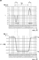
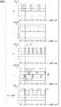
- FIG. 5 is a waveform diagram showing the control signal C1 output from the control unit 42 in FIG. 4 and the control signal C2 output from the control unit 52.
- control signals C1 and C2 are, for example, pulse signals that take binary values of L and H levels.
- the waveforms of the control signals C1 and C2 also represent the on and off states of the switches 41 and 51, respectively.
- the waveforms of the control signals C1 and C2 are appropriately switched on and off of the switches 41 and 51, respectively. It will be described as representing an off state.
- the switch 41 is turned on (temporarily) for the time t g with the period t CLK / 2 (the other period (time) is turned off).
- the control unit 52 periodically performs the period of time t s as a predetermined period of the period in which the switch 41 is off, that is, the period in which the control signal C1 is at the L level. A signal that becomes H level during this period and becomes L level during other periods is supplied to the switch 51 as the control signal C2.
- the switch 51 is turned on (temporarily) for the time t s during the period in which the switch 41 is turned off (the other period is turned off).
- control signal C2 which is a waveform diagram showing a current (supplemented current) i 2 flowing through the switch 51 is controlled in accordance with the control signal C2.
- Control signal C2 becomes H level, the switch 51 is turned on, from the DC power source 54, the current i 2 flows.
- the switch 51 is turned on for a time t s, the switch 51 is turned on, since a period in which the switch 41 is off, a current flows from the DC power source 54 i 2 (Charge) flows into the input capacitance C iss of the gate of the FET 33 through the resistor 53 and the switch 51 that is turned on.
- the electric charge is instantaneously accumulated in the input capacitance C iss of the gate of the FET 33 by the current i 2 flowing from the DC power supply 54 and then accumulated in the input capacitance C iss.
- the electric charge which decreases is decreasing rapidly.
- the switch 51 is turned on at a rate of once every two periods when the switch 41 is turned on, and the L g C iss resonance circuit including the input capacitance C iss and the coil L g. Charge is accumulated (supplemented) in the input capacitance C iss .
- the rate at which the switch 51 is turned on is not limited to the rate at which the switch 41 is turned on once every two cycles.
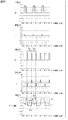
- FIG. 7 is a waveform diagram showing the control signal C1, the current (regeneration current) i 1 that flows when the switch 41 is controlled according to the control signal C1, and the gate voltage (the voltage at the gate of the FET 33).
- the switch 41 (control signal C1) is at a period t CLK / 2, by the time t g, turned on.
- the switch 51 is turned on during the period when the switch 41 is turned off. Therefore, at the time t g when the switch 41 is turned on, the switch 51 is turned off. It has become.
- the current i 1 in the negative direction flows only for the time t g when the switch 41 is on, so that charge is accumulated in the input capacitance C iss so that the gate voltage becomes (nearly) the negative voltage ⁇ V DD. Is done.
- the switch 41 is again by time t g, turned on, so that the gate voltage is a negative voltage -V DD, the charge accumulated in the input capacitance C iss, through the input capacitance C iss, coil
- the current i 1 flows through the L g C iss resonance circuit in the positive direction as shown in FIG.
- the current i 1 in the positive direction flows only for the time t g when the switch 41 is on, so that charge is accumulated in the input capacitance C iss so that the gate voltage becomes (approximately) the positive voltage + V DD. Is done.
- the gate voltage alternately becomes a positive voltage + V DD (H level) and a negative voltage ⁇ V DD (L level) every time t CLK / 2, and the FET 33 is switched at a period t CLK . Is done.
- FET 33 is in the period t CLK, by the time t CLK / 2, (becomes later, the time t CLK / 2 is off) to (temporarily) turned on.
- the time when the gate voltage is the positive voltage + V DD and the time when the gate voltage is the negative voltage ⁇ V DD are both the same at time t CLK / 2. , It becomes a pulse with a duty ratio of 50%.
- the duty ratio of the gate voltage is adjusted by shifting one of the two timing sets. can do.
- the gate voltage becomes a positive voltage + V DD at the first on-timing of a set of on-timing
- the period from the first on-timing to the second on-timing is The gate voltage is a positive voltage + V DD
- the period from the second on timing to the first on timing of the next on timing set is the negative voltage ⁇ V DD It will be a period.
- the second on-timing of the set of on-timing for example, the period during which the gate voltage becomes positive voltage + V DD and the period during which the negative voltage ⁇ V DD becomes negative are adjusted. That is, the duty ratio of the gate voltage can be adjusted.
- the switch 51 is turned on once every two cycles of the switch 41 being turned on, and the input capacitance C iss and the coil L the input capacitance C iss of composed L g C iss resonance circuit is g, the charge is replenished.
- the positive terminal of the DC power supply 54 is connected to the gate of the FET 33 (via the resistor 53 and the switch 51) and the positive voltage + V DD is applied.
- Replenishment of charge to the input capacitance C iss of the gate to which V DD is applied, that is, turning on the switch 51 (control signal C2), as shown in FIG. 7, has a positive gate voltage + V DD. It is performed at the timing of (H level).
- FIG. 8 is a diagram for explaining the relationship between the current i 1 and the gate voltage.
- the switch 41 is turned on, electric charge accumulated in the input capacitance C iss is the input capacitance C iss, switch 41, I'll be flowing in the order of coil L g (discharged), L g C iss A current i 1 represented by a sine wave having a resonance cycle 2 ⁇ (L g C iss ) of the resonance circuit flows in the coil L g in the negative direction (period T1).
- Switch 41 the last, after being turned on, when the period t CLK / 2 1/2 of the period t CLK for switching FET33 has elapsed, again, it is turned on.
- the electrical energy (charge) accumulated in the input capacitance C iss is accumulated in the coil L g constituting the L g C iss resonance circuit together with the input capacitance C iss , and the coil L the electrical energy stored in g, by repeating to accumulate in the input capacitance C iss, and power regeneration power used for driving the FET 33, the power is again used to drive the FET 33.
- FIG. 9 is a diagram for explaining the correspondence between the power regeneration of the gate drive circuit 31 and the vibration (movement) of the spring as dynamics.
- a weight is attached to the other end of the spring, the spring is extended or contracted by hand, and then the hand is released.
- the spring expands and contracts vertically (in a direction parallel to gravity), and the weight attached to the other end of the spring vibrates up and down (moves) as the spring expands and contracts.
- mechanical energy of the weight is represented by the formula kx 2/2 + mv 2/ 2.
- k represents the spring constant
- x is the weight position when the hand is released so that the weight is not vibrated by attaching a weight to the other end of the spring with one end fixed to the ceiling. Represents the position (displacement amount) of the weight.
- m represents the mass of the weight
- v represents the speed of the weight
- the speed v of the weight is 0 when the spring contraction is maximum with respect to the reference position and when the spring extension is maximum, that is, when the displacement amount x is maximum and minimum.
- C represents an input capacitance (capacitance) C iss
- V represents a voltage applied to the input capacitance C iss , that is, a gate voltage in the present embodiment.
- L is represents a coil (inductance) L g
- I represents the current i 1 flowing through the coil L g.
- FIG. 10 is a waveform diagram showing the currents i 1 and i 2 .
- the switch 41 is turned on by the time t g, only the time t g, by the current i 1 flows in the L g C iss resonant circuit, the polarity of the gate voltage of FET33 Is inverted (from one of H level and L level to the other).
- the amount of charge necessary for reversing the polarity of the gate voltage is a value obtained by integrating the current i 1 flowing through the L g C iss resonance circuit during the time t g .
- the DC power supply 54 can supply the electric energy to the other without receiving the supply of the electric energy from the outside, and the DC power supply 54 supplies the other.
- the electrical energy is only the current (replenishment current) i 2 for replenishing the input capacitance C iss of the L g C iss resonance circuit with power (charge).
- the current i 2 is a replenishment current for replenishing power lost as heat or the like, as shown in FIG. 10, the current i 2 is extremely smaller than the current i 1 .
- the amount of current required for driving (switching) the FET 33 is compared with the current i 1 from the amount of the current i 1 flowing through the L g C iss resonance circuit.
- the amount of current i 2 can be improved.
- the loss of power (charge) when switching the FET 33 can be greatly reduced from the power corresponding to the large current i 1 to the power corresponding to the small current i 2. .
- FIG. 11 is a circuit diagram showing a circuit (simulation circuit) used for the simulation for obtaining the waveform diagrams of FIGS. 5 to 8 and FIG.
- Simulation circuit instead of the FET33 of 4, except that the parallel circuit of the capacitor C G and a resistor R G to substitute for the gate of the FET33 is provided, similarly to the circuit shown in FIG. 4 It is configured.
- capacitor C G corresponds to the input capacitance C iss of the gate of the FET 33
- resistor R G corresponds to the input resistance of the gate of the FET 33.
- the resistor R G as an input resistance of the gate of the FET 33, since the resistance of very large resistance value, in the simulation circuit, such a large resistor R G can also be good (omitted without ).
- the FET is switched with a simple circuit configuration of the coil L g , the switch 41, the control unit 42, the switch 51, the control unit 52, the resistor 53, and the DC power supply 54.
- the loss of electric power (charge) can be reduced.
- FIG. 12 is a circuit diagram showing a second configuration example of the gate drive circuit 31 of FIG.
- the gate drive circuit 31 in FIG. 12 includes the coil L g , the switch 41, the control unit 42, the switch 51, the control unit 52, the resistor 53, and the DC power supply 54. And in common.
- the gate drive circuit 31 of FIG. 12 is different from the first configuration example of FIG. 4 in that a (DC voltage) offset circuit 60 is newly provided.
- the offset circuit 60 includes a DC power supply 61, a resistor (bias resistor) 62, and a capacitor (bypass capacitor) 63, and offsets the gate voltage of the FET 33 to a voltage equal to or higher than a predetermined value.
- the gate voltage of the FET 33 is changed from the voltage + V DD which is the voltage of the DC power supply 54 to the sign of the voltage + V DD .
- the voltage is in the range up to -V DD , which is reversed.
- a negative voltage may not be expected to be applied to the gate of the NMOS FET, and if the negative voltage -V DD is less than the guaranteed performance voltage that guarantees the performance of the FET, The reliability of the gate drive circuit 31 may be impaired.
- the offset circuit 60 offsets the gate voltage of the FET 33 to a predetermined value, for example, a voltage of 0 V or more.
- the gate voltage is offset so as to be a voltage in the range from the voltage + V DD which is the voltage of the DC power supply 54 to 0V.
- the DC power supply 61 the DC voltage + V DD to the DC power source 54 is outputted, for example, a power source for outputting a 1/2 of the DC voltage + V DD / 2.
- a plus terminal of the DC power supply 61 is connected to one end of the resistor 62, and a minus terminal of the DC power supply 61 is connected to one end of the capacitor 63.
- the resistor 62 is a resistor for biasing one end of the coil L g that is not connected to the switch 41, and hence the gate of the FET 33. As described above, one end of the resistor 62 is connected to the positive terminal of the DC power supply 61, and the other end of the resistor 62 is connected to the other end of the capacitor 63.
- the capacitor 63 is a capacitor for bypassing the current flowing through the L g C iss resonance circuit. As described above, one end of the capacitor 63 is connected to the negative terminal of the DC power supply 61, and the other end of the capacitor 63 is connected to the other end of the resistor 62.
- connection point between the resistor 62 and the capacitor 63 of the offset circuit 60 configured as described above is one end of the coil L g not connected to the switch 41 (one end is connected to the gate of the FET 44 via the switch 41). It is connected to the other end) of the coil L g which is connected to the connection point between the DC power supply 61 and the capacitor 63, in the source (Fig. 12 FET 33, and is connected to also the ground).
- the current i 1 flows through the capacitor 63 (bypass) at the same timing as in the case of FIG.
- one end of the coil L g not connected to the switch 41 is biased to the voltage + V DD / 2 of the DC power supply 61, not 0V (ground level), and is applied to the coil L g .
- the applied voltage goes from + V DD to + V DD / 2.
- the current i 1 flowing through the coil L g is 1 ⁇ 2 that in the case of FIG. 4, and further, the gate of the FET 33 is biased by the voltage + V DD / 2 from the case of FIG.
- the gate voltage in FIG. 4 is a range in which the range of the gate voltage in FIG. 4 is halved and biased by the voltage + V DD / 2, that is, the range from the voltage + V DD to 0 V.
- FIG. 13 shows the on / off state of the switch 51 (control signal C2), the current i 2 that flows when the switch 51 is turned on / off, and the on / off state of the switch 41 for the gate drive circuit 31 of FIG.
- FIG. 4 is a waveform diagram showing a control signal C1), a current i 1 that flows when a switch 41 is turned on and off, and a gate voltage.
- the offset circuit 60 is provided for the on / off state of the switch 51 (control signal C2), the current i 2 that flows when the switch 51 is turned on / off, and the on / off state of the switch 41 (control signal C1). Even if it is, it is the same as the case described with reference to FIGS.
- the current i 1 that flows when the switch 41 is turned on / off is 1 ⁇ 2 that of the case described with reference to FIGS. 5 to 8.
- the coil L g one end of which is not connected to the switch 41 is biased to voltage + V DD / 2 of the DC power supply 61.
- the current i 1 flowing through the coil L g and thus the L g C iss resonance circuit is 1 ⁇ 2 that of FIG. 4, and the range of the gate voltage is also shown in FIG. In this case, the voltage is half the range from the voltage ⁇ V DD to the voltage + V DD .
- the gate voltage is also the voltage + V DD. / 2 is biased, after all, the range of the gate voltage, as shown in FIG. 13, the half of the range of the range from the voltage -V DD in the case of FIG. 4 to the voltage + V DD, the voltage + V DD The range is from 0V to voltage + V DD biased by / 2.
- FIG. 14 is a circuit diagram showing a circuit (simulation circuit) used for the simulation for obtaining the waveform diagram of FIG.
- Simulation circuit instead of the FET33 of FIG 12, except that the parallel circuit of the capacitor C G and a resistor R G to substitute for the gate of the FET33 is provided, similarly to the circuit shown in FIG. 12 It is configured.
- the capacitor C G corresponds to the input capacitance C iss of the gate of the FET 33
- resistor R G corresponds to the input resistance of the gate of the FET 33.
- the resistor RG may not be provided.
- FIG. 15 is a circuit diagram showing a third configuration example of the gate drive circuit 31 of FIG.
- the gate drive circuit 31 in FIG. 15 is common to the second configuration example in FIG. 12 in that it includes a coil L g , a switch 41, a switch 51, a control unit 52, a resistor 53, a DC power supply 54, and an offset circuit 60. To do.
- the gate drive circuit 31 of FIG. 15 is provided with a current detection unit 71 and a control unit 72 in place of the control unit 42, so that the second configuration example of FIG. Is different.
- the input capacitance of FET33 and (capacitance) C iss
- the inductance of the coil L g may fluctuate.
- the resonance period 2 ⁇ (L g C iss ) 2 ⁇ t g of the L g C iss resonance circuit changes, so the time during which the switch 41 is on t g , more specifically, the timing to be turned off after the switch 41 is turned on also changes.
- a trimmer capacitor is provided in parallel with the gate (input capacitance C iss ) of the FET 33, For each driver circuit 23 (individually), the resonance period of the L g C iss resonance circuit matches the resonance period 2 ⁇ (L g C iss ) determined by the input capacitance C iss and the coil L g assumed in advance. There is a way to adjust the trimmer capacitor.
- providing a trimmer capacitor to prevent changes in the resonance period 2 ⁇ (L g C iss ) of the L g C iss resonant circuit is not limited to the adjustment of the trimmer capacitor, the cost of providing the trimmer capacitor, and the mounting area. It is difficult to say that it is advantageous in terms of the above.
- L g C iss resonance period of the resonance circuit 2 ?? (L g Deal with changes in C iss ).
- the gate drive circuit 31 of FIG. 15 is advantageous in that it eliminates the labor, cost, mounting area, and the like required when providing a trimmer capacitor.
- the current detection unit 71 detects the current i 1 (current value) flowing through the coil L g and supplies it to the control unit 72.
- the control unit 72 controls the switch 41 (on and off) by supplying the control signal C1 to the switch 41, similarly to the control unit 42 of FIG.
- control unit 72 as a period corresponding to the period t CLK for switching the FET 33, for example, on a half of the period t CLK / 2 period t CLK, then, is supplied from the current detector 71
- the switch 41 is controlled so as to be turned off according to the current i 1 .
- FIG. 16 shows the ON / OFF state of the switch 51 (control signal C2), the current i 2 that flows when the switch 51 is turned ON / OFF, and the ON / OFF state of the switch 41 for the gate drive circuit 31 of FIG.
- FIG. 4 is a waveform diagram showing a control signal C1), a current i 1 that flows when a switch 41 is turned on and off, and a gate voltage.
- control signal C2 The on / off state of the switch 51 (control signal C2) and the current i 2 that flows when the switch 51 is turned on / off are the same as those described with reference to FIGS.
- the switch 41 (control signal C1) is turned on at the cycle t CLK / 2.
- the switch 41 is adaptively turned off based on the current i 1 to be turned on.
- the switch 41 is turned off when the magnitude of the current i 1 (absolute value
- the charge is accumulated in the input capacitor C iss so that the gate voltage becomes the voltage + V DD and the switch 41 is turned on at time t 11 .
- the charge is accumulated in the input capacitor C iss .
- Charge flows from the input capacitance C iss in the order of the switch 41 and the coil L g (discharged), so that a sine wave having a resonance period 2 ⁇ (L g C iss ) of the L g C iss resonance circuit in the current i 1 represented is, the coil L g, flows in the negative direction.
- the gate voltage becomes a voltage (bias voltage) + V DD / 2 biased by the offset circuit 60. Further, the current i 1 flowing through the coil L g tends to become 0 A, but the current i 1 continues to flow through the coil L g due to inertia.
- the switch 41 is turned on, from the time t 11 immediately before the current i 1 starts to flow, L g C iss resonance period of the resonance circuit 2 ?? 1/2 of (L g C iss) When time elapses, the current i 1 flowing through the coil L g becomes 0A.
- the predetermined threshold value if set to 0, the current i 1 is, the timing became 0 is a predetermined threshold value, from the time t 11 immediately before the current i 1 starts to flow, L g C iss resonant circuit This is the timing when half the time of the resonance period 2 ⁇ (L g C iss ) has elapsed.
- the input capacitance C iss Is stored (should be) so that the gate voltage is 0 V lower than the bias voltage + V DD / 2 by the voltage V DD / 2, so at that timing, the switch 41 is turned off and the gate Ideally, the voltage should be fixed at 0V.
- timing is delayed when an operation such as turning off the switch 41 is started after it is detected that the current i 1 has reached a predetermined threshold value of 0.
- a value obtained by taking a margin from 0A that is, a positive value + TH11 obtained from a small positive value TH11 close to 0A and a negative value ⁇ TH11 are set to a predetermined threshold value of the current i 1.
- the control unit 72 sets the resonance period 2 ⁇ (L g C iss of the L g C iss resonant circuit after the current i 1 starts flowing when the current i 1 becomes the threshold + TH11 or ⁇ TH11. ), The switch 41 is turned off.
- the charge is accumulated in the input capacitance C iss so that the gate voltage becomes (almost) 0V, and the L g C iss resonance circuit is opened by turning off the switch 41.
- the gate voltage is fixed at 0V as shown in FIG.
- the control unit 72 the current i 1 is, when it becomes a threshold value + TH11 or -TH11, from the start of the current i 1 flows, L g C iss resonance period of the resonance circuit 2 ⁇ of (L g C iss)
- the switch 41 is controlled to be turned off assuming that the time of 1/2 has elapsed.
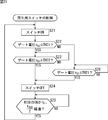
- FIG. 17 is a flowchart for explaining the control of the switch 41 by the control unit 72 of FIG.
- step S11 the control unit 72 turns on the switch 41, and the process proceeds to step S12.
- step S12 the control unit 72 determines whether or not the magnitude (absolute value)
- step S12 If it is determined in step S12 that the magnitude
- step S12 when it is determined in step S12 that the magnitude
- step S13 when it is determined that the magnitude
- step S13 When it is determined in step S13 that the magnitude
- of the current i 1 rises from 0 A over the threshold value TH11, and then falls below the threshold value TH11.
- step S12 the magnitude of the current i 1
- step S15 the control unit 72 determines whether the time t CLK / 2 has elapsed since the previous switch 41 was turned on.
- step S15 If it is determined in step S15 that the time t CLK / 2 has not yet elapsed since the previous switch 41 was turned on, the processing returns to step S15.
- step S15 If it is determined in step S15 that the time t CLK / 2 has elapsed since the previous switch 41 was turned on, the process returns to step S11, the control unit 72 turns on the switch 41, and so on. The process is repeated.
- FIG. 18 is a circuit diagram showing a fourth configuration example of the gate drive circuit 31 of FIG.
- the gate drive circuit 31 in FIG. 18 includes a coil L g , a switch 41, a switch 51, a control unit 52, a resistor 53, a DC power supply 54, an offset circuit 60, a current detection unit 71, and a control unit 72. This is common to 15 of the third configuration example.
- the gate drive circuit 31 of FIG. 18 has a coil 73, and the current detection unit 71 detects the current i 1 (current value) flowing in the coil L g based on the current flowing in the coil 73. 15 different from the third configuration example.
- the gate drive circuit 31 in FIG. 18 adaptively controls the switching of the switch 41, so that the resonance period 2 ⁇ of the L g Ciss resonance circuit is not provided without providing a trimmer capacitor. Deal with changes in ⁇ (L g C iss ).
- the coil 73 is provided in the vicinity of the coil L g , and accordingly, a current proportional to the current i 1 flowing through the coil L g flows through the coil 73 due to electromagnetic induction.
- the current detection unit 71 detects a current flowing through the coil 73, detects a current i 1 (current value) flowing through the coil L g based on the current, and supplies it to the control unit 72.
- the control unit 72 supplies the control signal C1 to the switch 41, thereby controlling the switch 41 (on / off) as in the case described with reference to FIGS.
- FIG. 19 is a circuit diagram showing a fifth configuration example of the gate drive circuit 31 of FIG.
- the gate drive circuit 31 of FIG. 19 is common to the second configuration example of FIG. 12 in that it includes a coil L g , a switch 41, a switch 51, a control unit 52, a resistor 53, a DC power supply 54, and an offset circuit 60. To do.
- the gate drive circuit 31 of FIG. 19 is provided with a voltage detection unit 81 and is provided with a control unit 82 instead of the control unit 42.
- the second configuration example of FIG. Is different.
- the voltage detector 81 detects the gate voltage (value) and supplies it to the controller 82.
- the control unit 82 controls the switch 41 (on and off) by supplying the control signal C1 to the switch 41, similarly to the control unit 42 of FIG.
- control unit 82 as a period corresponding to the period t CLK for switching the FET 33, for example, on a half of the period t CLK / 2 period t CLK, then, is supplied from the voltage detecting unit 81
- the switch 41 is controlled so as to be turned off in accordance with the gate voltage.
- FIG. 20 shows the on / off state of the switch 51 (control signal C2), the current i 2 that flows when the switch 51 is turned on / off, and the on / off state of the switch 41 for the gate drive circuit 31 of FIG.
- FIG. 4 is a waveform diagram showing a control signal C1), a current i 1 that flows when a switch 41 is turned on and off, and a gate voltage.
- control signal C2 The on / off state of the switch 51 (control signal C2) and the current i 2 that flows when the switch 51 is turned on / off are the same as those described with reference to FIGS.
- the switch 41 (control signal C1) is turned on at the cycle t CLK / 2.
- the control unit 82 adaptively turns off the switch 41 based on the gate voltage detected by the voltage detection unit 81.
- the gate voltage Under the control of the control unit 82, after the switch 41 is turned on, the gate voltage has a first threshold value TH21 (below) as a predetermined threshold value or a second threshold value TH22 (greater than the first threshold value TH21). It will be turned off.
- the switch 41 is turned on, from time t 21 immediately before the current i 1 starts to flow, L g C iss resonance period of the resonance circuit 2 ?? 1/2 of (L g C iss)
- L g C iss resonance period of the resonance circuit 2 ?? 1/2 of (L g C iss)
- first threshold TH21 by setting the 0V, the gate voltage, the timing became 0V is first threshold TH21 is, from the time t 21 immediately before the current i 1 starts to flow, L g C
- the iss resonance circuit has a resonance period of 2 ⁇ (L g C iss ), and at that timing, the switch 41 is turned off and the gate voltage is also the first threshold TH21.
- the voltage should be fixed at 0V, which is the minimum value.
- a value obtained by taking a margin to 0 V which is the minimum value of the gate voltage, that is, a small positive value close to 0 V is set as the first threshold TH21 of the gate voltage, and the control unit 82 When the gate voltage reaches the first threshold value TH21, a half time of the resonance period 2 ⁇ (L g C iss ) of the L g C iss resonant circuit has elapsed since the current i 1 began to flow. Then, the switch 41 is controlled to be turned off.
- the switch 41 is turned on, from the time t 23 immediately before the current i 1 starts to flow, L g C iss resonance period of the resonance circuit 2 ?? 1/2 of (L g C iss)
- L g C iss resonance period of the resonance circuit 2 ?? 1/2 of (L g C iss)
- the current i 1 flows when the gate voltage becomes + V DD which is the second threshold TH22.
- This is the timing when 1/2 of the resonance period 2 ⁇ (L g C iss ) of the L g C iss resonant circuit has elapsed since time t 23 immediately before the start, and at that timing, the switch 41 is turned off and the gate Ideally, the voltage is fixed at + V DD which is the maximum value of the gate voltage, which is also the second threshold TH22.
- the maximum value a is + V DD value taking the margin of the gate voltage, i.e., close to the + V DD, the following values + V DD, a second threshold value TH22 of the gate voltage
- the control unit 82 sets the resonance period 2 ⁇ (L g C iss ) of the L g C iss resonance circuit after the current i 1 starts flowing when the gate voltage reaches the second threshold TH22. Assuming that the time of / 2 has elapsed, the switch 41 is controlled to be turned off.
- FIG. 21 is a flowchart for explaining the control of the switch 41 by the control unit 82 of FIG.
- step S21 the control unit 82 turns on the switch 41, and the process proceeds to step S22.
- step S22 the control unit 82 is detected by the voltage detection unit 81 determines whether or not the gate voltage v GS at the on-switch 41 is less than or equal to the first threshold value TH21.
- step S22 the gate voltage v GS at the ON time of the switch 41, when it is determined to be equal to or less than the first threshold value TH21, the process proceeds to step S23, the control unit 82 is detected by the voltage detection unit 81 It is determined whether or not the gate voltage v GS is equal to or higher than the second threshold value TH22.
- step S23 when the gate voltage v GS is determined not to have been the second threshold value TH22 above, the processing returns to step S23.
- step S23 If it is determined in step S23 that the gate voltage v GS has become equal to or higher than the second threshold TH22, the process proceeds to step S24, and the control unit 82 determines that L g after the switch 41 is turned on. Assuming that a time of 1/2 of the resonance period 2 ⁇ (L g C iss ) of the C iss resonance circuit has elapsed, the switch 41 is turned off and the process proceeds to step S25.
- step S22 the gate voltage v GS at the ON time of the switch 41, when it is determined that the first not threshold TH21 less, the process proceeds to step S26, the control unit 82, detected by the voltage detection unit 81 It is determined whether the gate voltage v GS to be applied is equal to or lower than the first threshold value TH21.
- step S26 when the gate voltage v GS is determined not to have been below a first threshold value TH21, the process returns to step S26.
- step S26 If it is determined in step S26 that the gate voltage v GS has become equal to or lower than the first threshold TH21, the process proceeds to step S24, and as described above, the control unit 82 turns on the switch 41. Then, assuming that the time of 1/2 of the resonance period 2 ⁇ (L g C iss ) of the L g C iss resonance circuit has elapsed, the switch 41 is turned off, and the process proceeds to step S25.
- the gate voltage v GS is the first threshold TH11 (or lower) or the second threshold TH22 (or higher).
- the gate voltage increases from the first threshold TH11 (or lower) or decreases from the second threshold TH22 (or higher).
- the timing to turn off the switch 41, the gate voltage v GS is increased from the first threshold value TH11 (or less), and when it becomes the second threshold value TH22, falling from the second threshold value TH22 (higher) This is when the first threshold value TH21 is reached.
- step S22 the gate voltage v GS at the ON time of the switch 41, after which it is less than the first threshold value TH21 is confirmed (determined) in step S23, the gate voltage v GS is, It is determined whether or not the first threshold value TH21 or lower has increased to the second threshold value TH22 (or higher), that is, whether or not it is time to turn off the switch 41.
- step S22 the gate voltage v GS at the ON time of the switch 41, when it is determined that the first not the threshold TH21 less, the gate voltage v GS at the ON time of the switch 41 and the second Since the threshold TH22 (or above) is (should), the gate voltage v GS has subsequently dropped from the second threshold TH22 or above to the first threshold TH21 (or below) in step S26. That is, it is determined whether it is time to turn off the switch 41.
- step S25 the controller 82 determines whether or not the time t CLK / 2 has elapsed since the previous switch 41 was turned on.
- step S25 If it is determined in step S25 that the time t CLK / 2 has not yet elapsed since the previous switch 41 was turned on, the process returns to step S25.
- step S25 If it is determined in step S25 that the time t CLK / 2 has elapsed since the previous switch 41 was turned on, the process returns to step S21, the control unit 82 turns on the switch 41, and so on. The process is repeated.
- the gate drive circuit 31 of FIGS. 15 and 18 controls the switch 41 according to the current i 1 flowing through the coil L g, and the gate drive circuit 31 of FIG. 19 controls the switch 41 according to the gate voltage.
- the gate drive circuit 31 shown in FIGS. 15 and 18 is different from the gate drive circuit 31 shown in FIG. 19 in terms of control.
- the gate drive circuit 31 of FIGS. 15 and 18 consumes the power regenerated by the L g Ciss resonance circuit to detect (measure) the current i 1 flowing through the coil L g .
- the threshold value TH11 (+ TH11 and -TH11) may be set to a small positive value close to 0A, and can be set relatively easily.
- the first threshold value TH21 and the second threshold value TH22 of the gate voltage are set to values obtained by taking a certain margin from the minimum value and the maximum value of the gate voltage, respectively.
- the margin taken to the first threshold value TH21 and the second threshold value TH22 of the gate voltage, directly affects the power of the power loss is regenerated by L g C iss resonant circuit. That is, the gate voltage is lowered to a first threshold value TH21, or, when raised to a second threshold value TH22, the switch 41 is turned off, the current i 1 does not flow, the gate voltage, the minimum Until the value becomes 0V or the maximum value + V DD , no charge is accumulated in the input capacitance C iss (not fully charged).
- the gate drive circuit 31 of FIG. 19 the voltage detecting section 81, L g C iss hardly affects the Q value of the resonant circuit (Quality Factor), due to the voltage detection unit 81, L g C iss resonant circuit There is almost no loss of power regenerated in
- a PMOS FET can be adopted instead of an NMOS FET. The same applies to the FETs 32, 34, and 35.
- the gate drive circuit 31 of FIGS. 15, 18, and 19 is provided with the offset circuit 60.
- the gate drive circuit 31 of FIGS. 15, 18, and 19 is provided.
- the offset circuit 60 can be omitted.
- the series of processes of the control units 42, 52, 72, and 82 described above can be performed by hardware or can be performed by software.
- a program constituting the software is installed in a computer (processor) such as a microcomputer.
- FIG. 22 shows a configuration example of an embodiment of a computer in which a program for executing the series of processes described above is installed.
- the program can be recorded in advance in a hard disk 105 or a ROM 103 as a recording medium built in the computer.
- the program can be stored (recorded) in the removable recording medium 111.
- a removable recording medium 111 can be provided as so-called package software.
- examples of the removable recording medium 111 include a flexible disk, a CD-ROM (Compact Disc Read Only Memory), an MO (Magneto Optical) disc, a DVD (Digital Versatile Disc), a magnetic disc, and a semiconductor memory.
- the program can be installed on the computer from the removable recording medium 111 as described above, or can be downloaded to the computer via the communication network or the broadcast network and installed on the built-in hard disk 105. That is, the program is transferred from a download site to a computer wirelessly via a digital satellite broadcasting artificial satellite, or wired to a computer via a network such as a LAN (Local Area Network) or the Internet. be able to.
- a network such as a LAN (Local Area Network) or the Internet.
- the computer includes a CPU (Central Processing Unit) 102, and an input / output interface 110 is connected to the CPU 102 via the bus 101.
- CPU Central Processing Unit
- the CPU 102 executes a program stored in a ROM (Read Only Memory) 103 accordingly. .
- the CPU 102 loads a program stored in the hard disk 105 into a RAM (Random Access Memory) 104 and executes it.
- the CPU 102 performs processing according to the flowchart described above or processing performed by the configuration of the block diagram described above. Then, the CPU 102 outputs the processing result as necessary, for example, via the input / output interface 110, from the output unit 106, transmitted from the communication unit 108, and further recorded in the hard disk 105.
- the input unit 107 includes a keyboard, a mouse, a microphone, and the like.
- the output unit 106 includes an LCD (Liquid Crystal Display), a speaker, and the like.
- the processing performed by the computer according to the program does not necessarily have to be performed in chronological order in the order described as the flowchart. That is, the processing performed by the computer according to the program includes processing executed in parallel or individually (for example, parallel processing or object processing).
- the program may be processed by one computer (processor), or may be distributedly processed by a plurality of computers. Furthermore, the program may be transferred to a remote computer and executed.
- the system means a set of a plurality of components (devices, modules (parts), etc.), and it does not matter whether all the components are in the same housing. Accordingly, a plurality of devices housed in separate housings and connected via a network and a single device housing a plurality of modules in one housing are all systems. .
- the present technology can take a cloud computing configuration in which one function is shared by a plurality of devices via a network and is jointly processed.
- each step described in the above flowchart can be executed by one device or can be shared by a plurality of devices.
- the plurality of processes included in the one step can be executed by being shared by a plurality of apparatuses in addition to being executed by one apparatus.
- this technique can take the following structures.
- the offset circuit is Other DC power supplies having a voltage half that of the DC power supply, A resistor for biasing the gate voltage of the FET;
- the offset circuit is One end of the resistor is connected to the positive terminal of the other DC power source, One end of the capacitor is connected to the other end of the resistor, A negative terminal of the other DC power source is connected to the other end of the capacitor;
- the drive circuit according to [3] wherein one end of the coil whose one end is connected to the gate of the FET is connected to a connection point between the resistor and the capacitor.
- a voltage detector for detecting the voltage of the gate of the FET A first switch control unit that controls the first switch so that the FET is turned on in a cycle corresponding to a cycle for switching the FET and is turned off in accordance with a voltage detected by the voltage detection unit.
- the first switch of the FET drive circuit comprising a second switch for turning on or off the connection between the DC power source and the gate of the FET is temporarily turned on in a cycle corresponding to the cycle for switching the FET.
- the driving method in which the second switch is periodically turned on for a predetermined period of the period in which the first switch is off.
Abstract
本技術は、簡単な回路で、FETをスイッチングする際の損失を低減することができるようにする駆動回路、及び、駆動方法に関する。 コイルは、FETのゲートの入力容量とともに共振回路を構成する。スイッチ(回生用スイッチ)は、コイルに流れる電流をオン又はオフする。直流電源は、共振回路に電荷を補充するための電源であり、FETのゲートと接続される。スイッチ(補充用スイッチ)は、直流電源とFETのゲートとの接続をオン又はオフする。本技術は、例えば、スイッチングにより、交流の電圧及び電流を出力する電源に適用できる。
Description
本技術は、駆動回路、及び、駆動方法に関し、特に、簡単な回路で、FET(Field Effect Transistor)をスイッチングする際の損失を低減することができるようにする駆動回路、及び、駆動方法に関する。
近年、ワイヤレスで電力を供給するワイヤレス給電が注目されている。
ワイヤレス給電では、ある程度の電力の正弦波等の交流信号(電圧、電流)を出力することができる高周波電源が必要である。
大電力の正弦波の信号を、高効率で生成することは困難であるため、高周波電源としては、一般に、単純な回路構成で、高い効率が得られる、スイッチング動作により矩形波を生成するインバータが用いられる。
インバータにおいて、スイッチング動作を行うスイッチ素子としては、例えば、パワーMOS FET(Metal Oxide Semiconductor FET)が用いられる。
図1は、従来のインバータのスイッチングを行う部分の一例の構成を示す図である。
図1において、FET1のソースは、接地されており(グラウンドに接続されており)、ドレインは、グラウンドとの接続をスイッチング(オン、オフ)すべき図示せぬ端子や線に接続されている。
また、FET1のゲートには、パルス出力部2が出力するパルス(ゲートパルス)が供給されるようになっており、FET1(のゲート)は、パルス出力部2が出力するパルスによって駆動される。
すなわち、FET1は、nMOS(negative channel MOS)のFETであり、ゲートに、H(High)レベルが印加されるとオンし、L(Low)レベルが印加されると(Hレベルが印加されていないと)オフする。
したがって、FET1は、パルス出力部2が出力するパルスがH(High)レベルにときにオンし、L(Low)レベルのときにオフするスイッチング動作を行う。
ところで、FET1については、インバータの高効率化のために、ドレインとソースとの間の抵抗(オン抵抗)が小さいパワーMOS FETであることが要求される。
しかしながら、FET1のオン抵抗を小さくするには、FET1のチャネルのチャネル幅を大にする必要があり、そのトレードオフとして、ゲートの入力容量Cissが増大する。
したがって、FET1のゲートの入力抵抗は大きいが、入力容量Cissも大きいので、そのような入力容量Cissが大きいFET1を駆動するパルスを出力するパルス出力部2(ドライバ)からすれば、FET1は、重い容量性負荷となる。
すなわち、FET1をオンするときには、大きな入力容量Cissを充電するために、多くの電荷が必要であり、大電流が流れる。そして、FET1をオフするときには、大きな入力容量Cissを充電された電荷が放電され、大電流が流れる。
したがって、FET1のスイッチングでは、図1に示すように、コップに電荷を注いでは、その電荷を捨てるようなことが行われているに等しく、電力の損失が大であった。
このようなスイッチングの電力の損失は、スイッチングを、高速で行う場合に、より顕著になる。
そこで、例えば、特許文献1には、コイルに電流を流すことにより、エネルギを蓄積し、そのエネルギを回生することで、損失を低減する、電力用MOS FETのゲート駆動回路が提案されている。
最近、より簡単な回路で、FETをスイッチングする際の損失を低減することができる技術の提案が要請されている。
本技術は、このような状況に鑑みてなされたものであり、簡単な回路で、FETをスイッチングする際の損失を低減することができるようにするものである。
本技術の一側面の駆動回路は、FET(Field Effect Transistor)のゲートの入力容量とともに共振回路を構成するコイルと、前記コイルに流れる電流をオン又はオフする第1スイッチと、前記共振回路に電荷を補充するための、前記FETのゲートと接続される直流電源と、前記直流電源と前記FETのゲートとの接続をオン又はオフする第2スイッチとを備えるFETの駆動回路である。
かかる駆動回路においては、FETのゲートの入力容量とともに共振回路を構成するコイルに流れる電流がオン又はオフされる。また、前記共振回路に電荷を補充するための直流電源が、前記FETのゲートと接続されており、その接続がオン又はオフされる。
本技術の一側面の駆動方法は、FET(Field Effect Transistor)のゲートの入力容量とともに共振回路を構成するコイルと、前記コイルに流れる電流をオン又はオフする第1スイッチと、前記共振回路に電荷を補充するための、前記FETのゲートと接続される直流電源と、前記直流電源と前記FETのゲートとの接続をオン又はオフする第2スイッチとを備えるFETの駆動回路の前記第1スイッチが、前記FETをスイッチングする周期に対応する周期で、一時的にオンし、前記第2スイッチが、前記第1スイッチがオフになっている期間のうちの所定の期間だけ、周期的にオンする駆動方法である。
かかる駆動方法においては、FETのゲートの入力容量とともに共振回路を構成するコイルに流れる電流をオン又はオフする第1スイッチが、前記FETをスイッチングする周期に対応する周期で、一時的にオンされる。また、前記共振回路に電荷を補充するための直流電源と前記FETのゲートとの接続をオン又はオフする第2スイッチが、前記第1スイッチがオフになっている期間のうちの所定の期間だけ、周期的にオンされる。
なお、駆動回路は、独立した装置であっても良いし、1つの装置を構成している内部ブロックであっても良い。
本技術の一側面においては、簡単な回路で、FETをスイッチングする際の損失を低減することができる。
[本技術を適用したワイヤレス給電システムの一実施の形態]
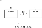
図2は、本技術を適用したワイヤレス給電システムの一実施の形態の構成例を示すブロック図である。
図2において、ワイヤレス給電システムは、送電装置11と受電装置12とを有し、例えば、磁界を利用した電磁誘導方式や磁界共鳴方式等で、ワイヤレス給電を行う。
送電装置11は、磁界を利用して、電力を送信するためのコイルである送電コイルを有し、電力を送信する。
受電装置12は、磁界を利用して、電力を受信するためのコイルである受電コイルを有し、送電装置11の近くに置かれた場合に、その送電装置11から送信される電力を受信する。
ここで、図2のワイヤレス給電システムが適用されるシステムとしては、送電装置11としての、例えば、クレードルと、受電装置12としての、例えば、携帯電話機等の携帯端末とのセットや、送電装置11としての、例えば、充電スタンドと、受電装置12としての、例えば、電気自動車とのセット、送電装置11としての、例えば、テレビラックと、受電装置12としてのTV(テレビジョン受像機)とのセット等がある。
また、図2では、1つの送電装置11から、ワイヤレス給電により電力を受信する受電装置として、1つの受電装置12だけを図示してあるが、ワイヤレス給電により電力を受信する受電装置は、複数であっても良い。
複数の受電装置を有するワイヤレス給電システムによれば、送電装置11としての、例えば、トレイ(充電トレイ)に、複数の受電装置としての、例えば、複数の携帯端末を置くことによって、その複数の携帯端末を同時に充電することができる。
[送電装置11の構成例]
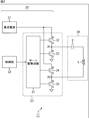
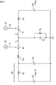
図3は、図2の送電装置11の構成例を示すブロック図である。
図3において、送電装置11は、高周波電源20、及び、共振回路24を有し、ワイヤレス給電を行う電源として機能する。
高周波電源20は、直流電源21、制御部22、及び、ドライバ回路23を有し、スイッチングにより、交流としての矩形波の電圧及び電流を出力する電源として機能する。
直流電源21は、所定の直流電圧(電流)を、ドライバ回路23に供給する。
制御部22は、ドライバ回路23(のゲート駆動回路31)や、送電装置11を構成する各ブロックを制御する。
ドライバ回路(インバータ)23は、直流電源21からの直流電圧を用いて、共振回路24をドライブし、その共振回路24を構成する送電コイルLに磁束を発生させることにより、電磁誘導方式又は磁界共鳴方式で、電力を送信させる。
共振回路24は、送電コイルL、及び、コンデンサCから構成される直列共振回路であり、ドライバ回路23によってドライブされる。共振回路24がドライブされることにより、送電コイルLに磁束(磁界)が発生し、その磁束によって、電磁誘導方式又は磁界共鳴方式で、電力が、受電装置12に送信されるワイヤレス給電が行われる。
ここで、図3では、ドライバ回路23は、フルブリッジインバータを構成しており、ゲート駆動回路31、並びに、NMOSのFET32,33,34、及び、35を有する。
ゲート駆動回路31は、制御部22の制御に従い、FET32ないし35のゲートに所定の電圧を印加することで、FET32ないし35それぞれをオン又はオフさせる(オンオフさせる)。
FET32ないし35は、パワーMOS FETであり、ゲート駆動回路31の駆動に従って、オン又はオフする(オンオフする)。
FET32のドレインは、直流電源21に接続されており、したがって、FET32のドレインには、直流電源21が出力する直流の所定の電圧が印加されている。
FET32のソースは、FET33のドレインに接続されており、FET33のソースは、接地されている(グラウンド(GND)に接続されている)。
FET34及び35は、FET32及び33と同様に接続されている。
すなわち、FET34のドレインは、直流電源21に接続され、FET34のソースは、FET35のドレインに接続されている。そして、FET35のソースは、接地されている。
さらに、FET32のソースとFET33のドレインとの接続点P1には、共振回路24の一端が接続され、FET34のソースとFET35のドレインとの接続点P2には、共振回路24の他端が接続されている。
ここで、図3において、共振回路24では、送電コイルLとコンデンサCとの一端どうしが接続されている。そして、コンデンサCの他端が、FET32のソースとFET33のドレインとの接続点P1に接続され、送電コイルLの他端が、FET34のソースとFET35のドレインとの接続点P2に接続されている。
以上のように構成されるドライバ回路23では、ゲート駆動回路31が、制御部22の制御に従い、所定のタイミングで、FET32ないし35のゲートに所定の電圧を印加することで、FET32ないし35それぞれをオン又はオフするように制御する。
これにより、FET32及び33は、それぞれ、相補的に、周期的に、オンとオフとになる。
すなわち、FET32は、周期的に、交互に、オンとオフとになる。
そして、FET32がオンになったときに、FET33はオフになり、FET32がオフになったときに、FET33はオンになる。
また、FET34及び35のセットは、FET32及び33のセットに対して相補的に、周期的に、オンとオフとになる。
すなわち、FET32がオンになり、FET33がオフになったとき、FET34はオフになり、FET35はオンになる。
さらに、FET32がオフになり、FET33がオンになったとき、FET34はオンになり、FET35はオフになる。
例えば、いま、FET32に注目すると、FET32がオンになっているとき、FET33はオフに、FET34はオフに、FET35はオンになる。
その結果、FET32のソースとFET33のドレインとの接続点P1は、直流電源21が出力する直流の所定の電圧である、例えば、H(High)レベルになり、FET34のソースとFET35のドレインとの接続点P2は、グラウンドのレベルである、例えば、L(Low)レベルになる。
したがって、共振回路24では、接続点P1から、コンデンサC及び送電コイルLを介して、接続点P2に向かう方向に、電流が流れる。
一方、FET32がオフになっているとき、FET33はオンに、FET34はオンに、FET35はオフになる。
その結果、FET34のソースとFET35のドレインとの接続点P2は、直流電源21が出力する直流の所定の電圧であるHレベルになり、FET32のソースとFET33のドレインとの接続点P1は、グラウンドのレベルであるLレベルになる。
したがって、共振回路24では、接続点P2から、送電コイルL及びコンデンサCを介して、接続点P1に向かう方向に、電流が流れる。
以上のように、共振回路24には、FET32ないし35がオン(又はオフ)になる周期の交流電圧(矩形波の電圧)が印加され、その交流電圧の印加に応じて、同様の周期の交流電流が流れる。
共振回路24に、交流電流が流れることにより、その共振回路24を構成する送電コイルLには、継続的に、磁束が発生し、その磁束によって、電力が送信される。
なお、FET32ないし35がオン(又はオフ)になる周期は、送電コイルLとコンデンサCとで構成される共振回路24の共振周期2π√(LC)、すなわち、共振回路24の共振周波数1/(2π√(LC))の逆数に設定される。
また、図3では、ドライバ回路23として、フルブリッジインバータを採用することとしたが、ドライバ回路23としては、その他、例えば、ハーフブリッジインバータ等の、FETのスイッチング(オンオフ)を行う回路を採用することができる。
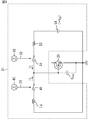
[ゲート駆動回路31の第1の構成例]
図4は、図3のゲート駆動回路31の第1の構成例を示す回路図である。
なお、図4では、図3のゲート駆動回路31のうちの、例えば、FET33を駆動する部分の構成例を図示してある。FET33以外のFET32,34,35それぞれを駆動する部分も、同様に構成される。
ゲート駆動回路31は、容量性負荷であるパワーMOS FET(のゲート)を、高効率に駆動するため、FETの駆動に用いられた電力を回生する電力回生機構を有する。
すなわち、図4において、ゲート駆動回路31は、コイル(回生用コイル)Lg、スイッチ(回生用スイッチ)41、制御部42、スイッチ(補充用スイッチ)51、制御部52、抵抗(電流制限抵抗)53、及び、直流電源54を有する。
コイルLgの一端は、スイッチ41を介して、FET33のゲートに接続されており、コイルLgの他端は、FET33のソース(図4では、グラウンドでもある)に接続されている。したがって、コイルLgは、FET33のゲートの入力容量(コンデンサ)Cissとともに(直列)共振回路を構成している。
スイッチ41(第1スイッチ)は、コイルLgの一端と、FET33のゲートとの間に設けられている。スイッチ41は、制御部42からの制御、すなわち、制御部42から供給される制御信号C1に従って、オン又はオフし、これにより、コイルLgに流れる電流i1をオン又はオフする。
ここで、本実施の形態では、コイルLgに流れる電流i1については、コイルLgから、FET33のゲートに流れる方向を、正方向とするとともに、逆方向を、負方向とする。
制御部42は、制御信号(回生用スイッチ制御信号)C1を、スイッチ41に供給することにより、スイッチ41(のオン及びオフ)を制御する。
スイッチ51(第2スイッチ)は、制御部52からの制御、すなわち、制御部52から供給される制御信号(補充用スイッチ制御信号)C2に従って、オン又はオフし、これにより、直流電源54とFET33のゲートとの接続をオン又はオフする。
すなわち、直流電源54のプラス端子は、抵抗53、及び、スイッチ51を介して、FET33のゲートに接続され、直流電源54のマイナス端子は、FET33のソースに接続されている。
したがって、スイッチ51がオン又はオフすることにより、直流電源54(のプラス端子)とFET33のゲートとの接続がオン又はオフされる。
制御部52は、制御信号C2を、スイッチ51に供給することにより、スイッチ51(のオン及びオフ)を制御する。
抵抗53は、スイッチ51がオンしたときに、直流電源54から流れる電流i2を制限するための抵抗であり、抵抗53の一端は、直流電源54のプラス端子に接続され、抵抗53の他端は、スイッチ51を介して、FET33のゲートに接続されている。
ここで、本実施の形態では、直流電源54から流れる電流(抵抗53を流れる電流)i2については、直流電源54のプラス端子から、FET33のゲートに流れる方向を、正方向とするとともに、逆方向を、負方向とする。
直流電源54は、所定の直流電圧+VDD(>0)を出力する電源である。直流電源54のプラス端子は、抵抗53、及び、スイッチ51を介して、FET33のゲートに接続され、直流電源54のマイナス端子は、FET33のソースに接続されている。したがって、スイッチ51がオンすることにより、FET33のゲートには、直流電源54の(直流)電圧+VDDが印加される。
なお、直流電源54の電圧+VDDは、FET33を駆動するのに十分な電圧(FET33がオンするときのゲートとソースとの間の電圧vgsより大の電圧)になっていることとする。
また、FET33のゲートの入力容量Cissは、等価的に、FET33のゲートとソースとの間に並列に存在する。
以上のように構成されるゲート駆動回路31では、FET33のゲートの入力容量Ciss、コイルLg、スイッチ41、及び、制御部42が、FET33の駆動に用いられた電力を回生する電力回生機構を構成している。
すなわち、例えば、いま、FET33がオンになっているとすると、FET33のゲートの入力容量Cissには、電荷が蓄積され、ゲートの電圧(ソースから見たゲートの電圧)は、Hレベルになっている。
そして、スイッチ41及び51がオフになっていることとすると、入力容量Cissに蓄積された電荷は放電されず、ゲートの電圧は、Hレベルに維持されるので、FET33もオンの状態を維持する。
なお、このときのFET33のゲートの電圧、すなわち、入力容量Cissの、ソースに接続されている端子を基準とする、ゲートに接続されている端子の電圧は、例えば、直流電源54の電圧+VDDであるとする。
スイッチ41は、制御部42の制御に従い、FET33がオフになる(スイッチングする)べきタイミングで、オンになる。
スイッチ41がオンになることにより、入力容量Cissに蓄積された電荷は、スイッチ41、及び、コイルLgを介して放電し、コイルLgには、その放電された電荷に対応する電流i1が負方向に流れる。
コイルLgに、電流i1が流れることにより、その電流i1に対応する電気エネルギ(磁気エネルギ)が、コイルLgに蓄積される。
入力容量Cissに蓄積された電荷がある程度放電され、ゲートの電圧が電圧+VDDから所定値(FET33がオンするゲートの電圧)未満に下降すると、FET33はオフになる。
そして、入力容量Cissに蓄積された電荷がすべて放電されると、コイルLgに流れる電流i1が0になろうとするが、慣性でコイルLgには、電流i1が負方向に流れ続ける。
コイルLgに、電流i1が流れ続けることにより、入力容量Cissには、電荷が蓄積され、FET33のゲートの電圧(入力容量Cissの、ソースに接続されている端子を基準とする、ゲートに接続されている端子の電圧)の極性が反転すると、すなわち、FET33のゲートの電圧が、電圧-VDDになると、コイルLgに流れる電流i1は0になる。
スイッチ41は、制御部42の制御に従い、コイルLgに流れる電流i1が0になるタイミングで、オフになる。これにより、FET33のゲートの電圧は、電圧-VDDに維持される。
その後、スイッチ41は、制御部42の制御に従い、FET33がオンになる(スイッチングする)べきタイミングで、オンになる。
スイッチ41がオンになることにより、入力容量Cissに蓄積された電荷は、コイルLg、及び、スイッチ41を介して放電し、コイルLgには、その放電された電荷に対応する電流i1が正方向に流れる。
コイルLgに、電流i1が流れることにより、その電流i1に対応する電気エネルギが、コイルLgに蓄積される。
入力容量Cissに蓄積された電荷がある程度放電され、ゲートの電圧が電圧-VDDから所定値以上に上昇すると、FET33はオンになる。
そして、入力容量Cissに蓄積された電荷がすべて放電されると、コイルLgに流れる電流i1が0になろうとするが、慣性でコイルLgには、電流i1が正方向に流れ続ける。
コイルLgに、電流i1が流れ続けることにより、入力容量Cissには、電荷が蓄積され、FET33のゲートの電圧の極性が反転すると、すなわち、FET33のゲートの電圧が、電圧+VDDになると、コイルLgに流れる電流i1は0になる。
スイッチ41は、制御部42の制御に従い、コイルLgに流れる電流i1が0になるタイミングで、オフになる。これにより、FET33のゲートの電圧は、電圧+VDDに維持される。
その後、スイッチ41は、制御部42の制御に従い、FET33がオフになるべきタイミングで、オンになり、以下、同様の動作が繰り返される。
以上のように、電力回生機構としての入力容量Ciss、コイルLg、スイッチ41、及び、制御部42では、入力容量Cissに蓄積された電気エネルギ(電荷)を、その入力容量Cissとともに共振回路を構成するコイルLgに蓄積し、コイルLgに蓄積された電気エネルギを、入力容量Cissに蓄積することを繰り返すことで、FET33の駆動に用いられた電力を回生し、その電力が、再び、FET33の駆動に用いられる。
なお、以上のような電力回生機構において、一部の電力は、熱等として損失するので、電力の回生(電力回生)を、恒久的に行うことはできない。
そのため、ゲート駆動回路31では、損失した電力が、適宜補充される。
すなわち、スイッチ51は、制御部52の制御に従って、例えば、周期的に、一時オンになる(オフからオンになる)。
スイッチ51がオンになると、電流i2が、直流電源54から、抵抗53、スイッチ51、及び、FET33のゲートを介して、入力容量Cissに流れ込み、入力容量CissとコイルLgとで構成される共振回路に、電力(電荷)が補充される。したがって、直流電源54は、電荷(電力)を補充するための電源ということができ、直流電源54から流れる電流i2は、電荷(電力)を補充するための補充電流ということができる。
[ゲート駆動回路31の第1の構成例の動作]
図5は、図4の制御部42が出力する制御信号C1、及び、制御部52が出力する制御信号C2を示す波形図である。
なお、制御信号C1及びC2は、例えば、L及びHレベルの2値をとるパルス信号である。
制御信号C1がLレベルのとき、スイッチ41はオフになり、制御信号C1がHレベルのとき、スイッチ41はオンになる。
同様に、制御信号C2がLレベルのとき、スイッチ51はオフになり、制御信号C2がHレベルのとき、スイッチ51はオンになる。
したがって、制御信号C1及びC2の波形は、それぞれ、スイッチ41及び51のオンとオフの状態をも表しており、以下、適宜、制御信号C1及びC2の波形が、それぞれ、スイッチ41及び51のオンとオフの状態を表していることとして、説明を行う。
制御部42は、図5に示すように、FET33をスイッチングする周期tCLKに対応する周期としての、例えば、周期tCLKの1/2の周期tCLK/2で、コイルLgと入力容量Cissとからなる共振回路(以下、LgCiss共振回路ともいう)の共振周期2π√(LgCiss)(LgCiss共振回路の共振周波数1/(2π√(LgCiss))の逆数)の1/2の時間tg=π√(LgCiss)だけ、(一時的に)Hレベルになり、他の期間(時間)は、Lレベルになる信号を、制御信号C1として、スイッチ41に供給する。
したがって、スイッチ41は、周期tCLK/2で、時間tgだけ、(一時的に)オンになる(他の期間(時間)はオフになる)。
制御部52は、図5に示すように、スイッチ41がオフになっている期間、すなわち、制御信号C1がLレベルになっている期間のうちの所定の期間としての時間tsだけ、周期的にHレベルになり、他の期間は、Lレベルになる信号を、制御信号C2として、スイッチ51に供給する。
したがって、スイッチ51は、スイッチ41がオフになっている期間のうちの、時間tsだけ、周期的に、(一時的に)オンになる(他の期間はオフになる)。
図6は、制御信号C2と、その制御信号C2に従ってスイッチ51が制御されることによって流れる電流(補充電流)i2とを示す波形図である。
制御信号C2がHレベルになり、スイッチ51がオンになると、直流電源54から、電流i2が流れる。
図5で説明したように、スイッチ51は、時間tsだけオンするが、スイッチ51がオンになるのは、スイッチ41がオフになっている期間であるから、直流電源54から流れる電流i2(電荷)は、抵抗53、及び、オンになっているスイッチ51を介して、FET33のゲートの入力容量Cissに流れ込む。
したがって、スイッチ51がオンになった瞬間は、直流電源54から流れる電流i2によって、FET33のゲートの入力容量Cissに、電荷が、瞬時的に蓄積され、その後、入力容量Cissに蓄積される電荷は、急激に減少していく。
その結果、図6に示すように、電流i2としては、スイッチ51がオンになった瞬間、瞬時的に、大きな電流が流れ、その後、電流i2は、急激に減少していく。電流i2が減少していく速度(時間)は、抵抗53と入力容量Cissとから求められる時定数によって決まる。
図5及び図6では、スイッチ41がオンになる周期の2周期に1回の割合で、スイッチ51がオンになり、入力容量CissとコイルLgとで構成されるLgCiss共振回路の入力容量Cissに、電荷が蓄積(補充)される。
ここで、スイッチ51がオンになる割合は、スイッチ41がオンになる周期の2周期に1回の割合に限定されるものではない。
図7は、制御信号C1、制御信号C1に従ってスイッチ41が制御されることによって流れる電流(回生電流)i1、及び、ゲート電圧(FET33のゲートの電圧)を示す波形図である。
なお、図7では、制御信号C1(スイッチ41のオンとオフ)、電流i1、及び、ゲート電圧の他、参考として、図6に示した制御信号C2(スイッチ52のオンとオフ)も、図示してある。
図5で説明したように、スイッチ41(制御信号C1)は、周期tCLK/2で、時間tgだけ、オンになる。
ここで、図5で説明したように、スイッチ51がオンになるのは、スイッチ41がオフになっている期間であるから、スイッチ41がオンになっている時間tgでは、スイッチ51はオフになっている。
したがって、スイッチ41がオンした場合には、そのオンになっているスイッチ41を介して、入力容量CissとコイルLgとで構成されるLgCiss共振回路だけが導通状態となる(抵抗53や直流電源54と、コイルLgや入力容量Cissとは、導通状態にはならない)。
例えば、いま、ゲート電圧が正の電圧+VDDになるように、電荷が、入力容量Cissに蓄積されているとすると、スイッチ41がオンした場合には、入力容量Cissに蓄積されている電荷が、入力容量Cissから、スイッチ41、コイルLgの順番で流れることよって、電流i1は、図7に示すように、LgCiss共振回路を、負方向に流れる。
負方向の電流i1は、スイッチ41がオンしている時間tgだけ流れ、これにより、ゲート電圧が負の電圧-VDDに(ほぼ)なるように、電荷が、入力容量Cissに蓄積される。
その後、スイッチ41が、再び、時間tgだけ、オンになると、ゲート電圧が負の電圧-VDDになるように、入力容量Cissに蓄積されている電荷が、入力容量Cissから、コイルLg、スイッチ41の順番で流れることよって、電流i1は、図7に示すように、LgCiss共振回路を、正方向に流れる。
正方向の電流i1は、スイッチ41がオンしている時間tgだけ流れ、これにより、ゲート電圧が正の電圧+VDDに(ほぼ)なるように、電荷が、入力容量Cissに蓄積される。
以下、同様に、スイッチ41が、周期tCLK/2で、オンするたびに、入力容量Cissに蓄積された電荷によって、電流i1が、LgCiss共振回路を、正方向に流れることと、負方向に流れることとが、交互に繰り返される。
その結果、ゲート電圧は、時間tCLK/2ごとに、交互に、正の電圧+VDD(Hレベル)と負の電圧-VDD(Lレベル)になり、FET33は、周期tCLKでスイッチングされる。
すなわち、図7において、FET33は、周期tCLKで、時間tCLK/2だけ、(一時的に)オンになる(その後の、時間tCLK/2はオフになる)。
なお、図7では、ゲート電圧は、正の電圧+VDDになっている時間と、負の電圧-VDDになっている時間とがいずれも時間tCLK/2で、同一になっている、デューティ比が50%のパルスになる。
スイッチ41が周期tCLK/2でオンする、連続する2つのタイミング(オンタイミング)のセットについて、その2つのオンタイミングのセットのうちの一方のタイミングをずらすことにより、ゲート電圧のデューティ比を調整することができる。
すなわち、例えば、いま、あるオンタイミングのセットの1番目のオンタイミングで、ゲート電圧が正の電圧+VDDになったとすると、その1番目のオンタイミングから2番目のオンタイミングまでの期間が、ゲート電圧が正の電圧+VDDになる期間であり、2番目のオンタイミングから、次のオンタイミングのセットの1番目のオンタイミングまでの期間が、ゲート電圧が負の電圧-VDDになる期間になる。
したがって、オンタイミングのセットのうちの、例えば、2番目のオンタイミングをずらすことにより、ゲート電圧が正の電圧+VDDになる期間と、負の電圧-VDDになる期間とを調整すること、すなわち、ゲート電圧のデューティ比を調整することができる。
なお、本実施の形態では、図5及び図6で説明したように、スイッチ41がオンになる周期の2周期に1回の割合で、スイッチ51がオンになり、入力容量CissとコイルLgとで構成されるLgCiss共振回路の入力容量Cissに、電荷が補充される。
本実施の形態では、FET33のゲートに、直流電源54のプラス端子が(抵抗53、及び、スイッチ51を介して)接続され、正の電圧+VDDが印加されるため、その正の電圧+VDDが印加されるゲートの入力容量Cissへの電荷の補充、すなわち、スイッチ51(制御信号C2)をオンにすることは、図7に示すように、ゲート電圧が正の電圧+VDD(Hレベル)になっているタイミングで行われる。
ゲートの入力容量Cissへの電荷の補充を、ゲート電圧が負の電圧-VDD(Lレベル)になっているタイミングで行う場合には、そのタイミングにおいて、FET33のゲートには、直流電源54のマイナス端子を(抵抗53、及び、スイッチ51を介して)接続し、負の電圧-VDD(Lレベル)を印加する。
図8は、電流i1とゲート電圧との関係を説明する図である。
例えば、いま、ゲート電圧が正の電圧+VDDになるように、電荷(電気エネルギ)が、入力容量Cissに蓄積されているとする。
この場合に、スイッチ41がオンすると、入力容量Cissに蓄積されている電荷が、入力容量Cissから、スイッチ41、コイルLgの順番で流れる(放電される)ことよって、LgCiss共振回路の共振周期2π√(LgCiss)の正弦波で表される電流i1が、コイルLgに、負方向に流れる(期間T1)。
入力容量Cissからの電荷の放電(入力容量Cissに蓄積されている電荷が、入力容量Cissから、スイッチ41、コイルLgの順番で流れていくこと)によって、ゲート電圧は、正の電圧+VDDから低下し、入力容量Cissに蓄積されている電荷がすべて放電されると(スイッチ41がオンされてから、LgCiss共振回路の共振周期2π√(LgCiss)の1/4周期である時間tg/2が経過したとき)、ゲート電圧は、0Vになる(期間T1)。
このとき、コイルLgに蓄えられる電気エネルギは、最大になる。
入力容量Cissに蓄積されている電荷がすべて放電されると、コイルLgに流れる電流i1が0Aになろうとするが、慣性で、すなわち、コイルLgに蓄えられた電気エネルギにより、コイルLgには、電流i1が負方向に流れ続ける(期間T2)。
コイルLgに、電流i1が流れ続けることにより、入力容量Cissには、ゲート電圧が負の電圧になるように、電荷が蓄積(充電)される(期間T2)。
そして、スイッチ41がオンされた最新のタイミングから、LgCiss共振回路の共振周期2π√(LgCiss)の1/2周期tgが経過したとき、コイルLgに蓄えられる電気エネルギは0になり、コイルLgに流れる電流i1は0Aになる(タイミングT3)。
このとき、入力容量Cissには、ゲート電圧が負の電圧-VDDになるように、電荷が蓄積されており、スイッチ41がオフにされることにより、LgCiss共振回路はオープンになり、ゲート電圧は、負の電圧-VDDに固定される(タイミングT3)。
スイッチ41は、前回、オンにされてから、FET33をスイッチングする周期tCLKの1/2の周期tCLK/2が経過したときに、再び、オンにされる。
スイッチ41がオンになると、入力容量Cissに蓄積されている電荷が、入力容量Cissから、コイルLg、スイッチ41の順番で流れる(放電される)ことよって、LgCiss共振回路の共振周期2π√(LgCiss)の正弦波で表される電流i1が、コイルLgに、正方向に流れる(期間T4)。
入力容量Cissからの電荷の放電(入力容量Cissに蓄積されている電荷が、入力容量Cissから、コイルLgスイッチ41の順番で流れていくこと)によって、ゲート電圧は、負の電圧-VDDから上昇し、入力容量Cissに蓄積されている電荷がすべて放電されると(スイッチ41がオンされてから、LgCiss共振回路の共振周期2π√(LgCiss)の1/4周期である時間tg/2が経過したとき)、ゲート電圧は、0Vになる(期間T4)。
このとき、コイルLgに蓄えられる電気エネルギは、再び、最大になる。
入力容量Cissに蓄積されている電荷がすべて放電されると、コイルLgに流れる電流i1が0Aになろうとするが、慣性でコイルLgには、電流i1が正方向に流れ続ける(期間T5)。
コイルLgに、電流i1が流れ続けることにより、入力容量Cissには、ゲート電圧が正の電圧になるように、電荷が蓄積(充電)される(期間T5)。
そして、スイッチ41がオンされた最新のタイミングから、LgCiss共振回路の共振周期2π√(LgCiss)の1/2周期tgが経過したとき、コイルLgに蓄えられる電気エネルギは0になり、コイルLgに流れる電流i1は0Aになる(タイミングT6)。
このとき、入力容量Cissには、ゲート電圧が正の電圧+VDDになるように、電荷が蓄積されており、スイッチ41がオフにされることにより、LgCiss共振回路はオープンになり、ゲート電圧は、正の電圧+VDDに固定される(タイミングT3)。
スイッチ41は、前回、オンにされてから、FET33をスイッチングする周期tCLKの1/2の周期tCLK/2が経過したときに、再び、オンにされ、以下、同様の処理が繰り返される。
以上のように、ゲート駆動回路31では、入力容量Cissに蓄積された電気エネルギ(電荷)を、その入力容量CissとともにLgCiss共振回路を構成するコイルLgに蓄積し、コイルLgに蓄積された電気エネルギを、入力容量Cissに蓄積することを繰り返すことで、FET33の駆動に用いられた電力を電力回生し、その電力が、再び、FET33の駆動に用いられる。
なお、以上のような電力回生において、一部の電力は、熱等として損失する。そのため、スイッチ51が周期的にオンにされることによって、直流電源54の電圧+VDDが、抵抗53、及び、スイッチ51を介して、FET33のゲートの入力容量Cissに印加されることによって、LgCiss共振回路の入力容量Cissに、電力(電荷)が補充される。
図9は、ゲート駆動回路31の電力回生と、力学としてのバネの振動(運動)との対応を説明する図である。
図9に示すように、天井に、バネ(つるまきバネ)の一端を固定するとともに、バネの他端に、重りをつけ、手で、バネを伸ばすか、縮ませてから、手を離すと、バネは、上下(重力と平行な方向)に伸縮し、バネの他端につけられた重りは、バネの伸縮に伴って上下に振動(移動)する。
この場合、重りの力学的エネルギは、式kx2/2+mv2/2で表される。
ここで、kは、バネ定数を表し、xは、天井に一端を固定したバネの他端に、重りをつけて、重りが振動しないように、手を離したときの重りの位置を基準位置とする、重りの位置(変位量)を表す。
また、mは、重りの質量を表し、vは、重りの速度を表す。
基準位置に対して、バネの縮みが最大のときと、バネの伸びが最大のときとに、すなわち、変位量xが最大のときと最小のときとに、重りの速度vは0になる。
また、バネの伸縮が0のときに、すなわち、変位量xが0のときに、重りの速度(速さ)vは、最大になる。
一方、LgCiss共振回路の電気的エネルギは、式CV2/2+LI2/2で表される。
ここで、Cは、入力容量(静電容量)Cissを表し、Vは、入力容量Cissにかかる電圧、すなわち、本実施の形態では、ゲート電圧を表す。
また、Lは、コイル(のインダクタンス)Lgを表し、Iは、コイルLgに流れる電流i1を表す。
ゲート電圧が、正側に最大のときと、負側に最大のときとに、すなわち、ゲート電圧が最大のときと最小のときとに、LgCiss共振回路のコイルLgに流れる電流I=i1は0になる。
また、ゲート電圧が0であるときに、コイルLgに流れる電流I=i1は、最大になる。
以上のような重りの力学的エネルギと、LgCiss共振回路の電気的エネルギとでは、例えば、バネの縮みが最大のときと、ゲート電圧が正側に最大のときとが対応するとともに、バネの伸びが最大のときと、ゲート電圧が負側に最大のときとが対応する。さらに、重りの速度vが0のときと、コイルLgに流れる電流I=i1が0のときとが対応する。
また、重りの力学的エネルギと、LgCiss共振回路の電気的エネルギとでは、例えば、バネの伸縮が0のときと、ゲート電圧が0のときとが対応する。さらに、重りの速度(速さ)vが最大のときと、コイルLgに流れる電流I=i1が最大のときとが対応する。
図10は、電流i1及びi2を示す波形図である。
図5ないし図8で説明したように、スイッチ41が、時間tgだけオンになり、その時間tgだけ、LgCiss共振回路に電流i1が流れることによって、FET33のゲート電圧の極性が反転する(Hレベル及びLレベルのうちの一方から他方になる)。
したがって、ゲート電圧の極性の反転に必要な電荷の量は、時間tgの間に、LgCiss共振回路に流れる電流i1を積分した値である。
一方、ゲート駆動回路31において、外部から電気的エネルギの供給を受けずに、電気的エネルギを他に供給することができるのは、直流電源54だけであり、その直流電源54が他に供給する電気的エネルギは、LgCiss共振回路の入力容量Cissに、電力(電荷)を補充するための電流(補充電流)i2だけである。
電流i2は、熱等として失われた電力を補充するための補充電流であるため、図10に示すように、電流i1に比較して極めて小さい。
電力回生機構を有する図4のゲート駆動回路31によれば、FET33の駆動(スイッチング)に必要な電流量を、LgCiss共振回路に流れる電流i1の量から、その電流i1に比較して極めて小さい電流i2の量に改善することができる。
すなわち、FET33をオンするときには、大きな入力容量Cissを充電するために、大きな電流i1が必要であり、電力回生を行わない場合には、FET33をオフするときに、FET33をオンするときに用いた大きな電流i1(に対応する電荷)がすべて捨てられるが、電力回生機構を有するゲート駆動回路31では、電流i1が、電力回生によって再利用され、その電力回生において熱等として失われた電力が、大きな電流i1に比較して極めて小さい電流i2で補充される。
したがって、ゲート駆動回路31によれば、FET33をスイッチングする際の電力(電荷)の損失を、大きな電流i1に相当する電力から、小さな電流i2に相当する電力に、大きく低減することができる。
図11は、図5ないし図8、及び、図10の波形図を求めるシミュレーションに用いた回路(シミュレーション用回路)を示す回路図である。
シミュレーション用回路は、図4のFET33に代えて、そのFET33のゲートの代わりとなるコンデンサCGと抵抗RGとの並列回路が設けられている点を除き、図4に示した回路と同様に構成されている。
図11のシミュレーション用回路において、コンデンサCGは、FET33のゲートの入力容量Cissに相当し、抵抗RGは、FET33のゲートの入力抵抗に相当する。
なお、FET33のゲートの入力抵抗としての抵抗RGは、非常に大きな抵抗値の抵抗であるため、シミュレーション用回路において、そのような大きな抵抗RGは、なくてもよい(省略することができる)。
以上のように、図4のゲート駆動回路31では、コイルLg、スイッチ41、制御部42、スイッチ51、制御部52、抵抗53、及び、直流電源54という簡単な回路構成で、FETをスイッチングする際の電力(電荷)の損失を低減することができる。
[ゲート駆動回路31の第2の構成例]
図12は、図3のゲート駆動回路31の第2の構成例を示す回路図である。
なお、図中、図4の第1の構成例と対応する部分については、同一の符号を付してあり、以下では、その説明は、適宜省略する。
すなわち、図12のゲート駆動回路31は、コイルLg、スイッチ41、制御部42、スイッチ51、制御部52、抵抗53、及び、直流電源54を有する点で、図4の第1の構成例と共通する。
但し、図12のゲート駆動回路31は、(直流電圧)オフセット回路60が新たに設けられている点で、図4の第1の構成例と相違する。
オフセット回路60は、直流電源61、抵抗(バイアス抵抗)62、及び、コンデンサ(バイパスコンデンサ)63を有し、FET33のゲート電圧を、所定値以上の電圧にオフセットする。
ここで、図4の第1の構成例では、図7及び図8で説明したように、FET33のゲート電圧は、直流電源54の電圧である電圧+VDDから、その電圧+VDDの符号を逆にした電圧-VDDまでの範囲の電圧になる。
NMOSのFETのゲートに対して、負の電圧が印加されることは予定されていないことがあり、負の電圧-VDDが、FETの性能を保証する性能保証電圧未満である場合には、ゲート駆動回路31の信頼性を損ねることがあり得る。
そこで、図12のゲート駆動回路31では、オフセット回路60によって、FET33のゲート電圧が、所定値としての、例えば、0V以上の電圧にオフセットされる。
ここで、図12のゲート駆動回路31では、ゲート電圧が、直流電源54の電圧である電圧+VDDから0Vまでの範囲の電圧になるように、オフセットされる。
すなわち、直流電源61は、直流電源54が出力する直流電圧+VDDの、例えば、1/2の直流電圧+VDD/2を出力する電源である。直流電源61のプラス端子は、抵抗62の一端に接続されており、直流電源61のマイナス端子は、コンデンサ63の一端に接続されている。
抵抗62は、コイルLgの、スイッチ41と接続されていない方の一端、ひいては、FET33のゲートをバイアスするための抵抗である。抵抗62の一端は、上述したように、直流電源61のプラス端子に接続されており、抵抗62の他端は、コンデンサ63の他端に接続されている。
コンデンサ63は、LgCiss共振回路に流れる電流をバイパスするためのコンデンサである。上述したように、コンデンサ63の一端は、直流電源61のマイナス端子に接続されており、コンデンサ63の他端は、抵抗62の他端と接続されている。
そして、以上のように構成されるオフセット回路60の抵抗62とコンデンサ63との接続点が、コイルLgの、スイッチ41と接続されていない方の一端(一端がスイッチ41を介してFET44のゲートと接続されているコイルLgの他端)に接続され、直流電源61とコンデンサ63との接続点が、FET33のソース(図12では、グラウンドでもある)に接続されている。
図12のLgCiss共振回路において、電流i1は、コンデンサ63を介して(バイパスして)、図4の場合と同様のタイミングで流れる。
但し、オフセット回路60において、コイルLgの、スイッチ41と接続されていない方の一端は、0V(グラウンドレベル)ではなく、直流電源61の電圧+VDD/2にバイアスされ、コイルLgに印加される電圧は、+VDDから+VDD/2になる。
その結果、コイルLgに流れる電流i1は、図4の場合の1/2になり、さらに、FET33のゲートが、図4の場合から、電圧+VDD/2だけバイアスされるので、FET33のゲート電圧は、図4の場合のゲート電圧の範囲を1/2にして、電圧+VDD/2だけバイアスした範囲、すなわち、電圧+VDDから0Vまでの範囲になる。
[ゲート駆動回路31の第2の構成例の動作]
図13は、図12のゲート駆動回路31についての、スイッチ51のオンとオフの状態(制御信号C2)、スイッチ51がオンオフされることによって流れる電流i2、スイッチ41のオンとオフの状態(制御信号C1)、スイッチ41がオンオフされることによって流れる電流i1、及び、ゲート電圧を示す波形図である。
スイッチ51のオンとオフの状態(制御信号C2)、スイッチ51がオンオフされることによって流れる電流i2、及び、スイッチ41のオンとオフの状態(制御信号C1)は、オフセット回路60が設けられている場合であっても、オフセット回路60がない図5ないし図8で説明した場合と同一になる。
スイッチ41がオンオフされることによって流れる電流i1は、図13に示すように、図5ないし図8で説明した場合の1/2の大きさになる。
すなわち、オフセット回路60によれば、コイルLgの、スイッチ41と接続されていない方の一端が、直流電源61の電圧+VDD/2にバイアスされる。
ここで、例えば、ゲート電圧が電圧+VDDである場合、図4のゲート駆動回路31では、コイルLgの、スイッチ41と接続されていない方の一端が、グラウンドに接続されているため、コイルLgの両端の電位差は、電圧+VDD(=+VDD-0)となる。
一方、図12のゲート駆動回路31では、コイルLgの、スイッチ41と接続されていない方の一端が、電圧+VDD/2にバイアスされているため、例えば、ゲート電圧が電圧+VDDである場合には、コイルLgの両端の電位差は、電圧+VDD/2(=+VDD-VDD/2)となる。
その結果、図12のゲート駆動回路31では、コイルLg、ひいては、LgCiss共振回路に流れる電流i1は、図4の場合の1/2になり、ゲート電圧の範囲も、図4の場合の電圧-VDDから電圧+VDDまでの範囲の1/2の範囲になる。
さらに、図12のゲート駆動回路31では、コイルLgの、スイッチ41と接続されていない方の一端が、電圧+VDD/2にバイアスされているため、ゲート電圧も、その電圧+VDD/2だけバイアスされ、結局、ゲート電圧の範囲は、図13に示すように、図4の場合の電圧-VDDから電圧+VDDまでの範囲の1/2の範囲を、電圧+VDD/2だけバイアスした、0Vから電圧+VDDまでの範囲となる。
図14は、図13の波形図を求めるシミュレーションに用いた回路(シミュレーション用回路)を示す回路図である。
シミュレーション用回路は、図12のFET33に代えて、そのFET33のゲートの代わりとなるコンデンサCGと抵抗RGとの並列回路が設けられている点を除き、図12に示した回路と同様に構成されている。
図11で説明したように、コンデンサCGは、FET33のゲートの入力容量Cissに相当し、抵抗RGは、FET33のゲートの入力抵抗に相当する。また、シミュレーション用回路において、抵抗RGは、なくてもよい。
[ゲート駆動回路31の第3の構成例]
図15は、図3のゲート駆動回路31の第3の構成例を示す回路図である。
なお、図中、図12の第2の構成例と対応する部分については、同一の符号を付してあり、以下では、その説明は、適宜省略する。
図15のゲート駆動回路31は、コイルLg、スイッチ41、スイッチ51、制御部52、抵抗53、直流電源54、及び、オフセット回路60を有する点で、図12の第2の構成例と共通する。
但し、図15のゲート駆動回路31は、電流検出部71が新たに設けられているとともに、制御部42に代えて、制御部72が設けられている点で、図12の第2の構成例と相違する。
ここで、FET33の入力容量(静電容量)Cissや、コイルLgのインダクタンスは、ばらつくことがある。入力容量Cissや、コイルLgのインダクタンスがばらつくと、LgCiss共振回路の共振周期2π√(LgCiss)=2×tgが変化するため、スイッチ41をオンしている時間tg、より具体的には、スイッチ41をオンした後にオフすべきタイミングも変化する。
LgCiss共振回路の共振周期2π√(LgCiss)の変化を防止する方法としては、例えば、FET33のゲート(の入力容量Ciss)と並列に、トリマコンデンサを設け、図3のドライバ回路23ごとに(個体別に)、LgCiss共振回路の共振周期が、あらかじめ想定した入力容量CissとコイルLgとで決まる共振周期2π√(LgCiss)に一致するように、トリマコンデンサを調整する方法がある。
但し、トリマコンデンサを設けて、LgCiss共振回路の共振周期2π√(LgCiss)の変化を防止する方法は、トリマコンデンサの調整等の手間や、トリマコンデンサを設けるコスト、実装面積等の面で、有利であるとは、言い難い。
そこで、図15のゲート駆動回路31は、スイッチ41の切り換え(オンとオフ)を適応的に制御することで、トリマコンデンサを設けずに、LgCiss共振回路の共振周期2π√(LgCiss)の変化に対処する。
したがって、図15のゲート駆動回路31によれば、トリマコンデンサを設ける場合に必要となる手間や、コスト、実装面積等が不要である点で、有利である。
図15において、電流検出部71は、コイルLgに流れる電流i1(の電流値)を検出し、制御部72に供給する。
制御部72は、図4の制御部42と同様に、制御信号C1を、スイッチ41に供給することにより、スイッチ41(のオン及びオフ)を制御する。
但し、制御部72は、FET33をスイッチングする周期tCLKに対応する周期としての、例えば、周期tCLKの1/2の周期tCLK/2でオンし、その後、電流検出部71から供給される電流i1に応じてオフするように、スイッチ41を制御する。
[ゲート駆動回路31の第3の構成例の動作]
図16は、図15のゲート駆動回路31についての、スイッチ51のオンとオフの状態(制御信号C2)、スイッチ51がオンオフされることによって流れる電流i2、スイッチ41のオンとオフの状態(制御信号C1)、スイッチ41がオンオフされることによって流れる電流i1、及び、ゲート電圧を示す波形図である。
スイッチ51のオンとオフの状態(制御信号C2)、及び、スイッチ51がオンオフされることによって流れる電流i2は、図5ないし図8で説明した場合と同一になる。
また、スイッチ41(制御信号C1)は、図5で説明したように、周期tCLK/2で、オンになる。
ここで、図5では、スイッチ41は、周期tCLK/2で、時間tg=π√(LgCiss)だけオンになるが、すなわち、スイッチ41は、周期tCLK/2で、オンになり、オンになってから、時間tg=π√(LgCiss)の経過後にオフになるが、図15のゲート駆動回路31では、制御部72が、電流検出部71で検出される電流i1に基づき、適応的に、スイッチ41をオフにする。
制御部72の制御により、スイッチ41は、オンになってから、電流i1の大きさ(絶対値|i1|)が所定の閾値(以下)になると、オフになる。
その結果、電流i1は、図16に示すように流れる。
すなわち、例えば、いま、ゲート電圧が電圧+VDDになるように、電荷が、入力容量Cissに蓄積されており、時刻t11において、スイッチ41がオンしたとすると、入力容量Cissに蓄積されている電荷が、入力容量Cissから、スイッチ41、コイルLgの順番で流れる(放電される)ことよって、LgCiss共振回路の共振周期2π√(LgCiss)の正弦波で表される電流i1が、コイルLgに、負方向に流れる。
電流i1が負方向に流れることによって、ゲート電圧は、電圧+VDDから低下する。
そして、入力容量Cissに蓄積されている電荷がすべて放電されると、ゲート電圧は、オフセット回路60でバイアスされる電圧(バイアス電圧)+VDD/2になる。また、コイルLgに流れる電流i1は0Aになろうとするが、慣性でコイルLgには、電流i1が流れ続ける。
コイルLgに、電流i1が流れ続けることにより、入力容量Cissには、ゲート電圧が、バイアス電圧+VDD/2より低い電圧になるように、電荷が蓄積(充電)される。
ここで、理論的には、スイッチ41がオンし、電流i1が流れ始めた直前の時刻t11から、LgCiss共振回路の共振周期2π√(LgCiss)の1/2の時間が経過したときに、コイルLgに流れる電流i1は、0Aになる。
したがって、所定の閾値として、0を設定すれば、電流i1が、所定の閾値である0になったタイミングが、電流i1が流れ始めた直前の時刻t11から、LgCiss共振回路の共振周期2π√(LgCiss)の1/2の時間が経過したタイミングとなる。
そして、電流i1が流れ始めた直前の時刻t11から、LgCiss共振回路の共振周期2π√(LgCiss)の1/2の時間が経過したタイミングでは、入力容量Cissには、ゲート電圧が、バイアス電圧+VDD/2より電圧VDD/2だけ低い0Vになるように、電荷が蓄積されている(はずな)ので、そのタイミングで、スイッチ41をオフにし、ゲート電圧を0Vに固定するのが、理想的である。
しかしながら、実際の回路では、電流i1が、所定の閾値である0になったことが検出されてから、スイッチ41をオフする等の動作を開始すると、タイミングが遅れる等の問題がある。
そこで、本実施の形態では、0Aからマージンをとった値、すなわち、0Aに近い小さい正の値TH11から得られる正の値+TH11と負の値-TH11とを、電流i1の所定の閾値として設定し、制御部72は、電流i1が、閾値+TH11又は-TH11になったときに、電流i1が流れ始めてから、LgCiss共振回路の共振周期2π√(LgCiss)の1/2の時間が経過したとして、スイッチ41をオフに制御する。
図16では、慣性でコイルLgに流れ続ける電流i1が、時刻t12において、閾値-TH11になっており、その時刻t12で、スイッチ41がオフにされる。
このとき、入力容量Cissには、ゲート電圧が(ほぼ)0Vになるように、電荷が蓄積されており、スイッチ41がオフにされることにより、LgCiss共振回路はオープンになって、ゲート電圧は、図16に示すように、0Vに固定される。
スイッチ41は、前回、オンにされた時刻t11から、FET33をスイッチングする周期tCLKの1/2の周期tCLK/2が経過した時刻t13に、再び、オンにされる。
スイッチ41がオンになると、コンデンサ63に蓄積されている電荷が、コイルLg、スイッチ41、入力容量Cissの順番で流れる(充電される)ことよって、LgCiss共振回路の共振周期2π√(LgCiss)の正弦波で表される電流i1が、コイルLgに、正方向に流れる。
電流i1が正方向に流れることによって、ゲート電圧は、0Vから上昇する。
やがて、ゲート電圧は、バイアス電圧+VDD/2に到達し、コイルLgに流れる電流i1は0Aになろうとするが、慣性でコイルLgには、電流i1が流れ続ける。
コイルLgに、電流i1が流れ続けることにより、入力容量Cissには、ゲート電圧が、バイアス電圧+VDD/2より高い電圧になるように、電荷が蓄積(充電)される。
そして、制御部72は、電流i1が、閾値+TH11又は-TH11になったときに、電流i1が流れ始めてから、LgCiss共振回路の共振周期2π√(LgCiss)の1/2の時間が経過したとして、スイッチ41をオフに制御する。
図16では、時刻t13で、スイッチ41がオンにされた後に、慣性でコイルLgに流れ続ける電流i1が、時刻t14において、閾値+TH11になっており、その時刻t14で、スイッチ41がオフにされる。
このとき、入力容量Cissには、ゲート電圧が(ほぼ)+VDDになるように、電荷が蓄積されており、スイッチ41がオフにされることにより、LgCiss共振回路はオープンになって、ゲート電圧は、図16に示すように、+VDDに固定される。
スイッチ41は、前回、オンにされた時刻t13から、FET33をスイッチングする周期tCLKの1/2の周期tCLK/2が経過した時刻t15に、再び、オンにされ、以下、同様の処理が繰り返される。
図17は、図15の制御部72によるスイッチ41の制御を説明するフローチャートである。
ステップS11において、制御部72は、スイッチ41をオンにして、処理は、ステップS12に進む。
ステップS12では、制御部72は、電流検出部71により検出される電流i1の大きさ(絶対値)|i1|が、閾値TH11より大(以上)になったかどうかを判定する。
ステップS12において、電流i1の大きさ|i1|が、閾値TH11より大になっていないと判定された場合、処理は、ステップS12に戻る。
また、ステップS12において、電流i1の大きさ|i1|が、閾値TH11より大になったと判定された場合、処理は、ステップS13に進み、制御部72は、電流検出部71により検出される電流i1の大きさ|i1|が、閾値TH11以下になったかどうかを判定する。
ステップS13において、電流i1の大きさ|i1|が、閾値TH11以下になっていないと判定された場合、処理は、ステップS13に戻る。
また、ステップS13において、電流i1の大きさ|i1|が、閾値TH11以下になったと判定された場合、処理は、ステップS14に進み、制御部72は、電流i1が流れ始めてから、LgCiss共振回路の共振周期2π√(LgCiss)の1/2の時間が経過したとして、スイッチ41をオフにして、処理は、ステップS15に進む。
ここで、図16に示したように、スイッチ41がオンにされるときには、コイルLgに流れる電流i1は0Aであり、スイッチ41がオンになると、電流i1は、0Aから上昇し、その後、再び、0Aに向かって下降する。
したがって、スイッチ41がオンにされた後、電流i1の大きさ|i1|は、0Aから閾値TH11を超えて上昇し、その後、閾値TH11以下に下降する。
スイッチ41をオフにするべきタイミングは、電流i1の大きさ|i1|が下降して、閾値TH11になったときであるので、図17では、ステップS12において、電流i1の大きさ|i1|が、閾値TH11より大になったと判定され、電流i1の大きさ|i1|が0Aから閾値TH11を超えて上昇したことが確認された後に、ステップS13において、電流i1の大きさ|i1|が、閾値TH11以下になったかどうか、すなわち、スイッチ41をオフにするべきタイミングであるかどうかが判定される。
ステップS15では、制御部72は、前回のスイッチ41のオン(のタイミング)から、時間tCLK/2が経過したかどうかを判定する。
ステップS15において、前回のスイッチ41のオンから、時間tCLK/2が、まだ経過していないと判定された場合、処理は、ステップS15に戻る。
また、ステップS15において、前回のスイッチ41のオンから、時間tCLK/2が経過したと判定された場合、処理は、ステップS11に戻り、制御部72は、スイッチ41をオンにし、以下、同様の処理が繰り返される。
[ゲート駆動回路31の第4の構成例]
図18は、図3のゲート駆動回路31の第4の構成例を示す回路図である。
なお、図中、図15の第3の構成例と対応する部分については、同一の符号を付してあり、以下では、その説明は、適宜省略する。
図18のゲート駆動回路31は、コイルLg、スイッチ41、スイッチ51、制御部52、抵抗53、直流電源54、オフセット回路60、電流検出部71、及び、制御部72を有する点で、図15の第3の構成例と共通する。
但し、図18のゲート駆動回路31は、コイル73を有し、電流検出部71がコイル73に流れる電流に基づき、コイルLgに流れる電流i1(の電流値)を検出する点で、図15の第3の構成例と相違する。
図18のゲート駆動回路31も、図15のゲート駆動回路31と同様に、スイッチ41の切り換えを適応的に制御することで、トリマコンデンサを設けずに、LgCiss共振回路の共振周期2π√(LgCiss)の変化に対処する。
すなわち、コイル73は、コイルLgの近傍に設けられており、したがって、コイル73には、電磁誘導により、コイルLgに流れる電流i1に比例する電流が流れる。
電流検出部71は、コイル73に流れる電流を検出し、その電流に基づき、コイルLgに流れる電流i1(の電流値)を検出して、制御部72に供給する。
制御部72は、制御信号C1を、スイッチ41に供給することにより、図15ないし図17で説明した場合と同様に、スイッチ41(のオン及びオフ)を制御する。
[ゲート駆動回路31の第5の構成例]
図19は、図3のゲート駆動回路31の第5の構成例を示す回路図である。
なお、図中、図12の第2の構成例と対応する部分については、同一の符号を付してあり、以下では、その説明は、適宜省略する。
図19のゲート駆動回路31は、コイルLg、スイッチ41、スイッチ51、制御部52、抵抗53、直流電源54、及び、オフセット回路60を有する点で、図12の第2の構成例と共通する。
但し、図19のゲート駆動回路31は、電圧検出部81が新たに設けられているとともに、制御部42に代えて、制御部82が設けられている点で、図12の第2の構成例と相違する。
電圧検出部81は、ゲート電圧(値)を検出し、制御部82に供給する。
制御部82は、図4の制御部42と同様に、制御信号C1を、スイッチ41に供給することにより、スイッチ41(のオン及びオフ)を制御する。
但し、制御部82は、FET33をスイッチングする周期tCLKに対応する周期としての、例えば、周期tCLKの1/2の周期tCLK/2でオンし、その後、電圧検出部81から供給されるゲート電圧に応じてオフするように、スイッチ41を制御する。
[ゲート駆動回路31の第5の構成例の動作]
図20は、図19のゲート駆動回路31についての、スイッチ51のオンとオフの状態(制御信号C2)、スイッチ51がオンオフされることによって流れる電流i2、スイッチ41のオンとオフの状態(制御信号C1)、スイッチ41がオンオフされることによって流れる電流i1、及び、ゲート電圧を示す波形図である。
スイッチ51のオンとオフの状態(制御信号C2)、及び、スイッチ51がオンオフされることによって流れる電流i2は、図5ないし図8で説明した場合と同一になる。
また、スイッチ41(制御信号C1)は、図5で説明したように、周期tCLK/2で、オンになる。
ここで、図5では、スイッチ41は、周期tCLK/2で、オンになり、オンになってから、時間tg=π√(LgCiss)の経過後にオフになるが、図19のゲート駆動回路31では、制御部82が、電圧検出部81で検出されるゲート電圧に基づき、適応的に、スイッチ41をオフにする。
制御部82の制御により、スイッチ41は、オンになってから、ゲート電圧が所定の閾値としての第1の閾値TH21(以下)、又は、第1の閾値TH21より大の第2の閾値TH22(以上)になると、オフになる。
その結果、電流i1は、図20に示すように流れる。
すなわち、例えば、いま、ゲート電圧が電圧+VDDになるように、電荷が、入力容量Cissに蓄積されており、時刻t21において、スイッチ41がオンしたとすると、入力容量Cissに蓄積されている電荷が、入力容量Cissから、スイッチ41、コイルLgの順番で流れる(放電される)ことよって、LgCiss共振回路の共振周期2π√(LgCiss)の正弦波で表される電流i1が、コイルLgに、負方向に流れる。
電流i1が負方向に流れることによって、ゲート電圧は、電圧+VDDから低下する。
そして、入力容量Cissに蓄積されている電荷がすべて放電されると、ゲート電圧は、バイアス電圧+VDD/2になる。また、コイルLgに流れる電流i1は0Aになろうとするが、慣性でコイルLgには、電流i1が負方向に流れ続ける。
コイルLgに、電流i1が流れ続けることにより、入力容量Cissには、ゲート電圧が、バイアス電圧+VDD/2より低い電圧になるように、電荷が蓄積(充電)される。
ここで、理論的には、スイッチ41がオンし、電流i1が流れ始めた直前の時刻t21から、LgCiss共振回路の共振周期2π√(LgCiss)の1/2の時間が経過したときに、コイルLgに流れる電流i1は、0Aになり、ゲート電圧は、その最小値である0Vになる。
したがって、第1の閾値TH21として、0Vを設定すれば、ゲート電圧が、第1の閾値TH21である0Vになったタイミングが、電流i1が流れ始めた直前の時刻t21から、LgCiss共振回路の共振周期2π√(LgCiss)の1/2の時間が経過したタイミングであり、そのタイミングで、スイッチ41をオフにし、ゲート電圧を、第1の閾値TH21でもある、ゲート電圧の最小値である0Vに固定するのが、理想的である。
しかしながら、実際の回路では、スイッチ41がオンし、電流i1が流れ始めてから、LgCiss共振回路の共振周期2π√(LgCiss)の1/2の時間が経過したときに、ゲート電圧が最小値である0Vにならないことがある。
そこで、本実施の形態では、ゲート電圧の最小値である0Vにマージンをとった値、すなわち、0Vに近い小さい正の値を、ゲート電圧の第1の閾値TH21として設定し、制御部82は、ゲート電圧が、第1の閾値TH21になったときに、電流i1が流れ始めてから、LgCiss共振回路の共振周期2π√(LgCiss)の1/2の時間が経過したとして、スイッチ41をオフに制御する。
図20では、時刻t22において、ゲート電圧が、第1の閾値TH21になっており、その時刻t22で、スイッチ41がオフにされ、ゲート電圧は、固定される。
スイッチ41は、前回、オンにされた時刻t21から、FET33をスイッチングする周期tCLKの1/2の周期tCLK/2が経過した時刻t23に、再び、オンにされる。
スイッチ41がオンになると、コンデンサ63に蓄積されている電荷が、コイルLg、スイッチ41、入力容量Cissの順番で流れる(充電される)ことよって、LgCiss共振回路の共振周期2π√(LgCiss)の正弦波で表される電流i1が、コイルLgに、正方向に流れる。
電流i1が正方向に流れることによって、ゲート電圧は上昇する。
やがて、ゲート電圧は、バイアス電圧+VDD/2に到達し、コイルLgに流れる電流i1は0Aになろうとするが、慣性でコイルLgには、電流i1が正方向に流れ続ける。
コイルLgに、電流i1が流れ続けることにより、入力容量Cissには、ゲート電圧が、バイアス電圧+VDD/2より高い電圧になるように、電荷が蓄積(充電)される。
ここで、理論的には、スイッチ41がオンし、電流i1が流れ始めた直前の時刻t23から、LgCiss共振回路の共振周期2π√(LgCiss)の1/2の時間が経過したときに、コイルLgに流れる電流i1は、0Aになり、ゲート電圧は、その最大値である+VDDになる。
したがって、第1の閾値TH21より大の第2の閾値TH22として、+VDDを設定すれば、ゲート電圧が、第2の閾値TH22である+VDDになったタイミングが、電流i1が流れ始めた直前の時刻t23から、LgCiss共振回路の共振周期2π√(LgCiss)の1/2の時間が経過したタイミングであり、そのタイミングで、スイッチ41をオフにし、ゲート電圧を、第2の閾値TH22でもある、ゲート電圧の最大値である+VDDに固定するのが、理想的である。
しかしながら、実際の回路では、スイッチ41がオンし、電流i1が流れ始めてから、LgCiss共振回路の共振周期2π√(LgCiss)の1/2の時間が経過したときに、ゲート電圧が最大値である+VDDにならないことがある。
そこで、本実施の形態では、ゲート電圧の最大値である+VDDにマージンをとった値、すなわち、+VDDに近い、+VDD以下の値を、ゲート電圧の第2の閾値TH22として設定し、制御部82は、ゲート電圧が、第2の閾値TH22になったときに、電流i1が流れ始めてから、LgCiss共振回路の共振周期2π√(LgCiss)の1/2の時間が経過したとして、スイッチ41をオフに制御する。
図20では、時刻t24において、ゲート電圧が、第2の閾値TH22になっており、その時刻t24で、スイッチ41がオフにされ、ゲート電圧は、固定される。
スイッチ41は、前回、オンにされた時刻t23から、FET33をスイッチングする周期tCLKの1/2の周期tCLK/2が経過した時刻t25に、再び、オンにされ、以下、同様の処理が繰り返される。
図21は、図19の制御部82によるスイッチ41の制御を説明するフローチャートである。
ステップS21において、制御部82は、スイッチ41をオンにして、処理は、ステップS22に進む。
ステップS22では、制御部82は、電圧検出部81により検出される、スイッチ41のオン時のゲート電圧vGSが、第1の閾値TH21以下であるかどうかを判定する。
ステップS22において、スイッチ41のオン時のゲート電圧vGSが、第1の閾値TH21以下であると判定された場合、処理は、ステップS23に進み、制御部82は、電圧検出部81により検出されるゲート電圧vGSが、第2の閾値TH22以上になったかどうかを判定する。
ステップS23において、ゲート電圧vGSが、第2の閾値TH22以上になっていないと判定された場合、処理は、ステップS23に戻る。
また、ステップS23において、ゲート電圧vGSが、第2の閾値TH22以上になったと判定された場合、処理は、ステップS24に進み、制御部82は、スイッチ41がオンにされてから、LgCiss共振回路の共振周期2π√(LgCiss)の1/2の時間が経過したとして、スイッチ41をオフにして、処理は、ステップS25に進む。
一方、ステップS22において、スイッチ41のオン時のゲート電圧vGSが、第1の閾値TH21以下でないと判定された場合、処理は、ステップS26に進み、制御部82は、電圧検出部81により検出されるゲート電圧vGSが、第1の閾値TH21以下になったかどうかを判定する。
ステップS26において、ゲート電圧vGSが、第1の閾値TH21以下になっていないと判定された場合、処理は、ステップS26に戻る。
また、ステップS26において、ゲート電圧vGSが、第1の閾値TH21以下になったと判定された場合、処理は、ステップS24に進み、上述したように、制御部82は、スイッチ41がオンにされてから、LgCiss共振回路の共振周期2π√(LgCiss)の1/2の時間が経過したとして、スイッチ41をオフにして、処理は、ステップS25に進む。
ここで、図20で説明したことから、スイッチ41がオンにされるときには、ゲート電圧vGSは、第1の閾値TH11(以下)か、又は、第2の閾値TH22(以上)になっており、スイッチ41がオンになると、ゲート電圧は、第1の閾値TH11(以下)から上昇するか、又は、第2の閾値TH22(以上)から下降する。
スイッチ41をオフにするべきタイミングは、ゲート電圧vGSが、第1の閾値TH11(以下)から上昇して、第2の閾値TH22になったときと、第2の閾値TH22(以上)から下降して、第1の閾値TH21になったときである。
そのため、図21では、ステップS22において、スイッチ41のオン時のゲート電圧vGSが、第1の閾値TH21以下であることが確認(判定)された後に、ステップS23において、ゲート電圧vGSが、第1の閾値TH21以下から、第2の閾値TH22(以上)に上昇したかどうか、すなわち、スイッチ41をオフにするべきタイミングであるかどうかが判定される。
また、図21では、ステップS22において、スイッチ41のオン時のゲート電圧vGSが、第1の閾値TH21以下でないと判定された場合には、スイッチ41のオン時のゲート電圧vGSは第2の閾値TH22(以上)になっている(はずな)ので、その後は、ステップS26において、ゲート電圧vGSが、第2の閾値TH22以上から、第1の閾値TH21(以下)に下降したかどうか、すなわち、スイッチ41をオフにするべきタイミングであるかどうかが判定される。
ステップS25では、制御部82は、前回のスイッチ41のオン(のタイミング)から、時間tCLK/2が経過したかどうかを判定する。
ステップS25において、前回のスイッチ41のオンから、時間tCLK/2が、まだ経過していないと判定された場合、処理は、ステップS25に戻る。
また、ステップS25において、前回のスイッチ41のオンから、時間tCLK/2が経過したと判定された場合、処理は、ステップS21に戻り、制御部82は、スイッチ41をオンにし、以下、同様の処理が繰り返される。
なお、図15、図18、及び、図19のゲート駆動回路31は、いずれも、適応的に、スイッチ41を制御(オフ)にする点で共通する。
但し、図15及び図18のゲート駆動回路31は、コイルLgに流れる電流i1に応じて、スイッチ41を制御し、図19のゲート駆動回路31は、ゲート電圧に応じて、スイッチ41を制御する点で、図15及び図18のゲート駆動回路31と、図19のゲート駆動回路31とは、相違する。
そして、図15及び図18のゲート駆動回路31は、コイルLgに流れる電流i1を検出(測定)するのに、LgCiss共振回路で回生される電力を消費するので、その分、電力回生の効率を低下させるが、閾値TH11(+TH11及び-TH11)は、0Aに近い小さい正の値に設定すればよいので、比較的容易に設定することができる。
一方、図19のゲート駆動回路31については、ゲート電圧の第1の閾値TH21及び第2の閾値TH22を、それぞれ、ゲート電圧の最小値及び最大値に設定するのが理想的であるが、上述したように、ゲート電圧の第1の閾値TH21及び第2の閾値TH22は、それぞれ、ゲート電圧の最小値及び最大値からある程度マージンをとった値に設定される。
図19のゲート駆動回路31では、ゲート電圧の第1の閾値TH21及び第2の閾値TH22にとったマージンが、LgCiss共振回路で回生される電力の電力損失に直接的に影響する。すなわち、ゲート電圧が、第1の閾値TH21になるまで下降し、又は、第2の閾値TH22になるまで上昇すると、スイッチ41がオフにされ、電流i1が流れなくなるので、ゲート電圧が、最小値である0V又は最大値である+VDDになるまで、入力容量Cissに電荷が蓄積されない(フル充電されない)。
しかしながら、図19のゲート駆動回路31では、電圧検出部81は、LgCiss共振回路のQ値(Quality Factor)にほとんど影響せず、電圧検出部81に起因する、LgCiss共振回路で回生される電力の損失がほとんどない。
なお、FET33としては、NMOSのFETではなく、PMOSのFETを採用することができる。FET32,34、及び、35についても同様である。
また、本実施の形態において、図15、図18、及び、図19のゲート駆動回路31には、オフセット回路60を設けてあるが、図15、図18、及び、図19のゲート駆動回路31は、図4のゲート駆動回路31と同様に、オフセット回路60を設けないで構成することができる。
[本技術を適用したコンピュータの説明]
次に、上述した制御部42,52,72、及び、82の一連の処理は、ハードウェアにより行うこともできるし、ソフトウェアにより行うこともできる。一連の処理をソフトウェアによって行う場合には、そのソフトウェアを構成するプログラムが、マイクロコンピュータ等のコンピュータ(プロセッサ)にインストールされる。
そこで、図22は、上述した一連の処理を実行するプログラムがインストールされるコンピュータの一実施の形態の構成例を示している。
プログラムは、コンピュータに内蔵されている記録媒体としてのハードディスク105やROM103に予め記録しておくことができる。
あるいはまた、プログラムは、リムーバブル記録媒体111に格納(記録)しておくことができる。このようなリムーバブル記録媒体111は、いわゆるパッケージソフトウエアとして提供することができる。ここで、リムーバブル記録媒体111としては、例えば、フレキシブルディスク、CD-ROM(Compact Disc Read Only Memory),MO(Magneto Optical)ディスク,DVD(Digital Versatile Disc)、磁気ディスク、半導体メモリ等がある。
なお、プログラムは、上述したようなリムーバブル記録媒体111からコンピュータにインストールする他、通信網や放送網を介して、コンピュータにダウンロードし、内蔵するハードディスク105にインストールすることができる。すなわち、プログラムは、例えば、ダウンロードサイトから、ディジタル衛星放送用の人工衛星を介して、コンピュータに無線で転送したり、LAN(Local Area Network)、インターネットといったネットワークを介して、コンピュータに有線で転送することができる。
コンピュータは、CPU(Central Processing Unit)102を内蔵しており、CPU102には、バス101を介して、入出力インタフェース110が接続されている。
CPU102は、入出力インタフェース110を介して、ユーザによって、入力部107が操作等されることにより指令が入力されると、それに従って、ROM(Read Only Memory)103に格納されているプログラムを実行する。あるいは、CPU102は、ハードディスク105に格納されたプログラムを、RAM(Random Access Memory)104にロードして実行する。
これにより、CPU102は、上述したフローチャートにしたがった処理、あるいは上述したブロック図の構成により行われる処理を行う。そして、CPU102は、その処理結果を、必要に応じて、例えば、入出力インタフェース110を介して、出力部106から出力、あるいは、通信部108から送信、さらには、ハードディスク105に記録等させる。
なお、入力部107は、キーボードや、マウス、マイク等で構成される。また、出力部106は、LCD(Liquid Crystal Display)やスピーカ等で構成される。
ここで、本明細書において、コンピュータがプログラムに従って行う処理は、必ずしもフローチャートとして記載された順序に沿って時系列に行われる必要はない。すなわち、コンピュータがプログラムに従って行う処理は、並列的あるいは個別に実行される処理(例えば、並列処理あるいはオブジェクトによる処理)も含む。
また、プログラムは、1のコンピュータ(プロセッサ)により処理されるものであっても良いし、複数のコンピュータによって分散処理されるものであっても良い。さらに、プログラムは、遠方のコンピュータに転送されて実行されるものであっても良い。
さらに、本明細書において、システムとは、複数の構成要素(装置、モジュール(部品)等)の集合を意味し、すべての構成要素が同一筐体中にあるか否かは問わない。したがって、別個の筐体に収納され、ネットワークを介して接続されている複数の装置、及び、1つの筐体の中に複数のモジュールが収納されている1つの装置は、いずれも、システムである。
なお、本技術の実施の形態は、上述した実施の形態に限定されるものではなく、本技術の要旨を逸脱しない範囲において種々の変更が可能である。
例えば、本技術は、1つの機能をネットワークを介して複数の装置で分担、共同して処理するクラウドコンピューティングの構成をとることができる。
また、上述のフローチャートで説明した各ステップは、1つの装置で実行する他、複数の装置で分担して実行することができる。
さらに、1つのステップに複数の処理が含まれる場合には、その1つのステップに含まれる複数の処理は、1つの装置で実行する他、複数の装置で分担して実行することができる。
なお、本技術は、以下のような構成をとることができる。
[1]
FET(Field Effect Transistor)のゲートの入力容量とともに共振回路を構成するコイルと、
前記コイルに流れる電流をオン又はオフする第1スイッチと、
前記共振回路に電荷を補充するための、前記FETのゲートと接続される直流電源と、
前記直流電源と前記FETのゲートとの接続をオン又はオフする第2スイッチと
を備えるFETの駆動回路。
[2]
前記FETのゲートの電圧を、所定値以上の電圧にオフセットするオフセット回路をさらに備える
[1]に記載の駆動回路。
[3]
前記オフセット回路は、
前記直流電源の1/2の電圧の他の直流電源と、
前記FETのゲートの電圧をバイアスするための抵抗と、
前記共振回路に流れる電流をバイパスするためのコンデンサと
を有する
[2]に記載の駆動回路。
[4]
前記オフセット回路は、
前記他の直流電源のプラス端子に、前記抵抗の一端が接続され、
前記抵抗の他端に、前記コンデンサの一端が接続され、
前記コンデンサの他端に、前記他の直流電源のマイナス端子が接続された
回路であり、
一端が前記FETのゲートと接続される前記コイルの他端が、前記抵抗とコンデンサとの接続点に接続されている
[3]に記載の駆動回路。
[5]
前記FETをスイッチングする周期に対応する周期で、前記共振回路の共振周期の1/2の期間だけオンするように、前記第1スイッチを制御する第1スイッチ制御部をさらに備える
[1]ないし[4]のいずれかに記載の駆動回路。
[6]
前記第1スイッチがオフになっている期間のうちの所定の期間だけ、周期的にオンするように、前記第2スイッチを制御する第2スイッチ制御部をさらに備える
[5]に記載の駆動回路。
[7]
前記コイルに流れる電流を検出する電流検出部と、
前記FETをスイッチングする周期に対応する周期でオンし、かつ、前記電流検出部により検出される電流に応じてオフするように、前記第1スイッチを制御する第1スイッチ制御部と
をさらに備える
[1]ないし[4]のいずれかに記載の駆動回路。
[8]
前記FETのゲートの電圧を検出する電圧検出部と、
前記FETをスイッチングする周期に対応する周期でオンし、かつ、前記電圧検出部により検出される電圧に応じてオフするように、前記第1スイッチを制御する第1スイッチ制御部と
をさらに備える
[1]ないし[4]のいずれかに記載の駆動回路。
[9]
前記FETとともに、ワイヤレス給電を行う電源を構成する
[1]ないし[8]のいずれかに記載の駆動回路。
[10]
FET(Field Effect Transistor)のゲートの入力容量とともに共振回路を構成するコイルと、
前記コイルに流れる電流をオン又はオフする第1スイッチと、
前記共振回路に電荷を補充するための、前記FETのゲートと接続される直流電源と、
前記直流電源と前記FETのゲートとの接続をオン又はオフする第2スイッチと
を備えるFETの駆動回路の
前記第1スイッチが、前記FETをスイッチングする周期に対応する周期で、一時的にオンし、
前記第2スイッチが、前記第1スイッチがオフになっている期間のうちの所定の期間だけ、周期的にオンする
駆動方法。
FET(Field Effect Transistor)のゲートの入力容量とともに共振回路を構成するコイルと、
前記コイルに流れる電流をオン又はオフする第1スイッチと、
前記共振回路に電荷を補充するための、前記FETのゲートと接続される直流電源と、
前記直流電源と前記FETのゲートとの接続をオン又はオフする第2スイッチと
を備えるFETの駆動回路。
[2]
前記FETのゲートの電圧を、所定値以上の電圧にオフセットするオフセット回路をさらに備える
[1]に記載の駆動回路。
[3]
前記オフセット回路は、
前記直流電源の1/2の電圧の他の直流電源と、
前記FETのゲートの電圧をバイアスするための抵抗と、
前記共振回路に流れる電流をバイパスするためのコンデンサと
を有する
[2]に記載の駆動回路。
[4]
前記オフセット回路は、
前記他の直流電源のプラス端子に、前記抵抗の一端が接続され、
前記抵抗の他端に、前記コンデンサの一端が接続され、
前記コンデンサの他端に、前記他の直流電源のマイナス端子が接続された
回路であり、
一端が前記FETのゲートと接続される前記コイルの他端が、前記抵抗とコンデンサとの接続点に接続されている
[3]に記載の駆動回路。
[5]
前記FETをスイッチングする周期に対応する周期で、前記共振回路の共振周期の1/2の期間だけオンするように、前記第1スイッチを制御する第1スイッチ制御部をさらに備える
[1]ないし[4]のいずれかに記載の駆動回路。
[6]
前記第1スイッチがオフになっている期間のうちの所定の期間だけ、周期的にオンするように、前記第2スイッチを制御する第2スイッチ制御部をさらに備える
[5]に記載の駆動回路。
[7]
前記コイルに流れる電流を検出する電流検出部と、
前記FETをスイッチングする周期に対応する周期でオンし、かつ、前記電流検出部により検出される電流に応じてオフするように、前記第1スイッチを制御する第1スイッチ制御部と
をさらに備える
[1]ないし[4]のいずれかに記載の駆動回路。
[8]
前記FETのゲートの電圧を検出する電圧検出部と、
前記FETをスイッチングする周期に対応する周期でオンし、かつ、前記電圧検出部により検出される電圧に応じてオフするように、前記第1スイッチを制御する第1スイッチ制御部と
をさらに備える
[1]ないし[4]のいずれかに記載の駆動回路。
[9]
前記FETとともに、ワイヤレス給電を行う電源を構成する
[1]ないし[8]のいずれかに記載の駆動回路。
[10]
FET(Field Effect Transistor)のゲートの入力容量とともに共振回路を構成するコイルと、
前記コイルに流れる電流をオン又はオフする第1スイッチと、
前記共振回路に電荷を補充するための、前記FETのゲートと接続される直流電源と、
前記直流電源と前記FETのゲートとの接続をオン又はオフする第2スイッチと
を備えるFETの駆動回路の
前記第1スイッチが、前記FETをスイッチングする周期に対応する周期で、一時的にオンし、
前記第2スイッチが、前記第1スイッチがオフになっている期間のうちの所定の期間だけ、周期的にオンする
駆動方法。
1 FET, 2 パルス出力部, 11 送電装置, 12 受電装置, 21 直流電源, 22 制御部, 23 ドライバ回路, 24 共振回路, 31 ゲート駆動回路, 32ないし35 FET, 41 スイッチ, 42 制御部, 51 スイッチ, 52 制御部, 53 抵抗, 54 直流電源, 60 オフセット回路, 61 直流電源, 62 抵抗, 63 コンデンサ, 71 電流検出部, 72 制御部, 73 コイル, 81 電圧検出部, 82 制御部, 101 バス, 102 CPU, 103 ROM, 104 RAM, 105 ハードディスク, 106 出力部, 107 入力部, 108 通信部, 109 ドライブ, 110 入出力インタフェース, 111 リムーバブル記録媒体
Claims (10)
- FET(Field Effect Transistor)のゲートの入力容量とともに共振回路を構成するコイルと、
前記コイルに流れる電流をオン又はオフする第1スイッチと、
前記共振回路に電荷を補充するための、前記FETのゲートと接続される直流電源と、
前記直流電源と前記FETのゲートとの接続をオン又はオフする第2スイッチと
を備えるFETの駆動回路。 - 前記FETのゲートの電圧を、所定値以上の電圧にオフセットするオフセット回路をさらに備える
請求項1に記載の駆動回路。 - 前記オフセット回路は、
前記直流電源の1/2の電圧の他の直流電源と、
前記FETのゲートの電圧をバイアスするための抵抗と、
前記共振回路に流れる電流をバイパスするためのコンデンサと
を有する
請求項2に記載の駆動回路。 - 前記オフセット回路は、
前記他の直流電源のプラス端子に、前記抵抗の一端が接続され、
前記抵抗の他端に、前記コンデンサの一端が接続され、
前記コンデンサの他端に、前記他の直流電源のマイナス端子が接続された
回路であり、
一端が前記FETのゲートと接続される前記コイルの他端が、前記抵抗とコンデンサとの接続点に接続されている
請求項3に記載の駆動回路。 - 前記FETをスイッチングする周期に対応する周期で、前記共振回路の共振周期の1/2の期間だけオンするように、前記第1スイッチを制御する第1スイッチ制御部をさらに備える
請求項3に記載の駆動回路。 - 前記第1スイッチがオフになっている期間のうちの所定の期間だけ、周期的にオンするように、前記第2スイッチを制御する第2スイッチ制御部をさらに備える
請求項5に記載の駆動回路。 - 前記コイルに流れる電流を検出する電流検出部と、
前記FETをスイッチングする周期に対応する周期でオンし、かつ、前記電流検出部により検出される電流に応じてオフするように、前記第1スイッチを制御する第1スイッチ制御部と
をさらに備える
請求項3に記載の駆動回路。 - 前記FETのゲートの電圧を検出する電圧検出部と、
前記FETをスイッチングする周期に対応する周期でオンし、かつ、前記電圧検出部により検出される電圧に応じてオフするように、前記第1スイッチを制御する第1スイッチ制御部と
をさらに備える
請求項3に記載の駆動回路。 - 前記FETとともに、ワイヤレス給電を行う電源を構成する
請求項3に記載の駆動回路。 - FET(Field Effect Transistor)のゲートの入力容量とともに共振回路を構成するコイルと、
前記コイルに流れる電流をオン又はオフする第1スイッチと、
前記共振回路に電荷を補充するための、前記FETのゲートと接続される直流電源と、
前記直流電源と前記FETのゲートとの接続をオン又はオフする第2スイッチと
を備えるFETの駆動回路の
前記第1スイッチが、前記FETをスイッチングする周期に対応する周期で、一時的にオンし、
前記第2スイッチが、前記第1スイッチがオフになっている期間のうちの所定の期間だけ、周期的にオンする
駆動方法。
Priority Applications (4)
| Application Number | Priority Date | Filing Date | Title |
|---|---|---|---|
| US14/412,839 US9356596B2 (en) | 2012-07-12 | 2013-07-02 | Driving circuit and driving method |
| EP13817437.0A EP2874294B1 (en) | 2012-07-12 | 2013-07-02 | Drive circuit and drive method |
| CN201380035841.XA CN104412499B (zh) | 2012-07-12 | 2013-07-02 | 驱动器电路和驱动方法 |
| US15/144,511 US9509302B2 (en) | 2012-07-12 | 2016-05-02 | Driving circuit and driving method |
Applications Claiming Priority (2)
| Application Number | Priority Date | Filing Date | Title |
|---|---|---|---|
| JP2012156199A JP5915428B2 (ja) | 2012-07-12 | 2012-07-12 | 駆動回路、及び、駆動方法 |
| JP2012-156199 | 2012-07-12 |
Related Child Applications (2)
| Application Number | Title | Priority Date | Filing Date |
|---|---|---|---|
| US14/412,839 A-371-Of-International US9356596B2 (en) | 2012-07-12 | 2013-07-02 | Driving circuit and driving method |
| US15/144,511 Continuation US9509302B2 (en) | 2012-07-12 | 2016-05-02 | Driving circuit and driving method |
Publications (1)
| Publication Number | Publication Date |
|---|---|
| WO2014010459A1 true WO2014010459A1 (ja) | 2014-01-16 |
Family
ID=49915922
Family Applications (1)
| Application Number | Title | Priority Date | Filing Date |
|---|---|---|---|
| PCT/JP2013/068082 WO2014010459A1 (ja) | 2012-07-12 | 2013-07-02 | 駆動回路、及び、駆動方法 |
Country Status (5)
| Country | Link |
|---|---|
| US (2) | US9356596B2 (ja) |
| EP (1) | EP2874294B1 (ja) |
| JP (1) | JP5915428B2 (ja) |
| CN (1) | CN104412499B (ja) |
| WO (1) | WO2014010459A1 (ja) |
Families Citing this family (7)
| Publication number | Priority date | Publication date | Assignee | Title |
|---|---|---|---|---|
| US9948289B2 (en) * | 2015-06-02 | 2018-04-17 | Infineon Technologies Austria Ag | System and method for a gate driver |
| US10211827B2 (en) * | 2017-01-31 | 2019-02-19 | Ford Global Technologies, Llc | Resonant gate driver |
| CN107454993B (zh) * | 2017-07-19 | 2020-10-23 | 深圳市汇顶科技股份有限公司 | 电源产生电路、电容式阵列传感装置和终端设备 |
| US10477686B2 (en) * | 2017-07-26 | 2019-11-12 | Canon Kabushiki Kaisha | Printed circuit board |
| US10355688B2 (en) | 2017-12-06 | 2019-07-16 | Silanna Asia Pte Ltd | Controlled current manipulation for regenerative charging of gate capacitance |
| JP7071193B2 (ja) * | 2018-03-30 | 2022-05-18 | キヤノン株式会社 | 送電装置 |
| CN111390412A (zh) * | 2020-03-06 | 2020-07-10 | 重庆大学 | 一种大电流电磁脉冲焊接装置 |
Citations (6)
| Publication number | Priority date | Publication date | Assignee | Title |
|---|---|---|---|---|
| JP2002223157A (ja) * | 2001-01-25 | 2002-08-09 | Toyota Industries Corp | Mosfet等の電圧駆動型トランジスタの駆動回路 |
| JP2005039988A (ja) * | 2003-07-02 | 2005-02-10 | Denso Corp | ゲート駆動回路 |
| JP2006054954A (ja) | 2004-08-11 | 2006-02-23 | Toshiba Corp | 電力用mosfetのゲート駆動回路及びゲート駆動方法 |
| JP2009016997A (ja) * | 2007-07-02 | 2009-01-22 | Calsonic Kansei Corp | スイッチング回路 |
| JP2011130571A (ja) * | 2009-12-17 | 2011-06-30 | Denso Corp | 電力変換回路の制御装置 |
| JP2012034079A (ja) * | 2010-07-29 | 2012-02-16 | Fuji Electric Co Ltd | 絶縁ゲート型デバイスの駆動回路 |
Family Cites Families (5)
| Publication number | Priority date | Publication date | Assignee | Title |
|---|---|---|---|---|
| FR2649841B1 (fr) * | 1989-07-17 | 1994-10-14 | Sgs Thomson Microelectronics | Circuit de commande de grille d'un transistor mos |
| US5010261A (en) * | 1989-12-08 | 1991-04-23 | General Electric Company | Lossless gate driver circuit for a high frequency converter |
| US6570777B1 (en) * | 2001-12-06 | 2003-05-27 | Eni Technology, Inc. | Half sine wave resonant drive circuit |
| JP4763606B2 (ja) * | 2003-09-08 | 2011-08-31 | コーニンクレッカ フィリップス エレクトロニクス エヌ ヴィ | 半導体スイッチの高周波制御 |
| US8456201B2 (en) * | 2011-07-06 | 2013-06-04 | Eaton Corporation | Energy-recycling resonant drive circuits for semiconductor devices |
-
2012
- 2012-07-12 JP JP2012156199A patent/JP5915428B2/ja active Active
-
2013
- 2013-07-02 US US14/412,839 patent/US9356596B2/en active Active
- 2013-07-02 CN CN201380035841.XA patent/CN104412499B/zh active Active
- 2013-07-02 WO PCT/JP2013/068082 patent/WO2014010459A1/ja active Application Filing
- 2013-07-02 EP EP13817437.0A patent/EP2874294B1/en active Active
-
2016
- 2016-05-02 US US15/144,511 patent/US9509302B2/en active Active
Patent Citations (6)
| Publication number | Priority date | Publication date | Assignee | Title |
|---|---|---|---|---|
| JP2002223157A (ja) * | 2001-01-25 | 2002-08-09 | Toyota Industries Corp | Mosfet等の電圧駆動型トランジスタの駆動回路 |
| JP2005039988A (ja) * | 2003-07-02 | 2005-02-10 | Denso Corp | ゲート駆動回路 |
| JP2006054954A (ja) | 2004-08-11 | 2006-02-23 | Toshiba Corp | 電力用mosfetのゲート駆動回路及びゲート駆動方法 |
| JP2009016997A (ja) * | 2007-07-02 | 2009-01-22 | Calsonic Kansei Corp | スイッチング回路 |
| JP2011130571A (ja) * | 2009-12-17 | 2011-06-30 | Denso Corp | 電力変換回路の制御装置 |
| JP2012034079A (ja) * | 2010-07-29 | 2012-02-16 | Fuji Electric Co Ltd | 絶縁ゲート型デバイスの駆動回路 |
Also Published As
| Publication number | Publication date |
|---|---|
| JP5915428B2 (ja) | 2016-05-11 |
| EP2874294A4 (en) | 2016-11-30 |
| US20150155865A1 (en) | 2015-06-04 |
| EP2874294B1 (en) | 2019-02-27 |
| CN104412499A (zh) | 2015-03-11 |
| CN104412499B (zh) | 2017-06-09 |
| US20160248421A1 (en) | 2016-08-25 |
| US9356596B2 (en) | 2016-05-31 |
| US9509302B2 (en) | 2016-11-29 |
| EP2874294A1 (en) | 2015-05-20 |
| JP2014023172A (ja) | 2014-02-03 |
Similar Documents
| Publication | Publication Date | Title |
|---|---|---|
| JP5915428B2 (ja) | 駆動回路、及び、駆動方法 | |
| TWI360938B (en) | Switching power source device and portable apparat | |
| JP5902401B2 (ja) | 電源装置、制御回路、電子機器及び電源の制御方法 | |
| US20090237854A1 (en) | Voltage regulator with transient recovery circuit | |
| KR101367607B1 (ko) | 동기형 dc-dc 컨버터 | |
| JP2007215259A (ja) | 駆動回路及びそれを用いたスイッチングレギュレータ | |
| US20140146238A1 (en) | Switching power supply device | |
| JP2007020247A (ja) | 電源回路 | |
| WO2007007539A1 (ja) | 降圧型スイッチングレギュレータおよびその制御回路ならびにそれを用いた電子機器 | |
| JP2012034519A (ja) | 電源の制御回路、電子機器及び電源の制御方法 | |
| US20120105029A1 (en) | Switching regulator | |
| US8446213B2 (en) | Charge pump circuit, control method thereof, and semiconductor integrated circuit | |
| US20160065074A1 (en) | Dc-dc converter and control method for the same | |
| JP2017055627A (ja) | 半導体装置及びdc−dcコンバータ | |
| US20140285121A1 (en) | Modulation scheme for driving a piezo element | |
| JP2010119177A (ja) | マルチフェーズ型dc/dcコンバータ | |
| JP6366436B2 (ja) | 電圧制御装置 | |
| JP5408978B2 (ja) | 超音波モータの速度制御装置及び速度制御方法 | |
| JP2008046358A (ja) | 液晶表示装置の駆動回路及び駆動装置 | |
| JP4110153B2 (ja) | 振動型アクチュエータの駆動装置および振動型アクチュエータの駆動方法 | |
| CN216904672U (zh) | 电子设备 | |
| WO2016132714A1 (ja) | 電力伝送装置及び電力伝送システム | |
| JP2016226079A (ja) | 電源回路及び車載用電源システム | |
| JP5799825B2 (ja) | Dc−dcコンバータ、半導体集積回路及びdc−dc変換方法 | |
| JP2013090276A (ja) | スイッチ制御装置 |
Legal Events
| Date | Code | Title | Description |
|---|---|---|---|
| 121 | Ep: the epo has been informed by wipo that ep was designated in this application |
Ref document number: 13817437 Country of ref document: EP Kind code of ref document: A1 |
|
| WWE | Wipo information: entry into national phase |
Ref document number: 2013817437 Country of ref document: EP |
|
| WWE | Wipo information: entry into national phase |
Ref document number: 14412839 Country of ref document: US |
|
| NENP | Non-entry into the national phase |
Ref country code: DE |