WO2013190752A1 - 過電流検出装置及びこれを使用したインテリジェントパワーモジュール - Google Patents
過電流検出装置及びこれを使用したインテリジェントパワーモジュール Download PDFInfo
- Publication number
- WO2013190752A1 WO2013190752A1 PCT/JP2013/002262 JP2013002262W WO2013190752A1 WO 2013190752 A1 WO2013190752 A1 WO 2013190752A1 JP 2013002262 W JP2013002262 W JP 2013002262W WO 2013190752 A1 WO2013190752 A1 WO 2013190752A1
- Authority
- WO
- WIPO (PCT)
- Prior art keywords
- current
- voltage
- correction
- sense emitter
- overcurrent
- Prior art date
- Legal status (The legal status is an assumption and is not a legal conclusion. Google has not performed a legal analysis and makes no representation as to the accuracy of the status listed.)
- Ceased
Links
Images




Classifications
-
- G—PHYSICS
- G01—MEASURING; TESTING
- G01R—MEASURING ELECTRIC VARIABLES; MEASURING MAGNETIC VARIABLES
- G01R17/00—Measuring arrangements involving comparison with a reference value, e.g. bridge
- G01R17/02—Arrangements in which the value to be measured is automatically compared with a reference value
-
- H—ELECTRICITY
- H02—GENERATION; CONVERSION OR DISTRIBUTION OF ELECTRIC POWER
- H02M—APPARATUS FOR CONVERSION BETWEEN AC AND AC, BETWEEN AC AND DC, OR BETWEEN DC AND DC, AND FOR USE WITH MAINS OR SIMILAR POWER SUPPLY SYSTEMS; CONVERSION OF DC OR AC INPUT POWER INTO SURGE OUTPUT POWER; CONTROL OR REGULATION THEREOF
- H02M1/00—Details of apparatus for conversion
- H02M1/08—Circuits specially adapted for the generation of control voltages for semiconductor devices incorporated in static converters
-
- G—PHYSICS
- G01—MEASURING; TESTING
- G01R—MEASURING ELECTRIC VARIABLES; MEASURING MAGNETIC VARIABLES
- G01R19/00—Arrangements for measuring currents or voltages or for indicating presence or sign thereof
- G01R19/0092—Measuring current only
-
- H—ELECTRICITY
- H02—GENERATION; CONVERSION OR DISTRIBUTION OF ELECTRIC POWER
- H02M—APPARATUS FOR CONVERSION BETWEEN AC AND AC, BETWEEN AC AND DC, OR BETWEEN DC AND DC, AND FOR USE WITH MAINS OR SIMILAR POWER SUPPLY SYSTEMS; CONVERSION OF DC OR AC INPUT POWER INTO SURGE OUTPUT POWER; CONTROL OR REGULATION THEREOF
- H02M1/00—Details of apparatus for conversion
- H02M1/32—Means for protecting converters other than automatic disconnection
-
- H—ELECTRICITY
- H03—ELECTRONIC CIRCUITRY
- H03K—PULSE TECHNIQUE
- H03K17/00—Electronic switching or gating, i.e. not by contact-making and –breaking
- H03K17/08—Modifications for protecting switching circuit against overcurrent or overvoltage
- H03K17/082—Modifications for protecting switching circuit against overcurrent or overvoltage by feedback from the output to the control circuit
- H03K17/0828—Modifications for protecting switching circuit against overcurrent or overvoltage by feedback from the output to the control circuit in composite switches
-
- G—PHYSICS
- G01—MEASURING; TESTING
- G01R—MEASURING ELECTRIC VARIABLES; MEASURING MAGNETIC VARIABLES
- G01R19/00—Arrangements for measuring currents or voltages or for indicating presence or sign thereof
- G01R19/165—Indicating that current or voltage is either above or below a predetermined value or within or outside a predetermined range of values
- G01R19/16533—Indicating that current or voltage is either above or below a predetermined value or within or outside a predetermined range of values characterised by the application
- G01R19/16538—Indicating that current or voltage is either above or below a predetermined value or within or outside a predetermined range of values characterised by the application in AC or DC supplies
- G01R19/16547—Indicating that current or voltage is either above or below a predetermined value or within or outside a predetermined range of values characterised by the application in AC or DC supplies voltage or current in AC supplies
-
- H—ELECTRICITY
- H02—GENERATION; CONVERSION OR DISTRIBUTION OF ELECTRIC POWER
- H02M—APPARATUS FOR CONVERSION BETWEEN AC AND AC, BETWEEN AC AND DC, OR BETWEEN DC AND DC, AND FOR USE WITH MAINS OR SIMILAR POWER SUPPLY SYSTEMS; CONVERSION OF DC OR AC INPUT POWER INTO SURGE OUTPUT POWER; CONTROL OR REGULATION THEREOF
- H02M1/00—Details of apparatus for conversion
- H02M1/0003—Details of control, feedback or regulation circuits
- H02M1/0009—Devices or circuits for detecting current in a converter
-
- H—ELECTRICITY
- H03—ELECTRONIC CIRCUITRY
- H03K—PULSE TECHNIQUE
- H03K2217/00—Indexing scheme related to electronic switching or gating, i.e. not by contact-making or -breaking covered by H03K17/00
- H03K2217/0027—Measuring means of, e.g. currents through or voltages across the switch
Definitions
- the present invention relates to an overcurrent detection device that protects an IGBT from destruction when an overcurrent flows in an insulated gate bipolar transistor (hereinafter referred to as an IGBT), and an intelligent power module using the same.
- an IGBT insulated gate bipolar transistor
- the three-phase inverter circuit that constitutes the power conversion device is a series circuit in which six IGBTs and two free wheel diodes (FWDs) connected in antiparallel with these IGBTs are connected in series as a DC power supply It has a configuration connected in parallel, and an inductance load such as an electric motor is connected to a connection point between IGBTs in each series circuit.
- an overcurrent protection circuit is provided to protect the IGBT from destruction when an overcurrent flows.
- the IGBT 100 is provided with a collector 100c, an emitter 100e, and a sense emitter 100se.
- the sense emitter 100se outputs a sense current that is several thousandths or a few tens of thousandths of the current flowing between the collector 100c and the emitter 100e.
- a current detection resistor 101 is interposed between the sense emitter 100se and the ground, and the high potential side sense voltage Vse of the current detection resistor 101 is input to the non-inverting input of the overcurrent detection comparator 102. Input to the terminal.
- a threshold voltage Vth for determining an overcurrent is input to the inverting input terminal of the overcurrent detection comparator 102.
- An overcurrent detection signal Soc which is inverted to the on state is output.
- the overcurrent detection signal Soc is supplied to the low pass filter circuit 103 and integrated with a predetermined time constant, thereby causing a transient increase in which the sense voltage Vse generated when the IGBT 100 is turned on exceeds the threshold voltage Vth. It is intended to prevent false detection of overcurrent in the state.
- the IGBT 100 is drive-controlled by the gate current supplied from the gate drive circuit 105.
- Gate drive circuit 105 has P channel MOSFET 108 and N channel MOSFET 109 connected in series between control power supply 106 and ground 107, and the connection point of P channel MOSFET 108 and N channel MOSFET 109 is connected to gate 100 g of IGBT 100. ing.
- the P-channel MOSFET 108 and the N-channel MOSFET 109 are controlled by the protected driver IC 110 so that when one is on, the other is off.
- the overcurrent protection circuit When the P-channel MOSFET 108 of the IGBT drive circuit is turned on, a control voltage Vgcc equal to the voltage Vcc (for example, about 15 V) of the control power supply 106 is applied to the gate 100 g of the IGBT 100.
- the IGBT 100 is an insulated gate semiconductor device and is a so-called voltage drive type device, but the gate current Ig flows through the gate 100 g of the IGBT 100 to charge the gate capacitance (here, the capacitance between the gate and the emitter) .
- the gate capacitance When the gate capacitance is charged, the gate voltage Vg rises as shown in FIG. 6 (b).
- the collector current Ic rises as shown in FIG. 6 (a), and the collector-emitter voltage Vce starts to fall as shown in FIG. 6 (a).
- the sense current Ise which is about a few thousandths to a few thousandths of a fraction of the collector current Ic, rises and the voltage across the sense resistor Rs through which the sense current Is flows flows
- the voltage Vse also rises as shown in FIG.
- the gate voltage Vg reaches the gate threshold voltage
- the collector-emitter voltage Vce decreases
- the mirror capacitance (gate-collector capacitance) of the IGBT 100 increases, and the gate voltage Vg shifts to a substantially constant region.
- the sense current Ise also rises as shown in FIG. 6C, and along with this, the sense voltage Vse also rises as shown in FIG.
- the output of the overcurrent detection comparator 102 outputs an H level overcurrent detection signal Soc. Since this overcurrent detection signal Soc is supplied to the low pass filter circuit 103, the output of the low pass filter circuit 103 rises gently.
- the time constant of the low pass filter circuit 103 is set to be larger than the erroneous detection prevention time T1 from when the sense voltage Vs exceeds the overcurrent threshold voltage Vth to when it falls below the overcurrent threshold voltage Vth.
- the filter output of the low pass filter circuit 103 does not reach the H level of the overcurrent detection comparator 102 during the erroneous detection prevention time T1 in which the sense voltage Vse exceeds the overcurrent threshold voltage Vth. For this reason, when the filter output of the low pass filter circuit 103 is supplied to the protected driver IC 110, the filter output does not reach the H level of the overcurrent detection comparator 102. Therefore, the gate current Ig is not interrupted by the protected driver IC 110.
- the filter output of the low pass filter circuit 103 reaches the H level. Therefore, the output of the gate current Ig to the gate 100 g of the IGBT 100 is stopped by the driver IC 110 with the protection function, and the overcurrent protection function of the IGBT 100 operates.
- the low-pass filter circuit 103 is used to prevent the erroneous detection of the overcurrent at turn-on of the IGBT 100.
- the low-pass filter circuit is omitted, and the rising edge of the input signal for operating the IGBT is detected to operate the timer. Therefore, a reference voltage higher than the normal reference voltage is supplied to the overcurrent detection comparator during the erroneous detection prevention time T1, and the overcurrent detection comparator is operated while the sense voltage Vse exceeds the overcurrent threshold voltage Vth.
- the output overcurrent detection signal is maintained at L level.
- the low-pass filter circuit is used to make the rising of the H level of the H level overcurrent detection signal Soc output from the overcurrent detection comparator 102 blunt or false detection using the timer During the prevention time T1, a reference voltage higher than a normal reference voltage is applied to the overcurrent detection comparator. As a result, false detection in a period in which the sense voltage Vse generated at the time of turning on the IGBT exceeds the overcurrent threshold voltage Vth is prevented.
- the overcurrent detection is performed after the erroneous detection prevention time T1 of the IGBT is relatively long as 4 to 5 ⁇ sec, and the erroneous detection prevention time T1 elapses. become. For this reason, when it will be in an overcurrent state, there exists an unsolved subject that judgment time until it judges that it is an overcurrent state becomes long. Moreover, since the erroneous detection prevention time T1 differs depending on the IGBT, the time constant of the low-pass filter circuit can not but be set longer, and there is an unsolved problem that the determination time to determine the overcurrent state also becomes long. . For this reason, it is impossible to simultaneously detect a short circuit current requiring a short time determination.
- a sense emitter current detection unit for detecting a sense emitter current output from a sense emitter of an insulated gate bipolar transistor as a sense emitter voltage; And an comparing unit that detects an overcurrent by comparing the sense emitter voltage detected by the detecting unit with a threshold voltage. Then, the overcurrent detection device detects a correction current detection unit that detects a correction current corresponding to the current between the gate and the sense emitter of the insulated gate bipolar transistor as a correction voltage, and the sense detected by the sense emitter current detection unit. And a voltage correction unit that calculates a sense emitter correction voltage by subtracting the correction voltage detected by the correction current detection unit from the emitter voltage and supplies the sense emitter correction voltage to the comparison unit.
- the sense current detection unit and the correction current detection unit have a current detection resistor and are configured to detect a current as a voltage value.
- the correction current detection unit includes a current mirror circuit interposed in a current path supplied to the gate, and a current output unit of the current mirror circuit. The current detection resistor is interposed between the current detection resistor and the ground.
- the fourth aspect of the overcurrent detection device is characterized in that the correction current detection unit is disposed in parallel with the first semiconductor current control element for controlling the gate current of the insulated gate bipolar transistor.
- the second semiconductor current control element having a cell size smaller than the cell size of the first semiconductor current control element, and the current detection resistor interposed between the output side of the second semiconductor control element and the ground And consists of.
- an insulated gate bipolar transistor a free wheel diode connected in antiparallel with the insulated gate bipolar transistor, and any one of the first to fourth aspects.
- a drive IC for driving the insulated gate bipolar transistor and protecting the insulated gate bipolar transistor based on at least the overcurrent detection value of the overcurrent detection device Aggregated into
- a sense emitter calculated by subtracting the correction voltage corresponding to the current between the gate and the sense emitter of the IGBT detected by the correction current detection unit from the sense emitter voltage of the IGBT detected by the sense emitter current detection unit
- the correction voltage is compared to the overcurrent threshold voltage. For this reason, since the overcurrent determination is performed with the net sense emitter voltage corresponding to the collector current of the IGBT, it is possible to shorten the time for preventing erroneous detection when the IGBT is turned on. Therefore, the present invention can be applied to short circuit current detection in addition to overcurrent detection. Furthermore, since the above-described overcurrent detection device and IGBTs, FWDs, and driving ICs for IGBTs are integrated into one package to form an intelligent power module, the entire configuration can be miniaturized.
- FIG. 5 is a signal waveform diagram for describing the operation of the overcurrent detection device of FIG. 2; It is a circuit diagram corresponding to FIG. 2 which shows the 2nd Embodiment of this invention. It is a circuit diagram showing the conventional overcurrent detection device of IGBT.
- FIG. 6 is a signal waveform diagram for describing the operation of FIG. 5;
- FIG. 1 is a circuit diagram showing a power conversion device to which the present invention can be applied
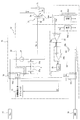
- FIG. 2 is a circuit of an intelligent power module including an overcurrent detection device according to a first embodiment of the present invention.
- the power conversion device to which the present invention can be applied is, as shown in FIG. 1, configured of an inverter circuit that converts, for example, DC power into three-phase AC power.
- This inverter circuit has a positive electrode side line 2 p connected to the positive electrode side of the main DC power supply 1 and a negative electrode side line 2 n connected to the negative electrode side of the main DC power supply 1.
- FWD Freewheel diodes
- connection point of the IGBTs 3A and 3B of the series circuit 4 a connection point of the IGBTs 3C and 3D of the series circuit 5, and a connection point of the IGBTs 3E and 3F of the series circuit 6 are connected to an inductance load 8 such as an electric motor.
- this inverter circuit will be described with reference to the signal waveform diagram of FIG. It is assumed that the IGBT 3A and the IGBT 3D are turned on at a certain timing, and the load 9 is supplied with the current I1 from the main DC power supply 1. Next, when the IGBTs 3A and 3D are turned off, the current I1 flowing to the load 9 flows as a return current to the main DC power supply 1 through the FWDs 7B and 7C. Thus, three phases of power are supplied to the load 9 by turning on and off the IGBTs 3A to 3F sequentially.
- IGBT drive circuit 10 has P channel MOSFET 10a and N channel MOSFET 10b connected in series between control power supply 15 and ground 16, and the connection point between P channel MOSFET 10a and N channel MOSFET 10b is gate 3g of IGBT 3i. It is connected to the.
- the driver IC 11 with a protection function controls the P-channel MOSFET 10 a and the N-channel MOSFET 10 b constituting the IGBT drive circuit 10 such that the other is in the off state when one is in the on state.
- the driver IC 11 with protection function turns on the P-channel MOSFET 10a and turns off the N-channel MOSFET 10b.
- the gate current Ig is supplied from the control power supply 15 to the gate 3g of the IGBT 3i to charge the gate capacitance (here, it represents the capacitance between the gate and the emitter).
- the P channel MOS VET 10a is turned off, the N channel MOSFET 10b is turned on, and the gate 3g of the IGBT 3i is connected to the ground 16 to discharge the gate capacitance.
- the overcurrent detection device 12 includes a sense emitter current detection unit 21, a correction current detection unit 22, a voltage correction unit 23, a comparison unit 24, and a low pass filter circuit 25.
- Sense emitter current detection unit 21 is connected between sense emitter 3se, which outputs a sense emitter current Ise of several thousandths to a few tens of thousands of collector current Ic flowing through collector 3c formed in IGBT 3i, and ground. It is composed of the current detection resistor Rs1. Then, the sense emitter voltage Vse obtained by converting the sense emitter current Ise into a voltage is output from the high potential side of the current detection resistor Rs1.
- the correction current detection unit 22 is connected between the current mirror circuit 31 whose input unit is connected to the drain side of the P-channel MOSFET 10 a of the IGBT drive circuit 10, and the output unit of the current mirror circuit 31 and the ground 16. And at least a current detection resistor Rs2.
- the current mirror circuit 31 includes a P channel MOSFET 31a connected between the drain of the P channel MOSFET 10a of the IGBT drive circuit 10 and the gate 3g of the IGBT 3i, and a P channel MOSFET 31b whose gate is connected to the gate of the P channel MOSFET 31a. It is configured.
- connection point between the gates of the P-channel MOSFETs 31a and 31b is connected to the connection point between the drains of the P-channel MOSFET 31a and the P-channel MOSFET 10a. Further, the drain of the P-channel MOSFET 31b is connected to the control power supply 15 via the constant current circuit 32, and the source is connected to the high potential side of the current detection resistor Rs2.
- the correction mirror current Iga is obtained such that the current mirror ratio of the current mirror circuit 31 is a current value corresponding to the gate current component superimposed on the sense emitter current Ise output from the sense emitter 3se of the IGBT 3i. It is set to. Then, the correction gate current Iga corresponding to the gate current included in the sense emitter current Ise output from the source of the P-channel MOSFET 31b of the current mirror circuit 31 is supplied to the current detection resistor Rs2. Therefore, the correction voltage Va obtained by converting the correction gate current Iga into a voltage is output from the high potential side of the current detection resistor Rs2.
- the voltage correction unit 23 is configured by an operational amplifier 23a that performs differential amplification.
- the sense emitter voltage Vse obtained from the high potential side of the current detection resistor Rs1 of the sense emitter current detection unit 21 is applied to the non-inversion input terminal of the operational amplifier 23a, and the current of the correction current detection unit 22 is applied to the inversion input terminal.
- a correction voltage Va obtained from the high potential side of the detection resistor Rs2 is applied. Therefore, a sense emitter correction voltage Vsea obtained by subtracting the correction voltage Va from the sense emitter voltage Vse is output from the operational amplifier 23a.
- the comparison unit 24 is configured of an overcurrent detection comparator 24a.
- the sense emitter correction voltage Vsea output from the above-described voltage correction unit 23 is applied to the non-inverted input terminal of the overcurrent detection comparator 24a, and the reference power supply 24b that outputs the overcurrent threshold voltage Vth is applied to the inverted input terminal. It is connected.
- An overcurrent detection signal Soc which is inverted from L level to H level is output from the overcurrent detection comparator 24a when the sense emitter correction voltage Vsea becomes higher than the overcurrent threshold voltage Vth.
- the overcurrent detection signal Soc output from the comparison unit 24 is supplied to the low pass filter circuit 25, and the filter output Sf low-pass filtered by the low pass filter circuit 25 is supplied to the driver IC 11 with protection function.
- the driver IC 11 with protection function compares the filter output Sf input from the low pass filter circuit 25 with the reference voltage Vref, and determines that the overcurrent state is obtained when Sf> Vref, thereby determining the P channel MOSFET 10a of the IGBT drive circuit 10.
- the gate signal to the gate of the MOSFET is turned off, and the gate signal to the gate of the N-channel MOSFET 10b is turned on to stop the driving of the IGBT 3i.
- the collector current Ic rises as shown in FIG. 3A, and the collector-emitter voltage Vce starts to fall as shown in FIG.
- the sense emitter current Ise which is about a few thousandths to a few thousandths of a fraction of the collector current Ic, rises and both ends of the current detection resistor Rs1 through which the sense emitter current Is flows
- the voltage, that is, the sense emitter voltage Vse also rises as shown in FIG. At this time, as shown in FIG.
- the gate capacitance of the sense emitter current Ise is charged to a collector current component of about several thousandths to a few tens of thousandths of the original collector current Ic.
- the gate current component proportional to the gate current Ig which flows until then is superimposed.
- the gate voltage Vg reaches the gate threshold voltage Vgth
- the collector-emitter voltage Vce decreases
- the mirror capacitance (gate-collector capacitance) of the IGBT 100 increases
- the gate voltage Vg shifts to a substantially constant region Do.
- the sense emitter current Ise also rises as shown in FIG. 3 (d)
- the sense emitter voltage Vse also rises as shown by the dotted line in FIG. 3 (f).
- the correction gate current Iga rises as shown in FIG. 3C, and begins to decrease gradually when the gate voltage Vg reaches the gate threshold voltage Vgth. Accordingly, the corrected sense emitter current Isea obtained by subtracting the correction gate current Iga from the sense emitter current Ise is as shown in FIG. 3E, and the amplitude is suppressed compared to the sense emitter current Ise.
- the sense emitter current detection unit 21 detects the sense emitter current Ise as the sense emitter voltage Vse, and applies the sense emitter voltage Vse to the non-inverting input terminal of the operational amplifier 23 a of the voltage correction unit 23.
- the correction current detection unit 22 detects the correction gate current Iga as the correction gate voltage Vga, and applies the correction gate voltage Vga to the inverting input terminal of the operational amplifier 23a of the voltage correction unit 23.
- the operational amplifier 23a subtracts the correction gate voltage Vga from the sense emitter voltage Vse to output the sense emitter correction voltage Vsea.
- the sense emitter correction voltage Vsea removes the gate current component by removing the correction gate voltage Vga from the sense emitter voltage Vse, and the amplitude due to only the collect current component is suppressed.
- the voltage is
- the detection prevention time T2 is shortened to about 1 ⁇ sec, and can be shortened to one fourth to one fifth of the erroneous detection prevention time T1 in the conventional example.
- the time constant of the low pass filter circuit 25 connected to the output side of the overcurrent detection comparator 24a is as short as one-quarter to one-fifth that of the conventional low-pass filter circuit 103 described above. can do. Therefore, the erroneous detection preventing time T2 and the actual overcurrent state are detected when the overcurrent state is determined in the normal switching state except the turn-on, while preventing the erroneous detection at the turn-on of the IGBT 3i.
- the determination time including the detection time Td required when performing this can be made sufficiently short, and accurate overcurrent detection becomes possible.
- the configuration of the overcurrent detection device 12 can be miniaturized.
- the overcurrent determination time can be shortened, even when a short circuit current flows in the IGBT, the short circuit current can be detected immediately, and a separate short circuit current detection circuit can be provided. Short circuit detection can be performed without providing, and the circuit configuration of the IGBT protection circuit can be simplified and miniaturized. Moreover, by applying the current mirror circuit 31 that detects the gate current Ig of the IGBT 3i as the correction current detection unit 22, the current mirror ratio can be adjusted. Therefore, the correction gate current Iga corresponding to the sense emitter current output from the sense emitter 3se of the IGBT 3i can be accurately detected.
- the sense emitter current detection unit 21 and the correction current detection unit 22 use the current detection resistors Rs1 and Rs2 to detect the current as a voltage value. Therefore, by adjusting at least one of the resistance values of the current detection resistors Rs1 and Rs2, it is possible to adjust the sense emitter voltage Vse and the voltage value of the correction gate voltage Vga to appropriate values. For this reason, more accurate overcurrent detection can be performed.
- the intelligent power module 13 can be further enhanced by configuring the intelligent power module 13 by integrating the IGBT 3i, the FWD 7i, the IGBT drive circuit 10, the driver IC 11 with protection function, and the overcurrent detection device 12 described above into one package. It can be miniaturized.
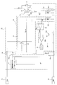
- the configuration of the correction current detection unit 22 is changed. That is, in the second embodiment, as shown in FIG. 4, in the correction current detection unit 22, the current mirror circuit 31 and the constant current circuit 32 are omitted, and instead, they are gate control signals of the driver IC with protection function.
- a P-channel MOSFET 33 is provided which is driven by the The drain of the P-channel MOSFET 33 is connected to the control power supply 15, and the source is connected to the high potential side of the current detection resistor Rs2.
- the P-channel MOSFET 33 is set to a cell size smaller than the cell size of the P-channel MOSFET 10 a of the IGBT drive circuit 10.
- the cell size ratio of P channel MOSFETs 10a and 33 in this case is set to be equal to the current mirror ratio of current mirror circuit 31 described above, and correction gate current Ig output from P channel MOSFET 33 is the sense emitter 3se of IGBT 3i.
- the correction gate current Iga similar to that of the P channel MOSFET 31b of the current mirror circuit 31 described above is output from the P channel MOSFET 33, and the correction gate current Iga is supplied to the current detection resistor Rs2. Therefore, the correction gate voltage Vga corresponding to the correction gate current Iga is obtained from the high potential side of the current detection resistor Rs2.
- the voltage correction unit 33 subtracts the correction gate voltage Vga from the sense emitter voltage Vse to calculate the correction sense emitter voltage Vsea, which is output to the comparison unit 34.
- the correction current detection unit 22 can be configured only by providing the P-channel MOSFET 33 having a size ratio different from that of the P-channel MOSFET 10a of the IGBT drive circuit 10 and the current detection resistor Rs2. The configuration of the correction current detection unit 22 can be miniaturized.
- the low-pass filter circuit 25 is provided on the output side of the comparing unit 24 for detecting an overcurrent, but the present invention is not limited to this.
- a filter circuit 25 may be provided to supply the filter output of the low pass filter circuit 25 to the overcurrent detection comparator 24a.
- the correction sense emitter voltage is calculated by subtracting the correction voltage corresponding to the current between the gate of the IGBT and the sense emitter from the sense emitter voltage corresponding to the sense emitter current of the IGBT. Therefore, it is possible to provide an overcurrent detection device capable of shortening the erroneous current detection prevention time of the overcurrent at the time of turn-on operation of the IGBT, and an intelligent power module using the same.
Landscapes
- Engineering & Computer Science (AREA)
- Power Engineering (AREA)
- Physics & Mathematics (AREA)
- General Physics & Mathematics (AREA)
- Electronic Switches (AREA)
- Power Conversion In General (AREA)
Abstract
誤検出防止時間を短縮することができる過電流検出装置及びこれを使用したインテリジェントパワーモジュールを提供する。IGBT(3i)のセンスエミッタ(3se)から出力されるセンスエミッタ電流をセンスエミッタ電圧として検出するセンスエミッタ電流検出部(21)と、該センスエミッタ電流検出部で検出したセンスエミッタ電圧と閾値電圧とを比較して過電流を検出する比較部(24)とを備えている。さらに、前記IGBTのゲート及びセンスエミッタ間の電流に対応する補正用電流を補正電圧として検出する補正用電流検出部(22)と、前記センスエミッタ電流検出部で検出したセンスエミッタ電圧から前記補正電流検出部で検出した補正用電圧を減じてセンスエミッタ補正電圧を算出し、当該センスエミッタ補正電圧を前記比較部に供給する電圧補正部(23)とを備えている。
Description
本発明は、絶縁ゲートバイポーラトランジスタ(以下、IGBTと称す)に過電流が流れたときに、IGBTを破壊から保護する過電流検出装置及びこれを使用したインテリジェントパワーモジュールに関する。
電力変換装置を構成する三相のインバータ回路は、6個のIGBTと、これらIGBTと逆並列に接続されたフリーホイールダイオード(FWD)とが2つずつ直列に接続された直列回路が直流電源に並列に接続された構成を有し、各直列回路のIGBT間の接続点に電動モータなどのインダクタンス負荷が接続されている。
このような電力変換装置に使用されるIGBTでは、過電流が流れたときにIGBTを破壊から保護するために過電流保護回路が設けられている。
このような電力変換装置に使用されるIGBTでは、過電流が流れたときにIGBTを破壊から保護するために過電流保護回路が設けられている。
この過電流保護回路としては、図5に示す構成が知られている。
IGBT100には、コレクタ100cと、エミッタ100eと、センスエミッタ100seとが設けられている。センスエミッタ100seは、コレクタ100cとエミッタ100eの間を流れる電流に対して数千分の1又は数万分の1程度のセンス電流を出力する。この過電流保護回路は、センスエミッタ100seと接地との間に電流検出用抵抗101を介挿し、この電流検出用抵抗101の高電位側のセンス電圧Vseを過電流検出用コンパレータ102の非反転入力端子に入力する。
IGBT100には、コレクタ100cと、エミッタ100eと、センスエミッタ100seとが設けられている。センスエミッタ100seは、コレクタ100cとエミッタ100eの間を流れる電流に対して数千分の1又は数万分の1程度のセンス電流を出力する。この過電流保護回路は、センスエミッタ100seと接地との間に電流検出用抵抗101を介挿し、この電流検出用抵抗101の高電位側のセンス電圧Vseを過電流検出用コンパレータ102の非反転入力端子に入力する。
この過電流検出用コンパレータ102の反転入力端子には、過電流を判断する閾値電圧Vthが入力され、この過電流検出用コンパレータ102からセンス電圧Vseが閾値電圧Vth以上となったときにオフ状態からオン状態に反転する過電流検出信号Socが出力される。
この過電流検出信号Socは、ローパスフィルタ回路103に供給されて所定の時定数を持って積分されることにより、IGBT100のターンオン時に生じるセンス電圧Vseが閾値電圧Vthを超える値となる過渡的な増加状態で過電流の誤検出を防止するようにしている。
この過電流検出信号Socは、ローパスフィルタ回路103に供給されて所定の時定数を持って積分されることにより、IGBT100のターンオン時に生じるセンス電圧Vseが閾値電圧Vthを超える値となる過渡的な増加状態で過電流の誤検出を防止するようにしている。
なお、IGBT100は、ゲート駆動回路105から供給されるゲート電流によって駆動制御される。このゲート駆動回路105は、制御電源106及びグランド107間に直列に接続されたPチャネルMOSFET108及びNチャネルMOSFET109を有し、これらPチャネルMOSFET108及びNチャネルMOSFET109の接続点がIGBT100のゲート100gに接続されている。そして、PチャネルMOSFET108及びNチャネルMOSFET109が保護機能付きドライバIC110によって、一方がオン状態であるときに他方がオフ状態となるように制御される。
上記過電流保護回路の動作を図6の信号波形図を用いて説明する。
IGBT駆動回路のPチャネルMOSFET108がオンすると、制御電源106の電圧Vcc(例えば15V程度)と等しい制御電圧VgccがIGBT100のゲート100gに印加される。
IGBT100は、絶縁ゲート型の半導体デバイスであり、いわゆる電圧駆動型のデバイスであるが、IGBT100のゲート100gにはゲート電流Igが流れ、ゲート容量(ここではゲート・エミッタ間容量のこと)を充電する。ゲート容量が充電されると図6(b)に示すようにゲート電圧Vgが立ち上がる。ゲート電圧Vgが立ち上がりゲート閾値電圧に達すると、図6(a)に示すようにコレクタ電流Icが立ち上がり、コレクタ・エミッタ間電圧Vceは図6(a)に示すように立下がり始める。
IGBT駆動回路のPチャネルMOSFET108がオンすると、制御電源106の電圧Vcc(例えば15V程度)と等しい制御電圧VgccがIGBT100のゲート100gに印加される。
IGBT100は、絶縁ゲート型の半導体デバイスであり、いわゆる電圧駆動型のデバイスであるが、IGBT100のゲート100gにはゲート電流Igが流れ、ゲート容量(ここではゲート・エミッタ間容量のこと)を充電する。ゲート容量が充電されると図6(b)に示すようにゲート電圧Vgが立ち上がる。ゲート電圧Vgが立ち上がりゲート閾値電圧に達すると、図6(a)に示すようにコレクタ電流Icが立ち上がり、コレクタ・エミッタ間電圧Vceは図6(a)に示すように立下がり始める。
また、コレクタ電流Icの数千分の1~数万分の1程度であるセンス電流Iseが図6(c)に示すように立ち上がり、センス電流Iseが流れるセンス抵抗Rsの両端の電圧、つまりセンス電圧Vseも図6(d)に示すように上昇する。ゲート電圧Vgがゲート閾値電圧に達すると、コレクタ・エミッタ間電圧Vceが低下し、IGBT100のミラー容量(ゲート・コレクタ容量)が増大して、ゲート電圧Vgはほぼ一定となる領域に移行する。
この間に、センス電流Iseも図6(c)に示すように上昇し、これに伴ってセンス電圧Vseも図6(d)に示すように上昇し、過電流と判断する過電流閾値電圧Vth(これは基準電圧Eで決まる)に達すると、過電流検出用コンパレータ102の出力はHレベルの過電流検出信号Socを出力する。
この過電流検出信号Socはローパスフィルタ回路103に供給されるので、ローパスフィルタ回路103の出力は、緩やかに上昇する。このとき、ローパスフィルタ回路103の時定数をセンス電圧Vsが過電流閾値電圧Vthを超えてから過電流閾値電圧Vth以下となるまでの誤検出防止時間T1よりも大きく設定されている。
この過電流検出信号Socはローパスフィルタ回路103に供給されるので、ローパスフィルタ回路103の出力は、緩やかに上昇する。このとき、ローパスフィルタ回路103の時定数をセンス電圧Vsが過電流閾値電圧Vthを超えてから過電流閾値電圧Vth以下となるまでの誤検出防止時間T1よりも大きく設定されている。
このため、センス電圧Vseが過電流閾値電圧Vthを超えている誤検出防止時間T1の間にローパスフィルタ回路103のフィルタ出力が過電流検出用コンパレータ102のHレベルに達することはない。
このため、ローパスフィルタ回路103のフィルタ出力が保護機能付きドライバIC110に供給されたときに、フィルタ出力が過電流検出用コンパレータ102のHレベルに達することがない。したがって、保護機能付きドライバIC110でゲート電流Igが遮断されることはない。
このため、ローパスフィルタ回路103のフィルタ出力が保護機能付きドライバIC110に供給されたときに、フィルタ出力が過電流検出用コンパレータ102のHレベルに達することがない。したがって、保護機能付きドライバIC110でゲート電流Igが遮断されることはない。
しかしながら、過電流検出用コンパレータ102から出力される過電流検出信号SocのHレベルが誤検出防止時間T1を超えて継続される場合には、ローパスフィルタ回路103のフィルタ出力がHレベルに達する。このため、保護機能付きドライバIC110でIGBT100のゲート100gに対するゲート電流Igの出力が停止されて、IGBT100の過電流保護機能が動作する。
また、上記図5の構成では、ローパスフィルタ回路103を使用してIGBT100のターンオン時の過電流誤検出を防止するようにした場合について説明したが、特許文献1に記載されているように構成することもできる。
すなわち、特許文献1では、ローパスフィルタ回路を省略してIGBTを動作させる入力信号の立ち上がりのエッジを検出してタイマーを動作させるようにしている。したがって、前述した誤検出防止時間T1の間通常の基準電圧より高い基準電圧を過電流検出用コンパレータに供給して、センス電圧Vseが過電流閾値電圧Vthを超えている期間過電流検出用コンパレータから出力される過電流検出信号がLレベルを維持するようにしている。
すなわち、特許文献1では、ローパスフィルタ回路を省略してIGBTを動作させる入力信号の立ち上がりのエッジを検出してタイマーを動作させるようにしている。したがって、前述した誤検出防止時間T1の間通常の基準電圧より高い基準電圧を過電流検出用コンパレータに供給して、センス電圧Vseが過電流閾値電圧Vthを超えている期間過電流検出用コンパレータから出力される過電流検出信号がLレベルを維持するようにしている。
ところで、上記従来例によると、ローパスフィルタ回路を使用して過電流検出用コンパレータ102から出力されるHレベルの過電流検出信号SocのHレベルの立ち上がりをなまらせるか、タイマーを使用して誤検出防止時間T1の間過電流検出用コンパレータに通常の基準電圧より高い基準電圧を加えるようにしている。これにより、IGBTのターンオン時に生じるセンス電圧Vseが過電流閾値電圧Vthを超えている期間での誤検出を防止するようにしている。
しかしながら、上記従来例では、ローパスフィルタ回路を使用する場合には、IGBTの誤検出防止時間T1が4~5μsecと比較的長く、この誤検出防止時間T1が経過してから過電流判断を行うことになる。このため、過電流状態となったときに、過電流状態と判断するまでの判断時間が長くなるという未解決の課題がある。しかも、誤検出防止時間T1はIGBTによって異なるので、ローパスフィルタ回路の時定数を長めに設定せざるを得ず、この点でも過電流状態と判断する判断時間が長くなるという未解決の課題がある。このため、短時間の判断を必要とする短絡電流の検出を同時に行うことはできない。
これに対して、特許文献1に記載された発明では、タイマーを使用して過電流検出用コンパレータの基準電圧を変更する場合には、ローパスフィルタを使用しないので、時定数の設定の必要はない。しかしながら、特許文献1に記載された発明では、タイマーに誤検出防止時間T1に相当する比較的長いタイムアップ時間を設定する必要がある。この誤検出防止時間T1はIGBTによって異なるので、タイムアップ時間を長めに設定する必要があるという未解決の課題がある。さらに、特許文献1に記載された発明では、タイマー、スイッチ回路、2種類の基準電圧源等を設ける必要があり、回路構成が大型化するという未解決の課題もある。
そこで、本発明は、上記従来例の未解決の課題に着目してなされたものであり、誤検出防止時間を短縮することができる過電流検出装置及びこれを使用したインテリジェントパワーモジュールを提供することを目的としている。
そこで、本発明は、上記従来例の未解決の課題に着目してなされたものであり、誤検出防止時間を短縮することができる過電流検出装置及びこれを使用したインテリジェントパワーモジュールを提供することを目的としている。
上記目的を達成するために、本発明の第1の態様は、絶縁ゲートバイポーラトランジスタのセンスエミッタから出力されるセンスエミッタ電流をセンスエミッタ電圧として検出するセンスエミッタ電流検出部と、該センスエミッタ電流検出部で検出したセンスエミッタ電圧と閾値電圧とを比較して過電流を検出する比較部とを備えた過電流検出装置である。そして、過電流検出装置は、前記絶縁ゲートバイポーラトランジスタのゲート及びセンスエミッタ間の電流に対応する補正用電流を補正電圧として検出する補正用電流検出部と、前記センスエミッタ電流検出部で検出したセンスエミッタ電圧から前記補正電流検出部で検出した補正用電圧を減じてセンスエミッタ補正電圧を算出し、当該センスエミッタ補正電圧を前記比較部に供給する電圧補正部とを備えている。
また、本発明に係る過電流検出装置の第2の態様は、前記センス電流検出部及び前記補正電流検出部が、電流検出用抵抗を有し、電流を電圧値として検出するように構成されている。
また、本発明に係る過電流検出装置の第3の態様は、前記補正用電流検出部が、前記ゲートに供給する電流路に介挿したカレントミラー回路と、該カレントミラー回路の電流出力部と接地との間に介挿した前記電流検出用抵抗とで構成されている。
また、本発明に係る過電流検出装置の第3の態様は、前記補正用電流検出部が、前記ゲートに供給する電流路に介挿したカレントミラー回路と、該カレントミラー回路の電流出力部と接地との間に介挿した前記電流検出用抵抗とで構成されている。
また、本発明に係る過電流検出装置の第4の態様は、前記補正用電流検出部が、前記絶縁ゲートバイポーラトランジスタのゲート電流を制御する第1の半導体電流制御素子と並列に配置した前記第1の半導体電流制御素子のセルサイズに比較して小さいセルサイズの第2の半導体電流制御素子と、該第2の半導体制御素子の出力側と接地との間に介挿した前記電流検出用抵抗とで構成されている。
また、本発明に係るインテリジェントパワーモジュールの第1の態様は、絶縁ゲートバイポーラトランジスタ及び当該絶縁ゲートバイポーラトランジスタと逆並列に接続されたフリーホイールダイオードと、上記第1~第4の態様の何れか1つの態様を備えた過電流検出装置と、前記絶縁ゲートバイポーラトランジスタの駆動と少なくとも前記過電流検出装置の過電流検出値に基づく前記絶縁ゲートバイポーラトランジスタの保護とを行う駆動用ICとを1つのパッケージに集約している。
本発明によれば、センスエミッタ電流検出部で検出したIGBTのセンスエミッタ電圧から補正電流検出部で検出したIGBTのゲート及びセンスエミッタ間の電流に対応する補正用電圧を減算して算出したセンスエミッタ補正電圧を過電流閾値電圧と比較するようにしている。このため、IGBTのコレクタ電流に相当する正味のセンスエミッタ電圧で過電流判断を行うので、IGBTのターンオン時の誤検出防止時間を短縮することができる。このため、過電流検出に加えて短絡電流検出にも適用することができる。
さらに、上記過電流検出装置と、IGBT、FWD、IGBTの駆動用ICとを1つのパッケージに集約してインテリジェンパワートモジュールを構成するので、全体の構成を小型化することができる。
さらに、上記過電流検出装置と、IGBT、FWD、IGBTの駆動用ICとを1つのパッケージに集約してインテリジェンパワートモジュールを構成するので、全体の構成を小型化することができる。
以下、本発明の実施の形態について図面を伴って説明する。
図1は、本発明を適用し得る電力変換装置を示す回路図、図2には、本発明の第1の実施形態における過電流検出装置を含むインテリジェントパワーモジュールの回路である。
本発明を適用し得る電力変換装置は、図1に示すように、例えば直流電力を三相交流電力に変換するインバータ回路で構成されている。このインバータ回路は、主直流電源1の正極側に接続された正極側ライン2pと主直流電源1の負極側に接続された負極側ライン2nとを有する。
図1は、本発明を適用し得る電力変換装置を示す回路図、図2には、本発明の第1の実施形態における過電流検出装置を含むインテリジェントパワーモジュールの回路である。
本発明を適用し得る電力変換装置は、図1に示すように、例えば直流電力を三相交流電力に変換するインバータ回路で構成されている。このインバータ回路は、主直流電源1の正極側に接続された正極側ライン2pと主直流電源1の負極側に接続された負極側ライン2nとを有する。
これら正極側ライン2p及び負極側ライン2n間に、絶縁ゲートバイポーラトランジスタ(以下、IGBTと称す)3A及び3Bを直列に接続した直列回路4と、IGBT3C及び3Dを直列に接続した直列回路5と、IGBT3E及び3Fを直列に接続した直列回路6とが並列に接続されている。各IGBT3A~3Fには、フリーホイールダイオード(以下、FWDと称す)7A~7Fが逆並列に接続されている。
そして、直列回路4のIGBT3A及び3Bの接続点、直列回路5のIGBT3C及び3Dの接続点並びに直列回路6のIGBT3E,3Fの接続点が電動モータ等のインダクタンス負荷8に接続されている。
そして、直列回路4のIGBT3A及び3Bの接続点、直列回路5のIGBT3C及び3Dの接続点並びに直列回路6のIGBT3E,3Fの接続点が電動モータ等のインダクタンス負荷8に接続されている。
このインバータ回路の動作を図3の信号波形図を伴って説明する。
あるタイミングでIGBT3AとIGBT3Dがオンして負荷9に主直流電源1から電流I1が供給されているものとする。つぎに、IGBT3AとIGBT3Dがオフすると負荷9に流れている電流I1はFWD7B,7Cを通して主直流電源1に還流電流となって流れ込む。このように、IGBT3A~IGBT3Fが順次オン・オフすることで、負荷9に三相の電力を供給する。
あるタイミングでIGBT3AとIGBT3Dがオンして負荷9に主直流電源1から電流I1が供給されているものとする。つぎに、IGBT3AとIGBT3Dがオフすると負荷9に流れている電流I1はFWD7B,7Cを通して主直流電源1に還流電流となって流れ込む。このように、IGBT3A~IGBT3Fが順次オン・オフすることで、負荷9に三相の電力を供給する。
ところで、IGBT3Aがオンからオフへ遷移し、電流I2がFWD7Cを流れている状態で、IGBT3Dがオンすると、一瞬、FWD7CとIGBT3Dの直列回路がアーム短絡状態になる。このアーム短絡はFWD7Cが逆回復した時に解消されるものの、IGBT3Dがターンオンするとき、このFWD7Cの逆回復電流がIGBT3Dのコレクタ電流に重畳して流れる。そのため、図3(a)に示すように、IGBT3Dのコレクタ電流Icはターンオン動作時には逆回復電流Irが重畳されるので跳ね上がり、その後定常状態に移行する。
そして、インバータ回路を構成する各IGBT3i及びFWD7i(i=A~F)のそれぞれは、図2に示すように、IGBT駆動回路10、保護機能付きドライバIC11、過電流検出装置12を含んで1つのパッケージ化されてインテリジェントパワーモジュール13として構成されている。
ここで、IGBT駆動回路10は、制御電源15及びグランド16間に直列に接続されたPチャネルMOSFET10aと、NチャネルMOSFET10bとを有し、PチャネルMOSFET10a及びNチャネルMOSFET10bの接続点がIGBT3iのゲート3gに接続されている。
ここで、IGBT駆動回路10は、制御電源15及びグランド16間に直列に接続されたPチャネルMOSFET10aと、NチャネルMOSFET10bとを有し、PチャネルMOSFET10a及びNチャネルMOSFET10bの接続点がIGBT3iのゲート3gに接続されている。
保護機能付きドライバIC11は、IGBT駆動回路10を構成するPチャネルMOSFET10a及びNチャネルMOSFET10bを一方がオン状態であるときに他方がオフ状態となるように制御する。この保護機能付きドライバIC11は、IGBT3iをターンオンさせる場合には、PチャネルMOSFET10aをオン状態とし、NチャネルMOSFET10bをオフ状態とする。これにより、制御電源15からゲート電流IgをIGBT3iのゲート3gに供給してゲート容量(ここではゲート・エミッタ間容量を表す)を充電する。逆に、IGBT3iをターンオフさせる場合には、PチャネルMOSVET10aをオフ状態とし、NチャネルMOSFET10bをオン状態としてIGBT3iのゲート3gをグランド16に接続してゲート容量を放電する。
過電流検出装置12は、センスエミッタ電流検出部21と、補正用電流検出部22と、電圧補正部23、比較部24と、ローパスフィルタ回路25とを備えている。
センスエミッタ電流検出部21は、IGBT3iに形成されたコレクタ3cを流れるコレクタ電流Icの数千分1~数万分の1程度のセンスエミッタ電流Iseを出力するセンスエミッタ3seとグランドとの間に接続された電流検出用抵抗Rs1で構成されている。そして、電流検出用抵抗Rs1の高電位側からセンスエミッタ電流Iseが電圧に変換されたセンスエミッタ電圧Vseが出力される。
センスエミッタ電流検出部21は、IGBT3iに形成されたコレクタ3cを流れるコレクタ電流Icの数千分1~数万分の1程度のセンスエミッタ電流Iseを出力するセンスエミッタ3seとグランドとの間に接続された電流検出用抵抗Rs1で構成されている。そして、電流検出用抵抗Rs1の高電位側からセンスエミッタ電流Iseが電圧に変換されたセンスエミッタ電圧Vseが出力される。
補正用電流検出部22は、IGBT駆動回路10のPチャネルMOSFET10aのドレイン側に入力部が接続されたカレントミラー回路31と、このカレントミラー回路31の出力部とグランド16との間に接続された電流検出用抵抗Rs2とを少なくとも有する。
カレントミラー回路31は、IGBT駆動回路10のPチャネルMOSFET10aのドレインとIGBT3iのゲート3gとの間に接続されたPチャネルMOSFET31aと、このPチャネルMOSFET31aのゲートにゲートが接続されたPチャネルMOSFET31bとで構成されている。
カレントミラー回路31は、IGBT駆動回路10のPチャネルMOSFET10aのドレインとIGBT3iのゲート3gとの間に接続されたPチャネルMOSFET31aと、このPチャネルMOSFET31aのゲートにゲートが接続されたPチャネルMOSFET31bとで構成されている。
そして、PチャネルMOSFET31a及び31bのゲート間の接続点がPチャネルMOSFET31a及びPチャネルMOSFET10aのドレイン間の接続点に接続されている。また、PチャネルMOSFET31bのドレインが定電流回路32を介して制御電源15に接続され、ソースが電流検出用抵抗Rs2の高電位側に接続されている。
ここで、カレントミラー回路31のカレントミラー比は、IGBT3iのセンスエミッタ3seから出力されるセンスエミッタ電流Iseに重畳されているゲート電流成分に対応する電流値となる補正用ゲート電流Igaが得られるように設定されている。そして、カレントミラー回路31のPチャネルMOSFET31bのソースから出力されるセンスエミッタ電流Iseに含まれるゲート電流分に相当する補正用ゲート電流Igaが電流検出用抵抗Rs2に供給される。
したがって、電流検出用抵抗Rs2の高電位側から補正用ゲート電流Igaが電圧に変換された補正用電圧Vaが出力される。
したがって、電流検出用抵抗Rs2の高電位側から補正用ゲート電流Igaが電圧に変換された補正用電圧Vaが出力される。
電圧補正部23は、差動増幅を行うオペアンプ23aで構成されている。このオペアンプ23aの非反転入力端子にはセンスエミッタ電流検出部21の電流検出用抵抗Rs1の高電位側から得られるセンスエミッタ電圧Vseが印加され、反転入力端子には補正用電流検出部22の電流検出用抵抗Rs2の高電位側から得られる補正用電圧Vaが印加されている。したがって、オペアンプ23aからセンスエミッタ電圧Vseから補正用電圧Vaを減算したセンスエミッタ補正電圧Vseaが出力される。
比較部24は、過電流検出用コンパレータ24aで構成されている。この過電流検出用コンパレータ24aの非反転入力端子には上述した電圧補正部23から出力されるセンスエミッタ補正電圧Vseaが印加され、反転入力端子には過電流閾値電圧Vthを出力する基準電源24bが接続されている。過電流検出用コンパレータ24aからセンスエミッタ補正電圧Vseaが過電流閾値電圧Vth以上となったときにLレベルからHレベルに反転する過電流検出信号Socが出力される。
そして、比較部24から出力される過電流検出信号Socがローパスフィルタ回路25に供給されて、このローパスフィルタ回路25でローパスフィルタ処理されたフィルタ出力Sfが保護機能付きドライバIC11に供給される。
この保護機能付きドライバIC11では、ローパスフィルタ回路25から入力されるフィルタ出力Sfを基準電圧Vrefと比較し、Sf>Vrefであるときに過電流状態である判断してIGBT駆動回路10のPチャネルMOSFET10aのゲートに対するゲート信号をオフ状態とし、NチャネルMOSFET10bのゲートに対するゲート信号をオン状態としてIGBT3iの駆動を停止する。
この保護機能付きドライバIC11では、ローパスフィルタ回路25から入力されるフィルタ出力Sfを基準電圧Vrefと比較し、Sf>Vrefであるときに過電流状態である判断してIGBT駆動回路10のPチャネルMOSFET10aのゲートに対するゲート信号をオフ状態とし、NチャネルMOSFET10bのゲートに対するゲート信号をオン状態としてIGBT3iの駆動を停止する。
次に、上記第1の実施形態の動作を図3の信号波形図を伴って説明する。
IGBT駆動回路10のPチャネルMOSFET10aがオンすると、制御電源15の電圧Vcc(例えば15V程度)と等しい制御電圧VgccがIGBT3iのゲート3gに印加される。
IGBT3iのゲート3gにはゲート電流Igが流れ、ゲート容量(ここではゲート・エミッタ間容量を表す)を充電する。ゲート容量が充電されると図3(b)に示すようにゲート電圧Vgが立ち上がる。このとき、カレントミラー回路31のPチャネルMOSFET31bからゲート電流Igに比例し、センスエミッタ電流Iseに対応する補正用ゲート電流Igaが図3(c)に示すように出力開始される。
IGBT駆動回路10のPチャネルMOSFET10aがオンすると、制御電源15の電圧Vcc(例えば15V程度)と等しい制御電圧VgccがIGBT3iのゲート3gに印加される。
IGBT3iのゲート3gにはゲート電流Igが流れ、ゲート容量(ここではゲート・エミッタ間容量を表す)を充電する。ゲート容量が充電されると図3(b)に示すようにゲート電圧Vgが立ち上がる。このとき、カレントミラー回路31のPチャネルMOSFET31bからゲート電流Igに比例し、センスエミッタ電流Iseに対応する補正用ゲート電流Igaが図3(c)に示すように出力開始される。
そして、ゲート電圧Vgが立ち上がりゲート閾値電圧Vgthに達すると、図3(a)に示すようにコレクタ電流Icが立ち上がり、コレクタ・エミッタ間電圧Vceは図3(a)に示すように立下がり始める。
また、コレクタ電流Icの数千分の1~数万分の1程度であるセンスエミッタ電流Iseが図3(c)に示すように立ち上がり、センスエミッタ電流Iseが流れる電流検出用抵抗Rs1の両端の電圧、つまりセンスエミッタ電圧Vseも図3(d)に示すように上昇する。このとき、センスエミッタ電流Iseには、図3(d)に示すように、本来のコレクタ電流Icの数千分の1~数万分の1程度のコレクタ電流成分に、ゲート容量が充電されるまでの間に流れるゲート電流Igに比例するゲート電流成分が重畳されている。
また、コレクタ電流Icの数千分の1~数万分の1程度であるセンスエミッタ電流Iseが図3(c)に示すように立ち上がり、センスエミッタ電流Iseが流れる電流検出用抵抗Rs1の両端の電圧、つまりセンスエミッタ電圧Vseも図3(d)に示すように上昇する。このとき、センスエミッタ電流Iseには、図3(d)に示すように、本来のコレクタ電流Icの数千分の1~数万分の1程度のコレクタ電流成分に、ゲート容量が充電されるまでの間に流れるゲート電流Igに比例するゲート電流成分が重畳されている。
その後、ゲート電圧Vgがゲート閾値電圧Vgthに達すると、コレクタ・エミッタ間電圧Vceが低下し、IGBT100のミラー容量(ゲート・コレクタ容量)が増大して、ゲート電圧Vgはほぼ一定となる領域に移行する。
この間に、センスエミッタ電流Iseも図3(d)に示すように上昇し、これに伴ってセンスエミッタ電圧Vseも図3(f)で点線図示のように上昇する。
この間に、センスエミッタ電流Iseも図3(d)に示すように上昇し、これに伴ってセンスエミッタ電圧Vseも図3(f)で点線図示のように上昇する。
また、補正用ゲート電流Igaは、図3(c)に示すように上昇し、ゲート電圧Vgがゲート閾値電圧Vgthに達すると緩やかに減少をはじめる。
したがって、センスエミッタ電流Iseから補正用ゲート電流Igaを減算した補正センスエミッタ電流Iseaは、図3(e)に示すようになり、センスエミッタ電流Iseに比較して振幅が抑制される。
したがって、センスエミッタ電流Iseから補正用ゲート電流Igaを減算した補正センスエミッタ電流Iseaは、図3(e)に示すようになり、センスエミッタ電流Iseに比較して振幅が抑制される。
本実施形態では、センスエミッタ電流検出部21で、センスエミッタ電流Iseをセンスエミッタ電圧Vseとして検出し、このセンスエミッタ電圧Vseを電圧補正部23のオペアンプ23aの非反転入力端子に印加する。一方、補正用電流検出部22で、補正用ゲート電流Igaを補正用ゲート電圧Vgaとして検出し、この補正用ゲート電圧Vgaを電圧補正部23のオペアンプ23aの反転入力端子に印加する。
したがって、オペアンプ23aでは、センスエミッタ電圧Vseから補正用ゲート電圧Vgaを減算してセンスエミッタ補正電圧Vseaを出力する。このセンスエミッタ補正電圧Vseaは、図3(f)で実線図示のように、センスエミッタ電圧Vseから補正用ゲート電圧Vgaを除くことにより、ゲート電流成分を除去してコレクト電流成分のみによる振幅が抑制された電圧となる。
このセンスエミッタ補正電圧Vseaは、図3(f)で点線図示の前述した従来例におけるセンスエミッタ電圧Vse′に対して振幅が大幅に小さくなるため、IGBT3iのターンオン時に過電流閾値電圧Vthを超える誤検出防止時間T2が1μsec程度と短くなり、従来例における誤検出防止時間T1の4分の1~5分の1に短縮することができる。
したがって、過電流検出用コンパレータ24aの出力側に接続されるローパスフィルタ回路25の時定数を前述した従来例のローパスフィルタ回路103の時定数に比較して4分の1~5分の1に短くすることができる。
このため、IGBT3iのターンオン時を過電流時の誤検出を防止しながら、ターンオン時を除く通常スイッチング状態で、過電流状態を判断する場合に、誤検出防止時間T2及び実際に過電流状態を検出する際に必要とする検出時間Tdを含めた判断時間を十分に短くすることができ、精度の高い過電流検出が可能となる。しかも、前述した特許文献1に記載されているタイマーを必要としないので、過電流検出装置12の構成を小型化することができる。
このため、IGBT3iのターンオン時を過電流時の誤検出を防止しながら、ターンオン時を除く通常スイッチング状態で、過電流状態を判断する場合に、誤検出防止時間T2及び実際に過電流状態を検出する際に必要とする検出時間Tdを含めた判断時間を十分に短くすることができ、精度の高い過電流検出が可能となる。しかも、前述した特許文献1に記載されているタイマーを必要としないので、過電流検出装置12の構成を小型化することができる。
このように本実施形態によると、過電流判断時間を短縮することができるので、IGBTに短絡電流が流れた場合にも、短絡電流を即座に検出することができ、別途短絡電流検出用回路を設けることなく、短絡検出が可能となり、IGBT保護回路の回路構成を簡素化することができるとともに、小型化することができる。
しかも、補正用電流検出部22としてIGBT3iのゲート電流Igを検出するカレントミラー回路31を適用することにより、カレントミラー比を調整することができる。したがって、IGBT3iのセンスエミッタ3seから出力されるセンスエミッタ電流に対応する補正用ゲート電流Igaを正確に検出することができる。
しかも、補正用電流検出部22としてIGBT3iのゲート電流Igを検出するカレントミラー回路31を適用することにより、カレントミラー比を調整することができる。したがって、IGBT3iのセンスエミッタ3seから出力されるセンスエミッタ電流に対応する補正用ゲート電流Igaを正確に検出することができる。
さらに、センスエミッタ電流検出部21及び補正用電流検出部22で電流検出用抵抗Rs1及びRs2を使用して電流を電圧値として検出している。このため、各電流検出用抵抗Rs1及びRs2の抵抗値の少なくとも一方を調整することにより、センスエミッタ電圧Vseと補正用ゲート電圧Vgaの電圧値とを適正値に調整することができる。このため、より正確な過電流検出を行うことができる。
また、上述したIGBT3iと、FWD7iと、IGBT駆動回路10、保護機能付きドライバIC11及び過電流検出装置12を1つのパッケージに集約してインテリジェントパワーモジュール13を構成することにより、インテリジェントパワーモジュール13をより小型化することができる。
また、上述したIGBT3iと、FWD7iと、IGBT駆動回路10、保護機能付きドライバIC11及び過電流検出装置12を1つのパッケージに集約してインテリジェントパワーモジュール13を構成することにより、インテリジェントパワーモジュール13をより小型化することができる。
次に、本発明の第2の実施形態を図4の回路図を伴って説明する。
この第2の実施形態では、補正用電流検出部22の構成を変更したものである。
すなわち、第2の実施形態では、図4に示すように、補正用電流検出部22において、カレントミラー回路31及び定電流回路32が省略され、これらに代えて保護機能付きドライバICのゲート制御信号によって駆動されるPチャネルMOSFET33が設けられている。このPチャネルMOSFET33は、ドレインが制御電源15に接続され、ソースが電流検出用抵抗Rs2の高電位側に接続されている。
この第2の実施形態では、補正用電流検出部22の構成を変更したものである。
すなわち、第2の実施形態では、図4に示すように、補正用電流検出部22において、カレントミラー回路31及び定電流回路32が省略され、これらに代えて保護機能付きドライバICのゲート制御信号によって駆動されるPチャネルMOSFET33が設けられている。このPチャネルMOSFET33は、ドレインが制御電源15に接続され、ソースが電流検出用抵抗Rs2の高電位側に接続されている。
ここで、PチャネルMOSFET33は、IGBT駆動回路10のPチャネルMOSFET10aのセルサイズに比較して小さいセルサイズに設定されている。この場合のPチャネルMOSFET10a及び33のセルサイズ比は、前述したカレントミラー回路31のカレントミラー比と等しくなるように設定され、PチャネルMOSFET33から出力される補正用ゲート電流IgがIGBT3iのセンスエミッタ3seから出力されるセンスエミッタ電流Iseに対応する値となるように設定されている。
この第2の実施形態でも、PチャネルMOSFET33から前述したカレントミラー回路31のPチャネルMOSFET31bと同様の補正用ゲート電流Igaが出力され、この補正用ゲート電流Igaが電流検出用抵抗Rs2に供給されるので、この電流検出用抵抗Rs2の高電位側から補正用ゲート電流Igaに対応する補正用ゲート電圧Vgaが得られる。
したがって、前述した第1の実施形態と同様に電圧補正部33で、センスエミッタ電圧Vseから補正用ゲート電圧Vgaを減算して補正センスエミッタ電圧Vseaが算出され、これが比較部34に出力されることになり、前述した第1の実施形態と同様の作用効果を得ることができる。
しかも、第2の実施形態では、IGBT駆動回路10のPチャネルMOSFET10aとはサイズ比の異なるPチャネルMOSFET33と電流検出用抵抗Rs2とを設けるだけで補正用電流検出部22を構成することができ、補正用電流検出部22の構成を小型化することができる。
しかも、第2の実施形態では、IGBT駆動回路10のPチャネルMOSFET10aとはサイズ比の異なるPチャネルMOSFET33と電流検出用抵抗Rs2とを設けるだけで補正用電流検出部22を構成することができ、補正用電流検出部22の構成を小型化することができる。
なお、上記実施形態においては、過電流検出用の比較部24の出力側にローパスフィルタ回路25を設ける場合について説明したが、これに限定されるものではなく、電圧補正部23の出力側にローパスフィルタ回路25を設けて、このローパスフィルタ回路25のフィルタ出力を過電流検出用コンパレータ24aに供給するようにしてもよい。
本発明によれば、IGBTのセンスエミッタ電流に対応するセンスエミッタ電圧からIGBTのゲート及びセンスエミッタ間の電流に対応する補正用電圧を減算して補正センスエミッタ電圧を算出するようにしている。このため、IGBTのターンオン動作時における過電流の誤検出防止時間を短縮することができる過電流検出装置及びこれを使用したインテリジェントパワーモジュールを提供することができる。
1…主直流電源
3A~3F…IGBT
3i…IGBT
3c…コレクタ
3e…エミッタ
3g…ゲート
3se…センスエミッタ
4~6…直列回路
7A~7F…FWD
9…負荷
10…IGBT駆動回路
10a,10b…PチャネルMOSFET
11…保護機能付きドライバIC
12…過電流検出装置
13…インテリジェントパワーモジュール
21…センスエミッタ電流検出部
Rs1…電流検出用抵抗
22…補正用電流検出部
23…電圧補正部
23a…オペアンプ
24…比較部
24a…過電流検出用コンパレータ
25…ローパスフィルタ回路
31…カレントミラー回路
31a,31b…PチャネルMOSFET
32…定電流回路
Rs2…電流検出用抵抗
33…PチャネルMOSFET
3A~3F…IGBT
3i…IGBT
3c…コレクタ
3e…エミッタ
3g…ゲート
3se…センスエミッタ
4~6…直列回路
7A~7F…FWD
9…負荷
10…IGBT駆動回路
10a,10b…PチャネルMOSFET
11…保護機能付きドライバIC
12…過電流検出装置
13…インテリジェントパワーモジュール
21…センスエミッタ電流検出部
Rs1…電流検出用抵抗
22…補正用電流検出部
23…電圧補正部
23a…オペアンプ
24…比較部
24a…過電流検出用コンパレータ
25…ローパスフィルタ回路
31…カレントミラー回路
31a,31b…PチャネルMOSFET
32…定電流回路
Rs2…電流検出用抵抗
33…PチャネルMOSFET
Claims (5)
- 絶縁ゲートバイポーラトランジスタのセンスエミッタから出力されるセンスエミッタ電流をセンスエミッタ電圧として検出するセンスエミッタ電流検出部と、該センスエミッタ電流検出部で検出したセンスエミッタ電圧と閾値電圧とを比較して過電流を検出する比較部とを備えた過電流検出装置であって、
前記絶縁ゲートバイポーラトランジスタのゲート及びセンスエミッタ間の電流に対応する補正用電流を補正電圧として検出する補正用電流検出部と、
前記センスエミッタ電流検出部で検出したセンスエミッタ電圧から前記補正電流検出部で検出した補正用電圧を減じてセンスエミッタ補正電圧を算出し、当該センスエミッタ補正電圧を前記比較部に供給する電圧補正部と
を備えていることを特徴とする過電流検出装置。 - 前記センス電流検出部及び前記補正電流検出部は、電流検出用抵抗を有し、電流を電圧値として検出するように構成されていることを特徴とする請求項1に記載の過電流検出装置。
- 前記補正用電流検出部は、前記ゲートに供給する電流路に介挿したカレントミラー回路と、該カレントミラー回路の電流出力部と接地との間に介挿した前記電流検出用抵抗とで構成されていることを特徴とする請求項2に記載の過電流検出装置。
- 前記補正用電流検出部は、前記絶縁ゲートバイポーラトランジスタのゲート電流を制御する第1の半導体電流制御素子と並列に配置した前記第1の半導体電流制御素子のセルサイズに比較して小さいセルサイズの第2の半導体電流制御素子と、該第2の半導体制御素子の出力側と接地との間に介挿した前記電流検出用抵抗とで構成されていることを特徴とする請求項2に記載の過電流検出装置。
- 絶縁ゲートバイポーラトランジスタ及び当該絶縁ゲートバイポーラトランジスタと逆並列に接続されたフリーホイールダイオードと、前記請求項1乃至4の何れか1項に記載の過電流検出装置と、前記絶縁ゲートバイポーラトランジスタの駆動と少なくとも前記過電流検出装置の過電流検出値に基づく前記絶縁ゲートバイポーラトランジスタの保護とを行う駆動用ICとを1つのパッケージに集約したこと特徴とするインテリジェントパワーモジュール。
Priority Applications (3)
| Application Number | Priority Date | Filing Date | Title |
|---|---|---|---|
| CN201380013733.2A CN104170255B (zh) | 2012-06-22 | 2013-04-01 | 过电流检测装置及使用其的智能功率模块 |
| JP2014520873A JP5790880B2 (ja) | 2012-06-22 | 2013-04-01 | 過電流検出装置及びこれを使用したインテリジェントパワーモジュール |
| US14/478,568 US9476916B2 (en) | 2012-06-22 | 2014-09-05 | Overcurrent detection apparatus and intelligent power module using same |
Applications Claiming Priority (2)
| Application Number | Priority Date | Filing Date | Title |
|---|---|---|---|
| JP2012140931 | 2012-06-22 | ||
| JP2012-140931 | 2012-06-22 |
Related Child Applications (1)
| Application Number | Title | Priority Date | Filing Date |
|---|---|---|---|
| US14/478,568 Continuation US9476916B2 (en) | 2012-06-22 | 2014-09-05 | Overcurrent detection apparatus and intelligent power module using same |
Publications (1)
| Publication Number | Publication Date |
|---|---|
| WO2013190752A1 true WO2013190752A1 (ja) | 2013-12-27 |
Family
ID=49768367
Family Applications (1)
| Application Number | Title | Priority Date | Filing Date |
|---|---|---|---|
| PCT/JP2013/002262 Ceased WO2013190752A1 (ja) | 2012-06-22 | 2013-04-01 | 過電流検出装置及びこれを使用したインテリジェントパワーモジュール |
Country Status (4)
| Country | Link |
|---|---|
| US (1) | US9476916B2 (ja) |
| JP (1) | JP5790880B2 (ja) |
| CN (1) | CN104170255B (ja) |
| WO (1) | WO2013190752A1 (ja) |
Cited By (13)
| Publication number | Priority date | Publication date | Assignee | Title |
|---|---|---|---|---|
| WO2015008461A1 (ja) * | 2013-07-18 | 2015-01-22 | 株式会社デンソー | 半導体素子の電流検出装置 |
| KR20150106840A (ko) * | 2014-03-12 | 2015-09-22 | 도요타 지도샤(주) | 반도체 장치 및 반도체 장치의 제어 방법 |
| CN105490510A (zh) * | 2014-10-06 | 2016-04-13 | 福特全球技术公司 | 用于车辆牵引逆变器的动态igbt栅极驱动 |
| CN105720560A (zh) * | 2014-12-03 | 2016-06-29 | 国家电网公司 | 变流器三级信号保护电路 |
| JP2016133414A (ja) * | 2015-01-20 | 2016-07-25 | 株式会社デンソー | スイッチング素子の駆動装置 |
| CN106033097A (zh) * | 2015-03-20 | 2016-10-19 | 佛山市顺德区美的电热电器制造有限公司 | Igbt过流保护方法、装置和家用电器 |
| WO2017141545A1 (ja) * | 2016-02-17 | 2017-08-24 | 富士電機株式会社 | 半導体素子の過電流保護装置 |
| JP2019071774A (ja) * | 2017-10-10 | 2019-05-09 | イクシス・リミテッド・ライアビリティ・カンパニーIxys, Llc | ヒューズへの負荷電流による障害を最小化しつつ充電する蓄電装置付き自己発電式電子ヒューズ |
| JPWO2019077895A1 (ja) * | 2017-10-17 | 2020-02-06 | 富士電機株式会社 | 過電流検出装置、制御装置および過電流検出方法 |
| CN110785933A (zh) * | 2017-07-03 | 2020-02-11 | 三菱电机株式会社 | 半导体开关元件的短路保护电路 |
| JP2023027545A (ja) * | 2021-08-17 | 2023-03-02 | 富士電機株式会社 | 半導体モジュール |
| JP2023032984A (ja) * | 2021-08-27 | 2023-03-09 | 富士電機株式会社 | 半導体モジュール |
| WO2025215809A1 (ja) * | 2024-04-11 | 2025-10-16 | 新電元工業株式会社 | 過電流保護装置、及びモータ制御装置 |
Families Citing this family (20)
| Publication number | Priority date | Publication date | Assignee | Title |
|---|---|---|---|---|
| JP6500694B2 (ja) * | 2015-08-19 | 2019-04-17 | 富士電機株式会社 | 電力変換装置用制御装置および電力変換装置 |
| JP6549451B2 (ja) * | 2015-09-02 | 2019-07-24 | ルネサスエレクトロニクス株式会社 | 半導体集積回路装置および電子装置 |
| JP6527436B2 (ja) | 2015-09-24 | 2019-06-05 | ルネサスエレクトロニクス株式会社 | 電子装置 |
| US9912225B2 (en) * | 2015-10-30 | 2018-03-06 | Faraday & Future Inc. | Method and system for overcurrent protection for insulated-gate bipolar transistor (IGBT) modules |
| GB2545236B (en) * | 2015-12-10 | 2017-12-13 | Rolls Royce Plc | A method of controlling an inverter |
| DE102015121722B4 (de) * | 2015-12-14 | 2021-09-23 | Infineon Technologies Ag | Strommessung in einem Leistungshalbleiterbauelement |
| JP6939059B2 (ja) * | 2017-04-27 | 2021-09-22 | 富士電機株式会社 | 半導体素子の駆動装置 |
| JP6819779B2 (ja) * | 2017-05-16 | 2021-01-27 | 富士電機株式会社 | 制御装置及び半導体装置 |
| US10763662B2 (en) * | 2017-10-10 | 2020-09-01 | Littelfuse, Inc. | Self-powered electronic fuse |
| CN109301796A (zh) * | 2018-09-29 | 2019-02-01 | 杭州先途电子有限公司 | 一种pfc过流保护电路及控制器 |
| CN111371080B (zh) * | 2018-12-25 | 2022-08-30 | 上海睿驱微电子科技有限公司 | 一种具有过流限制功能的设备及其构建方法 |
| CN111370478B (zh) * | 2018-12-25 | 2022-04-01 | 上海睿驱微电子科技有限公司 | 一种具有过流限制功能的多晶硅及其构建方法 |
| JP2020126946A (ja) * | 2019-02-05 | 2020-08-20 | ソニーセミコンダクタソリューションズ株式会社 | 光源装置および電子機器 |
| US11592891B2 (en) * | 2019-10-15 | 2023-02-28 | Dell Products L.P. | System and method for diagnosing resistive shorts in an information handling system |
| JP7325314B2 (ja) * | 2019-12-12 | 2023-08-14 | 三菱電機株式会社 | 半導体装置 |
| CN113394753B (zh) * | 2020-03-13 | 2025-08-26 | 欧姆龙(上海)有限公司 | 绝缘栅极双极型晶体管的保护装置和方法 |
| JP7771545B2 (ja) * | 2021-07-15 | 2025-11-18 | 富士電機株式会社 | 制御装置およびスイッチング装置 |
| CN115616272A (zh) * | 2022-10-06 | 2023-01-17 | 江苏吉泰科电气有限责任公司 | 逆变电路中igbt与fwd电流检测方法 |
| TWI862160B (zh) * | 2023-09-12 | 2024-11-11 | 新唐科技股份有限公司 | Led驅動裝置、微控制器及led模組的控制方法 |
| US12578387B2 (en) | 2024-01-04 | 2026-03-17 | Hitachi Astemo, Ltd. | Systems and methods for fault detection, diagnosis, and recovery in an electromechanical actuator |
Citations (5)
| Publication number | Priority date | Publication date | Assignee | Title |
|---|---|---|---|---|
| JPH06120787A (ja) * | 1992-10-09 | 1994-04-28 | Mitsubishi Electric Corp | パワーデバイスの過電流保護回路及び半導体集積回路装置 |
| JPH08316808A (ja) * | 1995-05-16 | 1996-11-29 | Fuji Electric Co Ltd | 半導体装置 |
| WO2001063765A1 (fr) * | 2000-02-25 | 2001-08-30 | Mitsubishi Denki Kabushiki Kaisha | Module de puissance |
| JP2002051456A (ja) * | 2000-08-01 | 2002-02-15 | Denso Corp | 半導体素子の過電流保護回路 |
| JP2004312924A (ja) * | 2003-04-09 | 2004-11-04 | Mitsubishi Electric Corp | 半導体デバイスの駆動回路 |
Family Cites Families (4)
| Publication number | Priority date | Publication date | Assignee | Title |
|---|---|---|---|---|
| US6717785B2 (en) | 2000-03-31 | 2004-04-06 | Denso Corporation | Semiconductor switching element driving circuit |
| JP4219567B2 (ja) * | 2001-04-03 | 2009-02-04 | 三菱電機株式会社 | 半導体装置 |
| JP5170208B2 (ja) * | 2010-10-22 | 2013-03-27 | 富士電機株式会社 | パワー半導体デバイスの電流検出回路 |
| JP5729472B2 (ja) * | 2011-07-14 | 2015-06-03 | 富士電機株式会社 | 短絡保護回路 |
-
2013
- 2013-04-01 CN CN201380013733.2A patent/CN104170255B/zh active Active
- 2013-04-01 JP JP2014520873A patent/JP5790880B2/ja active Active
- 2013-04-01 WO PCT/JP2013/002262 patent/WO2013190752A1/ja not_active Ceased
-
2014
- 2014-09-05 US US14/478,568 patent/US9476916B2/en not_active Expired - Fee Related
Patent Citations (5)
| Publication number | Priority date | Publication date | Assignee | Title |
|---|---|---|---|---|
| JPH06120787A (ja) * | 1992-10-09 | 1994-04-28 | Mitsubishi Electric Corp | パワーデバイスの過電流保護回路及び半導体集積回路装置 |
| JPH08316808A (ja) * | 1995-05-16 | 1996-11-29 | Fuji Electric Co Ltd | 半導体装置 |
| WO2001063765A1 (fr) * | 2000-02-25 | 2001-08-30 | Mitsubishi Denki Kabushiki Kaisha | Module de puissance |
| JP2002051456A (ja) * | 2000-08-01 | 2002-02-15 | Denso Corp | 半導体素子の過電流保護回路 |
| JP2004312924A (ja) * | 2003-04-09 | 2004-11-04 | Mitsubishi Electric Corp | 半導体デバイスの駆動回路 |
Cited By (22)
| Publication number | Priority date | Publication date | Assignee | Title |
|---|---|---|---|---|
| WO2015008461A1 (ja) * | 2013-07-18 | 2015-01-22 | 株式会社デンソー | 半導体素子の電流検出装置 |
| KR20150106840A (ko) * | 2014-03-12 | 2015-09-22 | 도요타 지도샤(주) | 반도체 장치 및 반도체 장치의 제어 방법 |
| KR101647919B1 (ko) | 2014-03-12 | 2016-08-11 | 도요타 지도샤(주) | 반도체 장치 및 반도체 장치의 제어 방법 |
| CN105490510A (zh) * | 2014-10-06 | 2016-04-13 | 福特全球技术公司 | 用于车辆牵引逆变器的动态igbt栅极驱动 |
| CN105490510B (zh) * | 2014-10-06 | 2020-10-16 | 福特全球技术公司 | 用于车辆牵引逆变器的动态igbt栅极驱动 |
| CN105720560A (zh) * | 2014-12-03 | 2016-06-29 | 国家电网公司 | 变流器三级信号保护电路 |
| JP2016133414A (ja) * | 2015-01-20 | 2016-07-25 | 株式会社デンソー | スイッチング素子の駆動装置 |
| CN106033097A (zh) * | 2015-03-20 | 2016-10-19 | 佛山市顺德区美的电热电器制造有限公司 | Igbt过流保护方法、装置和家用电器 |
| CN106033097B (zh) * | 2015-03-20 | 2020-06-05 | 佛山市顺德区美的电热电器制造有限公司 | Igbt过流保护方法、装置和家用电器 |
| JPWO2017141545A1 (ja) * | 2016-02-17 | 2018-06-21 | 富士電機株式会社 | 半導体素子の過電流保護装置 |
| WO2017141545A1 (ja) * | 2016-02-17 | 2017-08-24 | 富士電機株式会社 | 半導体素子の過電流保護装置 |
| US10770888B2 (en) | 2016-02-17 | 2020-09-08 | Fuji Electric Co., Ltd. | Overcurrent protection device for semiconductor device |
| CN110785933A (zh) * | 2017-07-03 | 2020-02-11 | 三菱电机株式会社 | 半导体开关元件的短路保护电路 |
| CN110785933B (zh) * | 2017-07-03 | 2023-10-13 | 三菱电机株式会社 | 半导体开关元件的短路保护电路 |
| JP2019071774A (ja) * | 2017-10-10 | 2019-05-09 | イクシス・リミテッド・ライアビリティ・カンパニーIxys, Llc | ヒューズへの負荷電流による障害を最小化しつつ充電する蓄電装置付き自己発電式電子ヒューズ |
| JPWO2019077895A1 (ja) * | 2017-10-17 | 2020-02-06 | 富士電機株式会社 | 過電流検出装置、制御装置および過電流検出方法 |
| US11228307B2 (en) | 2017-10-17 | 2022-01-18 | Fuji Electric Co., Ltd. | Overcurrent detection device, control device, and overcurrent detection method |
| JP2023027545A (ja) * | 2021-08-17 | 2023-03-02 | 富士電機株式会社 | 半導体モジュール |
| JP7690813B2 (ja) | 2021-08-17 | 2025-06-11 | 富士電機株式会社 | 半導体モジュール |
| JP2023032984A (ja) * | 2021-08-27 | 2023-03-09 | 富士電機株式会社 | 半導体モジュール |
| JP7732280B2 (ja) | 2021-08-27 | 2025-09-02 | 富士電機株式会社 | 半導体モジュール |
| WO2025215809A1 (ja) * | 2024-04-11 | 2025-10-16 | 新電元工業株式会社 | 過電流保護装置、及びモータ制御装置 |
Also Published As
| Publication number | Publication date |
|---|---|
| CN104170255A (zh) | 2014-11-26 |
| CN104170255B (zh) | 2017-09-19 |
| JPWO2013190752A1 (ja) | 2016-02-08 |
| US9476916B2 (en) | 2016-10-25 |
| JP5790880B2 (ja) | 2015-10-07 |
| US20140375333A1 (en) | 2014-12-25 |
Similar Documents
| Publication | Publication Date | Title |
|---|---|---|
| JP5790880B2 (ja) | 過電流検出装置及びこれを使用したインテリジェントパワーモジュール | |
| JP5477407B2 (ja) | ゲート駆動回路 | |
| CN107852155B (zh) | 半导体元件的过电流保护装置 | |
| US9628067B2 (en) | Gate driver | |
| JP6498473B2 (ja) | スイッチ駆動回路 | |
| US9685945B2 (en) | Electric circuit | |
| JP6351736B2 (ja) | 自己消弧型半導体素子の短絡保護回路 | |
| US9059709B2 (en) | Gate drive circuit for transistor | |
| JP5915615B2 (ja) | 半導体制御装置、スイッチング装置、インバータ及び制御システム | |
| US9214873B2 (en) | Method for operating an electrical power rectifier, as well as an electrical power rectifier | |
| US20130314834A1 (en) | Semiconductor driving circuit and semiconductor device | |
| JP2019165347A (ja) | 駆動装置及びパワーモジュール | |
| JP6350214B2 (ja) | 駆動装置 | |
| JP7205091B2 (ja) | 半導体装置 | |
| KR102219433B1 (ko) | 전력반도체의 과전류 감지 회로 | |
| JP2013214875A (ja) | 半導体装置 | |
| JP6642074B2 (ja) | スイッチング素子の駆動装置 | |
| WO2023195487A1 (ja) | 半導体装置および過電流保護装置 | |
| JP6052417B2 (ja) | 半導体スイッチング装置 | |
| JP2015224963A (ja) | 過電流検出装置 |
Legal Events
| Date | Code | Title | Description |
|---|---|---|---|
| 121 | Ep: the epo has been informed by wipo that ep was designated in this application |
Ref document number: 13806948 Country of ref document: EP Kind code of ref document: A1 |
|
| ENP | Entry into the national phase |
Ref document number: 2014520873 Country of ref document: JP Kind code of ref document: A |
|
| NENP | Non-entry into the national phase |
Ref country code: DE |
|
| 122 | Ep: pct application non-entry in european phase |
Ref document number: 13806948 Country of ref document: EP Kind code of ref document: A1 |