WO2013172160A1 - 保護素子用ヒューズ素子およびそれを用いた回路保護素子 - Google Patents
保護素子用ヒューズ素子およびそれを用いた回路保護素子 Download PDFInfo
- Publication number
- WO2013172160A1 WO2013172160A1 PCT/JP2013/061985 JP2013061985W WO2013172160A1 WO 2013172160 A1 WO2013172160 A1 WO 2013172160A1 JP 2013061985 W JP2013061985 W JP 2013061985W WO 2013172160 A1 WO2013172160 A1 WO 2013172160A1
- Authority
- WO
- WIPO (PCT)
- Prior art keywords
- alloy
- fuse element
- pattern electrode
- protection element
- fuse
- Prior art date
Links
- 239000000463 material Substances 0.000 claims abstract description 121
- 238000010438 heat treatment Methods 0.000 claims abstract description 71
- 229910052751 metal Inorganic materials 0.000 claims abstract description 48
- 239000002184 metal Substances 0.000 claims abstract description 48
- 238000002844 melting Methods 0.000 claims abstract description 35
- 230000008018 melting Effects 0.000 claims abstract description 35
- 239000000956 alloy Substances 0.000 claims description 72
- 229910045601 alloy Inorganic materials 0.000 claims description 70
- 239000000758 substrate Substances 0.000 claims description 61
- 230000004907 flux Effects 0.000 claims description 27
- 238000004519 manufacturing process Methods 0.000 claims description 15
- 238000000034 method Methods 0.000 claims description 14
- 230000001681 protective effect Effects 0.000 claims description 13
- 239000011248 coating agent Substances 0.000 claims description 11
- 238000000576 coating method Methods 0.000 claims description 11
- 238000005304 joining Methods 0.000 claims description 7
- 229910052737 gold Inorganic materials 0.000 claims description 6
- 229910052759 nickel Inorganic materials 0.000 claims description 6
- 229910017944 Ag—Cu Inorganic materials 0.000 claims description 5
- 229910001152 Bi alloy Inorganic materials 0.000 claims description 5
- 229910000846 In alloy Inorganic materials 0.000 claims description 5
- 229910020220 Pb—Sn Inorganic materials 0.000 claims description 5
- 229910020836 Sn-Ag Inorganic materials 0.000 claims description 5
- 229910020830 Sn-Bi Inorganic materials 0.000 claims description 5
- 229910020888 Sn-Cu Inorganic materials 0.000 claims description 5
- 229910020935 Sn-Sb Inorganic materials 0.000 claims description 5
- 229910020994 Sn-Zn Inorganic materials 0.000 claims description 5
- 229910020988 Sn—Ag Inorganic materials 0.000 claims description 5
- 229910018728 Sn—Bi Inorganic materials 0.000 claims description 5
- 229910019204 Sn—Cu Inorganic materials 0.000 claims description 5
- 229910008757 Sn—Sb Inorganic materials 0.000 claims description 5
- 229910009069 Sn—Zn Inorganic materials 0.000 claims description 5
- 229910009071 Sn—Zn—Bi Inorganic materials 0.000 claims description 5
- 229910007570 Zn-Al Inorganic materials 0.000 claims description 5
- 229910052732 germanium Inorganic materials 0.000 claims description 5
- 238000004806 packaging method and process Methods 0.000 claims description 5
- BDAGIHXWWSANSR-UHFFFAOYSA-N methanoic acid Natural products OC=O BDAGIHXWWSANSR-UHFFFAOYSA-N 0.000 claims description 4
- 230000009467 reduction Effects 0.000 claims description 4
- 230000008569 process Effects 0.000 claims description 3
- OSWFIVFLDKOXQC-UHFFFAOYSA-N 4-(3-methoxyphenyl)aniline Chemical compound COC1=CC=CC(C=2C=CC(N)=CC=2)=C1 OSWFIVFLDKOXQC-UHFFFAOYSA-N 0.000 claims description 2
- UFHFLCQGNIYNRP-UHFFFAOYSA-N Hydrogen Chemical compound [H][H] UFHFLCQGNIYNRP-UHFFFAOYSA-N 0.000 claims description 2
- 235000019253 formic acid Nutrition 0.000 claims description 2
- 239000001257 hydrogen Substances 0.000 claims description 2
- 229910052739 hydrogen Inorganic materials 0.000 claims description 2
- 230000005856 abnormality Effects 0.000 description 10
- 230000000052 comparative effect Effects 0.000 description 6
- 239000002131 composite material Substances 0.000 description 6
- 238000010586 diagram Methods 0.000 description 6
- CONKBQPVFMXDOV-QHCPKHFHSA-N 6-[(5S)-5-[[4-[2-(2,3-dihydro-1H-inden-2-ylamino)pyrimidin-5-yl]piperazin-1-yl]methyl]-2-oxo-1,3-oxazolidin-3-yl]-3H-1,3-benzoxazol-2-one Chemical compound C1C(CC2=CC=CC=C12)NC1=NC=C(C=N1)N1CCN(CC1)C[C@H]1CN(C(O1)=O)C1=CC2=C(NC(O2)=O)C=C1 CONKBQPVFMXDOV-QHCPKHFHSA-N 0.000 description 5
- 238000011156 evaluation Methods 0.000 description 5
- PXHVJJICTQNCMI-UHFFFAOYSA-N nickel Substances [Ni] PXHVJJICTQNCMI-UHFFFAOYSA-N 0.000 description 5
- 239000011521 glass Substances 0.000 description 4
- 239000010931 gold Substances 0.000 description 4
- 239000007769 metal material Substances 0.000 description 4
- 230000002093 peripheral effect Effects 0.000 description 4
- 239000002356 single layer Substances 0.000 description 4
- 238000003466 welding Methods 0.000 description 4
- JIAARYAFYJHUJI-UHFFFAOYSA-L zinc dichloride Chemical compound [Cl-].[Cl-].[Zn+2] JIAARYAFYJHUJI-UHFFFAOYSA-L 0.000 description 4
- RSWGJHLUYNHPMX-UHFFFAOYSA-N Abietic-Saeure Natural products C12CCC(C(C)C)=CC2=CCC2C1(C)CCCC2(C)C(O)=O RSWGJHLUYNHPMX-UHFFFAOYSA-N 0.000 description 3
- 229910001316 Ag alloy Inorganic materials 0.000 description 3
- PNEYBMLMFCGWSK-UHFFFAOYSA-N Alumina Chemical compound [O-2].[O-2].[O-2].[Al+3].[Al+3] PNEYBMLMFCGWSK-UHFFFAOYSA-N 0.000 description 3
- KHPCPRHQVVSZAH-HUOMCSJISA-N Rosin Natural products O(C/C=C/c1ccccc1)[C@H]1[C@H](O)[C@@H](O)[C@@H](O)[C@@H](CO)O1 KHPCPRHQVVSZAH-HUOMCSJISA-N 0.000 description 3
- 229910001128 Sn alloy Inorganic materials 0.000 description 3
- 230000002159 abnormal effect Effects 0.000 description 3
- 230000004913 activation Effects 0.000 description 3
- 239000000919 ceramic Substances 0.000 description 3
- 239000003822 epoxy resin Substances 0.000 description 3
- 239000010410 layer Substances 0.000 description 3
- 229920000647 polyepoxide Polymers 0.000 description 3
- KHPCPRHQVVSZAH-UHFFFAOYSA-N trans-cinnamyl beta-D-glucopyranoside Natural products OC1C(O)C(O)C(CO)OC1OCC=CC1=CC=CC=C1 KHPCPRHQVVSZAH-UHFFFAOYSA-N 0.000 description 3
- 239000001293 FEMA 3089 Substances 0.000 description 2
- 229920000106 Liquid crystal polymer Polymers 0.000 description 2
- 239000004977 Liquid-crystal polymers (LCPs) Substances 0.000 description 2
- KDLHZDBZIXYQEI-UHFFFAOYSA-N Palladium Chemical compound [Pd] KDLHZDBZIXYQEI-UHFFFAOYSA-N 0.000 description 2
- BQCADISMDOOEFD-UHFFFAOYSA-N Silver Chemical compound [Ag] BQCADISMDOOEFD-UHFFFAOYSA-N 0.000 description 2
- 229910052782 aluminium Inorganic materials 0.000 description 2
- XAGFODPZIPBFFR-UHFFFAOYSA-N aluminium Chemical compound [Al] XAGFODPZIPBFFR-UHFFFAOYSA-N 0.000 description 2
- 229910000743 fusible alloy Inorganic materials 0.000 description 2
- 229910052733 gallium Inorganic materials 0.000 description 2
- 239000004033 plastic Substances 0.000 description 2
- 238000002360 preparation method Methods 0.000 description 2
- 229920005989 resin Polymers 0.000 description 2
- 239000011347 resin Substances 0.000 description 2
- 229910052709 silver Inorganic materials 0.000 description 2
- 239000004332 silver Substances 0.000 description 2
- WFKWXMTUELFFGS-UHFFFAOYSA-N tungsten Chemical compound [W] WFKWXMTUELFFGS-UHFFFAOYSA-N 0.000 description 2
- 229910052721 tungsten Inorganic materials 0.000 description 2
- 239000010937 tungsten Substances 0.000 description 2
- 235000005074 zinc chloride Nutrition 0.000 description 2
- 239000011592 zinc chloride Substances 0.000 description 2
- JYEUMXHLPRZUAT-UHFFFAOYSA-N 1,2,3-triazine Chemical compound C1=CN=NN=C1 JYEUMXHLPRZUAT-UHFFFAOYSA-N 0.000 description 1
- OHVLMTFVQDZYHP-UHFFFAOYSA-N 1-(2,4,6,7-tetrahydrotriazolo[4,5-c]pyridin-5-yl)-2-[4-[2-[[3-(trifluoromethoxy)phenyl]methylamino]pyrimidin-5-yl]piperazin-1-yl]ethanone Chemical compound N1N=NC=2CN(CCC=21)C(CN1CCN(CC1)C=1C=NC(=NC=1)NCC1=CC(=CC=C1)OC(F)(F)F)=O OHVLMTFVQDZYHP-UHFFFAOYSA-N 0.000 description 1
- KZEVSDGEBAJOTK-UHFFFAOYSA-N 1-(2,4,6,7-tetrahydrotriazolo[4,5-c]pyridin-5-yl)-2-[5-[2-[[3-(trifluoromethoxy)phenyl]methylamino]pyrimidin-5-yl]-1,3,4-oxadiazol-2-yl]ethanone Chemical compound N1N=NC=2CN(CCC=21)C(CC=1OC(=NN=1)C=1C=NC(=NC=1)NCC1=CC(=CC=C1)OC(F)(F)F)=O KZEVSDGEBAJOTK-UHFFFAOYSA-N 0.000 description 1
- WZFUQSJFWNHZHM-UHFFFAOYSA-N 2-[4-[2-(2,3-dihydro-1H-inden-2-ylamino)pyrimidin-5-yl]piperazin-1-yl]-1-(2,4,6,7-tetrahydrotriazolo[4,5-c]pyridin-5-yl)ethanone Chemical compound C1C(CC2=CC=CC=C12)NC1=NC=C(C=N1)N1CCN(CC1)CC(=O)N1CC2=C(CC1)NN=N2 WZFUQSJFWNHZHM-UHFFFAOYSA-N 0.000 description 1
- JQMFQLVAJGZSQS-UHFFFAOYSA-N 2-[4-[2-(2,3-dihydro-1H-inden-2-ylamino)pyrimidin-5-yl]piperazin-1-yl]-N-(2-oxo-3H-1,3-benzoxazol-6-yl)acetamide Chemical compound C1C(CC2=CC=CC=C12)NC1=NC=C(C=N1)N1CCN(CC1)CC(=O)NC1=CC2=C(NC(O2)=O)C=C1 JQMFQLVAJGZSQS-UHFFFAOYSA-N 0.000 description 1
- IHCCLXNEEPMSIO-UHFFFAOYSA-N 2-[4-[2-(2,3-dihydro-1H-inden-2-ylamino)pyrimidin-5-yl]piperidin-1-yl]-1-(2,4,6,7-tetrahydrotriazolo[4,5-c]pyridin-5-yl)ethanone Chemical compound C1C(CC2=CC=CC=C12)NC1=NC=C(C=N1)C1CCN(CC1)CC(=O)N1CC2=C(CC1)NN=N2 IHCCLXNEEPMSIO-UHFFFAOYSA-N 0.000 description 1
- YJLUBHOZZTYQIP-UHFFFAOYSA-N 2-[5-[2-(2,3-dihydro-1H-inden-2-ylamino)pyrimidin-5-yl]-1,3,4-oxadiazol-2-yl]-1-(2,4,6,7-tetrahydrotriazolo[4,5-c]pyridin-5-yl)ethanone Chemical compound C1C(CC2=CC=CC=C12)NC1=NC=C(C=N1)C1=NN=C(O1)CC(=O)N1CC2=C(CC1)NN=N2 YJLUBHOZZTYQIP-UHFFFAOYSA-N 0.000 description 1
- DFGKGUXTPFWHIX-UHFFFAOYSA-N 6-[2-[4-[2-(2,3-dihydro-1H-inden-2-ylamino)pyrimidin-5-yl]piperazin-1-yl]acetyl]-3H-1,3-benzoxazol-2-one Chemical compound C1C(CC2=CC=CC=C12)NC1=NC=C(C=N1)N1CCN(CC1)CC(=O)C1=CC2=C(NC(O2)=O)C=C1 DFGKGUXTPFWHIX-UHFFFAOYSA-N 0.000 description 1
- 206010000369 Accident Diseases 0.000 description 1
- ZOXJGFHDIHLPTG-UHFFFAOYSA-N Boron Chemical compound [B] ZOXJGFHDIHLPTG-UHFFFAOYSA-N 0.000 description 1
- RYGMFSIKBFXOCR-UHFFFAOYSA-N Copper Chemical compound [Cu] RYGMFSIKBFXOCR-UHFFFAOYSA-N 0.000 description 1
- 239000004593 Epoxy Substances 0.000 description 1
- 229910000807 Ga alloy Inorganic materials 0.000 description 1
- ZOKXTWBITQBERF-UHFFFAOYSA-N Molybdenum Chemical compound [Mo] ZOKXTWBITQBERF-UHFFFAOYSA-N 0.000 description 1
- KJTLSVCANCCWHF-UHFFFAOYSA-N Ruthenium Chemical compound [Ru] KJTLSVCANCCWHF-UHFFFAOYSA-N 0.000 description 1
- 239000004809 Teflon Substances 0.000 description 1
- 229920006362 Teflon® Polymers 0.000 description 1
- 230000003213 activating effect Effects 0.000 description 1
- 230000002411 adverse Effects 0.000 description 1
- 229910052796 boron Inorganic materials 0.000 description 1
- 229910010293 ceramic material Inorganic materials 0.000 description 1
- 238000005253 cladding Methods 0.000 description 1
- 239000004020 conductor Substances 0.000 description 1
- 229910052802 copper Inorganic materials 0.000 description 1
- 239000010949 copper Substances 0.000 description 1
- 210000001787 dendrite Anatomy 0.000 description 1
- 230000006866 deterioration Effects 0.000 description 1
- 238000006073 displacement reaction Methods 0.000 description 1
- 238000009713 electroplating Methods 0.000 description 1
- 239000007789 gas Substances 0.000 description 1
- PCHJSUWPFVWCPO-UHFFFAOYSA-N gold Chemical compound [Au] PCHJSUWPFVWCPO-UHFFFAOYSA-N 0.000 description 1
- 230000020169 heat generation Effects 0.000 description 1
- 230000006872 improvement Effects 0.000 description 1
- 230000001678 irradiating effect Effects 0.000 description 1
- 229910001416 lithium ion Inorganic materials 0.000 description 1
- 239000000155 melt Substances 0.000 description 1
- 238000002156 mixing Methods 0.000 description 1
- 229910052750 molybdenum Inorganic materials 0.000 description 1
- 239000011733 molybdenum Substances 0.000 description 1
- 238000013021 overheating Methods 0.000 description 1
- 229910052763 palladium Inorganic materials 0.000 description 1
- 230000000149 penetrating effect Effects 0.000 description 1
- 238000007747 plating Methods 0.000 description 1
- 230000001737 promoting effect Effects 0.000 description 1
- 229910052707 ruthenium Inorganic materials 0.000 description 1
- 238000005476 soldering Methods 0.000 description 1
- 230000008961 swelling Effects 0.000 description 1
- 230000008719 thickening Effects 0.000 description 1
Images


Classifications
-
- H—ELECTRICITY
- H01—ELECTRIC ELEMENTS
- H01H—ELECTRIC SWITCHES; RELAYS; SELECTORS; EMERGENCY PROTECTIVE DEVICES
- H01H37/00—Thermally-actuated switches
- H01H37/02—Details
- H01H37/32—Thermally-sensitive members
-
- H—ELECTRICITY
- H01—ELECTRIC ELEMENTS
- H01H—ELECTRIC SWITCHES; RELAYS; SELECTORS; EMERGENCY PROTECTIVE DEVICES
- H01H37/00—Thermally-actuated switches
- H01H37/74—Switches in which only the opening movement or only the closing movement of a contact is effected by heating or cooling
- H01H37/76—Contact member actuated by melting of fusible material, actuated due to burning of combustible material or due to explosion of explosive material
- H01H37/761—Contact member actuated by melting of fusible material, actuated due to burning of combustible material or due to explosion of explosive material with a fusible element forming part of the switched circuit
-
- H—ELECTRICITY
- H01—ELECTRIC ELEMENTS
- H01H—ELECTRIC SWITCHES; RELAYS; SELECTORS; EMERGENCY PROTECTIVE DEVICES
- H01H37/00—Thermally-actuated switches
- H01H37/02—Details
- H01H37/04—Bases; Housings; Mountings
-
- H—ELECTRICITY
- H01—ELECTRIC ELEMENTS
- H01H—ELECTRIC SWITCHES; RELAYS; SELECTORS; EMERGENCY PROTECTIVE DEVICES
- H01H37/00—Thermally-actuated switches
- H01H37/02—Details
- H01H37/64—Contacts
-
- H—ELECTRICITY
- H01—ELECTRIC ELEMENTS
- H01H—ELECTRIC SWITCHES; RELAYS; SELECTORS; EMERGENCY PROTECTIVE DEVICES
- H01H69/00—Apparatus or processes for the manufacture of emergency protective devices
- H01H69/02—Manufacture of fuses
-
- H—ELECTRICITY
- H01—ELECTRIC ELEMENTS
- H01H—ELECTRIC SWITCHES; RELAYS; SELECTORS; EMERGENCY PROTECTIVE DEVICES
- H01H69/00—Apparatus or processes for the manufacture of emergency protective devices
- H01H69/02—Manufacture of fuses
- H01H69/022—Manufacture of fuses of printed circuit fuses
-
- H—ELECTRICITY
- H01—ELECTRIC ELEMENTS
- H01H—ELECTRIC SWITCHES; RELAYS; SELECTORS; EMERGENCY PROTECTIVE DEVICES
- H01H85/00—Protective devices in which the current flows through a part of fusible material and this current is interrupted by displacement of the fusible material when this current becomes excessive
- H01H85/02—Details
- H01H85/0241—Structural association of a fuse and another component or apparatus
-
- H—ELECTRICITY
- H01—ELECTRIC ELEMENTS
- H01H—ELECTRIC SWITCHES; RELAYS; SELECTORS; EMERGENCY PROTECTIVE DEVICES
- H01H37/00—Thermally-actuated switches
- H01H37/02—Details
- H01H37/04—Bases; Housings; Mountings
- H01H2037/046—Bases; Housings; Mountings being soldered on the printed circuit to be protected
-
- H—ELECTRICITY
- H01—ELECTRIC ELEMENTS
- H01H—ELECTRIC SWITCHES; RELAYS; SELECTORS; EMERGENCY PROTECTIVE DEVICES
- H01H85/00—Protective devices in which the current flows through a part of fusible material and this current is interrupted by displacement of the fusible material when this current becomes excessive
- H01H85/02—Details
- H01H85/0241—Structural association of a fuse and another component or apparatus
- H01H2085/0275—Structural association with a printed circuit board
-
- H—ELECTRICITY
- H01—ELECTRIC ELEMENTS
- H01H—ELECTRIC SWITCHES; RELAYS; SELECTORS; EMERGENCY PROTECTIVE DEVICES
- H01H85/00—Protective devices in which the current flows through a part of fusible material and this current is interrupted by displacement of the fusible material when this current becomes excessive
- H01H85/48—Protective devices wherein the fuse is carried or held directly by the base
-
- Y—GENERAL TAGGING OF NEW TECHNOLOGICAL DEVELOPMENTS; GENERAL TAGGING OF CROSS-SECTIONAL TECHNOLOGIES SPANNING OVER SEVERAL SECTIONS OF THE IPC; TECHNICAL SUBJECTS COVERED BY FORMER USPC CROSS-REFERENCE ART COLLECTIONS [XRACs] AND DIGESTS
- Y10—TECHNICAL SUBJECTS COVERED BY FORMER USPC
- Y10T—TECHNICAL SUBJECTS COVERED BY FORMER US CLASSIFICATION
- Y10T29/00—Metal working
- Y10T29/49—Method of mechanical manufacture
- Y10T29/49002—Electrical device making
- Y10T29/49107—Fuse making
Definitions
- a chip protection element of a surface mount component is suitably used for a protection circuit of a secondary battery pack.
- These chip protection elements include non-restoring protection elements that detect excessive heat generation caused by the overcurrent of the protected equipment, or respond to abnormal overheating of the ambient temperature, and activate the fuse and shut off the electrical circuit under predetermined conditions. is there.
- the protection circuit detects an abnormality generated in the device, the protection element causes the resistance element to generate heat by the signal current to melt the fuse element made of a fusible alloy material.
- the fuse element has a base material and a coating material that covers at least a part of the surface of the base material,
- the base material is made of a first fusible metal whose melting point is higher than the heating temperature
- the covering material is made of a second fusible metal whose melting point is lower than the heating temperature
- the circuit protection element wherein the heating temperature is 183 ° C. or more and less than 280 ° C.
- the second fusible metal is Sn-Ag alloy, Sn-Bi alloy, Sn-Cu alloy, Sn-Zn alloy, Sn-Sb alloy, Sn-Ag-Bi alloy, Sn-Ag-Cu Alloy, Sn—Ag—In alloy, Sn—Zn—Al alloy, Sn—Zn—Bi alloy, or an alloy containing at least one metal element of Au, Ni, Ge, Ga in addition to these alloys [7 ]
- the circuit protection element in any one of-[9].
- the fuse element of the present invention is heated to a predetermined heating temperature (hereinafter also referred to as "heating peak temperature") and joined to the protective element.
- the base material is made of a first fusible metal whose melting point is higher than the heating peak temperature
- the covering material is made of a second fusible metal whose melting point is lower than the heating peak temperature.
- the second element of the cover material is formed by heating the fuse element or the fuse element and the protection element while the cover material of the fuse element is in contact with the connection portion of the protection element.
- the fusible metal melts and the fuse element and the protection element are joined.
- the heating peak temperature is preferably 183 ° C. or more and less than 280 ° C., and more preferably 219 ° C. or more and less than 227 ° C.
- the metal that can be used as the first fusible metal differs depending on the heating peak temperature, but a 20Sn-80Au alloy, a 55Sn-45Sb alloy, a Pb-Sn alloy containing 80 mass% or more of Pb, etc. are preferable.
- the number added before each element symbol represents the blending ratio (% by weight) of the alloy.
- the metal that can be used as the second fusible metal differs depending on the heating peak temperature, but Sn-Ag alloy, Sn-Bi alloy, Sn-Cu alloy, Sn-Zn alloy, Sn-Sb alloy, Sn-Ag- Bi alloy, Sn-Ag-Cu alloy, Sn-Ag-In alloy, Sn-Zn-Al alloy, Sn-Zn-Bi alloy, or alloys of these are further added with at least one metal element of Au, Ni, Ge, Ga Alloys and the like are preferable.
- the method for providing the covering material on the surface of the base material is not particularly limited as long as the covering material is fixed to the surface of the base material.
- the covering material can be fixed to the surface of the base material by a method such as cladding, plating, melt coating, pressure bonding, adhesion with a fusible resin such as rosin.
- the base material may be either a single layer or multiple layers, but preferably comprises a single layer.
- the covering material may be either a single layer or multiple layers, but preferably comprises a single layer.
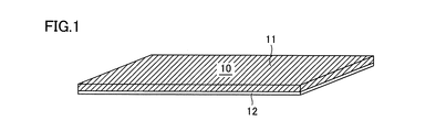
- FIG. 1 is a perspective view schematically showing a fuse element for a protection element of the first embodiment.
- the fuse element 10 is a plate-like body, and is composed of a plate-like base material 11 and a covering material 12 covering one surface of the base material 11.
- the thickness of the fuse element 10 is preferably 64 ⁇ m to 300 ⁇ m, and more preferably 80 ⁇ m to 110 ⁇ m from the viewpoint of reducing the size and thickness of the circuit protection element to be mounted.
- FIG. 2 is a perspective view schematically showing a fuse element for a protection element of the second embodiment.
- the fuse element 15 is a plate-like body, and is composed of a plate-like base material 11 and a covering material 12 covering both surfaces of the base material 11.
- the thickness of the fuse element 15 is preferably 64 ⁇ m to 300 ⁇ m, and more preferably 80 ⁇ m to 110 ⁇ m from the viewpoint of reducing the size and thickness of the circuit protection element to be mounted.
- the thickness of the covering material 12 in the fuse element 15 is preferably 1% or more and 20% or less of the thickness of the fuse element 15, for 5% or more and 15% or less, for the same reason as the first embodiment. It is further preferred that
- the fuse element 15 does not have the directionality of the front and back by providing the covering material 12 on the upper and lower surfaces of the base material 11, and erroneous mounting of the fuse element can be prevented in the process of assembling the circuit protection element.
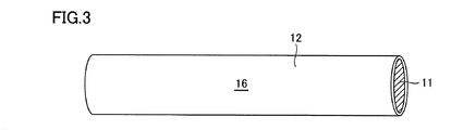
- FIG. 3 is a perspective view schematically showing a fuse element for a protection element according to a third embodiment.
- the fuse element 16 is a rod-like body, and is composed of a rod-like base material 11 and a covering material 12 covering the outer peripheral surface of the base material 11.
- the diameter of the fuse element 30 is preferably 64 to 300 ⁇ m, and more preferably 80 ⁇ m to 110 ⁇ m, from the viewpoint of reducing the size and thickness of the circuit protection element to be mounted.
- the thickness of the covering material 12 in the fuse element 30 is preferably 1% or more and 20% or less of the diameter of the fuse element 30, and is 5% or more and 15% or less for the same reason as the first embodiment. Is preferred.
- the rod-like fuse element 16 may be further rolled into a plate shape. Further, even when the diameter of the fuse element exceeds 300 ⁇ m, the rod-like fuse element 30 is formed so that the thickness of the covering material 12 is 1% or more and 20% or less with respect to the diameter of the fuse element. It can be rolled into a plate and used.
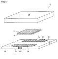
- FIG. 4 is an exploded perspective view showing the configuration of the circuit protection element of the fourth embodiment.
- the circuit protection element 20 shown in FIG. 4 includes an insulating substrate 23, a pattern electrode 24 provided on the surface of the insulating substrate 23, and a fuse element 10 joined to the pattern electrode 24 and electrically connected to the pattern electrode 24; And a cap-like lid 26 covering the element 10.
- the fuse element 10 of the first embodiment shown in FIG. 1 is used as the fuse element 10 is shown, the present invention is not limited to this, and the second or the third shown in FIG.
- the fuse elements 15 and 16 of the third embodiment can also be used.
- the insulating substrate 23 is made of a heat-resistant insulating substrate, such as a glass epoxy substrate, a BT (Bismalemide Triazine) substrate, a Teflon (registered trademark) substrate, a ceramic substrate, a glass substrate, or the like.
- the thickness of the insulating substrate 23 is, for example, 0.20 mm or more and 0.40 mm or less.
- the pattern electrode 24 is formed on the surface of the insulating substrate 23 in an arbitrary pattern, and is connected to an external circuit through terminals 27 a and 27 b provided in half through holes formed on the side surfaces of the insulating substrate 23.
- the pattern electrode 24 is for supplying a current to the fuse element 10, and is formed to be electrically open when the fuse element 10 is melted.
- the pattern electrode 24 is, for example, a metal material such as tungsten, molybdenum, nickel, copper, silver, gold or aluminum, or an alloy thereof, or a composite material in which a plurality of materials among these materials are mixed, or a material thereof.
- the cap-like lid body 26 is only required to cover the insulating substrate 23 and the fuse element 25 from above to maintain a desired space, and the shape and material are not limited. For example, dome-like resin film material, plastic material, ceramic material etc. Become.
- the circuit protection element of the present invention is incorporated in an external circuit and used. When an abnormality occurs in the external circuit and the temperature of the external circuit rises, the fuse element is melted and the operation of the external circuit is urgently stopped due to the abnormal temperature.
- the heating means applied in the bonding step (St20) is not particularly limited, and any means capable of heating the fuse element 10 placed on the insulating substrate 23 to be in contact with the pattern electrode 24 to the heating peak temperature Any method or apparatus may be used. For example, heating using a high temperature batch furnace, heating using a hot plate, heating using a reflow furnace, and the like can be suitably used.
- the fuse element 10 can be fused due to the temperature rise of the heating resistor 38.
- the conductive pattern 39 is also provided on the surface of the insulating substrate 33 so as to be in contact with the fuse element 10, so that the temperature of the heating resistor 38 can be conducted to the fuse element 10 with high efficiency.
- a configuration is adopted in which the pattern electrodes 34 or the conductive patterns 39 formed on the front and back surfaces are electrically connected via the terminals 37a, 37b, 39a, 39b provided in the half through holes.
- a conductor through hole penetrating the insulating substrate 33 or a surface wiring with a flat electrode pattern may be employed.
- a conductive pattern 49 and a heating resistor 48 are provided so as to be electrically connected to the conductive pattern 49.
- the fuse element 10 is bonded to the pattern electrode 44, it comes into contact with the resistance heating element 48.
- 6 shows the case where the fuse element 10 of the first embodiment shown in FIG. 1 is used as the fuse element 10, the present invention is not limited to this.
- the fuse elements 15 and 16 of the second or third embodiment shown can also be used.
- the circuit protection element 40 of the sixth embodiment differs from the circuit protection element 30 of the fifth embodiment only in that the heating resistor 48 is provided on the surface of the insulating substrate.
- Example 1 Fuse Element for Protection Element
- the fuse element 10 for a protection element of Example 1 has the configuration shown in FIG. 1 and is a 90 ⁇ m-thick plate made of 87 Pb-13 Sn alloy (first fusible metal) having a melting point of 280 to 290 ° C. -Shaped base material 11 and a covering material 12 with a thickness of 10 ⁇ m made of Sn-3Ag-0.5Cu alloy (second fusible metal) having a melting point of 220 ° C. Be done.
- the fuse element 15 for a protection element of Example 2 has the configuration shown in FIG. 2 and is a 90 ⁇ m-thick plate made of 87 Pb-13 Sn alloy (first fusible metal) having a melting point of 280 to 290 ° C. -Layer composite metal material in which the covering material 12 with a thickness of 5 ⁇ m made of Sn-0.7Cu alloy (second fusible metal) having a melting point of 227 ° C. is provided on the upper and lower surfaces of the base material 11 by electroplating. It consists of
- Example 3 Fuse Element for Protective Element
- the fuse element 16 for a protection element of Example 3 has the configuration shown in FIG. 3 and has a rod-like base with a diameter of 280 ⁇ m made of 87 Pb-13 Sn alloy (first fusible metal) having a melting point of 280-290 ° C. 10 m thick covering material 12 made of Sn-3.5Ag alloy (second fusible metal) having a melting point of 221 ° C. on the outer peripheral surface of the material 11, and it is made of a composite metal material Be done.
- Examples 4-1, 4-2, and 4-3 Circuit Protection Elements
- the circuit protection elements of Examples 4-1, 4-2, and 4-3 use the fuse elements for the protection elements of Examples 1 to 3, respectively, instead of the fuse element 10 of the circuit protection element 20 shown in FIG.
- the circuit protection element was formed by bonding to the pattern electrode 24.
- an insulating substrate of alumina ceramic was used as the insulating substrate 23, and an Ag alloy pattern electrode was used as the pattern electrode 24.
- Example 4-1 a flux for melting is applied to the joined fuse element, and the fuse element on the insulating substrate 23 is covered with a cap-like lid 26 made of heat-resistant plastic, and the cap-like lid 26 and the insulating substrate 23 are epoxy resin
- the circuit protection elements of Example 4-1, Example 4-2, and Example 4-3 were fixed.
- Examples 5-1, 5-2 and 5-3 Circuit Protection Elements
- the circuit protection elements of Examples 5-1, 5-2, and 5-3 use the fuse elements for the protection elements of Examples 1 to 3, respectively, instead of the fuse element 10 of the circuit protection element 30 shown in FIG.
- the circuit protection element was formed by bonding to the pattern electrode 34.
- an insulating substrate of alumina ceramic was used as the insulating substrate 33, and an Ag alloy pattern electrode was used as the pattern electrode 34.
- a heating resistor 38 was provided on the back surface of the insulating substrate 33. The surface of the heat generating resistor 38 was over glazed with a glass material.
- a flux for bonding is previously applied to the pattern electrode 34, and the fuse element is placed in contact with it, and the temperature profile is heated at a residual heat temperature of 100 to 180 ° C and a residence time of 60 seconds at 220 ° C or more for 60 seconds.
- the fuse element was collectively joined to the pattern electrode 34 by melting the second fusible metal constituting the covering material 12 through a reflow furnace set at a temperature of 230 ° C. and a residence time of 5 seconds.
- Example 5-1 Example 5-2, and Example 5-3 were fixed.
- Examples 6-1, 6-2, 6-3 Circuit Protection Elements
- the circuit protection elements of Examples 6-1, 6-2, and 6-3 use the fuse elements for the protection elements of Examples 1 to 3 in place of the fuse element 10 of the circuit protection element 40 shown in FIG.
- the circuit protection element was formed by bonding to the pattern electrode 44.
- an insulating substrate of alumina ceramic was used as the insulating substrate 43, and an Ag alloy pattern electrode was used as the pattern electrode 44.
- a heating resistor 48 is provided in advance. The surface of the heat generating resistor 38 was over glazed with a glass material.
- a bonding flux is applied in advance to the pattern electrode 44, and the fuse element is placed in contact here, and the temperature profile has a residual heat temperature of 100 to 180 ° C., residence time of 60 seconds, heating peak temperature of 220 ° C.
- the fuse element is collectively joined to the pattern electrode 44 by melting the second fusible metal constituting the covering material 12 through a reflow furnace set at 230 ° C. and a residence time of 5 seconds. Thereafter, a flux for melting is applied to the joined fuse element, the fuse element on the insulating substrate 43 is covered with a cap-like lid 46 made of liquid crystal polymer, and the cap-like lid 46 and the insulating substrate 43 are epoxy resin
- the circuit protection elements of Example 6-1, Example 6-2, and Example 6-3 were fixed.
- Comparative Example 1 Circuit Protection Element
- the circuit protection element of Comparative Example 1 is joined to the pattern electrode 34 by using a fuse element consisting of only 87Pb-13Sn alloy plate with a thickness of 100 ⁇ m instead of the fuse element 10 of the circuit protection element 30 shown in FIG. A circuit protection element was formed.
- the bonding to the pattern electrode 34 was performed using a laser welder.
- the circuit protection element of Example 5-1 shows a smaller value of the internal resistance value as compared with Comparative Example 1, and can reduce the power loss.
- the circuit protection element of Example 5-1 has the operation time shortened and the operation performance improved as compared with Comparative Example 1. It is considered that this is because the thermal conductivity is improved by increasing the bonding area.
Landscapes
- Engineering & Computer Science (AREA)
- Manufacturing & Machinery (AREA)
- Chemical & Material Sciences (AREA)
- Combustion & Propulsion (AREA)
- Power Engineering (AREA)
- Physics & Mathematics (AREA)
- Thermal Sciences (AREA)
- Fuses (AREA)
Priority Applications (3)
| Application Number | Priority Date | Filing Date | Title |
|---|---|---|---|
| CN201380025520.1A CN104303255B (zh) | 2012-05-17 | 2013-04-24 | 用于保护器件的熔断器元件及包括该元件的电路保护器件 |
| US14/400,419 US20150130585A1 (en) | 2012-05-17 | 2013-04-24 | Fuse Element for Protection Device and Circuit Protection Device Including the Same |
| KR1020147034531A KR101886478B1 (ko) | 2012-05-17 | 2013-04-24 | 보호 소자용 퓨즈 소자 및 그것을 이용한 회로 보호 소자 |
Applications Claiming Priority (2)
| Application Number | Priority Date | Filing Date | Title |
|---|---|---|---|
| JP2012-113369 | 2012-05-17 | ||
| JP2012113369A JP5896412B2 (ja) | 2012-05-17 | 2012-05-17 | 保護素子用ヒューズ素子およびそれを利用した回路保護素子 |
Publications (1)
| Publication Number | Publication Date |
|---|---|
| WO2013172160A1 true WO2013172160A1 (ja) | 2013-11-21 |
Family
ID=49583574
Family Applications (1)
| Application Number | Title | Priority Date | Filing Date |
|---|---|---|---|
| PCT/JP2013/061985 WO2013172160A1 (ja) | 2012-05-17 | 2013-04-24 | 保護素子用ヒューズ素子およびそれを用いた回路保護素子 |
Country Status (6)
Cited By (3)
| Publication number | Priority date | Publication date | Assignee | Title |
|---|---|---|---|---|
| CN105900207A (zh) * | 2014-01-20 | 2016-08-24 | 迪睿合株式会社 | 开关元件、开关电路及警报电路 |
| JP2020057492A (ja) * | 2018-10-01 | 2020-04-09 | ショット日本株式会社 | 保護素子 |
| CN114388317A (zh) * | 2020-10-16 | 2022-04-22 | 功得电子工业股份有限公司 | 保护元件及其制作方法 |
Families Citing this family (16)
| Publication number | Priority date | Publication date | Assignee | Title |
|---|---|---|---|---|
| JP6214318B2 (ja) * | 2013-10-09 | 2017-10-18 | デクセリアルズ株式会社 | 電流ヒューズ |
| JP6203136B2 (ja) * | 2014-06-27 | 2017-09-27 | エヌイーシー ショット コンポーネンツ株式会社 | 保護素子およびその製造方法、ならびに保護素子用消散性フラックス |
| CN105576598B (zh) * | 2015-02-17 | 2019-02-15 | 上海长园维安电子线路保护有限公司 | 一种薄型自控制型保护器及其制造方法 |
| US10032583B2 (en) * | 2016-02-17 | 2018-07-24 | Dexerials Corporation | Protective circuit substrate |
| JP6423384B2 (ja) * | 2016-04-06 | 2018-11-14 | ショット日本株式会社 | 保護素子 |
| JP6160788B1 (ja) | 2017-01-13 | 2017-07-12 | 千住金属工業株式会社 | フラックス |
| JP6433527B2 (ja) * | 2017-03-16 | 2018-12-05 | ショット日本株式会社 | 消散性フラックスおよびそれを用いた保護素子の製造方法 |
| US10446345B2 (en) * | 2018-01-09 | 2019-10-15 | Littelfuse, Inc. | Reflowable thermal fuse |
| JP7231527B2 (ja) | 2018-12-28 | 2023-03-01 | ショット日本株式会社 | 保護素子用ヒューズ素子およびそれを利用した保護素子 |
| WO2020138325A1 (ja) * | 2018-12-28 | 2020-07-02 | ショット日本株式会社 | ヒューズ素子および保護素子 |
| CN113284777A (zh) * | 2020-02-19 | 2021-08-20 | 功得电子工业股份有限公司 | 具有金属线型导电熔丝的芯片型保险丝及其制造方法 |
| JP7349954B2 (ja) * | 2020-04-13 | 2023-09-25 | ショット日本株式会社 | 保護素子 |
| KR102227864B1 (ko) * | 2020-11-27 | 2021-03-15 | 주식회사 인세코 | 이차전지용 보호소자 및 이를 포함하는 배터리 팩 |
| CN113937606A (zh) * | 2021-10-14 | 2022-01-14 | 浙江水晶光电科技股份有限公司 | 一种电路保护元件及其制备方法 |
| JP2023127740A (ja) * | 2022-03-02 | 2023-09-14 | デクセリアルズ株式会社 | 保護素子 |
| CN116815007B (zh) * | 2023-06-29 | 2025-08-19 | 云南贵金属实验室有限公司 | 一种高压熔断器用多条银铜侧向复合带材及其制备方法 |
Citations (2)
| Publication number | Priority date | Publication date | Assignee | Title |
|---|---|---|---|---|
| JPH02144821A (ja) * | 1988-11-25 | 1990-06-04 | Fujikura Ltd | ヒューズ形成方法 |
| JP2009170698A (ja) * | 2008-01-17 | 2009-07-30 | Toyota Motor Corp | 表面実装部品のはんだ付け装置および方法 |
Family Cites Families (16)
| Publication number | Priority date | Publication date | Assignee | Title |
|---|---|---|---|---|
| US2144821A (en) * | 1936-11-09 | 1939-01-24 | Fmc Corp | Shook selector for box-making machines |
| US2911504A (en) * | 1958-05-15 | 1959-11-03 | Sigmund Cohn Corp | Fuse member and method of making the same |
| US4320374A (en) * | 1979-03-21 | 1982-03-16 | Kearney-National (Canada) Limited | Electric fuses employing composite aluminum and cadmium fuse elements |
| JPH0547294A (ja) * | 1990-10-18 | 1993-02-26 | Sumitomo Electric Ind Ltd | ヒユーズ用導体 |
| EP0481493B1 (en) * | 1990-10-18 | 1996-02-07 | Sumitomo Electric Industries, Limited | Fuse Conductor |
| CN100376704C (zh) * | 2003-05-29 | 2008-03-26 | 松下电器产业株式会社 | 温度保险丝用元件、温度保险丝及使用了温度保险丝的电池 |
| DE102008003659A1 (de) * | 2007-03-26 | 2008-10-02 | Robert Bosch Gmbh | Schmelzsicherung zur Unterbrechung eines spannungs- und/oder stromführenden Leiters im thermischen Fehlerfall und Verfahren zur Herstellung der Schmelzsicherung |
| DE102007014334A1 (de) * | 2007-03-26 | 2008-10-02 | Robert Bosch Gmbh | Schmelzlegierungselement, Thermosicherung mit einem Schmelzlegierungselement sowie Verfahren zum Herstellen einer Thermosicherung |
| JP2009032567A (ja) * | 2007-07-27 | 2009-02-12 | Metawater Co Ltd | ヒューズ |
| JP4573865B2 (ja) | 2007-12-11 | 2010-11-04 | エヌイーシー ショット コンポーネンツ株式会社 | 温度ヒュ−ズを用いた保護装置 |
| TW200929310A (en) * | 2007-12-21 | 2009-07-01 | Chun-Chang Yen | Surface Mounted Technology type thin film fuse structure and the manufacturing method thereof |
| JP5117917B2 (ja) * | 2008-04-21 | 2013-01-16 | デクセリアルズ株式会社 | 保護素子及びその製造方法 |
| CN101447370B (zh) * | 2008-11-25 | 2010-08-25 | 南京萨特科技发展有限公司 | 一种高可靠性片式保险丝的制备方法 |
| JP5305523B2 (ja) | 2009-07-31 | 2013-10-02 | エヌイーシー ショット コンポーネンツ株式会社 | 保護素子 |
| US8976001B2 (en) * | 2010-11-08 | 2015-03-10 | Cyntec Co., Ltd. | Protective device |
| US20120194958A1 (en) * | 2011-02-02 | 2012-08-02 | Matthiesen Martyn A | Three-Function Reflowable Circuit Protection Device |
-
2012
- 2012-05-17 JP JP2012113369A patent/JP5896412B2/ja active Active
-
2013
- 2013-04-24 WO PCT/JP2013/061985 patent/WO2013172160A1/ja active Application Filing
- 2013-04-24 KR KR1020147034531A patent/KR101886478B1/ko active Active
- 2013-04-24 CN CN201380025520.1A patent/CN104303255B/zh active Active
- 2013-04-24 US US14/400,419 patent/US20150130585A1/en not_active Abandoned
- 2013-04-29 TW TW102115199A patent/TWI557765B/zh active
Patent Citations (2)
| Publication number | Priority date | Publication date | Assignee | Title |
|---|---|---|---|---|
| JPH02144821A (ja) * | 1988-11-25 | 1990-06-04 | Fujikura Ltd | ヒューズ形成方法 |
| JP2009170698A (ja) * | 2008-01-17 | 2009-07-30 | Toyota Motor Corp | 表面実装部品のはんだ付け装置および方法 |
Cited By (9)
| Publication number | Priority date | Publication date | Assignee | Title |
|---|---|---|---|---|
| CN105900207A (zh) * | 2014-01-20 | 2016-08-24 | 迪睿合株式会社 | 开关元件、开关电路及警报电路 |
| TWI655662B (zh) * | 2014-01-20 | 2019-04-01 | 日商迪睿合股份有限公司 | Switching element, switching circuit, and alarm circuit |
| CN105900207B (zh) * | 2014-01-20 | 2019-09-06 | 迪睿合株式会社 | 开关元件、开关电路及警报电路 |
| JP2020057492A (ja) * | 2018-10-01 | 2020-04-09 | ショット日本株式会社 | 保護素子 |
| KR20210035313A (ko) | 2018-10-01 | 2021-03-31 | 쇼트 니혼 가부시키가이샤 | 보호 소자 |
| DE112019004929T5 (de) | 2018-10-01 | 2021-08-12 | Schott Japan Corporation | Schutzelement |
| JP7154090B2 (ja) | 2018-10-01 | 2022-10-17 | ショット日本株式会社 | 保護素子 |
| US11817694B2 (en) | 2018-10-01 | 2023-11-14 | Schott Japan Corporation | Protection element and protection circuit for a battery |
| CN114388317A (zh) * | 2020-10-16 | 2022-04-22 | 功得电子工业股份有限公司 | 保护元件及其制作方法 |
Also Published As
| Publication number | Publication date |
|---|---|
| JP2013239405A (ja) | 2013-11-28 |
| KR20150009989A (ko) | 2015-01-27 |
| CN104303255A (zh) | 2015-01-21 |
| CN104303255B (zh) | 2016-10-26 |
| JP5896412B2 (ja) | 2016-03-30 |
| TW201409517A (zh) | 2014-03-01 |
| US20150130585A1 (en) | 2015-05-14 |
| TWI557765B (zh) | 2016-11-11 |
| KR101886478B1 (ko) | 2018-08-07 |
Similar Documents
| Publication | Publication Date | Title |
|---|---|---|
| WO2013172160A1 (ja) | 保護素子用ヒューズ素子およびそれを用いた回路保護素子 | |
| US8767368B2 (en) | Protective element and method for producing the same | |
| US11640892B2 (en) | Fuse element and protective element | |
| CN215869263U (zh) | 保护元件及其电路保护装置 | |
| JP2015079608A (ja) | 保護素子用ヒューズエレメント材およびそれを利用した回路保護素子 | |
| JP7050019B2 (ja) | 保護素子 | |
| TWI676202B (zh) | 保護元件 | |
| JP6423384B2 (ja) | 保護素子 | |
| JP6711704B2 (ja) | バイパス電極付き保護素子 | |
| JP2000348583A (ja) | 合金型温度ヒュ−ズ | |
| CN221304566U (zh) | 保护组件 | |
| CN222071854U (zh) | 熔丝组件 | |
| JP7040886B2 (ja) | 保護素子 | |
| KR20250130753A (ko) | 퓨즈 합금 및 보호 소자 | |
| WO2020138325A1 (ja) | ヒューズ素子および保護素子 | |
| CN109788643A (zh) | 铝基可焊接的触头 | |
| KR20230034380A (ko) | 퓨즈 엘리먼트, 퓨즈 소자 및 보호 소자 | |
| JPH02244530A (ja) | 基板型温度ヒューズ及びその製造方法 | |
| JP2020126821A (ja) | 保護素子 | |
| JP2023126322A (ja) | 回路モジュール | |
| TW202414484A (zh) | 保護元件 | |
| JP2000182493A (ja) | 回路用保護素子 |
Legal Events
| Date | Code | Title | Description |
|---|---|---|---|
| 121 | Ep: the epo has been informed by wipo that ep was designated in this application |
Ref document number: 13789981 Country of ref document: EP Kind code of ref document: A1 |
|
| WWE | Wipo information: entry into national phase |
Ref document number: 14400419 Country of ref document: US |
|
| NENP | Non-entry into the national phase |
Ref country code: DE |
|
| ENP | Entry into the national phase |
Ref document number: 20147034531 Country of ref document: KR Kind code of ref document: A |
|
| 122 | Ep: pct application non-entry in european phase |
Ref document number: 13789981 Country of ref document: EP Kind code of ref document: A1 |