WO2013172160A1 - Fuse element for protection element, and circuit protection element using fuse element for protection element - Google Patents
Fuse element for protection element, and circuit protection element using fuse element for protection element Download PDFInfo
- Publication number
- WO2013172160A1 WO2013172160A1 PCT/JP2013/061985 JP2013061985W WO2013172160A1 WO 2013172160 A1 WO2013172160 A1 WO 2013172160A1 JP 2013061985 W JP2013061985 W JP 2013061985W WO 2013172160 A1 WO2013172160 A1 WO 2013172160A1
- Authority
- WO
- WIPO (PCT)
- Prior art keywords
- alloy
- fuse element
- pattern electrode
- protection element
- fuse
- Prior art date
Links
Images


Classifications
-
- H—ELECTRICITY
- H01—ELECTRIC ELEMENTS
- H01H—ELECTRIC SWITCHES; RELAYS; SELECTORS; EMERGENCY PROTECTIVE DEVICES
- H01H37/00—Thermally-actuated switches
- H01H37/02—Details
- H01H37/32—Thermally-sensitive members
-
- H—ELECTRICITY
- H01—ELECTRIC ELEMENTS
- H01H—ELECTRIC SWITCHES; RELAYS; SELECTORS; EMERGENCY PROTECTIVE DEVICES
- H01H37/00—Thermally-actuated switches
- H01H37/74—Switches in which only the opening movement or only the closing movement of a contact is effected by heating or cooling
- H01H37/76—Contact member actuated by melting of fusible material, actuated due to burning of combustible material or due to explosion of explosive material
- H01H37/761—Contact member actuated by melting of fusible material, actuated due to burning of combustible material or due to explosion of explosive material with a fusible element forming part of the switched circuit
-
- H—ELECTRICITY
- H01—ELECTRIC ELEMENTS
- H01H—ELECTRIC SWITCHES; RELAYS; SELECTORS; EMERGENCY PROTECTIVE DEVICES
- H01H37/00—Thermally-actuated switches
- H01H37/02—Details
- H01H37/04—Bases; Housings; Mountings
-
- H—ELECTRICITY
- H01—ELECTRIC ELEMENTS
- H01H—ELECTRIC SWITCHES; RELAYS; SELECTORS; EMERGENCY PROTECTIVE DEVICES
- H01H37/00—Thermally-actuated switches
- H01H37/02—Details
- H01H37/64—Contacts
-
- H—ELECTRICITY
- H01—ELECTRIC ELEMENTS
- H01H—ELECTRIC SWITCHES; RELAYS; SELECTORS; EMERGENCY PROTECTIVE DEVICES
- H01H69/00—Apparatus or processes for the manufacture of emergency protective devices
- H01H69/02—Manufacture of fuses
-
- H—ELECTRICITY
- H01—ELECTRIC ELEMENTS
- H01H—ELECTRIC SWITCHES; RELAYS; SELECTORS; EMERGENCY PROTECTIVE DEVICES
- H01H69/00—Apparatus or processes for the manufacture of emergency protective devices
- H01H69/02—Manufacture of fuses
- H01H69/022—Manufacture of fuses of printed circuit fuses
-
- H—ELECTRICITY
- H01—ELECTRIC ELEMENTS
- H01H—ELECTRIC SWITCHES; RELAYS; SELECTORS; EMERGENCY PROTECTIVE DEVICES
- H01H85/00—Protective devices in which the current flows through a part of fusible material and this current is interrupted by displacement of the fusible material when this current becomes excessive
- H01H85/02—Details
- H01H85/0241—Structural association of a fuse and another component or apparatus
-
- H—ELECTRICITY
- H01—ELECTRIC ELEMENTS
- H01H—ELECTRIC SWITCHES; RELAYS; SELECTORS; EMERGENCY PROTECTIVE DEVICES
- H01H37/00—Thermally-actuated switches
- H01H37/02—Details
- H01H37/04—Bases; Housings; Mountings
- H01H2037/046—Bases; Housings; Mountings being soldered on the printed circuit to be protected
-
- H—ELECTRICITY
- H01—ELECTRIC ELEMENTS
- H01H—ELECTRIC SWITCHES; RELAYS; SELECTORS; EMERGENCY PROTECTIVE DEVICES
- H01H85/00—Protective devices in which the current flows through a part of fusible material and this current is interrupted by displacement of the fusible material when this current becomes excessive
- H01H85/02—Details
- H01H85/0241—Structural association of a fuse and another component or apparatus
- H01H2085/0275—Structural association with a printed circuit board
-
- H—ELECTRICITY
- H01—ELECTRIC ELEMENTS
- H01H—ELECTRIC SWITCHES; RELAYS; SELECTORS; EMERGENCY PROTECTIVE DEVICES
- H01H85/00—Protective devices in which the current flows through a part of fusible material and this current is interrupted by displacement of the fusible material when this current becomes excessive
- H01H85/48—Protective devices wherein the fuse is carried or held directly by the base
-
- Y—GENERAL TAGGING OF NEW TECHNOLOGICAL DEVELOPMENTS; GENERAL TAGGING OF CROSS-SECTIONAL TECHNOLOGIES SPANNING OVER SEVERAL SECTIONS OF THE IPC; TECHNICAL SUBJECTS COVERED BY FORMER USPC CROSS-REFERENCE ART COLLECTIONS [XRACs] AND DIGESTS
- Y10—TECHNICAL SUBJECTS COVERED BY FORMER USPC
- Y10T—TECHNICAL SUBJECTS COVERED BY FORMER US CLASSIFICATION
- Y10T29/00—Metal working
- Y10T29/49—Method of mechanical manufacture
- Y10T29/49002—Electrical device making
- Y10T29/49107—Fuse making
Definitions
- a chip protection element of a surface mount component is suitably used for a protection circuit of a secondary battery pack.
- These chip protection elements include non-restoring protection elements that detect excessive heat generation caused by the overcurrent of the protected equipment, or respond to abnormal overheating of the ambient temperature, and activate the fuse and shut off the electrical circuit under predetermined conditions. is there.
- the protection circuit detects an abnormality generated in the device, the protection element causes the resistance element to generate heat by the signal current to melt the fuse element made of a fusible alloy material.
- the fuse element has a base material and a coating material that covers at least a part of the surface of the base material,
- the base material is made of a first fusible metal whose melting point is higher than the heating temperature
- the covering material is made of a second fusible metal whose melting point is lower than the heating temperature
- the circuit protection element wherein the heating temperature is 183 ° C. or more and less than 280 ° C.
- the second fusible metal is Sn-Ag alloy, Sn-Bi alloy, Sn-Cu alloy, Sn-Zn alloy, Sn-Sb alloy, Sn-Ag-Bi alloy, Sn-Ag-Cu Alloy, Sn—Ag—In alloy, Sn—Zn—Al alloy, Sn—Zn—Bi alloy, or an alloy containing at least one metal element of Au, Ni, Ge, Ga in addition to these alloys [7 ]
- the circuit protection element in any one of-[9].
- the fuse element of the present invention is heated to a predetermined heating temperature (hereinafter also referred to as "heating peak temperature") and joined to the protective element.
- the base material is made of a first fusible metal whose melting point is higher than the heating peak temperature
- the covering material is made of a second fusible metal whose melting point is lower than the heating peak temperature.
- the second element of the cover material is formed by heating the fuse element or the fuse element and the protection element while the cover material of the fuse element is in contact with the connection portion of the protection element.
- the fusible metal melts and the fuse element and the protection element are joined.
- the heating peak temperature is preferably 183 ° C. or more and less than 280 ° C., and more preferably 219 ° C. or more and less than 227 ° C.
- the metal that can be used as the first fusible metal differs depending on the heating peak temperature, but a 20Sn-80Au alloy, a 55Sn-45Sb alloy, a Pb-Sn alloy containing 80 mass% or more of Pb, etc. are preferable.
- the number added before each element symbol represents the blending ratio (% by weight) of the alloy.
- the metal that can be used as the second fusible metal differs depending on the heating peak temperature, but Sn-Ag alloy, Sn-Bi alloy, Sn-Cu alloy, Sn-Zn alloy, Sn-Sb alloy, Sn-Ag- Bi alloy, Sn-Ag-Cu alloy, Sn-Ag-In alloy, Sn-Zn-Al alloy, Sn-Zn-Bi alloy, or alloys of these are further added with at least one metal element of Au, Ni, Ge, Ga Alloys and the like are preferable.
- the method for providing the covering material on the surface of the base material is not particularly limited as long as the covering material is fixed to the surface of the base material.
- the covering material can be fixed to the surface of the base material by a method such as cladding, plating, melt coating, pressure bonding, adhesion with a fusible resin such as rosin.
- the base material may be either a single layer or multiple layers, but preferably comprises a single layer.
- the covering material may be either a single layer or multiple layers, but preferably comprises a single layer.
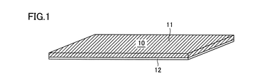
- FIG. 1 is a perspective view schematically showing a fuse element for a protection element of the first embodiment.
- the fuse element 10 is a plate-like body, and is composed of a plate-like base material 11 and a covering material 12 covering one surface of the base material 11.
- the thickness of the fuse element 10 is preferably 64 ⁇ m to 300 ⁇ m, and more preferably 80 ⁇ m to 110 ⁇ m from the viewpoint of reducing the size and thickness of the circuit protection element to be mounted.
- FIG. 2 is a perspective view schematically showing a fuse element for a protection element of the second embodiment.
- the fuse element 15 is a plate-like body, and is composed of a plate-like base material 11 and a covering material 12 covering both surfaces of the base material 11.
- the thickness of the fuse element 15 is preferably 64 ⁇ m to 300 ⁇ m, and more preferably 80 ⁇ m to 110 ⁇ m from the viewpoint of reducing the size and thickness of the circuit protection element to be mounted.
- the thickness of the covering material 12 in the fuse element 15 is preferably 1% or more and 20% or less of the thickness of the fuse element 15, for 5% or more and 15% or less, for the same reason as the first embodiment. It is further preferred that
- the fuse element 15 does not have the directionality of the front and back by providing the covering material 12 on the upper and lower surfaces of the base material 11, and erroneous mounting of the fuse element can be prevented in the process of assembling the circuit protection element.
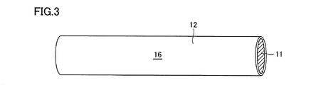
- FIG. 3 is a perspective view schematically showing a fuse element for a protection element according to a third embodiment.
- the fuse element 16 is a rod-like body, and is composed of a rod-like base material 11 and a covering material 12 covering the outer peripheral surface of the base material 11.
- the diameter of the fuse element 30 is preferably 64 to 300 ⁇ m, and more preferably 80 ⁇ m to 110 ⁇ m, from the viewpoint of reducing the size and thickness of the circuit protection element to be mounted.
- the thickness of the covering material 12 in the fuse element 30 is preferably 1% or more and 20% or less of the diameter of the fuse element 30, and is 5% or more and 15% or less for the same reason as the first embodiment. Is preferred.
- the rod-like fuse element 16 may be further rolled into a plate shape. Further, even when the diameter of the fuse element exceeds 300 ⁇ m, the rod-like fuse element 30 is formed so that the thickness of the covering material 12 is 1% or more and 20% or less with respect to the diameter of the fuse element. It can be rolled into a plate and used.
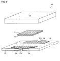
- FIG. 4 is an exploded perspective view showing the configuration of the circuit protection element of the fourth embodiment.
- the circuit protection element 20 shown in FIG. 4 includes an insulating substrate 23, a pattern electrode 24 provided on the surface of the insulating substrate 23, and a fuse element 10 joined to the pattern electrode 24 and electrically connected to the pattern electrode 24; And a cap-like lid 26 covering the element 10.
- the fuse element 10 of the first embodiment shown in FIG. 1 is used as the fuse element 10 is shown, the present invention is not limited to this, and the second or the third shown in FIG.
- the fuse elements 15 and 16 of the third embodiment can also be used.
- the insulating substrate 23 is made of a heat-resistant insulating substrate, such as a glass epoxy substrate, a BT (Bismalemide Triazine) substrate, a Teflon (registered trademark) substrate, a ceramic substrate, a glass substrate, or the like.
- the thickness of the insulating substrate 23 is, for example, 0.20 mm or more and 0.40 mm or less.
- the pattern electrode 24 is formed on the surface of the insulating substrate 23 in an arbitrary pattern, and is connected to an external circuit through terminals 27 a and 27 b provided in half through holes formed on the side surfaces of the insulating substrate 23.
- the pattern electrode 24 is for supplying a current to the fuse element 10, and is formed to be electrically open when the fuse element 10 is melted.
- the pattern electrode 24 is, for example, a metal material such as tungsten, molybdenum, nickel, copper, silver, gold or aluminum, or an alloy thereof, or a composite material in which a plurality of materials among these materials are mixed, or a material thereof.
- the cap-like lid body 26 is only required to cover the insulating substrate 23 and the fuse element 25 from above to maintain a desired space, and the shape and material are not limited. For example, dome-like resin film material, plastic material, ceramic material etc. Become.
- the circuit protection element of the present invention is incorporated in an external circuit and used. When an abnormality occurs in the external circuit and the temperature of the external circuit rises, the fuse element is melted and the operation of the external circuit is urgently stopped due to the abnormal temperature.
- the heating means applied in the bonding step (St20) is not particularly limited, and any means capable of heating the fuse element 10 placed on the insulating substrate 23 to be in contact with the pattern electrode 24 to the heating peak temperature Any method or apparatus may be used. For example, heating using a high temperature batch furnace, heating using a hot plate, heating using a reflow furnace, and the like can be suitably used.
- the fuse element 10 can be fused due to the temperature rise of the heating resistor 38.
- the conductive pattern 39 is also provided on the surface of the insulating substrate 33 so as to be in contact with the fuse element 10, so that the temperature of the heating resistor 38 can be conducted to the fuse element 10 with high efficiency.
- a configuration is adopted in which the pattern electrodes 34 or the conductive patterns 39 formed on the front and back surfaces are electrically connected via the terminals 37a, 37b, 39a, 39b provided in the half through holes.
- a conductor through hole penetrating the insulating substrate 33 or a surface wiring with a flat electrode pattern may be employed.
- a conductive pattern 49 and a heating resistor 48 are provided so as to be electrically connected to the conductive pattern 49.
- the fuse element 10 is bonded to the pattern electrode 44, it comes into contact with the resistance heating element 48.
- 6 shows the case where the fuse element 10 of the first embodiment shown in FIG. 1 is used as the fuse element 10, the present invention is not limited to this.
- the fuse elements 15 and 16 of the second or third embodiment shown can also be used.
- the circuit protection element 40 of the sixth embodiment differs from the circuit protection element 30 of the fifth embodiment only in that the heating resistor 48 is provided on the surface of the insulating substrate.
- Example 1 Fuse Element for Protection Element
- the fuse element 10 for a protection element of Example 1 has the configuration shown in FIG. 1 and is a 90 ⁇ m-thick plate made of 87 Pb-13 Sn alloy (first fusible metal) having a melting point of 280 to 290 ° C. -Shaped base material 11 and a covering material 12 with a thickness of 10 ⁇ m made of Sn-3Ag-0.5Cu alloy (second fusible metal) having a melting point of 220 ° C. Be done.
- the fuse element 15 for a protection element of Example 2 has the configuration shown in FIG. 2 and is a 90 ⁇ m-thick plate made of 87 Pb-13 Sn alloy (first fusible metal) having a melting point of 280 to 290 ° C. -Layer composite metal material in which the covering material 12 with a thickness of 5 ⁇ m made of Sn-0.7Cu alloy (second fusible metal) having a melting point of 227 ° C. is provided on the upper and lower surfaces of the base material 11 by electroplating. It consists of
- Example 3 Fuse Element for Protective Element
- the fuse element 16 for a protection element of Example 3 has the configuration shown in FIG. 3 and has a rod-like base with a diameter of 280 ⁇ m made of 87 Pb-13 Sn alloy (first fusible metal) having a melting point of 280-290 ° C. 10 m thick covering material 12 made of Sn-3.5Ag alloy (second fusible metal) having a melting point of 221 ° C. on the outer peripheral surface of the material 11, and it is made of a composite metal material Be done.
- Examples 4-1, 4-2, and 4-3 Circuit Protection Elements
- the circuit protection elements of Examples 4-1, 4-2, and 4-3 use the fuse elements for the protection elements of Examples 1 to 3, respectively, instead of the fuse element 10 of the circuit protection element 20 shown in FIG.
- the circuit protection element was formed by bonding to the pattern electrode 24.
- an insulating substrate of alumina ceramic was used as the insulating substrate 23, and an Ag alloy pattern electrode was used as the pattern electrode 24.
- Example 4-1 a flux for melting is applied to the joined fuse element, and the fuse element on the insulating substrate 23 is covered with a cap-like lid 26 made of heat-resistant plastic, and the cap-like lid 26 and the insulating substrate 23 are epoxy resin
- the circuit protection elements of Example 4-1, Example 4-2, and Example 4-3 were fixed.
- Examples 5-1, 5-2 and 5-3 Circuit Protection Elements
- the circuit protection elements of Examples 5-1, 5-2, and 5-3 use the fuse elements for the protection elements of Examples 1 to 3, respectively, instead of the fuse element 10 of the circuit protection element 30 shown in FIG.
- the circuit protection element was formed by bonding to the pattern electrode 34.
- an insulating substrate of alumina ceramic was used as the insulating substrate 33, and an Ag alloy pattern electrode was used as the pattern electrode 34.
- a heating resistor 38 was provided on the back surface of the insulating substrate 33. The surface of the heat generating resistor 38 was over glazed with a glass material.
- a flux for bonding is previously applied to the pattern electrode 34, and the fuse element is placed in contact with it, and the temperature profile is heated at a residual heat temperature of 100 to 180 ° C and a residence time of 60 seconds at 220 ° C or more for 60 seconds.
- the fuse element was collectively joined to the pattern electrode 34 by melting the second fusible metal constituting the covering material 12 through a reflow furnace set at a temperature of 230 ° C. and a residence time of 5 seconds.
- Example 5-1 Example 5-2, and Example 5-3 were fixed.
- Examples 6-1, 6-2, 6-3 Circuit Protection Elements
- the circuit protection elements of Examples 6-1, 6-2, and 6-3 use the fuse elements for the protection elements of Examples 1 to 3 in place of the fuse element 10 of the circuit protection element 40 shown in FIG.
- the circuit protection element was formed by bonding to the pattern electrode 44.
- an insulating substrate of alumina ceramic was used as the insulating substrate 43, and an Ag alloy pattern electrode was used as the pattern electrode 44.
- a heating resistor 48 is provided in advance. The surface of the heat generating resistor 38 was over glazed with a glass material.
- a bonding flux is applied in advance to the pattern electrode 44, and the fuse element is placed in contact here, and the temperature profile has a residual heat temperature of 100 to 180 ° C., residence time of 60 seconds, heating peak temperature of 220 ° C.
- the fuse element is collectively joined to the pattern electrode 44 by melting the second fusible metal constituting the covering material 12 through a reflow furnace set at 230 ° C. and a residence time of 5 seconds. Thereafter, a flux for melting is applied to the joined fuse element, the fuse element on the insulating substrate 43 is covered with a cap-like lid 46 made of liquid crystal polymer, and the cap-like lid 46 and the insulating substrate 43 are epoxy resin
- the circuit protection elements of Example 6-1, Example 6-2, and Example 6-3 were fixed.
- Comparative Example 1 Circuit Protection Element
- the circuit protection element of Comparative Example 1 is joined to the pattern electrode 34 by using a fuse element consisting of only 87Pb-13Sn alloy plate with a thickness of 100 ⁇ m instead of the fuse element 10 of the circuit protection element 30 shown in FIG. A circuit protection element was formed.
- the bonding to the pattern electrode 34 was performed using a laser welder.
- the circuit protection element of Example 5-1 shows a smaller value of the internal resistance value as compared with Comparative Example 1, and can reduce the power loss.
- the circuit protection element of Example 5-1 has the operation time shortened and the operation performance improved as compared with Comparative Example 1. It is considered that this is because the thermal conductivity is improved by increasing the bonding area.
Abstract
Description
[1]ベース材と、前記ベース材の少なくとも一部の表面を被覆する被覆材とを有し、所定の加熱温度まで加熱して保護素子に接合される保護素子用ヒューズ素子であって、
前記ベース材は、融点が前記加熱温度より高い第1の可融性金属からなり、
前記被覆材は、融点が前記加熱温度より低い第2の可融性金属からなる、保護素子用ヒューズ素子。 The present invention has been made to solve the above problems, and includes the following.
[1] A fuse element for a protection element, comprising a base material and a covering material for covering at least a part of the surface of the base material, which is heated to a predetermined heating temperature and joined to a protection element,
The base material is made of a first fusible metal whose melting point is higher than the heating temperature,
The fuse element for a protective element, wherein the covering material is made of a second fusible metal whose melting point is lower than the heating temperature.
前記ヒューズ素子は、ベース材と、前記ベース材の少なくとも一部の表面を被覆する被覆材とを有し、
前記ベース材は、融点が前記加熱温度より高い第1の可融性金属からなり、
前記被覆材は、融点が前記加熱温度より低い第2の可融性金属からなり、
前記加熱温度は、183℃以上280℃未満である、回路保護素子。 [7] An insulating substrate, a pattern electrode provided on the surface of the insulating substrate, and a fuse element which is heated to a predetermined heating temperature and joined to the pattern electrode and electrically connected to the pattern electrode,
The fuse element has a base material and a coating material that covers at least a part of the surface of the base material,
The base material is made of a first fusible metal whose melting point is higher than the heating temperature,
The covering material is made of a second fusible metal whose melting point is lower than the heating temperature,
The circuit protection element, wherein the heating temperature is 183 ° C. or more and less than 280 ° C.
前記パターン電極に前記ヒューズ素子の前記被覆材を接触させた状態で、前記ヒューズ素子を183℃以上280℃未満の加熱温度まで加熱し、前記パターン電極に前記ヒューズ素子を接合し電気接続する接合工程と、
前記ヒューズ素子に動作用の溶断フラックスを塗布する溶断フラックス塗布工程と、
前記ヒューズ素子をキャップ状蓋体で覆ってパッケージングするパッケージ工程と、を有し、
前記ヒューズ素子において、前記ベース材は、融点が前記接合工程における加熱温度より高い第1の可融性金属からなり、前記被覆材は、融点が前記加熱温度より低い第2の可融性金属からなる、回路保護素子の製造方法。 [12] A preparation step of preparing an insulating substrate provided with a pattern electrode on the surface, and a fuse element having a base material and a coating material covering the surface of at least a part of the base material;
A bonding step of heating the fuse element to a heating temperature of 183 ° C. or more and less than 280 ° C. in a state in which the coating material of the fuse element is in contact with the pattern electrode, bonding the fuse element to the pattern electrode and electrically connecting When,
A fusing flux applying step of applying a fusing flux for operation to the fuse element;
And packaging the fuse element with a cap-like lid.
In the fuse element, the base material is made of a first fusible metal whose melting point is higher than the heating temperature in the bonding step, and the covering material is made of a second fusible metal whose melting point is lower than the heating temperature. And a method of manufacturing a circuit protection device.
本発明のヒューズ素子は、ベース材と、ベース材の少なくとも一部の表面を被覆する被覆材とを有し、所定の加熱温度まで加熱して保護素子に接合される。ヒューズ素子の形状は限定されることはなく、例えば、板状体、棒状体等である。被覆材は、ベース材の少なくとも一部の表面を被覆するように設けられ、表面全体を被覆するように設けられていてもよい。たとえば、板状のベース材を用いて、被覆材を、ベース材一方の表面、または両方の表面に設けて、全体として板状体のヒューズ素子を構成することができる。または、棒状のベース材を用いて、被覆材を、ベース材の外周表面を被覆するように設けて、全体として棒状体のヒューズ素子を構成することができる。 [Fuse element for protection element]
The fuse element of the present invention has a base material and a covering material that covers at least a part of the surface of the base material, and is heated to a predetermined heating temperature and joined to the protection element. The shape of the fuse element is not limited and is, for example, a plate-like body, a rod-like body or the like. The covering material is provided so as to cover the surface of at least a part of the base material, and may be provided so as to cover the entire surface. For example, a plate-like base material may be used, and the covering material may be provided on one surface or both surfaces of the base material to form a plate-like fuse element as a whole. Alternatively, by using a rod-like base material, the covering material can be provided to cover the outer peripheral surface of the base material to form a rod-like fuse element as a whole.
図1は、第1の実施形態の保護素子用ヒューズ素子を模式的に表す斜視図である。図1に示すように、ヒューズ素子10は板状体であり、板状のベース材11と、ベース材11の一方の表面を被覆する被覆材12とからなる。ヒューズ素子10の厚さは、搭載する回路保護素子の小型化・薄型化の観点から、64μm~300μmであることが好ましく、80μm~110μmであることがさらに好ましい。 First Embodiment
FIG. 1 is a perspective view schematically showing a fuse element for a protection element of the first embodiment. As shown in FIG. 1, the
図2は、第2の実施形態の保護素子用ヒューズ素子を模式的に表す斜視図である。図2に示すように、ヒューズ素子15は板状体であり、板状のベース材11と、ベース材11の両方の表面を被覆する被覆材12とからなる。ヒューズ素子15の厚さは、搭載する回路保護素子の小型化・薄型化の観点から、64μm~300μmであることが好ましく、80μm~110μmであることがさらに好ましい。ヒューズ素子15中の被覆材12の厚さは、第1の実施形態と同様の理由から、ヒューズ素子15の厚さの1%以上20%以下であることが好ましく、5%以上15%以下であることがさらに好ましい。 Second Embodiment
FIG. 2 is a perspective view schematically showing a fuse element for a protection element of the second embodiment. As shown in FIG. 2, the
図3は、第3の実施形態の保護素子用ヒューズ素子を模式的に表す斜視図である。図3に示すように、ヒューズ素子16は棒状体であり、棒状のベース材11と、ベース材11の外周面を被覆する被覆材12とからなる。ヒューズ素子30の直径は、搭載する回路保護素子の小型化・薄型化の観点から、64~300μmであることが好ましく、80μm~110μmであることがさらに好ましい。ヒューズ素子30中の被覆材12の厚さは、第1の実施形態と同様の理由から、ヒューズ素子30の直径の1%以上20%以下であることが好ましく、5%以上15%以下であることが好ましい。 Third Embodiment
FIG. 3 is a perspective view schematically showing a fuse element for a protection element according to a third embodiment. As shown in FIG. 3, the
(第4の実施形態)
図4は、第4の実施形態の回路保護素子の構成を示す分解斜視図である。図4に示す回路保護素子20は、絶縁基板23と、絶縁基板23の表面に設けられたパターン電極24と、パターン電極24に接合され、パターン電極24に電気接続されたヒューズ素子10と、ヒューズ素子10の覆うキャップ状蓋体26とを備える。ヒューズ素子10としては、図1に示す第1の実施形態のヒューズ素子10が用いられている場合を示しているが、これに限定されることはなく、図2または図3に示す第2または第3の実施形態のヒューズ素子15,16を用いることもできる。 [Circuit protection element]
Fourth Embodiment
FIG. 4 is an exploded perspective view showing the configuration of the circuit protection element of the fourth embodiment. The
図5は、第5の実施形態の回路保護素子の構成を示す図である。図5(a)は上面の模式図であり、図5(b)は縦断面図であり、図5(c)は下面の模式図である。図5(a)は、図5(b)のd-d断面図に相当し、図5(b)は図5(a)または(c)のD-D断面図に相当する。図5に示す回路保護素子30は、絶縁基板33と、絶縁基板33の表面に設けられたパターン電極34と、パターン電極34に接合され、パターン電極34に電気接続されたヒューズ素子10と、ヒューズ素子10を覆うキャップ状蓋体36とを備える。また、絶縁基板33の裏面には導電パターン39と、導電パターン39に電気接続するように発熱抵抗体38が設けられている。ヒューズ素子10としては、図1に示す第1の実施形態のヒューズ素子10が用いられている場合を示しているが、これに限定されることはなく、図2または図3に示す第2または第3の実施形態のヒューズ素子15,16を用いることもできる。 Fifth Embodiment
FIG. 5 is a diagram showing the configuration of the circuit protection element of the fifth embodiment. Fig.5 (a) is a schematic diagram of an upper surface, FIG.5 (b) is a longitudinal cross-sectional view, FIG.5 (c) is a schematic diagram of a lower surface. 5 (a) corresponds to the dd cross section of FIG. 5 (b), and FIG. 5 (b) corresponds to the DD cross section of FIG. 5 (a) or (c). The
図6は、第6の実施形態の回路保護素子の構成を示す図である。図6(a)は上面の模式図であり、図6(b)は縦断面図であり、図6(c)は下面の模式図である。図6(a)は、図6(b)のd-d断面図に相当し、図6(b)は図6(a)または(c)のD-D断面図に相当する。図6に示す回路保護素子40は、絶縁基板43と、絶縁基板43の表面に設けられたパターン電極44と、パターン電極44に接合され、パターン電極44に電気接続されたヒューズ素子10と、ヒューズ素子10を覆うキャップ状蓋体46とを備える。また、絶縁基板43の表面のヒューズ素子10の下側には、導電パターン49と、導電パターン49に電気接続するように発熱抵抗体48が設けられている。ヒューズ素子10がパターン電極44に接合されると、抵抗発熱体48に接触した状態になる。図6においては、ヒューズ素子10として、図1に示す第1の実施形態のヒューズ素子10が用いられている場合を示しているが、これに限定されることはなく、図2または図3に示す第2または第3の実施形態のヒューズ素子15,16を用いることもできる。 Sixth Embodiment
FIG. 6 is a diagram showing the configuration of the circuit protection element of the sixth embodiment. 6 (a) is a schematic view of the upper surface, FIG. 6 (b) is a longitudinal sectional view, and FIG. 6 (c) is a schematic view of the lower surface. 6 (a) corresponds to the dd cross section of FIG. 6 (b), and FIG. 6 (b) corresponds to the DD cross section of FIG. 6 (a) or (c). The
実施例1の保護素子用ヒューズ素子10は、図1に示す構成を有するものであり、融点が280~290℃の87Pb-13Sn合金(第1の可融性金属)からなる厚さ90μmの板状のベース材11と、融点が220℃のSn-3Ag-0.5Cu合金(第2の可融性金属)からなる厚さ10μmの被覆材12とをクラッドにより貼り合わせた複合金属材で構成される。 Example 1: Fuse Element for Protection Element
The
実施例2の保護素子用ヒューズ素子15は、図2に示す構成を有するものであり、融点が280~290℃の87Pb-13Sn合金(第1の可融性金属)からなる厚さ90μmの板状のベース材11の上下面に、融点が227℃のSn-0.7Cu合金(第2の可融性金属)からなる厚さ5μmの被覆材12を電気めっきにより設けた三層複合金属材で構成される。 (Example 2: Fuse element for protection element)
The
実施例3の保護素子用ヒューズ素子16は、図3に示す構成を有するものであり、融点が280~290℃の87Pb-13Sn合金(第1の可融性金属)からなる直径280μmの棒状ベース材11の外周表面に、融点が221℃のSn-3.5Ag合金(第2の可融性金属)からなる厚さ10μmの被覆材12を、被覆伸線により圧着させた複合金属材で構成される。 Example 3: Fuse Element for Protective Element
The
実施例4-1、4-2、4-3の回路保護素子は、それぞれ実施例1~3の保護素子用ヒューズ素子を、図4に示す回路保護素子20のヒューズ素子10の代わりに用いて、パターン電極24に接合して回路保護素子を構成した。図4に示す回路保護素子20において、絶縁基板23としてアルミナ・セラミックスの絶縁基板を用い、パターン電極24としてAg合金パターン電極を用いた。 Examples 4-1, 4-2, and 4-3: Circuit Protection Elements
The circuit protection elements of Examples 4-1, 4-2, and 4-3 use the fuse elements for the protection elements of Examples 1 to 3, respectively, instead of the
実施例5-1、5-2、5-3の回路保護素子は、それぞれ実施例1~3の保護素子用ヒューズ素子を、図5に示す回路保護素子30のヒューズ素子10の代わりに用いて、パターン電極34に接合して回路保護素子を構成した。図5に示す回路保護素子30において、絶縁基板33としてアルミナ・セラミックスの絶縁基板を用い、パターン電極34としてAg合金パターン電極を用いた。また、絶縁基板33の裏面には、発熱抵抗体38を設けた。発熱抵抗体38の表面にはガラス材のオーバーグレーズを施した。 Examples 5-1, 5-2 and 5-3: Circuit Protection Elements
The circuit protection elements of Examples 5-1, 5-2, and 5-3 use the fuse elements for the protection elements of Examples 1 to 3, respectively, instead of the
実施例6-1、6-2、6-3の回路保護素子は、それぞれ実施例1~3の保護素子用ヒューズ素子を、図6に示す回路保護素子40のヒューズ素子10の代わりに用いて、パターン電極44に接合して回路保護素子を形成した。図6に示す回路保護素子40において、絶縁基板43としてアルミナ・セラミックスの絶縁基板を用い、パターン電極44としてAg合金パターン電極を用いた。また、絶縁基板43の表面には、予め発熱抵抗体48を設けた。発熱抵抗体38の表面にはガラス材のオーバーグレーズを施した。 Examples 6-1, 6-2, 6-3: Circuit Protection Elements
The circuit protection elements of Examples 6-1, 6-2, and 6-3 use the fuse elements for the protection elements of Examples 1 to 3 in place of the
比較例1の回路保護素子は、厚さ100μmの87Pb-13Sn合金板のみからなるヒューズ素子を、図5に示す回路保護素子30のヒューズ素子10の代わりに用いて、パターン電極34に接合して回路保護素子を形成した。なお、パターン電極34への接合はレーザー溶接機を用いて行った。 (Comparative Example 1: Circuit Protection Element)
The circuit protection element of Comparative Example 1 is joined to the
実施例5-1の回路保護素子と、比較例1の回路保護素子についてそれぞれNo.1~No.3の3つのサンプル用意し、以下の評価を行なった。表1に評価結果を示す。なお、実施例5-1の回路保護素子、および比較例1の回路保護素子ともに2.0mm×2.4mm角のヒューズ素子を用いた。 [Evaluation]
With respect to the circuit protection element of Example 5-1 and the circuit protection element of Comparative Example 1, respectively No. 1 to No. Three samples of 3 were prepared and evaluated as follows. Table 1 shows the evaluation results. The circuit protection element of Example 5-1 and the circuit protection element of Comparative Example 1 used fuse elements of 2.0 mm × 2.4 mm square.
室温25℃において、回路保護素子の端子37a、37b間に電流を流して、ヒューズ素子の内部抵抗値を測定した。 (Evaluation of internal resistance)
At a room temperature of 25 ° C., current was supplied between the
室温25℃において、回路保護素子の端子39a、39b間に電流を流して、発熱抵抗体の抵抗値を測定した。 (Evaluation of resistance value of heating resistor)
At a room temperature of 25 ° C., a current was applied between the
室温25℃において、回路保護素子の端子39bと37a・37b間に10W印加してヒューズ素子が動作するまでの時間を測定した。 (Evaluation of operating time)
10 W was applied between the

Claims (15)
- ベース材と、前記ベース材の少なくとも一部の表面を被覆する被覆材とを有し、所定の加熱温度まで加熱して保護素子に接合される保護素子用ヒューズ素子であって、
前記ベース材は、融点が前記加熱温度より高い第1の可融性金属からなり、
前記被覆材は、融点が前記加熱温度より低い第2の可融性金属からなる、保護素子用ヒューズ素子。 A fuse element for a protection element, comprising a base material and a covering material for covering at least a part of the surface of the base material, which is heated to a predetermined heating temperature and joined to a protection element,
The base material is made of a first fusible metal whose melting point is higher than the heating temperature,
The fuse element for a protective element, wherein the covering material is made of a second fusible metal whose melting point is lower than the heating temperature. - 前記加熱温度は、183℃以上280℃未満である、請求項1に記載の保護素子用ヒューズ素子。 The fuse element for a protection element according to claim 1, wherein the heating temperature is 183 ° C. or more and less than 280 ° C. 4.
- 前記接合時に前記保護素子に接触する接触面に、接合用のフラックスが含まれる、請求項1または2に記載の保護素子用ヒューズ素子。 The fuse element for protection elements of Claim 1 or 2 in which the flux for joining is contained in the contact surface which contacts the said protection element at the time of said joining.
- 前記第1の可融性金属は、20Sn-80Au合金、55Sn-45Sb合金、またはPbを80質量%以上含有するPb-Sn合金である、請求項1~3のいずれか一項に記載の保護素子用ヒューズ素子。 The protection according to any one of claims 1 to 3, wherein the first fusible metal is a 20Sn-80Au alloy, a 55Sn-45Sb alloy, or a Pb-Sn alloy containing 80% by mass or more of Pb. Device fuse element.
- 前記第2の可融性金属は、Sn-Ag合金、Sn-Bi合金、Sn-Cu合金、Sn-Zn合金、Sn-Sb合金、Sn-Ag-Bi合金、Sn-Ag-Cu合金、Sn-Ag-In合金、Sn-Zn-Al合金、Sn-Zn-Bi合金、またはこれらの合金にさらにAu、Ni、Ge、Gaの少なくとも1つの金属元素を含む合金である、請求項1~4のいずれか一項に記載の保護素子用ヒューズ素子。 The second fusible metal is Sn-Ag alloy, Sn-Bi alloy, Sn-Cu alloy, Sn-Zn alloy, Sn-Sb alloy, Sn-Ag-Bi alloy, Sn-Ag-Cu alloy, Sn The alloy according to any one of claims 1 to 4, wherein the alloy further contains at least one metal element of Au, Ni, Ge, or Ga in addition to a -Ag-In alloy, a Sn-Zn-Al alloy, a Sn-Zn-Bi alloy, or an alloy thereof. A fuse element for a protection element according to any one of the above.
- 板状体であってかつ前記被覆材の厚さが前記板状体の厚さの1%以上20%以下である、または棒状体であってかつ前記被覆材の厚さが前記棒状体の直径の1%以上20%以下である、請求項1~5のいずれか一項に記載の保護素子用ヒューズ素子。 Plate-like body, thickness of the covering material being 1% or more and 20% or less of thickness of the plate-like body, or rod-like body, thickness of the covering material being diameter of the rod-like body The fuse element for a protection element according to any one of claims 1 to 5, which is 1% to 20% of the
- 絶縁基板と、前記絶縁基板の表面に設けられたパターン電極と、所定の加熱温度まで加熱して前記パターン電極に接合され、前記パターン電極に電気接続されたヒューズ素子とを備え、
前記ヒューズ素子は、ベース材と、前記ベース材の少なくとも一部の表面を被覆する被覆材とを有し、
前記ベース材は、融点が前記加熱温度より高い第1の可融性金属からなり、
前記被覆材は、融点が前記加熱温度より低い第2の可融性金属からなり、
前記加熱温度は、183℃以上280℃未満である、回路保護素子。 An insulating substrate, a pattern electrode provided on the surface of the insulating substrate, and a fuse element which is heated to a predetermined heating temperature and joined to the pattern electrode and electrically connected to the pattern electrode;
The fuse element has a base material and a coating material that covers at least a part of the surface of the base material,
The base material is made of a first fusible metal whose melting point is higher than the heating temperature,
The covering material is made of a second fusible metal whose melting point is lower than the heating temperature,
The circuit protection element, wherein the heating temperature is 183 ° C. or more and less than 280 ° C. - 前記絶縁基板に設けられた発熱抵抗体をさらに備える、請求項7に記載の回路保護素子。 The circuit protection element according to claim 7, further comprising a heating resistor provided on the insulating substrate.
- 前記第1の可融性金属は、20Sn-80Au合金、55Sn-45Sb合金、またはPbを80質量%以上含有するPb-Sn合金である、請求項7または8に記載の回路保護素子。 The circuit protection element according to claim 7 or 8, wherein the first fusible metal is a 20Sn-80Au alloy, a 55Sn-45Sb alloy, or a Pb-Sn alloy containing 80% by mass or more of Pb.
- 前記第2の可融性金属は、Sn-Ag合金、Sn-Bi合金、Sn-Cu合金、Sn-Zn合金、Sn-Sb合金、Sn-Ag-Bi合金、Sn-Ag-Cu合金、Sn-Ag-In合金、Sn-Zn-Al合金、Sn-Zn-Bi合金、またはこれらの合金にさらにAu、Ni、Ge、Gaの少なくとも1つの金属元素を含む合金である、請求項7~9のいずれか一項に記載の回路保護素子。 The second fusible metal is Sn-Ag alloy, Sn-Bi alloy, Sn-Cu alloy, Sn-Zn alloy, Sn-Sb alloy, Sn-Ag-Bi alloy, Sn-Ag-Cu alloy, Sn The alloy according to any one of claims 7 to 9, wherein the alloy further contains at least one metal element of Au, Ni, Ge, or Ga in addition to a -Ag-In alloy, a Sn-Zn-Al alloy, or a Sn-Zn-Bi alloy. The circuit protection element according to any one of the above.
- 前記パターン電極に接合する前のヒューズ素子は、板状体であってかつ前記被覆材の厚さが前記板状体の厚さの1%以上20%以下である、または棒状体であってかつ前記被覆材の厚さが前記棒状体の直径の1%以上20%以下である、請求項7~10のいずれか一項に記載の回路保護素子。 The fuse element before bonding to the pattern electrode is a plate-like body, and the thickness of the covering material is 1% or more and 20% or less of the thickness of the plate-like body, or a rod-like body The circuit protection element according to any one of claims 7 to 10, wherein the thickness of the covering material is 1% or more and 20% or less of the diameter of the rod-like body.
- パターン電極が表面に設けられた絶縁基板と、ベース材および前記ベース材の少なくとも一部の表面を被覆する被覆材を有するヒューズ素子とを準備する準備工程と、
前記パターン電極に前記ヒューズ素子の前記被覆材を接触させた状態で、前記ヒューズ素子を183℃以上280℃未満の加熱温度まで加熱し、前記パターン電極に前記ヒューズ素子を接合し電気接続する接合工程と、
前記ヒューズ素子に動作用の溶断フラックスを塗布する溶断フラックス塗布工程と、
前記ヒューズ素子をキャップ状蓋体で覆ってパッケージングするパッケージ工程と、を有し、
前記ヒューズ素子において、前記ベース材は、融点が前記接合工程における加熱温度より高い第1の可融性金属からなり、前記被覆材は、融点が前記加熱温度より低い第2の可融性金属からなる、回路保護素子の製造方法。 Preparing an insulating substrate provided with a pattern electrode on the surface, and a fuse element having a base material and a covering material covering at least a part of the surface of the base material;
A bonding step of heating the fuse element to a heating temperature of 183 ° C. or more and less than 280 ° C. in a state in which the coating material of the fuse element is in contact with the pattern electrode, bonding the fuse element to the pattern electrode and electrically connecting When,
A fusing flux applying step of applying a fusing flux for operation to the fuse element;
And packaging the fuse element with a cap-like lid.
In the fuse element, the base material is made of a first fusible metal whose melting point is higher than the heating temperature in the bonding step, and the covering material is made of a second fusible metal whose melting point is lower than the heating temperature. And a method of manufacturing a circuit protection device. - 前記接合工程の前に、前記パターン電極に接合用のフラックスを塗布する接合フラックス塗布工程を有する、請求項12に記載の回路保護素子の製造方法。 The manufacturing method of the circuit protection element of Claim 12 which has a joining flux application process of apply | coating the flux for joining to the said pattern electrode before the said joining process.
- 前記接合工程において、加熱手段として水素還元炉または蟻酸還元炉を用いて、加熱とともに前記パターン電極と前記ヒューズ素子の表面の酸化膜を除去し接合表面を活性化する、請求項12に記載の回路保護素子の製造方法。 The circuit according to claim 12, wherein in the bonding step, a hydrogen reduction furnace or a formic acid reduction furnace is used as a heating means to remove the oxide film on the surface of the pattern electrode and the fuse element with heating to activate the bonding surface. Method of manufacturing protection element
- 前記ヒューズ素子は、前記パターン電極に接触する接触面に接合用のフラックスが含まれる、請求項12に記載の回路保護素子の製造方法。 The method for manufacturing a circuit protection device according to claim 12, wherein the fuse element includes a flux for bonding on a contact surface contacting the pattern electrode.
Priority Applications (3)
| Application Number | Priority Date | Filing Date | Title |
|---|---|---|---|
| US14/400,419 US20150130585A1 (en) | 2012-05-17 | 2013-04-24 | Fuse Element for Protection Device and Circuit Protection Device Including the Same |
| KR1020147034531A KR101886478B1 (en) | 2012-05-17 | 2013-04-24 | Fuse element for protection element, and circuit protection element using fuse element for protection element |
| CN201380025520.1A CN104303255B (en) | 2012-05-17 | 2013-04-24 | For protecting the fuse element of device and including the circuit brake of this element |
Applications Claiming Priority (2)
| Application Number | Priority Date | Filing Date | Title |
|---|---|---|---|
| JP2012113369A JP5896412B2 (en) | 2012-05-17 | 2012-05-17 | Fuse element for protection element and circuit protection element using the same |
| JP2012-113369 | 2012-05-17 |
Publications (1)
| Publication Number | Publication Date |
|---|---|
| WO2013172160A1 true WO2013172160A1 (en) | 2013-11-21 |
Family
ID=49583574
Family Applications (1)
| Application Number | Title | Priority Date | Filing Date |
|---|---|---|---|
| PCT/JP2013/061985 WO2013172160A1 (en) | 2012-05-17 | 2013-04-24 | Fuse element for protection element, and circuit protection element using fuse element for protection element |
Country Status (6)
| Country | Link |
|---|---|
| US (1) | US20150130585A1 (en) |
| JP (1) | JP5896412B2 (en) |
| KR (1) | KR101886478B1 (en) |
| CN (1) | CN104303255B (en) |
| TW (1) | TWI557765B (en) |
| WO (1) | WO2013172160A1 (en) |
Cited By (2)
| Publication number | Priority date | Publication date | Assignee | Title |
|---|---|---|---|---|
| CN105900207A (en) * | 2014-01-20 | 2016-08-24 | 迪睿合株式会社 | Switching element, switching circuit and alarm circuit |
| JP2020057492A (en) * | 2018-10-01 | 2020-04-09 | ショット日本株式会社 | Protective element |
Families Citing this family (14)
| Publication number | Priority date | Publication date | Assignee | Title |
|---|---|---|---|---|
| JP6214318B2 (en) * | 2013-10-09 | 2017-10-18 | デクセリアルズ株式会社 | Current fuse |
| JP6203136B2 (en) * | 2014-06-27 | 2017-09-27 | エヌイーシー ショット コンポーネンツ株式会社 | Protective element, manufacturing method thereof, and dissipative flux for protective element |
| CN105576598B (en) * | 2015-02-17 | 2019-02-15 | 上海长园维安电子线路保护有限公司 | It is a kind of slim from control type protector and its manufacturing method |
| US10032583B2 (en) * | 2016-02-17 | 2018-07-24 | Dexerials Corporation | Protective circuit substrate |
| JP6423384B2 (en) * | 2016-04-06 | 2018-11-14 | ショット日本株式会社 | Protective element |
| JP6160788B1 (en) * | 2017-01-13 | 2017-07-12 | 千住金属工業株式会社 | flux |
| JP6433527B2 (en) * | 2017-03-16 | 2018-12-05 | ショット日本株式会社 | Dissipative flux and protective element manufacturing method using the same |
| US10446345B2 (en) * | 2018-01-09 | 2019-10-15 | Littelfuse, Inc. | Reflowable thermal fuse |
| JP7231527B2 (en) | 2018-12-28 | 2023-03-01 | ショット日本株式会社 | Fuse element for protection element and protection element using the same |
| WO2020138325A1 (en) * | 2018-12-28 | 2020-07-02 | ショット日本株式会社 | Fuse element and protective element |
| JP7349954B2 (en) * | 2020-04-13 | 2023-09-25 | ショット日本株式会社 | protection element |
| KR102227864B1 (en) * | 2020-11-27 | 2021-03-15 | 주식회사 인세코 | Protection element for secondary battery and battery pack including that |
| CN113937606A (en) * | 2021-10-14 | 2022-01-14 | 浙江水晶光电科技股份有限公司 | Circuit protection element and preparation method thereof |
| JP2023127740A (en) * | 2022-03-02 | 2023-09-14 | デクセリアルズ株式会社 | protection element |
Citations (2)
| Publication number | Priority date | Publication date | Assignee | Title |
|---|---|---|---|---|
| JPH02144821A (en) * | 1988-11-25 | 1990-06-04 | Fujikura Ltd | Fuse formation |
| JP2009170698A (en) * | 2008-01-17 | 2009-07-30 | Toyota Motor Corp | Apparatus and method for soldering surface-mounted component |
Family Cites Families (16)
| Publication number | Priority date | Publication date | Assignee | Title |
|---|---|---|---|---|
| US2144821A (en) * | 1936-11-09 | 1939-01-24 | Fmc Corp | Shook selector for box-making machines |
| US2911504A (en) * | 1958-05-15 | 1959-11-03 | Sigmund Cohn Corp | Fuse member and method of making the same |
| US4320374A (en) * | 1979-03-21 | 1982-03-16 | Kearney-National (Canada) Limited | Electric fuses employing composite aluminum and cadmium fuse elements |
| EP0481493B1 (en) * | 1990-10-18 | 1996-02-07 | Sumitomo Electric Industries, Limited | Fuse Conductor |
| JPH0547294A (en) * | 1990-10-18 | 1993-02-26 | Sumitomo Electric Ind Ltd | Conductor for fuse |
| EP1645646B1 (en) * | 2003-05-29 | 2011-10-05 | Panasonic Corporation | Temperature fuse element, temperature fuse and battery using the same |
| DE102008003659A1 (en) * | 2007-03-26 | 2008-10-02 | Robert Bosch Gmbh | Fuse for interrupting a voltage and / or current-carrying conductor in the event of thermal failure and method for producing the fuse |
| DE102007014334A1 (en) * | 2007-03-26 | 2008-10-02 | Robert Bosch Gmbh | Fusible alloy element, thermal fuse with a fusible alloy element and method for producing a thermal fuse |
| JP2009032567A (en) * | 2007-07-27 | 2009-02-12 | Metawater Co Ltd | Fuse |
| JP4573865B2 (en) | 2007-12-11 | 2010-11-04 | エヌイーシー ショット コンポーネンツ株式会社 | Protective device using temperature fuse |
| TW200929310A (en) * | 2007-12-21 | 2009-07-01 | Chun-Chang Yen | Surface Mounted Technology type thin film fuse structure and the manufacturing method thereof |
| JP5117917B2 (en) * | 2008-04-21 | 2013-01-16 | デクセリアルズ株式会社 | Protective element and manufacturing method thereof |
| CN101447370B (en) * | 2008-11-25 | 2010-08-25 | 南京萨特科技发展有限公司 | Method for producing high-reliable blade fuse |
| JP5305523B2 (en) | 2009-07-31 | 2013-10-02 | エヌイーシー ショット コンポーネンツ株式会社 | Protective element |
| US8976001B2 (en) * | 2010-11-08 | 2015-03-10 | Cyntec Co., Ltd. | Protective device |
| US20120194958A1 (en) * | 2011-02-02 | 2012-08-02 | Matthiesen Martyn A | Three-Function Reflowable Circuit Protection Device |
-
2012
- 2012-05-17 JP JP2012113369A patent/JP5896412B2/en active Active
-
2013
- 2013-04-24 WO PCT/JP2013/061985 patent/WO2013172160A1/en active Application Filing
- 2013-04-24 CN CN201380025520.1A patent/CN104303255B/en active Active
- 2013-04-24 US US14/400,419 patent/US20150130585A1/en not_active Abandoned
- 2013-04-24 KR KR1020147034531A patent/KR101886478B1/en active IP Right Grant
- 2013-04-29 TW TW102115199A patent/TWI557765B/en active
Patent Citations (2)
| Publication number | Priority date | Publication date | Assignee | Title |
|---|---|---|---|---|
| JPH02144821A (en) * | 1988-11-25 | 1990-06-04 | Fujikura Ltd | Fuse formation |
| JP2009170698A (en) * | 2008-01-17 | 2009-07-30 | Toyota Motor Corp | Apparatus and method for soldering surface-mounted component |
Cited By (8)
| Publication number | Priority date | Publication date | Assignee | Title |
|---|---|---|---|---|
| CN105900207A (en) * | 2014-01-20 | 2016-08-24 | 迪睿合株式会社 | Switching element, switching circuit and alarm circuit |
| TWI655662B (en) * | 2014-01-20 | 2019-04-01 | 日商迪睿合股份有限公司 | Switching element, switching circuit, and alarm circuit |
| CN105900207B (en) * | 2014-01-20 | 2019-09-06 | 迪睿合株式会社 | Switch element, switching circuit and circuit for alarming |
| JP2020057492A (en) * | 2018-10-01 | 2020-04-09 | ショット日本株式会社 | Protective element |
| KR20210035313A (en) | 2018-10-01 | 2021-03-31 | 쇼트 니혼 가부시키가이샤 | Protection element |
| DE112019004929T5 (en) | 2018-10-01 | 2021-08-12 | Schott Japan Corporation | Protective element |
| JP7154090B2 (en) | 2018-10-01 | 2022-10-17 | ショット日本株式会社 | protective element |
| US11817694B2 (en) | 2018-10-01 | 2023-11-14 | Schott Japan Corporation | Protection element and protection circuit for a battery |
Also Published As
| Publication number | Publication date |
|---|---|
| KR101886478B1 (en) | 2018-08-07 |
| TW201409517A (en) | 2014-03-01 |
| US20150130585A1 (en) | 2015-05-14 |
| CN104303255A (en) | 2015-01-21 |
| TWI557765B (en) | 2016-11-11 |
| JP5896412B2 (en) | 2016-03-30 |
| JP2013239405A (en) | 2013-11-28 |
| KR20150009989A (en) | 2015-01-27 |
| CN104303255B (en) | 2016-10-26 |
Similar Documents
| Publication | Publication Date | Title |
|---|---|---|
| WO2013172160A1 (en) | Fuse element for protection element, and circuit protection element using fuse element for protection element | |
| US8767368B2 (en) | Protective element and method for producing the same | |
| US11640892B2 (en) | Fuse element and protective element | |
| JP2015079608A (en) | Fuse element material for protection element and circuit protection element using the same | |
| JP3618635B2 (en) | Battery protector | |
| JP7050019B2 (en) | Protective element | |
| TWI676202B (en) | Protective component | |
| JP6423384B2 (en) | Protective element | |
| CN215869263U (en) | Protection element and circuit protection device thereof | |
| JP4209549B2 (en) | Alloy type temperature fuse | |
| JP6711704B2 (en) | Protective device with bypass electrode | |
| CN109727832A (en) | Protection element and its circuit protection device | |
| JP2024035140A (en) | Fuse alloys and protection elements | |
| WO2020138325A1 (en) | Fuse element and protective element | |
| JP7433783B2 (en) | Fuse elements, fuse elements and protection elements | |
| CN117637411A (en) | Fuse assembly and protection assembly | |
| KR20230034380A (en) | Fuse Elements, Fuse Elements and Protection Elements | |
| JPH02244530A (en) | Base board type thermo-fuse and manufacture thereof | |
| JP7040886B2 (en) | Protective element | |
| JP2020126821A (en) | Protection element | |
| JP2023126322A (en) | circuit module | |
| TW202412035A (en) | Fuse component and protection element | |
| TW202414484A (en) | Protection element | |
| JP2000182493A (en) | Circuit-protecting element |
Legal Events
| Date | Code | Title | Description |
|---|---|---|---|
| 121 | Ep: the epo has been informed by wipo that ep was designated in this application |
Ref document number: 13789981 Country of ref document: EP Kind code of ref document: A1 |
|
| WWE | Wipo information: entry into national phase |
Ref document number: 14400419 Country of ref document: US |
|
| NENP | Non-entry into the national phase |
Ref country code: DE |
|
| ENP | Entry into the national phase |
Ref document number: 20147034531 Country of ref document: KR Kind code of ref document: A |
|
| 122 | Ep: pct application non-entry in european phase |
Ref document number: 13789981 Country of ref document: EP Kind code of ref document: A1 |