WO2013161577A1 - 半導体欠陥分類装置及び半導体欠陥分類装置用のプログラム - Google Patents
半導体欠陥分類装置及び半導体欠陥分類装置用のプログラム Download PDFInfo
- Publication number
- WO2013161577A1 WO2013161577A1 PCT/JP2013/060939 JP2013060939W WO2013161577A1 WO 2013161577 A1 WO2013161577 A1 WO 2013161577A1 JP 2013060939 W JP2013060939 W JP 2013060939W WO 2013161577 A1 WO2013161577 A1 WO 2013161577A1
- Authority
- WO
- WIPO (PCT)
- Prior art keywords
- layout data
- defect
- information
- inspection image
- unit
- Prior art date
- Legal status (The legal status is an assumption and is not a legal conclusion. Google has not performed a legal analysis and makes no representation as to the accuracy of the status listed.)
- Ceased
Links
Images


Classifications
-
- G—PHYSICS
- G06—COMPUTING OR CALCULATING; COUNTING
- G06T—IMAGE DATA PROCESSING OR GENERATION, IN GENERAL
- G06T7/00—Image analysis
- G06T7/0002—Inspection of images, e.g. flaw detection
- G06T7/0004—Industrial image inspection
- G06T7/001—Industrial image inspection using an image reference approach
-
- G—PHYSICS
- G01—MEASURING; TESTING
- G01N—INVESTIGATING OR ANALYSING MATERIALS BY DETERMINING THEIR CHEMICAL OR PHYSICAL PROPERTIES
- G01N21/00—Investigating or analysing materials by the use of optical means, i.e. using sub-millimetre waves, infrared, visible or ultraviolet light
- G01N21/84—Systems specially adapted for particular applications
- G01N21/88—Investigating the presence of flaws or contamination
- G01N21/95—Investigating the presence of flaws or contamination characterised by the material or shape of the object to be examined
- G01N21/9501—Semiconductor wafers
-
- G—PHYSICS
- G06—COMPUTING OR CALCULATING; COUNTING
- G06F—ELECTRIC DIGITAL DATA PROCESSING
- G06F18/00—Pattern recognition
- G06F18/20—Analysing
- G06F18/24—Classification techniques
- G06F18/241—Classification techniques relating to the classification model, e.g. parametric or non-parametric approaches
-
- G—PHYSICS
- G06—COMPUTING OR CALCULATING; COUNTING
- G06T—IMAGE DATA PROCESSING OR GENERATION, IN GENERAL
- G06T7/00—Image analysis
- G06T7/0002—Inspection of images, e.g. flaw detection
- G06T7/0004—Industrial image inspection
- G06T7/0006—Industrial image inspection using a design-rule based approach
-
- G—PHYSICS
- G06—COMPUTING OR CALCULATING; COUNTING
- G06T—IMAGE DATA PROCESSING OR GENERATION, IN GENERAL
- G06T7/00—Image analysis
- G06T7/0002—Inspection of images, e.g. flaw detection
- G06T7/0004—Industrial image inspection
- G06T7/0008—Industrial image inspection checking presence/absence
-
- H—ELECTRICITY
- H10—SEMICONDUCTOR DEVICES; ELECTRIC SOLID-STATE DEVICES NOT OTHERWISE PROVIDED FOR
- H10P—GENERIC PROCESSES OR APPARATUS FOR THE MANUFACTURE OR TREATMENT OF DEVICES COVERED BY CLASS H10
- H10P74/00—Testing or measuring during manufacture or treatment of wafers, substrates or devices
- H10P74/20—Testing or measuring during manufacture or treatment of wafers, substrates or devices characterised by the properties tested or measured, e.g. structural or electrical properties
- H10P74/203—Structural properties, e.g. testing or measuring thicknesses, line widths, warpage, bond strengths or physical defects
-
- G—PHYSICS
- G01—MEASURING; TESTING
- G01N—INVESTIGATING OR ANALYSING MATERIALS BY DETERMINING THEIR CHEMICAL OR PHYSICAL PROPERTIES
- G01N21/00—Investigating or analysing materials by the use of optical means, i.e. using sub-millimetre waves, infrared, visible or ultraviolet light
- G01N21/84—Systems specially adapted for particular applications
- G01N21/88—Investigating the presence of flaws or contamination
- G01N21/8851—Scan or image signal processing specially adapted therefor, e.g. for scan signal adjustment, for detecting different kinds of defects, for compensating for structures, markings, edges
-
- G—PHYSICS
- G01—MEASURING; TESTING
- G01N—INVESTIGATING OR ANALYSING MATERIALS BY DETERMINING THEIR CHEMICAL OR PHYSICAL PROPERTIES
- G01N21/00—Investigating or analysing materials by the use of optical means, i.e. using sub-millimetre waves, infrared, visible or ultraviolet light
- G01N21/84—Systems specially adapted for particular applications
- G01N21/88—Investigating the presence of flaws or contamination
- G01N21/95—Investigating the presence of flaws or contamination characterised by the material or shape of the object to be examined
- G01N21/956—Inspecting patterns on the surface of objects
-
- G—PHYSICS
- G01—MEASURING; TESTING
- G01N—INVESTIGATING OR ANALYSING MATERIALS BY DETERMINING THEIR CHEMICAL OR PHYSICAL PROPERTIES
- G01N2201/00—Features of devices classified in G01N21/00
- G01N2201/12—Circuits of general importance; Signal processing
-
- G—PHYSICS
- G06—COMPUTING OR CALCULATING; COUNTING
- G06T—IMAGE DATA PROCESSING OR GENERATION, IN GENERAL
- G06T2200/00—Indexing scheme for image data processing or generation, in general
- G06T2200/24—Indexing scheme for image data processing or generation, in general involving graphical user interfaces [GUIs]
-
- G—PHYSICS
- G06—COMPUTING OR CALCULATING; COUNTING
- G06T—IMAGE DATA PROCESSING OR GENERATION, IN GENERAL
- G06T2207/00—Indexing scheme for image analysis or image enhancement
- G06T2207/10—Image acquisition modality
- G06T2207/10004—Still image; Photographic image
-
- G—PHYSICS
- G06—COMPUTING OR CALCULATING; COUNTING
- G06T—IMAGE DATA PROCESSING OR GENERATION, IN GENERAL
- G06T2207/00—Indexing scheme for image analysis or image enhancement
- G06T2207/30—Subject of image; Context of image processing
- G06T2207/30108—Industrial image inspection
- G06T2207/30148—Semiconductor; IC; Wafer
-
- H—ELECTRICITY
- H10—SEMICONDUCTOR DEVICES; ELECTRIC SOLID-STATE DEVICES NOT OTHERWISE PROVIDED FOR
- H10P—GENERIC PROCESSES OR APPARATUS FOR THE MANUFACTURE OR TREATMENT OF DEVICES COVERED BY CLASS H10
- H10P72/00—Handling or holding of wafers, substrates or devices during manufacture or treatment thereof
- H10P72/06—Apparatus for monitoring, sorting, marking, testing or measuring
- H10P72/0616—Monitoring of warpages, curvatures, damages, defects or the like
Definitions
- the present invention relates to a semiconductor defect classification device that classifies defects including systematic defects in a wafer or chip in a semiconductor device design evaluation process and a production process.
- the main cause of the decrease in manufacturing yield of semiconductor devices is mainly random defects such as foreign matter and impurities.
- the cause is to be investigated with a defect inspection device or defect review device, and the yield is maintained by taking measures in the manufacturing process.
- the pattern minimum line width of the semiconductor device has been miniaturized from 32 nm to 22 nm and 10 ⁇ nm, and the ratio of defects depending on the design layout is increasing.
- Systematic defects include, for example, resistance abnormalities caused by pattern shape variations caused by base step differences, contact hole conduction defects due to insufficient etching of a gate oxide film in a specific region, and the like.
- inspection is performed by a defect inspection apparatus such as a dark field method, a bright field method, an electron beam method or the like during the manufacture thereof.
- the review device Based on the defect position information detected by these defect inspection devices, the review device acquires a clear image of the defects. Then, an ADC (Automatic Defect Classification) that automatically classifies defects based on the acquired image is performed, and a countermeasure for defects is performed according to the classified defect category and frequency.
- ADC Automatic Defect Classification
- the conventional ADC technology only classifies into categories according to the shape and the brightness of the defect observed by the review device, and it has not been possible to find out the cause of the generation of the defect.
- systematic defects may be able to analyze the cause of occurrence by the degree of overlapping of layers (also referred to as layers) in the manufacturing process or the degree of execution of a plurality of steps (for example, multi-patterning) in a particular layer. Therefore, recently, a technique for classifying defects using design layout data of each process is required.
- the defect classification definition unit 221 uses the layout design data corresponding to the layer formed at that time on the device to be inspected and the layer formed on the upper layer or the lower layer thereof. Define an area for classifying defects on the surface of Further, in Patent Document 1, “the defect classification processing unit 222 determines which region of the region where the position of the defect is defined as to the sampling defect data 133 (233) sampled from the defect acquired by the defect review device 10 According to the classification of defects according to their inclusion in
- Patent Document 1 only classifies which area of the area defined by the layout design data contains a defect position, and the overlapping state of layers, a plurality of processes in a specific layer (for example, , The cause of defects caused by the degree of implementation of multi-patterning, etc. can not be sufficiently analyzed.
- the present invention provides a technique for analyzing, using design layout information, causes of systematic defects caused by the degree of layer overlap, the degree of execution of a plurality of steps in a specific layer, and the like.
- a semiconductor defect classification device for classifying defects in a semiconductor wafer, comprising: a display unit; an inspection image including a portion to be inspected on the semiconductor wafer; and a design of the semiconductor wafer comprising a plurality of manufacturing steps.
- a storage unit for storing layout information, and an operation unit for displaying the inspection image and the design layout information on the display unit, wherein the storage unit divides the design layout information for each manufacturing process.
- a plurality of first layout data are stored, and the operation unit acquires at least one first layout data and the inspection image from the storage unit, and the first layout data and the inspection image
- a semiconductor defect classification device is provided which displays the above in a superimposed manner on the display unit.
- the present invention by superimposing and displaying the inspection image and the layout data on the display unit, it is possible to refer to the overlapping state of layers and the execution conditions of a plurality of processes in a specific layer with respect to the defective portion. Can. This makes it possible to analyze the causes of systematic defects based on the information of the design layout.
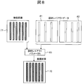
- FIG. 8 is a diagram in which layout data reflecting the parameter A of FIG. 7 and an inspection image including an ideal pattern are superimposed and displayed.
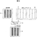
- FIG. 8 is a diagram in which layout data reflecting the parameter A of FIG. 7 and an inspection image including a pattern in which an error occurs are displayed in an overlapping manner.
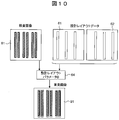
- FIG. 8 is a diagram in which layout data reflecting the parameter B of FIG. 7 and an inspection image including a pattern in which an error occurs are superimposed and displayed.
- FIG. 1 is an overall configuration diagram of a semiconductor defect inspection system according to an embodiment of the present invention.
- the semiconductor defect inspection system 1 in the present embodiment includes a defect inspection device 2, a review device 3, a defect data processing device 4, a design database server 5, and a defect classification device 6.
- the defect inspection device 2, the review device 3, the defect data processing device 4, the design database server 5, and the defect classification device 6 are connected by a network 7 and can mutually transmit and receive data.
- the semiconductor manufacturing process is configured by various processes (not shown) such as impurity implantation, film formation, and etching, and is constructed in a clean room 8 maintained in a clean environment from the necessity of microfabrication.
- a defect inspection apparatus 2 for inspecting a defect on a semiconductor wafer and a review apparatus 3 for observing a defect based on coordinates on the semiconductor wafer are installed.
- the defect inspection device 2 is a dark field defect inspection device, a bright field defect inspection device, an electron beam defect inspection device or the like, and detects a defect generated on the surface of the device to be inspected. Further, the defect inspection apparatus 2 has a function of acquiring an observation image of the detected defect.
- the review device 3 is, for example, a scanning electron microscope (SEM).
- SEM scanning electron microscope
- the defect data processing device 4 receives various data acquired by the defect inspection device 2 and the review device 3 via the network 7 and manages it as defect information data 17.
- the defect information data 17 is stored, for example, in a storage device (not shown) of the defect data processing device 4.
- the defect information data 17 includes a defect data file 18, an image data file 19 and an image information file 10.
- the defect data processing device 4 receives and manages the defect information data 17 obtained by the defect inspection device 2 and the defect information data 17 obtained by the review device 3 via the network 7 respectively.
- the defect data file 18 includes defect identification information for identifying a defect detected by the defect inspection apparatus 2 and the position of the defect with respect to a predetermined reference point (origin) provided on each die (chip). It is a file that stores defect data such as defect position coordinates expressed in a coordinate system on a die, defect size, and category of defect cause.
- the image data file 19 is a file for storing data of a defect image acquired by the defect inspection apparatus 2 or the review apparatus 3 having a review function.
- the image information file 10 is a file that is created in association with each image data file 19 and stores information indicating the acquisition status of each image data file 19. Details of the image information file 10 will be described later.
- the design database server 5 stores design layout data 9 of a semiconductor wafer manufactured in a predetermined semiconductor manufacturing process.
- the design layout data 9 is design data concerning physical arrangement of elements, wirings and the like constituting the semiconductor device, and is data defining the shape (mask pattern) of a mask used in each manufacturing process.
- the design layout data 9 may be defined as a plurality of manufacturing processes (layers) or semiconductor wafer types.
- the design layout data 9 in the current semiconductor manufacturing process has a huge file capacity with the miniaturization of the semiconductor process, and even if the design layout of each manufacturing process alone has a file capacity exceeding several tens of gigabytes, it is difficult to handle It has become As a feature of this embodiment, the design database server 5 divides and stores the design layout data 9.
- the design layout data 9 is divided for each layer (for example, one manufacturing process) of the manufacturing process. Further, the design layout data 9 is divided for each processing step when one layer generates a pattern in a plurality of processing steps (for example, a lithography step) (hereinafter referred to as multi-patterning). Furthermore, the design layout data 9 may be divided for each type of semiconductor wafer.
- the defect classification device 6 acquires defect information data 17 of the semiconductor wafer to be inspected from the defect data processing device 4 and acquires design layout data 9 of the semiconductor wafer from the design database server 5 and overlays the images of both. Display together.
- the defect classification device 6 is configured by an information processing device such as a workstation or a personal computer.
- the defect classification device 6 includes a communication unit (network interface) 120, a processing operation unit 121, a storage unit 122, a layout conversion operation unit 123, a classification determination definition unit 124, a defect determination unit 125, and a user interface 126. Equipped with The configuration of the defect classification device 6 is described as a hardware configuration, but these functions are realized by program code of software, and the program code is executed by the operation unit 121 (CPU) of the defect classification device 6 You may do so.
- the communication unit 120 is an interface for exchanging data with the defect data processing device 4 and the design database server 5. Further, the processing operation unit 121 is configured by a central processing unit (CPU: Central Processing Unit), a microprocessor, or the like, and executes control processing of other units.
- CPU Central Processing Unit
- microprocessor or the like
- the storage unit 122 includes a storage device such as a volatile memory such as a random access memory (RAM), a non-volatile memory such as a flash memory, and a hard disk drive.
- the storage unit 122 stores the defect information data 17 transmitted from the defect data processing device 4 as a defect information data file 29.
- the storage unit 122 also stores the design layout data 9 transmitted from the design database server 5 as a design layout data file 28.
- the storage unit 122 also stores the design layout information file 20 shown in FIG. Details of the design layout information file 20 will be described later.
- the layout conversion operation unit 123 executes graphic conversion processing so that the design layout data 9 sent from the design database server 5 can be read into the system.
- the classification determination definition unit 124 receives defect classification information input by the user interface 126, and defines the classification result in the defect information. Further, the defect determination unit 125 compares the defect image (inspection image) contained in the defect information data file 29 with the reference image to extract a defect position from the defect image.
- the user interface 126 includes an input device such as a keyboard, a mouse and various buttons, and an output device such as a liquid crystal display (LCD) device and a printer.
- an input device such as a keyboard, a mouse and various buttons
- an output device such as a liquid crystal display (LCD) device and a printer.
- the result by the defect classification device 6 is displayed on the output device, and the input from the operator is accepted by the input device.
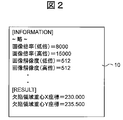
- FIG. 2 is a view showing an example of an image information file according to an embodiment of the present invention.
- the image information file 10 includes the image magnification (low magnification, high magnification) of the defect image included in the image data file 19, the image resolution (low magnification, high magnification), defect area coordinates including defects, barycentric coordinates of defect areas, overlapping.
- it is constituted by information such as the number of frame images constituting the image.
- the image magnification of the defect image is the magnification of the defect image when the defect image is acquired by the defect inspection device 2 or the review device 3.
- the magnification of the defect image is usually the minimum dimension of the pattern defined by the design rule of the semiconductor device, the size of the defect that affects the manufacturing yield of the semiconductor device (defect size), and the defect can be included in the view. It is determined based on a magnification (FOV: Field Of View) or the like.
- the magnification of the defect image is determined at the time of obtaining the defect image, and thus included in the image information file 10 By using the magnification information of each defect, it is possible to match the magnification of the defect image and the layout data.
- FIG. 3 is a view showing an example of a design layout information file according to an embodiment of the present invention.
- layout data included in the design layout data file 28 is divided for each layer of a manufacturing process or for each processing process (for example, a lithography process).
- the design layout information file 20 defines information on combinations of divided layout data, information on offsets of layout data, and the like.
- the design layout information file 20 displays the number of display layouts to be used for display
- the layout configuration for display can be set and configured with a plurality of layout data and the like.
- parameters of pattern expansion amount / reduction amount when displaying each display layout are included, when displaying a defect image and layout data in an overlapping manner, it is possible to perform display with high accuracy with respect to the actual pattern. Become.
- the design layout information file 20 includes at least one of the offset amount of each display layout and the enlargement amount / reduction amount of the display pattern as superposition information when laying out layout data. Further, as the offset amount of the above-mentioned display layout, there are error information between layers (first overlay information) and error information between lithography processes (second overlay information). This makes it possible to correct and display an error between manufacturing steps and an error between lithography steps in multi-patterning.
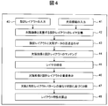
- FIG. 4 is a flowchart showing the process flow of the defect classification device in an embodiment of the invention.
- the layout conversion operation unit 123 acquires layout data included in the design layout data file 28.
- the layout conversion operation unit 123 acquires a defect image included in the defect information data file 29.
- the layout conversion operation unit 123 executes graphic conversion and format conversion processing.
- the processing operation unit 121 executes definition processing of layout data to be displayed overlapping with the defect image.
- the processing operation unit 121 uses the parameters of the design layout information file 20 to define layout data to be displayed overlapping with the defect image.
- layout data may be defined in a plurality of lithography processes as in multi-patterning even in one process.
- the processing operation unit 121 uses the parameters of the design layout information file 20, the processing operation unit 121 combines layout data corresponding to a plurality of lithography processes as one inspection target layer, and associates the layers with each other.
- Each divided layout data has a layer number corresponding to the layer and data type information of the semiconductor wafer to be inspected.
- each layer number and the like are associated with one another, and a plurality of processes are defined as one inspection target. Therefore, the operator should be aware of a plurality of layer numbers and data types on the user interface 126. It becomes possible to treat as one inspection object.
- step 43 the processing operation unit 121 performs origin alignment and magnification alignment of the layout data and the defect image.
- the layout data may have the origin at the center, or the defect may have an image at the bottom left of the die, or both data may have different coordinate systems. Therefore, in step 43, the origin adjustment is performed. In addition, since the magnifications of the layout data and the defect image may be different, magnification adjustment is also performed.
- step 44 the processing operation unit 121 executes matching processing between the layout data and the defect image. Since the coordinate system and the magnification match in step 43, layout data corresponding to the coordinate position can be easily obtained from the coordinate position of the defect. However, data of the coordinate position includes an error at the time of defect detection, and the layout data and the defect image often have some positional deviation. Therefore, here, pattern matching is performed between the layout data and the defect image in a range wider than the visual field of the defect image.
- the processing operation unit 121 collates the layer to be inspected with an arbitrary layer.
- the processing operation unit 121 receives an input from the user interface 126 and collates layout data of the input layer.
- the processing operation unit 121 receives an input from the user interface 126 and collates layout data of the input layer.
- step 46 the processing operation unit 121 superimposes and displays the defect image and the layout data on the display device of the user interface 126.
- the defect image displayed here is an image of a defect position extracted by comparing the defect image and the reference image by the defect determination unit 125.
- step 47 the operator inputs defect classification information at the input device while referring to the superimposed image displayed on the display device of the user interface 126.
- the classification determination definition unit 124 receives the classification information of the defect input by the input device, and defines the classification result for the defect on the defect image.
- step 48 the processing operation unit 121 specifies a defect position from the layout data and the defect image, and executes calculation processing of the defect density, the area ratio, the dimension, and the like of the layer pattern. Finally, the calculation result can be graphed and displayed on the display device as an analysis result to support determination of whether it is a systematic defect or not.
- FIG. 5 is a conceptual view of layer matching processing and overlay display processing.
- a layer that can be a cause of defects is selected from a plurality of layout data divided for each layer (manufacturing process) and collation is performed.
- a portion of layout data corresponding to the defect position of the defect image is acquired.
- the same portion corresponding to the defect position is obtained among the plurality of layers (layer 1 and layer N).
- the defect image, layer 1 and layer N are superimposed and displayed on the display device.
- superposition information for example, offset amount
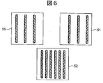
- FIG. 6 is a diagram showing a process of generating a pattern by multi-patterning on a specific layer. In the example of this layer, after the first pattern generation 50 is performed, the second pattern generation 51 is performed. Finally, the target pattern 52 is generated.
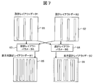
- FIG. 7 shows a diagram in which a plurality of layout data are superimposed using a plurality of parameters.
- the design layout data 9 is divided and stored for each pattern generation process.
- one layer is defined by the pattern 61 of the design layout data 1 and the pattern 62 of the design layout data 2.
- two parameters A (63) and B (64) are set as superposition information.
- the result of overlaying the two patterns 61 and 62 using the parameter A (63) is the overlay result 65.
- the result of overlaying the two patterns 61 and 62 using the parameter B (64) is an overlay result 66.
- the two parameters 63 and 64 may be defined in the design layout information file 20.
- the processing operation unit 121 acquires two parameters 63 and 64 from the design layout information file 20 as superposition information, and superimposes the inspection image and the layout data reflecting the superposition information on the display device. indicate.
- the two parameters may be input by the operator instead of the design layout information file 20.
- the parameter range may be set in advance, and the processing operation unit 121 may automatically calculate a plurality of parameters at predetermined numerical intervals.
- information on a plurality of parameters is stored in advance in the storage unit 122, and after superposition display, the parameters determined to be appropriate by the operator are fed back to the parameter information stored in the storage unit 122 and updated. You may
- FIG. 8 is a diagram in which layout data reflecting the parameter A in FIG. 7 and an inspection image including an ideal pattern are superimposed and displayed.
- the inspection image 71 includes a pattern generated at the design ideal value.
- the parameter A (63) is a parameter for performing superposition with the design ideal values of the two patterns 61 and 62.
- the superposition of the inspection image and the layout data is accurately superimposed.
- the resulting image 72 is obtained.
- FIG. 9 is a diagram in which layout data reflecting the parameter A of FIG. 7 and an inspection image including a pattern in which an error has occurred are superimposed and displayed.
- an error may occur in an actual processing step and a deviation may occur between the two patterns 61 and 62. If the pattern 81 in which an error has occurred is superimposed on the parameter A (63) of the design ideal value of the two patterns 61 and 62, the display does not match and it becomes difficult to perform the analysis and classification processing of the defect.
- FIG. 10 is a diagram in which layout data reflecting the parameter B of FIG. 7 and an inspection image including a pattern in which an error has occurred are superimposed and displayed.
- the parameter B (64) includes the parameter of the offset amount of the two patterns 61 and 62 as superposition information.
- an image 91 is obtained in which the overlay of the inspection image and the layout data is accurately superimposed.
- this offset amount may be obtained from the pattern of the actual inspection image or may be obtained from the shift amount of the layout data display which is a function of the defect classification device 6.
- the spacing between patterns generated in each processing step may not match the design ideal value due to an alignment error or the like of the manufacturing apparatus.
- the defect classification device 6 includes the storage unit 122, the processing operation unit 121, and the user interface 126 including the display device, and the storage unit 122 includes the design layout data file 28 and the defect information data.
- the file 29 is stored, and the processing operation unit 121 superimposes and displays the defect image and the layout data on the display device of the user interface 126.
- the layout image of another layer for example, the layer in the lower layer
- the operator can confirm the presence or absence of the influence of other layers on the defect.
- the layer to be inspected is a Poly-Si layer
- whether the layer under the defect is an N-type or P-type active region (impurity-implanted region) or a non-active region, etc. It is possible to determine whether the defect corresponds to a systematic defect or not based on the information.
- the state (error) of deviation of the active area and the non-active area can be grasped, and the characteristics of the defect can be analyzed in detail.
- defects can be classified based on positional information such as cells, peripheral circuits, and dummy patterns based on layout data.
- the design database server 5 divides and stores the design layout data 9.
- the design layout data 9 is divided for each layer of a manufacturing process, or when one layer generates a pattern in a plurality of processing steps, it is divided for each processing step.
- the storage unit 122 stores the divided design layout data 9 as the design layout data file 28, and the processing operation unit 121 uses the divided layout data to overlap display of the defect image and the layout data. Can be performed. Therefore, the defect analysis and analysis process can be easily and efficiently performed even on the large-scaled design layout data.
- the storage unit 122 stores information such as an offset amount between layers and an offset amount of a pattern in multi-patterning as overlay information on overlay of layout data, and the processing operation unit A display 121 superimposes and displays on the display device the layout data reflecting the superposition information and the inspection image.
- the layer or pattern generated in each process may not match the design ideal value due to an alignment error of the manufacturing apparatus, etc., even in such a case, an offset amount of overlay information is added to the inspection image.
- the information it is possible to match the pattern of the actual inspection image. Therefore, defect analysis and analysis processing can be performed in consideration of manufacturing errors in the actual manufacturing process.
- the offset amount (error information) of the layer or pattern is used as the overlay information in the configuration of the embodiment described above, information of the width of the pattern may also be used. This makes it possible to perform defect analysis and analysis processing in a state in which not only the pattern position of the actual inspection image but also the pattern width match.
- the processing operation unit 121 may acquire layout data of the layer above the layer including the defect (the next process), and further display the layout data of the next process on the inspection image.
- the operator can analyze how much manufacturing error is acceptable in the next step. That is, the operator can analyze the likelihood of the next step in advance.
- the processing operation unit 121 acquires the defect image and the layout data from the design layout data file 28 and the defect information data file 29 of the storage unit 122, but the present invention is not limited to this configuration.
- the processing operation unit 121 may receive layout data directly from the design database server 5 and use it. Further, the processing operation unit 121 may directly receive the defect image from the defect data processing device 4 and use it.
- the configuration of the above-described embodiment can be realized in hardware by designing part or all of them, for example, by an integrated circuit.
- the present invention may be realized by a program code of software that realizes the functions of the embodiment.
- a non-transitory computer readable medium recording the program code is provided to the information processing apparatus (for example, the defect classification apparatus 6), and the information processing apparatus (or CPU or arithmetic unit) Reads the program code stored in the computer readable medium.
- the program code itself read from the computer readable medium implements the functions of the above-described embodiments, and the program code itself and the computer readable medium storing the same constitute the present invention. become.
- Non-transitory computer readable media for supplying such program code include, for example, flexible disk, CD-ROM, DVD-ROM, hard disk, optical disk, magneto-optical disk, CD-R, magnetic tape, non-volatile Memory card, ROM, etc. are used.
- the OS operating system
- the like operating on the defect classification device 6 performs a part or all of the actual processing based on the instruction of the program code, and the functions of the above-described embodiment are realized by the processing.
- the program code is stored in the storage unit of the defect classification device 6 or a storage medium such as CD-RW, CD-R, etc.
- the CPU (or the operation unit) of the defect classification device 6 of the apparatus may read out and execute the program code stored in the storage device or the storage medium.
- control lines and information lines in the drawings indicate what is considered necessary for explanation, and not all control lines and information lines in the product are necessarily shown. All configurations may be connected to each other.
Landscapes
- Engineering & Computer Science (AREA)
- General Physics & Mathematics (AREA)
- Physics & Mathematics (AREA)
- Theoretical Computer Science (AREA)
- Computer Vision & Pattern Recognition (AREA)
- Quality & Reliability (AREA)
- Life Sciences & Earth Sciences (AREA)
- Biochemistry (AREA)
- Immunology (AREA)
- Pathology (AREA)
- General Health & Medical Sciences (AREA)
- Analytical Chemistry (AREA)
- Chemical & Material Sciences (AREA)
- Health & Medical Sciences (AREA)
- Data Mining & Analysis (AREA)
- Artificial Intelligence (AREA)
- Bioinformatics & Cheminformatics (AREA)
- Bioinformatics & Computational Biology (AREA)
- Evolutionary Biology (AREA)
- Evolutionary Computation (AREA)
- General Engineering & Computer Science (AREA)
- Testing Or Measuring Of Semiconductors Or The Like (AREA)
- Signal Processing (AREA)
Priority Applications (2)
| Application Number | Priority Date | Filing Date | Title |
|---|---|---|---|
| US14/395,999 US9881365B2 (en) | 2012-04-23 | 2013-04-11 | Semiconductor defect categorization device and program for semiconductor defect categorization device |
| KR1020147029475A KR101760559B1 (ko) | 2012-04-23 | 2013-04-11 | 반도체 결함 분류 장치 및 반도체 결함 분류 장치용 프로그램을 기록한 비일시적인 컴퓨터 판독 가능 기록 매체 |
Applications Claiming Priority (2)
| Application Number | Priority Date | Filing Date | Title |
|---|---|---|---|
| JP2012097793A JP6080379B2 (ja) | 2012-04-23 | 2012-04-23 | 半導体欠陥分類装置及び半導体欠陥分類装置用のプログラム |
| JP2012-097793 | 2012-04-23 |
Publications (1)
| Publication Number | Publication Date |
|---|---|
| WO2013161577A1 true WO2013161577A1 (ja) | 2013-10-31 |
Family
ID=49482905
Family Applications (1)
| Application Number | Title | Priority Date | Filing Date |
|---|---|---|---|
| PCT/JP2013/060939 Ceased WO2013161577A1 (ja) | 2012-04-23 | 2013-04-11 | 半導体欠陥分類装置及び半導体欠陥分類装置用のプログラム |
Country Status (4)
| Country | Link |
|---|---|
| US (1) | US9881365B2 (https=) |
| JP (1) | JP6080379B2 (https=) |
| KR (1) | KR101760559B1 (https=) |
| WO (1) | WO2013161577A1 (https=) |
Cited By (2)
| Publication number | Priority date | Publication date | Assignee | Title |
|---|---|---|---|---|
| CN110599441A (zh) * | 2018-06-11 | 2019-12-20 | 发那科株式会社 | 接缝检查装置 |
| CN111982927A (zh) * | 2015-05-12 | 2020-11-24 | 东京毅力科创株式会社 | 基板处理系统 |
Families Citing this family (16)
| Publication number | Priority date | Publication date | Assignee | Title |
|---|---|---|---|---|
| JP6771495B2 (ja) * | 2015-08-12 | 2020-10-21 | ケーエルエー コーポレイション | 設計を利用する先行層欠陥箇所の点検 |
| TWI797699B (zh) | 2015-12-22 | 2023-04-01 | 以色列商應用材料以色列公司 | 半導體試樣的基於深度學習之檢查的方法及其系統 |
| US11580375B2 (en) * | 2015-12-31 | 2023-02-14 | Kla-Tencor Corp. | Accelerated training of a machine learning based model for semiconductor applications |
| JP6833366B2 (ja) * | 2016-07-06 | 2021-02-24 | キヤノン株式会社 | 情報処理装置、情報処理装置の制御方法及びプログラム |
| US10650509B2 (en) | 2016-09-08 | 2020-05-12 | Synopsys, Inc. | Video overlay |
| KR102357310B1 (ko) * | 2017-01-18 | 2022-01-28 | 에이에스엠엘 네델란즈 비.브이. | 결함 검토를 위한 정보 추천 |
| KR101753686B1 (ko) * | 2017-02-16 | 2017-07-19 | 강무성 | 회로 해석 및 검증이 가능한 시뮬레이션 시스템 |
| US10402963B2 (en) * | 2017-08-24 | 2019-09-03 | Kla-Tencor Corporation | Defect detection on transparent or translucent wafers |
| WO2019115426A1 (en) * | 2017-12-13 | 2019-06-20 | Asml Netherlands B.V. | Prediction of out of specification physical items |
| CN108318495A (zh) * | 2018-04-11 | 2018-07-24 | 广东理工学院 | 瓷砖检测系统 |
| US12109594B2 (en) * | 2018-06-07 | 2024-10-08 | Wilco Ag | Inspection process |
| JP7053417B2 (ja) * | 2018-09-13 | 2022-04-12 | キオクシア株式会社 | 欠陥検査装置および欠陥検査方法 |
| US10902620B1 (en) * | 2019-04-18 | 2021-01-26 | Applied Materials Israel Ltd. | Registration between an image of an object and a description |
| CN112308816B (zh) * | 2019-07-23 | 2024-02-06 | 纬创资通股份有限公司 | 影像辨识装置、影像辨识方法及其存储介质 |
| CN113804244B (zh) * | 2020-06-17 | 2024-06-25 | 富联精密电子(天津)有限公司 | 缺陷分析方法及装置、电子装置及计算机可读存储介质 |
| CN112036514B (zh) * | 2020-11-04 | 2021-07-13 | 腾讯科技(深圳)有限公司 | 一种图像分类方法、装置、服务器及计算机可读存储介质 |
Citations (2)
| Publication number | Priority date | Publication date | Assignee | Title |
|---|---|---|---|---|
| JP2006215077A (ja) * | 2005-02-01 | 2006-08-17 | Horon:Kk | パターン特定方法およびパターン特定装置 |
| WO2011004534A1 (ja) * | 2009-07-09 | 2011-01-13 | 株式会社 日立ハイテクノロジーズ | 半導体欠陥分類方法,半導体欠陥分類装置,半導体欠陥分類プログラム |
Family Cites Families (4)
| Publication number | Priority date | Publication date | Assignee | Title |
|---|---|---|---|---|
| JP2007102153A (ja) * | 2005-09-08 | 2007-04-19 | Advanced Mask Inspection Technology Kk | 画像補正装置、パターン検査装置、画像補正方法、及びレチクル |
| US20070053583A1 (en) | 2005-09-08 | 2007-03-08 | Advanced Mask Inspection Technology Inc. | Image correcting apparatus, pattern inspection apparatus, and image correcting method, and reticle |
| JP5068591B2 (ja) | 2007-06-29 | 2012-11-07 | 株式会社日立ハイテクノロジーズ | 半導体欠陥分類方法、半導体欠陥分類装置、半導体欠陥分類装置のプログラム、半導体欠陥検査方法、および、半導体欠陥検査システム |
| US8980651B2 (en) * | 2011-09-30 | 2015-03-17 | Tokyo Electron Limited | Overlay measurement for a double patterning |
-
2012
- 2012-04-23 JP JP2012097793A patent/JP6080379B2/ja active Active
-
2013
- 2013-04-11 US US14/395,999 patent/US9881365B2/en active Active
- 2013-04-11 WO PCT/JP2013/060939 patent/WO2013161577A1/ja not_active Ceased
- 2013-04-11 KR KR1020147029475A patent/KR101760559B1/ko active Active
Patent Citations (2)
| Publication number | Priority date | Publication date | Assignee | Title |
|---|---|---|---|---|
| JP2006215077A (ja) * | 2005-02-01 | 2006-08-17 | Horon:Kk | パターン特定方法およびパターン特定装置 |
| WO2011004534A1 (ja) * | 2009-07-09 | 2011-01-13 | 株式会社 日立ハイテクノロジーズ | 半導体欠陥分類方法,半導体欠陥分類装置,半導体欠陥分類プログラム |
Cited By (4)
| Publication number | Priority date | Publication date | Assignee | Title |
|---|---|---|---|---|
| CN111982927A (zh) * | 2015-05-12 | 2020-11-24 | 东京毅力科创株式会社 | 基板处理系统 |
| CN111982927B (zh) * | 2015-05-12 | 2023-12-15 | 东京毅力科创株式会社 | 基板处理系统 |
| CN110599441A (zh) * | 2018-06-11 | 2019-12-20 | 发那科株式会社 | 接缝检查装置 |
| CN110599441B (zh) * | 2018-06-11 | 2023-11-07 | 发那科株式会社 | 接缝检查装置 |
Also Published As
| Publication number | Publication date |
|---|---|
| JP2013225618A (ja) | 2013-10-31 |
| US20150213596A1 (en) | 2015-07-30 |
| KR20140147850A (ko) | 2014-12-30 |
| JP6080379B2 (ja) | 2017-02-15 |
| KR101760559B1 (ko) | 2017-07-21 |
| US9881365B2 (en) | 2018-01-30 |
Similar Documents
| Publication | Publication Date | Title |
|---|---|---|
| JP6080379B2 (ja) | 半導体欠陥分類装置及び半導体欠陥分類装置用のプログラム | |
| US11761904B2 (en) | Smart defect calibration system in semiconductor wafer manufacturing | |
| JP5479782B2 (ja) | 欠陥画像処理装置、欠陥画像処理方法、半導体欠陥分類装置および半導体欠陥分類方法 | |
| JP5021503B2 (ja) | パターン欠陥解析装置、パターン欠陥解析方法およびパターン欠陥解析プログラム | |
| JP5357725B2 (ja) | 欠陥検査方法及び欠陥検査装置 | |
| US20100138801A1 (en) | System and Method for Detecting a Defect | |
| US8675949B2 (en) | Reviewed defect selection processing method, defect review method, reviewed defect selection processing tool, and defect review tool | |
| JP2009123851A (ja) | 欠陥観察分類方法及びその装置 | |
| WO2011004534A1 (ja) | 半導体欠陥分類方法,半導体欠陥分類装置,半導体欠陥分類プログラム | |
| JP2011222622A (ja) | 検査方法およびその装置 | |
| JP2008268560A (ja) | ホットスポット絞り込み装置、ホットスポット絞り込み方法、ホットスポット絞り込みプログラム、ホットスポット検査装置、および、ホットスポット検査方法 | |
| JP4641924B2 (ja) | 半導体検査装置及び半導体検査方法 | |
| JP5323457B2 (ja) | 観察条件決定支援装置および観察条件決定支援方法 | |
| JP2013236031A (ja) | 欠陥分類装置、欠陥分類方法 | |
| JP5396407B2 (ja) | パターン観察装置,レシピ作成装置,レシピ作成方法 | |
| JP5469704B2 (ja) | 欠陥解析装置、欠陥解析方法および欠陥解析プログラム | |
| JP5039594B2 (ja) | レビュー装置,検査領域設定支援システム、および、欠陥の画像得方法 |
Legal Events
| Date | Code | Title | Description |
|---|---|---|---|
| 121 | Ep: the epo has been informed by wipo that ep was designated in this application |
Ref document number: 13781553 Country of ref document: EP Kind code of ref document: A1 |
|
| ENP | Entry into the national phase |
Ref document number: 20147029475 Country of ref document: KR Kind code of ref document: A |
|
| WWE | Wipo information: entry into national phase |
Ref document number: 14395999 Country of ref document: US |
|
| NENP | Non-entry into the national phase |
Ref country code: DE |
|
| 122 | Ep: pct application non-entry in european phase |
Ref document number: 13781553 Country of ref document: EP Kind code of ref document: A1 |