WO2013146239A1 - 感光性導電ペーストおよび導電性配線付き基板の製造方法 - Google Patents
感光性導電ペーストおよび導電性配線付き基板の製造方法 Download PDFInfo
- Publication number
- WO2013146239A1 WO2013146239A1 PCT/JP2013/056918 JP2013056918W WO2013146239A1 WO 2013146239 A1 WO2013146239 A1 WO 2013146239A1 JP 2013056918 W JP2013056918 W JP 2013056918W WO 2013146239 A1 WO2013146239 A1 WO 2013146239A1
- Authority
- WO
- WIPO (PCT)
- Prior art keywords
- photosensitive
- conductive paste
- substrate
- electrode
- conductive
- Prior art date
- Legal status (The legal status is an assumption and is not a legal conclusion. Google has not performed a legal analysis and makes no representation as to the accuracy of the status listed.)
- Ceased
Links
Classifications
-
- G—PHYSICS
- G03—PHOTOGRAPHY; CINEMATOGRAPHY; ANALOGOUS TECHNIQUES USING WAVES OTHER THAN OPTICAL WAVES; ELECTROGRAPHY; HOLOGRAPHY
- G03F—PHOTOMECHANICAL PRODUCTION OF TEXTURED OR PATTERNED SURFACES, e.g. FOR PRINTING, FOR PROCESSING OF SEMICONDUCTOR DEVICES; MATERIALS THEREFOR; ORIGINALS THEREFOR; APPARATUS SPECIALLY ADAPTED THEREFOR
- G03F7/00—Photomechanical, e.g. photolithographic, production of textured or patterned surfaces, e.g. printing surfaces; Materials therefor, e.g. comprising photoresists; Apparatus specially adapted therefor
- G03F7/004—Photosensitive materials
- G03F7/0047—Photosensitive materials characterised by additives for obtaining a metallic or ceramic pattern, e.g. by firing
-
- G—PHYSICS
- G03—PHOTOGRAPHY; CINEMATOGRAPHY; ANALOGOUS TECHNIQUES USING WAVES OTHER THAN OPTICAL WAVES; ELECTROGRAPHY; HOLOGRAPHY
- G03F—PHOTOMECHANICAL PRODUCTION OF TEXTURED OR PATTERNED SURFACES, e.g. FOR PRINTING, FOR PROCESSING OF SEMICONDUCTOR DEVICES; MATERIALS THEREFOR; ORIGINALS THEREFOR; APPARATUS SPECIALLY ADAPTED THEREFOR
- G03F7/00—Photomechanical, e.g. photolithographic, production of textured or patterned surfaces, e.g. printing surfaces; Materials therefor, e.g. comprising photoresists; Apparatus specially adapted therefor
- G03F7/004—Photosensitive materials
- G03F7/027—Non-macromolecular photopolymerisable compounds having carbon-to-carbon double bonds, e.g. ethylenic compounds
-
- H—ELECTRICITY
- H01—ELECTRIC ELEMENTS
- H01B—CABLES; CONDUCTORS; INSULATORS; SELECTION OF MATERIALS FOR THEIR CONDUCTIVE, INSULATING OR DIELECTRIC PROPERTIES
- H01B1/00—Conductors or conductive bodies characterised by the conductive materials; Selection of materials as conductors
- H01B1/20—Conductive material dispersed in non-conductive organic material
- H01B1/22—Conductive material dispersed in non-conductive organic material the conductive material comprising metals or alloys
-
- H—ELECTRICITY
- H05—ELECTRIC TECHNIQUES NOT OTHERWISE PROVIDED FOR
- H05K—PRINTED CIRCUITS; CASINGS OR CONSTRUCTIONAL DETAILS OF ELECTRIC APPARATUS; MANUFACTURE OF ASSEMBLAGES OF ELECTRICAL COMPONENTS
- H05K1/00—Printed circuits
- H05K1/02—Details
- H05K1/09—Use of materials for the conductive, e.g. metallic pattern
- H05K1/092—Dispersed materials, e.g. conductive pastes or inks
-
- H—ELECTRICITY
- H05—ELECTRIC TECHNIQUES NOT OTHERWISE PROVIDED FOR
- H05K—PRINTED CIRCUITS; CASINGS OR CONSTRUCTIONAL DETAILS OF ELECTRIC APPARATUS; MANUFACTURE OF ASSEMBLAGES OF ELECTRICAL COMPONENTS
- H05K2203/00—Indexing scheme relating to apparatus or processes for manufacturing printed circuits covered by H05K3/00
- H05K2203/05—Patterning and lithography; Masks; Details of resist
- H05K2203/0502—Patterning and lithography
- H05K2203/0514—Photodevelopable thick film, e.g. conductive or insulating paste
-
- H—ELECTRICITY
- H05—ELECTRIC TECHNIQUES NOT OTHERWISE PROVIDED FOR
- H05K—PRINTED CIRCUITS; CASINGS OR CONSTRUCTIONAL DETAILS OF ELECTRIC APPARATUS; MANUFACTURE OF ASSEMBLAGES OF ELECTRICAL COMPONENTS
- H05K3/00—Apparatus or processes for manufacturing printed circuits
- H05K3/10—Apparatus or processes for manufacturing printed circuits in which conductive material is applied to the insulating support in such a manner as to form the desired conductive pattern
Definitions
- the present invention relates to a method for producing a photosensitive conductive paste and a substrate with conductive wiring.
- conductive paste for forming patterned conductive wiring by coating, drawing, and printing on substrates such as glass, ceramics, and composite materials is relatively inexpensive and excellent in microfabrication. It is used in fields such as solar cells. While maintaining and improving performances such as conductivity and fine workability, reduction of environmental burden and cost reduction have attracted attention in recent years.
- General conductive paste used in these applications includes an inorganic powder containing conductive powder and glass frit, and an organic binder. After applying such a conductive paste in a specific pattern on a substrate or forming a conductive paste coating film having a desired pattern by patterning after coating, the organic binder is baked in air at 500 ° C. or higher.
- the conductive wiring made of a conductive material and glass is formed by removing and softening the glass frit.
- a plasma display panel can display at a higher speed than a liquid crystal panel and can be easily increased in size, and thus has penetrated into fields such as OA equipment and public information display devices. It is also used in the field of high-definition television.
- a slight gap formed between two glass substrates of a front plate and a back plate is used as a discharge space, and plasma discharge is generated between the anode electrode and the cathode electrode, and is enclosed in the discharge space.
- the display is performed by emitting ultraviolet light generated from the gas to a phosphor provided in the discharge space.
- the electrodes are provided in stripes on the front plate and the back plate, and a plurality of electrodes are provided in parallel.
- the electrodes on the front plate and the electrodes on the back plate face each other with a slight gap and are orthogonal to each other. To be formed.
- a plurality of electrode pairs formed of display electrodes adjacent to each other in parallel are provided on the front plate and orthogonal to each electrode pair.
- a plurality of address electrodes provided on the back plate.
- a barrier rib for preventing crosstalk of light and securing a discharge space is formed in the space between the electrodes on the back plate.
- a phosphor is formed in the discharge space.
- the address electrodes formed on the back plate need to have a uniform thickness and line width over a wide range. Furthermore, with the higher definition of PDPs, the fine pitch of address electrodes is progressing.
- the line shape is bent and swelled even after the baking process because the baking process is performed at a temperature of 500 ° C. or higher in the air as described above.
- a photosensitive paste using a noble metal such as silver or gold as the conductive powder (for example, Patent Document 1).
- the electrode paste used in Patent Document 1 has a problem of high cost because it contains a noble metal.
- the photosensitive conductive pastes of Patent Documents 1 and 2 have various firing environments such as an oxygen-deficient condition in which the amount of air supply and exhaust in the firing furnace is insufficient, and a condition of simultaneously firing the electrode, dielectric, and partition walls described in Patent Document 3. Assuming that, the organic binder component remaining in the firing process hinders uniform progress of sintering at the start of sintering, and there is a problem that sintering proceeds only between adjacent conductive powders. Since the conductive powder apparently grows large and breaks without forming a dense fired film, it is not sufficient for various firing environments.
- a photosensitive conductive paste using titanium oxide is provided with a dense fired film that does not cause disconnection according to various firing environments, an inexpensive conductive wiring characterized by an appropriate shape and a desired resistance value. It aims at providing the photosensitive electrically conductive paste which can be formed.
- the photosensitive conductive paste of the present invention has the following configuration. That is, a photosensitive conductive paste containing conductive powder, an inorganic component containing glass frit and titanium oxide particles, and a photosensitive organic component, wherein the content of the titanium oxide particles is 100 parts by weight of the conductive powder.
- the photosensitive conductive paste is characterized by having a volume average particle size of 0.001 to 1.0 ⁇ m.
- the photosensitive conductive paste of the present invention it is possible to form a dense fired film that does not cause disconnection, an inexpensive conductive wiring characterized by an appropriate shape and resistance value according to various firing environments. It aims at providing a conductive paste.
- the titanium oxide particles used in the present invention have the effect of delaying the timing of starting silver sintering and promoting evaporation of the remaining organic binder component. Therefore, it is necessary to mix titanium oxide particles appropriately.
- the content of titanium oxide particles is preferably in the range of 0.1 to 5.0 parts by weight with respect to 100 parts by weight of the conductive powder. This is because if the organic binder component in the electrode is baked under conditions that tend to remain, if it is less than 0.1 part by weight, sintering proceeds nonuniformly and a dense fired film cannot be formed. Because. On the other hand, if the amount exceeds 5.0 parts by weight, sintering of the conductive powder is hindered, resulting in problems such as insufficient adhesion strength and high resistance.
- the volume average particle diameter of the titanium oxide particles is preferably 0.001 to 1.0 ⁇ m. If it is less than 0.001 ⁇ m, the titanium oxide particles are likely to aggregate, making it difficult to disperse in the paste, causing bias when forming the conductive wiring, causing poor conduction, and effects on silver sintering and organic binder evaporation. Cannot be fully demonstrated. If the thickness exceeds 1.0 ⁇ m, silver sintering is hindered, resulting in problems such as insufficient adhesion strength and high resistance.
- the titanium oxide particles used in the present invention are one type of filler that is an inorganic powder other than the conductive powder, and have no softening point, melting point, decomposition point, etc. at 600 ° C. or lower.
- the conductive powder used in the present invention may be any conductive powder, and preferably contains at least one selected from the group consisting of Ag, Au, Pd, Ni, Cu, Al and Pt, and has low resistance.
- the conductive powder is preferable. More preferably, Ag or silver. These can be used independently, in an alloy state, or in a mixed powder state.
- the volume average particle diameter of the conductive powder is preferably 0.1 to 2.5 ⁇ m, and the content is preferably 35 mass% to 54 mass%. When the amount is less than 35% by mass, the contact probability between the conductive powders decreases, and a disconnection failure or a conduction failure occurs.
- the specific surface area of the conductive powder is preferably 0.3 to 2.5 m 2 / g in view of the accuracy of the conductive wiring. More preferably, the specific surface area is 0.35 to 2.0 m 2 / g.
- the tap density of the conductive powder is preferably 3 to 6 g / cm 2 . More preferably, it is in the range of 3.5 to 5 g / cm 2 .
- the shape of the conductive powder is preferably spherical, and more preferably a sharp particle size distribution and few aggregates. In this case, the spherical shape means that the sphericity is 90% by number or more. The sphericity is obtained by photographing powder with an optical microscope at a magnification of 300 times, counting the particles that can be counted, and representing the ratio of the spheres.
- a value obtained by multiplying A and B by A ⁇ B Is preferably in the range of 0.1-12. This is based on the particle size of the conductive particles if the value A ⁇ B obtained by multiplying A and B is less than 0.1 when fired under conditions such that the organic binder component in the electrode tends to remain. This is because the amount of titanium oxide particles added is insufficient and a uniform fired film may not be formed.
- the glass frit in the present invention is preferably used in the range of 3 to 20 parts by weight with respect to 100 parts by weight of the conductive powder in order to firmly bake the conductive powder on the substrate. More preferably, it is in the range of 5 to 20 parts by weight with respect to 100 parts by weight of the conductive powder. Further, the glass frit has an effect of sintering aid for sintering conductive powder and an effect of lowering conductor resistance. When the content of the glass frit is less than 3 parts by weight with respect to 100 parts by weight of the conductive powder, the adhesion strength between the substrate and the conductive wiring is reduced, and there is a case where the conductive wiring is peeled off from the substrate.
- the sinterability between the conductive powders is deteriorated, there may be a problem that the resistance of the obtained wiring is increased.
- the content of the glass frit is more than 20 parts by weight with respect to 100 parts by weight of the conductive powder, the photosensitive organic component is not sufficiently evaporated, which causes swelling of the conductive wiring after firing. There is a case.
- the glass transition temperature (Tg) and softening point (Ts) of the glass frit used for the photosensitive conductive paste of the present invention are preferably in the range of 400 to 600 ° C. and 450 to 700 ° C., respectively.
- one or more kinds of glass frit having different transition points and softening points can be used.
- the powder particle size of the glass frit is preferably such that the volume average particle size is 0.1 to 1.4 ⁇ m, the 90% particle size is 1 to 2 ⁇ m, and the top size is 4.5 ⁇ m or less.
- the volume average particle size and the 90% particle size in the volume-based particle size distribution curve are less than 0.5 ⁇ m and 1 ⁇ m, respectively, the glass frit particle size becomes too small and ultraviolet rays are scattered to the unexposed area, and the edge of the conductor film -Photocuring of the end portion may occur and development may be impossible, and there is a tendency that the pattern of the conductive film is cut and the resolution is lowered.
- the coarse glass frit and the conductive powder differ in thermal expansion coefficient.
- the adhesive strength of the conductor film is lowered, so that the film may be peeled off, and the coarse glass frit remains in the conductor film, and the adhesive strength tends to be lowered.
- Bi 2 O 3 is preferably blended in the range of 30 to 70% by mass.
- the softening point of the glass frit becomes low and the glass frit melts before the binder in the photosensitive conductive paste evaporates. For this reason, the debinding property of the paste is deteriorated, the sinterability of the conductor film is lowered, and the adhesive strength with the substrate tends to be lowered.
- the glass frit is 30 to 70% by mass of Bi 2 O 3 in terms of oxide. SiO 2 5-30% by mass B 2 O 3 6-20% by mass ZrO 2 3-10% by mass Al 2 O 3 1-5% by mass It is preferable that it is an alkali-free glass frit which contains 80 mass% or more of the composition range and contains substantially no Na 2 O, K 2 O or Li 2 O. Within this range, a glass frit can be obtained in which the conductor film can be firmly fired on the substrate at a preferred firing temperature of 550 to 600 ° C. when a glass substrate is used.
- the photosensitive polymer can be obtained by polymerization or copolymerization of components selected from compounds having a carbon-carbon double bond.
- an unsaturated acid such as an unsaturated carboxylic acid
- an unsaturated carboxylic acid include acrylic acid, methacrylic acid, itaconic acid, crotonic acid, maleic acid, fumaric acid, vinyl acetic acid, and acid anhydrides thereof.
- the acid value of the polymer or oligomer having an acidic group such as a carboxyl group in the side chain thus obtained is preferably 50 to 180 mgKOH / g, more preferably 70 to 140 mgKOH / g.
- the photosensitive conductive paste of the present invention contains a photosensitive organic component.
- the photosensitive organic component preferably contains a photosensitive polymer and / or a photosensitive monomer.
- photosensitive polymers examples include methyl (meth) acrylate, ethyl (meth) acrylate, normal butyl (meth) acrylate, isobutyl (meth) acrylate, isopropyl (meth) acrylate, 2-ethylmethyl (meth) acrylate, 2-hydroxyl
- Preferred photoreactive groups are those having an ethylenically unsaturated group.
- Examples of the ethylenically unsaturated group include a vinyl group, an allyl group, an acrylic group, and a methacryl group.
- the content of the photosensitive polymer in the photosensitive conductive paste of the present invention is preferably 1 to 30% by mass, more preferably 2 to 30% by mass.
- the photosensitive monomer examples include methyl acrylate, ethyl acrylate, n-propyl acrylate, isopropyl acrylate, n-butyl acrylate, sec-butyl acrylate, sec-butyl acrylate, isobutyl acrylate, tert-butyl acrylate, n-pentyl.
- the photosensitive organic component is contained in an amount of 5 to 40 parts by weight with respect to 100 parts by weight of the conductive powder. Further, it is preferably contained in an amount of 10 to 35 parts by weight.
- the photosensitive conductive paste of the present invention further includes cellulose resins such as ethyl cellulose, methyl cellulose, nitrocellulose, cellulose acetate, cellulose propionate, and cellulose butyrate, poly- ⁇ -methyl sulfone, and polyvinyl.
- cellulose resins such as ethyl cellulose, methyl cellulose, nitrocellulose, cellulose acetate, cellulose propionate, and cellulose butyrate, poly- ⁇ -methyl sulfone, and polyvinyl.
- Non-photosensitive polymers such as alcohol or polybutene can be contained.
- the photosensitive conductive paste of the present invention preferably uses a photopolymerization initiator, a sensitizer, a polymerization inhibitor, and an organic solvent as necessary.
- photopolymerization initiator examples include benzophenone, methyl o-benzoylbenzoate, 4,4′-bis (dimethylamino) benzophenone, 4,4′-bis (diethylamino) benzophenone, 4,4′-dichloro.
- the sensitizer is preferably added in order to improve sensitivity.
- Specific examples of the sensitizer include 2,3-bis (4-diethylaminobenzal) cyclopentanone, 2,6-bis (4-dimethylaminobenzal) cyclohexanone, and 2,6-bis (4-dimethylamino).
- the addition amount is 0.1 to 10% by mass, more preferably 0.2 to 5% by mass with respect to the photosensitive organic component. If the amount of the sensitizer is too small, the effect of improving the photosensitivity is not exhibited, and if the amount of the sensitizer is too large, the residual ratio of the exposed portion may be too small.
- a polymerization inhibitor to the photosensitive conductive paste in order to improve the thermal stability during storage.
- the polymerization inhibitor include hydroquinone, hydroquinone monomethyl ether, N-nitrosodiphenylamine, phenothiazine, pt-butylcatechol, N-phenylnaphthylamine, 2,6-di-tert-butyl-p-methylphenol. , Chloranil, pyrogallol and the like.
- the addition amount is preferably 0.1 to 5% by mass, more preferably 0.2 to 3% by mass in the photosensitive conductive paste. If the amount of the polymerization inhibitor is too small, the effect of improving the thermal stability during storage is not exhibited, and if the amount of the polymerization inhibitor is too large, the residual ratio of the exposed portion may be too small.
- an organic solvent may be added to the photosensitive conductive paste of the present invention.
- the organic solvent used at this time include methyl cellosolve, ethyl cellosolve, butyl cellosolve, methyl ethyl ketone, dioxane, acetone, cyclohexanone, cyclopentanone, isobutyl alcohol, isopropyl alcohol, tetrahydrofuran, dimethyl sulfoxide, and ⁇ -butyrolactone. It is done.
- These organic solvents are used alone or in combination of two or more.
- the composition of the photosensitive conductive paste of the present invention is preferably selected within the following range.
- Conductive powder 35-54% by mass with respect to the entire conductive paste
- Glass frit within the range of 3 to 20 parts by weight, preferably within the range of 5 to 20 parts by weight with respect to 100 parts by weight of the conductive powder.
- Titanium oxide particles 0.1 to 5. with respect to 100 parts by weight of the conductive powder.
- Photosensitive organic component 5 to 40% by mass, preferably 10 to 35% by mass, based on 100 parts by weight of conductive powder
- the ultraviolet rays are well transmitted at the time of exposure, the function of photocuring is sufficiently exerted, the film strength of the exposed area at the time of development is increased, and the conductive wiring having fine resolution Can be formed.
- a dense fired film having high adhesion strength between the substrate and the conductive wiring, low resistance, and no disconnection can be formed.
- a method for producing the photosensitive conductive paste of the present invention will be described.
- the slurry adjusted to have a predetermined composition is homogeneously mixed with a stirrer such as a homogenizer and then uniformly dispersed with a three roller or kneader to produce a paste.
- the viscosity of the photosensitive conductive paste is appropriately adjusted depending on the ratio of addition of conductive powder, glass frit, inorganic filler, organic solvent, organic component composition / type, plasticizer, thixotropic agent, suspending agent, organic leveling agent, etc.
- the range is preferably within the range of 10 to 150 Pa ⁇ s at 3 rpm.
- a bar coater, a roller coater or an applicator it is preferably within a range of 30 to 100 Pa ⁇ s.
- the method for producing a substrate with conductive wiring according to the present invention is characterized in that the above-mentioned photosensitive conductive paste is applied on a substrate, patterned by photolithography, and then baked to form conductive wiring.
- the photosensitive conductive paste of the present invention can be finely patterned, has high adhesion strength between the substrate and the conductive wiring, and in various firing environments, the resistance value of the conductive wiring after firing is A low and dense fired film can be formed.
- the photosensitive conductive paste of the present invention is usually applied on a glass substrate by a screen printing method.
- the printing thickness can be arbitrarily controlled by adjusting the screen material (polyester or stainless steel), 250 to 380 mesh screen, and adjusting the screen opening, screen tension, paste viscosity, etc.
- the thickness is in the range of 0.1 to 25 ⁇ m, and a more preferable thickness range is 0.1 to 15 ⁇ m.
- the thickness is less than 0.1 ⁇ m, it is difficult to obtain a uniform thickness by the printing method.
- the thickness exceeds 25 ⁇ m, the accuracy of the electrode pattern decreases, and the cross-sectional shape becomes an inverted trapezoid. For example, when trying to form a high-definition pattern having a minimum line width / minimum width interval of 30 ⁇ m / 30 ⁇ m or less, Edge cutting is worse.
- a glass substrate using a high strain point glass such as soda glass, “PD-200” manufactured by Asahi Glass Co., Ltd., or “PP-8” manufactured by Nippon Electrochemical Co., Ltd. is usually used.
- the film in which the photosensitive conductive paste is applied on the substrate is heated at 130 ° C. for 10 minutes to dry to evaporate the solvents, and then pattern exposure is performed to photocure the photosensitive conductive paste.
- development is carried out using the difference in solubility between the exposed portion and the unexposed portion in the developer to form an electrode pattern.
- an immersion method, a spray method, a brush method, or the like is used.
- a solution capable of dissolving the organic components in the photosensitive conductive paste, particularly the polymer may be used.
- the substrate is baked while being held at 590 ° C. for 10 minutes in an air atmosphere, and a striped electrode having a thickness of 1.5 ⁇ m is formed after baking.
- Example and comparative example of this invention The material used for the Example and comparative example of this invention is shown below.
- Conductive powder manufactured by a wet reduction method, silver powder having a specific surface area of 0.41 m 2 / g and a tap density of 5.0 g / cm 3 was used.
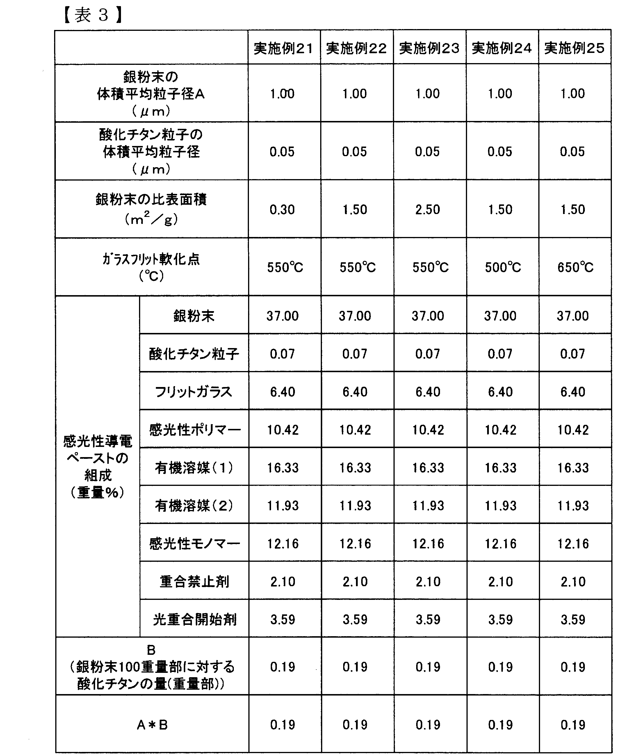
- Tables 1 to 3 show the volume average particle diameters of the silver powder used in each example and comparative example.
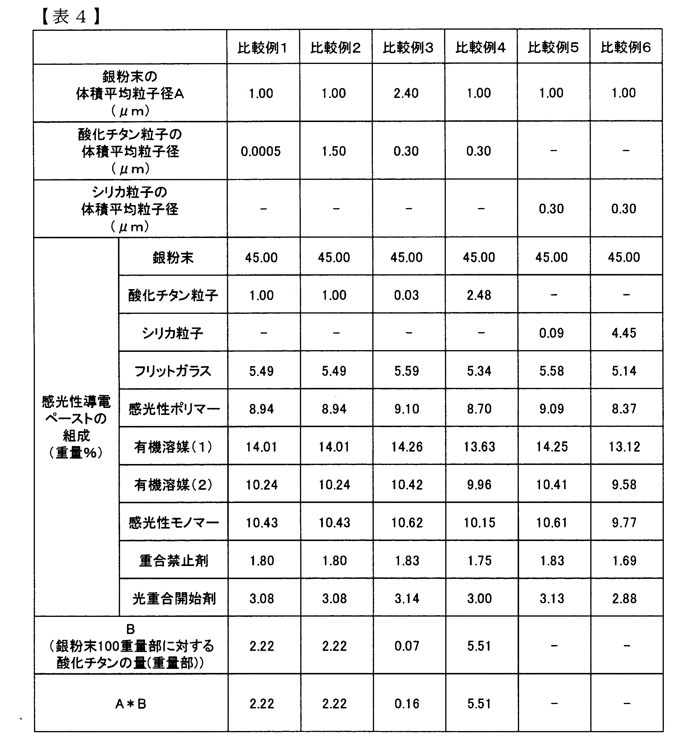
- Frit glass Bismuth oxide (48.1% by mass) Silicon dioxide (27.5% by mass), Boron oxide (14.2% by mass), Zinc oxide (2.6% by mass), Aluminum oxide (2.8% by mass) ), Zirconium oxide (4.8% by mass), a volume average particle size of 0.9 ⁇ m, a glass transition point (Tg) of 465 ° C., and a thermal softening point (Ts) of 510 ° C. were used. . Titanium oxide particles: Titanium oxide particles having volume average particle diameters shown in Tables 1 to 4 were used. Silica particles: In Comparative Examples 5 and 6, silica particles having the volume average particle diameter shown in Table 4 were used.
- Photopolymer A polymer obtained by copolymerizing acrylic acid, methyl methacrylate and styrene in a weight ratio of 40/30/30, and adding 0.4 mol of glycidyl methacrylate to 1 mol of acrylic acid (weight average molecular weight 32, 000, acid value 110)
- Organic solvent 1 Diethylene glycol monobutyl ether acetate
- Organic solvent 2 2,2,4-trimethyl-1,3-pentanediol monoisobutyrate
- Photosensitive monomer Trimethylolpropane triacrylate polymerization inhibitor: Hydroquinone monomethyl ether photopolymerization initiator : IRGACURE651
- Tables 1 to 4 To obtain 31 types of pastes.
- volume average particle diameter of silver powder, titanium oxide particles, and silica particles was measured using a dynamic light scattering particle size distribution meter manufactured by HORIBA.
- a photosensitive conductive paste was applied to the entire surface of a glass substrate (PD-200; manufactured by Asahi Glass Co., Ltd.) having a size of 340 ⁇ 260 ⁇ 2.8 mm with a screen printer.
- the solvent was dried at 130 ° C. for 10 minutes, pattern exposure was performed with an ultrahigh pressure mercury lamp using a photomask, and a pattern was obtained by shower development with an aqueous 0.1% 2-aminoethanol solution at 35 ° C.
- the substrate was held at 590 ° C. for 10 minutes in an air atmosphere and baked to form a striped electrode and evaluated.
- the electrode line width is 40 ⁇ m
- the line length is 80 cm
- the electrode conduction failure is evaluated using an inspection device (manufactured by Nidec Lead).
- 20,000 electrodes were inspected, and a case where the defect rate was less than 2% was indicated by “ ⁇ ”, and a case where the defect rate was 2% or more was indicated by “X”.
- the evaluation results are shown in Table 5.
- the substrate was held in an air atmosphere at 590 ° C. for 10 minutes and fired to form a striped electrode for evaluation.
- the electrode line width was 65 ⁇ m and the line length was 60 cm, and the line resistance was evaluated using a tester.
- the case of 1000 ⁇ or less was indicated by “ ⁇ ”
- the case of 1000 to 2000 ⁇ was indicated by “ ⁇ ”
- the case where measurement was not possible was indicated by “X”.
- the evaluation results are shown in Table 5.
- the substrate was held in an air atmosphere at 590 ° C. for 10 minutes and fired to form a striped electrode for evaluation.
- the pattern edge was evaluated using a digital force gauge DFG-5KR (manufactured by Nidec Symposium). Solder the connection jig to the pattern for adhesion strength measurement, pull it in the right angle direction, measure the strength 20 times when the measurement part of 2mm square is removed from the substrate, and find the average value, when 1.5kgf or more Is “ ⁇ ”, and the case where it is smaller than 1.5 kgf is “x”.
- the evaluation results are shown in Table 5.
- Example 1 which are within the scope of the present application, good results were obtained in all evaluations.
- Comparative Example 1 in which the volume average particle diameter of the titanium oxide particles was too small, and comparison in which the addition amount of the titanium oxide particles was too small
- Example 3 and Comparative Examples 5 and 6 using inorganic fillers other than titanium oxide particles when fired under conditions in which the organic binder component in the electrode was likely to remain, lack of compactness and poor conduction occurred.
Landscapes
- Physics & Mathematics (AREA)
- Chemical & Material Sciences (AREA)
- Dispersion Chemistry (AREA)
- General Physics & Mathematics (AREA)
- Spectroscopy & Molecular Physics (AREA)
- Engineering & Computer Science (AREA)
- Ceramic Engineering (AREA)
- Microelectronics & Electronic Packaging (AREA)
- Conductive Materials (AREA)
- Devices For Indicating Variable Information By Combining Individual Elements (AREA)
- Gas-Filled Discharge Tubes (AREA)
- Parts Printed On Printed Circuit Boards (AREA)
- Manufacturing Of Printed Circuit Boards (AREA)
- Manufacturing Of Electric Cables (AREA)
Abstract
Description
Bi2O3 30~70質量%
SiO2 5~30質量%
B2O3 6~20質量%
ZrO2 3~10質量%
Al2O3 1~5質量%
の組成範囲からなるものを80質量%以上含有し、かつNa2O,K2O,Li2Oを実質的に含有しないアルカリフリーのガラスフリットであることが好ましい。この範囲であると、ガラス基板を用いる場合の好ましい焼成温度である550~600℃で導体膜を基板上に強固に焼成できるガラスフリットが得られる。
本発明の感光性導電ペーストにおける感光性ポリマーの含有量は、1~30質量%、さらには、2~30質量%であることが好ましい。
導電性粉末:導電ペースト全体に対して35~54質量%
ガラスフリット:導電性粉末100重量部に対して3~20重量部の範囲内、好ましくは5~20重量部の範囲内
酸化チタン粒子:導電性粉末100重量部に対して0.1~5.0質量%
感光性有機成分:導電性粉末100重量部に対して5~40質量%が好ましく、さらに好ましくは10~35質量%
各成分の量が上述の範囲内であると露光時において紫外線がよく透過し、光硬化の機能が十分発揮され、現像時における露光部の膜強度が高くなり、微細な解像度を有する導電性配線が形成できる。また基板と導電性配線の密着強度が高く、低抵抗、かつ断線が発生しない緻密な焼成膜を形成することができる。
導電性粉末:湿式還元法により製造されたもので比表面積0.41m2/g、タップ密度5.0g/cm3の銀粉末を用いた。各実施例、比較例で用いた銀粉末の体積平均粒子径を表1~3に示す。
フリットガラス:酸化ビスマス(48.1質量%)二酸化ケイ素(27.5質量%)、酸化ホウ素(14.2質量%),酸化亜鉛(2.6質量%)、酸化アルミニウム(2.8質量%)、酸化ジルコニウム(4.8質量%)の成分比を持ち、体積平均粒子径が0.9μm、ガラス転移点(Tg)が465℃、熱軟化点(Ts)が510℃のものを用いた。
酸化チタン粒子:表1~4に示す体積平均粒子径を有する酸化チタン粒子を用いた。
シリカ粒子:比較例5および6では表4に示す体積平均粒子径を有するシリカ粒子を用いた。
感光性ポリマー:アクリル酸、メチルメタクリレート、スチレンを重量比で40/30/30の比率で共重合し、グリシジルメタクリレートをアクリル酸1モルに対し0.4モル付加させたポリマー(重量平均分子量32,000、酸価110)
有機溶媒1:ジエチレングリコールモノブチルエーテルアセテート
有機溶媒2:2,2,4-トリメチル-1,3-ペンタンジオールモノイソブチレート
感光性モノマー:トリメチロールプロパントリアクリレート
重合禁止剤:ヒドロキノンモノメチルエーテル
光重合開始剤:IRGACURE651
表1~4に示した組成、比率で各材料を計量後、混合し、3本ローラーで混練して31種類のペーストを得た。


まず、スクリーン印刷機で感光性導電ペーストを340×260×2.8mmサイズのガラス基板(PD-200;旭硝子(株)製)基板の全面に塗布した。130℃10分の条件で溶剤を乾かし、フォトマスクを使って、超高圧水銀灯によるパターン露光を行い、35℃の0.1%2-アミノエタノール水溶液でシャワー現像してパターンを得た。
クリアランスを1.3mmとして、基板の上にガラス基板でフタをし、大気雰囲気中590℃で10分保持し、電極中の有機バインダー成分が残存しやすい条件で焼成し、ストライプ状電極を形成した。電子線マイクロアナライザー(EPMA)EPMA-1610(島津制作所製)を用いて、電極中の銀の元素マッピングを実施し、銀の存在箇所を確認した。次に、解析ソフトを用いて2値化を実施し、銀の濃度が14%以上の箇所を黒色化、銀の濃度が14%未満の箇所を白色化(図2)、黒色部の占有率を算出し、黒色占有率=緻密性として、評価を行った。断線が発生しない黒色占有率96%以上の場合を「◎」、95~90%の場合を「○」、89~85%の場合を「△」、85%未満の場合を「×」とした。評価結果を表5に示す。
基板を大気雰囲気中590℃で10分保持して焼成し、ストライプ状電極を形成し、評価を行った。電極ライン幅40μm、ライン長80cmとし、検査装置(日本電産リード製)を用いて電極導通不良を評価。20,000本の電極を検査し、不良率が2%未満の場合を「○」、不良率が2%以上の場合を「×」とした。評価結果を表5に示す。
基板を大気雰囲気中590℃で10分保持して焼成し、ストライプ状電極を形成し、評価を行った。電極ライン幅65μm、ライン長60cmとし、テスターを用いてライン抵抗を評価した。1000Ω以下の場合を「◎」、1000~2000Ωの場合を「○」、測定できなかった場合を「×」とした。評価結果を表5に示す。
基板を大気雰囲気中590℃で10分保持して焼成し、ストライプ状電極を形成し、評価を行った。パターン端にデジタルフォース・ゲージDFG-5KR(日本電産シンポ製)を使用して評価した。密着強度測定用パターンにコネクト治具を半田付け、直角方向に引っ張り、基板から2mm角の測定部分が外れた時点での強度を20回測定し、その平均値を求め、1.5kgf以上の場合を「○」、1.5kgfより小さい場合を「×」とした。評価結果を表5に示す。

Claims (11)
- 導電性粉末、ガラスフリットおよび酸化チタン粒子を含む無機成分、ならびに感光性有機成分を含有する感光性導電ペーストであって、該酸化チタン粒子の含有量が該導電性粉末100重量部に対して0.1~5.0重量部、体積平均粒子径が0.001~1.0μmであることを特徴とする感光性導電ペースト。
- 該導電性粉末が銀粉末であることを特徴とする請求項1記載の感光性導電ペースト。
- 該導電性粉末の含有量が35~54質量%、体積平均粒子径が0.1~2.5μmであることを特徴とする請求項1または2記載の感光性導電ペースト。
- 該導電性粉末の体積平均粒子径(μm)をA、該酸化チタン粒子の含有量を該導電性粉末100重量部に対しB重量部と表した場合、AとBを乗算した値A×Bが0.1~12の範囲内にあることを特徴とする請求項1~3のいずれか一項記載の感光性導電ペースト。
- 該導電性粉末の比表面積が0.3~2.5m2/gであることを特徴とする請求項1~4のいずれか一項記載の感光性導電ペースト。
- 該ガラスフリットの軟化点が450~700℃の範囲であることを特徴とする請求項1~5のいずれか一項記載の感光性導電ペースト。
- 請求項1~6のいずれか一項記載の感光性導電ペーストを基材上に塗布し、フォトリソグラフィ法でパターン形成した後、焼成して電極を形成することを特徴とする電極付き基板の製造方法。
- 請求項1~6のいずれか一項記載の感光性導電ペーストを基材上に塗布し、フォトリソグラフィ法でパターン形成、その上に、誘電体ペースト塗布膜を形成した後、焼成して電極および誘電体を形成することを特徴とする電極および誘電体付き基板の製造方法。
- 請求項1~6のいずれか一項記載の感光性導電ペーストを基材上に塗布し、フォトリソグラフィ法でパターン形成、その上に、誘電体ペースト塗布膜、隔壁パターンを形成した後、焼成して電極、誘電体および隔壁を形成することを特徴とする電極、誘電体および隔壁付き基板の製造方法。
- 請求項7~9のいずれか一項記載の電極の膜厚が0.1~2.0μmであることを特徴とする電極付き基板の製造方法。
- 請求項1~6のいずれか一項記載の電極を備えることを特徴とする基板。
Priority Applications (3)
| Application Number | Priority Date | Filing Date | Title |
|---|---|---|---|
| CN201380015931.2A CN104185875B (zh) | 2012-03-28 | 2013-03-13 | 感光性导电糊剂以及带导电性配线的基板的制造方法 |
| KR1020147018565A KR101980559B1 (ko) | 2012-03-28 | 2013-03-13 | 감광성 도전 페이스트 및 도전성 배선 부착 기판의 제조방법 |
| JP2013514480A JP5418727B1 (ja) | 2012-03-28 | 2013-03-13 | 感光性導電ペーストおよび導電性配線付き基板の製造方法 |
Applications Claiming Priority (2)
| Application Number | Priority Date | Filing Date | Title |
|---|---|---|---|
| JP2012073339 | 2012-03-28 | ||
| JP2012-073339 | 2012-03-28 |
Publications (1)
| Publication Number | Publication Date |
|---|---|
| WO2013146239A1 true WO2013146239A1 (ja) | 2013-10-03 |
Family
ID=49259507
Family Applications (1)
| Application Number | Title | Priority Date | Filing Date |
|---|---|---|---|
| PCT/JP2013/056918 Ceased WO2013146239A1 (ja) | 2012-03-28 | 2013-03-13 | 感光性導電ペーストおよび導電性配線付き基板の製造方法 |
Country Status (5)
| Country | Link |
|---|---|
| JP (1) | JP5418727B1 (ja) |
| KR (1) | KR101980559B1 (ja) |
| CN (1) | CN104185875B (ja) |
| TW (1) | TWI559830B (ja) |
| WO (1) | WO2013146239A1 (ja) |
Cited By (4)
| Publication number | Priority date | Publication date | Assignee | Title |
|---|---|---|---|---|
| CN104737240A (zh) * | 2013-10-16 | 2015-06-24 | 日立化成株式会社 | 含有导电性纤维的层叠体、感光性导电膜、导电图案的制造方法、导电图案基板以及触摸面板 |
| JP2015193709A (ja) * | 2014-03-31 | 2015-11-05 | 太陽インキ製造株式会社 | 導電性樹脂組成物及び導電回路 |
| JP2019110105A (ja) * | 2017-12-15 | 2019-07-04 | 住友金属鉱山株式会社 | 厚膜導体形成用粉末組成物および厚膜導体形成用ペースト |
| JP2023134944A (ja) * | 2022-03-15 | 2023-09-28 | 東レ株式会社 | 感光性導電ペースト、導電パターン付き基材の製造方法、硬化膜、焼成体の製造方法、焼成体および電子部品 |
Families Citing this family (1)
| Publication number | Priority date | Publication date | Assignee | Title |
|---|---|---|---|---|
| JP6814237B2 (ja) * | 2018-03-23 | 2021-01-13 | 株式会社ノリタケカンパニーリミテド | 感光性組成物とその利用 |
Citations (5)
| Publication number | Priority date | Publication date | Assignee | Title |
|---|---|---|---|---|
| JP2001089671A (ja) * | 1999-09-22 | 2001-04-03 | Nippon Synthetic Chem Ind Co Ltd:The | 焼成用樹脂組成物、焼成用感光性樹脂組成物及びセラミックパターン形成方法 |
| JP2004111187A (ja) * | 2002-09-18 | 2004-04-08 | Toray Ind Inc | プラズマディスプレイの製造方法 |
| JP2006216269A (ja) * | 2005-02-01 | 2006-08-17 | Seiko Epson Corp | 導電性組成物、パターン形成方法及び電気光学装置 |
| JP2009086280A (ja) * | 2007-09-28 | 2009-04-23 | Taiyo Ink Mfg Ltd | 感光性銀ペースト、電極パターンの製造方法、電極パターンおよびプラズマディスプレイパネル |
| JP2011204514A (ja) * | 2010-03-26 | 2011-10-13 | Toray Ind Inc | 感光性導電ペーストおよび導電性配線付き基板の製造方法 |
Family Cites Families (10)
| Publication number | Priority date | Publication date | Assignee | Title |
|---|---|---|---|---|
| TW548683B (en) * | 2001-10-23 | 2003-08-21 | Toray Industries | Dielectric paste and manufacturing method of plasma display |
| JP4369103B2 (ja) | 2002-09-30 | 2009-11-18 | 太陽インキ製造株式会社 | 感光性導電ペースト及びそれを用いて電極形成したプラズマディスプレイパネル |
| JP4071171B2 (ja) * | 2003-08-21 | 2008-04-02 | 太陽インキ製造株式会社 | 感光性導電組成物およびプラズマディスプレイパネル |
| TW200712775A (en) * | 2005-08-26 | 2007-04-01 | Sumitomo Chemical Co | Photosensitive paste |
| CN101136298B (zh) * | 2006-08-31 | 2012-04-04 | 松下电器产业株式会社 | 等离子体显示器用部件及等离子体显示器用部件制造方法 |
| CN101752162B (zh) | 2008-11-27 | 2012-07-04 | 太阳控股株式会社 | 感光性导电糊剂及使用其形成的电极和等离子体显示板 |
| CN101436441B (zh) * | 2008-12-09 | 2011-06-15 | 彩虹集团公司 | 一种厚膜纳米金电极浆料及其制备方法 |
| WO2010113581A1 (ja) * | 2009-03-31 | 2010-10-07 | 東レ株式会社 | 感光性導電ペーストおよびそれを用いたディスプレイの製造方法、ならびにディスプレイ |
| CN102054882B (zh) * | 2009-10-29 | 2012-07-18 | 上海宝银电子材料有限公司 | 晶体硅太阳能电池用正面栅极导电银浆及其制备方法 |
| JP4970530B2 (ja) * | 2009-12-28 | 2012-07-11 | 株式会社ノリタケカンパニーリミテド | 太陽電池用ペースト組成物およびその製造方法ならびに太陽電池 |
-
2013
- 2013-03-13 CN CN201380015931.2A patent/CN104185875B/zh active Active
- 2013-03-13 WO PCT/JP2013/056918 patent/WO2013146239A1/ja not_active Ceased
- 2013-03-13 KR KR1020147018565A patent/KR101980559B1/ko not_active Expired - Fee Related
- 2013-03-13 JP JP2013514480A patent/JP5418727B1/ja active Active
- 2013-03-27 TW TW102110800A patent/TWI559830B/zh not_active IP Right Cessation
Patent Citations (5)
| Publication number | Priority date | Publication date | Assignee | Title |
|---|---|---|---|---|
| JP2001089671A (ja) * | 1999-09-22 | 2001-04-03 | Nippon Synthetic Chem Ind Co Ltd:The | 焼成用樹脂組成物、焼成用感光性樹脂組成物及びセラミックパターン形成方法 |
| JP2004111187A (ja) * | 2002-09-18 | 2004-04-08 | Toray Ind Inc | プラズマディスプレイの製造方法 |
| JP2006216269A (ja) * | 2005-02-01 | 2006-08-17 | Seiko Epson Corp | 導電性組成物、パターン形成方法及び電気光学装置 |
| JP2009086280A (ja) * | 2007-09-28 | 2009-04-23 | Taiyo Ink Mfg Ltd | 感光性銀ペースト、電極パターンの製造方法、電極パターンおよびプラズマディスプレイパネル |
| JP2011204514A (ja) * | 2010-03-26 | 2011-10-13 | Toray Ind Inc | 感光性導電ペーストおよび導電性配線付き基板の製造方法 |
Cited By (10)
| Publication number | Priority date | Publication date | Assignee | Title |
|---|---|---|---|---|
| CN104737240A (zh) * | 2013-10-16 | 2015-06-24 | 日立化成株式会社 | 含有导电性纤维的层叠体、感光性导电膜、导电图案的制造方法、导电图案基板以及触摸面板 |
| CN105244081A (zh) * | 2013-10-16 | 2016-01-13 | 日立化成株式会社 | 劣化抑制方法、膜及其制造方法以及层叠体 |
| CN104737240B (zh) * | 2013-10-16 | 2018-07-10 | 日立化成株式会社 | 含有导电性纤维的层叠体、感光性导电膜及它们的应用 |
| CN105244081B (zh) * | 2013-10-16 | 2019-03-26 | 日立化成株式会社 | 劣化抑制方法、膜及其制造方法以及层叠体 |
| US10795469B2 (en) | 2013-10-16 | 2020-10-06 | Hitachi Chemical Company, Ltd. | Laminate containing conductive fiber, photosensitive conductive film, method for producing conductive pattern, conductive pattern substrate, and touch panel |
| JP2015193709A (ja) * | 2014-03-31 | 2015-11-05 | 太陽インキ製造株式会社 | 導電性樹脂組成物及び導電回路 |
| JP2019110105A (ja) * | 2017-12-15 | 2019-07-04 | 住友金属鉱山株式会社 | 厚膜導体形成用粉末組成物および厚膜導体形成用ペースト |
| JP7187832B2 (ja) | 2017-12-15 | 2022-12-13 | 住友金属鉱山株式会社 | 厚膜導体形成用粉末組成物および厚膜導体形成用ペースト |
| JP2023134944A (ja) * | 2022-03-15 | 2023-09-28 | 東レ株式会社 | 感光性導電ペースト、導電パターン付き基材の製造方法、硬化膜、焼成体の製造方法、焼成体および電子部品 |
| JP7806563B2 (ja) | 2022-03-15 | 2026-01-27 | 東レ株式会社 | 感光性導電ペースト、導電パターン付き基材の製造方法、硬化膜、焼成体の製造方法、焼成体および電子部品 |
Also Published As
| Publication number | Publication date |
|---|---|
| KR20150002577A (ko) | 2015-01-07 |
| CN104185875B (zh) | 2017-07-18 |
| JPWO2013146239A1 (ja) | 2015-12-10 |
| CN104185875A (zh) | 2014-12-03 |
| JP5418727B1 (ja) | 2014-02-19 |
| KR101980559B1 (ko) | 2019-05-21 |
| TW201352100A (zh) | 2013-12-16 |
| TWI559830B (zh) | 2016-11-21 |
Similar Documents
| Publication | Publication Date | Title |
|---|---|---|
| JP5560821B2 (ja) | 感光性導電ペーストおよび導電性配線付き基板の製造方法 | |
| KR101050529B1 (ko) | 입도분포 및 크기가 제어된 알루미늄 분말을 포함하는 전극형성용 조성물과 이를 이용하여 제조되는 전극 | |
| JP4238384B2 (ja) | 感光性導電ペーストおよびプラズマディスプレイ用電極の製造方法 | |
| KR101118632B1 (ko) | 박편형상의 알루미늄 성분을 포함하는 전극형성용조성물과 이를 이용하여 제조되는 전극 | |
| JP5418727B1 (ja) | 感光性導電ペーストおよび導電性配線付き基板の製造方法 | |
| JP4273549B2 (ja) | 低融点ガラス微粉末および感光性ペースト | |
| JP3758220B2 (ja) | 感光性導電ペーストおよび電極の製造方法 | |
| JP4449484B2 (ja) | 導電性ペーストおよびそれを用いたプラズマディスプレイパネル用部材の製造方法 | |
| JP3371745B2 (ja) | 感光性導電ペーストおよび電極の製造方法 | |
| JP2007100214A (ja) | 電極形成用伝導性粉体、その製造方法、これを利用したプラズマディスプレイパネルの電極形成方法及び、これを含むプラズマディスプレイパネル | |
| JP2005352481A (ja) | 感光性ペースト組成物、これを利用して製造されたpdp電極、及びこれを備えるpdp | |
| JP2003115216A (ja) | 導電ペースト | |
| JP3520721B2 (ja) | 感光性導電ペーストおよび電極の製造方法 | |
| KR101204812B1 (ko) | 감광성 도전 페이스트 및 그것을 사용한 디스플레이의 제조 방법, 및 디스플레이 | |
| JP4843861B2 (ja) | 導電ペースト、多層基板およびフラットディスプレイ | |
| JPH11120906A (ja) | プラズマディスプレイ用電極、その製造方法およびプラズマディスプレイ | |
| JP2011197666A (ja) | 感光性導電ペースト、電極付基板の製造方法およびプラズマディスプレイ用基板の製造方法 | |
| JPH11242930A (ja) | 電極の製造方法およびプラズマディスプレイパネル用部材の製造方法 | |
| JP5526923B2 (ja) | ペースト、導電性配線の製造方法およびディスプレイパネルの製造方法 | |
| KR20090048286A (ko) | 은이 코팅된 알루미늄 분말을 포함하는 전극형성용조성물과 이를 이용하여 제조되는 전극 | |
| KR20100075216A (ko) | 전극 형성용 조성물, 이를 이용하여 제조된 전극 및 플라즈마 디스플레이 패널 | |
| JPH1196924A (ja) | プラズマディスプレイおよびその製造方法 | |
| JP2010272240A (ja) | 導電性黒色組成物及びプラズマディスプレイパネルにおけるその使用 | |
| JPH1196925A (ja) | プラズマディスプレイおよびその製造方法 | |
| JP2006169417A (ja) | ガラスペーストおよびその製造方法、ならびにそれを用いたプラズマディスプレイ用パネル |
Legal Events
| Date | Code | Title | Description |
|---|---|---|---|
| ENP | Entry into the national phase |
Ref document number: 2013514480 Country of ref document: JP Kind code of ref document: A |
|
| 121 | Ep: the epo has been informed by wipo that ep was designated in this application |
Ref document number: 13768412 Country of ref document: EP Kind code of ref document: A1 |
|
| ENP | Entry into the national phase |
Ref document number: 20147018565 Country of ref document: KR Kind code of ref document: A |
|
| NENP | Non-entry into the national phase |
Ref country code: DE |
|
| 122 | Ep: pct application non-entry in european phase |
Ref document number: 13768412 Country of ref document: EP Kind code of ref document: A1 |