WO2013145850A1 - 回折格子およびその製造方法 - Google Patents
回折格子およびその製造方法 Download PDFInfo
- Publication number
- WO2013145850A1 WO2013145850A1 PCT/JP2013/052302 JP2013052302W WO2013145850A1 WO 2013145850 A1 WO2013145850 A1 WO 2013145850A1 JP 2013052302 W JP2013052302 W JP 2013052302W WO 2013145850 A1 WO2013145850 A1 WO 2013145850A1
- Authority
- WO
- WIPO (PCT)
- Prior art keywords
- glass substrate
- diffraction grating
- resin
- photocurable resin
- master
- Prior art date
Links
Images

Classifications
-
- B—PERFORMING OPERATIONS; TRANSPORTING
- B29—WORKING OF PLASTICS; WORKING OF SUBSTANCES IN A PLASTIC STATE IN GENERAL
- B29C—SHAPING OR JOINING OF PLASTICS; SHAPING OF MATERIAL IN A PLASTIC STATE, NOT OTHERWISE PROVIDED FOR; AFTER-TREATMENT OF THE SHAPED PRODUCTS, e.g. REPAIRING
- B29C43/00—Compression moulding, i.e. applying external pressure to flow the moulding material; Apparatus therefor
- B29C43/02—Compression moulding, i.e. applying external pressure to flow the moulding material; Apparatus therefor of articles of definite length, i.e. discrete articles
- B29C43/021—Compression moulding, i.e. applying external pressure to flow the moulding material; Apparatus therefor of articles of definite length, i.e. discrete articles characterised by the shape of the surface
-
- G—PHYSICS
- G02—OPTICS
- G02B—OPTICAL ELEMENTS, SYSTEMS OR APPARATUS
- G02B5/00—Optical elements other than lenses
- G02B5/18—Diffraction gratings
-
- B—PERFORMING OPERATIONS; TRANSPORTING
- B29—WORKING OF PLASTICS; WORKING OF SUBSTANCES IN A PLASTIC STATE IN GENERAL
- B29C—SHAPING OR JOINING OF PLASTICS; SHAPING OF MATERIAL IN A PLASTIC STATE, NOT OTHERWISE PROVIDED FOR; AFTER-TREATMENT OF THE SHAPED PRODUCTS, e.g. REPAIRING
- B29C43/00—Compression moulding, i.e. applying external pressure to flow the moulding material; Apparatus therefor
- B29C43/02—Compression moulding, i.e. applying external pressure to flow the moulding material; Apparatus therefor of articles of definite length, i.e. discrete articles
- B29C43/18—Compression moulding, i.e. applying external pressure to flow the moulding material; Apparatus therefor of articles of definite length, i.e. discrete articles incorporating preformed parts or layers, e.g. compression moulding around inserts or for coating articles
-
- B—PERFORMING OPERATIONS; TRANSPORTING
- B29—WORKING OF PLASTICS; WORKING OF SUBSTANCES IN A PLASTIC STATE IN GENERAL
- B29D—PRODUCING PARTICULAR ARTICLES FROM PLASTICS OR FROM SUBSTANCES IN A PLASTIC STATE
- B29D11/00—Producing optical elements, e.g. lenses or prisms
- B29D11/0074—Production of other optical elements not provided for in B29D11/00009- B29D11/0073
- B29D11/00769—Producing diffraction gratings
-
- G—PHYSICS
- G02—OPTICS
- G02B—OPTICAL ELEMENTS, SYSTEMS OR APPARATUS
- G02B5/00—Optical elements other than lenses
- G02B5/18—Diffraction gratings
- G02B5/1847—Manufacturing methods
-
- G—PHYSICS
- G02—OPTICS
- G02B—OPTICAL ELEMENTS, SYSTEMS OR APPARATUS
- G02B5/00—Optical elements other than lenses
- G02B5/18—Diffraction gratings
- G02B5/1847—Manufacturing methods
- G02B5/1852—Manufacturing methods using mechanical means, e.g. ruling with diamond tool, moulding
-
- B—PERFORMING OPERATIONS; TRANSPORTING
- B29—WORKING OF PLASTICS; WORKING OF SUBSTANCES IN A PLASTIC STATE IN GENERAL
- B29K—INDEXING SCHEME ASSOCIATED WITH SUBCLASSES B29B, B29C OR B29D, RELATING TO MOULDING MATERIALS OR TO MATERIALS FOR MOULDS, REINFORCEMENTS, FILLERS OR PREFORMED PARTS, e.g. INSERTS
- B29K2995/00—Properties of moulding materials, reinforcements, fillers, preformed parts or moulds
- B29K2995/0018—Properties of moulding materials, reinforcements, fillers, preformed parts or moulds having particular optical properties, e.g. fluorescent or phosphorescent
-
- B—PERFORMING OPERATIONS; TRANSPORTING
- B29—WORKING OF PLASTICS; WORKING OF SUBSTANCES IN A PLASTIC STATE IN GENERAL
- B29L—INDEXING SCHEME ASSOCIATED WITH SUBCLASS B29C, RELATING TO PARTICULAR ARTICLES
- B29L2011/00—Optical elements, e.g. lenses, prisms
Definitions
- the present invention relates to a diffraction grating and a manufacturing method thereof.
- a spectroscope is a device that analyzes the spectrum of light emitted by a sample.
- the diffraction grating is one of the basic components of the spectrometer.
- the performance of the spectrometer is determined by the performance of the diffraction grating. What determines the performance of a diffraction grating is the accuracy of the interval between the grooves along with the wavelength of the light to be analyzed, the accuracy of the interval, the reflectance of the light to be analyzed, and the surface accuracy representing the size of the irregularities on the surface of the diffraction grating.
- the diffraction grating used in the spectroscope is manufactured by cutting a metal piece using a ruling engine or an electron beam irradiation device. Production of diffraction gratings using such an apparatus is not suitable for mass production of diffraction gratings because of the introduction cost and maintenance cost of these apparatuses.
- a replica produced using the diffraction grating produced by the above production method as a master is used. Since the manufacturing method of taking a replica from the master can reduce the introduction cost and maintenance cost of the ruling engine and the electron beam irradiation apparatus, it is suitable for the manufacturing method of a diffraction grating used for a general-purpose spectroscope.
- nanoimprint technology has been developed and applied to various products.
- the nanoimprint technique is a technique for transferring a fine structure having a size of several nanometers to several micrometers from a master to a replica or from a replica to a replica.
- Nanoimprint technology is highly versatile in the sense that it can be applied to various products.
- Nanoimprint technology also includes technology that enables low-cost and mass production through automation. By applying such nanoimprint technology, replicas of a large number of diffraction gratings can be manufactured at low cost (for example, Patent Document 1).
- a resin layer is formed on the surface of a glass substrate, the master (master) is pressed against this resin layer, the reverse pattern of the master is transferred to the resin layer, and the master is transferred from the resin layer. It is done by peeling.
- the performance of the diffraction grating is greatly influenced by the surface accuracy.
- the surface accuracy of the produced replica is affected by the surface accuracy of the glass substrate. Therefore, it is necessary to use a glass substrate having excellent surface accuracy.
- the glass substrate having excellent surface accuracy has a certain thickness due to processing problems, and has a problem that the cost is high for the polishing work.
- a thin glass substrate with inferior surface accuracy can be used as a replica of a diffraction grating, it is preferable from the viewpoint of miniaturization, weight reduction, and cost reduction of the diffraction grating.
- the surface accuracy of the diffraction grating also decreases, and desired device characteristics cannot be obtained.
- An object of the present invention is to provide a diffraction grating that is excellent in surface accuracy, can be reduced in size and weight, and a method for manufacturing the same.
- a step of placing a glass substrate having a thickness of 0.5 mm to 8 mm, and pressing the glass substrate coated with a photocurable resin on both sides between the flat plate and a master having a concavo-convex pattern to face the master A step of filling the concave / convex pattern of the master with a photocurable resin, a step of curing the photocurable resin, and peeling from the photocurable resin on the glass substrate, to one surface of the glass substrate It has the process of forming the fine structure which has an uneven
- the diffraction grating of the present invention includes a glass substrate having a thickness of 0.5 mm to 8 mm, a fine structure made of a resin having a concavo-convex pattern formed on one surface of the glass substrate, and the other of the glass substrate. And a flat resin layer formed on the surface.
- the present invention provides a diffraction grating that is excellent in surface accuracy, can be reduced in size and weight, and a manufacturing method thereof.
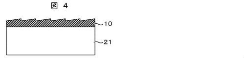
- FIG. 4 is a conceptual diagram of a cross section of a conventional diffraction grating replica.
- a conventional replica of a diffraction grating has a microstructure 10 made of resin on the surface of a glass substrate 21.
- the fine structure 10 has, for example, a shape in which the height of the bottom and top of the concavo-convex surface is about 0.1 ⁇ m, and the concavo-convex portions are periodically or randomly arranged at intervals of 0.1 ⁇ m to 10 ⁇ m. .
- the shape and size of the concavo-convex pattern of the fine structure 10 are appropriately set according to the required characteristics of the diffraction grating.
- a thickness of 10 mm is formed by forming a flat resin layer on the surface (back surface) opposite to the surface on which the fine structure of the glass substrate is formed.
- the inventors have found that a diffraction grating having a surface accuracy of ⁇ / 2 or less can be realized even when a glass substrate thinner than that and having a surface accuracy larger than ⁇ / 2 is used.
- the measurement surface and the optical flat plate are combined, and the surface is He— It is obtained by estimating from a Newton ring observed by irradiating Ne laser light.
- FIG. 1 is a sectional view of a replica of a diffraction grating according to an embodiment of the present invention.
- the diffraction grating according to the present embodiment has a microstructure comprising a glass substrate 20 having a thickness of 0.5 mm to 8 mm and a resin having a concavo-convex pattern formed on one surface of the glass substrate. 10 and a flat resin layer 30 formed on the other surface of the glass substrate.
- the flat resin layer 30 formed on the other surface of the glass substrate even if the surface accuracy of the glass substrate 20 is larger than ⁇ / 2, the fine structure 10 is obtained due to the flatness of the resin layer 30.
- the glass substrate 20 Is not affected by the surface accuracy of the glass substrate 20, and a diffraction grating having excellent surface accuracy can be obtained.
- a glass substrate having a surface accuracy larger than ⁇ / 2 can be used as the glass substrate to be used, a glass substrate having a thickness of 8 mm or less that is thinner than the conventional one can be used.
- the thickness of the glass substrate is preferably thinner from the viewpoint of miniaturization and weight reduction, and is preferably 3 mm or less from the viewpoint of imparting flexibility.
- the glass substrate has a role of supporting the fine structure 10 since it cannot maintain the shape of the surface by itself.
- the glass substrate has sufficient rigidity so that the glass substrate does not bend due to its own weight, and is preferably thicker than 0.5 mm. Therefore, the thickness of the glass substrate 20 is preferably in the range of 0.5 mm to 8 mm, and more preferably in the range of 1 mm to 3 mm. Further, the surface accuracy of the glass substrate 20 can be larger than ⁇ / 2, and a general-purpose glass plate called float glass or a glass plate that has been subjected to polishing can be used. Moreover, in order to improve the adhesiveness with the resin microstructure 10 or the resin layer 30, a glass plate having a satin finish on the surface can be used.
- the thickness of the fine structure 10 only needs to have a thickness capable of forming a predetermined concavo-convex pattern. For example, it may have a thickness of about 100 nm to 300 ⁇ m.
- the thickness of the resin layer 30 is not particularly limited as long as the flatness can be ensured.
- the resin layer 30 may have a thickness of about 100 nm to 300 ⁇ m.
- As the size of the diffraction grating a square or rectangular shape having a side of about 20 mm to 140 mm is generally used.
- the photocurable resin flows through the gaps between the glass substrate 20 and the master 1 and the optical flat plate 5, the photocurable resin 40 is filled in the uneven pattern of the master 1, and the photocurable resin 41 is the optical flat plate.
- a flat layer is formed along the surface.
- the UV curable resin 40, 41 is cured by simultaneously irradiating the UV curable resin 40, 41 with UV light with a UV lamp 50.
- the master 1 and the optical flat plate 5 are peeled off from the cured photocurable resin, respectively, so that the fine structure 10 is formed on one surface of the glass substrate 20 and the other surface is formed.
- a diffraction grating in which the flat resin layer 30 is formed can be manufactured.
- the optical flat plate 5 has a very excellent surface accuracy (for example, ⁇ / 10 or less)
- the photo-curing resin that is pressed and cured by the optical flat plate 5 is used.
- 41 resin layer 30
- the surface accuracy of the fine structure 10 formed on the glass substrate 20 is improved, and a diffraction grating of ⁇ / 2 or less can be realized. That is, by interposing a resin layer between the optical flat plate and the glass substrate 20, the surface accuracy of the fine structure 10 can be reproduced in the same manner as the optical flat plate, and an excellent surface accuracy diffraction grating can be realized.
- the surface accuracy of the diffraction grating to be manufactured can be made equal to the surface accuracy of the optical flat plate in addition to the advantage that the surface accuracy of the glass substrate 20 is eliminated.
- the surface accuracy of the diffraction grating can be set to ⁇ / 10 or less.
- a diffraction grating with high resolution can be provided.
- the optical flat plate is not a member used directly for the replica, the influence on the cost of the replica is small, and a diffraction grating having excellent surface accuracy can be obtained at a low cost.
- an optical flat is used as the pressurizing plate, but a plate other than the optical flat may be used as long as the surface accuracy is ⁇ / 2 or less.
- An advantage of the process shown in FIG. 2 is that the curing treatment by UV irradiation can be simultaneously performed on the photocurable resins 40 and 41 before curing.
- a photo-curing resin has a property of shrinking in volume before and after curing, which is called curing shrinkage.
- the curing treatment shown in FIG. 2 (c) is performed separately for the photocurable resins 40 and 41 in terms of time, the shrinkage of the photocurable resin that has been previously cured by the previously cured photocurable resin. It becomes easy to be affected.
- the stress applied to the front and back surfaces of the glass substrate 20 can be made uniform and canceled. As a result, the warp of the glass substrate 20 can be suppressed.
- the glass substrate 20 is curved to generate a peeling starting point between the master 1 and the photocurable resin, and is necessary for peeling both of them. Power can be reduced.
- the master 1 and the optical flat plate 5 are peeled at the same time in FIG. 2D. However, if necessary, the master 1 and the optical flat plate 5 may be peeled separately.
- the microstructure 10 and the resin layer 30 may be formed by a thermal nano-implement method.
- a film made of a thermoplastic resin is placed on both sides of the glass substrate, and the film is deformed along the shape of the master and the optical flat plate by softening the film by heating and pressing it with the master and the optical flat plate. Then, the film is cooled, and the master and the optical flat plate are peeled off from the film, whereby a diffraction grating replica can be produced.
- the thermal nanoimprint method residual stress due to thermal stress is likely to be generated in each member by the heating and cooling processes. From this viewpoint, the microstructure 10 and the resin layer 30 are formed using the optical nanoimprint method. It is preferable.
- the layers made of resin are arranged on both surfaces of the glass substrate 20, thereby warping more than the case where the resin layer (fine structure 10) is formed only on one surface shown in FIG. 1. Can be reduced.
- the microstructure 10 is formed by optical nanoimprinting, stress is partially generated by the curing shrinkage of the photocurable resin as described above, and warpage is likely to occur.
- the stress of curing shrinkage becomes symmetrical between the upper and lower surfaces of the glass substrate, and the warpage can be reduced.
- the microstructure 10 when the microstructure 10 is formed by thermal nanoimprinting, stress due to a difference in thermal expansion coefficient between the resin and the glass substrate is generated by the heating and cooling processes, and warpage is likely to occur.
- the stress due to the difference in thermal expansion coefficient is symmetric between the upper and lower surfaces of the glass substrate, and warpage can be reduced.
- the amount of curing shrinkage or the coefficient of thermal expansion of the resin constituting the microstructure 10 and the resin layer 30 is the same.
- the effect which suppresses curvature can be heightened by making the thickness of resin of both surfaces of the glass substrate 20 the same in this case.
- the structure in which the fine structure 10 made of a resin is formed on the surface of the glass substrate 20 has been described as a replica of the diffraction grating.
- a metal film such as aluminum, silver, or gold is formed on the surface of the fine structure 10. Is used in a state of being deposited by vapor deposition or the like.
- the thickness of the film is desirably 100 nm to 500 nm, which is a thickness that allows the light to be measured to be totally reflected and does not lose the shape of the microstructure.
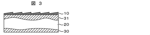
- FIG. 3 shows a cross-sectional view of the replica of the diffraction grating of the present embodiment.
- the resin layer formed on the concave / convex pattern forming surface side of the glass substrate 20 has a two-layer structure of the fine structure 10 and the resin layer 31.
- flat resin layers 30 and 31 having a surface accuracy of ⁇ / 2 or less are formed on both surfaces of the glass substrate 20 having a surface accuracy larger than ⁇ / 2, and the fine structure 10 is formed on the surface. It is in having formed. Even in such a configuration, a replica of a diffraction grating having excellent surface accuracy can be manufactured regardless of the surface accuracy of the glass substrate 20.
- the replica of the diffraction grating of this embodiment can be manufactured by applying the process shown in FIG. First, the process of forming the resin layers 30 and 31 on both surfaces of the glass substrate 20 will be described. This step is performed by replacing the master 1 with an optical flat plate in the process shown in FIG. That is, the glass substrate 20 to which the photocurable resin is supplied on both sides is pressed between a pair of optical flat plates and pressed, and the photocurable resins on both sides are cured with UV light, so that the pair of optical flat plates are resinized. By peeling from the layer, a laminated structure in which flat resin layers 30 and 31 are formed on both surfaces of the glass substrate 20 is obtained.
- the laminated structure in which the photocurable resin is supplied to the surface of the resin layer 31 is placed on the optical flat plate, the master 1 is pressed against the surface of the photocurable resin, and the photocurable resin is applied to the uneven pattern of the master 1. Then, the photocurable resin is cured with UV light, and the master 1 is peeled from the photocurable resin, whereby a replica of the diffraction grating shown in FIG. 3 can be produced.
- a metal layer is formed on the surface of the replica microstructure 10 produced in the same manner as in the first embodiment, and is used as a diffraction grating.
- the surface accuracy is reduced to a required value or less. It becomes possible.
- the cost of the diffraction grating can be reduced because the work of polishing the substrate glass that has been required can be simplified.
- the peeling process at the time of replica production can be facilitated by applying a thin glass substrate.
Landscapes
- Engineering & Computer Science (AREA)
- Physics & Mathematics (AREA)
- Mechanical Engineering (AREA)
- Manufacturing & Machinery (AREA)
- General Physics & Mathematics (AREA)
- Optics & Photonics (AREA)
- Health & Medical Sciences (AREA)
- Ophthalmology & Optometry (AREA)
- Diffracting Gratings Or Hologram Optical Elements (AREA)
Abstract
本発明は、面精度に優れ、小型、軽量化が可能な回折格子、および、その製造方法を提供することを目的とする。 本発明の回折格子は、厚さが0.5mm~8mmのガラス基板20と、ガラス基板20の一方の面に形成された凹凸パターンを有する樹脂からなる微細構造体10と、ガラス基板20の他方の面に形成された平坦な樹脂層30とを有することを特徴とする。ガラス基板20の面精度がλ/2よりも大きい場合でも、樹脂層30の平坦性によって、微細構造体10がガラス基板20の面精度の影響を受けず、面精度に優れた回折格子のレプリカが作製できる。また、ガラス基板を薄くできるため、回折格子の小型、軽量化を図ることができる。
Description
本発明は回折格子とその製造方法に関するものである。
分光器は、あるサンプルが発する光のスペクトルを分析する機器である。回折格子は分光器の基幹部品の一つである。分光器の性能は、回折格子の性能によって決まる。回折格子の性能を決めるものは、分析する光の波長と合わせた溝の間隔とその間隔の精度、分析する光の反射率、そして回折格子の面の凹凸の大きさを表す面精度である。
分光器で使用される回折格子は、ルーリングエンジンや電子ビーム照射装置を使用して金属片を切削して作製する。このような装置を利用した回折格子の作製は、それら装置の導入コストと維持コストが掛かるため、回折格子の量産には不向きである。
汎用品の分光器に使用する回折格子には、上記作製方法で作製した回折格子をマスターにして作製したレプリカを用いる。マスターからレプリカを取る作製方法は、ルーリングエンジンや電子ビーム照射装置の導入コストと維持コストを削減できるために、汎用品の分光器に使用する回折格子の作製方法に対して適している。
近年、ナノインプリント技術が発展し、様々な製品へ適用が始まっている。ナノインプリント技術とは、数ナノメートルサイズから数マイクロメートルの大きさの微細構造を、マスターからレプリカへ、或いはレプリカからレプリカへ転写する技術である。ナノインプリント技術は様々な製品へ適用できるという意味で汎用性が高い。また、ナノインプリント技術には自動化によって低コスト・大量生産を可能する技術も含まれる。このようなナノインプリント技術の適用によって、低コスト且つ大量の回折格子のレプリカ作製が可能となる(例えば、特許文献1等)。
ナノインプリント技術を用いた回折格子のレプリカ作製は、ガラス基板の表面に樹脂層を形成し、この樹脂層に原版(マスター)を押し付けて樹脂層に原版の反転パターンを転写し、樹脂層から原版を剥離することで行われる。ここで、回折格子の性能は面精度の影響を大きく受ける。一般的に回折格子としては、He-Neレーザーの光の波長(λ=632.8nm)を基準とする面精度がλ/2以下であることが必要とされ、このような面精度を満たすレプリカ作製が要求される。回折格子のレプリカ作製においては、作製されたレプリカの面精度はガラス基板の面精度の影響を受けるため、面精度に優れたガラス基板を用いる必要があった。しかしながら、面精度に優れるガラス基板は加工上の問題からある程度の厚みを有するガラスとなり、また、研磨加工の作業のためにコストが高いという課題を有していた。
回折格子のレプリカとして面精度の劣る薄いガラス基板を適用できれば、回折格子の小型化、軽量化、低コスト化の観点から好ましい。また、転写プロセスでの剥離プロセスを容易にするためにも、容易に湾曲できる薄いガラス基板を用いることが好ましい。しかしながら、このような面精度の劣る薄いガラス基板を用いて回折格子のレプリカを作製した場合には、回折格子の面精度も低下してしまい、所望のデバイス特性を得ることができなかった。
本発明は、面精度に優れ、小型、軽量化が可能な回折格子、および、その製造方法を提供することを目的とする。
[規則91に基づく訂正 24.04.2013]
本発明は、ガラス基板の表面に凹凸パターンを有する微細構造体が形成された回折格子の製造方法において、面精度がλ/2以下の平板上に、両面に光硬化性樹脂が供給された厚さが0.5mm~8mmのガラス基板を配置する工程と、両面に光硬化性樹脂が塗布された前記ガラス基板を、前記平板と凹凸パターンを有する原盤で挟んで加圧し、前記原盤と対向する光硬化性樹脂を前記原盤の凹凸パターンに充填する工程と、前記光硬化性樹脂を硬化する工程と、前記ガラス基板上の光硬化性樹脂から剥離することで、前記ガラス基板の一方の面に凹凸パターンを有する微細構造体と、他方の面に平坦な樹脂層を形成する工程と、を有することを特徴とするものである。
本発明は、ガラス基板の表面に凹凸パターンを有する微細構造体が形成された回折格子の製造方法において、面精度がλ/2以下の平板上に、両面に光硬化性樹脂が供給された厚さが0.5mm~8mmのガラス基板を配置する工程と、両面に光硬化性樹脂が塗布された前記ガラス基板を、前記平板と凹凸パターンを有する原盤で挟んで加圧し、前記原盤と対向する光硬化性樹脂を前記原盤の凹凸パターンに充填する工程と、前記光硬化性樹脂を硬化する工程と、前記ガラス基板上の光硬化性樹脂から剥離することで、前記ガラス基板の一方の面に凹凸パターンを有する微細構造体と、他方の面に平坦な樹脂層を形成する工程と、を有することを特徴とするものである。
[規則91に基づく訂正 24.04.2013]
また、ガラス基板の表面に凹凸パターンを有する微細構造体が形成された回折格子の製造方法において、両面に第一の光硬化性樹脂が供給された厚さが0.5mm~8mmのガラス基板を、面精度がλ/2以下の1対の平板上で挟んで加圧し、前記第一の光硬化性樹脂を硬化させて前記ガラス基板の両面に樹脂層を形成する工程と、前記ガラス基板の一方の樹脂層の表面に第二の光硬化性樹脂を供給し、前記第二の光硬化性樹脂に凹凸パターンを有する原盤を押し付けて、前記第二の光硬化性樹脂を前記原盤の凹凸パターンに充填する工程と、前記第二の光硬化性樹脂を硬化する工程と、前記第二の光硬化性樹脂から光硬化性樹脂から剥離することで、前記ガラス基板の一方の面に凹凸パターンを有する微細構造体を形成する工程と、を有することを特徴とするものである。
また、ガラス基板の表面に凹凸パターンを有する微細構造体が形成された回折格子の製造方法において、両面に第一の光硬化性樹脂が供給された厚さが0.5mm~8mmのガラス基板を、面精度がλ/2以下の1対の平板上で挟んで加圧し、前記第一の光硬化性樹脂を硬化させて前記ガラス基板の両面に樹脂層を形成する工程と、前記ガラス基板の一方の樹脂層の表面に第二の光硬化性樹脂を供給し、前記第二の光硬化性樹脂に凹凸パターンを有する原盤を押し付けて、前記第二の光硬化性樹脂を前記原盤の凹凸パターンに充填する工程と、前記第二の光硬化性樹脂を硬化する工程と、前記第二の光硬化性樹脂から光硬化性樹脂から剥離することで、前記ガラス基板の一方の面に凹凸パターンを有する微細構造体を形成する工程と、を有することを特徴とするものである。
また、本発明の回折格子は、厚さが0.5mm~8mmのガラス基板と、前記ガラス基板の一方の面に形成された凹凸パターンを有する樹脂からなる微細構造体と、前記ガラス基板の他方の面に形成された平坦な樹脂層とを有することを特徴とするものである。
なお、本明細書において、面精度とは特に断りのない限り、He-Neレーザーの光の波長(λ=632.8nm)を基準として求められる面精度を意味する。
本発明により、面精度に優れ、小型、軽量化が可能な回折格子、および、その製造方法が提供される。
まず、従来の回折格子のレプリカを説明する。図4に従来の回折格子のレプリカの断面の概念図を示す。図4に示すように、従来の回折格子のレプリカは、ガラス基板21の表面に樹脂で構成される微細構造体10を有するものである。微細構造体10は、例えば、凹凸面の底部と上部の高さが0.1μm前後で、凹凸部が0.1μm~10μmの間隔で周期的に或いはランダムに配置した形状を備えたものである。微細構造体10の凹凸パターンの形状、サイズは回折格子の要求特性等に応じて適宜設定される。ガラス基板21としては、He-Neレーザーの光の波長(λ=632.8nm)を基準とする面精度がλ/2以下を満たすものが使用され、ガラス基板21の厚さは10mm以上であった。
従来の構成では、厚さが10mmよりも薄いガラス基板を適用しようとした場合、回折格子の面精度をλ/2以下とすることが困難であった。これは、厚さが10mmよりも薄いガラス基板では面精度がλ/2よりも大きくなるためである。ガラス基板上に形成される微細構造体10は、ガラス基板21の面精度の影響を大きく受けるため、ガラス基板21の面精度がλ/2よりも大きくなると結果的に回折格子の面精度もλ/2よりも大きくなってしまうためである。
これに対して、本発明では回折格子のレプリカ作製において、ガラス基板の微細構造体が形成される面とは反対側の面(裏面)に平坦な樹脂層を形成することにより、厚さが10mmよりも薄く、面精度がλ/2よりも大きいガラス基板を用いた場合にも、面精度がλ/2以下の回折格子を実現できること見出し、発明に至ったものである。
なお、本発明において、面精度は、He-Neレーザーの光の波長(λ=632.8nm)を基準として測定されたものであり、測定面とオプティカルフラットプレートを合わせて、その面にHe-Neレーザーの光を照射して観測したニュートンリングから見積ることにより求められる。
以下、本発明の回折格子の実施形態について説明する。
(第1の実施形態)
図1に本発明の実施形態に係る回折格子のレプリカの断面図を示す。図1に示したように、本実施形態の回折格子は、厚さが0.5mm~8mmのガラス基板20と、ガラス基板の一方の面に形成された凹凸パターンを有する樹脂からなる微細構造体10と、ガラス基板の他方の面に形成された平坦な樹脂層30を備えている。ここで、ガラス基板の他方の面に形成された平坦な樹脂層30を設けることによって、ガラス基板20の面精度がλ/2よりも大きくても樹脂層30の平坦性によって、微細構造体10がガラス基板20の面精度の影響を受けることがなく、面精度に優れた回折格子とすることができる。これにより、使用するガラス基板としては、面精度がλ/2よりも大きいものを使用できるため、従来よりも厚さの薄い8mm以下のガラス基板を使用することができる。また、ガラス基板の厚さは小型、軽量化の観点からはより薄いことが好ましく、柔軟性付与の観点から3mm以下とすることが好ましい。一方、ガラス基板は、微細構造体10がそれ単体では面の形状を維持できないので、それを支える役目がある。そのため、少なくとも自重でガラス基板が湾曲しない程度の剛性を有している必要があり、0.5mmよりも厚いことが好ましい。よって、ガラス基板20の厚さとしては、0.5mm~8mmの範囲であることが好ましく、1mm~3mmの範囲とすることがより望ましい。また、ガラス基板20の面精度としては、λ/2よりも大きいものを使用でき、フロートガラスと呼ばれる汎用のガラス板や、研磨加工が施されてガラス板などを用いることができる。また、樹脂の微細構造体10や樹脂層30との密着性の向上を図るために、表面に梨地加工を施したガラス板を用いることもできる。微細構造体10の厚さとしては、所定の凹凸パターンを形成できる厚さを有していれば良く、例えば、100nm~300μm程度の厚さを有していればよい。また、樹脂層30の厚さとしては、平坦性を確保できる厚さがあればよく、例えば、100nm~300μm程度の厚さを有していればよい。回折格子の大きさとしては、正方形、長方形の形状で一辺が20mm~140mm程度のものが一般的に用いられる。
図1に本発明の実施形態に係る回折格子のレプリカの断面図を示す。図1に示したように、本実施形態の回折格子は、厚さが0.5mm~8mmのガラス基板20と、ガラス基板の一方の面に形成された凹凸パターンを有する樹脂からなる微細構造体10と、ガラス基板の他方の面に形成された平坦な樹脂層30を備えている。ここで、ガラス基板の他方の面に形成された平坦な樹脂層30を設けることによって、ガラス基板20の面精度がλ/2よりも大きくても樹脂層30の平坦性によって、微細構造体10がガラス基板20の面精度の影響を受けることがなく、面精度に優れた回折格子とすることができる。これにより、使用するガラス基板としては、面精度がλ/2よりも大きいものを使用できるため、従来よりも厚さの薄い8mm以下のガラス基板を使用することができる。また、ガラス基板の厚さは小型、軽量化の観点からはより薄いことが好ましく、柔軟性付与の観点から3mm以下とすることが好ましい。一方、ガラス基板は、微細構造体10がそれ単体では面の形状を維持できないので、それを支える役目がある。そのため、少なくとも自重でガラス基板が湾曲しない程度の剛性を有している必要があり、0.5mmよりも厚いことが好ましい。よって、ガラス基板20の厚さとしては、0.5mm~8mmの範囲であることが好ましく、1mm~3mmの範囲とすることがより望ましい。また、ガラス基板20の面精度としては、λ/2よりも大きいものを使用でき、フロートガラスと呼ばれる汎用のガラス板や、研磨加工が施されてガラス板などを用いることができる。また、樹脂の微細構造体10や樹脂層30との密着性の向上を図るために、表面に梨地加工を施したガラス板を用いることもできる。微細構造体10の厚さとしては、所定の凹凸パターンを形成できる厚さを有していれば良く、例えば、100nm~300μm程度の厚さを有していればよい。また、樹脂層30の厚さとしては、平坦性を確保できる厚さがあればよく、例えば、100nm~300μm程度の厚さを有していればよい。回折格子の大きさとしては、正方形、長方形の形状で一辺が20mm~140mm程度のものが一般的に用いられる。
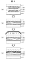
次に、図2を用いて、図1に示した回折格子の作製方法を説明する。図2はナノインプリント技術を用いて回折格子のレプリカを作製した例である。ここでは、光ナノインプリト法により微細構造体10を形成した例である。まず、図2(a)に示すように、ガラス基板20の一方の面に微細構造体10を形成するための光硬化性樹脂40、他方面に平坦な樹脂層30を形成するための光硬化性樹脂41を供給する。次に、図2(b)に示すように、凹凸パターンを有する原盤1とオプティカルフラットプレート5で、光硬化性樹脂40/ガラス基板20/光硬化性樹脂41を挟み、加圧する。この工程で、ガラス基板20と原盤1、オプティカルフラットプレート5の隙間を光硬化性樹脂が流動し、光硬化性樹脂40は原盤1の凹凸パターンに充填され、光硬化性樹脂41はオプティカルフラットプレートに面に沿った平坦層を形成する。この状態で、図2(c)に示すようにUVランプ50でUV光を硬化前の光硬化性樹脂40、41に同時に照射することで、光硬化性樹脂40、41を硬化させる。その後、図2(d)に示すように、硬化した光硬化性樹脂から原盤1、オプティカルフラットプレート5をそれぞれ剥離することによって、ガラス基板20の一方の面に微細構造体10、他方の面に平坦な樹脂層30が形成された回折格子を作製することができる。
図2に示したレプリカ作製において、オプティカルフラットプレート5が非常に優れた面精度(例えば、λ/10以下)を有しているため、オプティカルフラットプレート5によって加圧され、硬化した光硬化性樹脂41(樹脂層30)はオプティカルフラットプレート5に対応した優れた面精度を有する。その結果、ガラス基板20上に形成された微細構造体10の面精度も向上し、λ/2以下の回折格子を実現することができる。すなわち、オプティカルフラットプレートとガラス基板20の間に樹脂層を介在させることで、微細構造体10の面精度をオプティカルフラットプレートと同じように再現でき、優れた面精度の回折格子を実現できる。このことは、ガラス基板20の面精度の制限が無くなることというメリットの他に、作製される回折格子の面精度をオプティカルフラットプレートの面精度と同等の値にすることが可能になるという利点を有する。つまり、回折格子の面精度をλ/10以下とすることも可能となる。これによって、分解能の高い回折格子を提供することができる。図1に示した従来の構成では、面精度λ/10以下を実現するためにはそれに対応したガラス基板を使用する必要があり、レプリカのコストが非常に高くなる。一方、本実施形態では、オプティカルフラットプレートはレプリカに直接使用する部材ではないため、レプリカのコストへの影響は小さく、低コストで面精度に優れた回折格子を得ることできる。なお、ここでは加圧用のプレートとして、オプティカルフラットを用いた例を示したが、面精度がλ/2以下であればオプティカルフラット以外のプレートを使用することも可能である。
図2に示したプロセスの利点として、UV照射による硬化処理を硬化前の光硬化性樹脂40、41に対して同時に行えることが挙げられる。一般的に光硬化樹脂は、硬化収縮と呼ばれる硬化前後で体積収縮する特性を持つ。図2(c)に示す硬化処理を光硬化性樹脂40と41に対して時間的に別々に行うと、先に硬化処理した光硬化性樹脂が後で硬化処理した光硬化性樹脂の硬化収縮の影響を受けやすくなる。同時に硬化処理を行うことで、ガラス基板20の表面と裏面にかかる応力を均等にし、打ち消すことができる。結果、ガラス基板20の反りを抑えることができる。
図2(d)に示す剥離工程では、薄いガラス基板20を使用すれば、ガラス基板20を湾曲させることで原盤1と光硬化性樹脂との間に剥離起点が発生し、両者の剥離に必要な力を低減することができる。剥離の手順は、図2(d)では、原盤1とオプティカルフラットプレート5の剥離を同時に行っているが、必要であれば原盤1とオプティカルフラットプレート5を別々に剥離しても良い。また剥離を容易にするために、図2(a)に示す工程の前に、原盤1とオプティカルフラットプレート5に予め、離型剤と呼ばれるフッ素系材料からなる溶液を塗布しておくことが望ましい。
図2に示した作製例では、光硬化性樹脂を用いた光ナノインプリト法を用いた例を示したが、熱ナノインプリト法によって微細構造体10および樹脂層30を形成しても良い。この場合、ガラス基板の両面に熱可塑性樹脂からなるフィルムを配置し、加熱によってフィルムを軟化させて原盤およびオプティカルフラットプレートで加圧することによって、原盤およびオプティカルフラットプレートの形状に沿ってフィルムを変形させた後、フィルムを冷却し、原盤およびオプティカルフラットプレートをフィルムから剥離することで、回折格子のレプリカを作製することができる。なお、熱ナノインプリント法では加熱、冷却工程によって、各部材に熱応力に起因する残留応力が生成されやすく、このような観点からは光ナノインプリント法を用いて微細構造体10および樹脂層30を形成することが好ましい。
本実施形態の回折格子では、ガラス基板20の両面に樹脂からなる層が配置されることにより、図1に示した片面のみに樹脂層(微細構造体10)が形成された場合よりも反りを低減することができる。光ナノインプリントにより微細構造体10を形成した場合には、上述のように光硬化性樹脂の硬化収縮によって部分的に応力が発生し、反りが発生しやすくなる。これに対して、両面に樹脂層があることで、硬化収縮の応力がガラス基板の上下面で対称となり、反りを低減できる。また、熱ナノインプリントにより微細構造体10を形成した場合には、加熱、冷却工程によって、樹脂とガラス基板の熱膨張率差による応力が発生し、反りが発生しやすくなる。この場合も同様に両面に樹脂層があることで、熱膨張率差による応力がガラス基板の上下面で対称となり、反りを低減できる。このため、反りを低減する観点からは、微細構造体10および樹脂層30を構成する樹脂の硬化収縮量あるいは熱膨張率が同じであることが好ましい。また、この際、ガラス基板20の両面の樹脂の厚さを同じとすることで、反りを抑える効果を高めることができる。
回折格子のレプリカとして、ガラス基板20の表面に樹脂からなる微細構造体10が形成された構造について説明したが、回折格子としては、微細構造体10の表面にアルミニウム、銀又は金などの金属膜を蒸着等で成膜した状態で使用される。成膜する厚さは、測定対象の光が全反射し、且つ、微細構造体の形状が失われない程度の厚さである100nm~500nmが望ましい。
(第2の実施形態)
本発明の実施形態に係る回折格子のレプリカの変形例を説明する。図3に本実施形態の回折格子のレプリカの断面図を示す。第一の実施形態との相違点は、ガラス基板20の凹凸パターン形成面側に形成される樹脂層を微細構造体10と樹脂層31の2層構造とした点である。本実施形態の特徴としては、面精度がλ/2よりも大きいガラス基板20の両面に面精度がλ/2以下となる平坦な樹脂層30、31を形成し、その表面に微細構造体10を形成したことにある。このような構成においても、ガラス基板20の面精度に関わらず、優れた面精度を有する回折格子のレプリカを作製することができる。
本発明の実施形態に係る回折格子のレプリカの変形例を説明する。図3に本実施形態の回折格子のレプリカの断面図を示す。第一の実施形態との相違点は、ガラス基板20の凹凸パターン形成面側に形成される樹脂層を微細構造体10と樹脂層31の2層構造とした点である。本実施形態の特徴としては、面精度がλ/2よりも大きいガラス基板20の両面に面精度がλ/2以下となる平坦な樹脂層30、31を形成し、その表面に微細構造体10を形成したことにある。このような構成においても、ガラス基板20の面精度に関わらず、優れた面精度を有する回折格子のレプリカを作製することができる。
本実施形態の回折格子のレプリカは、図2に示すプロセスを応用して作製することができる。まず、ガラス基板20の両面に樹脂層30、31を形成する工程を説明する。この工程は、図2に示したプロセスにおいて、原盤1をオプティカルフラットプレートに置き換えて行う。すなわち、光硬化性樹脂が両面に供給されたガラス基板20を1対のオプティカルフラットプレートで挟んで加圧し、UV光により両面の光硬化性樹脂を硬化させて、1対のオプティカルフラットプレートを樹脂層から剥離することで、ガラス基板20の両面に平坦な樹脂層30、31が形成された積層構造体を得る。その後、樹脂層31の表面に光硬化性樹脂が供給された積層構造体をオプティカルフラットプレート上に配置し、光硬化性樹脂の表面に原盤1を押し付け、光硬化性樹脂を原盤1の凹凸パターンに充填した後、UV光により光硬化性樹脂を硬化し、原盤1を光硬化性樹脂から剥離することで、図3に示す回折格子のレプリカを作製することができる。
第一の実施形態と同様に作製したレプリカの微細構造体10の表面に金属層が成膜され、回折格子として使用される。
以上で説明した第1、第2の実施形態によれば、面精度が少なくともλ/2以下が要求される回折格子のレプリカ作製において、薄いガラス基板を用いても面精度を要求値以下にすることが可能となる。これにより、従来、困難であった薄いガラス基板を使用することが可能となり、回折格子の軽量化を図ることができる。さらには、これまで必要であった基板ガラスへの研磨加工の作業を簡略できることから回折格子のコストを削減することができる。また、薄いガラス基板を適用することでレプリカ作製時の剥離プロセスを容易にできる。
1 原盤
5 オプティカルフラットプレート
10 微細構造体
20、21 ガラス基板
30、31 樹脂層
40、41 光硬化性樹脂
50 UVランプ
5 オプティカルフラットプレート
10 微細構造体
20、21 ガラス基板
30、31 樹脂層
40、41 光硬化性樹脂
50 UVランプ
Claims (10)
- [規則91に基づく訂正 24.04.2013]
ガラス基板の表面に凹凸パターンを有する微細構造体が形成された回折格子の製造方法において、
面精度がλ/2以下の平板上に、両面に光硬化性樹脂が供給された厚さが0.5mm~8mmのガラス基板を配置する工程と、
両面に光硬化性樹脂が塗布された前記ガラス基板を、前記平板と凹凸パターンを有する原盤で挟んで加圧し、前記原盤と対向する光硬化性樹脂を前記原盤の凹凸パターンに充填する工程と、
前記光硬化性樹脂を硬化する工程と、
前記ガラス基板上の光硬化性樹脂から剥離することで、前記ガラス基板の一方の面に凹凸パターンを有する微細構造体と、他方の面に平坦な樹脂層を形成する工程と、
を有することを特徴とする回折格子の製造方法。 - 請求項1において、前記ガラス基板の面精度がλ/2よりも大きいことを特徴とする回折格子の製造方法。
- 請求項1において、前記微細構造体の表面に金属層を形成する工程を有することを特徴とする回折格子の製造方法。
- [規則91に基づく訂正 24.04.2013]
ガラス基板の表面に凹凸パターンを有する微細構造体が形成された回折格子の製造方法において、
両面に第一の光硬化性樹脂が供給された厚さが0.5mm~8mmのガラス基板を、面精度がλ/2以下の1対の平板上で挟んで加圧し、前記第一の光硬化性樹脂を硬化させて前記ガラス基板の両面に樹脂層を形成する工程と、
前記ガラス基板の一方の樹脂層の表面に第二の光硬化性樹脂を供給し、前記第二の光硬化性樹脂に凹凸パターンを有する原盤を押し付けて、前記第二の光硬化性樹脂を前記原盤の凹凸パターンに充填する工程と、
前記第二の光硬化性樹脂を硬化する工程と、
前記第二の光硬化性樹脂から剥離することで、前記ガラス基板の一方の面に凹凸パターンを有する微細構造体を形成する工程と、を有することを特徴とする回折格子の製造方法。 - 請求項4において、前記ガラス基板の面精度がλ/2よりも大きいことを特徴とする回折格子の製造方法。
- 請求項5において、前記微細構造体の表面に金属層を形成する工程を有することを特徴とする回折格子の製造方法。
- 厚さが0.5mm~8mmのガラス基板と、前記ガラス基板の一方の面に形成された凹凸パターンを有する樹脂からなる微細構造体と、前記ガラス基板の他方の面に形成された平坦な樹脂層とを有することを特徴とする回折格子。
- 請求項7において、前記微細構造体の表面に金属層が形成されていることを特徴とする回折格子。
- 請求項7において、前記ガラス基板の面精度がλ/2よりも大きく、前記平坦な樹脂層の面精度がλ/2以下であることを特徴とする回折格子。
- 請求項9において、前記微細構造体が2層構造の樹脂層で構成されていることを特徴とする回折格子。
Priority Applications (3)
| Application Number | Priority Date | Filing Date | Title |
|---|---|---|---|
| CN201380007879.6A CN104094140B (zh) | 2012-03-30 | 2013-02-01 | 衍射光栅及其制造方法 |
| EP13768255.5A EP2808709B1 (en) | 2012-03-30 | 2013-02-01 | Method for manufacturing a diffraction grating |
| US14/379,974 US9261631B2 (en) | 2012-03-30 | 2013-02-01 | Method for manufacturing a diffraction grating |
Applications Claiming Priority (2)
| Application Number | Priority Date | Filing Date | Title |
|---|---|---|---|
| JP2012078806A JP5965698B2 (ja) | 2012-03-30 | 2012-03-30 | 回折格子およびその製造方法 |
| JP2012-078806 | 2012-03-30 |
Publications (1)
| Publication Number | Publication Date |
|---|---|
| WO2013145850A1 true WO2013145850A1 (ja) | 2013-10-03 |
Family
ID=49259135
Family Applications (1)
| Application Number | Title | Priority Date | Filing Date |
|---|---|---|---|
| PCT/JP2013/052302 WO2013145850A1 (ja) | 2012-03-30 | 2013-02-01 | 回折格子およびその製造方法 |
Country Status (5)
| Country | Link |
|---|---|
| US (1) | US9261631B2 (ja) |
| EP (1) | EP2808709B1 (ja) |
| JP (1) | JP5965698B2 (ja) |
| CN (1) | CN104094140B (ja) |
| WO (1) | WO2013145850A1 (ja) |
Cited By (1)
| Publication number | Priority date | Publication date | Assignee | Title |
|---|---|---|---|---|
| US10261223B2 (en) | 2014-01-31 | 2019-04-16 | Canon Usa, Inc. | System and method for fabrication of miniature endoscope using nanoimprint lithography |
Families Citing this family (6)
| Publication number | Priority date | Publication date | Assignee | Title |
|---|---|---|---|---|
| JP6188743B2 (ja) | 2014-06-19 | 2017-08-30 | キヤノン株式会社 | 複数の光学機能面を有する光学素子、分光装置およびその製造方法 |
| RU2642139C1 (ru) * | 2016-12-27 | 2018-01-24 | Акционерное общество "Научно-производственное объединение "Государственный институт прикладной оптики" (АО "НПО ГИПО") | Способ изготовления дифракционных решеток |
| JP7060370B2 (ja) * | 2017-12-18 | 2022-04-26 | 株式会社ミツトヨ | スケールおよびその製造方法 |
| JP7330280B2 (ja) * | 2019-02-22 | 2023-08-21 | ビュージックス コーポレーション | 平行板導波路 |
| JP7345954B2 (ja) * | 2019-08-14 | 2023-09-19 | エルジー・ケム・リミテッド | 回折導光板および回折導光板の製造方法 |
| CN113009609A (zh) * | 2021-03-01 | 2021-06-22 | 苏州大学 | 体光栅标定组件、体光栅的制备装置、标定方法和曝光方法 |
Citations (7)
| Publication number | Priority date | Publication date | Assignee | Title |
|---|---|---|---|---|
| JPS61209139A (ja) * | 1985-03-14 | 1986-09-17 | Victor Co Of Japan Ltd | 情報記録媒体基盤の製作法 |
| JPS6318254B2 (ja) * | 1980-07-18 | 1988-04-18 | Sony Corp | |
| JPH05185441A (ja) * | 1992-01-09 | 1993-07-27 | Fujitsu Ltd | 樹脂層複製方法 |
| JPH09274425A (ja) * | 1996-04-03 | 1997-10-21 | Sekinosu Kk | ホログラム素子およびその製造方法 |
| JPH10232306A (ja) * | 1997-02-20 | 1998-09-02 | Canon Inc | 回折光学素子の製造方法 |
| JP2003315519A (ja) * | 2002-04-18 | 2003-11-06 | Dainippon Printing Co Ltd | 複製用版材 |
| JP2007323762A (ja) | 2006-06-02 | 2007-12-13 | Epson Toyocom Corp | 回折格子とその製造方法、及び光ピックアップ装置 |
Family Cites Families (10)
| Publication number | Priority date | Publication date | Assignee | Title |
|---|---|---|---|---|
| US3337945A (en) * | 1965-06-30 | 1967-08-29 | Bausch & Lomb | Method of forming diffraction grating masters ruled in transfer films |
| DE2936854A1 (de) * | 1979-09-12 | 1981-04-02 | Robert Bosch Gmbh, 7000 Stuttgart | Verfahren zum herstellen eines gegenstandes mit einer aus kunstharz bestehenden oberflaeche |
| JP2512706B2 (ja) * | 1985-05-27 | 1996-07-03 | 日立マクセル株式会社 | 光情報記録媒体およびその製造方法 |
| JPS62238502A (ja) * | 1986-04-09 | 1987-10-19 | Toshiba Corp | グレ−テイングレンズ |
| JPS62238503A (ja) | 1986-04-10 | 1987-10-19 | Toshiba Corp | グレ−テイングレンズ |
| JPH02202330A (ja) * | 1989-01-30 | 1990-08-10 | Hitachi Ltd | 車両用交流発電機 |
| US5225935A (en) | 1989-10-30 | 1993-07-06 | Sharp Kabushiki Kaisha | Optical device having a microlens and a process for making microlenses |
| JPH08248207A (ja) * | 1995-03-10 | 1996-09-27 | Omron Corp | 光学素子及び光学素子の製造方法並びに画像表示装置 |
| JP2006084885A (ja) * | 2004-09-17 | 2006-03-30 | Shimadzu Corp | レプリカ回折格子の製造方法 |
| JP2007101799A (ja) * | 2005-10-03 | 2007-04-19 | Nippon Sheet Glass Co Ltd | 透過型光学素子 |
-
2012
- 2012-03-30 JP JP2012078806A patent/JP5965698B2/ja not_active Expired - Fee Related
-
2013
- 2013-02-01 CN CN201380007879.6A patent/CN104094140B/zh not_active Expired - Fee Related
- 2013-02-01 EP EP13768255.5A patent/EP2808709B1/en not_active Not-in-force
- 2013-02-01 US US14/379,974 patent/US9261631B2/en not_active Expired - Fee Related
- 2013-02-01 WO PCT/JP2013/052302 patent/WO2013145850A1/ja active Application Filing
Patent Citations (7)
| Publication number | Priority date | Publication date | Assignee | Title |
|---|---|---|---|---|
| JPS6318254B2 (ja) * | 1980-07-18 | 1988-04-18 | Sony Corp | |
| JPS61209139A (ja) * | 1985-03-14 | 1986-09-17 | Victor Co Of Japan Ltd | 情報記録媒体基盤の製作法 |
| JPH05185441A (ja) * | 1992-01-09 | 1993-07-27 | Fujitsu Ltd | 樹脂層複製方法 |
| JPH09274425A (ja) * | 1996-04-03 | 1997-10-21 | Sekinosu Kk | ホログラム素子およびその製造方法 |
| JPH10232306A (ja) * | 1997-02-20 | 1998-09-02 | Canon Inc | 回折光学素子の製造方法 |
| JP2003315519A (ja) * | 2002-04-18 | 2003-11-06 | Dainippon Printing Co Ltd | 複製用版材 |
| JP2007323762A (ja) | 2006-06-02 | 2007-12-13 | Epson Toyocom Corp | 回折格子とその製造方法、及び光ピックアップ装置 |
Non-Patent Citations (1)
| Title |
|---|
| See also references of EP2808709A4 |
Cited By (1)
| Publication number | Priority date | Publication date | Assignee | Title |
|---|---|---|---|---|
| US10261223B2 (en) | 2014-01-31 | 2019-04-16 | Canon Usa, Inc. | System and method for fabrication of miniature endoscope using nanoimprint lithography |
Also Published As
| Publication number | Publication date |
|---|---|
| JP5965698B2 (ja) | 2016-08-10 |
| CN104094140A (zh) | 2014-10-08 |
| EP2808709A4 (en) | 2015-05-13 |
| US9261631B2 (en) | 2016-02-16 |
| JP2013210419A (ja) | 2013-10-10 |
| EP2808709B1 (en) | 2016-04-20 |
| CN104094140B (zh) | 2016-08-24 |
| EP2808709A1 (en) | 2014-12-03 |
| US20150015957A1 (en) | 2015-01-15 |
Similar Documents
| Publication | Publication Date | Title |
|---|---|---|
| JP5965698B2 (ja) | 回折格子およびその製造方法 | |
| CN116256829A (zh) | 一种近眼显示器衍射光栅波导的制备方法 | |
| TWI730185B (zh) | 結構的微影製造 | |
| KR101020634B1 (ko) | 기능성 나노패턴을 갖는 렌즈의 제조방법 | |
| JP4811032B2 (ja) | 反射型レプリカ光学素子 | |
| EP3631534B1 (en) | Method of manufacturing a diffractive grating | |
| JP6510548B2 (ja) | 曲面回折格子の型の製造方法、曲面回折格子の製造方法、曲面回折格子、および光学装置 | |
| JP2001235611A (ja) | ホログラフィック・グレーティング | |
| TW201410588A (zh) | 表面增強拉曼散射元件之製造方法 | |
| US20090267245A1 (en) | Transmission Type Optical Element | |
| TWI665078B (zh) | 製造圖案化印模以圖案化輪廓表面之方法、供在壓印微影製程中使用之圖案化印模、壓印微影方法、包括圖案化輪廓表面之物件及圖案化印模用於壓印微影之用法 | |
| JP5838777B2 (ja) | 成形用型の製造方法 | |
| WO2020021989A1 (ja) | 凹面回折格子の製造方法、製造装置及び凹面回折格子 | |
| JP2020522023A (ja) | 高さ調整された光回折格子を製造する方法 | |
| JP5349777B2 (ja) | 光学素子の製造方法 | |
| KR20180066307A (ko) | 플라즈모닉 메타표면 제작방법 | |
| JP5066815B2 (ja) | 反射型回折格子 | |
| KR20110140059A (ko) | 나노 임프린트용 스탬프 및 이의 제조 방법 | |
| JP2002040220A (ja) | 回折格子 | |
| JP7500588B2 (ja) | インプリントモールドの製造方法、インプリントモールド、モールドブランク、及び光学素子の製造方法 | |
| JP2006084885A (ja) | レプリカ回折格子の製造方法 | |
| JP2016035977A (ja) | インプリント用モールドとインプリント方法およびワイヤーグリッド偏光子とその製造方法 | |
| CN113156761A (zh) | 一种嵌合式压印模板及其制作方法 | |
| US20220082935A1 (en) | Nanostamping Method and Nano-Optical Component | |
| JP2013193454A (ja) | マスターモールドの製造方法およびモールドの製造方法並びにそれらに使用される表面加工方法 |
Legal Events
| Date | Code | Title | Description |
|---|---|---|---|
| 121 | Ep: the epo has been informed by wipo that ep was designated in this application |
Ref document number: 13768255 Country of ref document: EP Kind code of ref document: A1 |
|
| WWE | Wipo information: entry into national phase |
Ref document number: 2013768255 Country of ref document: EP |
|
| WWE | Wipo information: entry into national phase |
Ref document number: 14379974 Country of ref document: US |
|
| NENP | Non-entry into the national phase |
Ref country code: DE |