WO2013145692A1 - 表示装置、電子機器及びタッチパネル - Google Patents
表示装置、電子機器及びタッチパネル Download PDFInfo
- Publication number
- WO2013145692A1 WO2013145692A1 PCT/JP2013/002008 JP2013002008W WO2013145692A1 WO 2013145692 A1 WO2013145692 A1 WO 2013145692A1 JP 2013002008 W JP2013002008 W JP 2013002008W WO 2013145692 A1 WO2013145692 A1 WO 2013145692A1
- Authority
- WO
- WIPO (PCT)
- Prior art keywords
- touch panel
- terminal
- wiring
- terminals
- layer
- Prior art date
- Legal status (The legal status is an assumption and is not a legal conclusion. Google has not performed a legal analysis and makes no representation as to the accuracy of the status listed.)
- Ceased
Links
Images



Classifications
-
- G—PHYSICS
- G06—COMPUTING OR CALCULATING; COUNTING
- G06F—ELECTRIC DIGITAL DATA PROCESSING
- G06F3/00—Input arrangements for transferring data to be processed into a form capable of being handled by the computer; Output arrangements for transferring data from processing unit to output unit, e.g. interface arrangements
- G06F3/01—Input arrangements or combined input and output arrangements for interaction between user and computer
- G06F3/03—Arrangements for converting the position or the displacement of a member into a coded form
- G06F3/041—Digitisers, e.g. for touch screens or touch pads, characterised by the transducing means
- G06F3/0416—Control or interface arrangements specially adapted for digitisers
- G06F3/04164—Connections between sensors and controllers, e.g. routing lines between electrodes and connection pads
-
- G—PHYSICS
- G06—COMPUTING OR CALCULATING; COUNTING
- G06F—ELECTRIC DIGITAL DATA PROCESSING
- G06F1/00—Details not covered by groups G06F3/00 - G06F13/00 and G06F21/00
- G06F1/16—Constructional details or arrangements
- G06F1/1613—Constructional details or arrangements for portable computers
- G06F1/1633—Constructional details or arrangements of portable computers not specific to the type of enclosures covered by groups G06F1/1615 - G06F1/1626
- G06F1/1637—Details related to the display arrangement, including those related to the mounting of the display in the housing
- G06F1/1643—Details related to the display arrangement, including those related to the mounting of the display in the housing the display being associated to a digitizer, e.g. laptops that can be used as penpads
-
- G—PHYSICS
- G06—COMPUTING OR CALCULATING; COUNTING
- G06F—ELECTRIC DIGITAL DATA PROCESSING
- G06F3/00—Input arrangements for transferring data to be processed into a form capable of being handled by the computer; Output arrangements for transferring data from processing unit to output unit, e.g. interface arrangements
- G06F3/01—Input arrangements or combined input and output arrangements for interaction between user and computer
- G06F3/03—Arrangements for converting the position or the displacement of a member into a coded form
- G06F3/041—Digitisers, e.g. for touch screens or touch pads, characterised by the transducing means
- G06F3/0412—Digitisers structurally integrated in a display
-
- H—ELECTRICITY
- H04—ELECTRIC COMMUNICATION TECHNIQUE
- H04M—TELEPHONIC COMMUNICATION
- H04M1/00—Substation equipment, e.g. for use by subscribers
- H04M1/02—Constructional features of telephone sets
- H04M1/0202—Portable telephone sets, e.g. cordless phones, mobile phones or bar type handsets
- H04M1/026—Details of the structure or mounting of specific components
- H04M1/0266—Details of the structure or mounting of specific components for a display module assembly
-
- H—ELECTRICITY
- H05—ELECTRIC TECHNIQUES NOT OTHERWISE PROVIDED FOR
- H05K—PRINTED CIRCUITS; CASINGS OR CONSTRUCTIONAL DETAILS OF ELECTRIC APPARATUS; MANUFACTURE OF ASSEMBLAGES OF ELECTRICAL COMPONENTS
- H05K1/00—Printed circuits
- H05K1/18—Printed circuits structurally associated with non-printed electric components
- H05K1/189—Printed circuits structurally associated with non-printed electric components characterised by the use of flexible or folded printed circuits
-
- G—PHYSICS
- G06—COMPUTING OR CALCULATING; COUNTING
- G06F—ELECTRIC DIGITAL DATA PROCESSING
- G06F2203/00—Indexing scheme relating to G06F3/00 - G06F3/048
- G06F2203/041—Indexing scheme relating to G06F3/041 - G06F3/045
- G06F2203/04107—Shielding in digitiser, i.e. guard or shielding arrangements, mostly for capacitive touchscreens, e.g. driven shields, driven grounds
-
- G—PHYSICS
- G06—COMPUTING OR CALCULATING; COUNTING
- G06F—ELECTRIC DIGITAL DATA PROCESSING
- G06F3/00—Input arrangements for transferring data to be processed into a form capable of being handled by the computer; Output arrangements for transferring data from processing unit to output unit, e.g. interface arrangements
- G06F3/01—Input arrangements or combined input and output arrangements for interaction between user and computer
- G06F3/03—Arrangements for converting the position or the displacement of a member into a coded form
- G06F3/041—Digitisers, e.g. for touch screens or touch pads, characterised by the transducing means
- G06F3/044—Digitisers, e.g. for touch screens or touch pads, characterised by the transducing means by capacitive means
- G06F3/0446—Digitisers, e.g. for touch screens or touch pads, characterised by the transducing means by capacitive means using a grid-like structure of electrodes in at least two directions, e.g. using row and column electrodes
-
- H—ELECTRICITY
- H05—ELECTRIC TECHNIQUES NOT OTHERWISE PROVIDED FOR
- H05K—PRINTED CIRCUITS; CASINGS OR CONSTRUCTIONAL DETAILS OF ELECTRIC APPARATUS; MANUFACTURE OF ASSEMBLAGES OF ELECTRICAL COMPONENTS
- H05K2201/00—Indexing scheme relating to printed circuits covered by H05K1/00
- H05K2201/03—Conductive materials
- H05K2201/0302—Properties and characteristics in general
-
- H—ELECTRICITY
- H05—ELECTRIC TECHNIQUES NOT OTHERWISE PROVIDED FOR
- H05K—PRINTED CIRCUITS; CASINGS OR CONSTRUCTIONAL DETAILS OF ELECTRIC APPARATUS; MANUFACTURE OF ASSEMBLAGES OF ELECTRICAL COMPONENTS
- H05K2201/00—Indexing scheme relating to printed circuits covered by H05K1/00
- H05K2201/10—Details of components or other objects attached to or integrated in a printed circuit board
- H05K2201/10007—Types of components
- H05K2201/10128—Display
-
- H—ELECTRICITY
- H05—ELECTRIC TECHNIQUES NOT OTHERWISE PROVIDED FOR
- H05K—PRINTED CIRCUITS; CASINGS OR CONSTRUCTIONAL DETAILS OF ELECTRIC APPARATUS; MANUFACTURE OF ASSEMBLAGES OF ELECTRICAL COMPONENTS
- H05K2201/00—Indexing scheme relating to printed circuits covered by H05K1/00
- H05K2201/10—Details of components or other objects attached to or integrated in a printed circuit board
- H05K2201/10007—Types of components
- H05K2201/10151—Sensor
Definitions
- the present invention relates to a display device, an electronic device, and a touch panel, and more particularly, to a display device including a touch panel, an electronic device including the display device, and a touch panel.
- a display device provided with a touch panel is configured to be operable by touching, for example, an icon displayed on the display screen via the touch panel.
- the display apparatus provided with the touch panel is mounted in the mobile phone in recent years, and attracts attention as a multifunctional smart phone.
- reduction in thickness and weight is demanded. For example, by sharing a part of a plurality of glass substrates constituting a display panel, a touch panel, etc. A configuration in which the number of glass substrates is reduced has been proposed.
- Patent Document 1 discloses an electronic device that includes a touch panel in which a touch detection electrode is provided on the back side of a cover substrate that protects a display screen, and a liquid crystal display panel that is provided on the touch panel via an adhesive layer. It is disclosed. Patent Document 1 describes that according to this electronic device, the cover substrate that protects the surface and the glass substrate that constitutes the touch panel are shared, so that the electronic device can be thinned. .
- the touch panel has a terminal area in which a plurality of terminals are arranged.
- an FPC Flexible Printed Circuit
- ACF Anisotropic Conductive
- Film Anisotropic conductive film
- the cover substrate is a substrate that can be visually recognized by the user.
- a configuration in which a frame-shaped shielding layer is arranged on the outer peripheral portion including the terminal region around the sensor region where the touched (detected) position can be detected has become mainstream. Therefore, even if the indentation inspection described above is performed after the FPC is pressure-bonded to the touch panel layer provided on the back side of the cover substrate, the shielding layer is provided in the terminal region, so that the conductive particles contained in the ACF are crushed. It is difficult to check the condition. If it becomes so, it will become difficult to ensure the reliability of connection by ACF at the time of crimping
- substrate is a substrate that can be visually recognized by the user.
- This invention is made
- the place made into the objective is a flexible printed wiring board (in the touch panel layer of a cover board
- ACF anisotropic conductive film
- the present invention provides a pair of second terminals connected to each other in the terminal area of the touch panel layer of the cover substrate, and one end of the flexible printed wiring board is connected to one second terminal.
- a second wiring having the other end grounded is provided, and a third wiring having one end connected to the other second terminal and the other end reaching the external connection side is provided.
- a display device is provided with a cover substrate having a frame-shaped shielding layer on the outer periphery, a sensor region on the inside of the shielding layer, and an outer side of the sensor region.
- a touch panel layer with terminal areas defined at the end of the board; a flexible printed circuit board that is crimped to the terminal areas of the touch panel layer with an anisotropic conductive film; and the touch panel layer side of the cover board.
- a display panel provided via a transparent adhesive layer and having a display area disposed so as to overlap the sensor area, wherein the touch panel layer is provided so as to be aligned with each other in the terminal area.
- the wiring board has one end connected to each of the first terminals and the other end connected to the external connection side, and one end connected to the one second terminal. And a second wiring provided so that the other end is grounded, and a third wiring provided so that one end is connected to the other second terminal and the other end reaches the external connection side And.
- the plurality of first terminals respectively drawn from the sensor area and the pair of second terminals connected to each other are provided in the terminal area (of the touch panel layer) of the cover substrate on which the shielding layer is arranged. It is provided so that it may line up mutually.
- the flexible printed wiring board has one end connected to each first terminal and the other end connected to the first terminal, and the other end connected to one second terminal. And a second wiring having the other end grounded and a third wiring having one end connected to the other second terminal and the other end reaching the external connection side.
- each first terminal provided in the terminal area of the touch panel layer of the cover substrate includes a pair of second terminals provided in the terminal region of the touch panel layer of the cover substrate and the flexible printed wiring board. It may be considered that the state of electrical connection with the provided second wiring and third wiring is substantially the same.
- the second wiring provided on the flexible printed wiring board (the other end is grounded), the pair of second terminals connected to each other provided in the terminal region of the touch panel layer of the cover substrate, and the flexible
- the third wiring provided on the flexible printed wiring board is electrically connected in series if the flexible printed wiring board is normally crimped to the terminal area of the touch panel layer.
- Provided in the terminal region of the touch panel layer of the cover substrate by measuring the electrical resistance between the external connection side of the third wiring provided on the wiring board and, for example, the ground electrode provided in the inspection device or the like The state of electrical connection between the pair of second terminals and the second wiring and the third wiring provided on the flexible printed wiring board is confirmed.
- the state of electrical connection between each first terminal provided in the terminal area of the touch panel layer of the cover substrate and each first wiring provided on the flexible printed wiring board can be inferred. Even if a shielding layer is provided on the outer periphery of the substrate, the cover substrate provided with the touch panel layer by measuring the electrical resistance using the external connection side of the third wiring provided on the flexible printed wiring board (Touch panel) In the manufacturing line of the display device provided with the display panel, the reliability of connection by the anisotropic conductive film when the flexible printed wiring board is pressure-bonded to the touch panel layer of the cover substrate is ensured.
- the side to be crimped to the terminal region is formed in two branches, the second wiring is provided in one of the two branches, and the third wiring is provided in the other of the two branches. Good.
- the second wiring is provided on one of the portions formed on the forked portion of the flexible printed wiring board, and the third wiring is provided on the other. Therefore, the flexible printed wiring board is provided on the flexible printed wiring board.
- the pair of second terminals may be connected to each other via an outer peripheral wiring provided so as to surround the sensor region.
- one of the pair of second terminals is grounded via the second wiring, and the pair of second terminals is connected to each other via the outer peripheral wiring provided so as to surround the sensor region.
- the outer peripheral wiring is also grounded, and for example, the destruction of the wiring pattern provided in the sensor region due to electrostatic discharge (ESD) is suppressed.
- the touch panel layer may include an outer peripheral wiring provided to surround the sensor region and be grounded.
- the touch panel layer includes the outer peripheral wiring provided so as to surround the sensor region and be grounded.
- the wiring pattern provided in the sensor region is prevented from being damaged by electrostatic discharge.
- the display panel is a liquid crystal display panel, and a backlight is provided on a side opposite to the cover substrate of the display panel, and an inner end of the outer peripheral wiring is located outside a peripheral end of the backlight. May be provided.
- the inner end of the outer peripheral wiring to be grounded is provided so as to be outside the peripheral end of the backlight, a built-in deviation occurs between the liquid crystal display panel and the backlight.
- the outer peripheral wiring protrudes from the assembly of the liquid crystal display panel and the backlight, and for example, the destruction of the wiring pattern provided in the sensor region due to electrostatic discharge is further suppressed.
- the touch panel layer includes a plurality of first transparent wiring patterns provided to extend in parallel with each other in the sensor region, and a plurality of touch panel layers provided to extend in parallel with each other in a direction intersecting with the first transparent wiring patterns.
- the second transparent wiring pattern and an insulating film provided between the plurality of first transparent wiring patterns and the plurality of second transparent wiring patterns may be provided.
- the touch panel layer includes a plurality of first transparent wiring patterns extending in parallel with each other in the sensor region, and a plurality of second transparent wiring patterns extending in parallel with each other in a direction intersecting with each first transparent wiring pattern. And an insulating film that electrically insulates between the plurality of first transparent wiring patterns and the plurality of second transparent wiring patterns, the projection capacitive touch panel is specifically configured on the touch panel layer. Is done.
- an electronic device includes any one of the display devices described above.
- a pair of 2nd terminal connected mutually is provided in the terminal area
- connection reliability by an anisotropic conductive film is secured when a flexible printed wiring board is pressure-bonded to a touch panel layer of a cover substrate.
- the touch panel according to the present invention includes a cover substrate having a frame-shaped shielding layer provided on an outer peripheral portion, a sensor region provided inside the shielding layer, and a substrate end outside the sensor region.
- Touch panel layers each having a terminal area defined therein, and a flexible printed wiring board crimped to the terminal area of the touch panel layer through an anisotropic conductive film, and the touch panel layer is provided on the terminal area.
- a plurality of first terminals provided so as to be aligned with each other and drawn from the sensor region, and a pair of second terminals provided so as to be aligned with the plurality of first terminals and connected to each other.
- the printed wiring board has a plurality of first wirings provided such that one end is connected to each of the first terminals and the other end extends to the external connection side, and one end is A second wiring provided so as to be connected to one second terminal and the other end grounded, and one end connected to the other second terminal and the other end reaching the external connection side. And a third wiring provided as described above.
- the plurality of first terminals respectively drawn from the sensor area and the pair of second terminals connected to each other are provided in the terminal area (of the touch panel layer) of the cover substrate on which the shielding layer is arranged. It is provided so that it may line up mutually.
- the flexible printed wiring board has one end connected to each first terminal and the other end connected to the first terminal, and the other end connected to one second terminal. And a second wiring having the other end grounded and a third wiring having one end connected to the other second terminal and the other end reaching the external connection side.
- each first terminal provided in the terminal area of the touch panel layer of the cover substrate includes a pair of second terminals provided in the terminal region of the touch panel layer of the cover substrate and the flexible printed wiring board. It may be considered that the state of electrical connection with the provided second wiring and third wiring is substantially the same.
- the second wiring provided on the flexible printed wiring board (the other end is grounded), the pair of second terminals connected to each other provided in the terminal region of the touch panel layer of the cover substrate, and the flexible
- the third wiring provided on the flexible printed wiring board is electrically connected in series if the flexible printed wiring board is normally crimped to the terminal area of the touch panel layer.
- Provided in the terminal region of the touch panel layer of the cover substrate by measuring the electrical resistance between the external connection side of the third wiring provided on the wiring board and, for example, the ground electrode provided in the inspection device or the like The state of electrical connection between the pair of second terminals and the second wiring and the third wiring provided on the flexible printed wiring board is confirmed.
- the state of electrical connection between each first terminal provided in the terminal area of the touch panel layer of the cover substrate and each first wiring provided on the flexible printed wiring board can be inferred. Even if a shielding layer is provided on the outer periphery of the substrate, the cover substrate can be used in the touch panel production line by measuring the electrical resistance using the external connection side of the third wiring provided on the flexible printed wiring board. The reliability of the connection by the anisotropic conductive film when the flexible printed wiring board is pressure-bonded to the touch panel layer is ensured.
- a pair of second terminals connected to each other are provided in the terminal region of the touch panel layer of the cover substrate, one end of the flexible printed wiring board is connected to one second terminal, and the other end is A second wiring to be grounded is provided, and a third wiring is provided with one end connected to the other second terminal and the other end reaching the external connection side. Even if the shielding layer is provided, it is possible to ensure the reliability of connection by the anisotropic conductive film when the flexible printed wiring board is pressure-bonded to the touch panel layer of the cover substrate.
- FIG. 1 is a perspective view of the electronic apparatus according to the first embodiment.
- FIG. 2 is a cross-sectional view of a display device constituting the electronic apparatus according to the first embodiment.
- FIG. 3 is a cross-sectional view of a sensor substrate constituting the display device according to the first embodiment.
- FIG. 4 is a plan view of the sensor substrate according to the first embodiment.
- FIG. 5 is a plan view of a touch panel constituting the display device according to the first embodiment.
- FIG. 6 is a plan view of the touch panel according to the second embodiment.
- FIG. 7 is a plan view relating to the first mode of the touch panel according to the third embodiment.
- FIG. 8 is a plan view relating to a second aspect of the touch panel according to the third embodiment.
- FIG. 9 is a plan view relating to a third aspect of the touch panel according to the third embodiment.
- Embodiment 1 of the Invention 1 to 5 show Embodiment 1 of a display device, an electronic device, and a touch panel according to the present invention.
- FIG. 1 is a perspective view of the smartphone 60 of the present embodiment.
- FIG. 2 is a cross-sectional view of the liquid crystal display device 50 that constitutes the smartphone 60.
- FIG. 3 is a sectional view of the sensor substrate 20 constituting the liquid crystal display device 50.
- FIG. 4 is a plan view of the sensor substrate 20.
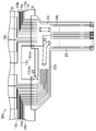
- FIG. 5 is a plan view of an end portion of the touch panel 30a constituting the liquid crystal display device 50.
- FIG. 1 is a perspective view of the smartphone 60 of the present embodiment.
- FIG. 2 is a cross-sectional view of the liquid crystal display device 50 that constitutes the smartphone 60.
- FIG. 3 is a sectional view of the sensor substrate 20 constituting the liquid crystal display device 50.
- FIG. 4 is a plan view of the sensor substrate 20.
- FIG. 5 is a plan view of an
- the smartphone 60 is provided with a liquid crystal display device 50 (see FIG. 2) provided such that a display region D for displaying an image is exposed from a thin housing 55 whose upper side in the drawing is rectangular. Is an electronic device.
- the display area D and an outer portion along one short side (lower left side in the drawing) of the display area D are overlapped.
- a sensor region S in which the touch position can be detected is defined.
- the liquid crystal display device 50 includes a touch panel 30a, a liquid crystal display panel 40 provided on the lower side of the touch panel 30a via an adhesive layer 23, and a lower side of the liquid crystal display panel 40 in the figure. And a backlight 45 provided.
- the touch panel 30 a includes a sensor substrate 20, an FPC 22 a that is pressure-bonded to an end portion (terminal region T described later) of the sensor substrate 20 via an ACF 21, and a touch panel controller 29 that is mounted on the FPC 22 a It has.
- the sensor substrate 20 is provided so as to cover the cover layer 10 made of glass, the shielding layer 11 provided in a frame shape on the cover substrate 10, and the shielding layer 11.
- a plurality of second transparent wiring patterns 15a provided in the sensor region S on the insulating film 14 so as to extend in parallel to each other in the lateral direction in FIG.
- the outer peripheral wiring 15b provided so as to surround the sensor region S in the outer peripheral portion F outside the sensor region S on the insulating film 14, and the second transparent wiring pattern 15a and the second peripheral wiring 15b provided so as to cover the outer peripheral wiring 15b.
- a planarizing film 16 16
- an outer peripheral portion F in which the shielding layer 11 is provided around the sensor region S is defined.
- a terminal region T is defined along one side of the outer peripheral portion F.
- the shielding layer 11 provided around the sensor region S is omitted.
- the shielding layer 11 is made of, for example, a resin material in which a black pigment is dispersed.
- the first planarizing film 12, the insulating film 14, and the second planarizing film 16 are made of, for example, a colorless and transparent resin material.
- the plurality of first transparent wiring patterns 13 a are respectively drawn out to the terminal region T, and the terminal region T forms a plurality of transmission-side first terminals 13 at. Further, as shown in FIG. 5, the plurality of first transparent wiring patterns 13a are drawn out in two places in accordance with the shape of the FPC 22a formed at the fork to be described later. One terminal 13at is also provided in two locations. Then, on the right side of the group of the first transmission side first terminals (13at, see FIG. 4) in FIG. 5, one second terminal 13cta is provided alongside each transmission side first terminal 13at. Further, the other second terminal 13ctb is provided on the left side of the group of the first transmission side first terminals (13at, see FIG. 4) in FIG. 5 alongside each transmission side first terminal 13at.
- the pair of second terminals 13cta and 13ctb are connected to each other via the outer peripheral wiring 13c.
- the plurality of second transparent wiring patterns 15 a are drawn to the right side and the left side of the terminal region T in the drawing, and become a plurality of reception-side first terminals 15 at in the terminal region T.
- the pair of ground wiring patterns 13 b are drawn out to the right and left sides of the terminal region T in the drawing, and the terminal region T forms a pair of ground terminals 13 bt.
- the outer peripheral wiring 15 b is drawn out to the right and left sides of the terminal region T in the drawing, and forms a pair of ground terminals 15 bt in the terminal region T. Further, the inner ends along the left side, the upper side, and the right side in FIG. 4 of the outer peripheral wiring 15 b are outside the peripheral end of the backlight 45.
- the width between the peripheral end of the sensor region S and the outer end of the outer peripheral wiring 15b is set within 2 mm.
- the first transparent wiring pattern 13a, the ground wiring pattern 13b, the outer peripheral wiring 13c, the second transparent wiring pattern 15a and the outer peripheral wiring 15b are made of a transparent conductive film such as an ITO (IndiumITOTin Oxide) film, for example. Further, in each lower layer of the first transparent wiring pattern 13a, the ground wiring pattern 13b, the outer peripheral wiring 13c, the second transparent wiring pattern 15a, and the outer peripheral wiring 15b, as shown in FIG. A metal layer 17 made of a low electrical resistance metal material is laminated.
- the shielding layer 11, the first planarizing film 12, the first transparent wiring pattern 13a, the transmission-side first terminal 13at, and the ground wiring pattern are formed on the cover substrate 10.
- the metal layer 17 is provided as the touch panel layer 18.
- the ACF 21 is obtained by dispersing conductive particles in a film such as a thermosetting epoxy resin.
- the FPC 22a includes, for example, a polyimide base film, a copper wiring pattern provided on the front and back surfaces of the base film, and a polyimide cover lay provided so as to cover each copper wiring pattern.
- the FPC 22a has one end connected to each ground terminal 15bt (see FIG. 4) on the sensor substrate 20 and the other end connected to the external connection side. And one end of the ground wiring 23 provided so as to reach the transmission side first terminal 13at (see FIG. 4) and each reception side first terminal 15at (see FIG. 4) on the sensor substrate 20.
- the other end extends to the external connection side and is connected to the plurality of first wires 24a provided so as to reach the touch panel controller 29, and one end is connected to the second terminal 13cta on the sensor substrate 20, respectively.
- the second wiring 25 provided so that the other end is grounded, one end is connected to the second terminal 13ctb on the sensor substrate 20, and the other end reaches the external connection side.
- a plurality of external connection wirings 27 having one end connected to the touch panel controller 29 and the other end reaching the external connection side.
- the FPC 22a has a bifurcated side on the terminal region T of the sensor substrate 20, and a second wiring 25 is provided on one of the bifurcated sides (the left side in the figure).
- the third wiring 26 is provided on the other side (the right side in the figure).
- the touch panel controller 29 side is illustrated by an abstract arrow.
- the adhesive layer 23 is made of, for example, an optically colorless and transparent double-sided tape or an adhesive.
- the liquid crystal display panel 40 includes, for example, a TFT (Thin Film Transistor) substrate 35 and a CF (Color Filter) substrate 36 provided so as to face each other, and between the TFT substrate 35 and the CF substrate 36.
- a liquid crystal layer (not shown) provided on the TFT substrate 35 and the CF substrate 36 are bonded to each other, and a sealing material (not shown) is provided for sealing the liquid crystal layer between the TFT substrate 35 and the CF substrate 40.
- an LSI (Large Scale Integration) 46 for driving is mounted on the terminal region of the TFT substrate 35 protruding from the CF substrate 36.
- polarizing plates are attached to the front surface (for example, the surface on the CF substrate 36 side) and the back surface (for example, the surface on the TFT substrate 35 side) of the liquid crystal display panel 40, respectively.
- the backlight 45 includes, for example, a thin housing having an open top surface, a flat light guide plate provided inside the housing, a plate-shaped reflection sheet provided on the bottom surface of the light guide plate, A plurality of light sources such as LEDs (Light Emitting Diodes) disposed inside the light guide plate and a substantially half-divided tube disposed inside the housing and disposed so as to surround the plurality of light sources And an optical sheet such as a lens sheet or a diffusion sheet provided on the upper surface of the light guide plate.
- LEDs Light Emitting Diodes
- the smartphone 60 configured as described above transmits the liquid crystal display panel 40 from the backlight 45 by applying a predetermined voltage to each sub-pixel, which is the minimum unit of an image, on the liquid crystal layer between the TFT substrate 35 and the CF substrate 36.
- a predetermined voltage to each sub-pixel, which is the minimum unit of an image, on the liquid crystal layer between the TFT substrate 35 and the CF substrate 36.
- the touch panel controller 29 is configured to calculate and detect a touch position based on a change in capacitance generated at the intersection.
- the manufacturing method of the liquid crystal display device 50 constituting the smartphone 60 of the present embodiment includes a liquid crystal display panel manufacturing process, a touch panel manufacturing process, a panel pasting process, and a backlight incorporation process.
- a TFT substrate (35) and a CF substrate (36) are respectively produced using a well-known method.
- the TFT substrate (35) and the CF substrate (36) are produced using an ODF (One Drop Fill) method.
- ODF One Drop Fill
- the glass substrates constituting the TFT substrate (35) and the CF substrate (36) are thinned to produce the liquid crystal display panel 40.
- polarizing plates are attached to the front and back surfaces of the liquid crystal display panel 40.
- the collapse state of the conductive particles contained in the ACF is checked from the surface opposite to the surface where the drive circuit 46 and the FPC are pressure-bonded. The reliability of connection by ACF is ensured by performing an indentation inspection.
- ⁇ Touch panel manufacturing process> First, on the cover substrate 10, using a known method, the shielding layer 11, the first planarizing film 12, the metal layer 17, the first transparent wiring pattern 13a, the transmission-side first terminal 13at, the ground wiring pattern 13b, the ground The terminal 13bt, the outer peripheral wiring 13c, the second terminals 13cta and 13ctb, the insulating film 14, the second transparent wiring pattern 15a, the receiving-side first terminal 15at, the outer peripheral wiring 15b, the ground terminal 15bt, and the second planarizing film 16 are sequentially formed. As a result, the sensor substrate 20 is manufactured.
- the FPC 22a on which the touch panel controller 29 is mounted is pressure-bonded to the terminal region T of the touch panel layer 18 of the manufactured sensor substrate 20 via the ACF 21, thereby manufacturing the touch panel 30a.
- the touch panel of the touch panel 30a is measured by measuring the electrical resistance between the external connection side of the third wiring 26 provided in the FPC 22a and the ground electrode provided in the inspection apparatus or the like. Check the electrical connection between the pair of second terminals 13cta and 13ctb provided in the terminal region T of the layer 18 and the second wiring 25 and the third wiring 26 provided in the FPC 22a, and perform a touch panel preliminary inspection. To ensure the reliability of connection by the ACF 21.
- a bonded body is manufactured by bonding the liquid crystal display panel 40 subjected to the indentation inspection in the liquid crystal display panel manufacturing process and the touch panel 30a subjected to the touch panel preliminary inspection in the touch panel manufacturing process via the adhesive layer 23.
- a touch panel main inspection such as a lighting inspection of the liquid crystal display panel 40 and an accuracy inspection of the touch position of the touch panel 30a is performed.
- the liquid crystal display device 50 of the present embodiment can be manufactured.
- the sensor region S is included in the terminal region T (of the touch panel layer 18) of the cover substrate 10 on which the shielding layer 11 is disposed.
- a plurality of transmission-side first terminals 13at and a plurality of reception-side first terminals 15at, respectively, and a pair of second terminals 13cta and 13ctb connected to each other are provided so as to be aligned with each other.
- the FPC 22a has one end connected to each transmission side first terminal 13at and each reception side first terminal 15at and the other end extending to the external connection side to reach the touch panel controller 29.
- One wiring 24a one end connected to one second terminal 13cta and the other end grounded, and one end connected to the other second terminal 13ctb and the other end connected to the external connection side
- a third wiring 26 is provided to reach.
- the FPC 22a since the FPC 22a is pressure-bonded to the terminal region T of the touch panel layer 18 via the ACF 21, each transmission-side first terminal 13at and each reception provided in the terminal region T of the touch panel layer 18 of the cover substrate 10 are connected.
- the state of electrical connection between the first side terminal 15 at and each first wiring 24 a provided on the FPC 22 a is a pair of second terminals 13 cta and 13 ctb provided in the terminal region T of the touch panel layer 18 of the cover substrate 10.
- the state of electrical connection with the second wiring 25 and the third wiring 26 provided in the FPC 22a may be considered to be substantially the same.
- the second wiring 25 provided in the FPC 22a (the other end is grounded), a pair of second terminals 13cta and 13ctb connected to each other provided in the terminal region T of the touch panel layer 18 of the cover substrate 10, and Since the third wiring 26 provided in the FPC 22a is electrically connected in series if the FPC 22a is normally crimped to the terminal region T of the touch panel layer 18, the third wiring 26 provided in the FPC 22a.
- connection state can also be inferred, even if the shielding layer 11 is provided on the outer peripheral portion F of the cover substrate 10, the electrical resistance is measured using the external connection side of the third wiring 26 provided on the FPC 22a.
- the ACF 21 is used when the FPC 22a is pressure-bonded to the touch panel layer 18 of the cover substrate 10. Connection reliability can be ensured.
- the touch panel layer of the cover substrate 10 can be applied to both of the separated crimped portions of the FPC 22a formed by bifurcation only by measuring the electrical resistance using the external connection side of the third wiring 26 provided on the FPC 22a.
- the state of electrical connection between each transmission-side first terminal 13at and each reception-side first terminal 15at provided in the 18 terminal region T and each first wiring 24a provided in the FPC 22a can be analogized. .
- the touch panel layer 18 includes the outer peripheral wiring 15b provided so as to surround the sensor area S and be grounded. Breakdown due to electrostatic discharge of the first transparent wiring pattern 13a and the second transparent wiring pattern 15a provided in S can be suppressed.
- the inner end of the outer peripheral wiring 15b to be grounded is provided so as to be outside the peripheral end of the backlight 45. Even if a misalignment occurs between the display panel 40 and the backlight 45, only the outer peripheral wiring 15 b protrudes from the assembly of the liquid crystal display panel 40 and the backlight 45 and is provided in the sensor region S. In addition, the destruction of the first transparent wiring pattern 13a and the second transparent wiring pattern 15a due to electrostatic discharge can be further suppressed.
- FIG. 6 is a plan view of an end portion of the touch panel 30b of the present embodiment.
- the same parts as those in FIGS. 1 to 5 are denoted by the same reference numerals, and detailed description thereof is omitted.
- the touch panel 30a in which the touch panel controller 29 is mounted on the FPC 22a is illustrated, but in the present embodiment, the touch panel 30b in which the touch panel controller (29) is not mounted on the FPC 22b is illustrated.
- FPC 22b is provided so that one end is connected to each ground terminal 15bt (see FIG. 4) on sensor substrate 20 and the other end reaches the external connection side.
- the grounding wiring 23 is connected to each transmitting side first terminal 13at (see FIG. 4) and each receiving side first terminal 15at (see FIG. 4) on the sensor substrate 20, and the other end is external.
- a plurality of first wires 24b provided so as to extend to the connection side and reach the external connection side, respectively, one end is connected to the second terminal 13cta on the sensor substrate 20, and the other end is grounded.
- the terminal area T (of the touch panel layer 18) of the cover substrate 10 on which the shielding layer 11 is arranged has a plurality of transmissions drawn from the sensor area S, respectively.
- the side first terminal 13at, the plurality of reception side first terminals 15at, and the pair of second terminals 13cta and 13ctb connected to each other are arranged side by side.
- the FPC 22b has one end connected to each transmitting side first terminal 13at and each receiving side first terminal 15at, and the other end extending to the external connection side to reach the external connection side.
- One wiring 24b one end connected to one second terminal 13cta and the other end grounded, and one end connected to the other second terminal 13ctb and the other end connected to the external connection side
- a third wiring 26 is provided to reach.
- the FPC 22b is pressure-bonded to the terminal area T of the touch panel layer 18 via the ACF 21, each transmission-side first terminal 13at and each reception provided in the terminal area T of the touch panel layer 18 of the cover substrate 10 are provided.
- the state of electrical connection between the first side terminal 15 at and each first wiring 24 b provided on the FPC 22 b is determined by a pair of second terminals 13 cta and 13 ctb provided in the terminal region T of the touch panel layer 18 of the cover substrate 10.
- the state of electrical connection with the second wiring 25 and the third wiring 26 provided in the FPC 22b may be considered to be substantially the same.
- the second wiring 25 provided in the FPC 22b (the other end is grounded), a pair of second terminals 13cta and 13ctb connected to each other provided in the terminal region T of the touch panel layer 18 of the cover substrate 10, and
- the third wiring 26 provided in the FPC 22b is electrically connected in series if the FPC 22b is normally crimped to the terminal region T of the touch panel layer 18, and therefore the third wiring 26 provided in the FPC 22b.
- connection state can also be estimated, even if the shielding layer 11 is provided on the outer peripheral portion F of the cover substrate 10, the electrical resistance is measured using the external connection side of the third wiring 26 provided on the FPC 22b.
- the FPC 22b is pressure-bonded to the touch panel layer 18 of the cover substrate 10. The reliability of the connection by the ACF 21 can be ensured.
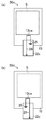
- FIG.7 (a) is a top view of the touch panel 30c of this embodiment
- FIG.7 (b) is a top view of the touch panel 30d of the modification
- FIG. 8A is a plan view of the touch panel 30e of the present embodiment
- FIG. 8B is a plan view of a touch panel 30f of the modification
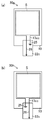
- Fig.9 (a) is a top view of the touch panel 30g of this embodiment
- FIG.8 (b) is a top view of the touchscreen 30h of the modification.
- a peripheral wiring 13ca that connects one second terminal (13cta) and the other second terminal (13ctb) to each other is a single FPC 22c on the cover substrate 10.
- the touch panel 30a of the first embodiment or the touch panel 30b of the second embodiment is the same as that of the touch panel 30a of the first embodiment. It is substantially the same.
- the touch panel 30d according to the modified example is obtained by horizontally inverting the configuration of the touch panel 30c.
- an outer peripheral wiring 13cb that connects one second terminal (13cta) and the other second terminal (13ctb) to each other is a single FPC 22c on the cover substrate 10.
- the touch panel 30a according to the first embodiment or the implementation described above is provided only in the area between the upper side in the figure formed in the figure and the lower side in the figure of the sensor area S and the area overlapping the FPC 22c. This is substantially the same as the touch panel 30b of the second embodiment.
- the touch panel 30f according to the modified example is obtained by horizontally inverting the configuration of the touch panel 30e.
- the outer peripheral wiring 13cc that connects the one second terminal (13cta) and the other second terminal (13ctb) to each other is formed on the cover substrate 10 in the sensor region S.
- the other configurations are substantially the same as those of the touch panel 30a of the first embodiment or the touch panel 30b of the second embodiment only by being provided along the periphery.
- the touch panel 30h according to the modification is obtained by horizontally inverting the configuration of the touch panel 30g.
- one of the pair of second terminals (13cta) is grounded via the second wiring 25, and the pair of second terminals 13cta and 13ctb is provided so as to surround the sensor region S. Since the outer peripheral wiring 13cc is connected to each other via the outer peripheral wiring 13cc, the outer peripheral wiring 13cc is also grounded, and the first transparent wiring pattern 13a and the second transparent wiring pattern 15a provided in the sensor region S are destroyed by electrostatic discharge. Can be suppressed. Further, the inner end of the outer peripheral wiring 13cc along the left side, the upper side and the right side in FIGS. 9A and 9B is outside the peripheral end of the backlight (45). Further, the width between the peripheral end of the sensor region S and the outer end of the outer peripheral wiring 13cc is set within 2 mm.
- the second terminals 13cta and 13ctb are provided, the FPC 22c is provided with a second wiring 25 having one end connected to one second terminal 13cta and the other end grounded, and one end being the other second terminal. Since the third wiring 26 connected to 13 ctb and having the other end reaching the external connection side is provided, the touch panel layer 18 of the cover substrate 10 is provided even if the shielding layer 11 is provided on the outer peripheral portion F of the cover substrate 10. It is possible to ensure the reliability of connection by the ACF 21 when the FPC 22c is pressure-bonded.
- a projected capacitive touch panel is illustrated, but the present invention can also be applied to other types of touch panels such as a surface capacitive touch panel and a resistive film touch panel.
- a liquid crystal display panel is exemplified as the display panel.
- the present invention can also be applied to other display panels such as an organic EL (Electro Luminescence) display panel.
- an organic EL Electro Luminescence
- the present invention is applied to a display device provided with an organic EL panel, a backlight is unnecessary, so that further thinning of the device can be realized.
- the touch panel provided with the glass cover substrate is illustrated, but the present invention can also be applied to a touch panel provided with a plastic cover substrate.
- a small electronic device for mobile use such as a mobile phone has been illustrated.
- the present invention can also be applied to a large electronic device such as an electronic blackboard.
- the connection reliability by the ACF can be ensured when the FPC is crimped to the touch panel layer of the cover substrate. This is useful for manufacturing mobile electronic devices that are required to be thin and light.
Landscapes
- Engineering & Computer Science (AREA)
- Theoretical Computer Science (AREA)
- General Engineering & Computer Science (AREA)
- Physics & Mathematics (AREA)
- General Physics & Mathematics (AREA)
- Human Computer Interaction (AREA)
- Computer Hardware Design (AREA)
- Computer Networks & Wireless Communication (AREA)
- Microelectronics & Electronic Packaging (AREA)
- Signal Processing (AREA)
- Liquid Crystal (AREA)
- Devices For Indicating Variable Information By Combining Individual Elements (AREA)
- Position Input By Displaying (AREA)
Abstract
カバー基板(10)のタッチパネル層の端子領域(T)に、センサー領域(S)からそれぞれ引き出された複数の第1端子、及び互いに接続された一対の第2端子(13cta、13ctb)が互いに並ぶように設けられ、FPC(22a)に、一方端が各第1端子にそれぞれ接続されると共に他方端が外部接続側にそれぞれ延びる複数の第1配線(24a)、一方端が一方の第2端子(13cta)に接続されると共に他方端が接地される第2配線(25)、及び一方端が他方の第2端子(13ctb)に接続されると共に他方端が外部接続側に到達する第3配線(26)が設けられている。
Description
本発明は、表示装置、電子機器及びタッチパネルに関し、特に、タッチパネルを備えた表示装置、その表示装置を備えた電子機器及びタッチパネルに関するものである。
タッチパネルを備えた表示装置は、例えば、表示画面に表示されたアイコンなどにタッチパネルを介して触れることにより、その操作が可能に構成されている。そして、タッチパネルを備えた表示装置は、近年、携帯電話機に搭載され、多機能なスマートフォンとして注目されている。ここで、携帯電話機などのモバイル用途の電子機器では、特に、薄型化及び軽量化が要望されているので、例えば、表示パネル及びタッチパネルなどを構成する複数のガラス基板の一部を共有することにより、ガラス基板の枚数を減らした構成が提案されている。
例えば、特許文献1には、表示画面を保護するカバー基板の裏面側にタッチ検出電極が設けられたタッチパネルと、そのタッチパネルに接着層を介して設けられた液晶表示パネルとを備えた電子機器が開示されている。そして、特許文献1には、この電子機器によれば、表面を保護するカバー基板とタッチパネルを構成するガラス基板とが共有されるので、電子機器を薄型化することができる、と記載されている。
ところで、タッチパネルは、複数の端子が配列された端子領域を有し、その端子領域には、外部回路などに接続するためのFPC(Flexible Printed Circuit:可撓性プリント配線板)がACF(Anisotropic Conductive Film:異方性導電フィルム)を介して圧着接続されている。そして、実際の製造ラインでは、タッチパネルにFPCを圧着した後に、例えば、タッチパネルのFPCが圧着された表面と反対側の表面からACFに含まれる導電粒子の潰れ具合を偏光顕微鏡で観察する圧痕検査と呼ばれる簡易的な検査を行うことにより、タッチパネルに設けられた各端子とFPCに設けられた各端子との間の電気的な接続を確認して、製造ラインにおけるACFによる接続の信頼性を確保することが有効になっている。
ここで、上記特許文献1のように、カバー基板の裏面側にタッチパネルとして機能するタッチパネル層を設けることにより薄型化された表示装置では、カバー基板が使用者に視認される基板であるので、カバー基板において、タッチ(された)位置が検出可能なセンサー領域の周囲の端子領域を含む外周部に枠状の遮蔽層を配置させる構成が主流になっている。そのため、カバー基板の裏面側に設けられたタッチパネル層にFPCを圧着した後に、上述した圧痕検査を行おうとしても、端子領域に遮蔽層が設けられているので、ACFに含まれる導電粒子の潰れ具合を確認することが難しい。そうなると、カバー基板に設けられたタッチパネル層にFPCを圧着する際のACFによる接続の信頼性を確保することが難しくなってしまう。
本発明は、かかる点に鑑みてなされたものであり、その目的とするところは、カバー基板の外周部に遮蔽層が設けられていても、カバー基板のタッチパネル層に可撓性プリント配線板(FPC)を圧着する際の異方性導電フィルム(ACF)による接続の信頼性を確保することにある。
上記目的を達成するために、本発明は、カバー基板のタッチパネル層の端子領域に互いに接続された一対の第2端子を設け、可撓性プリント配線板に一方端が一方の第2端子に接続され、他方端が接地される第2配線を設けると共に、一方端が他方の第2端子に接続され、他方端が外部接続側に到達する第3配線を設けるようにしたものである。
具体的に本発明に係る表示装置は、外周部に枠状の遮蔽層が設けられたカバー基板と、上記カバー基板に設けられ、上記遮蔽層の内側にセンサー領域、及び該センサー領域の外側の基板端部に端子領域がそれぞれ規定されたタッチパネル層と、上記タッチパネル層の端子領域に異方性導電フィルムを介して圧着された可撓性プリント配線板と、上記カバー基板の上記タッチパネル層側に透明な接着層を介して設けられ、上記センサー領域に重なるように表示領域が配置された表示パネルとを備え、上記タッチパネル層は、上記端子領域において、互いに並ぶように設けられ上記センサー領域からそれぞれ引き出された複数の第1端子と、該複数の第1端子と並ぶように設けられ互いに接続された一対の第2端子とを備え、上記可撓性プリント配線板は、一方端が上記各第1端子にそれぞれ接続されると共に他方端が外部接続側にそれぞれ延びるように設けられた複数の第1配線と、一方端が上記一方の第2端子に接続されると共に他方端が接地されるように設けられた第2配線と、一方端が上記他方の第2端子に接続されると共に他方端が外部接続側に到達するように設けられた第3配線とを備えている。
上記の構成によれば、遮蔽層が配置されたカバー基板の(タッチパネル層の)端子領域には、センサー領域からそれぞれ引き出された複数の第1端子、及び互いに接続された一対の第2端子が互いに並ぶように設けられている。また、可撓性プリント配線板には、一方端が各第1端子にそれぞれ接続されると共に他方端が外部接続側にそれぞれ延びる複数の第1配線、一方端が一方の第2端子に接続されると共に他方端が接地される第2配線、及び一方端が他方の第2端子に接続されると共に他方端が外部接続側に到達する第3配線が設けられている。ここで、タッチパネル層の端子領域には、異方性導電フィルムを介して可撓性プリント配線板が圧着されているので、カバー基板のタッチパネル層の端子領域に設けられた各第1端子と、可撓性プリント配線板に設けられた各第1配線との電気的な接続の状態は、カバー基板のタッチパネル層の端子領域に設けられた一対の第2端子と、可撓性プリント配線板に設けられた第2配線及び第3配線との電気的な接続の状態とほぼ一致すると考えてよい。ここで、可撓性プリント配線板に設けられた(他方端が接地される)第2配線、カバー基板のタッチパネル層の端子領域に設けられた互いに接続された一対の第2端子、及び可撓性プリント配線板に設けられた第3配線は、タッチパネル層の端子領域に可撓性プリント配線板が正常に圧着されているならば、電気的に直列に接続されているので、可撓性プリント配線板に設けられた第3配線の外部接続側と、例えば、検査装置などに設けられた接地電極との間の電気抵抗を測定することにより、カバー基板のタッチパネル層の端子領域に設けられた一対の第2端子と、可撓性プリント配線板に設けられた第2配線及び第3配線との電気的な接続の状態が確認される。これにより、カバー基板のタッチパネル層の端子領域に設けられた各第1端子と、可撓性プリント配線板に設けられた各第1配線との電気的な接続の状態も類推されるので、カバー基板の外周部に遮蔽層が設けられていても、可撓性プリント配線板に設けられた第3配線の外部接続側を用いて電気抵抗を測定することにより、タッチパネル層が設けられたカバー基板(タッチパネル)及び表示パネルを備えた表示装置の製造ラインにおいて、カバー基板のタッチパネル層に可撓性プリント配線板を圧着する際の異方性導電フィルムによる接続の信頼性が確保される。
上記可撓性プリント配線板は、上記端子領域に圧着される側が二股に形成され、該二股の一方に上記第2配線が設けられ、該二股の他方に上記第3配線が設けられていてもよい。
上記の構成によれば、可撓性プリント配線板の二股に形成された部分の一方に第2配線が設けられ、他方に第3配線が設けられているので、可撓性プリント配線板に設けられた第3配線の外部接続側を用いて電気抵抗を測定するだけで、可撓性プリント配線板の二股に形成された部分の離間された両方の圧着部分において、カバー基板のタッチパネル層の端子領域に設けられた各第1端子と、可撓性プリント配線板に設けられた各第1配線との電気的な接続の状態が類推される。
上記一対の第2端子は、上記センサー領域を囲むように設けられた外周配線を介して互いに接続されていてもよい。
上記の構成によれば、一対の第2端子の一方が第2配線を介して接地され、一対の第2端子がセンサー領域を囲むように設けられた外周配線を介して互いに接続されているので、外周配線も接地されることになり、例えば、センサー領域に設けられた配線パターンの静電気放電(ESD:Electrostatic Discharge)による破壊が抑制される。
上記タッチパネル層は、上記センサー領域を囲み、接地されるように設けられた外周配線を備えていてもよい。
上記の構成によれば、タッチパネル層が、センサー領域を囲み、接地されるように設けられた外周配線を備えているので、例えば、センサー領域に設けられた配線パターンの静電気放電による破壊が抑制される。
上記表示パネルは、液晶表示パネルであり、上記表示パネルの上記カバー基板と反対側には、バックライトが設けられ、上記外周配線の内側端は、上記バックライトの周端よりも外側になるように設けられていてもよい。
上記の構成によれば、接地される外周配線の内側端がバックライトの周端よりも外側になるように設けられているので、液晶表示パネルとバックライトとの間に組み込みずれが発生しても、液晶表示パネルとバックライトとの組込体から外周配線だけが突出することになり、例えば、センサー領域に設けられた配線パターンの静電気放電による破壊がいっそう抑制される。
上記タッチパネル層は、上記センサー領域において、互いに平行に延びるように設けられた複数の第1透明配線パターンと、該各第1透明配線パターンと交差する方向に互いに平行に延びるように設けられた複数の第2透明配線パターンと、上記複数の第1透明配線パターン及び複数の第2透明配線パターンの間に設けられた絶縁膜とを備えていてもよい。
上記の構成によれば、タッチパネル層が、センサー領域において、互いに平行に延びる複数の第1透明配線パターンと、各第1透明配線パターンと交差する方向に互いに平行に延びる複数の第2透明配線パターンと、複数の第1透明配線パターン及び複数の第2透明配線パターンの間を電気的に絶縁する絶縁膜とを備えているので、タッチパネル層に投影型静電容量方式のタッチパネルが具体的に構成される。
また、本発明に係る電子機器は、上記の何れか1つに記載の表示装置を備えている。
上記の構成によれば、表示装置において、遮蔽層が配置されたカバー基板の(タッチパネル層の)端子領域に互いに接続された一対の第2端子が設けられ、可撓性プリント配線板に一方端が一方の第2端子に接続され、他方端が接地される第2配線が設けられていると共に、一方端が他方の第2端子に接続され、他方端が外部接続側に到達する第3配線を設けられているので、カバー基板の外周部に遮蔽層が設けられていても、可撓性プリント配線板に設けられた第3配線の外部接続側を用いて電気抵抗を測定することにより、表示装置を備えた電子機器の製造ラインにおいて、カバー基板のタッチパネル層に可撓性プリント配線板を圧着する際の異方性導電フィルムによる接続の信頼性が確保される。
また、本発明に係るタッチパネルは、外周部に枠状の遮蔽層が設けられたカバー基板と、上記カバー基板に設けられ、上記遮蔽層の内側にセンサー領域、及び該センサー領域の外側の基板端部に端子領域がそれぞれ規定されたタッチパネル層と、上記タッチパネル層の端子領域に異方性導電フィルムを介して圧着された可撓性プリント配線板とを備え、上記タッチパネル層は、上記端子領域に、互いに並ぶように設けられ上記センサー領域からそれぞれ引き出された複数の第1端子と、該複数の第1端子と並ぶように設けられ互いに接続された一対の第2端子とを備え、上記可撓性プリント配線板は、一方端が上記各第1端子にそれぞれ接続されると共に他方端が外部接続側にそれぞれ延びるように設けられた複数の第1配線と、一方端が上記一方の第2端子に接続されると共に他方端が接地されるように設けられた第2配線と、一方端が上記他方の第2端子に接続されると共に他方端が外部接続側に到達するように設けられた第3配線とを備えている。
上記の構成によれば、遮蔽層が配置されたカバー基板の(タッチパネル層の)端子領域には、センサー領域からそれぞれ引き出された複数の第1端子、及び互いに接続された一対の第2端子が互いに並ぶように設けられている。また、可撓性プリント配線板には、一方端が各第1端子にそれぞれ接続されると共に他方端が外部接続側にそれぞれ延びる複数の第1配線、一方端が一方の第2端子に接続されると共に他方端が接地される第2配線、及び一方端が他方の第2端子に接続されると共に他方端が外部接続側に到達する第3配線が設けられている。ここで、タッチパネル層の端子領域には、異方性導電フィルムを介して可撓性プリント配線板が圧着されているので、カバー基板のタッチパネル層の端子領域に設けられた各第1端子と、可撓性プリント配線板に設けられた各第1配線との電気的な接続の状態は、カバー基板のタッチパネル層の端子領域に設けられた一対の第2端子と、可撓性プリント配線板に設けられた第2配線及び第3配線との電気的な接続の状態とほぼ一致すると考えてよい。ここで、可撓性プリント配線板に設けられた(他方端が接地される)第2配線、カバー基板のタッチパネル層の端子領域に設けられた互いに接続された一対の第2端子、及び可撓性プリント配線板に設けられた第3配線は、タッチパネル層の端子領域に可撓性プリント配線板が正常に圧着されているならば、電気的に直列に接続されているので、可撓性プリント配線板に設けられた第3配線の外部接続側と、例えば、検査装置などに設けられた接地電極との間の電気抵抗を測定することにより、カバー基板のタッチパネル層の端子領域に設けられた一対の第2端子と、可撓性プリント配線板に設けられた第2配線及び第3配線との電気的な接続の状態が確認される。これにより、カバー基板のタッチパネル層の端子領域に設けられた各第1端子と、可撓性プリント配線板に設けられた各第1配線との電気的な接続の状態も類推されるので、カバー基板の外周部に遮蔽層が設けられていても、可撓性プリント配線板に設けられた第3配線の外部接続側を用いて電気抵抗を測定することにより、タッチパネルの製造ラインにおいて、カバー基板のタッチパネル層に可撓性プリント配線板を圧着する際の異方性導電フィルムによる接続の信頼性が確保される。
本発明によれば、カバー基板のタッチパネル層の端子領域に互いに接続された一対の第2端子が設けられ、可撓性プリント配線板に一方端が一方の第2端子に接続され、他方端が接地される第2配線が設けられていると共に、一方端が他方の第2端子に接続され、他方端が外部接続側に到達する第3配線を設けられているので、カバー基板の外周部に遮蔽層が設けられていても、カバー基板のタッチパネル層に可撓性プリント配線板を圧着する際の異方性導電フィルムによる接続の信頼性を確保することができる。
以下、本発明の実施形態を図面に基づいて詳細に説明する。なお、本発明は、以下の各実施形態に限定されるものではない。
《発明の実施形態1》
図1~図5は、本発明に係る表示装置、電子機器及びタッチパネルの実施形態1を示している。ここで、図1は、本実施形態のスマートフォン60の斜視図である。また、図2は、スマートフォン60を構成する液晶表示装置50の断面図である。また、図3は、液晶表示装置50を構成するセンサー基板20の断面図である。また、図4は、センサー基板20の平面図である。また、図5は、液晶表示装置50を構成するタッチパネル30aの端部の平面図である。
図1~図5は、本発明に係る表示装置、電子機器及びタッチパネルの実施形態1を示している。ここで、図1は、本実施形態のスマートフォン60の斜視図である。また、図2は、スマートフォン60を構成する液晶表示装置50の断面図である。また、図3は、液晶表示装置50を構成するセンサー基板20の断面図である。また、図4は、センサー基板20の平面図である。また、図5は、液晶表示装置50を構成するタッチパネル30aの端部の平面図である。
スマートフォン60は、図1に示すように、図中上側が矩形状に開口した薄型の筐体55から画像表示を行う表示領域Dが露出するように設けられた液晶表示装置50(図2参照)を備えた電子機器である。ここで、液晶表示装置50及びそれを備えたスマートフォン60では、図1に示すように、表示領域D、及び表示領域Dの一方の短辺(図中の左下側)に沿う外側部分に重なるようにタッチ位置が検出可能なセンサー領域Sが規定されている。
液晶表示装置50は、図2に示すように、タッチパネル30aと、タッチパネル30aの図中下側に接着層23を介して設けられた液晶表示パネル40と、液晶表示パネル40の図中下側に設けられたバックライト45とを備えている。
タッチパネル30aは、図2に示すように、センサー基板20と、センサー基板20の端部(後述する端子領域T)にACF21を介して圧着されたFPC22aと、FPC22a上に実装されたタッチパネルコントローラ29とを備えている。
センサー基板20は、図3及び図4に示すように、例えば、ガラス製のカバー基板10と、カバー基板10上に枠状に設けられた遮蔽層11と、遮蔽層11を覆うように設けられた第1平坦化膜12と、第1平坦化膜12上のセンサー領域Sにおいて図4中の縦方向に互いに平行に延びるように設けられた複数の第1透明配線パターン13aと、第1平坦化膜12上のセンサー領域Sの外側においてセンサー領域Sの図4中の左辺及び右辺に沿ってそれぞれ設けられた一対の接地配線パターン13bと、各第1透明配線パターン13a及び各接地配線パターン13bを覆うように設けられた絶縁膜14と、絶縁膜14上のセンサー領域Sにおいて図4中の横方向に互いに平行に延びるように設けられた複数の第2透明配線パターン15aと、絶縁膜14上のセンサー領域Sの外側の外周部Fにおいてセンサー領域Sを囲むように設けられた外周配線15bと、各第2透明配線パターン15a及び外周配線15bを覆うように設けられた第2平坦化膜16とを備えている。ここで、カバー基板10、(後述するタッチパネル層18)及びセンサー基板20では、図3及び図4に示すように、センサー領域Sの周囲に遮蔽層11が設けられた外周部Fが規定され、外周部Fの一辺に沿って端子領域Tが規定されている。なお、図4では、センサー領域Sの周囲に設けられた遮蔽層11が省略されている。
遮蔽層11は、例えば、黒色顔料が分散された樹脂材料により構成されている。
第1平坦化膜12、絶縁膜14及び第2平坦化膜16は、例えば、無色透明な樹脂材料により構成されている。
複数の第1透明配線パターン13aは、図4に示すように、端子領域Tにそれぞれ引き出され、端子領域Tで複数の送信側第1端子13atになっている。また、複数の第1透明配線パターン13aは、図5に示すように、後述する2股に形成されたFPC22aの形状に合わせて、2箇所に分かれて引き出されているので、複数の送信側第1端子13atも2箇所に分かれて設けられている。そして、図5中の左側の送信側第1端子(13at、図4参照)の群の右側には、各送信側第1端子13atに並んで一方の第2端子13ctaが設けられている。また、図5中の右側の送信側第1端子(13at、図4参照)の群の左側には、各送信側第1端子13atに並んで他方の第2端子13ctbが設けられている。ここで、一対の第2端子13cta及び13ctbは、図5に示すように、外周配線13cを介して互いに接続されている。
複数の第2透明配線パターン15aは、図4に示すように、端子領域Tの図中右側及び左側にそれぞれ引き出され、端子領域Tで複数の受信側第1端子15atになっている。
一対の接地配線パターン13bは、図4に示すように、端子領域Tの図中右側及び左側にそれぞれに引き出され、端子領域Tで一対の接地端子13btになっている。
外周配線15bは、図4に示すように、端子領域Tの図中右側及び左側にそれぞれに引き出され、端子領域Tで一対の接地端子15btになっている。また、外周配線15bの図4中の左辺、上辺及び右辺に沿う内側端は、バックライト45の周端よりも外側になっている。ここで、センサー領域Sの周端と、外周配線15bの外側端との幅は、2mm以内に設定されている。
第1透明配線パターン13a、接地配線パターン13b、外周配線13c、第2透明配線パターン15a及び外周配線15bは、例えば、ITO(Indium Tin Oxide)膜などの透明導電膜により構成されている。また、第1透明配線パターン13a、接地配線パターン13b、外周配線13c、第2透明配線パターン15a及び外周配線15bの各下層には、図3に示すように、外周部Fにおいて、例えば、アルミニウムなどの低電気抵抗の金属材料により構成された金属層17が積層されている。
また、センサー基板20では、図3に示すように、カバー基板10上に、上述した遮蔽層11、第1平坦化膜12、第1透明配線パターン13a、送信側第1端子13at、接地配線パターン13b、接地端子13bt、外周配線13c、第2端子13cta及び13ctb、絶縁膜14、第2透明配線パターン15a、受信側第1端子15at、外周配線15b、接地端子15bt、第2平坦化膜16、並びに金属層17がタッチパネル層18として設けられている。
ACF21は、例えば、熱硬化性のエポキシ樹脂などのフィルム中に、導電粒子が分散されたものである。
FPC22aは、例えば、ポリイミド製のベースフィルムと、ベースフィルムの表面及び裏面に設けられた銅配線パターンと、各銅配線パターンを覆うように設けられたポリイミド製のカバーレイとを備えている。ここで、具体的な銅配線パターンとして、FPC22aは、図5に示すように、一方端がセンサー基板20上の各接地端子15bt(図4参照)に接続されると共に、他方端が外部接続側に到達するように設けられた接地配線23と、一方端がセンサー基板20上の各送信側第1端子13at(図4参照)及び各受信側第1端子15at(図4参照)にそれぞれ接続されると共に、他方端が外部接続側にそれぞれ延び、タッチパネルコントローラ29にそれぞれ到達するように設けられた複数の第1配線24aと、一方端がセンサー基板20上の第2端子13ctaに接続されると共に、他方端が接地されるように設けられた第2配線25と、一方端がセンサー基板20上の第2端子13ctbに接続されると共に、他方端が外部接続側に到達するように設けられた第3配線26と、一方端がタッチパネルコントローラ29にそれぞれに接続されると共に、他方端が外部接続側に到達するように設けられた複数の外部接続配線27とを備えている。また、FPC22aは、図5に示すように、センサー基板20の端子領域Tに圧着される側が二股に形成され、その二股の一方(図中の左側)に第2配線25が設けられ、その二股の他方(図中の右側)に第3配線26が設けられている。なお、図5では、複数の第1配線24aは、本数が多いので、タッチパネルコントローラ29側を抽象的な矢印で図示している。
接着層23は、例えば、光学的に無色透明な両面テープや接着剤などにより構成されている。
液晶表示パネル40は、図2に示すように、例えば、互いに対向するように設けられたTFT(Thin Film Transistor)基板35及びCF(Color Filter)基板36と、TFT基板35及びCF基板36の間に設けられた液晶層(不図示)と、TFT基板35及びCF基板36を互いに接着すると共に、TFT基板35及びCF基板40の間に液晶層を封入するために設けられたシール材(不図示)とを備えている。ここで、液晶表示パネル40では、図2に示すように、CF基板36から突出するTFT基板35の端子領域に駆動用のLSI(Large Scale Integration)46が実装されている。また、液晶表示パネル40の表面(例えば、CF基板36側の表面)及び裏面(例えば、TFT基板35側の表面)には、偏光板がそれぞれ貼り付けられている。
バックライト45は、例えば、上面が開口した薄型の筐体と、筐体の内部に設けられた平板状の導光板と、導光板の下面に設けられた板状の反射シートと、筐体の内部に設けられ、導光板の側方に配置されたLED(Light Emitting Diode)などの複数の光源と、筐体の内部に設けられ、複数の光源を囲むように配置された略半割の筒状のリフレクターと、導光板の上面に設けられたレンズシートや拡散シートなどの光学シートとを備えている。
上記構成のスマートフォン60は、TFT基板35及びCF基板36の間の液晶層に画像の最小単位である各副画素毎に所定の電圧を印加することにより、バックライト45から液晶表示パネル40を透過する光の透過率を調整して、タッチパネル30aを介して画像表示を行うと共に、タッチパネル30aのカバー基板10の表面がタッチされることにより、第1透明配線パターン13a及び第2透明配線パターン15aの交点上で発生する静電容量の変化に基づいて、タッチパネルコントローラ29がタッチ位置を計算して検出するように構成されている。
次に、本実施形態のスマートフォン60を構成する液晶表示装置50の製造方法について説明する。なお、本実施形態の液晶表示装置50の製造方法は、液晶表示パネル作製工程、タッチパネル作製工程、パネル貼付工程及びバックライト組込工程を備える。
<液晶表示パネル作製工程>
まず、周知の方法を用いて、TFT基板(35)及びCF基板(36)をそれぞれ作製し、例えば、ODF(One Drop Fill)法を用いて、TFT基板(35)及びCF基板(36)を貼り合わせた後に、TFT基板(35)及びCF基板(36)を構成する各ガラス基板を薄板化して、液晶表示パネル40を作製する。
まず、周知の方法を用いて、TFT基板(35)及びCF基板(36)をそれぞれ作製し、例えば、ODF(One Drop Fill)法を用いて、TFT基板(35)及びCF基板(36)を貼り合わせた後に、TFT基板(35)及びCF基板(36)を構成する各ガラス基板を薄板化して、液晶表示パネル40を作製する。
続いて、液晶表示パネル40の表面及び裏面に偏光板を貼り付ける。
さらに、液晶表示パネル40の端子領域にACFを介してLSI46及びFPCを圧着した後に、駆動回路46及びFPCが圧着された表面と反対側の表面からACFに含まれる導電粒子の潰れ具合を偏光顕微鏡で観察して、圧痕検査を行うことにより、ACFによる接続の信頼性を確保する。
<タッチパネル作製工程>
まず、カバー基板10上に、周知の方法を用いて、遮蔽層11、第1平坦化膜12、金属層17、第1透明配線パターン13a、送信側第1端子13at、接地配線パターン13b、接地端子13bt、外周配線13c、第2端子13cta及び13ctb、絶縁膜14、第2透明配線パターン15a、受信側第1端子15at、外周配線15b、接地端子15bt、並びに第2平坦化膜16を順次形成することにより、センサー基板20を作製する。
まず、カバー基板10上に、周知の方法を用いて、遮蔽層11、第1平坦化膜12、金属層17、第1透明配線パターン13a、送信側第1端子13at、接地配線パターン13b、接地端子13bt、外周配線13c、第2端子13cta及び13ctb、絶縁膜14、第2透明配線パターン15a、受信側第1端子15at、外周配線15b、接地端子15bt、並びに第2平坦化膜16を順次形成することにより、センサー基板20を作製する。
続いて、上記作製されたセンサー基板20のタッチパネル層18の端子領域Tにタッチパネルコントローラ29が実装されたFPC22aをACF21を介して圧着して、タッチパネル30aを作製する。
さらに、上記作製されたタッチパネル30aにおいて、FPC22aに設けられた第3配線26の外部接続側と、検査装置などに設けられた接地電極との間の電気抵抗を測定することにより、タッチパネル30aのタッチパネル層18の端子領域Tに設けられた一対の第2端子13cta及び13ctbと、FPC22aに設けられた第2配線25及び第3配線26との電気的な接続の状態を確認して、タッチパネル予備検査を行い、ACF21による接続の信頼性を確保する。
<パネル貼付工程>
上記液晶表示パネル作製工程で圧痕検査を行った液晶表示パネル40と、上記タッチパネル作製工程でタッチパネル予備検査を行ったタッチパネル30aとを接着層23を介して貼り合わせることにより、貼合体を作製する。
上記液晶表示パネル作製工程で圧痕検査を行った液晶表示パネル40と、上記タッチパネル作製工程でタッチパネル予備検査を行ったタッチパネル30aとを接着層23を介して貼り合わせることにより、貼合体を作製する。
<バックライト組込工程>
上記パネル貼付工程で作製された貼合体にバックライト45を組み込んだ後に、液晶表示パネル40の点灯検査、及びタッチパネル30aのタッチ位置の精度検査などのタッチパネル本検査を行う。
上記パネル貼付工程で作製された貼合体にバックライト45を組み込んだ後に、液晶表示パネル40の点灯検査、及びタッチパネル30aのタッチ位置の精度検査などのタッチパネル本検査を行う。
以上のようにして、本実施形態の液晶表示装置50を製造することができる。
以上説明したように、本実施形態のタッチパネル30a、液晶表示装置50及びスマートフォン60によれば、遮蔽層11が配置されたカバー基板10の(タッチパネル層18の)端子領域Tには、センサー領域Sからそれぞれ引き出された複数の送信側第1端子13at及び複数の受信側第1端子15at、並びに互いに接続された一対の第2端子13cta及び13ctbが互いに並ぶように設けられている。また、FPC22aには、一方端が各送信側第1端子13at及び各受信側第1端子15atにそれぞれ接続されると共に他方端が外部接続側にそれぞれ延びてタッチパネルコントローラ29にそれぞれ到達する複数の第1配線24a、一方端が一方の第2端子13ctaに接続されると共に他方端が接地される第2配線25、及び一方端が他方の第2端子13ctbに接続されると共に他方端が外部接続側に到達する第3配線26が設けられている。ここで、タッチパネル層18の端子領域Tには、ACF21を介してFPC22aが圧着されているので、カバー基板10のタッチパネル層18の端子領域Tに設けられた各送信側第1端子13at及び各受信側第1端子15atと、FPC22aに設けられた各第1配線24aとの電気的な接続の状態は、カバー基板10のタッチパネル層18の端子領域Tに設けられた一対の第2端子13cta及び13ctbと、FPC22aに設けられた第2配線25及び第3配線26との電気的な接続の状態とほぼ一致すると考えてよい。ここで、FPC22aに設けられた(他方端が接地される)第2配線25、カバー基板10のタッチパネル層18の端子領域Tに設けられた互いに接続された一対の第2端子13cta及び13ctb、及びFPC22aに設けられた第3配線26は、タッチパネル層18の端子領域TにFPC22aが正常に圧着されているならば、電気的に直列に接続されているので、FPC22aに設けられた第3配線26の外部接続側と、検査装置などに設けられた接地電極との間の電気抵抗を測定することにより、カバー基板10のタッチパネル層18の端子領域Tに設けられた一対の第2端子13cta及び13ctbと、FPC22aに設けられた第2配線25及び第3配線26との電気的な接続の状態を確認することができる。これにより、カバー基板10のタッチパネル層18の端子領域Tに設けられた各送信側第1端子13at及び各受信側第1端子15atと、FPC22aに設けられた各第1配線24aとの電気的な接続の状態も類推することができるので、カバー基板10の外周部Fに遮蔽層11が設けられていても、FPC22aに設けられた第3配線26の外部接続側を用いて電気抵抗を測定することにより、タッチパネル層18が設けられたカバー基板10(タッチパネル30a)及び液晶表示パネル40を備えた液晶表示装置50の製造ラインにおいて、カバー基板10のタッチパネル層18にFPC22aを圧着する際のACF21による接続の信頼性を確保することができる。
また、本実施形態のタッチパネル30a、液晶表示装置50及びスマートフォン60によれば、FPC22aの二股に形成された部分の一方に第2配線25が設けられ、他方に第3配線26が設けられているので、FPC22aに設けられた第3配線26の外部接続側を用いて電気抵抗を測定するだけで、FPC22aの二股に形成された部分の離間された両方の圧着部分において、カバー基板10のタッチパネル層18の端子領域Tに設けられた各送信側第1端子13at及び各受信側第1端子15atと、FPC22aに設けられた各第1配線24aとの電気的な接続の状態を類推することができる。
また、本実施形態のタッチパネル30a、液晶表示装置50及びスマートフォン60によれば、タッチパネル層18が、センサー領域Sを囲み、接地されるように設けられた外周配線15bを備えているので、センサー領域Sに設けられた第1透明配線パターン13a及び第2透明配線パターン15aの静電気放電による破壊を抑制することができる。
また、本実施形態のタッチパネル30a、液晶表示装置50及びスマートフォン60によれば、接地される外周配線15bの内側端がバックライト45の周端よりも外側になるように設けられているので、液晶表示パネル40とバックライト45との間に組み込みずれが発生しても、液晶表示パネル40とバックライト45との組込体から外周配線15bだけが突出することになり、センサー領域Sに設けられた第1透明配線パターン13a及び第2透明配線パターン15aの静電気放電による破壊をいっそう抑制することができる。
《発明の実施形態2》
図6は、本実施形態のタッチパネル30bの端部の平面図である。なお、以下の各実施形態において、図1~図5と同じ部分については同じ符号を付して、その詳細な説明を省略する。
図6は、本実施形態のタッチパネル30bの端部の平面図である。なお、以下の各実施形態において、図1~図5と同じ部分については同じ符号を付して、その詳細な説明を省略する。
上記実施形態1では、FPC22a上にタッチパネルコントローラ29が実装されたタッチパネル30aを例示したが、本実施形態では、FPC22b上にタッチパネルコントローラ(29)が実装されていないタッチパネル30bを例示する。
タッチパネル30bでは、FPC22bが、図6に示すように、一方端がセンサー基板20上の各接地端子15bt(図4参照)に接続されると共に、他方端が外部接続側に到達するように設けられた接地配線23と、一方端がセンサー基板20上の各送信側第1端子13at(図4参照)及び各受信側第1端子15at(図4参照)にそれぞれ接続されると共に、他方端が外部接続側にそれぞれ延びて外部接続側にそれぞれ到達するように設けられた複数の第1配線24bと、一方端がセンサー基板20上の第2端子13ctaに接続されると共に、他方端が接地されるように設けられた第2配線25と、一方端がセンサー基板20上の第2端子13ctbに接続されると共に、他方端が外部接続側に到達するように設けられた第3配線26とを備えているだけで、その他の構成が上記実施形態1のタッチパネル30aと実質的に同じになっている。
以上説明したように、本実施形態のタッチパネル30bによれば、遮蔽層11が配置されたカバー基板10の(タッチパネル層18の)端子領域Tには、センサー領域Sからそれぞれ引き出された複数の送信側第1端子13at及び複数の受信側第1端子15at、並びに互いに接続された一対の第2端子13cta及び13ctbが互いに並ぶように設けられている。また、FPC22bには、一方端が各送信側第1端子13at及び各受信側第1端子15atにそれぞれ接続されると共に他方端が外部接続側にそれぞれ延びて外部接続側にそれぞれ到達する複数の第1配線24b、一方端が一方の第2端子13ctaに接続されると共に他方端が接地される第2配線25、及び一方端が他方の第2端子13ctbに接続されると共に他方端が外部接続側に到達する第3配線26が設けられている。ここで、タッチパネル層18の端子領域Tには、ACF21を介してFPC22bが圧着されているので、カバー基板10のタッチパネル層18の端子領域Tに設けられた各送信側第1端子13at及び各受信側第1端子15atと、FPC22bに設けられた各第1配線24bとの電気的な接続の状態は、カバー基板10のタッチパネル層18の端子領域Tに設けられた一対の第2端子13cta及び13ctbと、FPC22bに設けられた第2配線25及び第3配線26との電気的な接続の状態とほぼ一致すると考えてよい。ここで、FPC22bに設けられた(他方端が接地される)第2配線25、カバー基板10のタッチパネル層18の端子領域Tに設けられた互いに接続された一対の第2端子13cta及び13ctb、及びFPC22bに設けられた第3配線26は、タッチパネル層18の端子領域TにFPC22bが正常に圧着されているならば、電気的に直列に接続されているので、FPC22bに設けられた第3配線26の外部接続側と、検査装置などに設けられた接地電極との間の電気抵抗を測定することにより、カバー基板10のタッチパネル層18の端子領域Tに設けられた一対の第2端子13cta及び13ctbと、FPC22bに設けられた第2配線25及び第3配線26との電気的な接続の状態を確認することができる。これにより、カバー基板10のタッチパネル層18の端子領域Tに設けられた各送信側第1端子13at及び各受信側第1端子15atと、FPC22bに設けられた各第1配線24bとの電気的な接続の状態も類推することができるので、カバー基板10の外周部Fに遮蔽層11が設けられていても、FPC22bに設けられた第3配線26の外部接続側を用いて電気抵抗を測定することにより、タッチパネル層18が設けられたカバー基板10(タッチパネル30b)及び液晶表示パネル(40)を備えた液晶表示装置(50)の製造ラインにおいて、カバー基板10のタッチパネル層18にFPC22bを圧着する際のACF21による接続の信頼性を確保することができる。
《発明の実施形態3》
図7(a)は、本実施形態のタッチパネル30cの平面図であり、図7(b)は、その変形例のタッチパネル30dの平面図である。また、図8(a)は、本実施形態のタッチパネル30eの平面図であり、図8(b)は、その変形例のタッチパネル30fの平面図である。また、図9(a)は、本実施形態のタッチパネル30gの平面図であり、図8(b)は、その変形例のタッチパネル30hの平面図である。
図7(a)は、本実施形態のタッチパネル30cの平面図であり、図7(b)は、その変形例のタッチパネル30dの平面図である。また、図8(a)は、本実施形態のタッチパネル30eの平面図であり、図8(b)は、その変形例のタッチパネル30fの平面図である。また、図9(a)は、本実施形態のタッチパネル30gの平面図であり、図8(b)は、その変形例のタッチパネル30hの平面図である。
上記実施形態1及び2では、カバー基板10の端子領域Tに圧着される側が二股に形成されたFPC22aを備えたタッチパネル30a、及びFPC22bを備えたタッチパネル30bを例示したが、本実施形態では、カバー基板10の端子領域Tに圧着される側が二股に形成されていないFPC22cを備えたタッチパネル30c~30hをそれぞれ例示する。
タッチパネル30cでは、図7(a)に示すように、一方の第2端子(13cta)及び他方の第2端子(13ctb)を互いに接続する外周配線13caが、カバー基板10上において、FPC22cの単一に形成された図中の上辺とセンサー領域Sの図中の下辺との間の領域に設けられているだけで、その他の構成が上記実施形態1のタッチパネル30a又は上記実施形態2のタッチパネル30bと実質的に同じになっている。なお、変形例のタッチパネル30dは、図7(b)に示すように、タッチパネル30cの構成を左右反転させたものである。
タッチパネル30eでは、図8(a)に示すように、一方の第2端子(13cta)及び他方の第2端子(13ctb)を互いに接続する外周配線13cbが、カバー基板10上において、FPC22cの単一に形成された図中の上辺とセンサー領域Sの図中の下辺との間の領域、及びFPC22cに重なる領域に設けられているだけで、その他の構成が上記実施形態1のタッチパネル30a又は上記実施形態2のタッチパネル30bと実質的に同じになっている。なお、変形例のタッチパネル30fは、図8(b)に示すように、タッチパネル30eの構成を左右反転させたものである。
タッチパネル30gでは、図9(a)に示すように、一方の第2端子(13cta)及び他方の第2端子(13ctb)を互いに接続する外周配線13ccが、カバー基板10上において、センサー領域Sの周囲に沿って設けられているだけで、その他の構成が上記実施形態1のタッチパネル30a又は上記実施形態2のタッチパネル30bと実質的に同じになっている。なお、変形例のタッチパネル30hは、図9(b)に示すように、タッチパネル30gの構成を左右反転させたものである。ここで、タッチパネル30g及び30hによれば、一対の第2端子の一方(13cta)が第2配線25を介して接地され、一対の第2端子13cta及び13ctbがセンサー領域Sを囲むように設けられた外周配線13ccを介して互いに接続されているので、外周配線13ccも接地されることになり、センサー領域Sに設けられた第1透明配線パターン13a及び第2透明配線パターン15aの静電気放電による破壊を抑制することができる。また、外周配線13ccの図9(a)及び図9(b)中の左辺、上辺及び右辺に沿う内側端は、バックライト(45)の周端よりも外側になっている。さらに、センサー領域Sの周端と、外周配線13ccの外側端との幅は、2mm以内に設定されている。
以上説明したように、本実施形態のタッチパネル30c~30hによれば、上記実施形態1及び2と同様に、カバー基板10の端子領域Tに外周配線13ca~13ccを介して互いに接続された一対の第2端子13cta及び13ctbが設けられ、FPC22cに一方端が一方の第2端子13ctaに接続され、他方端が接地される第2配線25が設けられていると共に、一方端が他方の第2端子13ctbに接続され、他方端が外部接続側に到達する第3配線26を設けられているので、カバー基板10の外周部Fに遮蔽層11が設けられていても、カバー基板10のタッチパネル層18にFPC22cを圧着する際のACF21による接続の信頼性を確保することができる。
なお、上記各実施形態では、投影型静電容量方式のタッチパネルを例示したが、本発明は、表面型静電容量方式、抵抗膜方式などのその他の方式のタッチパネルにも適用することができる。
また、上記各実施形態では、表示パネルとして、液晶表示パネルを例示したが、本発明は、有機EL(Electro Luminescence)表示パネルなどの他の表示パネルにも適用することができる。ここで、有機ELパネルを備えた表示装置に本発明を適用した場合には、バックライトが不必要であるので、さらなる装置の薄型化を実現することができる。
また、上記各実施形態では、ガラス製のカバー基板を備えたタッチパネルを例示したが、本発明は、プラスチック製のカバー基板を備えたタッチパネルにも適用することができる。
また、上記各実施形態では、カバー基板の端子領域において、複数の端子が一列に配列されたタッチパネルを例示したが、本発明は、複数の端子が複数列に配列されたタッチパネルにも適用することができる。
また、上記各実施形態では、携帯電話機などのようなモバイル用途の小型の電子機器を例示したが、本発明は、例えば、電子黒板などのような大型の電子機器にも適用することができる。
以上説明したように、本発明は、カバー基板の外周部に遮蔽層が設けられていても、カバー基板のタッチパネル層にFPCを圧着する際のACFによる接続の信頼性を確保することができるので、薄型化及び軽量化が要望されるモバイル用の電子機器の製造について有用である。
F 外周部
S センサー領域
10 カバー基板
11 遮蔽層
13a 第1透明配線パターン
13at 送信側第1端子
13c 外周配線
13cta,13ctb 第2端子
14 絶縁膜
15a 第2透明配線パターン
15at 受信側第1端子
18 タッチパネル層
21 ACF(異方性導電フィルム)
22a~22c FPC(可撓性プリント配線板)
23 接着層
24a,24b 第1配線
25 第2配線
26 第3配線
30a~30h タッチパネル
40 液晶表示パネル
45 バックライト
50 液晶表示装置
60 スマートフォン(電子機器)
S センサー領域
10 カバー基板
11 遮蔽層
13a 第1透明配線パターン
13at 送信側第1端子
13c 外周配線
13cta,13ctb 第2端子
14 絶縁膜
15a 第2透明配線パターン
15at 受信側第1端子
18 タッチパネル層
21 ACF(異方性導電フィルム)
22a~22c FPC(可撓性プリント配線板)
23 接着層
24a,24b 第1配線
25 第2配線
26 第3配線
30a~30h タッチパネル
40 液晶表示パネル
45 バックライト
50 液晶表示装置
60 スマートフォン(電子機器)
Claims (8)
- 外周部に枠状の遮蔽層が設けられたカバー基板と、
上記カバー基板に設けられ、上記遮蔽層の内側にセンサー領域、及び該センサー領域の外側の基板端部に端子領域がそれぞれ規定されたタッチパネル層と、
上記タッチパネル層の端子領域に異方性導電フィルムを介して圧着された可撓性プリント配線板と、
上記カバー基板の上記タッチパネル層側に透明な接着層を介して設けられ、上記センサー領域に重なるように表示領域が配置された表示パネルとを備え、
上記タッチパネル層は、上記端子領域において、互いに並ぶように設けられ上記センサー領域からそれぞれ引き出された複数の第1端子と、該複数の第1端子と並ぶように設けられ互いに接続された一対の第2端子とを備え、
上記可撓性プリント配線板は、一方端が上記各第1端子にそれぞれ接続されると共に他方端が外部接続側にそれぞれ延びるように設けられた複数の第1配線と、一方端が上記一方の第2端子に接続されると共に他方端が接地されるように設けられた第2配線と、一方端が上記他方の第2端子に接続されると共に他方端が外部接続側に到達するように設けられた第3配線とを備えている、表示装置。 - 上記可撓性プリント配線板は、上記端子領域に圧着される側が二股に形成され、該二股の一方に上記第2配線が設けられ、該二股の他方に上記第3配線が設けられている、請求項1に記載の表示装置。
- 上記一対の第2端子は、上記センサー領域を囲むように設けられた外周配線を介して互いに接続されている、請求項1又は2に記載の表示装置。
- 上記タッチパネル層は、上記センサー領域を囲み、接地されるように設けられた外周配線を備えている、請求項1又は2に記載の表示装置。
- 上記表示パネルは、液晶表示パネルであり、
上記表示パネルの上記カバー基板と反対側には、バックライトが設けられ、
上記外周配線の内側端は、上記バックライトの周端よりも外側になるように設けられている、請求項3又は4に記載の表示装置。 - 上記タッチパネル層は、上記センサー領域において、互いに平行に延びるように設けられた複数の第1透明配線パターンと、該各第1透明配線パターンと交差する方向に互いに平行に延びるように設けられた複数の第2透明配線パターンと、上記複数の第1透明配線パターン及び複数の第2透明配線パターンの間に設けられた絶縁膜とを備えている、請求項1乃至5の何れか1つに記載の表示装置。
- 請求項1乃至6の何れか1つに記載の表示装置を備えている、電子機器。
- 外周部に枠状の遮蔽層が設けられたカバー基板と、
上記カバー基板に設けられ、上記遮蔽層の内側にセンサー領域、及び該センサー領域の外側の基板端部に端子領域がそれぞれ規定されたタッチパネル層と、
上記タッチパネル層の端子領域に異方性導電フィルムを介して圧着された可撓性プリント配線板とを備え、
上記タッチパネル層は、上記端子領域に、互いに並ぶように設けられ上記センサー領域からそれぞれ引き出された複数の第1端子と、該複数の第1端子と並ぶように設けられ互いに接続された一対の第2端子とを備え、
上記可撓性プリント配線板は、一方端が上記各第1端子にそれぞれ接続されると共に他方端が外部接続側にそれぞれ延びるように設けられた複数の第1配線と、一方端が上記一方の第2端子に接続されると共に他方端が接地されるように設けられた第2配線と、一方端が上記他方の第2端子に接続されると共に他方端が外部接続側に到達するように設けられた第3配線とを備えている、タッチパネル。
Priority Applications (2)
| Application Number | Priority Date | Filing Date | Title |
|---|---|---|---|
| CN201380008668.4A CN104106026B (zh) | 2012-03-30 | 2013-03-25 | 显示装置、电子设备和触摸面板 |
| US14/377,621 US20150022741A1 (en) | 2012-03-30 | 2013-03-25 | Display device, electronic device, and touch panel |
Applications Claiming Priority (2)
| Application Number | Priority Date | Filing Date | Title |
|---|---|---|---|
| JP2012-081305 | 2012-03-30 | ||
| JP2012081305 | 2012-03-30 |
Publications (1)
| Publication Number | Publication Date |
|---|---|
| WO2013145692A1 true WO2013145692A1 (ja) | 2013-10-03 |
Family
ID=49258995
Family Applications (1)
| Application Number | Title | Priority Date | Filing Date |
|---|---|---|---|
| PCT/JP2013/002008 Ceased WO2013145692A1 (ja) | 2012-03-30 | 2013-03-25 | 表示装置、電子機器及びタッチパネル |
Country Status (3)
| Country | Link |
|---|---|
| US (1) | US20150022741A1 (ja) |
| CN (1) | CN104106026B (ja) |
| WO (1) | WO2013145692A1 (ja) |
Cited By (6)
| Publication number | Priority date | Publication date | Assignee | Title |
|---|---|---|---|---|
| JP2015210554A (ja) * | 2014-04-24 | 2015-11-24 | 三菱電機株式会社 | タッチスクリーン、タッチパネル、表示装置、および電子機器 |
| WO2016031398A1 (ja) * | 2014-08-28 | 2016-03-03 | 富士フイルム株式会社 | 積層構造体およびタッチパネルモジュール |
| CN106575180A (zh) * | 2014-09-11 | 2017-04-19 | 富士胶片株式会社 | 层叠构造体、触摸面板、带触摸面板的显示装置及其制造方法 |
| CN114067683A (zh) * | 2021-10-18 | 2022-02-18 | 维信诺科技股份有限公司 | 显示面板及显示装置 |
| CN117146152A (zh) * | 2023-09-05 | 2023-12-01 | 广州市扬程电子有限公司 | 一种可移动自带储电功能的触控显示屏 |
| JP2024026129A (ja) * | 2014-03-13 | 2024-02-28 | 株式会社半導体エネルギー研究所 | 発光装置 |
Families Citing this family (15)
| Publication number | Priority date | Publication date | Assignee | Title |
|---|---|---|---|---|
| KR102070195B1 (ko) * | 2012-07-18 | 2020-01-29 | 삼성디스플레이 주식회사 | 표시 장치 |
| KR102226601B1 (ko) | 2014-12-02 | 2021-03-15 | 삼성디스플레이 주식회사 | 터치 패널 및 그 제조방법 |
| US9952265B2 (en) * | 2015-01-13 | 2018-04-24 | Apple Inc. | Method for measuring display bond resistances |
| CN107710316B (zh) * | 2015-06-04 | 2021-09-21 | 硅工厂股份有限公司 | 用于驱动面板的技术 |
| KR20170039025A (ko) * | 2015-09-30 | 2017-04-10 | 삼성디스플레이 주식회사 | 표시 장치 |
| CN105786244B (zh) * | 2016-02-04 | 2019-02-15 | 京东方科技集团股份有限公司 | 一种显示模组、显示装置 |
| CN108700787A (zh) * | 2016-03-01 | 2018-10-23 | 夏普株式会社 | 显示装置及显示装置的检查方法 |
| JP6903476B2 (ja) * | 2017-04-20 | 2021-07-14 | 株式会社ジャパンディスプレイ | 表示装置 |
| JP6588061B2 (ja) * | 2017-09-21 | 2019-10-09 | Necパーソナルコンピュータ株式会社 | 表示装置及び電子機器 |
| KR102467874B1 (ko) * | 2017-10-16 | 2022-11-16 | 삼성디스플레이 주식회사 | 표시 장치 |
| US10824203B2 (en) * | 2018-08-17 | 2020-11-03 | Google Llc | Routing of flex circuit for touch panel |
| CN110119225B (zh) * | 2019-05-20 | 2022-05-10 | 业成科技(成都)有限公司 | 触控面板 |
| CN113589964A (zh) * | 2020-04-30 | 2021-11-02 | 京东方科技集团股份有限公司 | 一种绑定电路板、显示装置和电器设备 |
| CN114694996B (zh) * | 2020-12-29 | 2023-11-14 | 重庆达方电子有限公司 | 键盘装置 |
| KR20250106412A (ko) * | 2024-01-03 | 2025-07-10 | 주식회사 지2터치 | 정전기 방전 방지 패턴을 갖는 터치 패널 및 디스플레이 장치 |
Citations (4)
| Publication number | Priority date | Publication date | Assignee | Title |
|---|---|---|---|---|
| JP2010086498A (ja) * | 2008-10-03 | 2010-04-15 | Hitachi Displays Ltd | 表示装置 |
| JP2010231773A (ja) * | 2009-02-02 | 2010-10-14 | Apple Inc | 一体型タッチスクリーン |
| JP2011076386A (ja) * | 2009-09-30 | 2011-04-14 | Hosiden Corp | 静電容量式タッチパネル及びその製造方法 |
| JP2011170507A (ja) * | 2010-02-17 | 2011-09-01 | Alps Electric Co Ltd | 入力装置 |
Family Cites Families (7)
| Publication number | Priority date | Publication date | Assignee | Title |
|---|---|---|---|---|
| JP2008089819A (ja) * | 2006-09-29 | 2008-04-17 | Toshiba Matsushita Display Technology Co Ltd | フレキシブル基板及びフレキシブル基板を備えた表示装置 |
| WO2009125531A1 (ja) * | 2008-04-10 | 2009-10-15 | シャープ株式会社 | タッチパネル及びそれを備えた表示装置 |
| US20110134075A1 (en) * | 2008-08-07 | 2011-06-09 | Sharp Kabushiki Kaisha | Touch panel, display, and electronic device |
| JP2011154442A (ja) * | 2010-01-26 | 2011-08-11 | Sony Corp | センサ素子及び表示装置 |
| JP2011198009A (ja) * | 2010-03-19 | 2011-10-06 | Sony Corp | 入力機能付き電気光学装置 |
| KR101706232B1 (ko) * | 2010-06-29 | 2017-02-15 | 엘지디스플레이 주식회사 | 터치 패널 |
| TWI471642B (zh) * | 2010-09-24 | 2015-02-01 | Wintek Corp | Touch panel structure and its touch display panel |
-
2013
- 2013-03-25 CN CN201380008668.4A patent/CN104106026B/zh not_active Expired - Fee Related
- 2013-03-25 US US14/377,621 patent/US20150022741A1/en not_active Abandoned
- 2013-03-25 WO PCT/JP2013/002008 patent/WO2013145692A1/ja not_active Ceased
Patent Citations (4)
| Publication number | Priority date | Publication date | Assignee | Title |
|---|---|---|---|---|
| JP2010086498A (ja) * | 2008-10-03 | 2010-04-15 | Hitachi Displays Ltd | 表示装置 |
| JP2010231773A (ja) * | 2009-02-02 | 2010-10-14 | Apple Inc | 一体型タッチスクリーン |
| JP2011076386A (ja) * | 2009-09-30 | 2011-04-14 | Hosiden Corp | 静電容量式タッチパネル及びその製造方法 |
| JP2011170507A (ja) * | 2010-02-17 | 2011-09-01 | Alps Electric Co Ltd | 入力装置 |
Cited By (9)
| Publication number | Priority date | Publication date | Assignee | Title |
|---|---|---|---|---|
| JP2024026129A (ja) * | 2014-03-13 | 2024-02-28 | 株式会社半導体エネルギー研究所 | 発光装置 |
| JP2015210554A (ja) * | 2014-04-24 | 2015-11-24 | 三菱電機株式会社 | タッチスクリーン、タッチパネル、表示装置、および電子機器 |
| WO2016031398A1 (ja) * | 2014-08-28 | 2016-03-03 | 富士フイルム株式会社 | 積層構造体およびタッチパネルモジュール |
| CN106489120A (zh) * | 2014-08-28 | 2017-03-08 | 富士胶片株式会社 | 层叠构造体和触摸面板模块 |
| JPWO2016031398A1 (ja) * | 2014-08-28 | 2017-04-27 | 富士フイルム株式会社 | 積層構造体およびタッチパネルモジュール |
| CN106575180A (zh) * | 2014-09-11 | 2017-04-19 | 富士胶片株式会社 | 层叠构造体、触摸面板、带触摸面板的显示装置及其制造方法 |
| CN114067683A (zh) * | 2021-10-18 | 2022-02-18 | 维信诺科技股份有限公司 | 显示面板及显示装置 |
| CN114067683B (zh) * | 2021-10-18 | 2023-11-24 | 维信诺科技股份有限公司 | 显示面板及显示装置 |
| CN117146152A (zh) * | 2023-09-05 | 2023-12-01 | 广州市扬程电子有限公司 | 一种可移动自带储电功能的触控显示屏 |
Also Published As
| Publication number | Publication date |
|---|---|
| CN104106026A (zh) | 2014-10-15 |
| US20150022741A1 (en) | 2015-01-22 |
| CN104106026B (zh) | 2016-10-26 |
Similar Documents
| Publication | Publication Date | Title |
|---|---|---|
| WO2013145692A1 (ja) | 表示装置、電子機器及びタッチパネル | |
| TWI537638B (zh) | 附有輸入裝置之顯示裝置 | |
| TWI429984B (zh) | 整合觸控螢幕之液晶顯示裝置 | |
| TWI498631B (zh) | 觸控感測結構 | |
| US9626062B2 (en) | Touch sensing apparatus and method for manufacturing the same | |
| CN103902095B (zh) | 触摸显示装置及其制造方法 | |
| CN207216224U (zh) | 显示装置 | |
| KR101871773B1 (ko) | 플라스틱패널 및 이를 이용한 평판표시장치 | |
| TWI476656B (zh) | 觸控面板及其製造方法 | |
| KR101973780B1 (ko) | 표시 장치 | |
| CN104238806A (zh) | 触控显示面板及触控显示装置 | |
| KR101682755B1 (ko) | 전자 컴포넌트, 터치 패널 및 이를 이용하는 액정 표시 장치 | |
| KR20140147709A (ko) | 터치 디스플레이 패널 및 터치 디스플레이 장치 | |
| US20130271388A1 (en) | Touch sensing three-dimensional display device | |
| CN203386163U (zh) | 触控显示装置 | |
| TW201348803A (zh) | 觸控顯示面板與觸控液晶顯示面板 | |
| CN105278737A (zh) | 触摸面板 | |
| CN204806078U (zh) | 一种背光模组和触控显示装置 | |
| US10061170B2 (en) | Method of manufacturing electronic device | |
| CN107664885A (zh) | 显示装置 | |
| CN108803166A (zh) | 一种基板组件、显示面板及显示装置 | |
| TWI470506B (zh) | 觸控顯示面板及觸控顯示裝置 | |
| CN105094407A (zh) | 触控显示面板及触控显示装置 | |
| WO2018193953A1 (ja) | 表示装置 | |
| EP2899616A1 (en) | Touch window |
Legal Events
| Date | Code | Title | Description |
|---|---|---|---|
| 121 | Ep: the epo has been informed by wipo that ep was designated in this application |
Ref document number: 13770317 Country of ref document: EP Kind code of ref document: A1 |
|
| WWE | Wipo information: entry into national phase |
Ref document number: 14377621 Country of ref document: US |
|
| NENP | Non-entry into the national phase |
Ref country code: DE |
|
| 122 | Ep: pct application non-entry in european phase |
Ref document number: 13770317 Country of ref document: EP Kind code of ref document: A1 |
|
| NENP | Non-entry into the national phase |
Ref country code: JP |