WO2013141065A1 - 熱電変換材料及びその製造方法 - Google Patents
熱電変換材料及びその製造方法 Download PDFInfo
- Publication number
- WO2013141065A1 WO2013141065A1 PCT/JP2013/056691 JP2013056691W WO2013141065A1 WO 2013141065 A1 WO2013141065 A1 WO 2013141065A1 JP 2013056691 W JP2013056691 W JP 2013056691W WO 2013141065 A1 WO2013141065 A1 WO 2013141065A1
- Authority
- WO
- WIPO (PCT)
- Prior art keywords
- thermoelectric
- conversion material
- thermoelectric semiconductor
- fine particles
- thermoelectric conversion
- Prior art date
Links
Images

Classifications
-
- H—ELECTRICITY
- H10—SEMICONDUCTOR DEVICES; ELECTRIC SOLID-STATE DEVICES NOT OTHERWISE PROVIDED FOR
- H10N—ELECTRIC SOLID-STATE DEVICES NOT OTHERWISE PROVIDED FOR
- H10N10/00—Thermoelectric devices comprising a junction of dissimilar materials, i.e. devices exhibiting Seebeck or Peltier effects
- H10N10/80—Constructional details
- H10N10/85—Thermoelectric active materials
- H10N10/856—Thermoelectric active materials comprising organic compositions
-
- H—ELECTRICITY
- H10—SEMICONDUCTOR DEVICES; ELECTRIC SOLID-STATE DEVICES NOT OTHERWISE PROVIDED FOR
- H10N—ELECTRIC SOLID-STATE DEVICES NOT OTHERWISE PROVIDED FOR
- H10N10/00—Thermoelectric devices comprising a junction of dissimilar materials, i.e. devices exhibiting Seebeck or Peltier effects
- H10N10/01—Manufacture or treatment
-
- H—ELECTRICITY
- H10—SEMICONDUCTOR DEVICES; ELECTRIC SOLID-STATE DEVICES NOT OTHERWISE PROVIDED FOR
- H10N—ELECTRIC SOLID-STATE DEVICES NOT OTHERWISE PROVIDED FOR
- H10N10/00—Thermoelectric devices comprising a junction of dissimilar materials, i.e. devices exhibiting Seebeck or Peltier effects
- H10N10/80—Constructional details
- H10N10/85—Thermoelectric active materials
- H10N10/851—Thermoelectric active materials comprising inorganic compositions
- H10N10/852—Thermoelectric active materials comprising inorganic compositions comprising tellurium, selenium or sulfur
Definitions
- S is a Seebeck coefficient
- ⁇ electrical conductivity (reciprocal of resistivity)
- ⁇ thermal conductivity.
- thermoelectric conversion element produced by a process of drying after coating or printing using an adhesive
- patterning including multiple times of alignment by screen printing or the like is required, so the process is complicated
- the tact time is increased and the cost is increased.
- a composition in which bismuth telluride is dispersed using an epoxy resin as a binder is prepared, and a thin film type thermoelectric conversion element is studied by forming a film by coating them.
- a sintering process at a high temperature equal to or higher than the decomposition temperature of the binder resin is required, there is a problem that only the same degree of flexibility as that obtained when only bismuth telluride is formed can be obtained.
- an object of the present invention is to provide a thermoelectric conversion material that is excellent in thermoelectric performance and flexibility, and can be easily manufactured at low cost, and a manufacturing method thereof.
- thermoelectric conversion material comprising a thin film made of a thermoelectric semiconductor composition containing thermoelectric semiconductor fine particles and a conductive polymer on a support.
- thermoelectric conversion material according to the above (1) wherein the amount of the thermoelectric semiconductor fine particles is 30 to 99% by mass in the thermoelectric semiconductor composition.
- the thermoelectric conversion material according to (1) or (2), wherein the thermoelectric semiconductor fine particles have an average particle size of 10 nm to 200 ⁇ m.
- thermoelectric conversion material according to any one of (1) to (3), wherein the thermoelectric semiconductor fine particles are bismuth-tellurium-based thermoelectric semiconductor fine particles.
- the conductive polymer is polythiophene or a derivative thereof.
- thermoelectric conversion material according to any one of (1) to (5), wherein the thermoelectric semiconductor composition further contains a water-soluble polymer.
- thermoelectric conversion material according to (6), wherein the water-soluble polymer is a water-soluble polyvinyl polymer.
- thermoelectric conversion material according to any one of (1) to (7), wherein the thermoelectric semiconductor composition further contains an organic compound having a boiling point of 100 ° C. or higher.
- organic compound is a polyhydric alcohol.
- thermoelectric conversion material obtained in Example 1 of this invention It is a SEM photograph (measurement magnification 3000 times) of the plane of the thin film of the thermoelectric conversion material obtained in Example 1 of this invention.
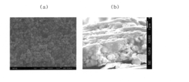
- the thin film of the thermoelectric conversion material obtained in Example 5 of this invention is shown, (a) is the SEM photograph (measurement magnification 3000 times) of the plane of a thin film, (b) is the SEM photograph (measurement magnification) of the cross section of a thin film. 8000 times).
- thermoelectric conversion material The thermoelectric conversion material of the present invention is characterized by having a thin film made of a thermoelectric semiconductor composition containing thermoelectric semiconductor fine particles and a conductive polymer on a support.
- the support used for the thermoelectric conversion material of the present invention is not particularly limited as long as it does not affect the decrease in electrical conductivity and the increase in thermal conductivity of the thermoelectric conversion material.
- Examples of the support include glass, silicon, and a plastic substrate.
- thermoelectric semiconductor materials telluride-based thermoelectric semiconductor materials such as GeTe and PbTe; antimony-tellurium-based thermoelectric semiconductor materials; zinc-antimony-based thermoelectric semiconductor materials such as ZnSb, Zn 3 Sb 2 and Zn 4 Sb 3 ; silicon such as SiGe Germanium-based thermoelectric semiconductor materials; Bismuth selenide-based thermoelectric semiconductor materials such as Bi 2 Se 3 ; Silicide-based thermoelectric semiconductor materials such as ⁇ -FeSi 2 , CrSi 2 , MnSi 1.73 and Mg 2 Si; Oxide-based thermoelectric semiconductor materials; A Heusler material such as FeVAlSi or FeVTiAl is used.
- thermoelectric semiconductor material used in the present invention is preferably a bismuth-tellurium-based thermoelectric semiconductor material such as p-type bismuth telluride, n-type bismuth telluride, or Bi 2 Te 3 .
- p-type bismuth telluride carriers are holes and the Seebeck coefficient is a positive value, and for example, those represented by Bi x Te 3 Sb 2 -x are preferably used.
- X is preferably 0 ⁇ X ⁇ 0.6, and more preferably 0.4 ⁇ X ⁇ 0.6.
- X is greater than 0 and less than or equal to 0.6 because the Seebeck coefficient and electrical conductivity are increased, and the characteristics as a p-type thermoelectric conversion material are maintained.
- the n-type bismuth telluride is preferably one in which the carrier is an electron and the Seebeck coefficient is a negative value, for example, Bi 2 Te 3 -Y Se Y.
- Y is preferably 0 ⁇ Y ⁇ 3, more preferably 0.1 ⁇ Y ⁇ 2.7. It is preferable that Y is greater than 0 and less than or equal to 3 because the Seebeck coefficient and electrical conductivity are increased, and the characteristics as an n-type thermoelectric conversion material are maintained.
- the amount of the thermoelectric semiconductor fine particles used in the present invention in the thermoelectric semiconductor composition is preferably 30 to 99% by mass. More preferably, it is 50 to 96% by mass, and particularly preferably 70 to 95% by mass. If the blending amount of the thermoelectric semiconductor fine particles is within the above range, the absolute value of the Seebeck coefficient is large, the decrease in electrical conductivity is suppressed, and only the thermal conductivity is reduced. A film having film strength and flexibility is preferably obtained.
- thermoelectric semiconductor fine particles was obtained by measuring with a laser diffraction particle size analyzer (CILAS, type 1064), and was the median value of the particle size distribution.
- the conductive polymer is not particularly limited as long as it has a film-forming property and exhibits conductivity.
- Polythiophenes are high molecular weight thiophenes, such as poly-3-methylthiophene, poly-3-ethylthiophene, poly-3-methoxythiophene, poly-3-ethoxythiophene, poly (3,4-ethylenedioxythiophene) ( And a polymer such as PEDOT).
- Examples of the derivatives of polythiophenes include those obtained by doping or mixing the above polythiophenes with a dopant.
- Polymer ions such as alkylbenzene sulfonate ion, alkyl sulfonate ion, polyacrylate ion, polyvinyl sulfonate ion, polystyrene sulfonate ion (PSS), poly (2-acrylamido-2-methylpropane sulfonate) ion
- PSS polystyrene sulfonate
- PEDOT poly(3,4-ethylenedioxythiophene)
- PSS polystyrene sulfonate ion
- Polyanilines are high molecular weight anilines such as poly-2-methylaniline, poly-3-methylaniline, poly-2-ethylaniline, poly-3-ethylaniline, poly-2-methoxyaniline, poly-3-methoxyaniline, Poly-2-ethoxyaniline, poly-3-ethoxyaniline, poly-N-methylaniline, poly-N-propylaniline, poly-N-phenyl-1-naphthylaniline, poly-8-anilino-1-naphthalenesulfonic acid, poly-2-aminobenzene Examples thereof include sulfonic acid and poly 7-anilino-4-hydroxy-2-naphthalene sulfonic acid.
- polyaniline derivatives examples include those obtained by doping or mixing the above-mentioned polyanilines with a dopant.
- a dopant the dopant illustrated by the thiophene derivative can be used. These may be used alone or in combination of two or more.
- polyacrylic acid ions, polyvinyl sulfonic acid ions, polystyrene sulfonic acid ions (PSS), poly (2-acrylamido-2-methylpropane sulfonic acid) ions, etc. can be obtained from the point that high conductivity can be obtained.
- Polymer ions are preferred, and polystyrene sulfonate ions (PSS), which are water-soluble and strongly acidic polymers, are more preferred.
- the conductive polymer is preferably at least one or a mixture of two or more selected from polythiophenes, polyanilines and polypyrroles, and derivatives thereof. Derivatives are particularly preferred.
- the blending amount of the conductive polymer in the thermoelectric semiconductor composition is preferably 1 to 70% by mass, more preferably 4 to 50% by mass, and particularly preferably 5 to 30% by mass. When the blending amount of the conductive polymer is within the above range, a film having both high thermoelectric performance and film strength can be obtained.
- thermoelectric semiconductor composition comprising the thermal semiconductor fine particles and the conductive polymer used in the present invention may further contain other components such as a polymer component other than the conductive polymer and an organic compound having a boiling point of 100 ° C. or higher. Good.
- vinyl alcohol copolymer such as vinyl alcohol / vinyl acetate copolymer
- polyvinyl pyridine polyvinyl pyrrolidone and the like.
- the blending amount of the polymer component in the thermoelectric semiconductor composition is preferably 0 to 40% by mass, more preferably 0 to 20% by mass, and particularly preferably 1 to 20% by mass. When the blending amount of the polymer component is within the above range, a film having both high thermoelectric performance and film strength can be obtained.
- the organic compound having a boiling point of 100 ° C. or higher is added for the purpose of improving the conductivity of the conductive polymer and improving the thermoelectric performance.
- the organic compound has a boiling point of 100 ° C. or higher, it is preferable that when used as a heat conversion material, it does not volatilize and scatter in the normal use environment and operating environment, and the effect of improving thermoelectric performance is obtained.
- examples of such organic compounds include polyhydric alcohols, water-soluble pyrrolidones, and hydrophilic aprotic compounds.
- water-soluble pyrrolidones examples include N-methylpyrrolidone, N-ethylpyrrolidone, N-propylpyrrolidone, N-isopropylpyrrolidone, N-butylpyrrolidone, Nt-butylpyrrolidone, N-pentylpyrrolidone, N-hexyl.
- Pyrrolidone N-heptylpyrrolidone, N-cyclohexylpyrrolidone, N-octylpyrrolidone, N- (2-ethylhexyl) pyrrolidone, N-phenylpyrrolidone, N-benzylpyrrolidone, phenethylpyrrolidone, 2-methoxyethylpyrrolidone, 2-methoxypropylpyrrolidone 2-hydroxypropylpyrrolidone, vinylpyrrolidone, 2-pyrrolidone and the like, and one or more of these may be used.
- examples of the hydrophilic aprotic compound include dimethyl sulfoxide (DMSO) and N, N-dimethylformamide (DMF).
- DMSO dimethyl sulfoxide
- DMF N, N-dimethylformamide
- the blending amount of the organic compound in the thermoelectric semiconductor composition is preferably 0 to 40% by mass, more preferably 1 to 20% by mass. When the blending amount of the organic compound is within the above range, a film having high thermoelectric performance can be obtained.
- thermoelectric semiconductor composition comprising the thermal semiconductor fine particles and the conductive polymer used in the present invention
- a dispersant if necessary, a film-forming aid, a light stabilizer, an antioxidant, a tackifier, a plasticizer,
- Other additives such as a colorant, a resin stabilizer, a filler, a pigment, and a conductive auxiliary agent may be included. These additives can be used alone or in combination of two or more.
- thermoelectric semiconductor composition used in the present invention is not particularly limited, and the thermoelectric semiconductor fine particles and the conductive high particles can be obtained by a known method such as an ultrasonic homogenizer, a spiral mixer, a planetary mixer, a disperser, or a hybrid mixer.
- the thermoelectric semiconductor composition may be prepared by adding molecules, other components and additives as required, and further adding a solvent and mixing and dispersing them.
- the solvent include water, toluene, ethyl acetate, methyl ethyl ketone, alcohol, tetrahydrofuran, and the like. These solvents may be used alone or in a combination of two or more.
- the solid content concentration of the thermoelectric semiconductor composition is not particularly limited as long as the composition has a viscosity suitable for coating.
- the thin film comprising the thermoelectric semiconductor composition can be formed by applying the thermoelectric semiconductor composition on a support and drying, as will be described in the method for producing a thermoelectric conversion material of the present invention described later. .
- a large-area thermoelectric conversion material can be obtained easily at low cost.
- thermoelectric conversion material of the present invention can be used alone, for example, a plurality are electrically connected in series via electrodes, and thermally connected in parallel via an insulator such as ceramics,
- the thermoelectric conversion element can be used for power generation and cooling.
- the thermoelectric semiconductor fine particles have been annealed.
- the thermoelectric semiconductor fine particles can be annealed in advance before preparing the thermoelectric semiconductor composition.
- the annealing treatment is usually performed in a temperature range below the melting point of the thermoelectric semiconductor fine particles. More specifically, the annealing treatment temperature is preferably in the temperature range below the melting point of the thermoelectric semiconductor fine particles and at least 20% of the melting point.
- the support used in the present invention is as described above, and is glass, silicon, plastic or the like.
- a method for applying the thermoelectric semiconductor composition of the present invention on a support known methods such as screen printing, flexographic printing, gravure printing, spin coating, dip coating, die coating, spray coating, bar coating, doctor blade, and the like are available. There are no particular restrictions.
- screen printing, die coating or the like is preferably used.
- a thin film is formed by drying the obtained coating film.
- conventionally known drying methods such as hot air drying, hot roll drying, and infrared irradiation can be adopted.
- the heating temperature is usually from 80 to 150 ° C., and the heating time is usually from several tens of seconds to several tens of minutes, depending on the heating method.
- the heating temperature is not particularly limited as long as the used solvent can be dried, but does not adversely affect other substances constituting the composition. It is preferable to set the temperature range.
- the obtained thermoelectric conversion material may be further subjected to annealing treatment after the thin film is formed. By performing the annealing treatment, the thermoelectric performance can be stabilized and further improved.
- thermoelectromotive force was measured from the electrode adjacent to the thermocouple installation position.
- the distance between both ends of the sample for measuring the temperature difference and the electromotive force is 25 mm, one end is kept at 20 ° C., and the other end is heated from 25 ° C. to 50 ° C. in 1 ° C. increments.
- the electric power was measured, and the Seebeck coefficient (S) was calculated from the slope.
- the installation position of the thermocouple and the electrode is symmetrical with respect to the center line of the thin film, and the distance between the thermocouple and the electrode is 1 mm.
- the average particle size of the fine particles of the obtained bismuth-tellurium-based thermoelectric semiconductor material was 660 nm (T1), 2.8 ⁇ m (T2), 5.5 ⁇ m (T3), and 180 ⁇ m (T4), respectively.
- (Bismuth selenide-based thermoelectric semiconductor material) Bi 2 Se 3 manufactured by High-Purity Chemical Laboratory, particle size: 80 ⁇ m
- T5 and T6 thermoelectric semiconductor fine particles
- the average particle sizes of the obtained bismuth selenide thermoelectric semiconductor materials were 0.88 ⁇ m (T5) and 20 ⁇ m (T6), respectively.
- thermoelectric semiconductor fine particles (T1) were annealed twice in total under the same conditions as (1) to obtain p-type bismuth telluride fine particles (S2).
- the average particle diameter of the annealed thermoelectric semiconductor fine particles (S2) was 5 ⁇ m.
- a thermoelectric conversion material was produced in the same manner as in Example 1 except that the annealed thermoelectric semiconductor fine particles (S2) were used instead of S1.
- thermoelectric conversion material was produced in the same manner as in Example 1 except that T1 was used as it was without annealing the thermoelectric semiconductor fine particles (T1).
- FIG. 2 shows a thin film made of the thermoelectric semiconductor composition obtained in Example 5, wherein (a) is a planar SEM photograph and (b) is a cross-sectional SEM photograph.
- thermoelectric conversion material was produced in the same manner as in Example 5 except that the blending amount of the thermoelectric semiconductor fine particles was 80% by mass, and the blending amounts of PEDOT: PSS, glycerin, and acrylic acid polymer were as shown in Table 1.
- thermoelectric conversion material was produced in the same manner as in Example 5 except that the thermoelectric semiconductor fine particles were changed from T1 to T2.
- thermoelectric conversion material was produced in the same manner as in Example 7 except that the blending amount of the thermoelectric semiconductor fine particles was 80% by mass and the blending amounts of PEDOT: PSS, glycerin, and acrylic acid polymer were the blending amounts shown in Table 1.
- Example 9 A thermoelectric conversion material was produced in the same manner as in Example 5 except that the thermoelectric semiconductor fine particles were changed from T1 to T3.
- thermoelectric conversion material was prepared in the same manner as in Example 9 except that the blending amount of the thermoelectric semiconductor fine particles was 80% by mass and the blending amounts of PEDOT: PSS, glycerin, and acrylic acid polymer were those shown in Table 1.
- thermoelectric conversion material was produced in the same manner as in Example 5 except that PEDOT: PSS was blended in the amounts shown in Table 1 and glycerin and an acrylic acid polymer were not blended.
- thermoelectric conversion material was produced in the same manner as in Example 11 except that the blending amount of the thermoelectric semiconductor fine particles was 80% by mass and PEDOT: PSS was the blending amount shown in Table 1.
- thermoelectric conversion material was produced in the same manner as in Example 11 except that the blending amount of the thermoelectric semiconductor fine particles was 60% by mass and PEDOT: PSS was the blending amount shown in Table 1.
- thermoelectric conversion material was prepared in the same manner as in Example 11 except that the blending amount of the thermoelectric semiconductor fine particles was 40 mass% and PEDOT: PSS was the blending amount shown in Table 1.
- thermoelectric conversion material was produced in the same manner as in Example 11 except that the thermoelectric semiconductor fine particles were changed from T1 to T2.
- thermoelectric conversion material was produced in the same manner as in Example 11 except that the thermoelectric semiconductor fine particles were changed from T1 to T3.
- thermoelectric conversion material was produced in the same manner as in Example 17 except that the blending amount of the thermoelectric semiconductor fine particles was 80% by mass and PEDOT: PSS was the blending amount shown in Table 1.
- thermoelectric conversion material was produced in the same manner as in Example 5 except that the thermoelectric semiconductor fine particles were changed from T1 to T4.
- thermoelectric conversion material was produced in the same manner as in Example 5 except that the thermoelectric semiconductor fine particles were changed from T1 to fine particles T6 of a bismuth selenide thermoelectric semiconductor material.
- thermoelectric semiconductor composition only PEDOT: PSS, which is a conductive polymer, was used, and a thin film having a thickness of 100 nm was formed in the same manner as in Example 1 to produce a thermoelectric conversion material.
- thermoelectric semiconductor composition PEDOT: PSS, glycerin, and an acrylic acid polymer were blended in amounts shown in Table 1 to prepare a coating liquid made of the thermoelectric semiconductor composition. Using this coating liquid, a thin film having a thickness of 5000 nm was formed in the same manner as in Example 1 to produce a thermoelectric conversion material.
- thermoelectric performance evaluation results of the thermoelectric conversion materials obtained in Examples 1 to 20 and Comparative Examples 1 and 2 are shown in Table 1.
- thermoelectric conversion material was produced in the same manner as in Example 5 except that the support was replaced with a glass substrate and a polyethylene terephthalate film (product name: Cosmo Shine PET100A4100, hereinafter referred to as PET substrate) was used.
- PET substrate polyethylene terephthalate film
- thermoelectric conversion material was produced in the same manner as in Example 7 except that the glass substrate was replaced with a PET substrate.
- thermoelectric semiconductor composition As a thermoelectric semiconductor composition, only thermoelectric semiconductor fine particles (T1) are dispersed in an ethanol solvent, sprayed onto a PET substrate by spray coating, dried at 110 ° C. for 10 minutes in an argon atmosphere, and a thin film having a thickness of 1000 nm (Pellet-shaped thermoelectric semiconductor composition) was produced.
- thermoelectric conversion materials obtained in Examples 21 to 23 and Comparative Example 3 show the flexibility evaluation results regarding the thermoelectric conversion materials obtained in Examples 21 to 23 and Comparative Example 3. It was found that the thermoelectric conversion materials of Examples 21 to 23 including the thermoelectric semiconductor fine particles and the conductive polymer were excellent in flexibility with almost no decrease in the dimensionless thermoelectric figure of merit ZT before and after the cylindrical mandrel test. . On the other hand, in the thermoelectric conversion material of Comparative Example 3 composed only of thermoelectric semiconductor fine particles, the flexibility was low, and the thin film after the cylindrical mandrel test could not maintain the shape, and thus did not function as the thermoelectric conversion material.
- thermoelectric conversion material of the present invention is used as a thermoelectric conversion element that performs mutual energy conversion between heat and electricity and is incorporated into a module. Specifically, a thermoelectric conversion material that can be easily manufactured at low cost and has excellent thermoelectric performance is obtained. For example, when installing on a wall surface of a building, a low-cost thermoelectric conversion material is used for a large area. Can be used as
Priority Applications (5)
| Application Number | Priority Date | Filing Date | Title |
|---|---|---|---|
| CN201380015224.3A CN104205383B (zh) | 2012-03-21 | 2013-03-11 | 热电转换材料及其制造方法 |
| EP13765181.6A EP2830106B1 (en) | 2012-03-21 | 2013-03-11 | Thermoelectric conversion material and method for manufacturing same |
| KR1020147025805A KR102065327B1 (ko) | 2012-03-21 | 2013-03-11 | 열전 변환 재료 및 그 제조 방법 |
| US14/385,595 US9461228B2 (en) | 2012-03-21 | 2013-03-11 | Thermoelectric conversion material and method for manufacturing same |
| JP2014506146A JP6127041B2 (ja) | 2012-03-21 | 2013-03-11 | 熱電変換材料及びその製造方法 |
Applications Claiming Priority (2)
| Application Number | Priority Date | Filing Date | Title |
|---|---|---|---|
| JP2012064245 | 2012-03-21 | ||
| JP2012-064245 | 2012-03-21 |
Publications (1)
| Publication Number | Publication Date |
|---|---|
| WO2013141065A1 true WO2013141065A1 (ja) | 2013-09-26 |
Family
ID=49222525
Family Applications (1)
| Application Number | Title | Priority Date | Filing Date |
|---|---|---|---|
| PCT/JP2013/056691 WO2013141065A1 (ja) | 2012-03-21 | 2013-03-11 | 熱電変換材料及びその製造方法 |
Country Status (7)
| Country | Link |
|---|---|
| US (1) | US9461228B2 (zh) |
| EP (1) | EP2830106B1 (zh) |
| JP (1) | JP6127041B2 (zh) |
| KR (1) | KR102065327B1 (zh) |
| CN (1) | CN104205383B (zh) |
| TW (1) | TWI618271B (zh) |
| WO (1) | WO2013141065A1 (zh) |
Cited By (10)
| Publication number | Priority date | Publication date | Assignee | Title |
|---|---|---|---|---|
| JP2015115447A (ja) * | 2013-12-11 | 2015-06-22 | 高圧ガス工業株式会社 | 発電デバイス |
| JP2015162502A (ja) * | 2014-02-26 | 2015-09-07 | トヨタ紡織株式会社 | 有機無機ハイブリッド膜の製造方法、有機無機ハイブリッド膜 |
| JP2016001711A (ja) * | 2014-06-12 | 2016-01-07 | 日本電信電話株式会社 | 熱電変換材料およびその製造方法 |
| JP2016063177A (ja) * | 2014-09-22 | 2016-04-25 | トヨタ紡織株式会社 | 複合膜、及びその製造方法 |
| JP2016163039A (ja) * | 2015-02-27 | 2016-09-05 | コリア・ユニバーシティ・リサーチ・アンド・ビジネス・ファウンデーション | フレキシブル熱電発電モジュール及びその製造方法 |
| JP2016539887A (ja) * | 2013-09-27 | 2016-12-22 | エルジー・ケム・リミテッド | 新規な化合物半導体及びその活用 |
| WO2018110403A1 (ja) * | 2016-12-13 | 2018-06-21 | リンテック株式会社 | 熱電変換材料及びその製造方法 |
| JP2020123744A (ja) * | 2015-01-05 | 2020-08-13 | ザ・ボーイング・カンパニーThe Boeing Company | 熱電発電機 |
| WO2023013590A1 (ja) * | 2021-08-02 | 2023-02-09 | リンテック株式会社 | 熱電変換材料層及び熱電変換モジュール |
| JP7386801B2 (ja) | 2018-10-03 | 2023-11-27 | リンテック株式会社 | 熱電変換モジュール用中間体の製造方法 |
Families Citing this family (12)
| Publication number | Priority date | Publication date | Assignee | Title |
|---|---|---|---|---|
| CN105051925B (zh) * | 2013-03-27 | 2018-07-17 | 株式会社日立制作所 | 高效率热电转换装置 |
| FR3009133B1 (fr) * | 2013-07-24 | 2016-10-28 | Commissariat Energie Atomique | Procede de fabrication d'un module thermoelectrique a base de film polymere |
| CN104641479B (zh) | 2013-08-09 | 2016-06-15 | 琳得科株式会社 | 热电转换材料及其制造方法 |
| CN104436567A (zh) * | 2013-09-25 | 2015-03-25 | 高尔夫泰克有限责任公司 | 高尔夫球压缩设备 |
| WO2016164695A1 (en) * | 2015-04-09 | 2016-10-13 | Nitto Denko Corporation | Thermoelectric component and method of making same |
| WO2018056368A1 (ja) * | 2016-09-21 | 2018-03-29 | 日産化学工業株式会社 | 熱電変換層形成用組成物及び熱電変換層の製造方法 |
| TWI608639B (zh) | 2016-12-06 | 2017-12-11 | 財團法人工業技術研究院 | 可撓熱電結構與其形成方法 |
| CN109411593B (zh) * | 2018-10-31 | 2022-09-20 | 北京航空航天大学杭州创新研究院 | 一种n型聚苯胺基热电复合膜的制备方法 |
| CN110433512A (zh) * | 2019-08-28 | 2019-11-12 | 农业农村部南京农业机械化研究所 | 一种水浴式折射窗浆液干燥设备 |
| US11611029B2 (en) * | 2020-05-21 | 2023-03-21 | Saudi Arabian Oil Company | Methods to harvest thermal energy during subsurface high power laser transmission |
| CN114226210A (zh) * | 2021-12-16 | 2022-03-25 | 华东师范大学 | 一种硒化银热电复合薄膜及其制备方法和应用 |
| CN115385307A (zh) * | 2022-07-15 | 2022-11-25 | 浙江先导热电科技股份有限公司 | 一种碲化铋微纳米粉体材料的制备方法及应用 |
Citations (4)
| Publication number | Priority date | Publication date | Assignee | Title |
|---|---|---|---|---|
| JP2003046145A (ja) * | 2001-04-27 | 2003-02-14 | Naoki Toshima | 熱電材料及び熱電素子並びに熱電材料の製造方法 |
| JP2006040963A (ja) * | 2004-07-22 | 2006-02-09 | Yamaha Corp | 熱電モジュールの製造方法 |
| JP2010199276A (ja) | 2009-02-25 | 2010-09-09 | Konica Minolta Holdings Inc | 熱電変換素子およびその製造方法 |
| JP2012009462A (ja) * | 2009-09-14 | 2012-01-12 | Tokyo Univ Of Science | 有機−無機ハイブリッド熱電材料、当該熱電材料を用いた熱電変換素子及び有機−無機ハイブリッド熱電材料の製造方法 |
Family Cites Families (8)
| Publication number | Priority date | Publication date | Assignee | Title |
|---|---|---|---|---|
| US6759587B2 (en) * | 2001-04-27 | 2004-07-06 | Hokushin Corporation | Thermoelectric materials, thermoelectric device, and method for producing thermoelectric materials |
| WO2004049464A1 (ja) * | 2002-11-28 | 2004-06-10 | Sumitomo Electric Industries, Ltd. | 熱電材料及びその製造方法 |
| JP4296784B2 (ja) * | 2003-01-16 | 2009-07-15 | パナソニック電工株式会社 | 熱電変換材料の製造方法 |
| JP4876501B2 (ja) * | 2005-09-22 | 2012-02-15 | 宇部興産株式会社 | 熱電変換材料及びその製造方法 |
| US8044292B2 (en) * | 2006-10-13 | 2011-10-25 | Toyota Motor Engineering & Manufacturing North America, Inc. | Homogeneous thermoelectric nanocomposite using core-shell nanoparticles |
| JP5243181B2 (ja) * | 2008-10-20 | 2013-07-24 | スリーエム イノベイティブ プロパティズ カンパニー | 導電性高分子複合体及び導電性高分子材料を用いた熱電素子 |
| CN101931043B (zh) * | 2009-06-19 | 2013-03-20 | 清华大学 | 热电转换材料 |
| TW201131582A (en) * | 2009-12-25 | 2011-09-16 | Fujifilm Corp | Conductive film, method for producing the same, and touch panel |
-
2013
- 2013-03-11 EP EP13765181.6A patent/EP2830106B1/en not_active Not-in-force
- 2013-03-11 KR KR1020147025805A patent/KR102065327B1/ko active IP Right Grant
- 2013-03-11 CN CN201380015224.3A patent/CN104205383B/zh not_active Expired - Fee Related
- 2013-03-11 WO PCT/JP2013/056691 patent/WO2013141065A1/ja active Application Filing
- 2013-03-11 JP JP2014506146A patent/JP6127041B2/ja not_active Expired - Fee Related
- 2013-03-11 US US14/385,595 patent/US9461228B2/en active Active
- 2013-03-19 TW TW102109637A patent/TWI618271B/zh not_active IP Right Cessation
Patent Citations (4)
| Publication number | Priority date | Publication date | Assignee | Title |
|---|---|---|---|---|
| JP2003046145A (ja) * | 2001-04-27 | 2003-02-14 | Naoki Toshima | 熱電材料及び熱電素子並びに熱電材料の製造方法 |
| JP2006040963A (ja) * | 2004-07-22 | 2006-02-09 | Yamaha Corp | 熱電モジュールの製造方法 |
| JP2010199276A (ja) | 2009-02-25 | 2010-09-09 | Konica Minolta Holdings Inc | 熱電変換素子およびその製造方法 |
| JP2012009462A (ja) * | 2009-09-14 | 2012-01-12 | Tokyo Univ Of Science | 有機−無機ハイブリッド熱電材料、当該熱電材料を用いた熱電変換素子及び有機−無機ハイブリッド熱電材料の製造方法 |
Non-Patent Citations (2)
| Title |
|---|
| D. MADAN, JOURNAL OF APPLIED PHYSICS, vol. 109, 2011, pages 034904 |
| See also references of EP2830106A4 |
Cited By (13)
| Publication number | Priority date | Publication date | Assignee | Title |
|---|---|---|---|---|
| JP2016539887A (ja) * | 2013-09-27 | 2016-12-22 | エルジー・ケム・リミテッド | 新規な化合物半導体及びその活用 |
| JP2015115447A (ja) * | 2013-12-11 | 2015-06-22 | 高圧ガス工業株式会社 | 発電デバイス |
| JP2015162502A (ja) * | 2014-02-26 | 2015-09-07 | トヨタ紡織株式会社 | 有機無機ハイブリッド膜の製造方法、有機無機ハイブリッド膜 |
| JP2016001711A (ja) * | 2014-06-12 | 2016-01-07 | 日本電信電話株式会社 | 熱電変換材料およびその製造方法 |
| JP2016063177A (ja) * | 2014-09-22 | 2016-04-25 | トヨタ紡織株式会社 | 複合膜、及びその製造方法 |
| JP2020123744A (ja) * | 2015-01-05 | 2020-08-13 | ザ・ボーイング・カンパニーThe Boeing Company | 熱電発電機 |
| JP2016163039A (ja) * | 2015-02-27 | 2016-09-05 | コリア・ユニバーシティ・リサーチ・アンド・ビジネス・ファウンデーション | フレキシブル熱電発電モジュール及びその製造方法 |
| WO2018110403A1 (ja) * | 2016-12-13 | 2018-06-21 | リンテック株式会社 | 熱電変換材料及びその製造方法 |
| JPWO2018110403A1 (ja) * | 2016-12-13 | 2019-10-24 | リンテック株式会社 | 熱電変換材料及びその製造方法 |
| JP7173869B2 (ja) | 2016-12-13 | 2022-11-16 | リンテック株式会社 | 熱電変換材料及びその製造方法 |
| US11522114B2 (en) | 2016-12-13 | 2022-12-06 | Lintec Corporation | Thermoelectric conversion material and method for producing same |
| JP7386801B2 (ja) | 2018-10-03 | 2023-11-27 | リンテック株式会社 | 熱電変換モジュール用中間体の製造方法 |
| WO2023013590A1 (ja) * | 2021-08-02 | 2023-02-09 | リンテック株式会社 | 熱電変換材料層及び熱電変換モジュール |
Also Published As
| Publication number | Publication date |
|---|---|
| US9461228B2 (en) | 2016-10-04 |
| KR20140138166A (ko) | 2014-12-03 |
| KR102065327B1 (ko) | 2020-01-13 |
| TW201347249A (zh) | 2013-11-16 |
| EP2830106A4 (en) | 2015-11-18 |
| EP2830106A1 (en) | 2015-01-28 |
| CN104205383A (zh) | 2014-12-10 |
| CN104205383B (zh) | 2017-05-17 |
| TWI618271B (zh) | 2018-03-11 |
| JP6127041B2 (ja) | 2017-05-10 |
| US20150048283A1 (en) | 2015-02-19 |
| EP2830106B1 (en) | 2018-05-02 |
| JPWO2013141065A1 (ja) | 2015-08-03 |
Similar Documents
| Publication | Publication Date | Title |
|---|---|---|
| JP6127041B2 (ja) | 熱電変換材料及びその製造方法 | |
| Lindorf et al. | Organic-based thermoelectrics | |
| EP2884550B1 (en) | Thermoelectric conversion material and production method therefor | |
| Nandihalli et al. | Polymer based thermoelectric nanocomposite materials and devices: Fabrication and characteristics | |
| Yue et al. | Poly (3, 4-ethylenedioxythiophene) as promising organic thermoelectric materials: A mini-review | |
| JP6683132B2 (ja) | ペルチェ冷却素子及びその製造方法 | |
| US11522114B2 (en) | Thermoelectric conversion material and method for producing same | |
| JP5599095B2 (ja) | 有機−無機ハイブリッド熱電材料の製造方法 | |
| KR102170477B1 (ko) | 열전소자용 페이스트 조성물, 이를 이용한 열전소자의 제조방법, 및 열전소자 | |
| Mardi et al. | Developing printable thermoelectric materials based on graphene nanoplatelet/ethyl cellulose nanocomposites | |
| Abd Rahman et al. | Effect of bismuth telluride concentration on the thermoelectric properties of PEDOT: PSS–glycerol organic films | |
| Culebras et al. | Hybrids composites of NCCO/PEDOT for thermoelectric applications | |
| Kang et al. | Experimental investigation of the dependence of the thermoelectric performance of carbon nanotubes/polymer nanocomposites on the synthesis protocol | |
| Nayak et al. | Effect of graphite on the power density of selenium doped polyaniline ink based hybrid screen-printed flexible thermoelectric generator | |
| EP4089749A1 (en) | Ink composition for printable thermoelectric materials | |
| Maity et al. | Polymer chalcogenides—new smart materials for thermoelectric applications | |
| JP6791544B2 (ja) | 熱電半導体組成物、並びに熱電変換材料及びその製造方法 |
Legal Events
| Date | Code | Title | Description |
|---|---|---|---|
| 121 | Ep: the epo has been informed by wipo that ep was designated in this application |
Ref document number: 13765181 Country of ref document: EP Kind code of ref document: A1 |
|
| ENP | Entry into the national phase |
Ref document number: 2014506146 Country of ref document: JP Kind code of ref document: A |
|
| ENP | Entry into the national phase |
Ref document number: 20147025805 Country of ref document: KR Kind code of ref document: A |
|
| WWE | Wipo information: entry into national phase |
Ref document number: 14385595 Country of ref document: US Ref document number: 2013765181 Country of ref document: EP |
|
| NENP | Non-entry into the national phase |
Ref country code: DE |