WO2013118214A1 - Dispositif d'affichage d'informations - Google Patents
Dispositif d'affichage d'informations Download PDFInfo
- Publication number
- WO2013118214A1 WO2013118214A1 PCT/JP2012/007520 JP2012007520W WO2013118214A1 WO 2013118214 A1 WO2013118214 A1 WO 2013118214A1 JP 2012007520 W JP2012007520 W JP 2012007520W WO 2013118214 A1 WO2013118214 A1 WO 2013118214A1
- Authority
- WO
- WIPO (PCT)
- Prior art keywords
- coordinate detection
- light
- detection mark
- display device
- electronic pen
- Prior art date
Links
Images


Classifications
-
- G—PHYSICS
- G06—COMPUTING; CALCULATING OR COUNTING
- G06F—ELECTRIC DIGITAL DATA PROCESSING
- G06F3/00—Input arrangements for transferring data to be processed into a form capable of being handled by the computer; Output arrangements for transferring data from processing unit to output unit, e.g. interface arrangements
- G06F3/01—Input arrangements or combined input and output arrangements for interaction between user and computer
- G06F3/03—Arrangements for converting the position or the displacement of a member into a coded form
- G06F3/033—Pointing devices displaced or positioned by the user, e.g. mice, trackballs, pens or joysticks; Accessories therefor
- G06F3/0354—Pointing devices displaced or positioned by the user, e.g. mice, trackballs, pens or joysticks; Accessories therefor with detection of 2D relative movements between the device, or an operating part thereof, and a plane or surface, e.g. 2D mice, trackballs, pens or pucks
- G06F3/03545—Pens or stylus
-
- G—PHYSICS
- G06—COMPUTING; CALCULATING OR COUNTING
- G06F—ELECTRIC DIGITAL DATA PROCESSING
- G06F3/00—Input arrangements for transferring data to be processed into a form capable of being handled by the computer; Output arrangements for transferring data from processing unit to output unit, e.g. interface arrangements
- G06F3/01—Input arrangements or combined input and output arrangements for interaction between user and computer
- G06F3/03—Arrangements for converting the position or the displacement of a member into a coded form
- G06F3/0304—Detection arrangements using opto-electronic means
- G06F3/0317—Detection arrangements using opto-electronic means in co-operation with a patterned surface, e.g. absolute position or relative movement detection for an optical mouse or pen positioned with respect to a coded surface
- G06F3/0321—Detection arrangements using opto-electronic means in co-operation with a patterned surface, e.g. absolute position or relative movement detection for an optical mouse or pen positioned with respect to a coded surface by optically sensing the absolute position with respect to a regularly patterned surface forming a passive digitiser, e.g. pen optically detecting position indicative tags printed on a paper sheet
-
- H—ELECTRICITY
- H10—SEMICONDUCTOR DEVICES; ELECTRIC SOLID-STATE DEVICES NOT OTHERWISE PROVIDED FOR
- H10K—ORGANIC ELECTRIC SOLID-STATE DEVICES
- H10K59/00—Integrated devices, or assemblies of multiple devices, comprising at least one organic light-emitting element covered by group H10K50/00
- H10K59/40—OLEDs integrated with touch screens
Definitions
- a coordinate detection marker is formed in a display area in a display device such as an EL display device in which electroluminescence (hereinafter referred to as EL) elements using an organic material as a light emitting material are arranged in a matrix, and this coordinate detection is performed.
- EL electroluminescence
- the present invention relates to an information display device that reads a marker with an input pen or the like.
- a technique is known in which a position of image information formed on a print medium is specified by placing a two-dimensional code including encoded coordinate information on a print medium such as paper.
- a technique for inputting coordinates there is a technique of inputting coordinates on a tablet with a stylus pen as an input pen by a method such as a resistance pressure type, a capacitance type or an electromagnetic induction type.
- a method such as a resistance pressure type, a capacitance type or an electromagnetic induction type.
- a tablet and a display means such as a liquid crystal display are often used in combination.
- Patent Documents 1 and 2 are known.
- JP 2006-085679 A Japanese Patent Application Laid-Open No. 07-17304
- the present disclosure is an information display device having a display panel including a display area in which pixels are arranged in a matrix.
- the display panel includes a polarization unit that polarizes incident light, and a coordinate detection mark provided so as to change the polarization state of the polarization unit.
- the coordinate position can be easily specified by detecting the light passing through the coordinate detection mark or the reflected light with the image acquisition means.
- FIG. 1 is a configuration diagram illustrating a schematic configuration of a pixel and an example of a driving circuit of an EL display device according to an embodiment.
- FIG. 2A is an explanatory diagram of an initial operation of a pixel of an EL display device according to an embodiment.
- FIG. 2B is an explanatory diagram of a pixel reset operation of the EL display device according to the embodiment.
- FIG. 2C is an explanatory diagram of a pixel program operation of the EL display device according to the embodiment.
- FIG. 2D is an explanatory diagram of the light emission operation of the pixel of the EL display device according to one embodiment.
- FIG. 3 is a cross-sectional view illustrating an example of an EL display panel of an EL display device according to an embodiment.
- FIG. 4 is a cross-sectional view illustrating another example of the EL display panel of the EL display device according to the embodiment.
- FIG. 5 is an explanatory diagram illustrating an example of an information display device using the EL display device according to the embodiment.
- FIG. 6 is an explanatory diagram illustrating an example of an information display device using an EL display device according to an embodiment.
- FIG. 7 is a schematic diagram showing the basic configuration of an electronic pen and a tablet terminal in one embodiment.
- FIG. 8 is an explanatory diagram for explaining an example of reading information.
- FIG. 9 is an explanatory diagram of input by the electronic pen.
- FIG. 10 is an explanatory diagram of the LED and CCD control method.
- FIG. 11 is an explanatory diagram illustrating another example of an information display device using an EL display device according to an embodiment.
- FIG. 12 is an explanatory view showing a state where the LED is attached to the substrate and the state of LED lighting control.
- FIG. 13 is an explanatory diagram showing another example of a state where the LED is attached to the substrate or the like and a state where the lighting of the LED is controlled.
- FIG. 14 is an explanatory diagram showing another example of an information display device using an EL display device according to an embodiment.
- FIG. 15 is an explanatory diagram showing another example of an information display device using an EL display device according to an embodiment.
- FIG. 16 is an explanatory diagram illustrating another example of the information display device using the EL display device according to the embodiment.
- FIG. 17 is a diagram illustrating an arrangement example of coordinate detection marks.
- FIG. 18 is a diagram illustrating an arrangement example of coordinate detection marks.
- FIG. 19 is a diagram showing an example of arrangement of coordinate detection marks.
- FIG. 20 is a diagram illustrating an arrangement example of coordinate detection marks.
- FIG. 21 is a diagram showing an example of arrangement of coordinate detection marks.
- FIG. 22 is a diagram showing an example of arrangement of coordinate detection marks.
- FIG. 23 is a diagram showing an example of arrangement of coordinate detection marks.
- FIG. 24 is a diagram illustrating an arrangement example of coordinate detection marks.
- FIG. 25 is a diagram showing an example of arrangement of coordinate detection marks.
- FIG. 26 is a diagram showing an example of arrangement of coordinate detection marks.
- FIG. 27 is an explanatory diagram showing another example of an information display device using an EL display device according to an embodiment.
- FIG. 1 is a configuration diagram illustrating a schematic configuration of a pixel and an example of a driving circuit of an EL display device according to an embodiment. In FIG. 1, only the main part of the EL display device is shown.
- the EL display device includes an EL display panel 1 and a wiring board on which a drive circuit is mounted.
- the EL display panel 1 has a configuration in which a plurality of pixels having EL elements in the display region 2 are arranged in a matrix.
- One pixel 10 has a configuration in which the source terminal of the switching transistor 11d is connected to the drain terminal of the P-channel driving transistor 11a, and the anode terminal of the EL element 12 is connected to the drain terminal of the transistor 11d.
- Transistors 11b, 11c, 11e, and 11f are other switching transistors provided in the pixel 10
- capacitors 13a, 13b, 13c, 13d, and 13e are capacitors for controlling on / off of the transistors 11a to 11f. It is.
- the cathode voltage Vss is applied to the cathode terminal of the EL element 12, and the anode voltage Vdd is applied to the source terminal of the transistor 11a from the anode electrode of the EL display device.
- the cathode voltage Vss is set such that the anode voltage Vdd> the cathode voltage Vss.
- the drive circuit has a source driver IC 14 as a source driver circuit and gate driver ICs 15 and 16 as gate driver circuits.
- the source driver IC 14 and the gate driver ICs 15 and 16 and the pixel 10 are electrically connected via a gate signal line 17 (17a, 17b, 17c, 17d, and 17e) and a source signal line 18.
- the gate driver IC 15 is mounted on a flexible substrate (COF) 19 as a wiring substrate, and the gate driver IC 16 is connected to the EL display panel 1 through the COF 19.
- COF flexible substrate
- the source terminal and the drain terminal of the transistor 11b are connected between the gate terminal and the drain terminal of the transistor 11a, and the ON voltage is applied to the gate signal line 17b (Gb), whereby the gate terminal and the drain of the transistor 11a are applied.
- Gb gate signal line
- One terminal of the capacitor 13b is connected to the gate terminal of the transistor 11a, and the other terminal of the capacitor 13b is connected to the drain terminal of the transistor 11b.
- the source terminal of the transistor 11c is connected to the source signal line 18 through the transistor 11b.
- the on voltage of the gate signal line 17c (Gc) is applied to the gate terminal of the transistor 11c, the transistor 11c is turned on.
- the voltage Vs is applied to the pixel 10 in accordance with the video signal supplied to the source signal line 18.
- one terminal of the capacitor 13a of the pixel 10 is connected to the drain terminal of the transistor 11b, the other terminal is connected to the anode electrode of the EL display device, and the anode voltage Vdd is applied.
- the drain terminal of the transistor 11e is connected to the drain terminal of the transistor 11b, and the source terminal of the transistor 11e is connected to the signal line to which the reset voltage Va is applied.
- the transistor 11e is turned on, and the reset voltage Va is applied to the capacitor 13a.
- the transistors 11c and 11e are P-channel and adopt an LDD structure. That is, by adopting a structure in which the gates of a plurality of transistors are connected in series, the off characteristics of the transistors 11c and 11e can be improved. Transistors other than the transistors 11c and 11e also adopt a P-channel and preferably adopt an LDD structure. If necessary, a multi-gate structure can suppress off-leakage and realize a good contrast and offset canceling operation. it can.
- the transistor 11a may be configured to apply an arbitrary DC voltage other than the anode voltage Vdd.
- different voltages may be applied to the capacitor 13a and the source terminal of the transistor 11a instead of applying the same voltage.
- the anode terminal Vdd may be applied to the source terminal of the transistor 11a
- the DC voltage Vb (5 (V)) may be applied to the capacitor 13a.
- a predetermined voltage value is applied to the pixel 10 through the transistor 11b and corresponds to the gradation of the video signal.
- the transistor 11d is turned on and off, and gradation display is performed to perform light emission drive control. Further, the transistor 11d is turned on / off to generate a strip-shaped black display (non-display) in the display area 2 and to control the amount of current flowing through the display area 2.
- the capacitor 13c is formed between the gate signal line 17b and the transistor 11a
- the capacitor 13d is formed between the gate signal line 17d and the gate terminal of the transistor 11a.
- These capacitors 13c, 13d, etc. are called punch-through capacitors, and the voltage to be changed or the changed voltage is called a punch-through voltage.
- the transistor 11d when the transistor 11d is on, the VGL2 voltage is applied to the gate signal line 17d, and when the transistor 11d is off, the VGH2 voltage is applied to the gate signal line 17d.
- the transistor 11d is in an off state during the offset cancel operation, and is in an on state when the EL element 12 emits light. Therefore, at the start of display, the gate signal line 17d changes from the VGH2 voltage to the VGL2 voltage. Therefore, the voltage at the gate terminal of the transistor 11a is lowered by the action of the punch-through capacitor 13d.
- the transistor 11a When the voltage at the gate terminal of the transistor 11a decreases, the transistor 11a can pass a large current through the EL element 12, and high-luminance display is possible.
- the amplitude of the current flowing through the EL element 12 is increased, thereby enabling high luminance display.
- the capacity of the capacitor 13c is preferably 1/12 or more and 1/3 or less of the capacity of the capacitor 13a or 13b. If the capacitance ratio of the capacitor 13c is too small, the change rate of the gate terminal voltage of the transistor 11a becomes too large, and the difference from the ideal value in the offset canceled state becomes too large. On the other hand, if the capacitance ratio is too large, the change in the gate terminal voltage of the transistor 11a becomes small, and it is difficult to obtain the effect.
- the method of changing the gate terminal voltage of the driving transistor 11a is not limited to changing the voltage directly by the capacitor 13c.
- the gate terminal voltage of the driving transistor 11a may be indirectly changed through another capacitor.
- FIGS. 2A to 2D are explanatory diagrams of the operation of the pixel of the EL display device according to the embodiment.
- the lighting operation of the pixel 10 will be described in more detail with reference to FIGS. 2A to 2D.
- the operation of writing a video signal to the pixel and the light emitting operation of the EL element 12 proceed in the order of FIG. 2A ⁇ FIG. 2B ⁇ FIG. 2C ⁇ FIG.
- FIG. 2A is an explanatory diagram of an initial operation of a pixel of an EL display device according to an embodiment.
- an initialization operation is performed.
- a turn-on voltage is applied to the gate signal lines 17a, 17d, and 17e, and the transistors 11d, 11e, and 11f are turned on.
- a turn-off voltage is applied to the gate signal lines 17b and 17c, and the transistors 11b and 11c are turned off. From the signal line to which the reset voltage Va is applied, the reset voltage Va is supplied to one terminal of the capacitor 13a.
- an offset cancel current If flows from the potential Vdd of the source terminal to the DC voltage Vb applied to the electrode of the drain terminal of the transistor 11f through the channels of the transistors 11a, 11c, and 11f.
- the magnitudes of the voltages are such that the anode voltage Vdd> DC voltage Vb and the reset voltage Va> DC voltage Vb.
- the drain terminal potential of the transistor 11a decreases. Further, the reset current Ir flows by the reset voltage Va, and the Va voltage is applied to the terminal of the capacitor 13b.
- the transistor 11a is turned on, and an offset cancel current If flows for a short period. Due to the offset cancel current If, at least the drain terminal voltage of the transistor 11a drops below the anode voltage Vdd, and the transistor 11a becomes operable.
- FIG. 2B is an explanatory diagram of a pixel reset operation of the EL display device according to the embodiment.
- an on-voltage is applied to the gate signal line 17c
- an off-voltage is applied to the gate signal line 17d.
- the transistor 11d is turned off and the transistor 11c is turned on.
- the offset cancel current If flows toward the gate terminal of the transistor 11a.
- a relatively large current flows through the offset cancel current If initially.
- the current value is 0 ( ⁇ A) or near 0 ( ⁇ A).
- the transistor 11a is in an offset cancel state.
- the offset cancel voltage is held in the capacitor 13b.
- One terminal of the capacitor 13b is held at the reset voltage Va.
- the offset cancel voltage is held at the other terminal (terminal connected to the gate terminal of the transistor 11a).
- FIG. 2C is an explanatory diagram of a pixel program operation of the EL display device according to the embodiment.
- a turn-off voltage is applied to the gate signal lines 17a, 17c, and 17d, and the transistors 11e, 11c, and 11d are turned off.
- a turn-on voltage is applied to the gate signal line 17b, and the transistor 11b is turned on.
- the video signal voltage Vs is applied to the source signal line 18.
- the transistor 11b When the transistor 11b is turned on, the video signal voltage Vs is applied to the capacitor 13b.
- the terminal of the capacitor 13b changes from the reset voltage Va to the video signal voltage Vs. Therefore, the capacitor 13b holds a voltage based on the video signal voltage Vs + the offset cancel voltage.
- the video signal voltage Vs is a voltage based on the anode voltage Vdd.
- the anode voltage Vdd voltage varies in the panel due to a wiring voltage drop in the panel. Accordingly, the video signal voltage Vs is also changed or changed based on the anode voltage Vdd applied to the pixel.
- FIG. 2D is an explanatory diagram of the light emission operation of the pixel of the EL display device according to the embodiment.
- the off voltage is applied to the gate signal line 17b, and the transistor 11b is turned off.
- the pixel 10 is separated from the source signal line 18.
- a turn-on voltage is applied to the gate signal line 17d, the transistor 11d is turned on, and the light emission current Ie from the transistor 11a is supplied to the EL element 12.
- the EL element 12 emits light based on the supplied light emission current Ie.
- the transistor 11f may be omitted in FIGS. 1 and 2A to 2D.
- the offset cancel current If flows to the EL element 12 when the transistor 11d is turned on in FIG. 2A.
- the EL element 12 emits light when the offset cancel current If flows through the EL element 12.
- the offset cancel current If flows for 1 ⁇ sec or less, the EL element 12 emits little time. Therefore, contrast reduction of the EL display device (EL display panel) of the present disclosure hardly occurs.
- the source driver IC 14 as a source driver circuit has not only a driver function but also a power supply circuit, a buffer circuit (including a circuit such as a shift register), a data conversion circuit, a latch circuit, a command decoder, a shift circuit, an address conversion circuit, an image A memory or the like may be incorporated.
- the gate driver IC 16 may constitute a shift register and an output buffer circuit using a P-channel transistor and a capacitor. By configuring only the P-channel transistor, the number of masks used in the process is reduced, and the cost of the panel can be reduced.
- the transistors 11a to 11f may be any of high-temperature polysilicon, low-temperature polysilicon, continuous grain boundary silicon, transparent amorphous oxide semiconductor, amorphous silicon, and infrared RTA. With this structure, parasitic capacitance is reduced, the gate electrode pattern of the top gate becomes a light shielding layer, light emitted from the EL element 12 is blocked by the light shielding layer, and malfunction of the transistor and off-leakage current can be reduced.
- the wiring resistance can be reduced, and a larger EL display panel can be realized. It is preferable to implement a process that can employ wiring.
- FIG. 3 is a cross-sectional view showing an example of an EL display panel of the EL display device according to the embodiment.
- a sealing plate 30 is disposed on the back side of the EL display panel
- an array substrate 31 is disposed on the display surface side
- a circularly polarizing film is disposed on the display surface of the array substrate 31.
- a polarizing plate 32 made of a circularly polarizing filter, a circularly polarizing sheet, or the like is disposed.
- a light transmissive glass substrate, a silicon wafer, a metal substrate, a ceramic substrate, a plastic sheet, or the like, or sapphire glass or the like is used to improve heat dissipation.
- the same material as that of the array substrate 31 is used.
- a desiccant (not shown) is disposed in the space between the sealing plate 30 and the array substrate 31 in order to prevent deterioration of the EL material that is sensitive to humidity.
- the periphery of the sealing plate 30 and the array substrate 31 is sealed with a sealing resin (not shown).
- a temperature sensor (not shown) is disposed in the space between the sealing plate 30 and the array substrate 31 or on the surface of the sealing plate 30, and an EL display is obtained based on the output result of the temperature sensor.
- Implement panel duty ratio control and lighting rate control Further, during the panel inspection, the operation speed of the gate driver circuit is adjusted based on the detection output of the temperature sensor.
- the polarizing plate 32 is formed by laminating a 1/4 retardation film (1 ⁇ 4 wavelength plate) to a linear polarizing film, and the 1/4 retardation film can be pasted at 45 degrees with respect to the absorption axis of the linear polarizing film. For example, it becomes a right-rotating circularly polarizing plate, and if it is pasted at 135 degrees ( ⁇ 45 degrees), it becomes a left-rotating circularly polarizing plate.
- the left and right circularly polarizing plates are overlapped with the retardation film side inside, external light reflection generated inside the panel can be blocked.
- the polarizing plate 32 may perform elliptically polarized light or linearly polarized light in addition to the circularly polarizing film, the circularly polarizing filter, and the circularly polarizing sheet.
- the quarter-wave plate is not limited to the retardation film, and may be an element that changes the phase using a crystal such as crystal or mica.
- the retardation film a film made of uniaxially stretched polycarbonate or cycloolefin polymer can be used, and the retardation is preferably 120 to 150 nm at a wavelength of 550 nm.
- the polarizing plate 32 may be one in which a polarizing film is generated by forming an aluminum thin film on a glass wafer and inserting a fine slit therein.
- a color filter (not shown) made of red (R), green (G), and blue (B) is formed on the inner surface of the array substrate 31.
- the color filter is not limited to RGB, and may form pixels of cyan (C), magenta (M), and yellow (Y). Alternatively, white (W) pixels may be formed.
- One pixel for performing color display is formed to have a square shape with three pixels of RGB. Note that the pixel aperture ratios of R, G, and B may be varied. By making the aperture ratios different, the current densities flowing in the RGB EL elements 12 of the respective pixels can be made different, whereby the deterioration rates of the RGB EL elements 12 can be made the same.
- a method for performing color display in an EL display panel includes forming an EL layer that emits blue light, and emitting blue light to the R, G, and B color conversion layers. , G, B light may be converted.
- each pixel formed on the array substrate 31 has a plurality of transistors 11 as shown in FIG. 1, and a gate signal line (not shown) is arranged between the pixels. .
- a light shielding film 33 is formed on the transistor 11. Further, if necessary, a light shielding film 33 is formed on the lower layer of the transistor 11 and the lower layer / upper layer of the gate driver circuit.
- the anode electrode 34 as a pixel electrode and the transistor 11 are electrically connected by a connection portion 35.
- a transparent electrode made of ITO, IGZO, IZO, Mg—Ag or the like is used for the anode electrode 34.
- the light shielding film 33 is formed of a metal thin film such as chromium and has a thickness of 50 nm to 150 nm. If the thickness of the light shielding film 33 is small, the light shielding effect is poor, and if it is thick, unevenness is generated and patterning of the upper transistor 11 becomes difficult.
- An insulating film 36 as an interlayer insulating film is formed on the color filter so as to cover the transistor 11, the gate signal line, and the source signal line (not shown), and a black matrix (not shown) is provided between the color filters. ) Is formed.
- a connecting portion 35 for connecting the transistor 11 on the array substrate 31 side and the anode electrode 34 on the light emitting portion side is disposed.
- the insulating film 36 is formed with a film thickness of 2.0 ⁇ m or less. If the film thickness of the insulating film 36 is 0.4 ⁇ m or less, the interlayer insulation becomes defective, and if it is 2.0 ⁇ m or more, the formation of the connecting portion 35 becomes difficult and causes contact failure.
- ribs 37 are formed around the anode electrode 34 so as to partition each pixel, and red (R) and green (G) are formed in the ribs 37. ), A blue (B) EL layer 38 is formed.
- a cathode electrode 39 is formed on the EL layer 38 so as to sandwich the EL layer 38 with the anode electrode 34.
- silver (Ag), aluminum (Al), magnesium (Mg), calcium (Ca), or an alloy thereof, or a transparent electrode such as ITO, IGZO, or IZO can be used.
- a reflective film 40 is formed at a portion corresponding to the rib 37.
- the adhesive layer 41 may be either a thermosetting type or a thermoplastic type, but preferably has a good light transmittance.
- a thermoplastic adhesive material polyethylene, polypropylene, polystyrene, ABS resin, chloride
- An adhesive material made of vinyl resin, methyl methacrylate resin, nylon, fluorine resin, polycarbonate, polyester resin, or acrylic resin can be used.
- an adhesive material made of a phenol resin, a urea resin, a melamine resin, an epoxy resin, or a polyurethane resin can be used.
- the adhesive layer 41 is not limited to an adhesive, and may be an optical coupling agent such as ethylene glycol or methyl salicylate.
- a coordinate detection mark 42 having light scattering and diffraction grating characteristics is formed on the surface of the array substrate 31 below the polarizing plate 32 so as to change the direction of incident light.
- the coordinate detection mark 42 is formed by applying a light scattering material, the transmittance and the degree of scattering can be adjusted by the amount of the light scattering material applied.
- the light scattering material for example, a light scattering material resin material containing calcium as a base material, titanium oxide, aluminum oxide, magnesium oxide or the like diffused, a light scattering material such as opal glass, a white pigment as a solvent, Or use a light-scattering polymer light guide that has both light guiding and scattering emission functions by dispersing glass and ceramic beads or forming a micro-uniform structure in the polymer matrix. Can do.
- the coordinate detection mark 42 may be formed of a material that scatters, reflects, or absorbs light of a certain wavelength when irradiated with light of a specific wavelength, for example, infrared (IR). Further, it may be formed using a material added with a pigment for coloring the film, an extender for giving unevenness to the film, or for scattering light. As the extender pigment, a material used for improving the ink absorbency of the ink jet or for scattering the light of the scattering film can be used from the mat material of the tracing film. In addition, a metal oxide such as antimony-doped tin oxide used for increasing conductivity may be used, or aluminum powder such as a silver paste of an adhesive may be used.
- IR infrared
- the surface is made rough by forming fine irregularities on the surface and disturbing the polarization state of the incident circularly polarized light, or by patterning and then oxidizing or etching the surface. It is good also as a structure which becomes cloudy.
- the structure formed with the material which changes a phase may be sufficient.
- an optical resin is applied to the array substrate 31 and cured, and the coordinate detection mark 42 is formed by generating an optical phase difference by pressing, rolling, and heating the portion of the coordinate detection mark 42. Also good.
- a film having a uniform phase may be produced and attached to the array substrate 31, and then the optical phase difference may be generated by pressing, rolling, or heating the coordinate detection mark 42. .
- the coordinate detection mark 42 Since the coordinate detection mark 42 has light scattering and diffractive properties as described above, the light incident on the coordinate detection mark 42 is reflected by the coordinate detection mark 42 to disturb the circularly polarized state, and a part of the light. Is transmitted through the polarizing plate 32, and the coordinate detection mark 42 can be detected by external light (IR).
- IR external light
- the coordinate detection mark 42 since the coordinate detection mark 42 is provided, the light incident on the panel from the outside is reflected (scattered, diffused, diffracted, phase-changed) by the coordinate detection mark 42. , Including bending) and can be output to the outside of the panel again, whereby the coordinate detection mark 42 can be detected.
- the example shown in FIG. 3 is an example of a configuration in which light is extracted from the array substrate 31 side.
- an EL display panel configured to extract light from the light emitting unit side may be used.
- a low resistance wiring 43 made of a metal alloy thin metal film is formed.
- the cathode electrode 39 including the low resistance wiring 43 is covered with a sealing film 44, and then a sealing plate 30 made of a glass substrate or a light transmissive film is adhered.
- the polarizing plate 32 is disposed on the display surface side of the sealing plate 30 by pasting, and the coordinate detection mark 42 is formed on the sealing film 44 side.
- a reflective film 40 may be formed as shown in FIG. 4 in order to better reflect the disturbed light by the coordinate detection mark 42 in order to better reflect the disturbed light by the coordinate detection mark 42.
- 5 and 6 are explanatory views showing an example of an information display device using the EL display device according to the embodiment.
- an example using the EL display device shown in FIG. 4 is shown.
- 5 and 6 show only main components.
- an electronic pen 51 includes an LED (IR-LED) 52 as a light generation unit that emits infrared (IR) 56 and a CCD 53 as an image acquisition unit that captures an image in a predetermined range including a coordinate detection mark 42. And built-in.
- the LED 52 is not limited to infrared (IR), and may emit visible light. Moreover, you may discharge
- the coordinate input (coordinate acquisition) position is preferable because it can be visually recognized. In the case of visible light, it is preferable that the color can be varied and the light intensity can be adjusted according to preferences such as R, G, and B.
- the LED 52 irradiates the EL display panel 1 with pulses of infrared rays 56 continuously or in synchronization with a vertical synchronizing signal and a horizontal synchronizing signal for image display.
- the infrared ray 56 passes through the condenser lens 54 and the substantially spherical tip lens 55 and is irradiated on the EL display panel 1 (light locus A).
- Fluorite may be used as the condenser lens 54 and the tip lens 55. Fluorite is lightweight, has a very small wavelength dispersion of transmittance and refractive index, and has a wide transmission wavelength region. By utilizing this anomalous partial dispersion and combining with ordinary optical glass, an optical system with very little chromatic aberration can be made.
- the optical axis of the CCD 53 and the central axis of the electronic pen 51 can be made to substantially coincide.
- the tip lens 55 is not limited to a spherical lens. A combination of a convex lens, a concave lens, and the like may be used as appropriate.
- the light (light trajectory B) reflected by the EL display panel 1 passes through the tip lens 55 and the condenser lens 54 and enters the CCD 53.
- the optical axis of the CCD 53 and the central axis of the electronic pen 51 are preferably within 15 degrees (DEG.). More preferably, the optical axis of the CCD 53 and the central axis of the electronic pen 51 are preferably within 10 degrees (DEG.).
- the combination of the CCD 53 and the condenser lens 54 functions as a camera.
- the CCD 53 other light receiving elements such as phototransistors and photodiodes can be used.
- a liquid crystal shutter having (6 dots ⁇ 3 times) ⁇ (6 dots ⁇ 3 times) lattices is provided between the condenser lens 54 and the light receiving element.
- the liquid crystal shutter controls the transmission and blocking of the light of the individual gratings so that the dot reading information included in the coordinate detection mark 42 is sequentially incident on the light receiving surface of the light receiving element for each dot.
- the same resolution can be realized.
- the electronic pen 51 is configured to be able to read information on a predetermined area on the display screen. When the pen tip contacts the display screen, the electronic pen 51 reads the optical information at that position. Infrared light 56 emitted from the electronic pen 51 passes through the polarizing plate 32 and becomes circularly polarized light A. In FIG. 5, the circularly polarized light A is reflected by the reflective film 40, and the circularly polarized light is reflected light B whose direction of rotation is reversed. The reflected light B is incident on a retardation film (not shown) of the polarizing plate 32 and becomes linearly polarized light.
- this linearly polarized light is orthogonal to the polarization axis of the polarizing plate 32, it is absorbed by the polarizing film (not shown) of the polarizing plate 32. Therefore, the light is not emitted from the polarizing plate 32.
- the infrared ray 56 emitted from the electronic pen 51 is transmitted through the polarizing plate 32 and becomes circularly polarized light A.
- the circularly polarized light A is applied to the coordinate detection mark 42.
- the coordinate detection mark 42 is made of a light scattering material. Therefore, at least a part of the reflected light B is scattered and the circularly polarized state is disturbed.
- the reflected light B is incident on a retardation film (not shown) of the polarizing plate 32, but the light disturbed by the coordinate detection mark 42 is not linearly polarized light. That is, light having polarization axes in two directions is mixed. Therefore, light that coincides with the polarization axis of the polarizing film of the polarizing plate 32 is emitted from the EL display panel 1.
- part of the light reflected by the coordinate detection mark 42 is emitted from the EL display panel 1 in the infrared ray 56 emitted from the electronic pen 51.
- the light reflected by the anode electrode 34 or the like of the pixel 10 is not emitted from the EL display panel 1. Accordingly, when the light incident on the coordinate detection mark 42 enters the CCD 53, the coordinate detection mark 42 can be recognized.
- FIG. 7 is a schematic diagram showing the basic configuration of an electronic pen and a tablet terminal. 5 and 6, the tip lens 55 is provided on the electronic pen 51, but in FIG. 7, the pen tip 61 is provided.
- Reference numeral 71 denotes an information device such as a tablet using a display panel.
- the tip lens 55 may be added to the pen tip 61.
- the electronic pen 51 includes a pen tip 61, an infrared filter (IR filter) 62, a pressure sensor 63, an MPU (processing circuit) 64, an acceleration sensor 65, and an angle sensor 66 in addition to the LED 52, the CCD 53, and the condenser lens 54. , A switch 67, a transmission unit 68, a display LED 69, and the like.
- the tablet terminal 71 includes a display screen 72 of the EL display panel 1, a panel driving circuit 73, a receiving unit 74, an MPU (processing circuit) 75, and a speaker 76.
- the infrared ray 56 emitted from the LED 52 of the electronic pen 51 is condensed by the condenser lens 54 and illuminates the display screen 72.
- the infrared light 56 reflected by the display screen 72 is collected by the condenser lens 54, passes through an infrared filter (IR filter) 62 that cuts visible light and transmits infrared light.
- the passed infrared ray 56 enters the CCD 53.
- FIG. 8 is an explanatory diagram for explaining an example of reading information.
- the image of the pixel 10 and the coordinate detection mark 42 can be formed on the CCD 53 at a distance B from the display surface of the EL display panel 1.
- the capture range X in which the CCD 53 shown in FIG. 8 captures an image is 50 ⁇ 50 dots (50 pixels ⁇ 50 pixels) or more and 200 ⁇ 200 dots or less. If one coordinate detection mark 42 is formed in one pixel, 50 ⁇ 50 or more and 200 ⁇ 200 or less coordinate detection marks 42 can be captured in the capture range X.
- the coordinate detection mark 42 is captured, and the detected coordinate position Y is displayed on the display screen 72 of the EL display panel 1 by “+” or the like.
- Data read by the electronic pen 51 (position data of the coordinate detection mark 42, etc.) is sent to an MPU (processing circuit) 64.
- the MPU (processing circuit) 64 recognizes the dot image included in the coordinate detection mark 42, processes the recognized dot image data, and detects the coordinates of the position designated by the electronic pen 51.
- the MPU (processing circuit) 64 converts read image information into a data signal and sends the data signal to the transmission unit 68.
- the transmission unit 68 transmits coordinate data to the reception unit 74 of the tablet terminal 71 by wireless communication.
- the received data received by the receiving unit 74 of the tablet terminal 71 is processed by an MPU (processing circuit) 75, and the speaker 76 is sounded based on the contact state of the panel surface of the electronic pen 51. Further, the panel drive circuit 73 is controlled. The panel drive circuit 73 displays the coordinate position recognized by the electronic pen 51 on the display screen 72.
- MPU processing circuit
- the series of reading operations described above is performed when the tip of the electronic pen 51 is in contact with the display screen 72. That is, the pressure sensor 63 provided at the bonding portion of the condenser lens 54 sends a signal indicating that the condenser lens 54 is in contact with the display screen 72 to the MPU (processing circuit) 64. In response to this signal being sent, the MPU (processing circuit) 64 operates to process the read output of the CCD 53.
- the configuration is not limited to the configuration in which the reading operation is performed when the tip of the electronic pen 51 is in contact with the display screen 72.
- a switch is provided for the user to input a reading command, and the switch is pressed. In response, the reading operation may be performed even when the electronic pen 51 is separated from the display screen 72.
- the means for transmitting the output signal of the electronic pen 51 to the MPU (processing circuit) 64 is not limited to the signal line 46, but can be transmitted by, for example, infrared communication, and the electronic pen 51 is used as a cordless instruction means. You may be able to do it.
- the pen nib 61 is in contact with the pressure sensor 63.
- pressure is applied to the pressure sensor 63, and information that the pen tip 61 comes into contact with the display panel is transmitted to the MPU (processing circuit) 64.
- the angle sensor 66 detects the angle of the electronic pen 51. This is because the coordinate position of the pen tip varies depending on the tilt of the electronic pen 51. When the electronic pen 51 is vertical, the pen point coordinates are directly below the electronic pen 51. When the electronic pen 51 is greatly tilted, the coordinates of the pen tip are greatly separated from directly below the electronic pen 51.
- the angle sensor 66 measures the tilt of the electronic pen 51 and transmits tilt data of the electronic pen 51 to an MPU (processing circuit) 64.
- the MPU (processing circuit) 64 corrects the position of the coordinate detection mark 42 acquired by the CCD 53 with the inclination data of the angle sensor 66, thereby obtaining the position where the user is writing. This correction based on the tilt data is particularly necessary when the optical axis of the CCD 53 and the center axis of the electronic pen 51 are shifted.
- the optical axis of the CCD 53 and the central axis of the electronic pen 51 are preferably within 15 degrees (DEG.). More preferably, the optical axis of the CCD 53 and the central axis of the electronic pen 51 are preferably within 10 degrees (DEG.).
- the correction by the inclination data performed by the inclination data of the angle sensor 66 is corrected based on the angle between the optical axis of the CCD 53 and the central axis of the electronic pen 51.
- At least one of a bending mirror (not shown), an aspherical mirror (not shown), and a lens (not shown) is included in the optical path of the CCD 53 so that the optical axis of the CCD 53 and the center axis of the pen substantially coincide. Two or more may be arranged.
- the acceleration sensor 65 detects the moving speed (including acceleration) of the electronic pen 51 and detects the moving direction. With the acceleration sensor 65, the electronic pen 51 can determine the character, symbol, picture shape, line vector direction, and length.
- the acceleration sensor 65 transmits the movement direction and acceleration data of the electronic pen 51 to an MPU (processing circuit) 64.
- the MPU (processing circuit) 64 determines the movement amount and movement direction of the electronic pen 51 from the movement direction data and acceleration data. Ask for.
- FIG. 9 is an explanatory diagram of input using an electronic pen.
- FIG. 9A is an explanatory diagram of aerial input (hovering input) with the electronic pen
- FIG. 9B is an explanatory diagram of contact input with the electronic pen.
- the pen point 61 is not in contact with the EL display panel 1 or the like when inputting in the air.
- the switch 67 is pressed.
- the display LED 69 is turned on when the switch 67 is pressed and the pen tip contacts the EL display panel 1. Further, the display LED 69 is lit for a certain period of time when power is applied to the electronic pen 51. By pressing the switch 67, the same effect as that when the pen tip 61 is in contact with the EL display panel 1 can be obtained.
- the focal depth B of the condenser lens 54 arranged on the light incident surface of the CCD 53 is long.
- the F number is preferably set to 8 or more and 20 or less.
- the depth of focus B is set within 20 mm. Therefore, the coordinate detection mark 42 can be imaged in the range of the focal depth B shown in FIG.
- the switch 67 When the switch 67 is pressed, the image of the coordinate detection mark 42 in the capture range X is read, and the position where the electronic pen 51 is about to be obtained is obtained from the formation position of the coordinate detection mark 42 using an MPU (processing circuit) 64 or the like.
- the obtained detected coordinate position Y is displayed on the display screen 72.
- the electronic pen 51 reads the image of the coordinate detection mark 42 in the capture range X in real time within the range B regardless of the distance from the display screen 72. From the position where the coordinate detection mark 42 is formed, the position where the electronic pen 51 is about to be obtained is obtained using an MPU (processing circuit) 64. The obtained detected coordinate position Y is displayed on the display screen 72 with a symbol such as “+”. Therefore, it is possible to recognize a position for inputting coordinates even in the air. If the input position matches a symbol such as “+” or enters a predetermined range, the switch 67 is pressed to complete the input.
- MPU processing circuit
- a tablet terminal 71 as an information display device shown in FIG. 7 includes a memory and an MPU (processing circuit) 75, and various kinds of handwritten input information received by the information input unit as described above are displayed using the electronic pen 51.
- the MPU (processing circuit) 75 stores the information in the memory in association with the recognized identification information.
- a large-capacity flash memory or a hard disk is used as the memory.
- the information display device of the present embodiment is mainly assumed to be carried and used in any place, a rechargeable secondary battery built in the main body is used as the main body power supply. Is desirable.
- the electronic pen 51 is set to be operable when the main body power supply is activated. Such a function is executed by the power activation means under the control of the MPU (processing circuit) 75.
- the image pickup device includes an image pickup device such as a condenser lens 54, a CCD 53 and a CMOS (not shown), and a controller that controls the image pickup device.
- An image in the capture range X is taken and a black and white 8-bit image is output.
- the number of pixels of the CCD 53 is required to be about QVGA or CIF.
- the MPU (processing circuit) 64 adjusts the imaging timing, shutter speed, gain, and the like of the CCD 53 so that the image can be taken with an exposure so that the image is not overexposure or blackout.
- An image photographed by the CCD 53 is input to a dot detector to detect dots in the image and output a dot image in which the dots are black pixels and the others are white pixels.
- the dot image is input to a code frame detector, and a two-dimensional code frame is detected.
- the code frame detector outputs the detected frame coordinates (code position information) and a dot image.
- the code position information and the dot image are input to the data acquisition unit.
- the data acquisition unit acquires code data of “1” and “0” depending on the presence / absence of dots in the code frame, and arranges the data.
- the error corrector corrects an error in the acquired data. If there is no error or error correction is possible as a result of error correction, the error correction determination information is output as “OK” and the corrected data is output. If the error cannot be corrected, the error correction determination information is output as “impossible” and uncorrectable data is output.
- the data decoder decodes the coordinate information from the corrected data.
- FIG. 10 is an explanatory diagram of the LED and CCD control method.
- the MPU (processing circuit) 64 outputs a control signal for turning on and off the CCD 53 and a control signal for the LED 52 synchronized with the signal. Based on the control signal, the driving circuit 53a of the CCD 53 is controlled, and the IR-LED driving circuit 52a of the LED 52 is controlled.
- the CCD drive circuit 53a and the LED drive circuit 52a control the CCD 53 and the LED 52 based on the control signal. During the period in which the CCD 53 is capturing (exposing) an image, the LED 52 is turned on. When the CCD 53 is not capturing an image (exposure), the LED 52 is turned off. At least when the CCD 53 is capturing an image, the LED 52 is turned on.
- the embodiment of the electronic pen 51 shown in FIG. 7 has a configuration in which the housing of the electronic pen 51 includes the LED 52.
- the LED 52 and the CCD 53 are arranged in the casing of the electronic pen 51, it may be difficult to make the optical axis of the CCD 53 coincide with the central axis of the electronic pen 51. Further, since both the LED 52 and the CCD 53 are accommodated in the electronic pen 51, the size of the electronic pen 51 is increased.
- the electronic pen 51 contains only the CCD 53, and the LED 52 is arranged on the EL display panel 1 side.
- Reference numeral 81 denotes a protective cover on which the LEDs 52 are arranged, which is arranged on the display surface side of the EL display panel 1. Since only the CCD 53 is disposed in the casing of the electronic pen 51, the optical axis of the CCD 53 can be easily aligned with the central axis of the electronic pen 51. Further, since only the CCD 53 needs to be arranged on the electronic pen 51, the size of the electronic pen 51 can be reduced and the thickness of the electronic pen 51 can be reduced.
- the infrared ray 56 emitted from the LED 52 is propagated to the entire display screen 72 of the EL display panel 1 by the protective cover 81 or the like.
- the propagated infrared light 56 passes through the polarizing plate 32 and enters the reflective film 40, the coordinate detection mark 42, and the like.
- the infrared ray 56 incident on the coordinate detection mark 42 is scattered, passes through the polarizing plate 32 again, and enters the CCD 53 of the electronic pen 51.
- the LED 52 and the CCD 53 are synchronized by the circuit system shown in FIG.
- FIG. 12 is an explanatory diagram showing the state of LED mounting on the substrate and the state of LED lighting control.
- the substrate corresponds to the protective cover 81, the sealing plate 30, the array substrate 31, and the like.
- the present invention is not limited to this. Any substrate may be used as long as it propagates the infrared rays 56 emitted from the LEDs 52.
- the LEDs 52 are attached to at least both sides of the substrate. Or it is arranged.
- the LEDs 52 may be attached to the four sides of the substrate.
- black circles indicate unlit LEDs 52
- white circles indicate LEDs 52 that are lit.
- the LED 52 may be controlled to be turned on according to the position of the electronic pen 51.
- (A1) to (a4) in FIG. 13 are examples in which the lighting position of the LED 52 is scanned in the vertical direction or the horizontal direction of the display screen. By scanning, the power used by the LED 52 can be reduced. In the scanning direction, the scanning speed is preferably changed based on the position of the electronic pen 51.
- (B1) to (b4) in FIG. 13 are methods in which the lighting position of the LED 52 is changed according to the detection position Y detected by the electronic pen 51.
- the position of the electronic pen 51 is detected or predicted, and the LED 52 corresponding to the detected or predicted position and its vicinity is turned on.
- the LED 52 to be lit changes according to the pen tip position of the electronic pen 51.
- the LED 52 is attached to the sealing plate 30.
- the infrared rays 56 emitted from the LEDs 52 are propagated by the sealing plate 30 over the entire display screen 72 of the EL display panel 1. Since the sealing plate 30 is disposed closer to the display layer than the polarizing plate 32, the sealing plate 30 is reduced by the polarizing plate 32 as compared with the case where the LED 52 is disposed outside the polarizing plate 32 as shown in FIG. There is no light. Therefore, the use efficiency of the infrared ray 56 of the LED 52 is good.
- the propagated infrared ray 56 propagates through the sealing plate 30 and the like, and is incident on the reflection film 40 and the coordinate detection mark 42 and partially reflected.
- the infrared ray 56 incident on the coordinate detection mark 42 is scattered and reflected, passes through the polarizing plate 32 again, and enters the CCD 53 of the electronic pen 51.
- the LED 52 and the CCD 53 are configured to be synchronized by the circuit method shown in FIG.
- the driving method may be the same as in FIGS.
- the rough surface processing 81a is a configuration in which irregularities are formed on the surface of the protective cover 81 by mechanical processing or chemical processing.
- the rough surface processing 81a is not limited to processing or processing directly on the protective cover 81, the sealing plate 30, and the array substrate 31.
- substrate etc. may be sufficient.
- the LED 52 is attached to the array substrate 31.
- the infrared rays 56 emitted from the LEDs 52 are reflected or scattered by the array substrate 31, the reflection film 31 a, and the like, and propagated to the entire display screen 72 of the EL display panel 1. Since the array substrate 31 and the like are arranged on a lower layer side than the polarizing plate 32, the light is reduced by the polarizing plate 32 as compared with the case where the LED 52 is arranged outside the polarizing plate 32 as shown in FIG. It will not be done. Therefore, the use efficiency of the infrared ray 56 of the LED 52 is good.
- the reflective film 31a may be a light diffusing material that scatters light.
- the propagated infrared ray 56 passes through a passage hole 34a (non-reflective region) formed in the anode electrode 34 and propagates to the sealing plate 30 side or the like.
- the infrared ray 56 is scattered and reflected by the coordinate detection mark 42 and the like, passes through the polarizing plate 32 again, and enters the CCD 53 of the electronic pen 51.
- the driving method may be performed in the same manner as in the above example.
- the coordinate detection mark 42 is a circularly polarized light such as a light scattering material. Needless to say, the polarization state need not be disturbed.
- the coordinate detection mark 42 may have a light reflection configuration. This is because natural light is emitted from the LED 52 to the coordinate detection mark 42, so that the LED 52 incident on the coordinate detection mark 42 can pass through the polarizing plate 32.
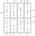
- FIGS. 17 to 26 are diagrams showing arrangement examples of the coordinate detection marks.
- the coordinate detection mark 42 is formed in a dot shape. Further, the ribs 37 are arranged so as to overlap or partially overlap. By taking the image of the coordinate detection mark 42 with the CCD 53 or the like, it is arranged so that the position where the coordinate detection mark 42 is formed on the display screen 72 can be specified mathematically or based on the encoding theory. ing.
- the coordinate detection mark 42 is formed in a rectangular or elliptical shape. Further, the rib 37 and the anode electrode as the pixel electrode are arranged so as to overlap or partially overlap.
- the coordinate detection mark 42 is arranged so that the position where the coordinate detection mark 42 is formed on the display screen 72 can be specified by capturing the image with the CCD 53 or the like. By forming the coordinate detection mark 42 on the rib 37, the pixel electrode is not shielded by the coordinate detection mark 42, and a high-luminance display is possible.
- the coordinate detection mark 42 is formed at or near the intersection of pixels. Basically, one coordinate detection mark 42 is formed with one pixel 10 or RGB pixels as one set.
- FIG. 19 shows an embodiment in which a plurality of coordinate detection marks 42 are formed for one pixel.
- the coordinate position is indicated by the number, interval, and position of the coordinate detection mark 42.
- a plurality of coordinate detection marks 42 having different shapes are arranged. Examples of the shape include a circle, a rectangle, and an ellipse. Further, the ribs 37 and the pixel electrodes are arranged so as to overlap or partially overlap.
- the coordinate detection mark 42 is arranged so that the position where the coordinate detection mark 42 is formed on the display screen 72 can be specified by capturing the image with the CCD 53 or the like.
- FIG. 21 shows an embodiment in which a plurality of coordinate detection marks 42 are formed on one pixel electrode.
- the coordinate position is indicated by the number, interval, and position of the coordinate detection mark 42.
- FIG. 22 shows an embodiment in which coordinate detection marks 42 are formed on some pixel electrodes.
- the coordinate detection mark 42 is formed in the pixel of the red pixel 10R and the blue pixel 10B, and the coordinate detection mark 42 is not formed in the green pixel 10G.
- FIG. 23 shows an embodiment in which a coordinate detection mark 42 is formed on the blue pixel 10B.
- the coordinate detection mark 42 is formed on the pixel of the blue pixel 10B, and the coordinate detection mark 42 is not formed on the red pixel 10R and the green pixel 10G.
- the alignment mark 42 a can also be used as the coordinate detection mark 42.
- the alignment mark 42a is read with the electronic pen 51, and the approximate coordinate position of the EL display panel 1 is detected.
- the shape of the coordinate detection mark 42 is preferably different from the shape and position of the alignment mark 42a.
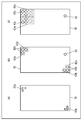
- FIG. 26 shows a modification of the alignment mark 42a.
- FIG. 26A shows an embodiment in which two alignment marks 42a are formed in one pixel.
- FIG. 26B shows an embodiment in which the alignment mark 42a is formed by combining a plurality of coordinate detection marks 42b.
- FIG. 26C shows an embodiment in which an assembly of coordinate detection marks 42c is formed in the alignment mark 42a.
- the alignment mark 42a is composed of braille characters.
- FIG. 27 is a schematic sectional view showing another example of an EL display panel in the information display device according to the embodiment.
- parallax is generated because the polarizing plate 32 and the like are arranged on the display area of the EL display panel 1. Although the pen tip of the electronic pen 51 is positioned on the polarizing plate 32, the image is displayed on the light emitting unit of the EL display panel 1, and therefore, a parallax between the pen tip and the display image occurs.
- the fiber plate 82 is bonded to the cathode electrode 39 with the adhesive layer 41, and is disposed between the polarizing plate 32 and the coordinate detection mark 42 so as to reduce parallax. It is a thing.
- the fiber plate 82 is configured by arranging a plurality of fibers 82 a having a smaller aperture than the pixel 10.
- a reflection film 82b is formed around the fiber 82a, and the refractive index is made different from that of the fiber 82a, so that the display light 83 incident on the fiber 82a is reflected and transmitted and emitted from the EL display panel 1. It is composed.
- the information display device includes the polarizing plate 32 that polarizes incident light in the EL display panel 1 including the display region 2 in which the pixels 10 of the EL elements 12 are arranged in a matrix.
- the EL display panel 1 is provided with a characteristic for changing the direction of incident light, for example, a coordinate detection mark 42 for changing the polarization state of the polarizing plate by a light scattering member or a diffraction grating.
- an electronic pen including a light generating unit such as an LED 52 that emits light such as infrared rays for detecting a coordinate detection mark, and an image acquisition unit such as a CCD 53 that captures an image of a predetermined range including the coordinate detection mark 42. If 51 is used, the coordinate position can be easily specified by detecting the light passing through the coordinate detection mark 42 or the reflected light by the image acquisition means such as the CCD 53.
- an EL display device it can be easily realized in an EL display device.
- a recording medium such as a video camera, a digital camera, a goggle type display, a navigation system, a sound reproducing device, a computer, a game machine, a portable information terminal, an image reproducing device equipped with a recording medium is reproduced and the image is displayed It can be widely applied as a display device such as a device.
- the present disclosure is useful in applying an EL display device as an information display device.
Landscapes
- Engineering & Computer Science (AREA)
- General Engineering & Computer Science (AREA)
- Theoretical Computer Science (AREA)
- Human Computer Interaction (AREA)
- Physics & Mathematics (AREA)
- General Physics & Mathematics (AREA)
- Electroluminescent Light Sources (AREA)
- Control Of Indicators Other Than Cathode Ray Tubes (AREA)
Abstract
L'invention porte sur un dispositif d'affichage d'informations qui comprend un panneau d'affichage EL comprenant : une zone d'affichage comprenant des pixels d'élément EL agencés en une matrice ; une ligne de signal de source qui fournit des signaux vidéo aux pixels ; et une ligne de signal de grille qui fournit des signaux qui commandent la sélection/désélection d'émission de lumière par les pixels. Le panneau d'affichage EL comprend une plaque de polarisation (32) qui polarise la lumière incidente, et comprend une marque de détection de coordonnées (42) possédant des propriétés qui modifient la direction de la lumière incidente.
Priority Applications (3)
| Application Number | Priority Date | Filing Date | Title |
|---|---|---|---|
| JP2013557250A JP5796091B2 (ja) | 2012-02-08 | 2012-11-22 | 情報表示装置 |
| CN201280069115.5A CN104094205B (zh) | 2012-02-08 | 2012-11-22 | 信息显示装置 |
| US14/292,460 US9588601B2 (en) | 2012-02-08 | 2014-05-30 | Information display apparatus |
Applications Claiming Priority (2)
| Application Number | Priority Date | Filing Date | Title |
|---|---|---|---|
| JP2012024702 | 2012-02-08 | ||
| JP2012-024702 | 2012-02-08 |
Related Child Applications (1)
| Application Number | Title | Priority Date | Filing Date |
|---|---|---|---|
| US14/292,460 Continuation US9588601B2 (en) | 2012-02-08 | 2014-05-30 | Information display apparatus |
Publications (1)
| Publication Number | Publication Date |
|---|---|
| WO2013118214A1 true WO2013118214A1 (fr) | 2013-08-15 |
Family
ID=48947024
Family Applications (1)
| Application Number | Title | Priority Date | Filing Date |
|---|---|---|---|
| PCT/JP2012/007520 WO2013118214A1 (fr) | 2012-02-08 | 2012-11-22 | Dispositif d'affichage d'informations |
Country Status (4)
| Country | Link |
|---|---|
| US (1) | US9588601B2 (fr) |
| JP (1) | JP5796091B2 (fr) |
| CN (1) | CN104094205B (fr) |
| WO (1) | WO2013118214A1 (fr) |
Cited By (3)
| Publication number | Priority date | Publication date | Assignee | Title |
|---|---|---|---|---|
| WO2016035239A1 (fr) * | 2014-09-01 | 2016-03-10 | パナソニックIpマネジメント株式会社 | Système de commande d'affichage |
| JP2016128884A (ja) * | 2015-01-09 | 2016-07-14 | 富士フイルム株式会社 | 透明シートを有する画像表示装置、および透明シート |
| WO2020148604A1 (fr) * | 2019-01-18 | 2020-07-23 | 株式会社半導体エネルギー研究所 | Appareil d'affichage et dispositif électronique |
Families Citing this family (8)
| Publication number | Priority date | Publication date | Assignee | Title |
|---|---|---|---|---|
| CN104701327B (zh) * | 2015-03-20 | 2018-03-02 | 京东方科技集团股份有限公司 | 阵列基板、阵列基板的制造方法和显示装置 |
| US10754442B2 (en) * | 2015-07-09 | 2020-08-25 | YewSavin, Inc. | Films or surfaces including positional tracking marks |
| JP6477910B2 (ja) * | 2016-09-16 | 2019-03-06 | 凸版印刷株式会社 | 表示装置及び表示装置基板 |
| TWI614657B (zh) * | 2016-12-16 | 2018-02-11 | 奇象光學有限公司 | 光學膜片以及使用者輸入系統 |
| US11054935B2 (en) * | 2018-11-19 | 2021-07-06 | Beechrock Limited | Stylus with contact sensor |
| CN109961694B (zh) * | 2019-02-28 | 2023-02-28 | 重庆京东方显示技术有限公司 | 一种柔性显示装置 |
| KR20210011563A (ko) * | 2019-07-22 | 2021-02-02 | 삼성디스플레이 주식회사 | 펜 감지 유닛 및 이를 포함하는 표시 장치 |
| KR20230126289A (ko) * | 2022-02-22 | 2023-08-30 | 삼성디스플레이 주식회사 | 표시 장치 및 이를 포함하는 위치 입력 시스템 |
Citations (1)
| Publication number | Priority date | Publication date | Assignee | Title |
|---|---|---|---|---|
| JP2005215676A (ja) * | 2004-01-28 | 2005-08-11 | Au Optronics Corp | 位置エンコード液晶ディスプレイパネル及び反射光散乱構造物の製造方法 |
Family Cites Families (24)
| Publication number | Priority date | Publication date | Assignee | Title |
|---|---|---|---|---|
| US4113353A (en) | 1974-04-20 | 1978-09-12 | Akira Matsushita | Information processing optical device |
| JPS50137630A (fr) * | 1974-04-20 | 1975-10-31 | ||
| JPS5644979A (en) * | 1979-09-19 | 1981-04-24 | Fujitsu Ltd | Hand-written input display |
| JPH0792723B2 (ja) | 1986-07-21 | 1995-10-09 | 株式会社日立製作所 | 座標入力装置 |
| JPH05307438A (ja) * | 1992-04-28 | 1993-11-19 | Hitachi Ltd | 情報処理装置 |
| JP3262297B2 (ja) * | 1993-04-27 | 2002-03-04 | 株式会社ワコム | 光学式座標入力装置 |
| JP3395258B2 (ja) | 1993-07-07 | 2003-04-07 | 井関農機株式会社 | コンバイン |
| JP3277052B2 (ja) | 1993-11-19 | 2002-04-22 | シャープ株式会社 | 座標入力装置、および座標入力方法 |
| SE517445C2 (sv) | 1999-10-01 | 2002-06-04 | Anoto Ab | Positionsbestämning på en yta försedd med ett positionskodningsmönster |
| EP1229353A4 (fr) | 1999-11-09 | 2006-10-11 | Omron Tateisi Electronics Co | Element reflechissant et procede de reflexion de la lumiere |
| JP4068292B2 (ja) * | 2000-09-08 | 2008-03-26 | 株式会社リコー | 情報処理システム |
| JP3523618B2 (ja) | 2001-08-02 | 2004-04-26 | シャープ株式会社 | 座標入力システムおよび座標入力システムに用いる座標パターン形成用紙 |
| JP3810725B2 (ja) | 2001-09-21 | 2006-08-16 | 株式会社半導体エネルギー研究所 | 発光装置及び電子機器 |
| JP2003256137A (ja) * | 2002-02-28 | 2003-09-10 | Kokuyo Co Ltd | ディスプレイ、透明シート |
| JP2006085679A (ja) | 2004-08-16 | 2006-03-30 | Ricoh Co Ltd | 2次元コードパターン、2次元コード作成方法、2次元コード作成装置及び印刷媒体 |
| US20090141001A1 (en) | 2005-10-17 | 2009-06-04 | Kazuo Kuroda | Display apparatus, liquid crystal display apparatus, position detection system and position detection method |
| JP3121410U (ja) * | 2006-02-22 | 2006-05-18 | 小林記録紙株式会社 | デジタルペン用読み取り用紙 |
| JP2008269545A (ja) * | 2006-06-29 | 2008-11-06 | Dainippon Printing Co Ltd | パターン印刷透明シート |
| JP2008026958A (ja) * | 2006-07-18 | 2008-02-07 | Dainippon Printing Co Ltd | 赤外線反射パターン印刷透明シート |
| JP2009037311A (ja) | 2007-07-31 | 2009-02-19 | Dainippon Printing Co Ltd | 偏光板用表面フィルム及びこれを用いた偏光板 |
| CN101609647A (zh) * | 2009-07-30 | 2009-12-23 | 友达光电股份有限公司 | 触控式有机发光二极管显示装置及影像单元 |
| KR101258258B1 (ko) * | 2009-08-27 | 2013-04-25 | 엘지디스플레이 주식회사 | 유기전계발광표시장치 |
| EP2410406A1 (fr) * | 2010-07-23 | 2012-01-25 | Anoto AB | Écran avec motif de codage |
| JP5925475B2 (ja) * | 2010-12-09 | 2016-05-25 | 株式会社半導体エネルギー研究所 | 光検出回路 |
-
2012
- 2012-11-22 WO PCT/JP2012/007520 patent/WO2013118214A1/fr active Application Filing
- 2012-11-22 JP JP2013557250A patent/JP5796091B2/ja active Active
- 2012-11-22 CN CN201280069115.5A patent/CN104094205B/zh active Active
-
2014
- 2014-05-30 US US14/292,460 patent/US9588601B2/en active Active
Patent Citations (1)
| Publication number | Priority date | Publication date | Assignee | Title |
|---|---|---|---|---|
| JP2005215676A (ja) * | 2004-01-28 | 2005-08-11 | Au Optronics Corp | 位置エンコード液晶ディスプレイパネル及び反射光散乱構造物の製造方法 |
Cited By (4)
| Publication number | Priority date | Publication date | Assignee | Title |
|---|---|---|---|---|
| WO2016035239A1 (fr) * | 2014-09-01 | 2016-03-10 | パナソニックIpマネジメント株式会社 | Système de commande d'affichage |
| JP2016128884A (ja) * | 2015-01-09 | 2016-07-14 | 富士フイルム株式会社 | 透明シートを有する画像表示装置、および透明シート |
| WO2020148604A1 (fr) * | 2019-01-18 | 2020-07-23 | 株式会社半導体エネルギー研究所 | Appareil d'affichage et dispositif électronique |
| JPWO2020148604A1 (fr) * | 2019-01-18 | 2020-07-23 |
Also Published As
| Publication number | Publication date |
|---|---|
| US20140267191A1 (en) | 2014-09-18 |
| CN104094205A (zh) | 2014-10-08 |
| US9588601B2 (en) | 2017-03-07 |
| JP5796091B2 (ja) | 2015-10-21 |
| JPWO2013118214A1 (ja) | 2015-05-11 |
| CN104094205B (zh) | 2017-03-08 |
Similar Documents
| Publication | Publication Date | Title |
|---|---|---|
| JP5796091B2 (ja) | 情報表示装置 | |
| US10579854B2 (en) | Electroluminescent display device integrated with fingerprint sensor | |
| US8199083B2 (en) | Display device | |
| JP4924393B2 (ja) | ディスプレイ装置 | |
| CN105786268B (zh) | 显示设备及其驱动方法 | |
| TWI384634B (zh) | 光學感測元件、影像裝置、電子設備和記憶元件 | |
| TWI406046B (zh) | 顯示器 | |
| JP2009032005A (ja) | 入力表示装置および入力表示パネル | |
| JP2006343713A (ja) | 液晶表示装置及びその製造方法と液晶表示装置を用いたイメージセンシング方法 | |
| JP2009139597A (ja) | 表示装置 | |
| TW201208083A (en) | Photodetector and display device | |
| JP2010097160A (ja) | 表示装置および電子機器 | |
| US11022804B2 (en) | Head-mounted display and method of controlling the same | |
| JP2009146100A (ja) | 表示装置および光センサ素子 | |
| WO2010119603A1 (fr) | Dispositif d'entrée d'écriture manuscrite | |
| JP2007241405A (ja) | 手書きシステム | |
| TW201128491A (en) | Method for driving touch panel | |
| US20100053119A1 (en) | Input/output device | |
| JP2012243201A (ja) | 入力機能付表示装置 | |
| US8242998B2 (en) | Liquid crystal display with infrared detection layer and remote control display system with same | |
| CN219832689U (zh) | 发光显示设备 | |
| JP2009063803A (ja) | 表示装置 | |
| JP2014041602A (ja) | 情報読取装置 | |
| KR102346031B1 (ko) | 표시 장치 및 이의 구동 방법 | |
| JP2010197955A (ja) | 表示装置 |
Legal Events
| Date | Code | Title | Description |
|---|---|---|---|
| 121 | Ep: the epo has been informed by wipo that ep was designated in this application |
Ref document number: 12868177 Country of ref document: EP Kind code of ref document: A1 |
|
| ENP | Entry into the national phase |
Ref document number: 2013557250 Country of ref document: JP Kind code of ref document: A |
|
| NENP | Non-entry into the national phase |
Ref country code: DE |
|
| 122 | Ep: pct application non-entry in european phase |
Ref document number: 12868177 Country of ref document: EP Kind code of ref document: A1 |