WO2020148604A1 - Appareil d'affichage et dispositif électronique - Google Patents
Appareil d'affichage et dispositif électronique Download PDFInfo
- Publication number
- WO2020148604A1 WO2020148604A1 PCT/IB2020/050102 IB2020050102W WO2020148604A1 WO 2020148604 A1 WO2020148604 A1 WO 2020148604A1 IB 2020050102 W IB2020050102 W IB 2020050102W WO 2020148604 A1 WO2020148604 A1 WO 2020148604A1
- Authority
- WO
- WIPO (PCT)
- Prior art keywords
- light
- layer
- light emitting
- transistor
- emitting device
- Prior art date
Links
- 238000006243 chemical reaction Methods 0.000 claims description 45
- 229910044991 metal oxide Inorganic materials 0.000 claims description 42
- 150000004706 metal oxides Chemical class 0.000 claims description 32
- 230000015572 biosynthetic process Effects 0.000 claims description 14
- 229910052738 indium Inorganic materials 0.000 claims description 9
- 150000002894 organic compounds Chemical class 0.000 claims description 9
- 229910052725 zinc Inorganic materials 0.000 claims description 8
- 229910052733 gallium Inorganic materials 0.000 claims description 7
- 229910052782 aluminium Inorganic materials 0.000 claims description 5
- 229910052719 titanium Inorganic materials 0.000 claims description 5
- 229910052727 yttrium Inorganic materials 0.000 claims description 5
- 229910052726 zirconium Inorganic materials 0.000 claims description 4
- 229910052684 Cerium Inorganic materials 0.000 claims description 3
- 229910052779 Neodymium Inorganic materials 0.000 claims description 3
- 229910052732 germanium Inorganic materials 0.000 claims description 3
- 229910052735 hafnium Inorganic materials 0.000 claims description 3
- 229910052746 lanthanum Inorganic materials 0.000 claims description 3
- 229910052718 tin Inorganic materials 0.000 claims description 3
- 230000035945 sensitivity Effects 0.000 abstract description 8
- 238000012905 input function Methods 0.000 abstract description 3
- 239000010410 layer Substances 0.000 description 391
- 239000004065 semiconductor Substances 0.000 description 80
- 239000000758 substrate Substances 0.000 description 76
- 239000010408 film Substances 0.000 description 69
- 239000000463 material Substances 0.000 description 37
- 239000011701 zinc Substances 0.000 description 29
- 229920005989 resin Polymers 0.000 description 25
- 239000011347 resin Substances 0.000 description 25
- 239000003990 capacitor Substances 0.000 description 23
- 239000013078 crystal Substances 0.000 description 22
- 238000000034 method Methods 0.000 description 22
- 239000012790 adhesive layer Substances 0.000 description 19
- 238000010586 diagram Methods 0.000 description 18
- 238000004519 manufacturing process Methods 0.000 description 17
- 239000011241 protective layer Substances 0.000 description 17
- 238000005192 partition Methods 0.000 description 15
- 102100022778 POC1 centriolar protein homolog A Human genes 0.000 description 13
- 101710125073 POC1 centriolar protein homolog A Proteins 0.000 description 13
- 239000000126 substance Substances 0.000 description 12
- XUIMIQQOPSSXEZ-UHFFFAOYSA-N Silicon Chemical compound [Si] XUIMIQQOPSSXEZ-UHFFFAOYSA-N 0.000 description 10
- 239000012535 impurity Substances 0.000 description 10
- 229910052710 silicon Inorganic materials 0.000 description 10
- 239000010703 silicon Substances 0.000 description 10
- IJGRMHOSHXDMSA-UHFFFAOYSA-N Atomic nitrogen Chemical compound N#N IJGRMHOSHXDMSA-UHFFFAOYSA-N 0.000 description 8
- 102100022769 POC1 centriolar protein homolog B Human genes 0.000 description 8
- 101710125069 POC1 centriolar protein homolog B Proteins 0.000 description 8
- 239000000853 adhesive Substances 0.000 description 8
- 230000001070 adhesive effect Effects 0.000 description 8
- 238000001514 detection method Methods 0.000 description 8
- QVGXLLKOCUKJST-UHFFFAOYSA-N atomic oxygen Chemical compound [O] QVGXLLKOCUKJST-UHFFFAOYSA-N 0.000 description 7
- 238000004891 communication Methods 0.000 description 7
- APFVFJFRJDLVQX-UHFFFAOYSA-N indium atom Chemical compound [In] APFVFJFRJDLVQX-UHFFFAOYSA-N 0.000 description 7
- 229910052751 metal Inorganic materials 0.000 description 7
- 239000002159 nanocrystal Substances 0.000 description 7
- 230000003287 optical effect Effects 0.000 description 7
- 229910052760 oxygen Inorganic materials 0.000 description 7
- 239000001301 oxygen Substances 0.000 description 7
- 238000012545 processing Methods 0.000 description 7
- PXHVJJICTQNCMI-UHFFFAOYSA-N Nickel Chemical group [Ni] PXHVJJICTQNCMI-UHFFFAOYSA-N 0.000 description 6
- HCHKCACWOHOZIP-UHFFFAOYSA-N Zinc Chemical compound [Zn] HCHKCACWOHOZIP-UHFFFAOYSA-N 0.000 description 6
- 230000001276 controlling effect Effects 0.000 description 6
- 238000003384 imaging method Methods 0.000 description 6
- 239000002184 metal Substances 0.000 description 6
- 230000008569 process Effects 0.000 description 6
- GYHNNYVSQQEPJS-UHFFFAOYSA-N Gallium Chemical group [Ga] GYHNNYVSQQEPJS-UHFFFAOYSA-N 0.000 description 5
- XLOMVQKBTHCTTD-UHFFFAOYSA-N Zinc monoxide Chemical compound [Zn]=O XLOMVQKBTHCTTD-UHFFFAOYSA-N 0.000 description 5
- 230000000694 effects Effects 0.000 description 5
- 239000007769 metal material Substances 0.000 description 5
- 239000002356 single layer Substances 0.000 description 5
- 238000005477 sputtering target Methods 0.000 description 5
- 229920000178 Acrylic resin Polymers 0.000 description 4
- 239000004925 Acrylic resin Substances 0.000 description 4
- XEEYBQQBJWHFJM-UHFFFAOYSA-N Iron Chemical group [Fe] XEEYBQQBJWHFJM-UHFFFAOYSA-N 0.000 description 4
- 229910052581 Si3N4 Inorganic materials 0.000 description 4
- 239000003822 epoxy resin Substances 0.000 description 4
- 239000011521 glass Substances 0.000 description 4
- 238000002347 injection Methods 0.000 description 4
- 239000007924 injection Substances 0.000 description 4
- 229910052757 nitrogen Inorganic materials 0.000 description 4
- 229920000647 polyepoxide Polymers 0.000 description 4
- -1 polyethylene terephthalate Polymers 0.000 description 4
- 229920001721 polyimide Polymers 0.000 description 4
- 230000001681 protective effect Effects 0.000 description 4
- 238000007789 sealing Methods 0.000 description 4
- HQVNEWCFYHHQES-UHFFFAOYSA-N silicon nitride Chemical compound N12[Si]34N5[Si]62N3[Si]51N64 HQVNEWCFYHHQES-UHFFFAOYSA-N 0.000 description 4
- 239000010936 titanium Substances 0.000 description 4
- RYGMFSIKBFXOCR-UHFFFAOYSA-N Copper Chemical group [Cu] RYGMFSIKBFXOCR-UHFFFAOYSA-N 0.000 description 3
- FYYHWMGAXLPEAU-UHFFFAOYSA-N Magnesium Chemical compound [Mg] FYYHWMGAXLPEAU-UHFFFAOYSA-N 0.000 description 3
- ZOKXTWBITQBERF-UHFFFAOYSA-N Molybdenum Chemical group [Mo] ZOKXTWBITQBERF-UHFFFAOYSA-N 0.000 description 3
- VYPSYNLAJGMNEJ-UHFFFAOYSA-N Silicium dioxide Chemical compound O=[Si]=O VYPSYNLAJGMNEJ-UHFFFAOYSA-N 0.000 description 3
- RTAQQCXQSZGOHL-UHFFFAOYSA-N Titanium Chemical group [Ti] RTAQQCXQSZGOHL-UHFFFAOYSA-N 0.000 description 3
- 239000000956 alloy Substances 0.000 description 3
- XAGFODPZIPBFFR-UHFFFAOYSA-N aluminium Chemical group [Al] XAGFODPZIPBFFR-UHFFFAOYSA-N 0.000 description 3
- 239000002131 composite material Substances 0.000 description 3
- 239000004020 conductor Substances 0.000 description 3
- 229910052802 copper Inorganic materials 0.000 description 3
- 239000010949 copper Chemical group 0.000 description 3
- XCJYREBRNVKWGJ-UHFFFAOYSA-N copper(II) phthalocyanine Chemical compound [Cu+2].C12=CC=CC=C2C(N=C2[N-]C(C3=CC=CC=C32)=N2)=NC1=NC([C]1C=CC=CC1=1)=NC=1N=C1[C]3C=CC=CC3=C2[N-]1 XCJYREBRNVKWGJ-UHFFFAOYSA-N 0.000 description 3
- 230000005669 field effect Effects 0.000 description 3
- 150000002484 inorganic compounds Chemical class 0.000 description 3
- 229910010272 inorganic material Inorganic materials 0.000 description 3
- 239000007788 liquid Substances 0.000 description 3
- 239000011777 magnesium Substances 0.000 description 3
- 229910052750 molybdenum Inorganic materials 0.000 description 3
- 239000011733 molybdenum Chemical group 0.000 description 3
- 229910021421 monocrystalline silicon Inorganic materials 0.000 description 3
- 229910052759 nickel Inorganic materials 0.000 description 3
- 229910021420 polycrystalline silicon Inorganic materials 0.000 description 3
- 239000009719 polyimide resin Substances 0.000 description 3
- 239000004800 polyvinyl chloride Substances 0.000 description 3
- 229920000915 polyvinyl chloride Polymers 0.000 description 3
- 239000002096 quantum dot Substances 0.000 description 3
- 238000004544 sputter deposition Methods 0.000 description 3
- WFKWXMTUELFFGS-UHFFFAOYSA-N tungsten Chemical compound [W] WFKWXMTUELFFGS-UHFFFAOYSA-N 0.000 description 3
- 229910052721 tungsten Inorganic materials 0.000 description 3
- 239000010937 tungsten Substances 0.000 description 3
- 238000001771 vacuum deposition Methods 0.000 description 3
- XLYOFNOQVPJJNP-UHFFFAOYSA-N water Substances O XLYOFNOQVPJJNP-UHFFFAOYSA-N 0.000 description 3
- VWQVUPCCIRVNHF-UHFFFAOYSA-N yttrium atom Chemical group [Y] VWQVUPCCIRVNHF-UHFFFAOYSA-N 0.000 description 3
- 239000011787 zinc oxide Substances 0.000 description 3
- XKRFYHLGVUSROY-UHFFFAOYSA-N Argon Chemical compound [Ar] XKRFYHLGVUSROY-UHFFFAOYSA-N 0.000 description 2
- 229920002284 Cellulose triacetate Polymers 0.000 description 2
- VYZAMTAEIAYCRO-UHFFFAOYSA-N Chromium Chemical compound [Cr] VYZAMTAEIAYCRO-UHFFFAOYSA-N 0.000 description 2
- 229920000089 Cyclic olefin copolymer Polymers 0.000 description 2
- KDLHZDBZIXYQEI-UHFFFAOYSA-N Palladium Chemical compound [Pd] KDLHZDBZIXYQEI-UHFFFAOYSA-N 0.000 description 2
- BQCADISMDOOEFD-UHFFFAOYSA-N Silver Chemical compound [Ag] BQCADISMDOOEFD-UHFFFAOYSA-N 0.000 description 2
- ATJFFYVFTNAWJD-UHFFFAOYSA-N Tin Chemical group [Sn] ATJFFYVFTNAWJD-UHFFFAOYSA-N 0.000 description 2
- QCWXUUIWCKQGHC-UHFFFAOYSA-N Zirconium Chemical group [Zr] QCWXUUIWCKQGHC-UHFFFAOYSA-N 0.000 description 2
- NNLVGZFZQQXQNW-ADJNRHBOSA-N [(2r,3r,4s,5r,6s)-4,5-diacetyloxy-3-[(2s,3r,4s,5r,6r)-3,4,5-triacetyloxy-6-(acetyloxymethyl)oxan-2-yl]oxy-6-[(2r,3r,4s,5r,6s)-4,5,6-triacetyloxy-2-(acetyloxymethyl)oxan-3-yl]oxyoxan-2-yl]methyl acetate Chemical compound O([C@@H]1O[C@@H]([C@H]([C@H](OC(C)=O)[C@H]1OC(C)=O)O[C@H]1[C@@H]([C@@H](OC(C)=O)[C@H](OC(C)=O)[C@@H](COC(C)=O)O1)OC(C)=O)COC(=O)C)[C@@H]1[C@@H](COC(C)=O)O[C@@H](OC(C)=O)[C@H](OC(C)=O)[C@H]1OC(C)=O NNLVGZFZQQXQNW-ADJNRHBOSA-N 0.000 description 2
- 230000001133 acceleration Effects 0.000 description 2
- 229910021417 amorphous silicon Inorganic materials 0.000 description 2
- 230000004888 barrier function Effects 0.000 description 2
- 230000000903 blocking effect Effects 0.000 description 2
- DQXBYHZEEUGOBF-UHFFFAOYSA-N but-3-enoic acid;ethene Chemical compound C=C.OC(=O)CC=C DQXBYHZEEUGOBF-UHFFFAOYSA-N 0.000 description 2
- 239000000969 carrier Substances 0.000 description 2
- 229910052804 chromium Inorganic materials 0.000 description 2
- 239000011651 chromium Substances 0.000 description 2
- 239000003086 colorant Substances 0.000 description 2
- 150000001875 compounds Chemical class 0.000 description 2
- 230000000875 corresponding effect Effects 0.000 description 2
- 229910021419 crystalline silicon Inorganic materials 0.000 description 2
- 230000007547 defect Effects 0.000 description 2
- 230000003111 delayed effect Effects 0.000 description 2
- 238000009792 diffusion process Methods 0.000 description 2
- 238000006073 displacement reaction Methods 0.000 description 2
- 230000005684 electric field Effects 0.000 description 2
- 239000005038 ethylene vinyl acetate Substances 0.000 description 2
- 238000001704 evaporation Methods 0.000 description 2
- 230000012447 hatching Effects 0.000 description 2
- 230000005525 hole transport Effects 0.000 description 2
- AMGQUBHHOARCQH-UHFFFAOYSA-N indium;oxotin Chemical compound [In].[Sn]=O AMGQUBHHOARCQH-UHFFFAOYSA-N 0.000 description 2
- 239000011261 inert gas Substances 0.000 description 2
- 239000011810 insulating material Substances 0.000 description 2
- 229910052742 iron Inorganic materials 0.000 description 2
- MRELNEQAGSRDBK-UHFFFAOYSA-N lanthanum(3+);oxygen(2-) Chemical compound [O-2].[O-2].[O-2].[La+3].[La+3] MRELNEQAGSRDBK-UHFFFAOYSA-N 0.000 description 2
- 229910052749 magnesium Inorganic materials 0.000 description 2
- 230000005389 magnetism Effects 0.000 description 2
- 230000003340 mental effect Effects 0.000 description 2
- 150000002739 metals Chemical class 0.000 description 2
- 239000000203 mixture Substances 0.000 description 2
- PLDDOISOJJCEMH-UHFFFAOYSA-N neodymium(3+);oxygen(2-) Chemical compound [O-2].[O-2].[O-2].[Nd+3].[Nd+3] PLDDOISOJJCEMH-UHFFFAOYSA-N 0.000 description 2
- 150000004767 nitrides Chemical class 0.000 description 2
- TWNQGVIAIRXVLR-UHFFFAOYSA-N oxo(oxoalumanyloxy)alumane Chemical compound O=[Al]O[Al]=O TWNQGVIAIRXVLR-UHFFFAOYSA-N 0.000 description 2
- 239000005011 phenolic resin Substances 0.000 description 2
- 239000000049 pigment Substances 0.000 description 2
- BASFCYQUMIYNBI-UHFFFAOYSA-N platinum Chemical compound [Pt] BASFCYQUMIYNBI-UHFFFAOYSA-N 0.000 description 2
- 229920001200 poly(ethylene-vinyl acetate) Polymers 0.000 description 2
- 229920002037 poly(vinyl butyral) polymer Polymers 0.000 description 2
- 229920006122 polyamide resin Polymers 0.000 description 2
- 229920000139 polyethylene terephthalate Polymers 0.000 description 2
- 239000005020 polyethylene terephthalate Substances 0.000 description 2
- 229920001343 polytetrafluoroethylene Polymers 0.000 description 2
- 239000004810 polytetrafluoroethylene Substances 0.000 description 2
- 230000005855 radiation Effects 0.000 description 2
- 229910052814 silicon oxide Inorganic materials 0.000 description 2
- 229910052709 silver Inorganic materials 0.000 description 2
- 239000004332 silver Substances 0.000 description 2
- 239000007787 solid Substances 0.000 description 2
- 238000003860 storage Methods 0.000 description 2
- 229910052715 tantalum Inorganic materials 0.000 description 2
- GUVRBAGPIYLISA-UHFFFAOYSA-N tantalum atom Chemical compound [Ta] GUVRBAGPIYLISA-UHFFFAOYSA-N 0.000 description 2
- 229910001316 Ag alloy Inorganic materials 0.000 description 1
- ZOXJGFHDIHLPTG-UHFFFAOYSA-N Boron Chemical group [B] ZOXJGFHDIHLPTG-UHFFFAOYSA-N 0.000 description 1
- XMWRBQBLMFGWIX-UHFFFAOYSA-N C60 fullerene Chemical class C12=C3C(C4=C56)=C7C8=C5C5=C9C%10=C6C6=C4C1=C1C4=C6C6=C%10C%10=C9C9=C%11C5=C8C5=C8C7=C3C3=C7C2=C1C1=C2C4=C6C4=C%10C6=C9C9=C%11C5=C5C8=C3C3=C7C1=C1C2=C4C6=C2C9=C5C3=C12 XMWRBQBLMFGWIX-UHFFFAOYSA-N 0.000 description 1
- OKTJSMMVPCPJKN-UHFFFAOYSA-N Carbon Chemical compound [C] OKTJSMMVPCPJKN-UHFFFAOYSA-N 0.000 description 1
- MYMOFIZGZYHOMD-UHFFFAOYSA-N Dioxygen Chemical compound O=O MYMOFIZGZYHOMD-UHFFFAOYSA-N 0.000 description 1
- UFHFLCQGNIYNRP-UHFFFAOYSA-N Hydrogen Chemical compound [H][H] UFHFLCQGNIYNRP-UHFFFAOYSA-N 0.000 description 1
- 206010021143 Hypoxia Diseases 0.000 description 1
- 229910000861 Mg alloy Inorganic materials 0.000 description 1
- 239000004677 Nylon Substances 0.000 description 1
- 229920012266 Poly(ether sulfone) PES Polymers 0.000 description 1
- 239000004962 Polyamide-imide Substances 0.000 description 1
- 239000004642 Polyimide Substances 0.000 description 1
- 239000004743 Polypropylene Substances 0.000 description 1
- 229920001328 Polyvinylidene chloride Polymers 0.000 description 1
- NRTOMJZYCJJWKI-UHFFFAOYSA-N Titanium nitride Chemical compound [Ti]#N NRTOMJZYCJJWKI-UHFFFAOYSA-N 0.000 description 1
- 238000009825 accumulation Methods 0.000 description 1
- NIXOWILDQLNWCW-UHFFFAOYSA-N acrylic acid group Chemical group C(C=C)(=O)O NIXOWILDQLNWCW-UHFFFAOYSA-N 0.000 description 1
- 229920000122 acrylonitrile butadiene styrene Polymers 0.000 description 1
- 230000009471 action Effects 0.000 description 1
- 229910045601 alloy Inorganic materials 0.000 description 1
- 150000001408 amides Chemical class 0.000 description 1
- 230000003321 amplification Effects 0.000 description 1
- 238000004458 analytical method Methods 0.000 description 1
- 239000004760 aramid Substances 0.000 description 1
- 229910052786 argon Inorganic materials 0.000 description 1
- 229920003235 aromatic polyamide Polymers 0.000 description 1
- 125000004429 atom Chemical group 0.000 description 1
- 230000003190 augmentative effect Effects 0.000 description 1
- UMIVXZPTRXBADB-UHFFFAOYSA-N benzocyclobutene Chemical compound C1=CC=C2CCC2=C1 UMIVXZPTRXBADB-UHFFFAOYSA-N 0.000 description 1
- 229910052790 beryllium Inorganic materials 0.000 description 1
- ATBAMAFKBVZNFJ-UHFFFAOYSA-N beryllium atom Chemical group [Be] ATBAMAFKBVZNFJ-UHFFFAOYSA-N 0.000 description 1
- 230000002457 bidirectional effect Effects 0.000 description 1
- 230000005540 biological transmission Effects 0.000 description 1
- 229910052796 boron Inorganic materials 0.000 description 1
- 239000006229 carbon black Substances 0.000 description 1
- 230000015556 catabolic process Effects 0.000 description 1
- 229920002678 cellulose Polymers 0.000 description 1
- 239000001913 cellulose Substances 0.000 description 1
- 239000000919 ceramic Substances 0.000 description 1
- ZMIGMASIKSOYAM-UHFFFAOYSA-N cerium Chemical group [Ce][Ce][Ce][Ce][Ce][Ce][Ce][Ce][Ce][Ce][Ce][Ce][Ce][Ce][Ce][Ce][Ce][Ce][Ce][Ce][Ce][Ce][Ce][Ce][Ce][Ce][Ce][Ce][Ce][Ce][Ce][Ce][Ce][Ce][Ce][Ce][Ce][Ce] ZMIGMASIKSOYAM-UHFFFAOYSA-N 0.000 description 1
- 229910000420 cerium oxide Inorganic materials 0.000 description 1
- 230000008859 change Effects 0.000 description 1
- 238000000576 coating method Methods 0.000 description 1
- 239000010941 cobalt Substances 0.000 description 1
- 229910017052 cobalt Inorganic materials 0.000 description 1
- GUTLYIVDDKVIGB-UHFFFAOYSA-N cobalt atom Chemical compound [Co] GUTLYIVDDKVIGB-UHFFFAOYSA-N 0.000 description 1
- 230000000295 complement effect Effects 0.000 description 1
- 238000011109 contamination Methods 0.000 description 1
- 229920001577 copolymer Polymers 0.000 description 1
- PMHQVHHXPFUNSP-UHFFFAOYSA-M copper(1+);methylsulfanylmethane;bromide Chemical compound Br[Cu].CSC PMHQVHHXPFUNSP-UHFFFAOYSA-M 0.000 description 1
- 230000002596 correlated effect Effects 0.000 description 1
- 238000005520 cutting process Methods 0.000 description 1
- 150000001925 cycloalkenes Chemical class 0.000 description 1
- 238000013461 design Methods 0.000 description 1
- 230000006866 deterioration Effects 0.000 description 1
- AJNVQOSZGJRYEI-UHFFFAOYSA-N digallium;oxygen(2-) Chemical compound [O-2].[O-2].[O-2].[Ga+3].[Ga+3] AJNVQOSZGJRYEI-UHFFFAOYSA-N 0.000 description 1
- 229910001882 dioxygen Inorganic materials 0.000 description 1
- KPUWHANPEXNPJT-UHFFFAOYSA-N disiloxane Chemical class [SiH3]O[SiH3] KPUWHANPEXNPJT-UHFFFAOYSA-N 0.000 description 1
- 230000009977 dual effect Effects 0.000 description 1
- 239000000428 dust Substances 0.000 description 1
- 238000005401 electroluminescence Methods 0.000 description 1
- 230000004424 eye movement Effects 0.000 description 1
- 230000008921 facial expression Effects 0.000 description 1
- 238000007667 floating Methods 0.000 description 1
- 229910003472 fullerene Inorganic materials 0.000 description 1
- 229910001195 gallium oxide Inorganic materials 0.000 description 1
- GNPVGFCGXDBREM-UHFFFAOYSA-N germanium atom Chemical group [Ge] GNPVGFCGXDBREM-UHFFFAOYSA-N 0.000 description 1
- PCHJSUWPFVWCPO-UHFFFAOYSA-N gold Chemical compound [Au] PCHJSUWPFVWCPO-UHFFFAOYSA-N 0.000 description 1
- 229910052737 gold Inorganic materials 0.000 description 1
- 239000010931 gold Substances 0.000 description 1
- 229910021389 graphene Inorganic materials 0.000 description 1
- VBJZVLUMGGDVMO-UHFFFAOYSA-N hafnium atom Chemical compound [Hf] VBJZVLUMGGDVMO-UHFFFAOYSA-N 0.000 description 1
- 229910000449 hafnium oxide Inorganic materials 0.000 description 1
- WIHZLLGSGQNAGK-UHFFFAOYSA-N hafnium(4+);oxygen(2-) Chemical compound [O-2].[O-2].[Hf+4] WIHZLLGSGQNAGK-UHFFFAOYSA-N 0.000 description 1
- 230000020169 heat generation Effects 0.000 description 1
- 239000001257 hydrogen Substances 0.000 description 1
- 229910052739 hydrogen Inorganic materials 0.000 description 1
- 150000003949 imides Chemical class 0.000 description 1
- 229910003437 indium oxide Inorganic materials 0.000 description 1
- PJXISJQVUVHSOJ-UHFFFAOYSA-N indium(iii) oxide Chemical compound [O-2].[O-2].[O-2].[In+3].[In+3] PJXISJQVUVHSOJ-UHFFFAOYSA-N 0.000 description 1
- FZLIPJUXYLNCLC-UHFFFAOYSA-N lanthanum atom Chemical group [La] FZLIPJUXYLNCLC-UHFFFAOYSA-N 0.000 description 1
- 239000000395 magnesium oxide Substances 0.000 description 1
- CPLXHLVBOLITMK-UHFFFAOYSA-N magnesium oxide Inorganic materials [Mg]=O CPLXHLVBOLITMK-UHFFFAOYSA-N 0.000 description 1
- AXZKOIWUVFPNLO-UHFFFAOYSA-N magnesium;oxygen(2-) Chemical compound [O-2].[Mg+2] AXZKOIWUVFPNLO-UHFFFAOYSA-N 0.000 description 1
- 239000011159 matrix material Substances 0.000 description 1
- 239000011156 metal matrix composite Substances 0.000 description 1
- 238000002488 metal-organic chemical vapour deposition Methods 0.000 description 1
- 229910021424 microcrystalline silicon Inorganic materials 0.000 description 1
- 239000002121 nanofiber Substances 0.000 description 1
- 239000002105 nanoparticle Substances 0.000 description 1
- QEFYFXOXNSNQGX-UHFFFAOYSA-N neodymium atom Chemical group [Nd] QEFYFXOXNSNQGX-UHFFFAOYSA-N 0.000 description 1
- 238000003199 nucleic acid amplification method Methods 0.000 description 1
- 229920001778 nylon Polymers 0.000 description 1
- 239000012044 organic layer Substances 0.000 description 1
- 230000001151 other effect Effects 0.000 description 1
- BMMGVYCKOGBVEV-UHFFFAOYSA-N oxo(oxoceriooxy)cerium Chemical compound [Ce]=O.O=[Ce]=O BMMGVYCKOGBVEV-UHFFFAOYSA-N 0.000 description 1
- SIWVEOZUMHYXCS-UHFFFAOYSA-N oxo(oxoyttriooxy)yttrium Chemical compound O=[Y]O[Y]=O SIWVEOZUMHYXCS-UHFFFAOYSA-N 0.000 description 1
- 125000004430 oxygen atom Chemical group O* 0.000 description 1
- BPUBBGLMJRNUCC-UHFFFAOYSA-N oxygen(2-);tantalum(5+) Chemical compound [O-2].[O-2].[O-2].[O-2].[O-2].[Ta+5].[Ta+5] BPUBBGLMJRNUCC-UHFFFAOYSA-N 0.000 description 1
- RVTZCBVAJQQJTK-UHFFFAOYSA-N oxygen(2-);zirconium(4+) Chemical compound [O-2].[O-2].[Zr+4] RVTZCBVAJQQJTK-UHFFFAOYSA-N 0.000 description 1
- 229910052763 palladium Inorganic materials 0.000 description 1
- 230000000737 periodic effect Effects 0.000 description 1
- 230000035699 permeability Effects 0.000 description 1
- IEQIEDJGQAUEQZ-UHFFFAOYSA-N phthalocyanine Chemical compound N1C(N=C2C3=CC=CC=C3C(N=C3C4=CC=CC=C4C(=N4)N3)=N2)=C(C=CC=C2)C2=C1N=C1C2=CC=CC=C2C4=N1 IEQIEDJGQAUEQZ-UHFFFAOYSA-N 0.000 description 1
- 230000000704 physical effect Effects 0.000 description 1
- 238000000623 plasma-assisted chemical vapour deposition Methods 0.000 description 1
- 229910052697 platinum Inorganic materials 0.000 description 1
- 229920003229 poly(methyl methacrylate) Polymers 0.000 description 1
- 229920006350 polyacrylonitrile resin Polymers 0.000 description 1
- 229920002312 polyamide-imide Polymers 0.000 description 1
- 239000004417 polycarbonate Substances 0.000 description 1
- 229920000515 polycarbonate Polymers 0.000 description 1
- 229920001225 polyester resin Polymers 0.000 description 1
- 239000004645 polyester resin Substances 0.000 description 1
- 239000011112 polyethylene naphthalate Substances 0.000 description 1
- 239000004926 polymethyl methacrylate Substances 0.000 description 1
- 229920001155 polypropylene Polymers 0.000 description 1
- 229920005591 polysilicon Polymers 0.000 description 1
- 229920001296 polysiloxane Polymers 0.000 description 1
- 229920005990 polystyrene resin Polymers 0.000 description 1
- 229920005749 polyurethane resin Polymers 0.000 description 1
- 239000005033 polyvinylidene chloride Substances 0.000 description 1
- 239000002243 precursor Substances 0.000 description 1
- 238000007639 printing Methods 0.000 description 1
- 210000001747 pupil Anatomy 0.000 description 1
- 239000010453 quartz Substances 0.000 description 1
- 239000005871 repellent Substances 0.000 description 1
- 230000004044 response Effects 0.000 description 1
- 230000002441 reversible effect Effects 0.000 description 1
- 238000005070 sampling Methods 0.000 description 1
- 239000010980 sapphire Substances 0.000 description 1
- 229910052594 sapphire Inorganic materials 0.000 description 1
- 230000035939 shock Effects 0.000 description 1
- 229920002050 silicone resin Polymers 0.000 description 1
- 238000006467 substitution reaction Methods 0.000 description 1
- 229910001936 tantalum oxide Inorganic materials 0.000 description 1
- JBQYATWDVHIOAR-UHFFFAOYSA-N tellanylidenegermanium Chemical compound [Te]=[Ge] JBQYATWDVHIOAR-UHFFFAOYSA-N 0.000 description 1
- 238000002230 thermal chemical vapour deposition Methods 0.000 description 1
- 229920001187 thermosetting polymer Polymers 0.000 description 1
- 239000010409 thin film Substances 0.000 description 1
- 238000012546 transfer Methods 0.000 description 1
- 229910052720 vanadium Inorganic materials 0.000 description 1
- GPPXJZIENCGNKB-UHFFFAOYSA-N vanadium Chemical group [V]#[V] GPPXJZIENCGNKB-UHFFFAOYSA-N 0.000 description 1
- 230000000007 visual effect Effects 0.000 description 1
- 239000011800 void material Substances 0.000 description 1
- YVTHLONGBIQYBO-UHFFFAOYSA-N zinc indium(3+) oxygen(2-) Chemical compound [O--].[Zn++].[In+3] YVTHLONGBIQYBO-UHFFFAOYSA-N 0.000 description 1
- 229910001928 zirconium oxide Inorganic materials 0.000 description 1
Images


Classifications
-
- H—ELECTRICITY
- H10—SEMICONDUCTOR DEVICES; ELECTRIC SOLID-STATE DEVICES NOT OTHERWISE PROVIDED FOR
- H10K—ORGANIC ELECTRIC SOLID-STATE DEVICES
- H10K65/00—Integrated devices, or assemblies of multiple devices, comprising at least one organic light-emitting element and at least one organic radiation-sensitive element, e.g. organic opto-couplers
-
- G—PHYSICS
- G06—COMPUTING; CALCULATING OR COUNTING
- G06F—ELECTRIC DIGITAL DATA PROCESSING
- G06F3/00—Input arrangements for transferring data to be processed into a form capable of being handled by the computer; Output arrangements for transferring data from processing unit to output unit, e.g. interface arrangements
- G06F3/01—Input arrangements or combined input and output arrangements for interaction between user and computer
- G06F3/03—Arrangements for converting the position or the displacement of a member into a coded form
- G06F3/041—Digitisers, e.g. for touch screens or touch pads, characterised by the transducing means
- G06F3/042—Digitisers, e.g. for touch screens or touch pads, characterised by the transducing means by opto-electronic means
- G06F3/0421—Digitisers, e.g. for touch screens or touch pads, characterised by the transducing means by opto-electronic means by interrupting or reflecting a light beam, e.g. optical touch-screen
-
- H—ELECTRICITY
- H10—SEMICONDUCTOR DEVICES; ELECTRIC SOLID-STATE DEVICES NOT OTHERWISE PROVIDED FOR
- H10K—ORGANIC ELECTRIC SOLID-STATE DEVICES
- H10K59/00—Integrated devices, or assemblies of multiple devices, comprising at least one organic light-emitting element covered by group H10K50/00
- H10K59/60—OLEDs integrated with inorganic light-sensitive elements, e.g. with inorganic solar cells or inorganic photodiodes
- H10K59/65—OLEDs integrated with inorganic image sensors
-
- G—PHYSICS
- G02—OPTICS
- G02B—OPTICAL ELEMENTS, SYSTEMS OR APPARATUS
- G02B5/00—Optical elements other than lenses
- G02B5/20—Filters
- G02B5/22—Absorbing filters
-
- G—PHYSICS
- G06—COMPUTING; CALCULATING OR COUNTING
- G06F—ELECTRIC DIGITAL DATA PROCESSING
- G06F3/00—Input arrangements for transferring data to be processed into a form capable of being handled by the computer; Output arrangements for transferring data from processing unit to output unit, e.g. interface arrangements
- G06F3/01—Input arrangements or combined input and output arrangements for interaction between user and computer
- G06F3/03—Arrangements for converting the position or the displacement of a member into a coded form
- G06F3/041—Digitisers, e.g. for touch screens or touch pads, characterised by the transducing means
- G06F3/0412—Digitisers structurally integrated in a display
-
- G—PHYSICS
- G09—EDUCATION; CRYPTOGRAPHY; DISPLAY; ADVERTISING; SEALS
- G09F—DISPLAYING; ADVERTISING; SIGNS; LABELS OR NAME-PLATES; SEALS
- G09F9/00—Indicating arrangements for variable information in which the information is built-up on a support by selection or combination of individual elements
- G09F9/30—Indicating arrangements for variable information in which the information is built-up on a support by selection or combination of individual elements in which the desired character or characters are formed by combining individual elements
- G09F9/33—Indicating arrangements for variable information in which the information is built-up on a support by selection or combination of individual elements in which the desired character or characters are formed by combining individual elements being semiconductor devices, e.g. diodes
-
- H—ELECTRICITY
- H05—ELECTRIC TECHNIQUES NOT OTHERWISE PROVIDED FOR
- H05B—ELECTRIC HEATING; ELECTRIC LIGHT SOURCES NOT OTHERWISE PROVIDED FOR; CIRCUIT ARRANGEMENTS FOR ELECTRIC LIGHT SOURCES, IN GENERAL
- H05B33/00—Electroluminescent light sources
- H05B33/12—Light sources with substantially two-dimensional radiating surfaces
- H05B33/14—Light sources with substantially two-dimensional radiating surfaces characterised by the chemical or physical composition or the arrangement of the electroluminescent material, or by the simultaneous addition of the electroluminescent material in or onto the light source
-
- H—ELECTRICITY
- H10—SEMICONDUCTOR DEVICES; ELECTRIC SOLID-STATE DEVICES NOT OTHERWISE PROVIDED FOR
- H10K—ORGANIC ELECTRIC SOLID-STATE DEVICES
- H10K50/00—Organic light-emitting devices
- H10K50/10—OLEDs or polymer light-emitting diodes [PLED]
- H10K50/11—OLEDs or polymer light-emitting diodes [PLED] characterised by the electroluminescent [EL] layers
-
- H—ELECTRICITY
- H10—SEMICONDUCTOR DEVICES; ELECTRIC SOLID-STATE DEVICES NOT OTHERWISE PROVIDED FOR
- H10K—ORGANIC ELECTRIC SOLID-STATE DEVICES
- H10K59/00—Integrated devices, or assemblies of multiple devices, comprising at least one organic light-emitting element covered by group H10K50/00
- H10K59/40—OLEDs integrated with touch screens
-
- G—PHYSICS
- G06—COMPUTING; CALCULATING OR COUNTING
- G06F—ELECTRIC DIGITAL DATA PROCESSING
- G06F3/00—Input arrangements for transferring data to be processed into a form capable of being handled by the computer; Output arrangements for transferring data from processing unit to output unit, e.g. interface arrangements
- G06F3/01—Input arrangements or combined input and output arrangements for interaction between user and computer
- G06F3/03—Arrangements for converting the position or the displacement of a member into a coded form
- G06F3/041—Digitisers, e.g. for touch screens or touch pads, characterised by the transducing means
- G06F3/042—Digitisers, e.g. for touch screens or touch pads, characterised by the transducing means by opto-electronic means
-
- G—PHYSICS
- G09—EDUCATION; CRYPTOGRAPHY; DISPLAY; ADVERTISING; SEALS
- G09G—ARRANGEMENTS OR CIRCUITS FOR CONTROL OF INDICATING DEVICES USING STATIC MEANS TO PRESENT VARIABLE INFORMATION
- G09G2300/00—Aspects of the constitution of display devices
- G09G2300/04—Structural and physical details of display devices
- G09G2300/0421—Structural details of the set of electrodes
- G09G2300/0426—Layout of electrodes and connections
-
- G—PHYSICS
- G09—EDUCATION; CRYPTOGRAPHY; DISPLAY; ADVERTISING; SEALS
- G09G—ARRANGEMENTS OR CIRCUITS FOR CONTROL OF INDICATING DEVICES USING STATIC MEANS TO PRESENT VARIABLE INFORMATION
- G09G2300/00—Aspects of the constitution of display devices
- G09G2300/08—Active matrix structure, i.e. with use of active elements, inclusive of non-linear two terminal elements, in the pixels together with light emitting or modulating elements
- G09G2300/0809—Several active elements per pixel in active matrix panels
- G09G2300/0814—Several active elements per pixel in active matrix panels used for selection purposes, e.g. logical AND for partial update
-
- G—PHYSICS
- G09—EDUCATION; CRYPTOGRAPHY; DISPLAY; ADVERTISING; SEALS
- G09G—ARRANGEMENTS OR CIRCUITS FOR CONTROL OF INDICATING DEVICES USING STATIC MEANS TO PRESENT VARIABLE INFORMATION
- G09G2300/00—Aspects of the constitution of display devices
- G09G2300/08—Active matrix structure, i.e. with use of active elements, inclusive of non-linear two terminal elements, in the pixels together with light emitting or modulating elements
- G09G2300/0809—Several active elements per pixel in active matrix panels
- G09G2300/0842—Several active elements per pixel in active matrix panels forming a memory circuit, e.g. a dynamic memory with one capacitor
- G09G2300/0861—Several active elements per pixel in active matrix panels forming a memory circuit, e.g. a dynamic memory with one capacitor with additional control of the display period without amending the charge stored in a pixel memory, e.g. by means of additional select electrodes
-
- G—PHYSICS
- G09—EDUCATION; CRYPTOGRAPHY; DISPLAY; ADVERTISING; SEALS
- G09G—ARRANGEMENTS OR CIRCUITS FOR CONTROL OF INDICATING DEVICES USING STATIC MEANS TO PRESENT VARIABLE INFORMATION
- G09G3/00—Control arrangements or circuits, of interest only in connection with visual indicators other than cathode-ray tubes
- G09G3/20—Control arrangements or circuits, of interest only in connection with visual indicators other than cathode-ray tubes for presentation of an assembly of a number of characters, e.g. a page, by composing the assembly by combination of individual elements arranged in a matrix no fixed position being assigned to or needed to be assigned to the individual characters or partial characters
- G09G3/22—Control arrangements or circuits, of interest only in connection with visual indicators other than cathode-ray tubes for presentation of an assembly of a number of characters, e.g. a page, by composing the assembly by combination of individual elements arranged in a matrix no fixed position being assigned to or needed to be assigned to the individual characters or partial characters using controlled light sources
- G09G3/30—Control arrangements or circuits, of interest only in connection with visual indicators other than cathode-ray tubes for presentation of an assembly of a number of characters, e.g. a page, by composing the assembly by combination of individual elements arranged in a matrix no fixed position being assigned to or needed to be assigned to the individual characters or partial characters using controlled light sources using electroluminescent panels
- G09G3/32—Control arrangements or circuits, of interest only in connection with visual indicators other than cathode-ray tubes for presentation of an assembly of a number of characters, e.g. a page, by composing the assembly by combination of individual elements arranged in a matrix no fixed position being assigned to or needed to be assigned to the individual characters or partial characters using controlled light sources using electroluminescent panels semiconductive, e.g. using light-emitting diodes [LED]
- G09G3/3208—Control arrangements or circuits, of interest only in connection with visual indicators other than cathode-ray tubes for presentation of an assembly of a number of characters, e.g. a page, by composing the assembly by combination of individual elements arranged in a matrix no fixed position being assigned to or needed to be assigned to the individual characters or partial characters using controlled light sources using electroluminescent panels semiconductive, e.g. using light-emitting diodes [LED] organic, e.g. using organic light-emitting diodes [OLED]
- G09G3/3225—Control arrangements or circuits, of interest only in connection with visual indicators other than cathode-ray tubes for presentation of an assembly of a number of characters, e.g. a page, by composing the assembly by combination of individual elements arranged in a matrix no fixed position being assigned to or needed to be assigned to the individual characters or partial characters using controlled light sources using electroluminescent panels semiconductive, e.g. using light-emitting diodes [LED] organic, e.g. using organic light-emitting diodes [OLED] using an active matrix
- G09G3/3233—Control arrangements or circuits, of interest only in connection with visual indicators other than cathode-ray tubes for presentation of an assembly of a number of characters, e.g. a page, by composing the assembly by combination of individual elements arranged in a matrix no fixed position being assigned to or needed to be assigned to the individual characters or partial characters using controlled light sources using electroluminescent panels semiconductive, e.g. using light-emitting diodes [LED] organic, e.g. using organic light-emitting diodes [OLED] using an active matrix with pixel circuitry controlling the current through the light-emitting element
Definitions
- One embodiment of the present invention relates to a display device.
- the technical field of one embodiment of the present invention includes a semiconductor device, a display device, a light-emitting device, a power storage device, a storage device, an electronic device, a lighting device, an input device (such as a touch sensor), and an input/output device (such as a touch panel). ), their driving method, or their manufacturing method can be mentioned as an example.
- a semiconductor device generally means a device that can function by utilizing semiconductor characteristics.
- a transistor and a semiconductor circuit are one mode of a semiconductor device.
- the memory device, the display device, the imaging device, and the electronic device may include a semiconductor device.
- display devices have been applied to various purposes. For example, as a large-sized display device, a home-use television device, a digital signage, a PID (Public Information Display), and the like can be given.
- a PID Public Information Display
- examples of applications of the small and medium-sized display devices include mobile information terminals such as smartphones and tablet terminals.
- Patent Document 1 discloses a light emitting device having flexibility.
- the display device is used in various devices, it is desired to have high functionality. For example, by providing a user interface function, an imaging function, and the like, a more convenient electronic device can be realized.
- One embodiment of the present invention is a display device including a light emitting device and a light receiving device in a display portion.
- One embodiment of the present invention is a display device including a first pixel, a second pixel, and a third pixel, wherein the first pixel has a first light-emitting device and a second light-emitting device.
- the third light emitting device has a second light emitting device, the third pixel has a light receiving device, the first light emitting device has a function of emitting visible light, and the second light emitting device has a near red light emitting device.
- the light receiving device has a function of emitting external light, the light receiving device has a function of detecting near-infrared light, and the second pixel generates a third potential based on the first potential and the second potential.
- the display device has a function and a function of causing the second light-emitting device to emit light in accordance with a third potential.
- the first light emitting device can have a function of emitting light of any one of red, green, blue or white.
- the light receiving device has a photoelectric conversion layer, and the photoelectric conversion layer has an organic compound.
- the first light emitting device, the second light emitting device and the light receiving device have a diode configuration, and the cathode of the first light emitting device, the cathode of the second light emitting device and the anode of the light receiving device are electrically connected. You can Alternatively, the cathode of the first light emitting device, the cathode of the second light emitting device and the cathode of the light receiving device can be electrically connected.
- a visible light cut filter is preferably provided at a position overlapping the light receiving device.
- the first to third pixels each include a transistor, the transistor includes a metal oxide in a channel formation region, and the metal oxide includes In, Zn, and M (M is Al, Ti, Ga, Ge, or Sn). , Y, Zr, La, Ce, Nd or Hf).
- a display device having an input function can be provided.
- a display device having a light detection function can be provided.
- a multifunctional display device can be provided.
- a new display device can be provided.
- a novel semiconductor device or the like can be provided.
- FIG. 1 is a diagram illustrating a display device.
- 2A to 2D and FIGS. 2E1 to 2E3 are diagrams illustrating a pixel structure.
- 2F and 2G are diagrams for explaining the arrangement of pixels.
- 2H and 2I are diagrams illustrating the configuration of the sub-pixel.
- FIG. 3A is a diagram illustrating a display device.
- 3B and 3C are diagrams for explaining the arrangement of pixels.
- FIG. 4 is a cross-sectional view illustrating a display device.
- 5A to 5C are cross-sectional views illustrating a display device.
- 6A and 6B are cross-sectional views illustrating a display device.
- 7A and 7B are cross-sectional views illustrating a display device.
- FIG. 8A and 8B are cross-sectional views illustrating a display device.
- FIG. 9 is a perspective view illustrating a display device.
- FIG. 10 is a cross-sectional view illustrating a display device.
- 11A and 11B are cross-sectional views illustrating a display device.
- 12A and 12B are cross-sectional views illustrating a display device.
- FIG. 13 is a cross-sectional view illustrating a display device.
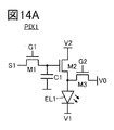
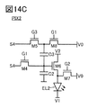
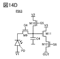
- 14A to 14D are diagrams illustrating a pixel circuit.
- FIG. 15 is a diagram illustrating a pixel circuit.
- FIG. 16 is a diagram illustrating a pixel circuit.
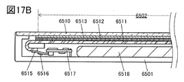
- 17A and 17B are diagrams illustrating electronic devices.
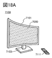
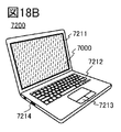
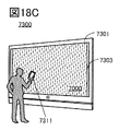
- 18A to 18D are diagrams illustrating electronic devices.
- 19A to 19F are diagrams illustrating electronic devices.
- the element may be composed of a plurality of elements.
- a plurality of transistors which operate as switches may be connected in series or in parallel.
- the capacitor may be divided and placed at a plurality of positions.
- one conductor may have a plurality of functions such as wiring, an electrode, and a terminal in some cases, and in this specification, a plurality of names may be used for the same element. Further, even if the elements are illustrated as directly connected on the circuit diagram, the elements may actually be connected via one or more conductors, In this specification, such a configuration is also included in the category of direct connection.
- One embodiment of the present invention is a display device that can perform input operation without contact.
- the display device has a first light emitting device, a second light emitting device, and a light receiving device.
- the first light emitting device has a function of displaying
- the second light emitting device has a function of emitting light for illuminating an object.
- the light receiving device has a function of detecting the light emitted from the second light emitting device and reflected by the object.
- the near touch sensor is a sensor that realizes the same function as the touch sensor in a non-contact manner.
- a booster circuit for causing the second light emitting device to emit light with high brightness is provided in the pixel having the second light emitting device.
- FIG. 1 is a diagram illustrating a display device of one embodiment of the present invention.
- the display device includes a pixel array 14, a circuit 15, a circuit 16, a circuit 17, a circuit 18, and a circuit 19.
- the pixel array 14 has pixels 10 arranged in columns and rows.
- the pixel 10 can have sub-pixels 11, 12, and 13.
- the sub-pixel 11 has a function of emitting light for display.
- the sub-pixel 12 has a function of emitting light that illuminates an object.
- the sub-pixel 13 has a function of detecting light emitted from the sub-pixel 12 and reflected by an object.
- the minimum unit in which an independent operation is performed in one "pixel” is defined as a "subpixel” for convenience of description, but the "pixel” is replaced with a “region”.
- the “sub-pixel” may be replaced with the “pixel”.
- the sub-pixel 11 has a first light emitting device that emits visible light.
- the sub-pixel 12 also has a second light emitting device that emits near infrared light.
- an EL element such as an OLED (Organic Light Emitting Diode) or a QLED (Quantum-dot Light Emitting Diode).
- a light-emitting substance included in an EL element a substance that emits fluorescence (a fluorescent material), a substance that emits phosphorescence (a phosphorescent material), a substance that exhibits thermally activated delayed fluorescence (a thermally activated delayed fluorescence: TADF) material ), inorganic compounds (quantum dot materials, etc.), and the like.
- an LED such as a micro LED (Light Emitting Diode) can be used as the light emitting device.
- the sub-pixel 13 has a light receiving device sensitive to near infrared light.
- a photoelectric conversion element that detects incident light and generates an electric charge can be used as the light receiving device.
- the amount of electric charge generated is determined based on the amount of incident light.
- a pn type or pin type photodiode can be used as the light receiving device.
- an organic photodiode having an organic compound in the photoelectric conversion layer As the light receiving device, it is preferable to use an organic photodiode having an organic compound in the photoelectric conversion layer.
- the organic photodiode is easy to be thin, lightweight and large in area. Further, since the degree of freedom in shape and design is high, it can be applied to various display devices.
- a photodiode including crystalline silicon single crystal silicon, polycrystalline silicon, microcrystalline silicon, or the like
- crystalline silicon single crystal silicon, polycrystalline silicon, microcrystalline silicon, or the like
- an organic EL element is used as a light emitting device and an organic photodiode is used as a light receiving device.
- the organic photodiode has many layers that can be configured in common with the organic EL element. Therefore, the light receiving device can be incorporated in the display device without significantly increasing the number of manufacturing steps.
- the photoelectric conversion layer of the light receiving device and the light emitting layer of the light emitting device may be separately formed, and the other layers may have the same configuration for the light emitting device and the light receiving device.
- the circuits 15 and 16 are driver circuits for driving the subpixels 11 and 12.
- the circuit 15 can function as a source driver, and the circuit 16 can function as a gate driver.
- a shift register circuit or the like can be used for the circuit 15 and the circuit 16.
- the drive circuits of the sub-pixels 11 and 12 may be separated. Since the main function of the sub-pixels 12 is to irradiate an object with light, all the sub-pixels 12 in the pixel array 14 may emit light of the same brightness. Therefore, a simplified circuit may be used instead of using a highly functional sequential circuit as a circuit corresponding to the source driver and the gate driver.
- the circuits 17 and 18 are driver circuits for driving the sub-pixel 13.
- the circuit 17 can have a function as a column driver, and the circuit 18 can have a function as a row driver.
- the circuit 19 is a circuit for reading the data output by the sub-pixel 13.
- the circuit 19 includes, for example, an A/D conversion circuit and has a function of converting analog data output from the subpixel 13 into digital data. Further, the circuit 19 may include a CDS circuit that performs correlated double sampling processing on output data.
- the sub-pixel 12 and the sub-pixel 13 can have a function as an input interface. Near-infrared light can be emitted from the sub-pixel 12, and reflected light from an object close to the display device can be received by the sub-pixel 13. Therefore, by setting a threshold value of the amount of received near-infrared light detected by the sub-pixel 13, it can function as a switch. With these, a function equivalent to that of the touch sensor can be realized without contact. Further, the operation of the pointer or the like can be performed by contact or non-contact.
- imaging data such as a fingerprint, a palm print, or an iris using the light receiving device. That is, a biometric authentication function can be added to the display device. Note that the image data may be acquired by bringing the object into contact with the display device.
- the light receiving device can be used to acquire imaging data such as a user's facial expression, eye movement, or change in pupil diameter.
- imaging data such as a user's facial expression, eye movement, or change in pupil diameter.
- the physical and mental information of the user can be acquired. Based on the information, it is possible to perform an operation according to the physical and mental condition of the user, such as changing one or both of the display and the sound output from the display device.
- These operations are effective for, for example, a VR (Virtual Reality) device, an AR (Augmented Reality) device, or an MR (Mixed Reality) device.
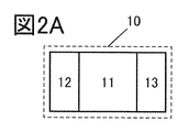
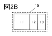
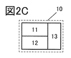
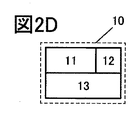
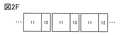
- FIGS. 2A to 2D and FIGS. 2E1 to 2E3 are diagrams illustrating an example of a layout of sub-pixels in the pixel 10.
- the sub-pixels may be arranged in the horizontal direction (the direction in which the gate lines extend).
- FIG. 1, FIG. 2C, and FIG. 2D they may be arranged in the horizontal direction and the vertical direction (direction in which the source line extends).
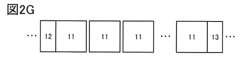
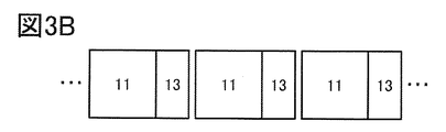
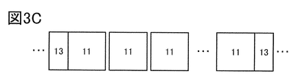
- one pixel 10 may not have the sub-pixel 13 or the sub-pixel 12.
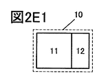
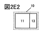
- the pixels 10 shown in FIG. 2E1 and the pixels 10 shown in FIG. 2E2 can be arranged alternately.
- the pixel 10 configured by only the sub-pixel 11 shown in FIG. 2E3 may be used.
- a plurality of pixels 10 shown in FIG. 2E3 may be provided between the pixel 10 shown in FIG. 2E1 and the pixel 10 shown in FIG. 2E2.
- the total number of sub-pixels 11 and 13 can be larger than the total number of sub-pixels 12 and 13, so that the display quality can be improved.
- the configuration and arrangement of the sub-pixels may be considered depending on the purpose.
- the number of pixels 10 in FIG. 2E1 and the number of pixels 10 in FIG. 2E2 do not have to be the same.
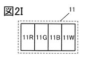
- the sub-pixel 11 is configured to emit monochromatic light, and may be a set of sub-pixels that emit different colors as shown in FIGS. 2H and 2I.
- FIG. 2H is a diagram illustrating an example in which the sub-pixel 11 includes a sub-pixel 11R having a light-emitting device that emits red, a sub-pixel 11G having a light-emitting device that emits green, and a sub-pixel 11B having a light-emitting device that emits blue. Is. Color display can be performed by using the sub-pixel 11 having the above structure.
- a subpixel 11W having a light emitting device that emits white light may be provided. Since the sub-pixel 11W can emit white light by itself, the emission brightness of the sub-pixels of other colors can be suppressed in displaying white or a color close to it. Therefore, display can be performed with low power consumption.
- the display device may be configured with the sub-pixel 11 and the sub-pixel 13 as the basic configuration of the pixel 10.
- the light source 20 for illuminating the object is arranged outside the pixel array 14 (display unit).
- the light source 20 an LED or the like that emits near-infrared light with high brightness can be used. Since the light source 20 is provided outside the pixel array 14, it can be turned on by a control different from that of the display device.
- the sub-pixels 12 are not necessary and the number of sub-pixels 13 can be increased, so that the sensitivity of object detection can be improved.
- the arrangement position and the number of the light sources 20 shown in FIG. 3A are examples, and the present invention is not limited to this.
- the light source 20 can be an element of a device including the display device of one embodiment of the present invention. Alternatively, the device may be different from the device including the display device of one embodiment of the present invention.
- pixel and sub-pixel configurations are not limited to the above, and various arrangement modes can be employed.
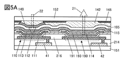
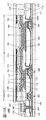
- FIG. 4 shows a schematic cross-sectional view of a display device 50A according to one embodiment of the present invention.
- the display device 50A includes a light receiving device 110, a light emitting device 190, and a light emitting device 180.
- the light receiving device 110 corresponds to an organic photodiode included in the sub-pixel 13.
- the light emitting device 190 corresponds to an organic EL element (which emits near infrared light) included in the sub-pixel 12.
- the light emitting device 180 corresponds to the organic EL element (emits visible light) included in the sub-pixel 11.
- the organic EL elements included in the sub-pixel 11 and the sub-pixel 12 and the configurations around the organic EL elements can have the same configuration except the light emitting layer. Therefore, the details of the light emitting device 190 will be described here, and the description of the light emitting device 180 will be omitted.
- the light receiving device 110 has a pixel electrode 111, a common layer 112, a photoelectric conversion layer 113, a common layer 114, and a common electrode 115.
- the light emitting device 190 has a pixel electrode 191, a common layer 112, a light emitting layer 193, a common layer 114, and a common electrode 115.
- the light emitting device 180 has a light emitting layer 183 different from the light emitting layer 193.
- the pixel electrode 111, the pixel electrode 191, the common layer 112, the photoelectric conversion layer 113, the light emitting layer 193, the common layer 114, and the common electrode 115 may each have a single-layer structure or a stacked structure.
- the pixel electrode 111 and the pixel electrode 191 are located on the insulating layer 214.
- the pixel electrode 111 and the pixel electrode 191 can be formed using the same material and the same process.
- the common layer 112 is located on the pixel electrode 111 and the pixel electrode 191.
- the common layer 112 is a layer commonly used by the light receiving device 110 and the light emitting device 190.
- the photoelectric conversion layer 113 has a region overlapping with the pixel electrode 111 with the common layer 112 interposed therebetween.
- the light emitting layer 193 has a region overlapping with the pixel electrode 191 with the common layer 112 interposed therebetween.
- the photoelectric conversion layer 113 has a first organic compound.
- the light emitting layer 193 has a second organic compound different from the first organic compound.
- the common layer 114 is located on the common layer 112, the photoelectric conversion layer 113, and the light emitting layer 193.
- the common layer 114 is a layer commonly used by the light receiving device 110 and the light emitting device 190.
- the common electrode 115 has a region overlapping with the pixel electrode 111 with the common layer 112, the photoelectric conversion layer 113, and the common layer 114 interposed therebetween. Further, the common electrode 115 has a region overlapping with the pixel electrode 191 with the common layer 112, the light emitting layer 193, and the common layer 114 interposed therebetween.
- the common electrode 115 is a layer commonly used by the light receiving device 110 and the light emitting device 190.
- an organic compound is used for the photoelectric conversion layer 113 of the light receiving device 110.
- layers other than the photoelectric conversion layer 113 can have the same configuration as the light emitting device 190 (organic EL element). Therefore, the light receiving device 110 can be formed in parallel with the formation of the light emitting device 190, only by adding the step of forming the photoelectric conversion layer 113 to the manufacturing process of the light emitting device 190. Further, the light emitting device 190 and the light receiving device 110 can be formed on the same substrate. Therefore, the light receiving device 110 can be incorporated in the display device without significantly increasing the number of manufacturing steps.
- the light receiving device 110 and the light emitting device 190 can have a common configuration except that the photoelectric conversion layer 113 of the light receiving device 110 and the light emitting layer 193 of the light emitting device 190 are separately formed.
- the configurations of the light receiving device 110 and the light emitting device 190 are not limited to this.
- the light-receiving device 110 and the light-emitting device 190 may have layers that are separately formed in addition to the photoelectric conversion layer 113 and the light-emitting layer 193 (see display devices 50C, 50D, and 50E described below).
- the light receiving device 110 and the light emitting device 190 preferably have one or more layers commonly used (common layer). Accordingly, the light receiving device 110 can be incorporated in the display device without significantly increasing the number of manufacturing steps.
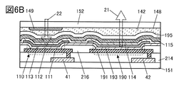
- the display device 50A includes a light receiving device 110, a light emitting device 190, a transistor 41, a transistor 42, and the like between a pair of substrates (the substrate 151 and the substrate 152).
- the common layer 112, the photoelectric conversion layer 113, and the common layer 114, which are located between the pixel electrode 111 and the common electrode 115, respectively, can be referred to as an organic layer (layer containing an organic compound).
- the pixel electrode 111 preferably has a function of reflecting near infrared light.
- the common electrode 115 has a function of transmitting visible light and near infrared light.
- the light receiving device 110 has a function of detecting light. Specifically, the light receiving device 110 is a photoelectric conversion element that converts the incident light 22 into an electric signal.
- a light shielding layer 148 is provided on the surface of the substrate 152 on the substrate 151 side.
- the light shielding layer 148 has openings at positions overlapping the light receiving device 110 and the light emitting device 190. By providing the light shielding layer 148, the range in which the light receiving device 110 detects light can be controlled.
- the light blocking layer 148 a material that blocks light emitted from the light emitting device 190 can be used.
- the light shielding layer 148 preferably absorbs visible light and near infrared light.
- the light-blocking layer 148 can be formed using, for example, a metal material, a resin material containing a pigment (such as carbon black) or a dye, or the like.
- the light shielding layer 148 may have a laminated structure of a red color filter, a green color filter, and a blue color filter.
- a filter 149 that cuts light having a shorter wavelength than the wavelength of light emitted from the light emitting device 190 (near infrared light) is provided in the opening provided in the light shielding layer 148 at a position overlapping with the light receiving device 110.
- the filter 149 for example, a long-pass filter that cuts light on the shorter wavelength side than near-infrared light, a band-pass filter that cuts at least a wavelength in the visible light region, or the like can be used.
- a semiconductor film such as an amorphous silicon thin film can be used in addition to a resin film containing a dye.
- the filter 149 may be provided so as to be laminated with the light receiving device 110, as shown in FIG. 5A.
- the filter 149 may have a lens type shape.
- the lens-type filter 149 is a convex lens having a convex surface on the substrate 151 side. Note that the substrate 152 side may be arranged so as to have a convex surface.
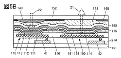
- FIG. 5B shows an example in which the lens-type filter 149 is formed first, the light shielding layer 148 may be formed first. In FIG. 5B, the end portion of the lens type filter 149 is covered with the light shielding layer 148.
- the configuration shown in FIG. 5B is a configuration in which the light 22 is incident on the light receiving device 110 via the lens type filter 149.
- the filter 149 By making the filter 149 a lens type, the image pickup range of the light receiving device 110 can be narrowed, and it is possible to prevent the image pickup range of the adjacent light receiving device 110 from overlapping. This makes it possible to capture a clear image with little blur.
- the filter 149 by forming the filter 149 into a lens shape, the opening of the light shielding layer 148 on the light receiving device 110 can be enlarged. Therefore, the amount of light incident on the light receiving device 110 can be increased, and the light detection sensitivity can be increased.
- the lens type filter 149 can be formed directly on the substrate 152 or on the light receiving device 110. Alternatively, a separately manufactured microlens array or the like may be attached to the substrate 152.
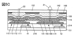
- the filter 149 may not be provided.
- the filter 149 can be omitted.
- a lens having the same shape as the lens type filter 149 shown in FIG. 5B may be provided so as to overlap the light receiving device 110.
- the lens may be made of a material that transmits visible light.
- the light receiving device 110 can detect the light 22 reflected by the object 60 such as a finger among the lights 21 emitted by the light emitting device 190 as shown in FIG. 4. However, part of the light emitted by the light emitting device 190 may be reflected in the display device 50 ⁇ /b>A and enter the light receiving device 110 without passing through the object 60.
- the light shielding layer 148 can suppress the influence of such stray light. For example, when the light shielding layer 148 is not provided, the light 23a emitted by the light emitting device 190 may be reflected by the substrate 152 and the like, and the reflected light 23b may enter the light receiving device 110. By providing the light shielding layer 148, it is possible to suppress the reflected light 23b from entering the light receiving device 110. Thereby, noise can be reduced and the light detection accuracy of the light receiving device 110 can be improved.
- the common layer 112, the light emitting layer 193, and the common layer 114 located between the pixel electrode 191 and the common electrode 115 can also be referred to as EL layers.
- the pixel electrode 191 preferably has a function of reflecting at least near infrared light.
- the light emitting device 190 has a function of emitting near infrared light. Specifically, the light emitting device 190 is an electroluminescent device that emits light 21 toward the substrate 152 side by applying a voltage between the pixel electrode 191 and the common electrode 115.
- the pixel electrode 111 is electrically connected to a source or a drain included in the transistor 41 through an opening provided in the insulating layer 214.
- the end portion of the pixel electrode 111 is covered with the partition wall 216.
- the pixel electrode 191 is electrically connected to a source or a drain included in the transistor 42 through an opening provided in the insulating layer 214.
- the end of the pixel electrode 191 is covered with a partition 216.
- the transistor 42 has a function of controlling driving of the light emitting device 190.
- the transistor 41 and the transistor 42 are in contact with each other on the same layer (the substrate 151 in FIG. 4).
- At least a part of the circuit electrically connected to the light receiving device 110 is preferably formed of the same material and the same process as the circuit electrically connected to the light emitting device 190. Accordingly, the thickness of the display device can be reduced and the manufacturing process can be simplified as compared with the case where two circuits are formed separately.
- the light receiving device 110 and the light emitting device 190 are preferably covered with a protective layer 195.
- FIG. 4 shows an example in which the protective layer 195 is provided in contact with the common electrode 115.
- the protective layer 195 impurities such as water are prevented from entering the light receiving device 110 and the light emitting device 190, and the reliability of the light receiving device 110 and the light emitting device 190 can be improved.
- the protective layer 195 and the substrate 152 are attached to each other by the adhesive layer 142.
- the protective layer 195 may not be provided on the light receiving device 110 and the light emitting device 190.
- the common electrode 115 and the substrate 152 are attached to each other by the adhesive layer 142.
- the light shielding layer 148 may not be provided. As a result, the amount of light emitted from the light emitting device 190 and the amount of light received by the light receiving device 110 can be increased, so that the detection sensitivity can be increased.
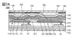
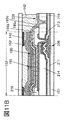
- the display device of one embodiment of the present invention may have the structure of the display device 50B illustrated in FIG. 7A.
- the display device 50B is different from the display device 50A in that the display device 50B does not have the substrate 151, the substrate 152, and the partition wall 216, but has the substrate 153, the substrate 154, the adhesive layer 155, the insulating layer 212, and the partition wall 217.
- the substrate 153 and the insulating layer 212 are attached to each other with an adhesive layer 155.
- the substrate 154 and the protective layer 195 are attached to each other with the adhesive layer 142.
- the display device 50B has a structure manufactured by transferring the insulating layer 212, the transistor 41, the transistor 42, the light-receiving device 110, the light-emitting device 190, and the like formed over the manufacturing substrate onto the substrate 153.
- the substrates 153 and 154 preferably have flexibility. Thereby, flexibility can be given to the display device 50B. For example, it is preferable to use resin for the substrates 153 and 154.
- polyester resins such as polyethylene terephthalate (PET) and polyethylene naphthalate (PEN), polyacrylonitrile resin, acrylic resin, polyimide resin, polymethylmethacrylate resin, polycarbonate (PC) resin, polyethersulfone ( PES) resin, polyamide resin (nylon, aramid, etc.), polysiloxane resin, cycloolefin resin, polystyrene resin, polyamideimide resin, polyurethane resin, polyvinyl chloride resin, polyvinylidene chloride resin, polypropylene resin, polytetrafluoroethylene (PTFE) ) Resin, ABS resin, cellulose nanofiber, etc.
- PET polyethylene terephthalate
- PEN polyethylene naphthalate
- PES polyethersulfone
- polyamide resin nylon, aramid, etc.
- polysiloxane resin cycloolefin resin
- polystyrene resin polyamideimide resin
- a film having high optical isotropy may be used for the substrate included in the display device of this embodiment.
- the film having high optical isotropy include a triacetyl cellulose (TAC, also called cellulose triacetate) film, a cycloolefin polymer (COP) film, a cycloolefin copolymer (COC) film, and an acrylic film.
- TAC triacetyl cellulose
- COP cycloolefin polymer
- COC cycloolefin copolymer
- the partition 217 is preferably capable of absorbing light emitted by the light emitting device 190.
- the partition wall 217 can be formed using, for example, a resin material containing a pigment or a dye.
- Part of the light 23c emitted by the light emitting device 190 is reflected by the substrate 152 and the partition wall 217.
- the reflected light 23d may enter the light receiving device 110.
- the light 23c may pass through the partition wall 217 and be reflected by the transistor, the wiring, or the like, so that the reflected light may enter the light receiving device 110.
- the light 23c is absorbed by the partition wall 217, so that the reflected light 23d can be suppressed from entering the light receiving device 110. Thereby, noise can be reduced and the light detection accuracy of the light receiving device 110 can be improved.
- the partition wall 217 preferably absorbs at least light having a wavelength that can be detected by the light receiving device 110.
- the light receiving device 110 detects near infrared light emitted from the light emitting device 190
- FIG. 7B shows a schematic sectional view of the display device 50C.
- the display device 50C is different from the display device 50A in that the display device 50C does not have the common layer 114 but has the buffer layer 184 and the buffer layer 194.
- the buffer layer 184 and the buffer layer 194 may have a single-layer structure or a stacked structure.
- the light receiving device 110 has a pixel electrode 111, a common layer 112, a photoelectric conversion layer 113, a buffer layer 184, and a common electrode 115.
- the light emitting device 190 includes the pixel electrode 191, the common layer 112, the light emitting layer 193, the buffer layer 194, and the common electrode 115.
- the buffer layer 184 between the common electrode 115 and the photoelectric conversion layer 113 and the buffer layer 194 between the common electrode 115 and the light emitting layer 193 are separately formed.
- the buffer layer 184 and the buffer layer 194 can be, for example, one or both of an electron injection layer and an electron transport layer.
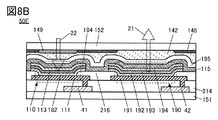
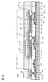
- FIG. 8A shows a schematic sectional view of the display device 50D.
- the display device 50D is different from the display device 50A in that it does not have the common layer 112 but has the buffer layer 182 and the buffer layer 192.
- the buffer layer 182 and the buffer layer 192 may have a single-layer structure or a stacked structure.
- the light receiving device 110 has a pixel electrode 111, a buffer layer 182, a photoelectric conversion layer 113, a common layer 114, and a common electrode 115.
- the light emitting device 190 has the pixel electrode 191, the buffer layer 192, the light emitting layer 193, the common layer 114, and the common electrode 115.
- the display device 50D shows an example in which the buffer layer 182 between the pixel electrode 111 and the photoelectric conversion layer 113 and the buffer layer 192 between the pixel electrode 191 and the light emitting layer 193 are separately formed.
- the buffer layer 182 and the buffer layer 192 can be, for example, one or both of a hole injection layer and a hole transport layer.
- FIG. 8B shows a schematic sectional view of the display device 50E.
- the display device 50E is different from the display device 50A in that it does not have the common layer 112 and the common layer 114 but has the buffer layer 182, the buffer layer 184, the buffer layer 192, and the buffer layer 194.
- the light receiving device 110 has a pixel electrode 111, a buffer layer 182, a photoelectric conversion layer 113, a buffer layer 184, and a common electrode 115.
- the light emitting device 190 includes the pixel electrode 191, the buffer layer 192, the light emitting layer 193, the buffer layer 194, and the common electrode 115.
- the photoelectric conversion layer 113 and the light-emitting layer 193 can be separately manufactured.
- the light receiving device 110 and the light emitting device 190 do not have a common layer between the pair of electrodes (the pixel electrode 111 or the pixel electrode 191 and the common electrode 115).
- the pixel electrode 111 and the pixel electrode 191 are formed on the insulating layer 214 by using the same material and the same process.
- the buffer layer 182, the photoelectric conversion layer 113, and the buffer layer 184 are formed over the pixel electrode 111
- the buffer layer 192, the light-emitting layer 193, and the buffer layer 194 are formed over the pixel electrode 191, and the buffer layer 184 and the buffer layer 194 are formed.
- the common electrode 115 is formed so as to cover the above.
- the manufacturing order of the stacked structure of the buffer layer 182, the photoelectric conversion layer 113, and the buffer layer 184 and the stacked structure of the buffer layer 192, the light emitting layer 193, and the buffer layer 194 is not particularly limited.
- the buffer layer 192, the light emitting layer 193, and the buffer layer 194 may be formed.
- the buffer layer 192, the light emitting layer 193, and the buffer layer 194 may be formed before forming the buffer layer 182, the photoelectric conversion layer 113, and the buffer layer 184.
- the buffer layer 182, the buffer layer 192, the photoelectric conversion layer 113, the light emitting layer 193, and the like may be alternately formed in this order.
- FIG. 9 shows a perspective view of the display device 100A.
- the display device 100A has a configuration in which a substrate 151 and a substrate 152 are attached to each other.
- the substrate 152 is shown by a broken line.
- the display device 100A includes a display portion 162, a circuit 164a, a circuit 164b, a wiring 165a, a wiring 165b, and the like.
- FIG. 9 illustrates an example in which an IC (integrated circuit) 173a, an FPC 172a, an IC 173b, and an FPC 172b are mounted on the display device 100A. Therefore, the configuration shown in FIG. 9 can be regarded as a display module including the display device 100A, the IC, and the FPC.
- a gate driver for performing display can be used as the circuit 164a.
- a low driver for performing imaging (light detection) can be used.
- the wiring 165a has a function of supplying signals and power to the subpixels 11 and 12 and the circuit 164a.
- the signal and the power are input from the outside via the FPC 172a or from the IC 173a to the wiring 165a.
- the wiring 165b has a function of supplying a signal and power to the subpixel 13 and the circuit 164b.
- the signal and the power are input from the outside via the FPC 172b or from the IC 173b to the wiring 165b.
- FIG. 9 shows an example in which the ICs 173a and 173b are provided on the substrate 151 by the COG (Chip On Glass) method, the TCP (Tape Carrier Package) method or the COF (Chip On Film) method may be used.
- the IC 173a for example, an IC having a function of a source driver connected to the subpixels 11 and 12 can be used.
- the IC 173b for example, an IC having a function of a signal processing circuit such as a column driver connected to the subpixel 13 and an A/D converter can be used.
- the driver circuit may be provided over the substrate 151 in the same manner as a transistor or the like included in a pixel circuit.
- FIG. 10 is a cross-sectional view of part of a region including the FPC 172a, part of a region including the circuit 164a, part of a region including the display portion 162, and part of a region including an end portion in the display device 100A illustrated in FIG. An example is shown.
- a display device 100A illustrated in FIG. 10 includes a transistor 201, a transistor 205, a transistor 206, a light emitting device 190, a light receiving device 110, and the like between a substrate 151 and a substrate 152.
- the substrate 152 and the insulating layer 214 are adhered to each other via the adhesive layer 142.
- a solid sealing structure, a hollow sealing structure, or the like can be applied to seal the light emitting device 190 and the light receiving device 110.
- a space 143 surrounded by the substrate 152, the adhesive layer 142, and the insulating layer 214 is filled with an inert gas (nitrogen, argon, etc.), and a hollow sealing structure is applied.
- the adhesive layer 142 may be provided so as to overlap with the light emitting device 190. Further, the region surrounded by the substrate 152, the adhesive layer 142, and the insulating layer 214 may be filled with a resin different from that of the adhesive layer 142.
- the light emitting device 190 has a laminated structure in which the pixel electrode 191, the common layer 112, the light emitting layer 193, the common layer 114, and the common electrode 115 are laminated in this order from the insulating layer 214 side.
- the pixel electrode 191 is connected to the conductive layer 222b included in the transistor 206 through an opening provided in the insulating layer 214.
- the transistor 206 has a function of controlling driving of the light emitting device 190.
- the end of the pixel electrode 191 is covered with a partition 216.
- the light receiving device 110 has a laminated structure in which the pixel electrode 111, the common layer 112, the photoelectric conversion layer 113, the common layer 114, and the common electrode 115 are laminated in this order from the insulating layer 214 side.
- the pixel electrode 111 is electrically connected to the conductive layer 222b included in the transistor 205 through an opening provided in the insulating layer 214.
- the end portion of the pixel electrode 111 is covered with the partition wall 216.
- the light emitted from the light emitting device 190 is emitted to the substrate 152 side. Further, light is incident on the light receiving device 110 through the substrate 152 and the space 143.
- the substrate 152 it is preferable to use a material having high transparency to visible light and near infrared light.
- the pixel electrode 111 and the pixel electrode 191 can be manufactured using the same material and the same process.
- the common layer 112, the common layer 114, and the common electrode 115 are used for both the light receiving device 110 and the light emitting device 190.
- the light receiving device 110 and the light emitting device 190 may have a common configuration except that the configurations of the photoelectric conversion layer 113 and the light emitting layer 193 are different. Accordingly, the light receiving device 110 can be built in the display device 100A without significantly increasing the number of manufacturing steps.
- a light shielding layer 148 is provided on the surface of the substrate 152 on the substrate 151 side.
- the light shielding layer 148 has openings at positions overlapping the light receiving device 110 and light emitting device 190.
- a filter 149 that cuts visible light is provided at a position overlapping the light receiving device 110. Note that the filter 149 may not be provided.
- the transistor 201, the transistor 205, and the transistor 206 are all formed over the substrate 151. These transistors can be manufactured using the same material and the same process.
- An insulating layer 211, an insulating layer 213, an insulating layer 215, and an insulating layer 214 are provided in this order over the substrate 151.
- Part of the insulating layer 211 functions as a gate insulating layer of each transistor.
- Part of the insulating layer 213 functions as a gate insulating layer of each transistor.
- the insulating layer 215 is provided so as to cover the transistor.
- the insulating layer 214 is provided so as to cover the transistor and has a function as a planarization layer. Note that the number of gate insulating layers and the number of insulating layers covering the transistor are not limited, and each may be a single layer or two or more layers.
- a material in which impurities such as water and hydrogen do not easily diffuse for at least one insulating layer that covers the transistor. This allows the insulating layer to function as a barrier layer. With such a structure, diffusion of impurities into the transistor from the outside can be effectively suppressed, and reliability of the display device can be improved.
- an inorganic insulating film for example, a silicon nitride film, a silicon oxynitride film, a silicon oxide film, a silicon nitride oxide film, an aluminum oxide film, or an aluminum nitride film can be used.
- a hafnium oxide film, a yttrium oxide film, a zirconium oxide film, a gallium oxide film, a tantalum oxide film, a magnesium oxide film, a lanthanum oxide film, a cerium oxide film, or a neodymium oxide film may be used.
- two or more of the above-mentioned insulating films may be laminated and used.
- An organic insulating film is suitable for the insulating layer 214 which functions as a planarization layer.
- Materials that can be used for the organic insulating film include acrylic resin, polyimide resin, epoxy resin, polyamide resin, polyimide amide resin, siloxane resin, benzocyclobutene resin, phenol resin, and precursors of these resins. ..
- the organic insulating film often has a lower barrier property against impurities than the inorganic insulating film. Therefore, the organic insulating film preferably has an opening near the end of the display device 100A. This can prevent impurities from diffusing from the end of the display device 100A through the organic insulating film.
- the organic insulating film may be formed so that the end portion of the organic insulating film is located inside the end portion of the display device 100A so that the organic insulating film is not exposed at the end portion of the display device 100A.
- an opening is formed in the insulating layer 214. Accordingly, even when an organic insulating film is used for the insulating layer 214, it is possible to prevent impurities from diffusing from the outside to the display portion 162 through the insulating layer 214. Therefore, the reliability of the display device 100A can be improved.
- the transistor 201, the transistor 205, and the transistor 206 each include a conductive layer 221 functioning as a gate, an insulating layer 211 functioning as a gate insulating layer, conductive layers 222a and 222b functioning as a source and a drain, a semiconductor layer 231, and a gate insulating layer.
- the insulating layer 213 that functions as a gate and the conductive layer 223 that functions as a gate are included.
- the same hatching pattern is given to a plurality of layers obtained by processing the same conductive film.
- the insulating layer 211 is located between the conductive layer 221 and the semiconductor layer 231.
- the insulating layer 213 is located between the conductive layer 223 and the semiconductor layer 231.
- the structure of the transistor included in the display device of this embodiment is not particularly limited.
- a planar transistor, a staggered transistor, an inverted staggered transistor, or the like can be used.
- either a top-gate or bottom-gate transistor structure may be used.
- gates may be provided above and below a semiconductor layer in which a channel is formed.
- a structure in which a semiconductor layer in which a channel is formed is sandwiched between two gates is applied to the transistor 201, the transistor 205, and the transistor 206.
- the transistor may be driven by connecting two gates and supplying the same signal to them.
- one of the two gates may be supplied with a potential for controlling the threshold voltage of the transistor and the other may be supplied with a potential for driving.
- the crystallinity of a semiconductor material used for a transistor is not particularly limited, and an amorphous semiconductor, a single crystal semiconductor, or a semiconductor having crystallinity other than single crystal (a microcrystalline semiconductor, a polycrystalline semiconductor, or a part of which has a crystalline region). Any of the above semiconductors) may be used. It is preferable to use a single crystal semiconductor or a semiconductor having crystallinity because deterioration of transistor characteristics can be suppressed.
- the semiconductor layer of the transistor preferably contains a metal oxide (also referred to as an oxide semiconductor).
- the semiconductor layer of the transistor may include silicon. Examples of silicon include amorphous silicon and crystalline silicon (low temperature polysilicon, single crystal silicon, etc.).
- the semiconductor layer is, for example, indium and M (M is gallium, aluminum, silicon, boron, yttrium, tin, copper, vanadium, beryllium, titanium, iron, nickel, germanium, zirconium, molybdenum, lanthanum, cerium, neodymium, It is preferable to have zinc and one or more kinds selected from hafnium, tantalum, tungsten, and magnesium).
- M is preferably one or more selected from aluminum, gallium, yttrium, and tin.
- an oxide containing indium (In), gallium (Ga), and zinc (Zn) (also referred to as IGZO) is preferably used for the semiconductor layer.
- the atomic ratio of In in the sputtering target is preferably greater than or equal to the atomic ratio of M.
- the atomic ratio of the semiconductor layer to be formed includes a fluctuation of ⁇ 40% in the atomic ratio of the metal element contained in the sputtering target.
- the atomic ratio of Ga is larger than 0.1. It is 2 or less and includes the case where the atomic ratio of Zn is 5 or more and 7 or less.
- the transistor included in the circuit 164a and the transistor included in the display portion 162 may have the same structure or different structures.
- the structures of the plurality of transistors included in the circuit 164a may be all the same or may be two or more.
- the structures of the plurality of transistors included in the display portion 162 may be all the same or may be two or more.
- connection portion 204 is provided in a region of the substrate 151 where the substrates 152 do not overlap.
- the wiring 165 is electrically connected to the FPC 172a via the conductive layer 166 and the connection layer 242.
- the conductive layer 166 obtained by processing the same conductive film as the pixel electrode 191 is exposed. Accordingly, the connection portion 204 and the FPC 172a can be electrically connected via the connection layer 242.
- optical members can be arranged outside the substrate 152.
- the optical member include a polarizing plate, a retardation plate, a light diffusing layer (such as a diffusing film), an antireflection layer, and a light collecting film.
- a polarizing plate a retardation plate
- a light diffusing layer such as a diffusing film
- an antireflection layer e.g., a light collecting film.
- an antistatic film that suppresses adhesion of dust
- a water-repellent film that prevents adhesion of dirt
- a hard coat film that suppresses the generation of scratches during use
- a shock absorbing layer arranged. May be.
- the substrate 151 and the substrate 152 glass, quartz, ceramic, sapphire, resin, or the like can be used.
- various curable adhesives such as a photo-curable adhesive such as an ultraviolet curable adhesive, a reaction curable adhesive, a thermosetting adhesive, and an anaerobic adhesive can be used.
- these adhesives include epoxy resin, acrylic resin, silicone resin, phenol resin, polyimide resin, imide resin, PVC (polyvinyl chloride) resin, PVB (polyvinyl butyral) resin, EVA (ethylene vinyl acetate) resin, and the like.
- a material having low moisture permeability such as epoxy resin is preferable.
- a two-liquid mixed type resin may be used.
- an adhesive sheet or the like may be used.
- an anisotropic conductive film (ACF: Anisotropic Conductive Film), an anisotropic conductive paste (ACP: Anisotropic Conductive Paste), or the like can be used.
- ACF Anisotropic Conductive Film
- ACP Anisotropic Conductive Paste
- the light emitting device 190 may be a top emission type, a bottom emission type, a dual emission type, or the like. In one embodiment of the present invention, a top emission type is preferable, but another structure can be applied by making the light emitting surface of the light emitting device 190 and the light incident surface of the light receiving device 110 have the same direction. Can also
- the light emitting device 190 has at least a light emitting layer 193.
- a substance having a high hole injecting property a substance having a high hole transporting property, a hole blocking material, a substance having a high electron transporting property, a substance having a high electron injecting property or a bipolar property.
- It may further have a layer containing a substance (a substance having a high electron transporting property and a high hole transporting property) or the like.
- the common layer 112 preferably has one or both of a hole injection layer and a hole transport layer.
- the common layer 114 preferably has one or both of an electron transport layer and an electron injection layer.
- the common layer 112, the light emitting layer 193, and the common layer 114 either a low molecular compound or a high molecular compound can be used, and an inorganic compound may be contained.
- the layers forming the common layer 112, the light emitting layer 193, and the common layer 114 can be formed by a method such as an evaporation method (including a vacuum evaporation method), a transfer method, a printing method, an inkjet method, a coating method, or the like.
- the light emitting layer 193 may have an inorganic compound such as a quantum dot as a light emitting material.
- the photoelectric conversion layer 113 of the light receiving device 110 includes a semiconductor.
- the semiconductor an inorganic semiconductor such as silicon or an organic semiconductor containing an organic compound can be used.
- an organic semiconductor as a semiconductor included in the photoelectric conversion layer 113 is described.
- the light emitting layer 193 of the light emitting device 190 and the photoelectric conversion layer 113 of the light receiving device 110 can be formed by the same method (for example, a vacuum evaporation method), and the manufacturing apparatus can be shared. preferable.
- Examples of the n-type semiconductor material included in the photoelectric conversion layer 113 include electron-accepting organic semiconductor materials such as fullerenes (for example, C 60 , C 70, etc.) and their derivatives.
- examples of a p-type semiconductor material included in the photoelectric conversion layer 113 include copper(II) phthalocyanine (Copper(II) phthalocyanine; CuPc), tetraphenyldibenzoperifuranthene (DBP), and zinc phthalocyanine (Zinc Phanthalkane).
- CuPc copper(II) phthalocyanine
- DBP tetraphenyldibenzoperifuranthene
- Zinc Phanthalkane zinc phthalocyanine
- the photoelectric conversion layer 113 can be formed by co-evaporating an n-type semiconductor and a p-type semiconductor.
- Materials that can be used for conductive layers such as gates, sources, and drains of transistors as well as various wirings and electrodes that configure a display device include aluminum, titanium, chromium, nickel, copper, yttrium, zirconium, molybdenum, silver, and Examples thereof include metals such as tantalum and tungsten, and alloys containing the metals as main components. A film containing any of these materials can be used as a single-layer structure or a laminated structure.
- a conductive oxide such as indium oxide, indium tin oxide, indium zinc oxide, zinc oxide, or zinc oxide containing gallium, or graphene
- a metal material such as gold, silver, platinum, magnesium, nickel, tungsten, chromium, molybdenum, iron, cobalt, copper, palladium, and titanium, or an alloy material containing the metal material
- a nitride of the metal material for example, titanium nitride
- a stacked film of any of the above materials can be used as the conductive layer.
- a stacked film of an alloy of silver and magnesium and indium tin oxide is preferably used because conductivity can be increased.
- These can also be used for various wirings forming a display device, a conductive layer such as an electrode, and a conductive layer included in a display element (a conductive layer functioning as a pixel electrode or a common electrode).
- Examples of insulating materials that can be used for each insulating layer include resins such as acrylic resin and epoxy resin, and inorganic insulating materials such as silicon oxide, silicon oxynitride, silicon nitride oxide, silicon nitride, and aluminum oxide.
- FIG. 11A shows a sectional view of the display device 100B.
- the display device 100B mainly differs from the display device 100A in that it has a protective layer 195.
- the protective layer 195 that covers the light receiving device 110 and the light emitting device 190, it is possible to suppress the diffusion of impurities such as water into the light receiving device 110 and the light emitting device 190, and improve the reliability of the light receiving device 110 and the light emitting device 190. You can
- the insulating layer 215 and the protective layer 195 are preferably in contact with each other through the opening in the insulating layer 214.
- the inorganic insulating film of the insulating layer 215 and the inorganic insulating film of the protective layer 195 are preferably in contact with each other. This can prevent impurities from diffusing from the outside into the display unit 162 through the organic insulating film. Therefore, the reliability of the display device 100B can be improved.
- FIG. 11B shows an example in which the protective layer 195 has a three-layer structure.
- the protective layer 195 includes an inorganic insulating layer 195a on the common electrode 115, an organic insulating layer 195b on the inorganic insulating layer 195a, and an inorganic insulating layer 195c on the organic insulating layer 195b.
- the end portion of the inorganic insulating layer 195a and the end portion of the inorganic insulating layer 195c extend outside the end portion of the organic insulating layer 195b and are in contact with each other. Then, the inorganic insulating layer 195a is in contact with the insulating layer 215 (inorganic insulating layer) through the opening of the insulating layer 214 (organic insulating layer). Accordingly, since the light receiving device 110 and the light emitting device 190 can be surrounded by the insulating layer 215 and the protective layer 195, the reliability of the light receiving device 110 and the light emitting device 190 can be improved.
- the protective layer 195 may have a laminated structure of an organic insulating film and an inorganic insulating film. At this time, it is preferable to extend the end portion of the inorganic insulating film outside the end portion of the organic insulating film.
- the protective layer 195 and the substrate 152 are attached to each other with the adhesive layer 142.
- the adhesive layer 142 is provided so as to overlap the light receiving device 110 and the light emitting device 190, respectively, and a solid sealing structure is applied to the display device 100B.
- FIG. 12A shows a sectional view of the display device 100C.
- the display device 100C mainly differs from the display device 100B in that the structure of the transistor is different and that the light shielding layer 148 is not provided.
- the display device 100C includes the transistor 208, the transistor 209, and the transistor 210 over the substrate 151.
- the transistor 208, the transistor 209, and the transistor 210 each include a conductive layer 221 functioning as a gate, an insulating layer 211 functioning as a gate insulating layer, a semiconductor layer having a channel formation region 231i and a pair of low resistance regions 231n, and a pair of low resistance layers.
- An insulating layer 215 which covers the layer 223 is included.
- the insulating layer 211 is located between the conductive layer 221 and the channel formation region 231i.
- the insulating layer 225 is located between the conductive layer 223 and the channel formation region 231i.
- the conductive layers 222a and 222b are connected to the low resistance region 231n through the openings provided in the insulating layer 225 and the insulating layer 215, respectively.
- One of the conductive layers 222a and 222b functions as a source and the other functions as a drain.
- the pixel electrode 191 of the light emitting device 190 is electrically connected to one of the pair of low resistance regions 231n of the transistor 208 through the conductive layer 222b.
- the pixel electrode 111 of the light receiving device 110 is electrically connected to the other of the pair of low resistance regions 231n of the transistor 209 via the conductive layer 222b.
- FIG. 12A shows an example in which the insulating layer 225 covers the top surface and the side surface of the semiconductor layer.
- FIG. 12B shows an example in which the insulating layer 225 overlaps the channel formation region 231i of the semiconductor layer 231 and does not overlap the low resistance region 231n.
- the structure shown in FIG. 12B can be manufactured by processing the insulating layer 225 using the conductive layer 223 as a mask.
- the insulating layer 215 is provided so as to cover the insulating layer 225 and the conductive layer 223, and the conductive layer 222a and the conductive layer 222b are connected to the low resistance region 231n through the openings of the insulating layer 215, respectively.
- an insulating layer 218 which covers the transistor may be provided.
- FIG. 13 shows a cross-sectional view of the display device 100D.
- the display device 100D mainly differs from the display device 100C in that the configuration of the substrate is different.
- the display device 100D does not include the substrate 151 and the substrate 152, but includes the substrate 153, the substrate 154, the adhesive layer 155, and the insulating layer 212.
- the substrate 153 and the insulating layer 212 are attached to each other with an adhesive layer 155.
- the substrate 154 and the protective layer 195 are attached to each other with the adhesive layer 142.
- the display device 100D has a structure in which the insulating layer 212, the transistor 208, the transistor 209, the light-receiving device 110, the light-emitting device 190, and the like formed over the manufacturing substrate are transferred to the substrate 153.
- the substrates 153 and 154 preferably have flexibility. Thereby, flexibility can be provided to the display device 100D.
- the insulating layer 212 an inorganic insulating film which can be used for the insulating layer 211, the insulating layer 213, and the insulating layer 215 can be used.
- the insulating layer 212 may be a stacked film of an organic insulating film and an inorganic insulating film.
- the film on the transistor 209 side is preferably an inorganic insulating film.
- the display device of this embodiment has a light receiving device and a light emitting device in a display portion, and the display portion has both a function of displaying an image and a function of detecting light. This makes it possible to reduce the size and weight of the electronic device as compared with the case where the sensor is provided outside the display unit or outside the display device. Further, a multifunctional electronic device can be realized by combining with a sensor provided outside the display portion or outside the display device.
- At least one layer other than the photoelectric conversion layer of the light receiving device can be configured in common with the light emitting device (EL element). Further, in the light receiving device, all layers other than the photoelectric conversion layer may have the same configuration as the light emitting device (EL element). For example, the light emitting device and the light receiving device can be formed on the same substrate only by adding a step of forming a photoelectric conversion layer to the manufacturing process of the light emitting device. Further, in the light receiving device and the light emitting device, the pixel electrode and the common electrode can be formed by using the same material and the same process.
- the manufacturing process of the display device can be simplified. In this way, a light-emitting device can be built in and a highly convenient display device can be manufactured without complicated steps.
- the metal oxide applicable to the semiconductor layer of the transistor will be described below.
- metal oxides containing nitrogen may be collectively referred to as metal oxides. Further, the metal oxide containing nitrogen may be referred to as a metal oxynitride. For example, a metal oxide containing nitrogen such as zinc oxynitride (ZnON) may be used for the semiconductor layer.
- ZnON zinc oxynitride
- CAAC c-axis aligned aligned crystal
- CAC Cloud-Aligned composite
- CAC Cloud-Aligned Composite
- OS Oxide Semiconductor
- the CAC-OS or the CAC-metal oxide has a conductive function in a part of the material and an insulating function in a part of the material, and the whole material has a function as a semiconductor.
- a conductive function is a function of flowing electrons (or holes) serving as carriers
- an insulating function is an electron serving as carriers. It is a function that does not flow.
- the CAC-OS or the CAC-metal oxide has a conductive region and an insulating region.
- the conductive region has the above-mentioned conductive function
- the insulating region has the above-mentioned insulating function.
- the conductive region and the insulating region may be separated at the nanoparticle level.
- the conductive region and the insulating region may be unevenly distributed in the material.
- the conductive region may be observed by blurring the periphery and connecting in a cloud shape.
- the conductive region and the insulating region are dispersed in the material in a size of 0.5 nm or more and 10 nm or less, preferably 0.5 nm or more and 3 nm or less. There is.
- the CAC-OS or CAC-metal oxide is composed of components having different band gaps.
- CAC-OS or CAC-metal oxide is composed of a component having a wide gap due to the insulating region and a component having a narrow gap due to the conductive region.
- the carrier when the carrier flows, the carrier mainly flows in the component having the narrow gap.
- the component having the narrow gap acts complementarily to the component having the wide gap, and the carrier also flows in the component having the wide gap in conjunction with the component having the narrow gap. Therefore, when the CAC-OS or CAC-metal oxide is used in the channel formation region of the transistor, a high current driving force, that is, a high on-current and a high field-effect mobility can be obtained in the on state of the transistor.
- the CAC-OS or the CAC-metal oxide can also be referred to as a matrix composite material or a metal matrix composite material.
- the oxide semiconductor (metal oxide) is classified into a single crystal oxide semiconductor and a non-single crystal oxide semiconductor other than the single crystal oxide semiconductor.
- the non-single-crystal oxide semiconductor include a CAAC-OS (c-axis aligned crystal line oxide semiconductor), a polycrystalline oxide semiconductor, an nc-OS (nanocrystal oxide semiconductor), and a pseudo-amorphous oxide semiconductor (a-like oxide).
- OS amorphous-like oxide semiconductor), and amorphous oxide semiconductor.
- the CAAC-OS has a c-axis orientation and has a crystal structure in which a plurality of nanocrystals are connected in the ab plane direction and have distortion.
- the strain refers to a portion in which the orientation of the lattice arrangement is changed between a region where the lattice arrangement is uniform and another region where the lattice arrangement is uniform in the region where the plurality of nanocrystals are connected.
- the nanocrystal is basically a hexagon, but is not limited to a regular hexagon, and may be a non-regular hexagon.
- the strain may have a lattice arrangement such as a pentagon and a heptagon.
- a lattice arrangement such as a pentagon and a heptagon.
- the CAAC-OS is a layered crystal in which a layer containing indium and oxygen (hereinafter, an In layer) and a layer containing elements M, zinc, and oxygen (hereinafter, a (M,Zn) layer) are stacked. It tends to have a structure (also called a layered structure). Note that indium and the element M can be replaced with each other, and when the element M of the (M,Zn) layer is replaced with indium, it can be expressed as an (In,M,Zn) layer. When the indium in the In layer is replaced with the element M, it can be expressed as an (In,M) layer.
- CAAC-OS is a metal oxide with high crystallinity.
- CAAC-OS since it is difficult to confirm a clear crystal grain boundary, it can be said that a decrease in electron mobility due to the crystal grain boundary does not easily occur.
- CAAC-OS impurities and defects oxygen deficiency (V O:. Oxygen vacancy also referred) etc.) with less metal It can be said to be an oxide. Therefore, the metal oxide having CAAC-OS has stable physical properties. Therefore, the metal oxide containing CAAC-OS is highly heat resistant and highly reliable.
- the nc-OS has a periodic atomic arrangement in a minute region (for example, a region of 1 nm or more and 10 nm or less, particularly a region of 1 nm or more and 3 nm or less). Moreover, in the nc-OS, no regularity is found in the crystal orientation between different nanocrystals. Therefore, no orientation is seen in the entire film. Therefore, the nc-OS may be indistinguishable from the a-like OS or the amorphous oxide semiconductor depending on the analysis method.
- IGZO indium-gallium-zinc oxide
- IGZO indium-gallium-zinc oxide
- IGZO may have a stable structure by using the above-described nanocrystal.
- IGZO tends to have difficulty in crystal growth in the atmosphere, and thus a smaller crystal (for example, the above-mentioned nanocrystal) is used than a large crystal (here, a crystal of several mm or a crystal of several cm).
- a large crystal here, a crystal of several mm or a crystal of several cm.
- it may be structurally stable.
- the a-like OS is a metal oxide having a structure between the nc-OS and the amorphous oxide semiconductor.
- the a-like OS has a void or a low density region. That is, the crystallinity of the a-like OS is lower than that of the nc-OS and the CAAC-OS.
- Oxide semiconductors have various structures and have different characteristics.
- the oxide semiconductor of one embodiment of the present invention may include two or more of an amorphous oxide semiconductor, a polycrystalline oxide semiconductor, an a-like OS, an nc-OS, and a CAAC-OS.
- the metal oxide film functioning as a semiconductor layer can be formed by a sputtering method using one or both of an inert gas and an oxygen gas.
- an inert gas oxygen gas
- oxygen flow rate ratio oxygen partial pressure
- the flow rate ratio of oxygen (oxygen partial pressure) during the formation of the metal oxide film is preferably 0% to 30%, preferably 5% to 30%. Is more preferable and 7% or more and 15% or less is still more preferable.
- the energy gap of the metal oxide is preferably 2 eV or more, more preferably 2.5 eV or more, and further preferably 3 eV or more.
- the transistor including the above metal oxide can exhibit extremely low off-state current of several yA/ ⁇ m (current value per 1 ⁇ m of channel width).
- a transistor including a metal oxide has characteristics different from those of a transistor including Si in that impact ionization, avalanche breakdown, short channel effect, and the like do not occur, and a highly reliable circuit can be formed. ..
- variation in electrical characteristics due to nonuniform crystallinity, which is a problem in a transistor including Si is less likely to occur in a transistor including a metal oxide.
- the substrate temperature during the formation of the metal oxide film is preferably 350° C. or lower, more preferably room temperature or higher and 200° C. or lower, still more preferably room temperature or higher and 130° C. or lower.
- productivity can be improved, which is preferable.
- the metal oxide film can be formed by a sputtering method, a PLD method, a PECVD method, a thermal CVD method, a MOCVD method, an ALD method, a vacuum evaporation method, or the like.
- a pixel of the display device of one embodiment of the present invention includes subpixels 11, 12, and 13.
- the pixel circuit PIX1 of the sub-pixel 11 has a light emitting device that emits visible light.
- the pixel circuit PIX2 of the sub-pixel 12 has a light emitting device that emits near infrared light.
- the pixel circuit PIX3 of the sub-pixel 13 has a light receiving device.
- FIG. 14A shows an example of the pixel circuit PIX1 of the sub-pixel 11.
- the pixel circuit PIX1 has a light emitting device EL1, a transistor M1, a transistor M2, a transistor M3, and a capacitor C1.
- a light emitting diode is used as the light emitting device EL1
- An organic EL element that emits visible light is preferably used for the light emitting device EL1.
- a gate is electrically connected to the wiring G1
- one of a source and a drain is electrically connected to the wiring S1
- the other of the source and the drain is electrically connected to one electrode of the capacitor C1 and a gate of the transistor M2.
- One of a source and a drain of the transistor M2 is electrically connected to the wiring V2, and the other is electrically connected to an anode of the light emitting device EL1 and one of a source and a drain of the transistor M3.
- a gate of the transistor M3 is electrically connected to the wiring G2, and the other of the source and the drain is electrically connected to the wiring V0.
- the cathode of the light emitting device EL1 is electrically connected to the wiring V1.
- a constant potential is supplied to each of the wiring V1 and the wiring V2.
- Light emission can be performed by setting the anode side of the light emitting device EL1 to a high potential and the cathode side to a low potential.
- the transistor M1 is controlled by a signal supplied to the wiring G1 and functions as a selection transistor for controlling the selection state of the pixel circuit PIX1.
- the transistor M2 also functions as a drive transistor that controls the current flowing through the light emitting device EL1 according to the potential supplied to the gate.
- the potential supplied to the wiring S1 is supplied to the gate of the transistor M2, and the emission brightness of the light emitting device EL1 can be controlled according to the potential.
- the transistor M3 is controlled by the signal supplied to the wiring G2. Accordingly, the potential between the transistor M3 and the light-emitting device EL1 can be reset to a constant potential supplied from the wiring V0, and the potential to the gate of the transistor M2 can be maintained in a state where the source potential of the transistor M2 is stabilized. Can write.
- FIG. 14B shows an example of the pixel circuit PIX2 of the subpixel 12.
- the pixel circuit PIX2 has a boosting function.
- the pixel circuit PIX2 has a light emitting device EL2, a transistor M4, a transistor M5, a transistor M6, a transistor M7, a capacitor C2 and a capacitor C3.
- a light emitting diode As the light emitting device EL2 is shown.
- the pixel circuit PIX2 has a boosting function for emitting near infrared light with high brightness.
- a gate is electrically connected to the wiring G1, one of a source and a drain is electrically connected to the wiring S4, and the other of the source and the drain is one electrode of the capacitor C2 and one electrode of the capacitor C3. And electrically connected to the gate of the transistor M6.
- the gate is electrically connected to the wiring G3, one of the source and the drain is electrically connected to the wiring S5, and the other of the source and the drain is electrically connected to the other electrode of the capacitor C3.
- One of a source and a drain of the transistor M6 is electrically connected to the wiring V2, and the other is electrically connected to an anode of the light emitting device EL2 and one of a source and a drain of the transistor M7.
- a gate of the transistor M7 is electrically connected to the wiring G2, and the other of the source and the drain is electrically connected to the wiring V0.
- the cathode of the light emitting device EL2 is electrically connected to the wiring V1.
- the transistor M4 is controlled by the signal supplied to the wiring G1, and the transistor M5 is controlled by the signal supplied to the wiring G3.
- the transistor M6 functions as a drive transistor that controls the current flowing through the light emitting device EL2 according to the potential supplied to the gate.
- the emission brightness of the light emitting device EL2 can be controlled according to the potential supplied to the gate of the transistor M6.
- the transistor M7 is controlled by the signal supplied to the wiring G2.
- the potential between the transistor M6 and the light emitting device EL2 can be reset to a constant potential supplied from the wiring V0, and the potential is written to the gate of the transistor M6 with the source potential of the transistor M6 being stabilized. be able to. Further, by setting the potential supplied from the wiring V0 to the same potential as the wiring V1 or lower than that of the wiring V1, light emission of the light emitting device EL2 can be suppressed.
- the pixel circuit PIX2 in order to increase the light emission intensity of the light emitting device EL2, it is preferable to supply a high voltage to the gate of the transistor M6.
- the boosting function of the pixel circuit PIX2 will be described below.
- the potential “D1” of the wiring S4 is supplied to the gate of the transistor M6 via the transistor M4, and the reference potential “V ref ” is supplied to the other electrode of the capacitor C3 via the transistor M5 at the timing overlapping with this. At this time, "D1-V ref "is held in the capacitor C3.
- the gate of the transistor M6 is made floating, and the potential “D2” of the wiring S5 is supplied to the other electrode of the capacitor C3 through the transistor M5.
- the potential “D2” is a potential for addition.
- the potential of the gate of the transistor M6 is D1+(C 3 /(C 3 +C 2 +C M6 )) ⁇ (D2-V ref )).
- the circuit is appropriately designed, it is possible to supply the potential of about twice the potential that can be input from the wiring S4 or S5 to the gate of the transistor M6.
- the light emitting device EL2 can emit light with high brightness.
- the pixel circuit PIX2 may have the configuration shown in FIG. 14C.
- the pixel circuit PIX2 shown in FIG. 14C is different from the pixel circuit PIX2 shown in FIG. 14B in that it has a transistor M8.
- the gate of the transistor M8 is electrically connected to the wiring G1
- one of the source and the drain is electrically connected to the other of the source and the drain of the transistor M5 and the other electrode of the capacitor C3, and the other of the source and the drain is the wiring V0. Electrically connected to.
- one of a source and a drain of the transistor M5 is connected to the wiring S4.
- the operation of supplying the reference potential and the addition potential to the other electrode of the capacitor C3 via the transistor M5 is performed as described above.
- two wirings S4 and S5 are required, and it is necessary to alternately rewrite the reference potential and the addition potential in the wiring S5.
- the number of transistors M8 is increased, but since a dedicated path for supplying the reference potential is provided, the wiring S5 can be reduced.
- the gate of the transistor M8 can be connected to the wiring G1 and the wiring V0 can be used as a wiring for supplying the reference potential, the number of wirings connected to the transistor M8 does not increase. Further, since the reference potential and the addition potential are not alternately rewritten with one wiring, low power consumption and high speed operation are possible.
- an inverted potential “D1B” of “D1” may be used as the reference potential “V ref ”.
- a potential that is about three times the potential that can be input from the wiring S4 or S5 can be supplied to the gate of the transistor M6.
- the reversal potential means a potential that has the same (or approximately the same) absolute value of the difference from a certain reference potential and is different from the original potential.
- the original potential is “D1”
- the inversion potential is “D1B”
- the reference potential is V 0
- the sub-pixel 12 may have a configuration in which the light emitting device EL2 is caused to emit light by the circuit of the pixel circuit PIX1.
- an image may be displayed by causing the light emitting device to emit light in a pulse shape.
- the organic EL element is suitable because it has excellent frequency characteristics.
- the frequency can be, for example, 1 kHz or more and 100 MHz or less.
- FIG. 14D shows an example of the pixel circuit PIX3 of the sub-pixel 13. It has a pixel circuit PIX3, a light receiving device PD, a transistor M9, a transistor M10, a transistor M11, a transistor M12 and a capacitor C4.
- a photodiode is used as the light receiving device PD is shown.
- the light receiving device PD has an anode electrically connected to the wiring V1 and a cathode electrically connected to one of a source and a drain of the transistor M9.
- the gate of the transistor M9 is electrically connected to the wiring G4, and the other of the source and the drain is electrically connected to one electrode of the capacitor C4, one of the source and the drain of the transistor M10, and the gate of the transistor M11.
- a gate of the transistor M10 is electrically connected to the wiring G5, and the other of the source and the drain is electrically connected to the wiring V2.
- One of a source and a drain of the transistor M11 is electrically connected to the wiring V3, and the other of the source and the drain is electrically connected to one of a source and a drain of the transistor M12.
- a gate of the transistor M12 is electrically connected to the wiring G6, and the other of the source and the drain is electrically connected to the wiring OUT.
- a constant potential is supplied to each of the wiring V1, the wiring V2, and the wiring V3.
- the transistor M10 is controlled by a signal supplied to the wiring G5 and has a function of resetting the potential of the node connected to the gate of the transistor M11 to the potential supplied to the wiring V2.
- the transistor M9 is controlled by a signal supplied to the wiring G4 and has a function of controlling the timing when the potential of the node changes in accordance with the current flowing in the light-receiving device PD.
- the transistor M11 functions as an amplification transistor that outputs according to the potential of the node.
- the transistor M12 is controlled by a signal supplied to the wiring G6 and functions as a selection transistor for reading an output corresponding to the potential of the above node by an external circuit connected to the wiring OUT.
- transistors M1 to M12 included in the pixel circuits PIX1 to PIX3 transistors each including a metal oxide (oxide semiconductor) in a semiconductor layer in which a channel is formed are preferably used.
- a transistor including a metal oxide having a wider bandgap and a smaller carrier density than silicon can realize an extremely small off-state current. Therefore, due to the small off-state current, the charge accumulated in the capacitor connected in series with the transistor can be held for a long time.
- an oxide semiconductor is particularly included in the transistor M1, the transistor M4, the transistor M5, the transistor M8, the transistor M9, and the transistor M10 whose source or drain is connected to the capacitor C1, the capacitor C2, the capacitor C3, or the capacitor C4. It is preferable to use the applied transistor.
- a transistor to which an oxide semiconductor is applied for the sub-pixel 13 a global shutter method in which charge accumulation operation is simultaneously performed in all pixels can be applied without complicating a circuit structure or an operation method.
- the manufacturing cost can be reduced by using a transistor to which an oxide semiconductor is applied for the other transistors.
- transistors M1 to M12 transistors in which silicon is used as a semiconductor in which a channel is formed can be used.
- silicon having high crystallinity such as single crystal silicon or polycrystalline silicon because high field-effect mobility can be realized and higher speed operation can be performed.
- one of more of the transistors M1 to M12 may be a transistor to which an oxide semiconductor is applied, and another transistor to which silicon is applied may be used.
- FIGS. 14A to 14D illustrate examples using n-channel transistors, p-channel transistors can also be used.
- the transistor included in the pixel circuit PIX1, the transistor included in the pixel circuit PIX2, and the transistor included in the pixel circuit PIX3 are formed side by side on the same substrate. Further, among the wirings connected to the pixel circuits PIX1 to PIX3, the wirings denoted by common reference numerals in FIGS. 14A to 14D may be common wirings.
- each pixel circuit can be provided, and a high-definition light receiving portion or display portion can be realized.
- FIG. 15 is an example of a circuit diagram of the sub-pixel 11 (sub-pixel 11R, sub-pixel 11G, sub-pixel 11B), sub-pixel 12 and sub-pixel 13 included in the pixel 10.
- the wirings G1 to G3 can be electrically connected to a gate driver (FIG. 1, circuit 16). Further, the wirings G4 to G6 can be electrically connected to the row driver (FIG. 1, circuit 18).
- the wirings S1 to S4 can be electrically connected to the source driver (FIG. 1, circuit 15).
- the wiring OUT can be electrically connected to the column driver (FIG. 1, circuit 17) and the reading circuit (FIG. 1, circuit 19).
- a power supply circuit that supplies a constant potential can be electrically connected to the wirings V0 to V3, a low potential can be supplied to the wirings V0 and V1, and a high potential can be supplied to the wirings V2 and V3.
- the wiring S4 may be electrically connected to a circuit which supplies a constant potential instead of the source driver.
- the wiring V2 and the wiring V3 may be common.
- the cathode of the light receiving device PD of the subpixel 13 may be electrically connected to the wiring V1, and the other of the source and the drain of the transistor M10 may be electrically connected to the wiring V4.
- the wiring V4 can supply a lower potential than the potential supplied to the wiring V1.
- the subpixel 11, the subpixel 12, and the subpixel 13 can share a power supply line or the like.
- the electronic device in this embodiment includes the display device of one embodiment of the present invention.
- the display device of one embodiment of the present invention can be applied to a display portion of an electronic device. Since the display device of one embodiment of the present invention has a function of detecting light, input operation can be performed regardless of contact or non-contact.
- biometric authentication can be performed by using the imaging function of the display unit. As a result, the functionality and convenience of the electronic device can be improved.
- Examples of electronic devices include television devices, desktop or notebook personal computers, monitors for computers, digital signage, electronic devices with relatively large screens such as large game machines such as pachinko machines, and digital devices. Examples thereof include a camera, a digital video camera, a digital photo frame, a mobile phone, a portable game machine, a personal digital assistant, and a sound reproducing device.
- the electronic device includes sensors (force, displacement, position, velocity, acceleration, angular velocity, rotation speed, distance, light, liquid, magnetism, temperature, chemical substance, voice, time, hardness, electric field, current, voltage. , The function of measuring electric power, radiation, flow rate, humidity, gradient, vibration, odor or infrared light).
- the electronic device of this embodiment can have various functions. For example, a function of displaying various information (still images, moving images, text images, etc.) on the display unit, a touch panel function, a function of displaying a calendar, date or time, a function of executing various software (programs), wireless communication It can have a function, a function of reading a program or data recorded in a recording medium, and the like.
- An electronic device 6500 illustrated in FIG. 17A is a personal digital assistant that can be used as a smartphone.
- the electronic device 6500 includes a housing 6501, a display portion 6502, a power button 6503, a button 6504, a speaker 6505, a microphone 6506, a camera 6507, a light source 6508, and the like.
- the display portion 6502 has a touch panel function.
- the display device of one embodiment of the present invention can be applied to the display portion 6502.
- FIG. 17B is a schematic sectional view including an end portion of the housing 6501 on the microphone 6506 side.
- a protective member 6510 having a light-transmitting property is provided on the display surface side of the housing 6501, and a display panel 6511, an optical member 6512, a touch sensor panel 6513, a print are provided in a space surrounded by the housing 6501 and the protective member 6510.
- a substrate 6517, a battery 6518, and the like are arranged.
- a display panel 6511, an optical member 6512, and a touch sensor panel 6513 are fixed to the protective member 6510 with an adhesive layer (not shown). Note that the display device of one embodiment of the present invention can be applied to the display panel 6511. When only the sensor function of the display device is used, the touch sensor panel 6513 may be omitted.
- part of the display panel 6511 is folded back, and the FPC 6515 is connected to the folded portion.
- An IC 6516 is mounted on the FPC 6515.
- the FPC 6515 is connected to a terminal provided on the printed board 6517.
- the flexible display device of one embodiment of the present invention can be applied to the display panel 6511. Therefore, an extremely lightweight electronic device can be realized. Further, since the display panel 6511 is extremely thin, a large-capacity battery 6518 can be mounted while suppressing the thickness of the electronic device. Further, a part of the display panel 6511 is folded back and a connection portion with the FPC 6515 is provided on the back side of the pixel portion, whereby an electronic device with a narrow frame can be realized.
- FIG. 18A shows an example of a television device.
- a display portion 7000 is incorporated in a housing 7101 of the television device 7100.
- a structure is shown in which the housing 7101 is supported by a stand 7103.
- the display device of one embodiment of the present invention can be applied to the display portion 7000.
- the television device 7100 illustrated in FIG. 18A can be operated with an operation switch included in the housing 7101 or a separate remote controller 7111.
- the television device 7100 may be operated by causing a touch sensor or a near touch sensor included in the display portion 7000 to function and touching or bringing a finger or the like into or near the display portion 7000.
- the remote controller 7111 may have a display portion for displaying information output from the remote controller 7111.
- a channel and a volume can be operated with an operation key of the remote controller 7111 or a touch panel, and an image displayed on the display portion 7000 can be operated.
- the television device 7100 is provided with a receiver, a modem, and the like.
- a general television broadcast can be received by the receiver.
- unidirectional (sender to receiver) or bidirectional (between sender and receiver, or between receivers) information communication is performed. It is also possible.
- FIG. 18B shows an example of a laptop personal computer.
- the laptop personal computer 7200 includes a housing 7211, a keyboard 7212, a pointing device 7213, an external connection port 7214, and the like.
- a display portion 7000 is incorporated in the housing 7211.
- the display device of one embodiment of the present invention can be applied to the display portion 7000.
- 18C and 18D show an example of digital signage.
- a digital signage 7300 illustrated in FIG. 18C includes a housing 7301, a display portion 7000, a speaker 7303, and the like. Further, an LED lamp, an operation key (including a power switch or an operation switch), a connection terminal, various sensors, a microphone, and the like can be provided.
- FIG. 18D is a digital signage 7400 attached to a column 7401 having a cylindrical shape.
- the digital signage 7400 includes a display portion 7000 provided along the curved surface of the pillar 7401.
- the display device of one embodiment of the present invention can be applied to the display portion 7000.
- the display unit 7000 As the display unit 7000 is wider, the amount of information that can be provided at one time can be increased. Further, the wider the display unit 7000 is, the more noticeable it is to a person, and, for example, the advertising effect of an advertisement can be enhanced.
- the digital signage 7300 or the digital signage 7400 can cooperate with the information terminal device 7311 or the information terminal device 7411 such as a smartphone owned by the user by wireless communication.
- the advertisement information displayed on the display unit 7000 can be displayed on the screen of the information terminal 7311 or the information terminal 7411. Further, by operating the information terminal device 7311 or the information terminal device 7411, the display of the display portion 7000 can be switched.
- the digital signage 7300 or the digital signage 7400 can be caused to execute a game using the screen of the information terminal 7311 or the information terminal 7411 as an operation unit (controller). This allows an unspecified number of users to simultaneously participate in the game and enjoy it.
- the electronic devices illustrated in FIGS. 19A to 19F include a housing 9000, a display portion 9001, a speaker 9003, operation keys 9005 (including a power switch or an operation switch), a connection terminal 9006, a sensor 9007 (force, displacement, position, speed). , Acceleration, angular velocity, rotation speed, distance, light, liquid, magnetism, temperature, chemical substance, voice, time, hardness, electric field, current, voltage, power, radiation, flow rate, humidity, gradient, vibration, odor or infrared Including a function to perform), a microphone 9008, and the like.
- the electronic devices illustrated in FIGS. 19A to 19F have various functions. For example, a function of displaying various information (still image, moving image, text image, etc.) on the display unit, a touch panel function, a function of displaying a calendar, date or time, a function of controlling processing by various software (programs), It can have a wireless communication function, a function of reading and processing a program or data recorded in a recording medium, and the like. Note that the functions of the electronic device are not limited to these and can have various functions.
- the electronic device may have a plurality of display units.
- the electronic device is provided with a camera or the like and has a function of shooting a still image or a moving image and storing it in a recording medium (external or built in the camera), a function of displaying the taken image on the display unit, or the like. Good.
- FIGS. 19A to 19F The details of the electronic devices shown in FIGS. 19A to 19F will be described below.
- input operation can be performed without contact.
- FIG. 19A is a perspective view showing the portable information terminal 9101.
- the mobile information terminal 9101 can be used as, for example, a smartphone.
- the portable information terminal 9101 may be provided with a speaker 9003, a connection terminal 9006, a sensor 9007, and the like.
- the mobile information terminal 9101 can display characters and image information on its plurality of surfaces.
- FIG. 19A shows an example in which three icons 9050 are displayed.
- the information 9051 indicated by a dashed rectangle can be displayed on another surface of the display portion 9001.
- Examples of the information 9051 include notification of an incoming call such as e-mail, SNS, and telephone, title of e-mail, SNS, etc., sender's name, date and time, time, battery level, antenna reception strength, and the like.
- the icon 9050 or the like may be displayed at the position where the information 9051 is displayed.
- FIG. 19B is a perspective view showing the portable information terminal 9102.
- the mobile information terminal 9102 has a function of displaying information on three or more surfaces of the display portion 9001.
- the information 9052, the information 9053, and the information 9054 are displayed on different surfaces is shown.
- the user can check the information 9053 displayed at a position where it can be observed from above the mobile information terminal 9102 while the mobile information terminal 9102 is stored in the chest pocket of clothes. The user can confirm the display without taking out the portable information terminal 9102 from the pocket, and can judge whether to receive the call, for example.
- FIG. 19C is a perspective view showing a wristwatch type portable information terminal 9200.
- the mobile information terminal 9200 can be used as, for example, a smart watch. Further, the display portion 9001 is provided with a curved display surface, and display can be performed along the curved display surface.
- the mobile information terminal 9200 can also make a hands-free call by, for example, mutual communication with a headset capable of wireless communication.
- the portable information terminal 9200 can also perform data transmission with another information terminal or charge by using the connection terminal 9006. Note that the charging operation may be performed by wireless power feeding.
- 19D, 19E, and 19F are perspective views showing a foldable portable information terminal 9201.
- 19D is a perspective view showing a state where the mobile information terminal 9201 is unfolded
- FIG. 19F is a state where it is folded
- FIG. 19E is a perspective view showing a state in which the portable information terminal 9201 is changing from one of FIG. 19D and FIG.
- the portable information terminal 9201 is excellent in portability in a folded state and excellent in displayability due to a wide display area without a joint in an expanded state.
- a display portion 9001 included in the portable information terminal 9201 is supported by three housings 9000 connected by a hinge 9055.
- the display portion 9001 can be bent with a radius of curvature of 0.1 mm or more and 150 mm or less.
Landscapes
- Engineering & Computer Science (AREA)
- Physics & Mathematics (AREA)
- Theoretical Computer Science (AREA)
- General Physics & Mathematics (AREA)
- General Engineering & Computer Science (AREA)
- Chemical & Material Sciences (AREA)
- Inorganic Chemistry (AREA)
- Optics & Photonics (AREA)
- Human Computer Interaction (AREA)
- Life Sciences & Earth Sciences (AREA)
- Sustainable Development (AREA)
- Electroluminescent Light Sources (AREA)
Abstract
Priority Applications (5)
| Application Number | Priority Date | Filing Date | Title |
|---|---|---|---|
| CN202080008466.XA CN113348387A (zh) | 2019-01-18 | 2020-01-08 | 显示装置及电子设备 |
| KR1020217024055A KR20210114960A (ko) | 2019-01-18 | 2020-01-08 | 표시 장치 및 전자 기기 |
| JP2020566350A JPWO2020148604A1 (fr) | 2019-01-18 | 2020-01-08 | |
| US17/420,496 US20220102430A1 (en) | 2019-01-18 | 2020-01-08 | Display device and electronic device |
| JP2023207921A JP2024050530A (ja) | 2019-01-18 | 2023-12-08 | 表示装置及び電子機器 |
Applications Claiming Priority (2)
| Application Number | Priority Date | Filing Date | Title |
|---|---|---|---|
| JP2019006696 | 2019-01-18 | ||
| JP2019-006696 | 2019-01-18 |
Publications (1)
| Publication Number | Publication Date |
|---|---|
| WO2020148604A1 true WO2020148604A1 (fr) | 2020-07-23 |
Family
ID=71614458
Family Applications (1)
| Application Number | Title | Priority Date | Filing Date |
|---|---|---|---|
| PCT/IB2020/050102 WO2020148604A1 (fr) | 2019-01-18 | 2020-01-08 | Appareil d'affichage et dispositif électronique |
Country Status (5)
| Country | Link |
|---|---|
| US (1) | US20220102430A1 (fr) |
| JP (2) | JPWO2020148604A1 (fr) |
| KR (1) | KR20210114960A (fr) |
| CN (1) | CN113348387A (fr) |
| WO (1) | WO2020148604A1 (fr) |
Cited By (3)
| Publication number | Priority date | Publication date | Assignee | Title |
|---|---|---|---|---|
| CN112925444A (zh) * | 2021-03-04 | 2021-06-08 | 业成科技(成都)有限公司 | 触控显示器 |
| WO2022189881A1 (fr) * | 2021-03-11 | 2022-09-15 | 株式会社半導体エネルギー研究所 | Dispositif d'affichage, module d'affichage et appareil électronique |
| KR20240045234A (ko) | 2021-08-11 | 2024-04-05 | 가부시키가이샤 한도오따이 에네루기 켄큐쇼 | 반도체 장치 |
Families Citing this family (3)
| Publication number | Priority date | Publication date | Assignee | Title |
|---|---|---|---|---|
| US11832464B2 (en) | 2019-08-02 | 2023-11-28 | Semiconductor Energy Laboratory Co., Ltd. | Functional panel, display device, input/output device, and data processing device |
| CN111312788B (zh) * | 2020-02-28 | 2023-04-18 | 京东方科技集团股份有限公司 | 显示面板和显示装置 |
| KR20220129146A (ko) * | 2021-03-15 | 2022-09-23 | 삼성디스플레이 주식회사 | 디스플레이 장치 |
Citations (11)
| Publication number | Priority date | Publication date | Assignee | Title |
|---|---|---|---|---|
| JP2006301864A (ja) * | 2005-04-19 | 2006-11-02 | Sony Corp | 画像表示装置および物体の検出方法 |
| JP2008241807A (ja) * | 2007-03-26 | 2008-10-09 | Seiko Epson Corp | 液晶装置及び電子機器 |
| JP2009080367A (ja) * | 2007-09-27 | 2009-04-16 | Sony Corp | 表示装置及びその駆動方法と電子機器 |
| JP2010040042A (ja) * | 2008-07-10 | 2010-02-18 | Semiconductor Energy Lab Co Ltd | 半導体装置 |
| JP2010060816A (ja) * | 2008-09-03 | 2010-03-18 | Canon Inc | 画素回路、発光表示装置及びそれらの駆動方法 |
| WO2011104929A1 (fr) * | 2010-02-26 | 2011-09-01 | シャープ株式会社 | Dispositif d'affichage muni de capteurs optiques |
| JP2012145940A (ja) * | 2011-01-10 | 2012-08-02 | Samsung Electronics Co Ltd | 光検出機能を備えるoledディスプレイ装置 |
| WO2013118214A1 (fr) * | 2012-02-08 | 2013-08-15 | パナソニック株式会社 | Dispositif d'affichage d'informations |
| US20150170569A1 (en) * | 2013-12-13 | 2015-06-18 | Lg Display Co., Ltd. | Organic light emitting display device having compensation pixel structure |
| US20150364107A1 (en) * | 2014-06-17 | 2015-12-17 | LuxVue Technology Corporation | Interactive display panel with ir diodes |
| EP3425670A1 (fr) * | 2017-07-04 | 2019-01-09 | Samsung Electronics Co., Ltd. | Capteurs organiques de lumière dans le proche infrarouge, panneaux de diodes électroluminescentes organiques encastrés et dispositifs d'affichage les contenant |
Family Cites Families (1)
| Publication number | Priority date | Publication date | Assignee | Title |
|---|---|---|---|---|
| KR102079188B1 (ko) | 2012-05-09 | 2020-02-19 | 가부시키가이샤 한도오따이 에네루기 켄큐쇼 | 발광 장치 및 전자 기기 |
-
2020
- 2020-01-08 US US17/420,496 patent/US20220102430A1/en active Pending
- 2020-01-08 CN CN202080008466.XA patent/CN113348387A/zh active Pending
- 2020-01-08 WO PCT/IB2020/050102 patent/WO2020148604A1/fr active Application Filing
- 2020-01-08 KR KR1020217024055A patent/KR20210114960A/ko active Search and Examination
- 2020-01-08 JP JP2020566350A patent/JPWO2020148604A1/ja not_active Withdrawn
-
2023
- 2023-12-08 JP JP2023207921A patent/JP2024050530A/ja active Pending
Patent Citations (11)
| Publication number | Priority date | Publication date | Assignee | Title |
|---|---|---|---|---|
| JP2006301864A (ja) * | 2005-04-19 | 2006-11-02 | Sony Corp | 画像表示装置および物体の検出方法 |
| JP2008241807A (ja) * | 2007-03-26 | 2008-10-09 | Seiko Epson Corp | 液晶装置及び電子機器 |
| JP2009080367A (ja) * | 2007-09-27 | 2009-04-16 | Sony Corp | 表示装置及びその駆動方法と電子機器 |
| JP2010040042A (ja) * | 2008-07-10 | 2010-02-18 | Semiconductor Energy Lab Co Ltd | 半導体装置 |
| JP2010060816A (ja) * | 2008-09-03 | 2010-03-18 | Canon Inc | 画素回路、発光表示装置及びそれらの駆動方法 |
| WO2011104929A1 (fr) * | 2010-02-26 | 2011-09-01 | シャープ株式会社 | Dispositif d'affichage muni de capteurs optiques |
| JP2012145940A (ja) * | 2011-01-10 | 2012-08-02 | Samsung Electronics Co Ltd | 光検出機能を備えるoledディスプレイ装置 |
| WO2013118214A1 (fr) * | 2012-02-08 | 2013-08-15 | パナソニック株式会社 | Dispositif d'affichage d'informations |
| US20150170569A1 (en) * | 2013-12-13 | 2015-06-18 | Lg Display Co., Ltd. | Organic light emitting display device having compensation pixel structure |
| US20150364107A1 (en) * | 2014-06-17 | 2015-12-17 | LuxVue Technology Corporation | Interactive display panel with ir diodes |
| EP3425670A1 (fr) * | 2017-07-04 | 2019-01-09 | Samsung Electronics Co., Ltd. | Capteurs organiques de lumière dans le proche infrarouge, panneaux de diodes électroluminescentes organiques encastrés et dispositifs d'affichage les contenant |
Cited By (3)
| Publication number | Priority date | Publication date | Assignee | Title |
|---|---|---|---|---|
| CN112925444A (zh) * | 2021-03-04 | 2021-06-08 | 业成科技(成都)有限公司 | 触控显示器 |
| WO2022189881A1 (fr) * | 2021-03-11 | 2022-09-15 | 株式会社半導体エネルギー研究所 | Dispositif d'affichage, module d'affichage et appareil électronique |
| KR20240045234A (ko) | 2021-08-11 | 2024-04-05 | 가부시키가이샤 한도오따이 에네루기 켄큐쇼 | 반도체 장치 |
Also Published As
| Publication number | Publication date |
|---|---|
| JP2024050530A (ja) | 2024-04-10 |
| CN113348387A (zh) | 2021-09-03 |
| KR20210114960A (ko) | 2021-09-24 |
| US20220102430A1 (en) | 2022-03-31 |
| JPWO2020148604A1 (fr) | 2020-07-23 |
Similar Documents
| Publication | Publication Date | Title |
|---|---|---|
| JP7478097B2 (ja) | 表示装置 | |
| WO2020148604A1 (fr) | Appareil d'affichage et dispositif électronique | |
| US11789568B2 (en) | Display device | |
| US20220320064A1 (en) | Semiconductor device and manufacturing method thereof | |
| US20220384526A1 (en) | Display Device, Display Module, and Electronic Device | |
| US20240105120A1 (en) | Display apparatus | |
| TW202147083A (zh) | 顯示裝置的驅動方法 | |
| US20220294981A1 (en) | Imaging device, imaging module, electronic device, and imaging method | |
| US20220292871A1 (en) | Imaging device and driving method thereof | |
| TW202114264A (zh) | 顯示裝置 | |
| WO2021260493A1 (fr) | Dispositif d'affichage et appareil électronique | |
| KR20230002999A (ko) | 표시 장치, 표시 모듈, 및 전자 기기 | |
| WO2020065442A1 (fr) | Procédé de traitement d'image, programme et dispositif d'image | |
| US20240144879A1 (en) | Semiconductor device, display apparatus, and electronic device | |
| WO2021064509A1 (fr) | Dispositif d'affichage | |
| WO2021255571A1 (fr) | Équipement électronique | |
| JP7495847B2 (ja) | 表示装置 | |
| US20230165055A1 (en) | Display device, display module, and electronic device |
Legal Events
| Date | Code | Title | Description |
|---|---|---|---|
| 121 | Ep: the epo has been informed by wipo that ep was designated in this application |
Ref document number: 20741008 Country of ref document: EP Kind code of ref document: A1 |
|
| ENP | Entry into the national phase |
Ref document number: 2020566350 Country of ref document: JP Kind code of ref document: A |
|
| NENP | Non-entry into the national phase |
Ref country code: DE |
|
| ENP | Entry into the national phase |
Ref document number: 20217024055 Country of ref document: KR Kind code of ref document: A |
|
| 122 | Ep: pct application non-entry in european phase |
Ref document number: 20741008 Country of ref document: EP Kind code of ref document: A1 |