WO2013089088A1 - 光誘起キャリヤライフタイム測定装置及び光誘起キャリヤライフタイム測定方法 - Google Patents
光誘起キャリヤライフタイム測定装置及び光誘起キャリヤライフタイム測定方法 Download PDFInfo
- Publication number
- WO2013089088A1 WO2013089088A1 PCT/JP2012/082038 JP2012082038W WO2013089088A1 WO 2013089088 A1 WO2013089088 A1 WO 2013089088A1 JP 2012082038 W JP2012082038 W JP 2012082038W WO 2013089088 A1 WO2013089088 A1 WO 2013089088A1
- Authority
- WO
- WIPO (PCT)
- Prior art keywords
- carrier lifetime
- light
- semiconductor substrate
- wavelength
- effective carrier
- Prior art date
- Legal status (The legal status is an assumption and is not a legal conclusion. Google has not performed a legal analysis and makes no representation as to the accuracy of the status listed.)
- Ceased
Links
Images




Classifications
-
- G—PHYSICS
- G01—MEASURING; TESTING
- G01N—INVESTIGATING OR ANALYSING MATERIALS BY DETERMINING THEIR CHEMICAL OR PHYSICAL PROPERTIES
- G01N21/00—Investigating or analysing materials by the use of optical means, i.e. using sub-millimetre waves, infrared, visible or ultraviolet light
- G01N21/62—Systems in which the material investigated is excited whereby it emits light or causes a change in wavelength of the incident light
- G01N21/63—Systems in which the material investigated is excited whereby it emits light or causes a change in wavelength of the incident light optically excited
-
- G—PHYSICS
- G01—MEASURING; TESTING
- G01N—INVESTIGATING OR ANALYSING MATERIALS BY DETERMINING THEIR CHEMICAL OR PHYSICAL PROPERTIES
- G01N22/00—Investigating or analysing materials by the use of microwaves or radio waves, i.e. electromagnetic waves with a wavelength of one millimetre or more
-
- G—PHYSICS
- G01—MEASURING; TESTING
- G01N—INVESTIGATING OR ANALYSING MATERIALS BY DETERMINING THEIR CHEMICAL OR PHYSICAL PROPERTIES
- G01N27/00—Investigating or analysing materials by the use of electric, electrochemical, or magnetic means
-
- G—PHYSICS
- G01—MEASURING; TESTING
- G01N—INVESTIGATING OR ANALYSING MATERIALS BY DETERMINING THEIR CHEMICAL OR PHYSICAL PROPERTIES
- G01N33/00—Investigating or analysing materials by specific methods not covered by groups G01N1/00 - G01N31/00
-
- G—PHYSICS
- G01—MEASURING; TESTING
- G01R—MEASURING ELECTRIC VARIABLES; MEASURING MAGNETIC VARIABLES
- G01R31/00—Arrangements for testing electric properties; Arrangements for locating electric faults; Arrangements for electrical testing characterised by what is being tested not provided for elsewhere
- G01R31/26—Testing of individual semiconductor devices
- G01R31/2642—Testing semiconductor operation lifetime or reliability, e.g. by accelerated life tests
-
- H—ELECTRICITY
- H10—SEMICONDUCTOR DEVICES; ELECTRIC SOLID-STATE DEVICES NOT OTHERWISE PROVIDED FOR
- H10P—GENERIC PROCESSES OR APPARATUS FOR THE MANUFACTURE OR TREATMENT OF DEVICES COVERED BY CLASS H10
- H10P74/00—Testing or measuring during manufacture or treatment of wafers, substrates or devices
- H10P74/20—Testing or measuring during manufacture or treatment of wafers, substrates or devices characterised by the properties tested or measured, e.g. structural or electrical properties
- H10P74/203—Structural properties, e.g. testing or measuring thicknesses, line widths, warpage, bond strengths or physical defects
-
- G—PHYSICS
- G01—MEASURING; TESTING
- G01N—INVESTIGATING OR ANALYSING MATERIALS BY DETERMINING THEIR CHEMICAL OR PHYSICAL PROPERTIES
- G01N33/00—Investigating or analysing materials by specific methods not covered by groups G01N1/00 - G01N31/00
- G01N33/0095—Semiconductive materials
-
- G—PHYSICS
- G01—MEASURING; TESTING
- G01R—MEASURING ELECTRIC VARIABLES; MEASURING MAGNETIC VARIABLES
- G01R31/00—Arrangements for testing electric properties; Arrangements for locating electric faults; Arrangements for electrical testing characterised by what is being tested not provided for elsewhere
- G01R31/26—Testing of individual semiconductor devices
- G01R31/265—Contactless testing
- G01R31/2656—Contactless testing using non-ionising electromagnetic radiation, e.g. optical radiation
Definitions
- the present invention relates to a photoinduced carrier lifetime measuring apparatus and a photoinduced carrier lifetime measuring method.
- the ⁇ -PCD method is known as a method for measuring the effective carrier lifetime of photoinduced carriers (minority carriers) generated in a semiconductor substrate (for example, JMBorrego, RJGutmann, N.Jensen, and O.Paz: Solid-Sate Electron. 30 (1987) 195. (Non-Patent Document 1)).
- a light pulse for a very short time is irradiated in a state where the semiconductor substrate is irradiated with microwaves.
- the microwave is reflected by the carrier induced by the light pulse, and the effective carrier lifetime of the light-induced carrier is measured by measuring the time variation of the reflection intensity.
- the QSSPC method As a method for measuring the effective carrier lifetime of photoinduced carriers in a semiconductor substrate, the QSSPC method is known (for example, GSKousik, ZGLing, and PKAjmera: J.Appl.Phys.72 (1992) 141). (See Non-Patent Document 2)).
- an inductance coil is disposed facing a semiconductor substrate, and an electromagnetic wave having an RF frequency is applied. Then, the semiconductor substrate is irradiated with an extremely short light pulse. The electromagnetic wave of the RF frequency is reflected by the carrier induced by the light pulse, and the effective carrier lifetime of the light-induced carrier is measured by measuring the time change of the reflected wave as the change of the current flowing through the coil.
- a microwave optical interference absorption method for example, T.SAMESHIMA, H.HAYASAKA, and T.HABA: Jpn.J.Appl Phys. 48 (2009) 021204-1-6 (see Non-Patent Document 3)).
- a semiconductor substrate is inserted into a microwave interferometer formed of a waveguide, and continuous light is irradiated in a state where the microwave is irradiated.
- the microwave is absorbed by the carrier induced by the continuous light, and the effective carrier lifetime of the light-induced carrier is measured by measuring the decrease in the transmittance of the microwave at this time.
- Non-Patent Document 3 a method of irradiating a semiconductor substrate with periodic intermittent pulse light is known (for example, Toshiyuki Sameshima. Tomokazu Nagao, Shinya Yoshidomi, Kazuya Kogure, and Masahiko Hasumi: “ Minority Carrier Lifetime Measurements by Photo-Induced Carrier Microwave Absorption Method ”, Jpn.J.Appl.Phys.50 (2011) 03CA02. (Non-Patent Document 4), International Publication No. 11/099191 (Patent Document 1)) .
- the effective carrier lifetime can be obtained regardless of the irradiation light intensity by changing the irradiation time and period of the pulsed light.
- the various techniques described above make it possible to measure the effective carrier lifetime of photoinduced carriers in a semiconductor substrate.
- the effective carrier lifetime of photoinduced carriers is generally determined by the intrinsic lifetime of the semiconductor substrate (bulk carrier lifetime) and the surface recombination rate caused by defects present on the semiconductor surface.
- bulk carrier lifetime the intrinsic lifetime of the semiconductor substrate
- surface recombination rate caused by defects present on the semiconductor surface.
- the effective carrier lifetime can be accurately determined by the conventional technology, there is no means for determining the bulk carrier lifetime and the surface recombination velocity. That is, in the prior art, a method for obtaining one of the bulk carrier lifetime and the surface recombination velocity is generally used. In the case of an indirect energy band type crystal semiconductor such as silicon, the bulk carrier lifetime is expected to be large. Therefore, it is usually assumed that the bulk carrier lifetime is sufficiently large, and surface recombination measurement is performed from the effective carrier lifetime obtained by measurement. I was looking for. However, the uncertainty of the assumed bulk carrier lifetime remains, and there is a problem in performing a precise analysis.
- the present invention has been made in view of the above problems, and an object of the present invention is to provide a photo-induced carrier life capable of accurately measuring a bulk carrier lifetime and a surface recombination velocity of a semiconductor substrate. It is an object of the present invention to provide a time measuring apparatus and a photoinduced carrier lifetime measuring method.
- the present invention provides a photoinduced carrier lifetime measuring apparatus for measuring an effective carrier lifetime of photoinduced carriers generated in a semiconductor substrate.
- a light irradiation unit that irradiates the semiconductor substrate with at least two types of light having different wavelengths for generating photoinduced carriers;
- a microwave generating section for generating a microwave for irradiating the semiconductor substrate;
- a detection unit for detecting the intensity of the microwave transmitted through the semiconductor substrate;
- a calculation unit that calculates an effective carrier lifetime based on the microwave intensity detected by the detection unit,
- the computing unit is Based on the microwave intensity detected when the at least two types of light are irradiated, the effective carrier lifetime for each wavelength of the at least two types of light is calculated, and the calculated effective carrier lifetime for each wavelength is calculated. Based on this, the bulk carrier lifetime and surface recombination velocity of the semiconductor substrate are calculated.
- the present invention also provides a photoinduced carrier lifetime measurement method for measuring an effective carrier lifetime of photoinduced carriers generated in a semiconductor substrate. Irradiating the semiconductor substrate with at least two types of light having different wavelengths for generating photo-induced carriers, irradiating the semiconductor substrate with microwaves, Detecting the intensity of the microwave transmitted through the semiconductor substrate; Based on the microwave intensity detected when the at least two types of light are irradiated, the effective carrier lifetime for each wavelength of the at least two types of light is calculated, and the calculated effective carrier lifetime for each wavelength is calculated. Based on this, the bulk carrier lifetime and surface recombination velocity of the semiconductor substrate are calculated.
- the effective carrier lifetime for each wavelength of at least two types of light is calculated based on the microwave intensity detected when at least two types of light having different wavelengths are irradiated, and By calculating the bulk carrier lifetime and surface recombination velocity of the semiconductor substrate based on the effective carrier lifetime, the bulk carrier lifetime and surface recombination velocity can be accurately measured.
- a calculated value of the effective carrier lifetime for each wavelength obtained using the bulk carrier lifetime and the surface recombination velocity as parameters, and a measured value of the effective carrier lifetime for each wavelength calculated based on the detected microwave intensity.
- the bulk carrier lifetime and the surface recombination when the calculated values of the effective carrier lifetime for each wavelength most closely match the measured values of the effective carrier lifetime for each wavelength.
- a speed value may be obtained.
- the calculated value of the effective carrier lifetime for each wavelength obtained by using the depth distribution of the bulk carrier lifetime and the surface recombination velocity as parameters, and the effective carrier lifetime for each wavelength calculated based on the detected microwave intensity.
- the measured value is compared while changing the value of the parameter, and the bulk carrier lifetime when the calculated value of the effective carrier lifetime for each wavelength most closely matches the measured value of the effective carrier lifetime for each wavelength.
- the depth distribution and surface recombination velocity values may be obtained.
- the carrier generation rate is obtained based on the carrier surface density of the reference sample obtained based on the microwave intensity detected when the continuous light is irradiated, and the continuous light is applied to the semiconductor substrate to be measured.
- the measured value of the effective carrier lifetime may be calculated based on the carrier surface density of the sample to be measured obtained based on the microwave intensity detected at the time of irradiation and the carrier generation rate.
- the at least two different types of light may be two types of light having different absorption coefficients for the semiconductor substrate.
- the at least two different types of light may be two types of light having absorption coefficients that are at least twice as large as the semiconductor substrate.
- FIG. 1 is a diagram illustrating an example of a configuration of a measurement apparatus (photoinduced carrier lifetime measurement apparatus) according to the present embodiment.
- FIG. 2 is a diagram showing a change in the light absorption coefficient of crystalline silicon depending on the wavelength.
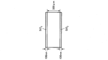
- FIG. 3 is a view for explaining a semiconductor substrate measured by the measuring apparatus of the present embodiment.
- FIG. 4 is a diagram showing the measurement result of the effective carrier lifetime by the measuring apparatus of the present embodiment.
- FIG. 5A is a diagram showing the measurement result of the carrier volume concentration by the measuring apparatus of the present embodiment.
- FIG. 5B is a diagram showing the measurement result of the carrier volume concentration by the measuring apparatus of the present embodiment.
- At least two types of light having different absorption coefficients are irradiated onto a semiconductor substrate that is a sample to be measured.
- the semiconductor substrate when short-wavelength light having a large absorption coefficient is irradiated to the semiconductor substrate, the light is absorbed in the extreme surface region of the semiconductor substrate.
- the surface recombination velocity of the semiconductor substrate is high, the photo-induced carriers generated in the surface region of the semiconductor substrate are rapidly recombined and disappear, so that the concentration of carriers existing in the substrate is small. Therefore, when the semiconductor substrate is irradiated with microwaves, the absorbance of microwaves is small (transmittance is large), and the effective carrier lifetime is small.
- the semiconductor substrate when the semiconductor substrate is irradiated with light having a long wavelength having a small absorption coefficient, the light enters deep inside the semiconductor substrate. For this reason, the influence of the surface recombination rate is reduced, and when the bulk carrier lifetime of the semiconductor substrate is sufficiently large, the carrier concentration becomes larger than that when short wavelength light is irradiated, and the effective carrier lifetime is increased.
- the measured effective carrier lifetime when the effective carrier lifetime is limited by the surface recombination rate (when the surface recombination rate is high), the measured effective carrier lifetime has wavelength dependence, and is irradiated with short-wavelength light.
- the effective carrier lifetime measured from the microwave transmittance detected at 1 and the effective carrier lifetime measured from the microwave transmittance detected when irradiated with light having a long wavelength are different values.
- the photo-induced carriers are the same throughout the semiconductor substrate. Since it disappears at a rate, the measured effective carrier lifetime has no wavelength dependence.
- the surface of the semiconductor substrate is analyzed by analyzing the measured at least two effective carrier lifetimes. Evaluation of recombination velocity and bulk carrier lifetime is possible.
- FIG. 1 is a diagram illustrating an example of a configuration of a measurement apparatus (photo-induced carrier lifetime measurement apparatus) according to the present embodiment.
- the measuring apparatus 1 of the present embodiment measures the effective carrier lifetime of the semiconductor substrate S, which is the sample to be measured, and analyzes the measured effective carrier lifetime to determine the bulk carrier lifetime and surface recombination velocity of the semiconductor substrate S. It is configured as a device that performs measurement.
- the measurement apparatus 1 includes a microwave generation unit 10 that generates a microwave incident on a semiconductor substrate S, and light sources 20 and 22 (light irradiation) that irradiate light (induced light) for generating photoinduced carriers in the semiconductor substrate S. Part), a detection part 30 for detecting the intensity of the microwave transmitted through the semiconductor substrate S, a waveguide 40 for propagating the microwave generated by the microwave generation part 10 to the detection part 30, and a calculation part 50 Including.
- the waveguide 40 is provided with a gap 42 into which the semiconductor substrate S is inserted.
- a reflector 24 for allowing light from the light sources 20 and 22 to enter the semiconductor substrate S is provided on the microwave generation unit 10 side of the gap 42 in the waveguide 40.
- Light from the light sources 20 and 22 passes through the optical fiber 26, is diffusely reflected by the reflector 24, and enters the semiconductor substrate S.
- the reflection plate 24 is made of, for example, a Teflon (registered trademark) plate.
- the light sources 20 and 22 are each composed of, for example, a laser light source, and generate light having different wavelengths (light having different absorption coefficients for the semiconductor substrate S).
- the light source 20 is a light source for irradiating the semiconductor substrate S with short-wavelength light (for example, light that generates carriers in the surface region of the semiconductor substrate S), and the light source 22 is a long-wavelength light ( For example, it is a light source for irradiating the inner region of the semiconductor substrate S with light that generates carriers.
- the calculation unit 50 calculates the effective carrier lifetime of the photoinduced carrier of the semiconductor substrate S based on the intensity information of the microwave detected by the detection unit 30, and the semiconductor substrate based on the calculated effective carrier lifetime. An arithmetic process for calculating the bulk carrier lifetime of S and the surface recombination velocity is performed.
- the calculation unit 50 obtains a change in the microwave transmittance from the microwave intensity information detected when the semiconductor substrate S is irradiated with light having a short wavelength from the light source 20, and based on the obtained change in the transmittance, The effective carrier lifetime (corresponding to the wavelength of the light from the light source 20) when the light from the light source 20 is irradiated onto the semiconductor substrate S is calculated.
- the calculation unit 50 obtains a change in the transmittance of the microwave from the intensity information of the microwave detected when the semiconductor substrate S is irradiated with light having a long wavelength from the light source 22, and determines the change in the obtained transmittance. Based on this, an effective carrier lifetime (corresponding to the wavelength of light from the light source 22) when the semiconductor substrate S is irradiated with light from the light source 22 is calculated.
- the calculation unit 50 uses the two measured effective carrier lifetimes ⁇ eff (the measured value of the effective carrier lifetime when the semiconductor substrate S is irradiated with the light from the light source 20 and the light from the light source 22 as the semiconductor substrate S).
- the bulk carrier lifetime ⁇ b that most closely matches the measured value of the effective carrier lifetime when the light is irradiated to the surface, and the surface recombination velocity (surface recombination velocity S top on the surface irradiated with the induced light (irradiated surface))
- the surface recombination velocity S rear on the side opposite to the irradiated surface side is analyzed and obtained. Note that the analysis of the bulk carrier lifetime ⁇ b and the surface recombination velocities S top and S rear is performed in consideration of the ingress length of the photo carrier.
- the steady light-induced minority carrier volume concentration n (x) at a depth x from the surface (irradiated surface) is expressed as follows: D is the diffusion coefficient of minority carriers in the semiconductor substrate. According to the following differential equation:
- G (x) is a minority carrier generation rate per unit area at a depth x.
- G (x) depends on the light absorption coefficient ⁇ of the semiconductor substrate, and the light absorption coefficient ⁇ depends on the light wavelength.
- FIG. 2 illustrates the change of the light absorption coefficient of crystalline silicon (an example of a semiconductor substrate) with the light wavelength.
- crystalline silicon exhibits a very large absorption coefficient for ultraviolet rays. Therefore, ultraviolet rays are absorbed at the extreme surface of crystalline silicon.
- the absorption coefficient is small for infrared rays close to the band gap. Therefore, infrared rays penetrate deep into the crystalline silicon semiconductor.
- the light intensity J (x) per unit volume at the depth x when the semiconductor substrate surface is irradiated with light of intensity I 0 per unit area can be expressed by the following equation using the light absorption coefficient ⁇ . it can.
- J 0 is I 0 / ⁇ , and is the light volume intensity at the surface of the semiconductor substrate.
- G (x) is proportional to J (x), and as the light intensity increases, G (x) increases and more carriers are generated.
- G (x) is expressed as follows using J (x), photon energy h ⁇ corresponding to the wavelength (h is Planck's constant, ⁇ is the optical frequency), and carrier generation internal quantum efficiency ⁇ . Can do.
- the surface recombination velocities S top and S rear due to the defects existing on the surface of the semiconductor substrate are given as boundary conditions of the differential coefficient on the surface of the semiconductor substrate as in the following equation.
- d is the thickness of the semiconductor substrate.
- the carrier volume concentration n (x) can be obtained by solving the equation (1) using G (x) corresponding to the wavelength using the equations (4) and (5) as boundary conditions.
- the carrier surface density N (unit: cm ⁇ 2 ) obtained by integrating n (x) in the depth direction of the semiconductor substrate and the carrier generation rate per unit area obtained by integrating G (x) in the depth direction of the semiconductor substrate.
- H (unit: cm ⁇ 2 s ⁇ 1 ) is given by the following equation.
- equations (1) to (5) are programmed by the finite element difference method, n (x) is obtained using ⁇ b , S top and S rear as parameters, and N is obtained by integrating the obtained n (x). . Further, G (x) is integrated to obtain H, and the calculated value of effective carrier lifetime ⁇ eff is obtained by substituting the obtained N and H into equation (8).
- ⁇ eff is given by the following equation.
- the calculated value of ⁇ eff calculated for each wavelength of the irradiated light and the measured value of ⁇ eff measured for each wavelength of the irradiated light are the values of the parameters ⁇ b , S top, and S rear . compared with varying, determining the value of tau b, S top and S rear when the calculated value of tau eff is best matches the measured value of tau eff.
- the calculated value of ⁇ eff calculated based on the wavelength of the light from the light source 20 and the measured value of ⁇ eff when the light from the light source 20 is irradiated while changing the parameter value Comparing and comparing the calculated value of ⁇ eff calculated based on the wavelength of light of the light source 22 and the measured value of ⁇ eff when the light from the light source 22 is irradiated while changing the parameter value, Find the most probable ⁇ b , S top and S rear .
- ⁇ b in the equation (1) becomes the bulk carrier lifetime ⁇ b (x) at the depth x from the surface
- the depth distribution of the bulk carrier time by the numerical analysis developed from the above finite element method. (Bulk carrier lifetime ⁇ b for each depth x) can be obtained.
- the thickness d of the semiconductor substrate is divided into M (M is a positive integer) layers, and the differential equation of equation (1) is changed to a difference equation for the thickness d / M of each layer.
- the boundary conditions of Formula (4) and Formula (5) are provided in the front surface and the back surface.
- nM carrier volume concentration of Mth layer
- nM-1 carrier volume concentration of M-1th layer
- .. N1 carrier volume concentration of the first layer
- Equation (8) the measured value of ⁇ eff can be obtained with high accuracy if the carrier surface density N and the carrier generation rate H are known.
- H depends on the photon flux F of incident light, the carrier generation internal quantum efficiency ⁇ , and the light reflection loss R as shown in the following equation.
- the method of measuring ⁇ eff by the periodic pulse method disclosed in Patent Document 1 was applied.
- the periodic pulse method it is possible to measure ⁇ eff by weak light irradiation at the same level as continuous light irradiation.
- the periodic pulse method is not suitable for measuring very small ⁇ eff of less than 10 ⁇ m. Therefore, a method for measuring ⁇ eff was developed using a reference sample similar to the sample to be measured.
- the sample to be measured is crystalline silicon
- a silicon single crystal is used as a reference sample.
- a passivation film such as a thermal oxide film is formed on the surface of the reference sample so that a large ⁇ eff can be obtained while suppressing carrier recombination defects on the surface.
- the thermal oxide film of the reference sample is set to the same thickness as the oxide film of the sample to be measured.
- a thin oxide film for example, a thermal oxide film having a thickness of 10 nm
- the same texture is formed on the reference sample.
- ⁇ eff of the reference sample is obtained by a periodic pulse method. Since ⁇ eff generally varies depending on the light intensity, the average light intensity of the periodic pulse method is set to be the same as the light intensity of continuous light described later.
- the reference sample is irradiated with continuous light and microwave absorption measurement is performed to determine the carrier surface density N of the reference sample. Then, the measured values of N and ⁇ eff are substituted into equation (8) to determine the carrier generation rate H in continuous light irradiation.
- the sample to be measured is irradiated with continuous light and microwave absorption measurement is performed to determine the carrier surface density N of the sample to be measured. Then, the measured values of the carrier surface density N and the carrier generation rate H of the sample to be measured are substituted into the equation (8) to obtain ⁇ eff of the sample to be measured.
- ⁇ eff of the sample to be measured can be accurately measured using accurate H.
- a 500 ⁇ m thick n-type silicon substrate coated on both sides with a 100 nm thick thermal oxide film was used as the first sample.
- a laser beam having a wavelength 940nm of 5 ⁇ 10 4 W / cm 2 strength in the process of irradiating the entire surface (heat treatment) to a second one was carried out Used as a sample. It has been clarified in the prior literature that the effective carrier lifetime is reduced by the heat treatment using such laser irradiation.
- an oscillator that oscillates a 9.35 GHz microwave was used as the microwave generator 10. Further, a laser light source having a wavelength of 635 nm was used as the short wavelength light source 20, and a laser light source having a wavelength of 980 nm was used as the long wavelength light source 22. Light having a wavelength of 635 nm has a small penetration length of 2.7 ⁇ m into silicon and is absorbed by the extreme surface region of the silicon substrate. Light having a wavelength of 980 nm has a large penetration length of 90 ⁇ m and penetrates into the inner region of the silicon substrate. I know that.
- FIG. 4 shows the measurement results of measuring the effective carrier lifetime when irradiating light with a wavelength of 635 nm and the effective carrier lifetime when irradiating light with a wavelength of 980 nm for each of the first sample and the second sample. It is.
- a white dot in the figure is a measurement result when light having a wavelength of 980 nm is irradiated, and a black dot in the figure is a measurement result when light having a wavelength of 635 nm is irradiated.
- the n-type silicon substrate (first sample) coated with the thermal oxide film has an effective carrier lifetime as high as 2 ms, almost the same lifetime value at both wavelengths of 635 nm and 980 nm. became.
- the n-type silicon substrate (second sample) that has been subjected to the heat treatment by laser irradiation has an effective carrier lifetime of 5 ⁇ s when irradiated with light of a wavelength of 635 nm, and is effective when irradiated with light of a wavelength of 980 nm.
- the carrier lifetime was 35 ⁇ s.
- the heat treatment by laser irradiation reduces the effective carrier lifetime and increases the effective carrier lifetime at the time of irradiation with light of a short wavelength as compared with that at the time of irradiation of light of a short wavelength.
- the two effective carrier lifetime measurements measured for the first sample by the analysis method described above are compared with the calculated effective carrier lifetime values calculated at both wavelengths of 635 nm and 980 nm, respectively.
- the bulk carrier lifetime ⁇ b and the surface recombination velocities S top and S rear that best match the two effective carrier lifetime measurements were determined.
- the bulk carrier lifetime ⁇ b was 20 ms
- the surface recombination velocities S top and S rear of the first sample were 12.3 cm / s, respectively.
- the bulk carrier lifetime ⁇ b and the surface recombination velocities S top and S rear that best match the two effective carrier lifetime values measured for the second sample were determined by the analysis method described above. As a result, it was found that the surface recombination speed S top of the irradiated surface of the second sample was 25000 cm / s, and the surface recombination speed of the irradiated surface was increased by the heat treatment by laser irradiation.
- FIG. 5A and 5B show the depth x distribution of the carrier volume concentration n (x) obtained from the analysis result of the second sample.
- FIG. 5A shows a distribution during irradiation with light having a wavelength of 635 nm
- FIG. 5B shows a distribution during irradiation with light having a wavelength of 980 nm.
- both the bulk carrier lifetime and the surface recombination velocity of the semiconductor substrate can be measured without assuming one of them.
- Second Example a 700 ⁇ m thick silicon substrate provided with a thermal oxide film was used as a sample. Silicon atoms were ion-implanted (injection amount: 1 ⁇ 10 14 cm ⁇ 2 ) into this silicon substrate at 70 keV. With respect to this sample, the effective carrier lifetime ⁇ eff before and after ion implantation was measured by light irradiation with a wavelength of 635 nm and a wavelength of 980 nm. Then, the measurement result was analyzed by a finite element method to obtain the surface recombination velocities S top and S rear and the bulk carrier lifetime depth distribution ⁇ b (x). Regarding the bulk carrier lifetime, the thickness of the substrate was divided into a plurality of layers, and ⁇ b was determined for each layer. The measurement results and analysis results are shown in Table 1.
- the first layer is a layer having a depth x from the surface of 0 to 490 ⁇ m
- the second layer is a layer having a depth x from the surface of 490 to 700 ⁇ m.
- ⁇ eff was greatly reduced, and in particular, ⁇ eff during light irradiation with a wavelength of 980 nm was small. This indicates that ⁇ b is lowered deeply on the silicon surface side. As a result of analyzing this measured value, it was found that ⁇ b decreased to 10 ⁇ s over 490 ⁇ m from the surface. Since the depth at which silicon atoms are implanted by ion implantation is about 0.1 ⁇ m at most, carrier recombination defect formation by high-energy ions can be achieved by this measurement up to a deeper portion than the depth at which ions are implanted. It became clear that it was reaching.
- a 500 ⁇ m thick n-type silicon substrate provided with a 100 nm thick thermal oxide film was used as a sample.
- the silicon substrate was irradiated with argon plasma having an output of 50 w for 1 minute.
- the effective carrier lifetime ⁇ eff before and after the plasma treatment was measured by light irradiation with a wavelength of 635 nm and a wavelength of 980 nm.
- the measurement result was analyzed by the finite element method to obtain the surface recombination velocities S top and S rear and the bulk carrier lifetime ⁇ b .
- the measurement results and analysis results are shown in Table 2.
- the present invention is not limited to the above-described embodiment, and various modifications can be made.
- the present invention includes configurations that are substantially the same as the configurations described in the embodiments (for example, configurations that have the same functions, methods, and results, or configurations that have the same objects and effects).
- the invention includes a configuration in which a non-essential part of the configuration described in the embodiment is replaced.
- the present invention includes a configuration that exhibits the same operational effects as the configuration described in the embodiment or a configuration that can achieve the same object.
- the invention includes a configuration in which a known technique is added to the configuration described in the embodiment.
- the measuring apparatus 1 in FIG. 1 includes an X-axis moving stage that moves the semiconductor substrate S in the X-axis direction in FIG. 1 and a Y-axis moving stage that moves the semiconductor substrate S in the Y-axis direction in FIG. May be. If comprised in this way, it will become possible to measure about arbitrary positions on the XY plane in the semiconductor substrate S. Further, the measuring apparatus 1 may be configured so that light from the light sources 20 and 22 is pulse-modulated to detect lock-in of the microwave intensity. The measuring apparatus 1 may also include two or more light sources that emit light having different wavelengths to generate photoinduced carriers.
- microwave generation unit 20 light source, 22 light source, 24 reflector, 26 optical fiber, 30 detection unit, 40 waveguide, 42 gap, 50 calculation unit
Landscapes
- Physics & Mathematics (AREA)
- General Physics & Mathematics (AREA)
- Chemical & Material Sciences (AREA)
- Health & Medical Sciences (AREA)
- Life Sciences & Earth Sciences (AREA)
- Immunology (AREA)
- Biochemistry (AREA)
- General Health & Medical Sciences (AREA)
- Analytical Chemistry (AREA)
- Pathology (AREA)
- Electromagnetism (AREA)
- Nuclear Medicine, Radiotherapy & Molecular Imaging (AREA)
- Chemical Kinetics & Catalysis (AREA)
- Electrochemistry (AREA)
- Engineering & Computer Science (AREA)
- Food Science & Technology (AREA)
- Medicinal Chemistry (AREA)
- Testing Or Measuring Of Semiconductors Or The Like (AREA)
Priority Applications (2)
| Application Number | Priority Date | Filing Date | Title |
|---|---|---|---|
| US14/364,997 US10126253B2 (en) | 2011-12-16 | 2012-12-11 | Photoinduced carrier lifetime measurement device and photoinduced carrier lifetime measurement method |
| CN201280062241.8A CN104094389B (zh) | 2011-12-16 | 2012-12-11 | 光致载流子寿命测量装置及光致载流子寿命测量方法 |
Applications Claiming Priority (4)
| Application Number | Priority Date | Filing Date | Title |
|---|---|---|---|
| JP2011276215 | 2011-12-16 | ||
| JP2011-276215 | 2011-12-16 | ||
| JP2012253129A JP6052536B2 (ja) | 2011-12-16 | 2012-11-19 | 光誘起キャリヤライフタイム測定装置及び光誘起キャリヤライフタイム測定方法 |
| JP2012-253129 | 2012-11-19 |
Publications (1)
| Publication Number | Publication Date |
|---|---|
| WO2013089088A1 true WO2013089088A1 (ja) | 2013-06-20 |
Family
ID=48612535
Family Applications (1)
| Application Number | Title | Priority Date | Filing Date |
|---|---|---|---|
| PCT/JP2012/082038 Ceased WO2013089088A1 (ja) | 2011-12-16 | 2012-12-11 | 光誘起キャリヤライフタイム測定装置及び光誘起キャリヤライフタイム測定方法 |
Country Status (4)
| Country | Link |
|---|---|
| US (1) | US10126253B2 (https=) |
| JP (1) | JP6052536B2 (https=) |
| CN (1) | CN104094389B (https=) |
| WO (1) | WO2013089088A1 (https=) |
Families Citing this family (10)
| Publication number | Priority date | Publication date | Assignee | Title |
|---|---|---|---|---|
| JP2016157931A (ja) * | 2015-02-20 | 2016-09-01 | 国立大学法人東京農工大学 | 光誘起キャリヤライフタイム測定方法及び光誘起キャリヤライフタイム測定装置 |
| JP6382747B2 (ja) * | 2015-02-26 | 2018-08-29 | 京セラ株式会社 | 過剰少数キャリアの実効ライフタイム測定方法および過剰少数キャリアの実効ライフタイム測定装置 |
| JP6826007B2 (ja) * | 2017-06-29 | 2021-02-03 | 京セラ株式会社 | 光誘起キャリアのバルクキャリアライフタイムの測定方法および測定装置 |
| CN107591340A (zh) * | 2017-08-01 | 2018-01-16 | 惠科股份有限公司 | 一种半导体的测试方法和测试装置 |
| CN110470965B (zh) * | 2019-07-09 | 2020-07-28 | 同济大学 | 一种半导体表面态载流子寿命测试方法 |
| CN111128783B (zh) * | 2019-12-30 | 2024-07-16 | 南方科技大学 | 一种少数载流子寿命的纵向分布测试系统和方法 |
| FR3118283B1 (fr) * | 2020-12-18 | 2023-11-24 | Commissariat Energie Atomique | Procédé de détermination de la durée de vie volumique des porteurs de charge d'un substrat et dispositif associé |
| JP7249395B1 (ja) | 2021-11-10 | 2023-03-30 | 株式会社Sumco | 半導体試料の評価方法、半導体試料の評価装置および半導体ウェーハの製造方法 |
| JP7713198B2 (ja) * | 2022-09-20 | 2025-07-25 | 株式会社Sumco | 半導体試料の評価方法 |
| EP4672307A1 (en) * | 2023-02-24 | 2025-12-31 | Sumco Corporation | METHOD AND DEVICE FOR EVALUATING SEMICONDUCTOR SAMPLES AND METHOD FOR MANUFACTURING SEMICONDUCTOR SLICES |
Citations (2)
| Publication number | Priority date | Publication date | Assignee | Title |
|---|---|---|---|---|
| JP2005277417A (ja) * | 2004-03-22 | 2005-10-06 | Kla Tencor Technologies Corp | 試料の1つ又は複数の特性を決定するための方法とシステム |
| JP2011082312A (ja) * | 2009-10-06 | 2011-04-21 | Kobe Steel Ltd | 半導体キャリア寿命測定装置および該方法 |
Family Cites Families (8)
| Publication number | Priority date | Publication date | Assignee | Title |
|---|---|---|---|---|
| US5177351A (en) * | 1988-08-23 | 1993-01-05 | Lagowski Jacek J | Method and apparatus for determining the minority carrier diffusion length from linear constant photon flux photovoltage measurements |
| JPH067564B2 (ja) * | 1988-09-07 | 1994-01-26 | 三菱マテリアル株式会社 | ウェーハ表面の半導体特性測定方法 |
| JP2889307B2 (ja) * | 1990-03-26 | 1999-05-10 | 株式会社東芝 | ▲iv▼族半導体のキャリアライフタイム測定法 |
| JP4441381B2 (ja) * | 2004-10-29 | 2010-03-31 | 三菱電機株式会社 | 表面キャリア再結合速度の測定方法 |
| KR101322591B1 (ko) * | 2009-10-06 | 2013-10-28 | 가부시키가이샤 코베루코 카겐 | 반도체 캐리어 수명 측정 장치 및 그 방법 |
| US9239299B2 (en) * | 2010-02-15 | 2016-01-19 | National University Corporation Tokyo University Of Agriculture And Technology | Photoinduced carrier lifetime measuring method, light incidence efficiency measuring method, photoinduced carrier lifetime measuring device, and light incidence efficiency measuring device |
| US8912799B2 (en) * | 2011-11-10 | 2014-12-16 | Semiconductor Physics Laboratory Co., Ltd. | Accurate measurement of excess carrier lifetime using carrier decay method |
| US9131170B2 (en) * | 2012-04-13 | 2015-09-08 | Andreas Mandelis | Method and apparatus for performing heterodyne lock-in imaging and quantitative non-contact measurements of electrical properties |
-
2012
- 2012-11-19 JP JP2012253129A patent/JP6052536B2/ja active Active
- 2012-12-11 WO PCT/JP2012/082038 patent/WO2013089088A1/ja not_active Ceased
- 2012-12-11 CN CN201280062241.8A patent/CN104094389B/zh not_active Expired - Fee Related
- 2012-12-11 US US14/364,997 patent/US10126253B2/en not_active Expired - Fee Related
Patent Citations (2)
| Publication number | Priority date | Publication date | Assignee | Title |
|---|---|---|---|---|
| JP2005277417A (ja) * | 2004-03-22 | 2005-10-06 | Kla Tencor Technologies Corp | 試料の1つ又は複数の特性を決定するための方法とシステム |
| JP2011082312A (ja) * | 2009-10-06 | 2011-04-21 | Kobe Steel Ltd | 半導体キャリア寿命測定装置および該方法 |
Also Published As
| Publication number | Publication date |
|---|---|
| CN104094389B (zh) | 2016-09-07 |
| US20140303919A1 (en) | 2014-10-09 |
| JP2013145868A (ja) | 2013-07-25 |
| US10126253B2 (en) | 2018-11-13 |
| JP6052536B2 (ja) | 2016-12-27 |
| CN104094389A (zh) | 2014-10-08 |
Similar Documents
| Publication | Publication Date | Title |
|---|---|---|
| JP6052536B2 (ja) | 光誘起キャリヤライフタイム測定装置及び光誘起キャリヤライフタイム測定方法 | |
| TWI451080B (zh) | Method for evaluating crystallinity of thin film semiconductor and method thereof | |
| JP5105903B2 (ja) | レーザアニール装置及びアニール方法 | |
| JP5295924B2 (ja) | 半導体キャリア寿命測定装置および該方法 | |
| JPH0272646A (ja) | ウェーハ表面の半導体特性測定方法 | |
| KR101322591B1 (ko) | 반도체 캐리어 수명 측정 장치 및 그 방법 | |
| KR940010642B1 (ko) | 반도체 기판표면의 전자적 상태의 평가방법 및 그 장치 | |
| US9239299B2 (en) | Photoinduced carrier lifetime measuring method, light incidence efficiency measuring method, photoinduced carrier lifetime measuring device, and light incidence efficiency measuring device | |
| JP2019012740A (ja) | 光誘起キャリアのバルクキャリアライフタイムの測定方法および測定装置 | |
| RU2450387C1 (ru) | Способ бесконтактного определения времени жизни неравновесных носителей заряда в полупроводниках | |
| JP5858833B2 (ja) | 半導体評価方法、及び半導体評価装置 | |
| JP5818364B2 (ja) | 半導体基板と絶縁膜との界面評価方法、及び半導体基板と絶縁膜との界面評価装置 | |
| JP6382747B2 (ja) | 過剰少数キャリアの実効ライフタイム測定方法および過剰少数キャリアの実効ライフタイム測定装置 | |
| JP2016157931A (ja) | 光誘起キャリヤライフタイム測定方法及び光誘起キャリヤライフタイム測定装置 | |
| CN110196240B (zh) | 基于pl干涉现象的激光改性测量薄膜折射率和厚度的方法 | |
| JPS6253944B2 (https=) | ||
| CN113740265A (zh) | 多元素材料AnBxC1-x元素配比的检测方法 | |
| CN114414041A (zh) | 具有皮秒量级的可见光和射线脉冲探测方法及固体条纹相机 | |
| JP2017212329A (ja) | キャリアライフタイム測定装置およびキャリアライフタイムの測定方法 | |
| Bobretsova et al. | Optical absorption in a waveguide based on an n-type AlGaAs heterostructure | |
| Vreugdenhil | Electron-induced carrier dynamics in semiconductors | |
| JPH04289442A (ja) | ライフタイム測定方法 | |
| Sameshima et al. | Minority carrier lifetime measurements by multiple wavelength light induced carrier microwave absorption method | |
| Zinovchuk et al. | Measurement of surface recombination velocity and bulk lifetime in Si wafers by the kinetics of excess thermal emission | |
| Knabe | Spectral photoluminescence for the characterization of excitation states in semiconductors and fluorescence solar collectors with manipulation of the in and out coupling of radiation |
Legal Events
| Date | Code | Title | Description |
|---|---|---|---|
| 121 | Ep: the epo has been informed by wipo that ep was designated in this application |
Ref document number: 12858545 Country of ref document: EP Kind code of ref document: A1 |
|
| DPE2 | Request for preliminary examination filed before expiration of 19th month from priority date (pct application filed from 20040101) | ||
| WWE | Wipo information: entry into national phase |
Ref document number: 14364997 Country of ref document: US |
|
| NENP | Non-entry into the national phase |
Ref country code: DE |
|
| 122 | Ep: pct application non-entry in european phase |
Ref document number: 12858545 Country of ref document: EP Kind code of ref document: A1 |