WO2013084809A1 - 撮像素子、制御方法、並びに、撮像装置 - Google Patents
撮像素子、制御方法、並びに、撮像装置 Download PDFInfo
- Publication number
- WO2013084809A1 WO2013084809A1 PCT/JP2012/081053 JP2012081053W WO2013084809A1 WO 2013084809 A1 WO2013084809 A1 WO 2013084809A1 JP 2012081053 W JP2012081053 W JP 2012081053W WO 2013084809 A1 WO2013084809 A1 WO 2013084809A1
- Authority
- WO
- WIPO (PCT)
- Prior art keywords
- reference signal
- comparison
- signal
- unit
- output
- Prior art date
- Legal status (The legal status is an assumption and is not a legal conclusion. Google has not performed a legal analysis and makes no representation as to the accuracy of the status listed.)
- Ceased
Links
Images







Classifications
-
- H—ELECTRICITY
- H03—ELECTRONIC CIRCUITRY
- H03M—CODING; DECODING; CODE CONVERSION IN GENERAL
- H03M1/00—Analogue/digital conversion; Digital/analogue conversion
- H03M1/12—Analogue/digital converters
- H03M1/18—Automatic control for modifying the range of signals the converter can handle, e.g. gain ranging
- H03M1/188—Multi-path, i.e. having a separate analogue/digital converter for each possible range
-
- H—ELECTRICITY
- H04—ELECTRIC COMMUNICATION TECHNIQUE
- H04N—PICTORIAL COMMUNICATION, e.g. TELEVISION
- H04N25/00—Circuitry of solid-state image sensors [SSIS]; Control thereof
- H04N25/70—SSIS architectures; Circuits associated therewith
- H04N25/76—Addressed sensors, e.g. MOS or CMOS sensors
- H04N25/77—Pixel circuitry, e.g. memories, A/D converters, pixel amplifiers, shared circuits or shared components
-
- H—ELECTRICITY
- H04—ELECTRIC COMMUNICATION TECHNIQUE
- H04N—PICTORIAL COMMUNICATION, e.g. TELEVISION
- H04N25/00—Circuitry of solid-state image sensors [SSIS]; Control thereof
- H04N25/70—SSIS architectures; Circuits associated therewith
- H04N25/76—Addressed sensors, e.g. MOS or CMOS sensors
- H04N25/7795—Circuitry for generating timing or clock signals
-
- H—ELECTRICITY
- H04—ELECTRIC COMMUNICATION TECHNIQUE
- H04N—PICTORIAL COMMUNICATION, e.g. TELEVISION
- H04N25/00—Circuitry of solid-state image sensors [SSIS]; Control thereof
- H04N25/70—SSIS architectures; Circuits associated therewith
- H04N25/76—Addressed sensors, e.g. MOS or CMOS sensors
- H04N25/78—Readout circuits for addressed sensors, e.g. output amplifiers or A/D converters
-
- H—ELECTRICITY
- H03—ELECTRONIC CIRCUITRY
- H03M—CODING; DECODING; CODE CONVERSION IN GENERAL
- H03M1/00—Analogue/digital conversion; Digital/analogue conversion
- H03M1/12—Analogue/digital converters
- H03M1/1205—Multiplexed conversion systems
- H03M1/123—Simultaneous, i.e. using one converter per channel but with common control or reference circuits for multiple converters
-
- H—ELECTRICITY
- H03—ELECTRONIC CIRCUITRY
- H03M—CODING; DECODING; CODE CONVERSION IN GENERAL
- H03M1/00—Analogue/digital conversion; Digital/analogue conversion
- H03M1/12—Analogue/digital converters
- H03M1/124—Sampling or signal conditioning arrangements specially adapted for A/D converters
-
- H—ELECTRICITY
- H03—ELECTRONIC CIRCUITRY
- H03M—CODING; DECODING; CODE CONVERSION IN GENERAL
- H03M1/00—Analogue/digital conversion; Digital/analogue conversion
- H03M1/12—Analogue/digital converters
- H03M1/50—Analogue/digital converters with intermediate conversion to time interval
- H03M1/56—Input signal compared with linear ramp
-
- H—ELECTRICITY
- H04—ELECTRIC COMMUNICATION TECHNIQUE
- H04N—PICTORIAL COMMUNICATION, e.g. TELEVISION
- H04N25/00—Circuitry of solid-state image sensors [SSIS]; Control thereof
- H04N25/50—Control of the SSIS exposure
- H04N25/57—Control of the dynamic range
-
- H—ELECTRICITY
- H04—ELECTRIC COMMUNICATION TECHNIQUE
- H04N—PICTORIAL COMMUNICATION, e.g. TELEVISION
- H04N25/00—Circuitry of solid-state image sensors [SSIS]; Control thereof
- H04N25/60—Noise processing, e.g. detecting, correcting, reducing or removing noise
- H04N25/65—Noise processing, e.g. detecting, correcting, reducing or removing noise applied to reset noise, e.g. KTC noise related to CMOS structures by techniques other than CDS
Definitions
- the present disclosure relates to an imaging element, a control method, and an imaging apparatus, and particularly relates to an imaging element, a control method, and an imaging apparatus that can obtain a higher quality image.
- a / D (Analog / Digital) conversion operations in CMOS (Complementary Metal Oxide Semiconductor) image sensors time-integrating A / D converters using a ramp waveform as a reference voltage are widely used.
- a time-integrating A / D converter has good linearity and noise characteristics.
- a reference voltage generator can be shared between A / D converters for each column. Therefore, the area and power efficiency are good, and the compatibility with the CMOS image sensor is good compared with other A / D conversion methods.
- the output gradient is set by dividing the input into the image sensor (light intensity) into multiple sections.
- a method of simultaneously operating a plurality of linear A / D converters in parallel was also considered.
- This disclosure has been made in view of such a situation, and aims to obtain a higher quality image.
- One aspect of the present disclosure includes a plurality of comparison units that compare an analog signal supplied from a pixel including a photoelectric conversion element via a vertical signal line with reference signals of ramp waves having different inclinations and output a comparison result.
- a plurality of counters that count until the comparison result is inverted for the different comparison units, and output the count value as digital data; a reference signal of a ramp wave other than the analog signal and the ramp wave having the slowest slope
- the comparison unit that performs comparison with the analog signal holds the analog signal supplied through the vertical signal line before starting the comparison, and while the comparison unit performs the comparison, the vertical signal line and the
- the image pickup device includes a sample and hold unit that electrically disconnects the comparison unit and supplies the held analog signal to the comparison unit.
- the voltage range of the ramp wave with the gentlest slope can operate in a range where the kT / C noise is the most dominant of all noises.
- Counting is performed for a comparison unit that compares the analog signal selected from a plurality of the counters based on the comparison result of each comparison unit with a reference signal corresponding to an illuminance region corresponding to the signal level of the analog signal.
- a counter can output the count value.
- the counter having the largest count value and the comparison result of the comparison unit to which it corresponds can be selected.
- the flag information indicating the voltage range of the reference signal used by the comparator corresponding to the selected counter can be output together with the count value.
- the sample hold unit electrically connects or disconnects the vertical signal line and the comparison unit, and electrically connects the vertical signal line and the comparison unit by the switch.
- the analog signal supplied through the vertical signal line is held while the vertical signal line and the comparison unit are electrically disconnected from each other.
- a plurality of the reference signal generation units can start generating the reference signal at the same timing.
- the reference signal generation unit that generates the reference signal of the ramp wave having the gentlest slope After the reference signal generation unit that generates the reference signal of the ramp wave having the gentlest slope generates the reference signal, the slope of the ramp wave and the ramp wave of the other slope do not cross each other at a voltage.
- the reference signal generation unit that generates the reference signal of the ramp wave can start generating the reference signal.
- the reference signal generation unit that generates the reference signal of the ramp wave having the other slope at the timing before the reference signal generation unit that generates the reference signal of the ramp wave having the gentlest slope generates the reference signal, The generation of the reference signal can be started.
- the reference signal generation unit that generates the ramp wave reference signal with the gentlest inclination generates the reference signal
- the reference signal generation units that generate the ramp wave reference signals with other inclinations are inclined with respect to each other. Reference signals of different ramp waves can be sequentially generated.
- a part or all of the plurality of comparison units compare the analog signal with a ramp wave reference signal having the same slope, and compare the analog signal with a ramp wave reference signal having the same slope. It is possible to further include an addition averaging unit that adds and averages the count values output by the counters corresponding to the comparison units.
- One aspect of the present disclosure is also a method for controlling an imaging element, in which a plurality of comparison units convert analog signals supplied from pixels including photoelectric conversion elements via vertical signal lines into ramp waves having different slopes. And a comparison result is output, and a plurality of counters count until the comparison result is inverted for the different comparison units, and output a count value as digital data.
- the comparison unit that compares the analog signal with a reference signal of a ramp wave other than the ramp wave having the slowest slope holds the analog signal supplied through the vertical signal line before starting the comparison. While the comparison unit performs the comparison, the vertical signal line and the comparison unit are electrically disconnected and the held analog signal is supplied to the comparison unit. It is a control method for.
- a plurality of comparisons that further compare an analog signal supplied from a pixel including a photoelectric conversion element via a vertical signal line with a reference signal of a ramp wave having different slopes and output a comparison result. And a plurality of counters that count until the comparison result is inverted for the comparison units that are different from each other, and output a count value as digital data, and the analog signal and the ramp wave other than the ramp wave with the slowest slope.
- the analog signal supplied via the vertical signal line is held, and while the comparison unit performs the comparison, the vertical signal line And an image sensor having a sample-and-hold unit that electrically disconnects the analog signal being held and supplies the analog signal to the comparison unit
- An image processing section performing image processing on the digital data of the captured image output from the imaging device, an imaging apparatus and a storage unit for storing the digital data of the image processed the captured image by the image processing unit.
- Another aspect of the present disclosure provides a plurality of reference signal generation units that generate ramp wave reference signals having different inclinations at different timings, and an analog supplied from a pixel including a photoelectric conversion element via a vertical signal line.
- the signal is compared with the reference signals generated by the different reference signal generation units, and a plurality of comparison units that output comparison results and the comparison units that are different from each other are counted until the comparison result is inverted.
- An imaging device including a plurality of counters that output values as digital data.
- the reference signal generation unit that generates the reference signal of the ramp wave having the gentlest slope After the reference signal generation unit that generates the reference signal of the ramp wave having the gentlest slope generates the reference signal, the slope of the ramp wave and the ramp wave of the other slope do not cross each other at a voltage.
- the reference signal generation unit that generates the reference signal of the ramp wave can start generating the reference signal.
- the reference signal generation unit that generates the reference signal of the ramp wave having the other slope at the timing before the reference signal generation unit that generates the reference signal of the ramp wave having the gentlest slope generates the reference signal, The generation of the reference signal can be started.
- the flag information indicating the voltage range of the reference signal used by the comparator corresponding to the selected counter can be output together with the count value.
- Another aspect of the present disclosure is also a method for controlling an imaging element, in which a plurality of reference signal generation units generate ramp wave reference signals having different inclinations at different timings, and the plurality of comparison units include The analog signal supplied from the pixel including the photoelectric conversion element via the vertical signal line is compared with the reference signal generated by the different reference signal generation units, and a comparison result is output.
- the different comparison units are counted until the comparison result is inverted, and the count value is output as digital data.
- a plurality of reference signal generation units that generate ramp wave reference signals having different inclinations at different timings and pixels including photoelectric conversion elements are supplied via vertical signal lines.
- Analog signals to be compared with the reference signals generated by the different reference signal generation units, and a plurality of comparison units outputting comparison results and the comparison units different from each other are counted until the comparison results are inverted.
- An image sensor having a plurality of counters that output count values as digital data, an image processing unit that performs image processing on digital data of a captured image output from the image sensor, and the image processing unit that performs image processing by the image processing unit
- An imaging apparatus including a storage unit that stores digital data of a captured image.
- an analog signal supplied from a pixel including a photoelectric conversion element via a vertical signal line is compared with a reference signal of a ramp wave having a different slope, a comparison result is output, and a different comparison is performed.
- the comparison unit counts until the comparison result is inverted, the count value is output as digital data, and the comparison unit that compares the analog signal with a reference signal of a ramp wave other than the ramp wave having the slowest slope starts comparison.
- the vertical signal line and the comparison unit are electrically disconnected and held in the analog signal A signal is supplied to the comparator.
- reference signals of ramp waves having different slopes are generated at different timings, and analog signals supplied from pixels including photoelectric conversion elements via vertical signal lines are different from each other.
- the comparison result is output with the reference signal generated by the signal generation unit, the comparison result is counted until the comparison result is inverted for the different comparison units, and the count value is output as digital data.
- the subject can be imaged.
- a higher quality image can be obtained.
- FIG. 10 is a circuit diagram showing another configuration example of the column A / D. It is a block diagram which shows the main structural examples of the imaging device to which this technique is applied. And FIG. 20 is a block diagram illustrating a main configuration example of a computer.
- an A / D converter (also referred to as a column ADC (Analog Digital Converter)) is provided for each pixel column, and a vertical signal line output (pixel value or the like) is A / D converted.
- a column ADC Analog Digital Converter
- the reference voltage generator can be shared by a plurality of A / D converters arranged in this way, so that the area and power efficiency are good. Therefore, it is suitable as an A / D converter (column ADC) for each pixel column.
- Fig. 1 shows one A / D conversion time when the sensor output is increased by 1 bit.
- a certain bit gradation output performs a comparison operation over time T with a ramp reference voltage having a gain of 0 dB of the reference voltage generation circuit.
- To increase the number of output bits by 1 bit operate with a reference voltage gain of 6 dB and reduce the ramp slope of the reference voltage to half, so do full-scale A / D conversion without losing the dynamic range. Then, it takes twice the conversion time 2T.
- a method for increasing the number of output bits without sacrificing the frame rate a method for increasing the count frequency is also effective, but there are limits to the frequencies that can be used in consideration of operation reliability.
- a method of doubling A / D converters and processing in parallel is also conceivable, power consumption and circuit area are doubled.
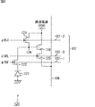
- FIG. 2 is a diagram for explaining an example of how noise is generated by kickback.
- the comparison operation is started simultaneously with a plurality of ramp waves having different inclinations, since the pixel signal levels to be compared are the same, the comparator of the ramp wave having the steep inclination always inverts the output first. As shown in FIG. 2, the output inversion of the comparator is transmitted through the feedback path, and the pixel signal of the pixel vertical signal line may be fluctuated.
- FIG. 3 is a block diagram showing a configuration example of a part of an image sensor to which the present technology is applied.
- a CMOS (Complementary Metal Oxide Semiconductor) image sensor 100 shown in FIG. 3 is an image sensor that captures a subject and obtains digital data of the captured image.
- CMOS Complementary Metal Oxide Semiconductor
- CMOS image sensor 100 a plurality of A / D conversion units that perform A / D conversion using reference signals having different gradations are provided for one vertical signal line, thereby partially preventing the frame rate from being sacrificed. A / D conversion operation with high gradation is realized.
- the CMOS image sensor 100 In the CMOS image sensor 100, during the A / D conversion, the vertical signal line input of the A / D conversion unit that uses the reference signal having the highest gradation is electrically disconnected from other circuits, thereby affecting the influence of kickback. Is suppressed from propagating to other A / D converters. By doing so, the CMOS image sensor 100 can suppress generation of noise due to kickback.
- the CMOS image sensor 100 includes a pixel array unit 102 formed on a semiconductor substrate (hereinafter also referred to as “chip”) 101, and a chip 101 that is the same as the pixel array unit 102. And a peripheral circuit portion integrated thereon.
- a row scanning unit 103, a column processing unit 104, a column scanning unit 105, and a system control unit 106 are provided as peripheral circuit units.
- unit pixels (hereinafter sometimes simply referred to as “pixels”) 120 each having a photoelectric conversion element that generates and accumulates photoelectric charges having a charge amount corresponding to the amount of incident light are arranged in a matrix.
- pixels unit pixels
- each square in the pixel array unit 102 indicates a pixel 120.
- FIG. 3 among the pixels 120 arranged in a matrix, only the pixel 120 at the upper right end is given a reference numeral. However, if there is no need to distinguish between the pixels, any pixel arranged in a matrix Is also referred to as “pixel 120”.
- the pixel array unit 102 is further provided with a pixel drive line 107 for each pixel row with respect to the matrix-like pixel arrangement along the horizontal direction / row direction (pixel arrangement direction of the pixel row), and vertical for each pixel column.
- the signal line 108 is wired along the vertical direction / column direction (pixel arrangement direction of the pixel column).
- the pixel drive line 107 transmits a drive signal for performing driving for reading a signal from the pixel.
- the pixel drive line 107 is illustrated as one wiring, but the number is not limited to one.
- One end of the pixel drive line 107 is connected to an output end corresponding to each row of the row scanning unit 103.
- the row scanning unit 103 includes a shift register, an address decoder, and the like, and is a pixel driving unit that drives each pixel 120 of the pixel array unit 102 at the same time or in units of rows. Although the specific configuration of the row scanning unit 103 is not illustrated, the row scanning unit 103 generally has two scanning systems, a reading scanning system and a sweeping scanning system.
- the readout scanning system selectively scans the unit pixels of the pixel array unit 102 in order in units of rows in order to read out signals from the unit pixels.
- the signal read from the unit pixel is an analog signal.
- the sweep-out scanning system performs sweep-out scanning with respect to the readout row on which readout scanning is performed by the readout scanning system, preceding the readout scanning by a time corresponding to the shutter speed.
- the unnecessary charge is swept out from the photoelectric conversion element of the unit pixel in the readout row by the sweep scanning by the sweep scanning system, so that the photoelectric conversion element is reset.
- a so-called electronic shutter operation is performed by sweeping (reset) unnecessary charges by the sweep scanning system.
- the electronic shutter operation refers to an operation in which the photoelectric charge of the photoelectric conversion element is discarded and a new exposure is started (photocharge accumulation is started).
- the signal read out by the readout operation by the readout scanning system corresponds to the amount of light incident after the immediately preceding readout operation or electronic shutter operation.
- the period from the read timing by the immediately preceding read operation or the sweep timing by the electronic shutter operation to the read timing by the current read operation is the photocharge accumulation period (exposure period) in the unit pixel.
- a signal output from each pixel 120 in the pixel row selectively scanned by the row scanning unit 103 is supplied to the column processing unit 104 through each of the vertical signal lines 108.
- the column processing unit 104 performs predetermined signal processing on a signal output from each pixel 120 of the selected row by the row scanning unit 103 through the vertical signal line 108 for each pixel column of the pixel array unit 102 and performs signal processing.
- the subsequent pixel signal is temporarily held.
- the column processing unit 104 receives the signal of the unit pixel 120, and performs noise removal, signal amplification, A / D conversion, for example, by CDS (Correlated Double Sampling) on the signal. Signal processing.
- CDS Correlated Double Sampling
- the noise removal processing by CDS is performed by, for example, a reset level read when a unit pixel (actually, a floating diffusion section described later) is reset, and a signal level read according to a signal charge photoelectrically converted by a photoelectric conversion element. This is done by taking the difference between By this noise removal processing, pixel-specific fixed pattern noise such as reset noise and variation in threshold values of amplification transistors is removed.
- the signal processing illustrated here is only an example, and the signal processing is not limited to these.
- the column processing unit 104 is provided with a column ADC for each pixel column.
- the above-described A / D conversion for each pixel column is performed by these column ADCs.
- the column processing unit 104 includes a plurality of reference signal generation circuits.
- Each reference signal generation circuit generates a ramp wave as a reference signal. However, the slopes of the ramp waves generated by the respective reference signal generation circuits are different from each other.
- the column ADC has a plurality of A / D conversion units for one vertical signal line.
- the plurality of A / D converters use reference signals generated by different reference signal generation circuits. That is, each A / D converter uses ramp waves having different inclinations. As the slope of the ramp wave becomes gentler, the A / D converter can perform A / D conversion with higher gradation (the number of output bits can be increased). That is, the column ADC can perform A / D conversion with a plurality of types of gradations.
- the column ADC divides the range of values that the vertical signal line output can take into a plurality of areas (illuminance areas), and only a part of the illuminance areas uses a ramp wave with a gentle slope to achieve a high gradation A Perform / D conversion.
- more precise image data is required in a low illuminance region where the pixel output signal is small.
- the column ADC performs A / D conversion with the highest gradation using the ramp wave with the slowest slope only in the preset low-light area, and the slope is steep for the whole. Performs A / D conversion with the least gradation using ramp waves.
- the column ADC of the column processing unit 104 can realize a partially high-gradation A / D conversion operation without sacrificing the frame rate.
- a reference signal generation circuit 131 and a reference signal generation circuit 132 are provided as reference signal generation circuits.
- the reference signal generation circuit 131 generates a reference signal used for high gradation A / D conversion
- the reference signal generation circuit 132 generates a reference signal used for low gradation A / D conversion. That is, the reference signal generation circuit 131 generates a ramp wave having a gentler slope than the reference signal generation circuit 132 as the reference signal.
- Each reference signal (ramp wave) generated by the reference signal generation circuit 131 and the reference signal generation circuit 132 is supplied to an A / D conversion unit corresponding to each column ADC.
- two A / D converters are provided for each vertical signal line.
- One of the A / D converters performs high-gradation A / D conversion using a ramp wave with a gentle slope generated by the reference signal generation circuit 131, and the other A / D converter performs reference.
- Low-gradation A / D conversion is performed using a ramp wave with a steep slope generated by the signal generation circuit 132.
- the column scanning unit 105 includes a shift register, an address decoder, and the like, and sequentially selects unit circuits corresponding to the pixel columns of the column processing unit 104.
- the pixel signals processed by the column processing unit 104 are sequentially output to the horizontal bus 109, supplied to the output terminal (Vout) 110 via the horizontal bus 109, and output thereof.
- the data is transmitted from the terminal 110 to the outside of the semiconductor substrate 101 (CMOS image sensor 100).
- the system control unit 106 receives a clock given from the outside of the semiconductor substrate 101, data for instructing an operation mode, and the like, and outputs data such as internal information of the CMOS image sensor 100.
- the system control unit 106 further includes a timing generator that generates various timing signals.
- the row scanning unit 103 and the column processing unit are directly or indirectly based on the various timing signals generated by the timing generator.
- 104 and drive control of peripheral circuit units such as the column scanning unit 105 are performed.
- the system control unit 106 controls the reference signal generation by the reference signal generation circuit 131 and the reference signal generation circuit 132 of the column processing unit 104. Further, for example, the system control unit 106 controls the operation of each column ADC in the column processing unit 104 by controlling the column scanning unit 105.
- FIG. 4 is a circuit diagram illustrating an example of the circuit configuration of the pixel 120.
- the pixel 120 includes, for example, four transistors such as a transfer transistor 122, a reset transistor 123, an amplification transistor 124, and a selection transistor 125 in addition to, for example, a photodiode 121 that is a photoelectric conversion unit.
- N-channel MOS (Metal Oxide Semiconductor) transistors are used as the four transistors (transfer transistor 122 to selection transistor 125).
- MOS Metal Oxide Semiconductor
- the combination of conductivity types of the transfer transistor 122, the reset transistor 123, the amplification transistor 124, and the selection transistor 125 illustrated here is merely an example, and is not limited to these combinations.
- a pixel drive line 107 for example, three drive wirings of a transfer line 107-1, a reset line 107-2, and a selection line 107-3 are provided in common for each pixel in the same pixel row. ing. One end of each of the transfer line 107-1, the reset line 107-2, and the selection line 107-3 is connected to the output end corresponding to each pixel row of the row scanning unit 103 in units of pixel rows.
- a transfer pulse ⁇ TRF, a reset pulse ⁇ RST, and a selection pulse ⁇ SEL which are drive signals to be driven, are transmitted.
- the photodiode 121 has an anode electrode connected to a negative power source (for example, ground), and photoelectrically converts the received light into a photocharge (here, photoelectrons) having a charge amount corresponding to the amount of light. Accumulate.
- the cathode electrode of the photodiode 121 is electrically connected to the gate electrode of the amplification transistor 124 through the transfer transistor 122.
- a node 126 electrically connected to the gate electrode of the amplification transistor 124 is called an FD (floating diffusion) portion.
- the transfer transistor 122 is connected between the cathode electrode of the photodiode 121 and the FD unit 126.
- a transfer pulse ⁇ TRF with a high level (for example, Vdd level) active (hereinafter referred to as “High active”) is applied to the gate electrode of the transfer transistor 122 via the transfer line 107-1.
- High active a transfer pulse ⁇ TRF with a high level (for example, Vdd level) active
- the reset transistor 123 has a drain electrode connected to the pixel power source Vdd and a source electrode connected to the FD unit 126.
- a high active reset pulse ⁇ RST is applied to the gate electrode of the reset transistor 123 via the reset line 107-2.
- the reset transistor 123 is turned on, and the FD unit 126 is reset by discarding the charge of the FD unit 126 to the pixel power supply Vdd.
- the amplification transistor 124 has a gate electrode connected to the FD unit 126 and a drain electrode connected to the pixel power source Vdd.
- the amplification transistor 124 outputs the potential of the FD unit 126 after being reset by the reset transistor 123 as a reset signal (reset level). Further, the amplification transistor 124 outputs the potential of the FD unit 126 after the transfer of the signal charge by the transfer transistor 122 as an optical accumulation signal (signal level).
- the selection transistor 125 has, for example, a drain electrode connected to the source electrode of the amplification transistor 124 and a source electrode connected to the vertical signal line 108.
- a high active selection pulse ⁇ SEL is applied to the gate electrode of the selection transistor 125 via a selection line 107-3. As a result, the selection transistor 125 is turned on, and the signal output from the amplification transistor 124 is relayed to the vertical signal line 108 with the pixel 120 selected.
- the selection transistor 125 may have a circuit configuration connected between the pixel power supply Vdd and the drain of the amplification transistor 124.
- the pixel 120 is not limited to the pixel configuration including the four transistors having the above configuration.
- a pixel configuration including three transistors that serve as both the amplification transistor 124 and the selection transistor 125 may be used, and the configuration of the pixel circuit is not limited.
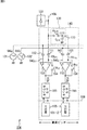
- FIG. 5 is a block diagram illustrating a main configuration example of the column ADC of the column processing unit 104.
- the column ADC 140 shown in FIG. 5 is a configuration example of one vertical signal line segment.
- the column ADC 140 having the configuration shown in FIG. 5 is provided for each vertical signal line.
- the column ADC 140 includes a plurality of A / D conversion units that perform A / D conversion with different gradations.
- the column ADC 140 has two A / D conversions of an A / D conversion unit that performs high gradation A / D conversion and an A / D conversion unit that performs low gradation A / D conversion.
- the left configuration in the column ADC 140 surrounded by a dotted frame is an A / D conversion unit (also referred to as a high gradation A / D conversion unit) that performs high gradation A / D conversion.
- the right configuration is an A / D converter (also referred to as a low gradation A / D converter) that performs low gradation A / D conversion.
- the high gradation A / D conversion unit includes capacitors 151 and 152, a comparator 153, a switch ( ⁇ AZ ) 154, and a U / D counter 155.
- the low gradation A / D conversion unit includes capacitors 161 and 162, a comparator 163, a switch ( ⁇ AZ ) 164, and a U / D counter 165.
- HSCAN 105-1 and HSCAN 105-2 are schematic representations of the functions of the column scanning unit 105 (control signals supplied from the column scanning unit 105) for the respective A / D conversion units. It does not exist in the processing unit 104.
- a signal (vertical signal line output) supplied from the pixel array unit 102 via the vertical signal line 108 is supplied to one input of the comparator 153 via the capacitor 151 (VSL Fi ).
- a reference signal supplied from the reference signal generation circuit 131 that is, a ramp wave with a gentle slope, is supplied to the other input of the comparator 153 via the capacitor 152 (DAC Fi ).
- the comparator 153 compares both inputs and outputs a signal indicating the comparison result (which is greater) (VCO F ).
- the switch 154 appropriately performs analog CDS by connecting the input and output of the comparator 153, and removes the offset of the comparator 153.
- the U / D counter 155 starts counting at a predetermined pace (increment of the count value) along with the start of the comparison by the comparator 153 according to the control of the HSCAN 105-1.
- the U / D counter 155 terminates the count, holds the count value up to that point, and outputs it to the horizontal bus 109 as appropriate under the control of the HSCAN 105-1.
- the high gradation A / D converter performs high gradation A / D conversion in a low illuminance area.
- the vertical signal line output is supplied to one input of the comparator 163 via the capacitor 161 (VSL Ci ).
- the reference signal supplied from the reference signal generation circuit 132 that is, a ramp wave having a steep slope, is supplied to the other input of the comparator 163 via the capacitor 162 (DAC Ci ).
- the comparator 163 compares both inputs and outputs a signal indicating the comparison result (which is greater) (VCO C ).
- the switch 164 performs analog CDS by connecting the input and output of the comparator 163 as appropriate, and removes the offset of the comparator 163.
- the U / D counter 165 starts counting at a predetermined pace (increment of the count value) along with the start of comparison by the comparator 163 according to the control of the HSCAN 105-2.
- the U / D counter 165 ends the count, holds the count value up to that point, and outputs it to the horizontal bus 109 as appropriate under the control of the HSCAN 105-2.
- the low gradation A / D converter performs low gradation A / D conversion of the entire area.
- the column ADC 140 further includes a sample hold unit 170.
- the sample hold unit 170 is provided between the vertical signal line 108 and the capacitor 161.
- the sample hold unit 170 includes a switch ( ⁇ S / H ) 171 and a capacitor (C S / H ) 172.
- the switch 171 electrically connects or disconnects the vertical signal line 108 and the capacitor 161.
- the capacitor 172 holds the vertical signal line output.
- the switch 171 is opened while the low gradation A / D converter performs A / D conversion, and electrically disconnects the vertical signal line 108 and the capacitor 161.
- parasitic capacitance is likely to occur between the input and output due to the circuit configuration, and the inversion of the output affects the input side, and the signal level of the input signal may fluctuate (there is a possibility of kickback). .
- the switch 171 can suppress propagation of the fluctuation by electrically disconnecting the vertical signal line 108 and the capacitor 161 during A / D conversion. That is, the switch 171 can suppress the generation of noise due to kickback.
- the vertical signal line 108 and the capacitor 161 are electrically disconnected, the vertical signal line output is not input to the comparator 163. Therefore, in the switch 171, the vertical signal line 108 and the capacitor 161 are electrically connected while A / D conversion is not performed by the low gradation A / D conversion unit. By doing so, the signal level of the vertical signal line output is accumulated in the capacitor 172. That is, after the switch 171 is cut, the signal level accumulated in the capacitor 172 is supplied to the low gradation A / D converter.
- the sample hold unit 170 can suppress the propagation of signal level fluctuations due to kickback, and can suppress the occurrence of noise due to kickback. Therefore, the column ADC 140 can perform high-gradation A / D conversion partially while suppressing the generation of noise due to kickback without sacrificing the frame rate with a simple configuration. Therefore, the CMOS image sensor 100 can obtain a higher quality image.
- the column ADC 140 configured as described above must be laid out so as to fit within the horizontal pitch of the pixels.
- the sample hold unit 170 having a simple configuration is only added. Since the occurrence of noise due to kickback can be suppressed, the column ADC 140 can be realized more easily.
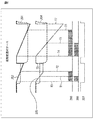
- FIG. 6 is a diagram illustrating an example of A / D conversion of a pixel signal when an output on the low illuminance side is selected.
- a vertical signal line pixel signal 201 that is a waveform of a signal (vertical signal line output) supplied from the pixel 120 to the column ADC via the vertical signal line 108 and a reference signal generation circuit 131 are generated.
- the S / H circuit pixel signal 204 that is the waveform of the output signal of the sample hold unit 170 and the high illuminance signal that is the waveform of the ramp wave generated by the reference signal generation circuit 132.
- An acquisition reference voltage 205 is shown.
- the S / H circuit pixel signal 204 has a waveform substantially similar to that of the vertical signal line pixel signal 201 since the vertical signal line pixel signal 201 is held in the capacitor 172.
- a low illuminance signal acquisition counter 203 indicating the state of counting by the U / D counter 155
- a high illuminance signal acquisition counter 206 indicating the state of counting by the U / D counter 165
- a switch 171 On the lower side of FIG. 6, a low illuminance signal acquisition counter 203 indicating the state of counting by the U / D counter 155, a high illuminance signal acquisition counter 206 indicating the state of counting by the U / D counter 165, and a switch 171.
- a ⁇ S / H207 which is a waveform of a control signal for switching on / off (connection / disconnection), is shown.
- digital CDS is performed to remove fixed pattern noise for each pixel.
- the reset voltage of the FD is read first as the black level of the pixel in the period from time T0 to T3, and the pixel signal (pixel value) of the pixel is read in the period from time T4 to T7. The previously read black level is subtracted from the signal level of the read pixel signal.
- the operation of the digital CDS is arbitrary and may be other than this.
- the frame memory may be placed in the subsequent stage and subtraction processing may be performed, or the obtained black level count value may be inverted (down count) and up-counted as the initial value of the A / D conversion of the pixel signal. .
- ⁇ S / H207 is turned on before T0 when A / D conversion for the reset voltage of the FD is started, and the switch 171 is connected (on). Therefore, the vertical signal line output (FD reset voltage) is held in the capacitor 172.
- ⁇ S / H 207 is turned off, and the switch 171 is turned off (off). In this state, A / D conversion is performed on the reset voltage of the FD from time T0 to T3. Therefore, propagation of signal level fluctuation due to kickback of the comparator 163 is suppressed.
- the high illuminance signal acquisition reference voltage 205 becomes lower than the S / H circuit pixel signal 204, and the output of the comparator 163 is inverted. Therefore, as indicated by the waveform of the high illuminance signal acquisition counter 206, the count by the U / D counter 165 is completed at time T5, and the count value is held.
- the low illuminance signal acquisition reference voltage 202 becomes smaller than the vertical signal line pixel signal 201, and the output of the comparator 153 is inverted. Therefore, as indicated by the waveform of the low illuminance signal acquisition counter 203, the count by the U / D counter 155 ends at time T6, and the count value is held.
- the one with the largest count value and no saturation is selected and output to the subsequent stage. Since the ramp of the high illuminance signal acquisition reference voltage 205 has a steeper slope, the high illuminance signal acquisition counter 206 ends first. Therefore, when the count value of the low illuminance signal acquisition counter 203 is not saturated, the count value of the low illuminance signal acquisition counter 203 is larger.
- the count value of the low-illuminance signal acquisition counter 203 is not saturated, the count value of the U / D counter 155 is selected as an output.
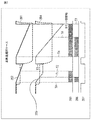
- FIG. 7 is a diagram illustrating an example of A / D conversion of a pixel signal when an output on the high illuminance side is selected.
- the configuration of FIG. 7 is basically the same as that of FIG.
- the high illuminance signal acquisition reference voltage 205 is smaller than the S / H circuit pixel signal 204 at time T8, but the low illuminance signal acquisition reference voltage 202 is the vertical signal by time T7. It is not smaller than the line pixel signal 201. That is, the count value of the low illuminance signal acquisition counter 203 is saturated. In such a case, the count value of the U / D counter 165 is selected as an output.
- the system control unit 106 flags information indicating which signal level is selected and output according to whether the count value of the U / D counter 155 (count value of the low illuminance signal acquisition counter 203) is saturated. And the flag information is output together with the pixel signal.
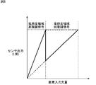
- FIG. 8 shows an example of the relationship between the pixel input light quantity and the sensor output when the illuminance area is divided into two and acquired by two A / D converters.
- the maximum count values are the same, but they are not necessarily the same.
- the light shot noise is random noise having a property of increasing as the illuminance increases, and becomes larger than the kT / C noise at a certain illuminance. It is appropriate to divide the illuminance region so that the kT / C noise increased by the addition of the S / H circuit can be ignored as compared with the light shot noise, and to add the S / H circuit for reading on the high illuminance side. It is also appropriate to determine the gradation of A / D conversion so that quantization noise can be ignored in each illuminance region.
- the CMOS image sensor 100 can acquire a good high-gradation image signal in which the influence of kickback is reduced without sacrificing the frame rate and the number of pixels.
- This technique can reduce power consumption and area as compared with the prior art, and can reduce costs.
- the counter and the comparator are doubled regardless of the number of bits to be increased, and the reference voltage generator is 1 + ⁇ times (1 + ⁇ ⁇ 2 when there are two reference voltage generators).
- the reference voltage generator is 1 + ⁇ times (1 + ⁇ ⁇ 2 when there are two reference voltage generators).
- the circuit block having a current value of 0.25 times increases by one, so the power consumption of the reference voltage generator is 1.25. Is double. Therefore, as compared with the prior art in terms of both power consumption and occupied area, the effect of the present technology increases as the required number of output bits increases.
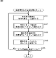
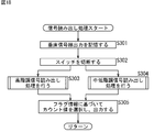
- the image signal output control process is a control process for outputting an image signal as described with reference to FIGS. 6 and 7, for example.
- the system control unit 106 controls the row scanning unit 103, the column scanning unit 105, and the like in step S101, and selects an unprocessed pixel as a processing target (target pixel).
- step S102 the column processing unit 104 performs signal readout processing under the control of the system control unit 106, reads out the reset voltage of the FD of the target pixel as the black level of the pixel, and performs A / D conversion.
- step S103 the column processing unit 104 performs signal readout processing under the control of the system control unit 106, reads out the vertical signal line output as a pixel signal level, and performs A / D conversion.
- step S104 the column processing unit 104 performs digital CDS by subtracting the black level read in step S102 from the pixel signal level read in step S103.
- the system control unit 106 determines whether or not the pixel signals of all the pixels 120 in the pixel array unit 102 have been processed in step S105. If there is an unprocessed pixel, the system control unit 106 returns the process to step S101 and repeats the subsequent processes.
- step S105 If it is determined that all the pixels have been processed in step S105 by repeating the processes in steps S101 to S105 as described above, the system control unit 106 ends the image signal output control process.
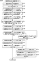
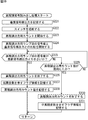
- step S102 and step S103 of FIG. 9 the same signal reading process is executed with only different signals to be processed.
- the signal readout process for the pixel signal performed in step S103 will be described.
- switch 171 is on (connected state) at the start of the signal reading process.
- the capacitor 172 stores the vertical signal line output (pixel signal level of the target pixel) in step S121.
- the switch 171 shifts to a disconnected state (off), and the vertical signal line 108 and the capacitor 161 are electrically connected. Disconnect.
- step S123 the U / D counter 155 and the U / D counter 165 start counting for high gradation output and counting for low gradation output.
- step S124 the comparator 163 starts comparing the signal value of the low gradation output ramp wave with the vertical signal line output (pixel signal level of the target pixel).
- step S125 the comparator 153 starts comparing the signal value of the high gradation output ramp wave with the vertical signal line output (pixel signal level of the target pixel).
- step S126 the comparator 163 determines whether or not the signal value of the low gradation output ramp wave is smaller than the vertical signal line output, and the signal value of the low gradation output ramp wave is smaller than the vertical signal line output. This determination is repeated until it is determined.
- the comparator 163 advances the process to step S127.
- step S127 the U / D counter 165 ends the low gradation output count.
- step S128 the U / D counter 165 stores a count value for low gradation output that is a count value at the time when the count is finished.
- step S129 the comparator 153 determines whether or not the signal value of the high gradation output ramp wave is smaller than the vertical signal line output. In practice, this processing is performed in parallel with the low gradation side processing such as step S126. In this case, since the low gradation side is always inverted first, the low gradation side is inverted. The processing in step S129 will be described. When it is determined that the signal value of the high gradation output ramp wave is smaller than the vertical signal line output, the comparator 153 advances the process to step S130.
- step S130 the U / D counter 155 ends the high gradation output count.
- step S131 the U / D counter 155 outputs flag information indicating the low illuminance side.
- step S132 the U / D counter 155 selects and outputs the high gradation output count value. When the process of step S132 ends, the U / D counter 155 ends the signal reading process and returns the process to FIG.
- step S129 if the comparator 153 determines that the signal value of the high gradation output ramp wave is not smaller than the vertical signal line output, the process proceeds to step S133.
- step S133 the comparator 153 determines whether or not the high gradation output count value is saturated. If it is determined that the count value is not saturated, the process returns to step S129, and the subsequent processing is repeated.
- step S133 If it is determined in step S133 that the A / D conversion for the vertical signal line output has been completed (time T7 has been reached) and the high gradation output count value has been saturated, the comparator 153 performs processing. Proceed to step S134.
- step S134 the U / D counter 155 ends the high gradation output count.
- step S135 the U / D counter 155 outputs flag information indicating the high illuminance side.
- step S136 the U / D counter 165 selects and outputs the low gradation output count value stored in step S128. When the process of step S136 ends, the U / D counter 165 ends the signal reading process and returns the process to FIG.
- the CMOS image sensor 100 can output a higher-quality image with high gradation without sacrificing the frame rate.
- a / D conversion start time control 1 [A / D conversion start time control 1]
- the A / D conversion process of the highest gradation and the A / D conversion process of the other gradations are described to start at the same time.
- the present invention is not limited to this, and starts at different times. You may make it do.
- the effect of kickback reduction can be further enhanced by shifting the start time of a plurality of ramp waves.
- the ramp wave with the slowest slope may be started first, and the comparator 153 for acquiring a high gradation signal may be inverted first.
- the ramp wave with the slowest slope is started first (time T10), and then the voltage value of the ramp wave with the slowest slope and the ramp wave with the steep slope does not intersect.
- a ramp wave with a steep slope may be started at the timing (time T11). Then, the counting by the U / D counter 155 and the U / D counter 165 may be started and ended in accordance with the timing.
- the comparator 153 for acquiring the high gradation signal inverts the output first (time T12). That is, the low illuminance signal acquisition reference voltage 252 is smaller than the vertical signal line (S / H circuit) pixel signal 251 prior to the high illuminance signal acquisition reference voltage 253.
- the kickback generated by the inversion of the comparator 153 may shake the input terminal of the low gradation acquisition comparator 163 via the sample hold unit 170 and may cause a large noise. However, in this case, since the low gradation signal is not selected, no matter how much noise is added to the count value of the U / D counter 165, there is no problem.
- the high gradation signal is saturated (the output of the comparator 153 is not inverted). Does not occur.
- the column ADC 140 can further suppress the propagation of signal level fluctuations due to kickback. That is, the CMOS image sensor 100 can output a higher quality image.
- the count operation for acquiring the low gradation signal by the U / D counter 165 may be stopped when the output of the comparator 155 for acquiring the high gradation signal is inverted. By doing so, the column ADC 140 can reduce execution of unnecessary processing and reduce power consumption.
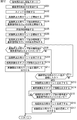
- step S201 and step S202 are performed similarly to each process of step S121 and step S122.
- step S203 the U / D counter 155 starts counting for high gradation output.
- step S204 the comparator 153 starts comparing the signal value of the high gradation output ramp wave with the vertical signal line output (pixel signal level of the target pixel).
- step S205 the U / D counter 165 waits for a predetermined time. Thereafter, the U / D counter 165 starts counting for low gradation output in step S206.
- step S207 the comparator 163 starts comparison between the signal value of the low gradation output ramp wave and the vertical signal line output (pixel signal level of the target pixel).
- or step S214 is performed similarly to each process of step S129 thru
- step S215 as in step S126, the comparator 163 determines whether the signal value of the low gradation output ramp wave is smaller than the vertical signal line output (output of the sample hold unit 170).
- this processing is performed in parallel with the processing on the high gradation side in step S208 and the like. However, in this case, the high gradation side is always inverted first (or saturated), so the high gradation side is saturated. This will be described as the process of later step S215.
- step S215 the comparator 163 repeats this determination until it is determined that the signal value of the low gradation output ramp wave is smaller than the vertical signal line output, and the signal value of the low gradation output ramp wave is the vertical signal line. If it is determined that the output is smaller than the output, the process proceeds to step S216.
- step S216 the U / D counter 165 ends the low gradation output count.
- step S217 the U / D counter 165 selects and outputs a low gradation output count value that is a count value at the time when the count is completed.
- step S217 When the process of step S217 is completed, the U / D counter 165 ends the signal reading process and returns the process to FIG.
- the CMOS image sensor 100 can output a higher quality image.
- a ramp wave with a steep slope may be started first, and a ramp wave with the slowest slope may be started after a predetermined time has elapsed.
- a ramp wave with a steep slope may be started first (time T20), and after a predetermined time has passed (time T21), a ramp wave with the slowest slope may be started. Then, the counting by the U / D counter 155 and the U / D counter 165 may be started and ended in accordance with the timing.
- the voltage values of the respective ramp waves are separated by the amount of waiting for a predetermined time compared to the case described with reference to FIGS. 6 and 7. Therefore, as shown in FIG. 13, even if fluctuation occurs in the signal level of the vertical signal line output due to kickback on the low gradation side (time T22), the fluctuation may induce inversion on the high gradation side. Lower. Thus, if inversion due to kickback does not occur, an accurate count value (time T23) can be obtained even on the high gradation side.
- the column ADC 140 can further suppress the propagation of signal level fluctuations due to kickback. That is, the CMOS image sensor 100 can output a higher quality image.
- step S231 and step S232 are performed similarly to each process of step S121 and step S122.
- step S233 the U / D counter 165 starts counting for low gradation output.
- step S234 the comparator 163 starts comparison between the signal value of the low gradation output ramp wave and the vertical signal line output (pixel signal level of the target pixel).
- step S235 the U / D counter 155 waits for a predetermined time. Thereafter, the U / D counter 155 starts counting for high gradation output in step S236.
- step S237 the comparator 153 starts to compare the signal value of the high gradation output ramp wave with the vertical signal line output (pixel signal level of the target pixel).
- step S238 to step S248 is executed in the same manner as each process from step S129 to step S136.
- the CMOS image sensor 100 can output a higher quality image.
- the processes in steps S201 and S202 may be omitted, and in the case of FIG. 14, the processes in steps S231 and S232 may be omitted. That is, in this case, the signal reading process can be facilitated.
- the range of values that can be taken by the signal level (pixel value) of the vertical signal line output is divided into two areas, a low illuminance area and a high illuminance area. You may divide into.
- signals in a plurality of other illuminance areas may be read during signal reading in the area having the longest readout period.
- FIG. 15 is a diagram showing an example of A / D conversion when the pixel value is located in the medium illuminance region.
- reading of the medium illuminance region (A / D of medium gradation) is performed in parallel with reading of the signal of the low illuminance region having the longest readout time (high gradation A / D conversion). Conversion) and then reading out the high illuminance area (low gradation A / D conversion).
- the reference signal generation circuit 131 starts generating a ramp wave for high gradation with the slowest slope, and at the same time, the reference signal generation circuit 132 has a ramp wave for medium gradation with the second slowest slope. Start generating. Then, while the reference signal generation circuit 131 is generating a ramp wave for high gradation, the reference signal generation circuit 132 sequentially generates a ramp wave for medium gradation and a ramp wave for low gradation with the steepest slope. To do.
- the comparator 163 causes the reference voltage 303 for obtaining the medium illuminance signal to be smaller than the vertical signal line (S / H circuit) pixel signal 301 at time T31. Invert the output. In this case, the value of the low illuminance signal acquisition counter 305 is saturated (the low illuminance signal acquisition reference voltage 302 is not smaller than the vertical signal line (S / H circuit) pixel signal 301).
- the count value of the medium / high illuminance signal acquisition counter 306 is the medium gradation A / D conversion result. Is selected and output.
- FIG. 16 is a diagram showing an example of the state of A / D conversion when the pixel value is located in the high illuminance region.
- the medium illuminance signal acquisition reference voltage 303 is not smaller than the vertical signal line (S / H circuit) pixel signal 301, and at time T41 A / D conversion of gradation is saturated. Thereafter, at time T42, generation of a ramp wave for low gradation with the steepest inclination is started.
- the comparator 163 inverts the output at time T43 when the high illuminance signal acquisition reference voltage 304 becomes smaller than the vertical signal line (S / H circuit) pixel signal 301. Also in this case, the value of the low illuminance signal acquisition counter 305 is saturated (the low illuminance signal acquisition reference voltage 302 is not smaller than the pixel signal 301).
- the count value of the medium / high illuminance signal acquisition counter 306 is low gradation A. Selected as the / D conversion result and output.
- the count value of the low illuminance signal acquisition counter 305 is selected and output as the high gradation A / D conversion result.
- flag information indicating which gradation A / D conversion result is selected and output is also output together with the count value.
- the value of the flag information can be easily set based on whether the A / D conversion of each gradation is saturated, that is, whether the outputs of the comparators 153 and 163 are inverted.
- the flag information when the output of the comparator 153 is inverted, the flag information is set to a value indicating that the selected count value is a high gradation A / D conversion result. Further, for example, when the output of the comparator 153 is not inverted and the output of the comparator 163 is inverted between the time T40 and the time T41, the flag information includes the selected count value of the medium gradation A. Set to a value indicating that this is a / D conversion result.
- the flag information indicates that the selected count value is A Set to a value indicating that this is a / D conversion result.
- the U / D counter 165 may be stopped after time T31. Thus, even if the ramp wave in the subsequent high illuminance region (low gradation signal) is started, the power consumption can be reduced if the counter is not operated.
- FIG. 17 shows an example of the relationship between the pixel input light quantity and the sensor output that can be acquired in this example.
- the maximum count value acquired in the low illuminance area is larger than the sum of the maximum count values in the medium illuminance area and the high illuminance area.
- the column ADC 140 can reduce power consumption and area.
- step S301 and step S302 are performed similarly to each process of step S121 and step S122.
- step S303 the A / D conversion unit on the high gradation side of the column ADC 140 performs high gradation signal read processing and performs high gradation A / D conversion.
- step S304 the A / D conversion unit on the middle / low gradation side (not on the high gradation side) of the column ADC 140 performs medium / low gradation signal readout processing, and performs intermediate gradation and low-order gradation processing. Tone A / D conversion.
- step S303 and step S304 When the processing of step S303 and step S304 ends, the U / D counter 155 and the U / D counter 165 calculate the count value based on the value of the flag information set by the processing of step S303 and step S304 in step S305. Select and output with flag information.
- step S305 When the process of step S305 is completed, the U / D counter 155 and the U / D counter 165 end the signal reading process and return the process to FIG.
- the capacitor 172 stores the vertical signal line output (pixel signal level of the target pixel) in step S321.
- the switch 171 shifts to a disconnected state (off), and the vertical signal line 108 and the capacitor 161 are electrically connected. Disconnect.
- step S323 the U / D counter 155 starts counting for high gradation output.
- step S324 the comparator 153 starts comparing the signal value of the high gradation output ramp wave with the vertical signal line output (pixel signal level of the target pixel).
- step S325 the comparator 153 determines whether or not the signal value of the high gradation output ramp wave is smaller than the vertical signal line output. When it is determined that the signal value of the high gradation output ramp wave is smaller than the vertical signal line output, the comparator 153 advances the process to step S326.
- step S326 the U / D counter 155 ends the high gradation output count.
- step S327 the U / D counter 155 sets and stores flag information indicating the low illuminance side.
- step S328 the U / D counter 155 stores the count value for high gradation output at the time point when the count ends in step S326.
- the U / D counter 155 ends the high gradation signal read process and returns the process to FIG.
- step S325 if the comparator 153 determines that the signal value of the high gradation output ramp wave is not smaller than the vertical signal line output, the process proceeds to step S329.
- step S329 the comparator 153 determines whether or not the high gradation output count value is saturated. If it is determined that the count value is not saturated, the process returns to step S325, and the subsequent processing is repeated.
- step S329 If it is determined in step S329 that the high gradation output count value is saturated, the comparator 153 advances the processing to step S330.
- step S330 the U / D counter 155 ends the high gradation output count.
- step S331 the U / D counter 155 sets and stores flag information indicating the middle / high illuminance side.
- the U / D counter 155 ends the high gradation signal read process and returns the process to FIG.
- the capacitor 172 stores the vertical signal line output (pixel signal level of the target pixel) in step S351.
- the switch 171 shifts to a disconnected state (off), and the vertical signal line 108 and the capacitor 161 are electrically connected. Disconnect.
- step S353 the U / D counter 165 starts counting for medium gradation output.
- step S354 the comparator 163 starts a comparison between the signal value of the ramp wave for middle gradation output and the vertical signal line output (pixel signal level of the target pixel).
- step S355 the comparator 163 determines whether or not the signal value of the ramp wave for medium gradation output is smaller than the vertical signal line output. When it is determined that the signal value of the medium-tone output ramp wave is smaller than the vertical signal line output, the comparator 163 advances the processing to step S356.
- step S356 the U / D counter 165 ends the intermediate gradation output count.
- step S357 the U / D counter 165 sets and stores flag information indicating the middle illuminance side.
- step S358 the U / D counter 165 stores the intermediate gradation output count value at the time point when the count is finished in step S356.
- the U / D counter 165 ends the medium / low gradation signal readout process and returns the process to FIG.
- step S355 if it is determined that the signal value of the ramp wave for medium gradation output is not smaller than the vertical signal line output, the comparator 163 advances the process to step S359.
- step S359 the comparator 163 determines whether or not the medium gradation output count value is saturated. If it is determined that the count value is not saturated, the process returns to step S355, and the subsequent processing is repeated.
- step S359 If it is determined in step S359 that the medium grayscale output count value is saturated, the comparator 163 advances the process to step S360.
- step S360 the U / D counter 165 ends the intermediate gradation output count.
- step S361 the U / D counter 165 sets and stores flag information indicating the high illuminance side.
- step S361 When the process of step S361 ends, the U / D counter 165 starts counting for low gradation output in step S362.
- step S363 the comparator 163 starts a comparison between the signal value of the low gradation output ramp wave and the vertical signal line output (pixel signal level of the target pixel).
- step S364 the comparator 163 determines whether or not the signal value of the low gradation output ramp wave is smaller than the vertical signal line output. When it is determined that the signal value of the low gradation output ramp wave is smaller than the vertical signal line output, the comparator 163 advances the process to step S366.
- step S364 If it is determined in step S364 that the signal value of the low gradation output ramp wave is not smaller than the vertical signal line output, the comparator 163 advances the process to step S365.
- step S365 the comparator 163 determines whether or not the low gradation output count value is saturated. If it is determined that the count value is not saturated, the process returns to step S364, and the subsequent processing is repeated.
- step S365 If it is determined in step S365 that the low gradation output count value is saturated, the comparator 163 advances the process to step S366.
- step S366 the U / D counter 165 ends the low gradation output count.
- step S367 the U / D counter 165 stores the low gradation output count value at the time point when the count is finished in step S366.
- the U / D counter 165 ends the medium / low gradation signal readout process and returns the process to FIG.
- the CMOS image sensor 100 can reduce the power consumption and area of the column ADC 140.
- the column ADC 140 for one vertical signal line has been described as being provided with a plurality of A / D conversion units that perform A / D conversions with different gradations.
- the number of A / D conversion units for each gradation is arbitrary.
- a plurality of A / D conversion units that perform A / D conversion using the same reference signals may be provided.
- FIG. 21 is a block diagram showing a main configuration example of the column ADC in that case.
- the column ADC 440 shown in FIG. 21 is basically the same processing unit as the column ADC 140 described with reference to FIG. However, as shown in FIG. 21, the column ADC 440 has two A / D converters (two columns on the left in the figure) that operate in parallel as A / D converters for high gradation, As the adjustment A / D converter, two A / D converters (two columns on the right in the figure) operating in parallel are provided.
- the A / D converters in the two left columns in the column ADC 440 use the high-gradation A / D conversion reference signal (ramp wave with the slowest slope) generated by the reference signal generation circuit 131. Perform / D conversion. Further, the A / D converters in the two right columns in the column ADC 440 use the low gradation A / D conversion reference signal (ramp wave with a steep slope) generated by the reference signal generation circuit 132 to perform A Perform / D conversion.
- the random noise can be doubled by 1 / ⁇ 2 and the S / N ratio is improved by 3 dB. be able to.
- the number of A / D conversion units to be operated in parallel is arbitrary, and may be three or more. The number is set independently for each gradation. Therefore, the number of A / D conversion units for each gradation may be all the same or may not be the same.
- imaging device imaging device to which the present technology is applied is not limited to the configuration described above, and may have another configuration.
- a plurality of reference signal generation circuits for column ADCs that generate reference signals having ramp waveforms with different inclinations may be provided, and the number may be three or more.
- the column ADC is provided with at least one A / D conversion unit that performs A / D conversion based on each reference signal for one vertical signal line. That is, in the column ADC, A / D conversion of the same number of types of gradations as the number of reference signal generation circuits is performed on one vertical signal line. In this case, A / D conversion of each gradation can be executed in parallel.
- sample hold unit 170 may be provided for each gradation, or, similar to the case of FIG. 5, an A / D conversion unit other than the A / D conversion unit that performs A / D conversion with the highest gradation.
- vertical signal line 108 may be provided only.
- the reference signal generation circuit may be provided outside the column ADC as long as the generated reference signal is supplied to each A / D conversion unit in the column ADC as described above. It may be provided outside the image sensor 100.
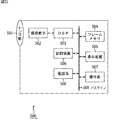
- FIG. 22 is a diagram illustrating a main configuration example of an imaging apparatus to which the present technology is applied.
- An imaging apparatus 500 shown in FIG. 22 is an apparatus that images a subject and outputs an image of the subject as an electrical signal.
- an imaging apparatus 500 includes an optical system including a lens group 501 and the like, an imaging element 502, a DSP (Digital Signal Processor) 503 that is a camera signal processing unit, a frame memory 504, a display apparatus 505, and a recording apparatus. 506, an operation system 507, a power supply system 508, and the like.
- a DSP 503, a frame memory 504, a display device 505, a recording device 506, an operation system 507, and a power supply system 508 are connected to each other via a bus line 509.
- the lens group 501 captures incident light (image light) from a subject and forms an image on the imaging surface of the imaging element 502.
- the imaging element 502 converts the amount of incident light imaged on the imaging surface by the lens group 501 into an electrical signal in units of pixels and outputs it as a pixel signal.
- a solid-state imaging device such as the CMOS image sensor 100 according to the above-described embodiment can be used.
- the DSP 503 performs known camera signal processing.
- the display device 505 includes a liquid crystal display device, an organic EL (electroluminescence) display device, and the like, and displays a moving image or a still image captured by the image sensor 502.
- the recording device 506 records a moving image or a still image captured by the image sensor 502 on a recording medium such as a video tape or a DVD (Digital Versatile Disc).
- the operation system 507 issues operation commands for various functions of the imaging apparatus under operation by the user.
- the power supply system 508 appropriately supplies various power supplies serving as operation power supplies for the DSP 503, the frame memory 504, the display device 505, the recording device 506, and the operation system 507 to these supply targets.
- Such an imaging apparatus 500 is applied to a camera module for a mobile device such as a video camera, a digital still camera, or a mobile phone.
- a camera module for a mobile device such as a video camera, a digital still camera, or a mobile phone.
- the imaging apparatus 500 can reduce the occurrence of noise due to kickback, and can obtain a higher quality captured image.
- the imaging device including the imaging device and the image processing unit to which the present technology is applied is not limited to the configuration described above, and may have another configuration.
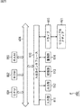
- FIG. 23 is a diagram illustrating a main configuration example of such a general-purpose computer.
- a CPU Central Processing Unit
- a general-purpose computer 600 follows a program stored in a ROM (Read Only Memory) 602 or a program loaded from a storage unit 613 into a RAM (Random Access Memory) 603. Perform various processes.
- the RAM 603 also appropriately stores data necessary for the CPU 601 to execute various processes.
- the CPU 601, ROM 602, and RAM 603 are connected to each other via a bus 604.
- An input / output interface 610 is also connected to the bus 604.
- the input / output interface 610 includes an input unit 611 including a keyboard and a mouse, a display including a CRT (Cathode Ray Tube) and an LCD (Liquid Crystal Display), an output unit 612 including a speaker, a hard disk, and the like.
- a communication unit 614 including a storage unit 613 and a modem is connected. The communication unit 614 performs communication processing via a network including the Internet.
- a drive 615 is connected to the input / output interface 610 as necessary, and a removable medium 621 such as a magnetic disk, an optical disk, a magneto-optical disk, or a semiconductor memory is appropriately mounted, and a computer program read from them is loaded. It is installed in the storage unit 613 as necessary.
- a program constituting the software is installed from a network or a recording medium.
- the recording medium is distributed to distribute a program to a user separately from the apparatus main body, and includes a magnetic disk (including a flexible disk) on which a program is recorded, an optical disk ( It only consists of removable media 621 consisting of CD-ROM (compact disc-read only memory), DVD (including digital versatile disc), magneto-optical disc (including MD (mini disc)), or semiconductor memory. Rather, it is composed of a ROM 602 storing a program and a hard disk included in the storage unit 613, which is distributed to the user in a state of being incorporated in the apparatus main body in advance.
- a magnetic disk including a flexible disk
- an optical disk It only consists of removable media 621 consisting of CD-ROM (compact disc-read only memory), DVD (including digital versatile disc), magneto-optical disc (including MD (mini disc)), or semiconductor memory. Rather, it is composed of a ROM 602 storing a program and a hard disk included in the storage unit 613, which is distributed to the user in a state
- the program executed by the computer may be a program that is processed in time series in the order described in this specification, or in parallel or at a necessary timing such as when a call is made. It may be a program for processing.
- the step of describing the program recorded on the recording medium is not limited to the processing performed in chronological order according to the described order, but may be performed in parallel or It also includes processes that are executed individually.
- system represents the entire apparatus composed of a plurality of devices (apparatuses).
- the configuration described as one device (or processing unit) may be divided and configured as a plurality of devices (or processing units).
- the configurations described above as a plurality of devices (or processing units) may be combined into a single device (or processing unit).
- a configuration other than that described above may be added to the configuration of each device (or each processing unit).
- a part of the configuration of a certain device (or processing unit) may be included in the configuration of another device (or other processing unit). . That is, the present technology is not limited to the above-described embodiment, and various modifications can be made without departing from the gist of the present technology.
- this technique can also take the following structures.
- a plurality of comparison units that compare an analog signal supplied from a pixel including a photoelectric conversion element via a vertical signal line with reference signals of ramp waves having different inclinations and output a comparison result;
- a plurality of counters that count until the comparison result is inverted for the different comparison units, and output the count value as digital data;
- the comparison unit that compares the analog signal with a reference signal of a ramp wave other than the ramp wave having the slowest slope holds the analog signal supplied through the vertical signal line before starting the comparison.
- a sample hold unit for electrically disconnecting the vertical signal line and the comparison unit and supplying the held analog signal to the comparison unit while the comparison unit performs the comparison;
- An image sensor provided.
- the sample hold unit includes: A switch for electrically connecting or disconnecting between the vertical signal line and the comparison unit; The analog signal supplied via the vertical signal line is held while the vertical signal line and the comparison unit are electrically connected by the switch, and the vertical signal line and the comparison unit are retained. And the capacitor that supplies the analog signal held by itself to the comparison unit while being electrically disconnected from the image pickup device. .
- the reference signal generation unit that generates the reference signal of the ramp wave having the other slope at the timing before the reference signal generation unit that generates the reference signal of the ramp wave having the gentlest inclination generates the reference signal. Starts generating the reference signal.
- the imaging device according to (7) (11) While the reference signal generation unit that generates the reference signal of the ramp wave with the gentlest inclination generates the reference signal, the reference signal generation unit that generates the reference signal of the ramp wave of the other inclination, The imaging device according to (7), wherein ramp wave reference signals having different inclinations are sequentially generated.
- a part or all of the plurality of comparison units compares the analog signal with a reference signal of a ramp wave having the same slope, (1) to (11) further including an addition averaging unit that adds and averages the count values output from counters corresponding to each of a plurality of comparison units that compare the analog signal with reference signals of ramp waves having the same slope. ).
- a method for controlling an image sensor A plurality of comparison units compare an analog signal supplied from a pixel including a photoelectric conversion element via a vertical signal line with a reference signal of a ramp wave having a different slope, and outputs a comparison result, A plurality of counters counts the comparison units different from each other until the comparison result is inverted, and outputs the count value as digital data.
- the sample-and-hold unit compares the analog signal with a reference signal of a ramp wave other than the ramp wave having the slowest slope, and is supplied via the vertical signal line before the comparison unit starts the comparison. While the analog signal is held and the comparison unit performs the comparison, the vertical signal line and the comparison unit are electrically disconnected and the held analog signal is supplied to the comparison unit. Control method.
- (14) a plurality of comparison units that compare an analog signal supplied from a pixel including a photoelectric conversion element via a vertical signal line with reference signals of ramp waves having different inclinations and output a comparison result; A plurality of counters that count until the comparison result is inverted for the different comparison units, and output the count value as digital data;
- the comparison unit that compares the analog signal with a reference signal of a ramp wave other than the ramp wave having the slowest slope holds the analog signal supplied through the vertical signal line before starting the comparison.
- a sample hold unit for electrically disconnecting the vertical signal line and the comparison unit and supplying the held analog signal to the comparison unit while the comparison unit performs the comparison;
- An image sensor having An image processing unit that performs image processing on digital data of a captured image output from the imaging element;
- a storage unit that stores digital data of the captured image that has been subjected to image processing by the image processing unit.
- a plurality of reference signal generation units that generate ramp wave reference signals having different inclinations at different timings;
- a plurality of comparison units that compare an analog signal supplied from a pixel including a photoelectric conversion element via a vertical signal line with the reference signal generated by the different reference signal generation units, and output a comparison result;
- An imaging device comprising: a plurality of counters that count until the comparison result is inverted and output the count value as digital data for the different comparison units.
- the imaging device wherein the reference signal generation unit that generates a reference signal of a ramp wave having another slope starts generating the reference signal.
- the reference signal generation unit that generates the reference signal of the ramp wave having the other slope at the timing before the reference signal generation unit that generates the reference signal of the ramp wave having the gentlest inclination generates the reference signal. Starts generating the reference signal.
- the imaging device (18) The image sensor according to (15), wherein flag information indicating a voltage range of a reference signal used by a comparator corresponding to the selected counter is output together with the count value.
- a method of controlling an image sensor A plurality of reference signal generation units generate ramp wave reference signals having different slopes at different timings, A plurality of comparison units compare an analog signal supplied from a pixel including a photoelectric conversion element via a vertical signal line with the reference signal generated by the different reference signal generation unit, and outputs a comparison result, A control method in which a plurality of counters count until the comparison result is inverted for the different comparison units, and output the count value as digital data.
- a plurality of reference signal generation units that generate ramp wave reference signals having different inclinations at different timings
- a plurality of comparison units that compare an analog signal supplied from a pixel including a photoelectric conversion element via a vertical signal line with the reference signal generated by the different reference signal generation units, and output a comparison result
- An imaging device having a plurality of counters that count until the comparison result is inverted and output the count value as digital data for the different comparison units
- An image processing unit that performs image processing on digital data of a captured image output from the imaging element
- a storage unit that stores digital data of the captured image that has been subjected to image processing by the image processing unit.
- CMOS image sensor 101 semiconductor substrate, 102 pixel array unit, 103 row scanning unit, 104 column processing unit, 105 column scanning unit, 106 system control unit, 107 pixel drive line, 108 vertical signal line, 109 horizontal bus, 110 output Terminal, 120 pixels, 131 and 132 reference signal generation circuit, 140 column ADC, 153 comparator, 155 U / D counter, 163 comparator, 165 U / D counter, 170 sample hold unit, 171 switch, 172 capacitor, 440 column ADC, 470 sample hold unit, 491 addition average calculation unit, 500 imaging device, 600 computer
Landscapes
- Engineering & Computer Science (AREA)
- Multimedia (AREA)
- Signal Processing (AREA)
- Theoretical Computer Science (AREA)
- Transforming Light Signals Into Electric Signals (AREA)
- Analogue/Digital Conversion (AREA)
Abstract
Description
1.第1の実施の形態(イメージセンサ)
2.第2の実施の形態(撮像装置)
3.第3の実施の形態(コンピュータ)
[積分型A/D変換]
最初に、ランプ波形を参照電圧として利用する積分型A/D(Analog / Digital)変換について説明する。ランプ波形を参照電圧とした時間積分型のA/D変換器は、線形性やノイズ特性が良く、他のA/D変換方式と比較してCMOS(Complementary Metal Oxide Semiconductor)イメージセンサとの相性が良いので、CMOSイメージセンサにおいて広く利用されている。
そこで、本開示では、このようなキックバックによるノイズの発生を抑制する技術について説明する。
図4は、画素120の回路構成の一例を示す回路図である。図4に示されるように、画素120は、光電変換部である例えばフォトダイオード121に加えて、例えば転送トランジスタ122、リセットトランジスタ123、増幅トランジスタ124、および選択トランジスタ125の4つのトランジスタを有する。
図5は、カラム処理部104のカラムADCの主な構成例を示すブロック図である。図5に示されるカラムADC140は、1垂直信号線分の構成例である。図5に示される構成のカラムADC140は、各垂直信号線に対して設けられる。
以下に具体的な動作例について説明する。最初に低照度側の出力が選択されるケース(画素値が小さい場合)について説明する。図6は、低照度側の出力が選択される場合の、画素信号のA/D変換の様子の例を示す図である。
次に、以上のようなCMOSイメージセンサ100により実行される処理について説明する。最初に、図9のフローチャートを参照して、画像信号出力制御処理の流れの例を説明する。画像信号出力制御処理は、例えば図6や図7を参照して説明したように画像信号を出力させるための制御処理である。
次に、図10のフローチャートを参照して、図9のステップS102またはステップS103において実行される信号読み出し処理の流れの例を説明する。
以上においては、最も高階調のA/D変換処理と、それ以外の階調のA/D変換処理とを互いに同時刻に開始するように説明したが、これに限らず、互いに異なる時刻に開始するようにしてもよい。
この場合も、画像信号出力制御処理は、図9のフローチャートを参照して説明した場合と同様に実行される。ただし、信号読み出し処理は、図12のフローチャートのように実行される。図12のフローチャートを参照して、その信号読み出し処理の流れの例を説明する。なお、ステップS102の処理とステップS103の処理は互いに同様に実行されるので、以下においては、図10の場合と同様に、ステップS103の画素信号レベルのA/D変換についてのみ説明する。
また、逆に、例えば、図13に示されるように、傾斜の急なランプ波を先に開始させ、所定時間経過後に、最も傾斜の緩やかなランプ波を開始させるようにしてもよい。
この場合も、画像信号出力制御処理は、図9のフローチャートを参照して説明した場合と同様に実行される。ただし、信号読み出し処理は、図14のフローチャートのように実行される。図14のフローチャートを参照して、その信号読み出し処理の流れの例を説明する。なお、ステップS102の処理とステップS103の処理は互いに同様に実行されるので、以下においては、図10の場合と同様に、ステップS103の画素信号レベルのA/D変換についてのみ説明する。
なお、上述したように、最も高階調のA/D変換処理、および、それ以外の階調のA/D変換処理を、互いに異なる時刻に開始するようにするだけでも、キックバックの影響の伝搬を抑制することができる。したがって、この場合、サンプルホールド部170を省略し、その入出力を常時短絡させる(低階調側のA/D変換部の構成であるコンデンサ161を常時垂直信号線108に接続する)ようにしてもよい。このようにすることにより、カラムADC140の構成をより簡易化することができる。
以上においては、垂直信号線出力の信号レベル(画素値)が取り得る値の範囲を低照度領域と高照度領域の2つに分割したが、分割後の領域数は任意であり、3領域以上に分割してもよい。
この場合も、画像信号出力制御処理は、図9のフローチャートを参照して説明した場合と同様に実行される。ただし、信号読み出し処理は、図18のフローチャートのように実行される。図18のフローチャートを参照して、その信号読み出し処理の流れの例を説明する。なお、ステップS102の処理とステップS103の処理は互いに同様に実行されるので、以下においては、図10の場合と同様に、ステップS103の画素信号レベルのA/D変換についてのみ説明する。
次に、図19のフローチャートを参照して、図18のステップS303において実行される高階調信号読み出し処理の流れの例を説明する。
次に、図20のフローチャートを参照して、図18のステップS304において実行される中低階調信号読み出し処理の流れの例を説明する。
以上においては、1垂直信号線に対するカラムADC140として、互いに異なる階調のA/D変換を行う複数のA/D変換部を設けるように説明したが、各階調のA/D変換部は、1つずつであるように説明した。しかしながら、各階調のA/D変換部の数は任意である。例えば、互いに同一の参照信号(同じ傾きのランプ波)を用いてA/D変換を行う複数のA/D変換部を設けるようにしてもよい。
[撮像装置]
図22は、本技術を適用した撮像装置の主な構成例を示す図である。図22に示される撮像装置500は、被写体を撮像し、その被写体の画像を電気信号として出力する装置である。図22に示されるように、撮像装置500は、レンズ群501等を含む光学系、撮像素子502、カメラ信号処理部であるDSP(Digital Signal Processor)503、フレームメモリ504、表示装置505、記録装置506、操作系507、および電源系508等を有する。そして、DSP503、フレームメモリ504、表示装置505、記録装置506、操作系507、および電源系508がバスライン509を介して相互に接続されている。
[コンピュータ]
上述した一連の処理は、ハードウエアにより実行することもできるし、ソフトウエアにより実行することもできる。一連の処理をソフトウエアにより実行する場合には、そのソフトウエアを構成するプログラムが、コンピュータにインストールされる。ここで、コンピュータには、例えば、図3のシステム制御部106のような、専用のハードウエアに組み込まれているコンピュータや、各種のプログラムをインストールすることで各種の機能を実行することが可能な汎用のコンピュータなどが含まれる。
(1) 光電変換素子を含む画素から垂直信号線を介して供給されるアナログ信号を、傾きが互いに異なるランプ波の参照信号と比較し、比較結果を出力する複数の比較部と、
互いに異なる前記比較部について、前記比較結果が反転するまでをカウントし、カウント値をデジタルデータとして出力する複数のカウンタと、
前記アナログ信号と傾きが最も緩やかなランプ波以外のランプ波の参照信号との比較を行う前記比較部が前記比較を開始する前に、前記垂直信号線を介して供給される前記アナログ信号を保持し、前記比較部が前記比較を行う間、前記垂直信号線と前記比較部との間を電気的に切断するとともに、保持している前記アナログ信号を前記比較部に供給するサンプルホールド部と
を備える撮像素子。
(2) 傾きが最も緩やかなランプ波の電圧範囲は、kT/Cノイズが全てのノイズで最も支配的である範囲で動作する
前記(1)に記載の撮像素子。
(3) 複数の前記カウンタの中から各比較部の比較結果に基づいて選択された、前記アナログ信号を前記アナログ信号の信号レベルに応じた照度領域に対応する参照信号と比較する比較部についてのカウントを行うカウンタが、前記カウント値を出力する
前記(2)に記載の撮像素子。
(4) 複数の前記カウンタの内、カウント値が最も大きく、かつ、自身が対応する前記比較部の前記比較結果が反転しているカウンタが選択される
前記(3)に記載の撮像素子。
(5) 選択されたカウンタが対応する比較器が利用する参照信号の電圧範囲を示すフラグ情報が、前記カウント値とともに出力される
前記(4)に記載の撮像素子。
(6) 前記サンプルホールド部は、
前記垂直信号線と前記比較部との間を電気的に接続したり切断したりするスイッチと、
前記スイッチにより前記垂直信号線と前記比較部との間を電気的に接続されている間に、前記垂直信号線を介して供給される前記アナログ信号を保持し、前記垂直信号線と前記比較部との間を電気的に切断されている間に、自身が保持している前記アナログ信号を前記比較部に供給するコンデンサと
を備える前記(1)乃至(5)のいずれかに記載の撮像素子。
(7) 傾きが互いに異なるランプ波の参照信号を生成する複数の参照信号生成部をさらに備え、
複数の前記比較部は、前記アナログ信号を、互いに異なる前記参照信号生成部により生成された参照信号と比較する
前記(1)乃至(6)のいずれかに記載の撮像素子。
(8) 複数の前記参照信号生成部は、互いに同一のタイミングで前記参照信号の生成を開始する
前記(7)に記載の撮像素子。
(9)
傾きが最も緩やかなランプ波の参照信号を生成する前記参照信号生成部が前記参照信号を生成した後、前記ランプ波とその他の傾きのランプ波とが電圧的に交差しないタイミングにおいて、その他の傾きのランプ波の参照信号を生成する前記参照信号生成部が、前記参照信号の生成を開始する
前記(7)に記載の撮像素子。
(10) 傾きが最も緩やかなランプ波の参照信号を生成する前記参照信号生成部が前記参照信号を生成する前のタイミングにおいて、その他の傾きのランプ波の参照信号を生成する前記参照信号生成部が、前記参照信号の生成を開始する
前記(7)に記載の撮像素子。
(11) 傾きが最も緩やかなランプ波の参照信号を生成する前記参照信号生成部が前記参照信号を生成する間に、その他の傾きのランプ波の参照信号を生成する前記参照信号生成部が、互いに傾きが異なるランプ波の参照信号を順次生成する
前記(7)に記載の撮像素子。
(12) 複数の前記比較部の一部または全部が、前記アナログ信号を、傾きが互いに同一のランプ波の参照信号と比較し、
前記アナログ信号を、傾きが互いに同一のランプ波の参照信号と比較する複数の比較部のそれぞれに対応するカウンタが出力するカウント値を加算平均する加算平均部をさらに備える
前記(1)乃至(11)のいずれかに記載の撮像素子。
(13) 撮像素子の制御方法であって、
複数の比較部が、光電変換素子を含む画素から垂直信号線を介して供給されるアナログ信号を、傾きが互いに異なるランプ波の参照信号と比較し、比較結果を出力し、
複数のカウンタが、互いに異なる前記比較部について、前記比較結果が反転するまでをカウントし、カウント値をデジタルデータとして出力し、
サンプルホールド部が、前記アナログ信号と傾きが最も緩やかなランプ波以外のランプ波の参照信号との比較を行う前記比較部が前記比較を開始する前に、前記垂直信号線を介して供給される前記アナログ信号を保持し、前記比較部が前記比較を行う間、前記垂直信号線と前記比較部との間を電気的に切断するとともに、保持している前記アナログ信号を前記比較部に供給する
制御方法。
(14) 光電変換素子を含む画素から垂直信号線を介して供給されるアナログ信号を、傾きが互いに異なるランプ波の参照信号と比較し、比較結果を出力する複数の比較部と、
互いに異なる前記比較部について、前記比較結果が反転するまでをカウントし、カウント値をデジタルデータとして出力する複数のカウンタと、
前記アナログ信号と傾きが最も緩やかなランプ波以外のランプ波の参照信号との比較を行う前記比較部が前記比較を開始する前に、前記垂直信号線を介して供給される前記アナログ信号を保持し、前記比較部が前記比較を行う間、前記垂直信号線と前記比較部との間を電気的に切断するとともに、保持している前記アナログ信号を前記比較部に供給するサンプルホールド部と
を有する撮像素子と、
前記撮像素子より出力される撮像画像のデジタルデータを画像処理する画像処理部と、
前記画像処理部により画像処理された前記撮像画像のデジタルデータを記憶する記憶部と
を備える撮像装置。
(15) 傾きが互いに異なるランプ波の参照信号を、互いに異なるタイミングで生成する複数の参照信号生成部と、
光電変換素子を含む画素から垂直信号線を介して供給されるアナログ信号を、互いに異なる前記参照信号生成部が生成した前記参照信号と比較し、比較結果を出力する複数の比較部と、
互いに異なる前記比較部について、前記比較結果が反転するまでをカウントし、カウント値をデジタルデータとして出力する複数のカウンタと
を備える撮像素子。
(16) 傾きが最も緩やかなランプ波の参照信号を生成する前記参照信号生成部が前記参照信号を生成した後、前記ランプ波とその他の傾きのランプ波とが電圧的に交差しないタイミングにおいて、その他の傾きのランプ波の参照信号を生成する前記参照信号生成部が、前記参照信号の生成を開始する
前記(15)に記載の撮像素子。
(17) 傾きが最も緩やかなランプ波の参照信号を生成する前記参照信号生成部が前記参照信号を生成する前のタイミングにおいて、その他の傾きのランプ波の参照信号を生成する前記参照信号生成部が、前記参照信号の生成を開始する
前記(15)に記載の撮像素子。
(18)
選択されたカウンタが対応する比較器が利用する参照信号の電圧範囲を示すフラグ情報が、前記カウント値とともに出力される
前記(15)に記載の撮像素子。
(19) 撮像素子の制御方法であって、
複数の参照信号生成部が、傾きが互いに異なるランプ波の参照信号を、互いに異なるタイミングで生成し、
複数の比較部が、光電変換素子を含む画素から垂直信号線を介して供給されるアナログ信号を、互いに異なる前記参照信号生成部が生成した前記参照信号と比較し、比較結果を出力し、
複数のカウンタが、互いに異なる前記比較部について、前記比較結果が反転するまでをカウントし、カウント値をデジタルデータとして出力する
制御方法。
(20) 傾きが互いに異なるランプ波の参照信号を、互いに異なるタイミングで生成する複数の参照信号生成部と、
光電変換素子を含む画素から垂直信号線を介して供給されるアナログ信号を、互いに異なる前記参照信号生成部が生成した前記参照信号と比較し、比較結果を出力する複数の比較部と、
互いに異なる前記比較部について、前記比較結果が反転するまでをカウントし、カウント値をデジタルデータとして出力する複数のカウンタと
を有する撮像素子と、
前記撮像素子より出力される撮像画像のデジタルデータを画像処理する画像処理部と、
前記画像処理部により画像処理された前記撮像画像のデジタルデータを記憶する記憶部と
を備える撮像装置。
Claims (20)
- 光電変換素子を含む画素から垂直信号線を介して供給されるアナログ信号を、傾きが互いに異なるランプ波の参照信号と比較し、比較結果を出力する複数の比較部と、
互いに異なる前記比較部について、前記比較結果が反転するまでをカウントし、カウント値をデジタルデータとして出力する複数のカウンタと、
前記アナログ信号と傾きが最も緩やかなランプ波以外のランプ波の参照信号との比較を行う前記比較部が前記比較を開始する前に、前記垂直信号線を介して供給される前記アナログ信号を保持し、前記比較部が前記比較を行う間、前記垂直信号線と前記比較部との間を電気的に切断するとともに、保持している前記アナログ信号を前記比較部に供給するサンプルホールド部と
を備える撮像素子。 - 傾きが最も緩やかなランプ波の電圧範囲は、kT/Cノイズが全てのノイズで最も支配的である範囲で動作する
請求項1に記載の撮像素子。 - 複数の前記カウンタの中から各比較部の比較結果に基づいて選択された、前記アナログ信号を前記アナログ信号の信号レベルに応じた照度領域に対応する参照信号と比較する比較部についてのカウントを行うカウンタが、前記カウント値を出力する
請求項2に記載の撮像素子。 - 複数の前記カウンタの内、カウント値が最も大きく、かつ、自身が対応する前記比較部の前記比較結果が反転しているカウンタが選択される
請求項3に記載の撮像素子。 - 選択されたカウンタが対応する比較器が利用する参照信号の電圧範囲を示すフラグ情報が、前記カウント値とともに出力される
請求項4に記載の撮像素子。 - 前記サンプルホールド部は、
前記垂直信号線と前記比較部との間を電気的に接続したり切断したりするスイッチと、
前記スイッチにより前記垂直信号線と前記比較部との間を電気的に接続されている間に、前記垂直信号線を介して供給される前記アナログ信号を保持し、前記垂直信号線と前記比較部との間を電気的に切断されている間に、自身が保持している前記アナログ信号を前記比較部に供給するコンデンサと
を備える請求項1に記載の撮像素子。 - 傾きが互いに異なるランプ波の参照信号を生成する複数の参照信号生成部をさらに備え、
複数の前記比較部は、前記アナログ信号を、互いに異なる前記参照信号生成部により生成された参照信号と比較する
請求項1に記載の撮像素子。 - 複数の前記参照信号生成部は、互いに同一のタイミングで前記参照信号の生成を開始する
請求項7に記載の撮像素子。 - 傾きが最も緩やかなランプ波の参照信号を生成する前記参照信号生成部が前記参照信号を生成した後、前記ランプ波とその他の傾きのランプ波とが電圧的に交差しないタイミングにおいて、その他の傾きのランプ波の参照信号を生成する前記参照信号生成部が、前記参照信号の生成を開始する
請求項7に記載の撮像素子。 - 傾きが最も緩やかなランプ波の参照信号を生成する前記参照信号生成部が前記参照信号を生成する前のタイミングにおいて、その他の傾きのランプ波の参照信号を生成する前記参照信号生成部が、前記参照信号の生成を開始する
請求項7に記載の撮像素子。 - 傾きが最も緩やかなランプ波の参照信号を生成する前記参照信号生成部が前記参照信号を生成する間に、その他の傾きのランプ波の参照信号を生成する前記参照信号生成部が、互いに傾きが異なるランプ波の参照信号を順次生成する
請求項7に記載の撮像素子。 - 複数の前記比較部の一部または全部が、前記アナログ信号を、傾きが互いに同一のランプ波の参照信号と比較し、
前記アナログ信号を、傾きが互いに同一のランプ波の参照信号と比較する複数の比較部のそれぞれに対応するカウンタが出力するカウント値を加算平均する加算平均部をさらに備える
請求項1に記載の撮像素子。 - 撮像素子の制御方法であって、
複数の比較部が、光電変換素子を含む画素から垂直信号線を介して供給されるアナログ信号を、傾きが互いに異なるランプ波の参照信号と比較し、比較結果を出力し、
複数のカウンタが、互いに異なる前記比較部について、前記比較結果が反転するまでをカウントし、カウント値をデジタルデータとして出力し、
サンプルホールド部が、前記アナログ信号と傾きが最も緩やかなランプ波以外のランプ波の参照信号との比較を行う前記比較部が前記比較を開始する前に、前記垂直信号線を介して供給される前記アナログ信号を保持し、前記比較部が前記比較を行う間、前記垂直信号線と前記比較部との間を電気的に切断するとともに、保持している前記アナログ信号を前記比較部に供給する
制御方法。 - 光電変換素子を含む画素から垂直信号線を介して供給されるアナログ信号を、傾きが互いに異なるランプ波の参照信号と比較し、比較結果を出力する複数の比較部と、
互いに異なる前記比較部について、前記比較結果が反転するまでをカウントし、カウント値をデジタルデータとして出力する複数のカウンタと、
前記アナログ信号と傾きが最も緩やかなランプ波以外のランプ波の参照信号との比較を行う前記比較部が前記比較を開始する前に、前記垂直信号線を介して供給される前記アナログ信号を保持し、前記比較部が前記比較を行う間、前記垂直信号線と前記比較部との間を電気的に切断するとともに、保持している前記アナログ信号を前記比較部に供給するサンプルホールド部と
を有する撮像素子と、
前記撮像素子より出力される撮像画像のデジタルデータを画像処理する画像処理部と、
前記画像処理部により画像処理された前記撮像画像のデジタルデータを記憶する記憶部と
を備える撮像装置。 - 傾きが互いに異なるランプ波の参照信号を、互いに異なるタイミングで生成する複数の参照信号生成部と、
光電変換素子を含む画素から垂直信号線を介して供給されるアナログ信号を、互いに異なる前記参照信号生成部が生成した前記参照信号と比較し、比較結果を出力する複数の比較部と、
互いに異なる前記比較部について、前記比較結果が反転するまでをカウントし、カウント値をデジタルデータとして出力する複数のカウンタと
を備える撮像素子。 - 傾きが最も緩やかなランプ波の参照信号を生成する前記参照信号生成部が前記参照信号を生成した後、前記ランプ波とその他の傾きのランプ波とが電圧的に交差しないタイミングにおいて、その他の傾きのランプ波の参照信号を生成する前記参照信号生成部が、前記参照信号の生成を開始する
請求項15に記載の撮像素子。 - 傾きが最も緩やかなランプ波の参照信号を生成する前記参照信号生成部が前記参照信号を生成する前のタイミングにおいて、その他の傾きのランプ波の参照信号を生成する前記参照信号生成部が、前記参照信号の生成を開始する
請求項15に記載の撮像素子。 - 選択されたカウンタが対応する比較器が利用する参照信号の電圧範囲を示すフラグ情報が、前記カウント値とともに出力される
請求項15に記載の撮像素子。 - 撮像素子の制御方法であって、
複数の参照信号生成部が、傾きが互いに異なるランプ波の参照信号を、互いに異なるタイミングで生成し、
複数の比較部が、光電変換素子を含む画素から垂直信号線を介して供給されるアナログ信号を、互いに異なる前記参照信号生成部が生成した前記参照信号と比較し、比較結果を出力し、
複数のカウンタが、互いに異なる前記比較部について、前記比較結果が反転するまでをカウントし、カウント値をデジタルデータとして出力する
制御方法。 - 傾きが互いに異なるランプ波の参照信号を、互いに異なるタイミングで生成する複数の参照信号生成部と、
光電変換素子を含む画素から垂直信号線を介して供給されるアナログ信号を、互いに異なる前記参照信号生成部が生成した前記参照信号と比較し、比較結果を出力する複数の比較部と、
互いに異なる前記比較部について、前記比較結果が反転するまでをカウントし、カウント値をデジタルデータとして出力する複数のカウンタと
を有する撮像素子と、
前記撮像素子より出力される撮像画像のデジタルデータを画像処理する画像処理部と、
前記画像処理部により画像処理された前記撮像画像のデジタルデータを記憶する記憶部と
を備える撮像装置。
Priority Applications (5)
| Application Number | Priority Date | Filing Date | Title |
|---|---|---|---|
| KR1020147009969A KR101979473B1 (ko) | 2011-12-08 | 2012-11-30 | 촬상 소자, 제어 방법, 및, 촬상 장치 |
| JP2013548207A JP6040942B2 (ja) | 2011-12-08 | 2012-11-30 | 撮像素子、制御方法、並びに、撮像装置 |
| CN201280069321.6A CN104115488B (zh) | 2011-12-08 | 2012-11-30 | 成像元件、控制方法和成像设备 |
| US14/356,011 US9100606B2 (en) | 2011-12-08 | 2012-11-30 | Imaging element, control method, and imaging apparatus |
| US14/796,657 US9584749B2 (en) | 2011-12-08 | 2015-07-10 | Imaging element, control method, and imaging apparatus |
Applications Claiming Priority (2)
| Application Number | Priority Date | Filing Date | Title |
|---|---|---|---|
| JP2011-268896 | 2011-12-08 | ||
| JP2011268896 | 2011-12-08 |
Related Child Applications (2)
| Application Number | Title | Priority Date | Filing Date |
|---|---|---|---|
| US14/356,011 A-371-Of-International US9100606B2 (en) | 2011-12-08 | 2012-11-30 | Imaging element, control method, and imaging apparatus |
| US14/796,657 Continuation US9584749B2 (en) | 2011-12-08 | 2015-07-10 | Imaging element, control method, and imaging apparatus |
Publications (1)
| Publication Number | Publication Date |
|---|---|
| WO2013084809A1 true WO2013084809A1 (ja) | 2013-06-13 |
Family
ID=48574177
Family Applications (1)
| Application Number | Title | Priority Date | Filing Date |
|---|---|---|---|
| PCT/JP2012/081053 Ceased WO2013084809A1 (ja) | 2011-12-08 | 2012-11-30 | 撮像素子、制御方法、並びに、撮像装置 |
Country Status (6)
| Country | Link |
|---|---|
| US (2) | US9100606B2 (ja) |
| JP (1) | JP6040942B2 (ja) |
| KR (1) | KR101979473B1 (ja) |
| CN (1) | CN104115488B (ja) |
| TW (1) | TWI530183B (ja) |
| WO (1) | WO2013084809A1 (ja) |
Cited By (25)
| Publication number | Priority date | Publication date | Assignee | Title |
|---|---|---|---|---|
| JP2014146849A (ja) * | 2013-01-25 | 2014-08-14 | Canon Inc | 撮像装置、その駆動方法、及び撮像システム |
| JP2015104021A (ja) * | 2013-11-26 | 2015-06-04 | キヤノン株式会社 | 撮像素子、撮像装置及び携帯電話機 |
| JP2015106816A (ja) * | 2013-11-29 | 2015-06-08 | キヤノン株式会社 | 撮像装置、撮像システム、撮像装置の駆動方法、撮像システムの駆動方法 |
| JP2015162751A (ja) * | 2014-02-26 | 2015-09-07 | キヤノン株式会社 | 光電変換装置および撮像システム |
| WO2015159729A1 (ja) * | 2014-04-16 | 2015-10-22 | ソニー株式会社 | 撮像素子、制御方法、プログラム、および電子機器 |
| WO2015183953A1 (en) * | 2014-05-30 | 2015-12-03 | Seek Thermal, Inc. | Data digitization and display for an imaging system |
| WO2016072280A1 (ja) * | 2014-11-05 | 2016-05-12 | ソニー株式会社 | 信号処理装置、撮像素子、並びに電子機器 |
| JP2017005392A (ja) * | 2015-06-05 | 2017-01-05 | キヤノン株式会社 | 撮像装置、撮像システム |
| US9549130B2 (en) | 2015-05-01 | 2017-01-17 | Seek Thermal, Inc. | Compact row column noise filter for an imaging system |
| CN106416229A (zh) * | 2013-12-06 | 2017-02-15 | 株式会社尼康 | 拍摄元件以及拍摄装置 |
| US9584750B2 (en) | 2014-08-20 | 2017-02-28 | Seek Thermal, Inc. | Adaptive adjustment of the operating bias of an imaging system |
| US9595934B2 (en) | 2014-08-20 | 2017-03-14 | Seek Thermal, Inc. | Gain calibration for an imaging system |
| CN106576149A (zh) * | 2014-08-19 | 2017-04-19 | 索尼公司 | 固态摄像元件和电子装置 |
| US9727954B2 (en) | 2014-08-05 | 2017-08-08 | Seek Thermal, Inc. | Local contrast adjustment for digital images |
| US9924116B2 (en) | 2014-08-05 | 2018-03-20 | Seek Thermal, Inc. | Time based offset correction for imaging systems and adaptive calibration control |
| US9930324B2 (en) | 2014-08-05 | 2018-03-27 | Seek Thermal, Inc. | Time based offset correction for imaging systems |
| US9947086B2 (en) | 2014-12-02 | 2018-04-17 | Seek Thermal, Inc. | Image adjustment based on locally flat scenes |
| US10467736B2 (en) | 2014-12-02 | 2019-11-05 | Seek Thermal, Inc. | Image adjustment based on locally flat scenes |
| US10600164B2 (en) | 2014-12-02 | 2020-03-24 | Seek Thermal, Inc. | Image adjustment based on locally flat scenes |
| US10867371B2 (en) | 2016-06-28 | 2020-12-15 | Seek Thermal, Inc. | Fixed pattern noise mitigation for a thermal imaging system |
| US11276152B2 (en) | 2019-05-28 | 2022-03-15 | Seek Thermal, Inc. | Adaptive gain adjustment for histogram equalization in an imaging system |
| JP7094852B2 (ja) | 2018-10-04 | 2022-07-04 | 株式会社ニコン | 撮像素子および撮像装置 |
| JP2022158017A (ja) * | 2021-04-01 | 2022-10-14 | キヤノン株式会社 | 信号処理装置 |
| JP2022162974A (ja) * | 2021-04-13 | 2022-10-25 | エスケーハイニックス株式会社 | イメージセンシング装置及びその動作方法 |
| JP2025169061A (ja) * | 2024-04-30 | 2025-11-12 | キヤノン株式会社 | 光電変換装置及び光電変換装置を用いる機器 |
Families Citing this family (23)
| Publication number | Priority date | Publication date | Assignee | Title |
|---|---|---|---|---|
| US9319612B2 (en) * | 2013-07-08 | 2016-04-19 | Semiconductor Components Industries, Llc | Imagers with improved analog-to-digital circuitry |
| US9473160B2 (en) | 2014-11-07 | 2016-10-18 | Stmicroelectronics (Grenoble 2) Sas | Method and device for analog/digital conversion of an analog signal |
| CN105934826B (zh) * | 2014-12-18 | 2021-07-20 | 索尼公司 | 固态图像传感器、成像装置和电子设备 |
| JP6579771B2 (ja) * | 2015-03-26 | 2019-09-25 | キヤノン株式会社 | 撮像装置 |
| CN104836966B (zh) * | 2015-04-20 | 2018-01-16 | 中国航天科技集团公司第九研究院第七七一研究所 | 一种cmos图像传感器列缓冲器信号完整性优化电路及其方法 |
| KR20160145217A (ko) * | 2015-06-09 | 2016-12-20 | 에스케이하이닉스 주식회사 | 카운팅 회로, 그 카운팅 회로를 포함하는 이미지 센싱 장치 및 그 이미지 센싱 장치의 리드아웃 방법 |
| EP3119081B1 (en) * | 2015-07-16 | 2018-09-19 | Canon Kabushiki Kaisha | Imaging apparatus and imaging system |
| JP6774224B2 (ja) * | 2016-05-26 | 2020-10-21 | キヤノン株式会社 | 固体撮像装置及び撮像システム |
| JP2017228885A (ja) * | 2016-06-21 | 2017-12-28 | ソニーセミコンダクタソリューションズ株式会社 | 撮像素子及び電子機器 |
| US11424115B2 (en) | 2017-03-31 | 2022-08-23 | Verity Instruments, Inc. | Multimode configurable spectrometer |
| CN110892711B (zh) * | 2017-08-02 | 2022-05-13 | 索尼半导体解决方案公司 | 固体摄像元件和摄像装置 |
| WO2019100184A1 (zh) * | 2017-11-21 | 2019-05-31 | 成都晶砂科技有限公司 | 主动发光显示设备子像素驱动方法及装置 |
| JP2019146071A (ja) * | 2018-02-22 | 2019-08-29 | ソニーセミコンダクタソリューションズ株式会社 | 撮像装置、撮像システム、および撮像方法 |
| KR102510671B1 (ko) * | 2018-09-21 | 2023-03-20 | 에스케이하이닉스 주식회사 | 램프신호 생성기 및 이를 포함하는 이미지 센서 |
| US12353503B2 (en) * | 2019-05-02 | 2025-07-08 | Silicon Storage Technology, Inc. | Output array neuron conversion and calibration for analog neural memory in deep learning artificial neural network |
| JP7286431B2 (ja) | 2019-06-20 | 2023-06-05 | キヤノン株式会社 | 光電変換装置、光電変換システム、および移動体 |
| KR20230005146A (ko) | 2020-04-21 | 2023-01-09 | 소니 세미컨덕터 솔루션즈 가부시키가이샤 | 고체 촬상 소자 |
| DE102020127129A1 (de) * | 2020-10-15 | 2022-04-21 | Arnold & Richter Cine Technik Gmbh & Co. Betriebs Kg | Bildwandler |
| CN112261327B (zh) * | 2020-11-13 | 2024-09-06 | 中国科学院高能物理研究所 | 像素探测器及其分布式前端模数变换与读出电路、方法 |
| WO2023034155A1 (en) * | 2021-09-01 | 2023-03-09 | Gigajot Technology, Inc. | Selectively multi-sampled pixel array |
| US12022221B2 (en) | 2021-11-25 | 2024-06-25 | Samsung Electronics Co., Ltd. | Image sensor |
| KR102926180B1 (ko) * | 2023-04-28 | 2026-02-10 | 동국대학교 산학협력단 | Cmos 이미지 센서 및 그 구동방법 |
| WO2025061424A1 (en) * | 2023-09-21 | 2025-03-27 | ams Sensors Belgium BV | Comparator array comprising a kickback compensation circuit and method to perform kickback compensation |
Citations (4)
| Publication number | Priority date | Publication date | Assignee | Title |
|---|---|---|---|---|
| JP2010251957A (ja) * | 2009-04-14 | 2010-11-04 | Sony Corp | Ad変換装置、固体撮像素子、およびカメラシステム |
| JP2010252140A (ja) * | 2009-04-17 | 2010-11-04 | Sony Corp | Ad変換装置、固体撮像素子、およびカメラシステム |
| JP2010288218A (ja) * | 2009-06-15 | 2010-12-24 | Sharp Corp | A/d変換器、固体撮像装置、及び電子情報機器 |
| JP2011041091A (ja) * | 2009-08-13 | 2011-02-24 | Canon Inc | 固体撮像素子及び撮像システム |
Family Cites Families (7)
| Publication number | Priority date | Publication date | Assignee | Title |
|---|---|---|---|---|
| KR100871828B1 (ko) * | 2007-01-29 | 2008-12-03 | 삼성전자주식회사 | 히스테리시스 특성을 이용한 싱글 슬로프 adc와 그 변환 방법, 및 상기 싱글 슬로프 adc를 구비하는 cmos 이미지 센서 |
| US7671317B2 (en) * | 2007-07-25 | 2010-03-02 | Panasonic Corporation | Physical quantity detecting apparatus and method for driving the same |
| JP4774064B2 (ja) * | 2008-02-07 | 2011-09-14 | シャープ株式会社 | A/d変換回路及び固体撮像装置 |
| JP2009303088A (ja) * | 2008-06-17 | 2009-12-24 | Panasonic Corp | 固体撮像装置、その駆動方法及びカメラ |
| JP5636694B2 (ja) * | 2009-04-03 | 2014-12-10 | ソニー株式会社 | 電子機器、ad変換装置、ad変換方法 |
| JP5251778B2 (ja) | 2009-08-03 | 2013-07-31 | ソニー株式会社 | 固体撮像装置、固体撮像装置のアナログ−デジタル変換方法および電子機器 |
| JP5619434B2 (ja) * | 2010-02-26 | 2014-11-05 | パナソニック株式会社 | 固体撮像装置および撮像装置 |
-
2012
- 2012-11-20 TW TW101143174A patent/TWI530183B/zh not_active IP Right Cessation
- 2012-11-30 CN CN201280069321.6A patent/CN104115488B/zh not_active Expired - Fee Related
- 2012-11-30 JP JP2013548207A patent/JP6040942B2/ja not_active Expired - Fee Related
- 2012-11-30 US US14/356,011 patent/US9100606B2/en active Active
- 2012-11-30 WO PCT/JP2012/081053 patent/WO2013084809A1/ja not_active Ceased
- 2012-11-30 KR KR1020147009969A patent/KR101979473B1/ko not_active Expired - Fee Related
-
2015
- 2015-07-10 US US14/796,657 patent/US9584749B2/en active Active
Patent Citations (4)
| Publication number | Priority date | Publication date | Assignee | Title |
|---|---|---|---|---|
| JP2010251957A (ja) * | 2009-04-14 | 2010-11-04 | Sony Corp | Ad変換装置、固体撮像素子、およびカメラシステム |
| JP2010252140A (ja) * | 2009-04-17 | 2010-11-04 | Sony Corp | Ad変換装置、固体撮像素子、およびカメラシステム |
| JP2010288218A (ja) * | 2009-06-15 | 2010-12-24 | Sharp Corp | A/d変換器、固体撮像装置、及び電子情報機器 |
| JP2011041091A (ja) * | 2009-08-13 | 2011-02-24 | Canon Inc | 固体撮像素子及び撮像システム |
Cited By (39)
| Publication number | Priority date | Publication date | Assignee | Title |
|---|---|---|---|---|
| JP2014146849A (ja) * | 2013-01-25 | 2014-08-14 | Canon Inc | 撮像装置、その駆動方法、及び撮像システム |
| JP2015104021A (ja) * | 2013-11-26 | 2015-06-04 | キヤノン株式会社 | 撮像素子、撮像装置及び携帯電話機 |
| KR101745319B1 (ko) * | 2013-11-26 | 2017-06-12 | 캐논 가부시끼가이샤 | 촬상소자, 촬상장치 및 휴대전화기 |
| US9866776B2 (en) | 2013-11-26 | 2018-01-09 | Canon Kabushiki Kaisha | Image sensor, image capturing apparatus, and cellular phone |
| JP2015106816A (ja) * | 2013-11-29 | 2015-06-08 | キヤノン株式会社 | 撮像装置、撮像システム、撮像装置の駆動方法、撮像システムの駆動方法 |
| CN106416229A (zh) * | 2013-12-06 | 2017-02-15 | 株式会社尼康 | 拍摄元件以及拍摄装置 |
| US10798325B2 (en) | 2013-12-06 | 2020-10-06 | Nikon Corporation | Electronic device with image sensor that includes photoelectric converting sections that start to store eletrical charge at different timings |
| CN106416229B (zh) * | 2013-12-06 | 2019-09-10 | 株式会社尼康 | 拍摄元件以及拍摄装置 |
| US10205901B2 (en) | 2013-12-06 | 2019-02-12 | Nikon Corporation | Electronic device with image sensor and control unit |
| EP3079356A4 (en) * | 2013-12-06 | 2017-08-16 | Nikon Corporation | Imaging element and imaging device |
| JP2015162751A (ja) * | 2014-02-26 | 2015-09-07 | キヤノン株式会社 | 光電変換装置および撮像システム |
| US10009557B2 (en) | 2014-04-16 | 2018-06-26 | Sony Corporation | Imaging element, control method, program, and electronic device |
| JPWO2015159729A1 (ja) * | 2014-04-16 | 2017-04-13 | ソニー株式会社 | 撮像素子、制御方法、プログラム、および電子機器 |
| WO2015159729A1 (ja) * | 2014-04-16 | 2015-10-22 | ソニー株式会社 | 撮像素子、制御方法、プログラム、および電子機器 |
| WO2015183953A1 (en) * | 2014-05-30 | 2015-12-03 | Seek Thermal, Inc. | Data digitization and display for an imaging system |
| US9924116B2 (en) | 2014-08-05 | 2018-03-20 | Seek Thermal, Inc. | Time based offset correction for imaging systems and adaptive calibration control |
| US9930324B2 (en) | 2014-08-05 | 2018-03-27 | Seek Thermal, Inc. | Time based offset correction for imaging systems |
| US9727954B2 (en) | 2014-08-05 | 2017-08-08 | Seek Thermal, Inc. | Local contrast adjustment for digital images |
| CN106576149A (zh) * | 2014-08-19 | 2017-04-19 | 索尼公司 | 固态摄像元件和电子装置 |
| CN106576149B (zh) * | 2014-08-19 | 2020-01-14 | 索尼公司 | 固态摄像元件和电子装置 |
| US10128808B2 (en) | 2014-08-20 | 2018-11-13 | Seek Thermal, Inc. | Gain calibration for an imaging system |
| US9595934B2 (en) | 2014-08-20 | 2017-03-14 | Seek Thermal, Inc. | Gain calibration for an imaging system |
| US9584750B2 (en) | 2014-08-20 | 2017-02-28 | Seek Thermal, Inc. | Adaptive adjustment of the operating bias of an imaging system |
| WO2016072280A1 (ja) * | 2014-11-05 | 2016-05-12 | ソニー株式会社 | 信号処理装置、撮像素子、並びに電子機器 |
| US9992431B2 (en) | 2014-11-05 | 2018-06-05 | Sony Corporation | Signal processing device, imaging element, and electronic apparatus |
| US10136085B2 (en) | 2014-11-05 | 2018-11-20 | Sony Corporation | Signal processing device, imaging element, and electronic apparatus |
| US10582139B2 (en) | 2014-11-05 | 2020-03-03 | Sony Corporation | Signal processing device, imaging element, and electronic apparatus |
| US10600164B2 (en) | 2014-12-02 | 2020-03-24 | Seek Thermal, Inc. | Image adjustment based on locally flat scenes |
| US10467736B2 (en) | 2014-12-02 | 2019-11-05 | Seek Thermal, Inc. | Image adjustment based on locally flat scenes |
| US9947086B2 (en) | 2014-12-02 | 2018-04-17 | Seek Thermal, Inc. | Image adjustment based on locally flat scenes |
| US9549130B2 (en) | 2015-05-01 | 2017-01-17 | Seek Thermal, Inc. | Compact row column noise filter for an imaging system |
| JP2017005392A (ja) * | 2015-06-05 | 2017-01-05 | キヤノン株式会社 | 撮像装置、撮像システム |
| US10867371B2 (en) | 2016-06-28 | 2020-12-15 | Seek Thermal, Inc. | Fixed pattern noise mitigation for a thermal imaging system |
| JP7094852B2 (ja) | 2018-10-04 | 2022-07-04 | 株式会社ニコン | 撮像素子および撮像装置 |
| US11276152B2 (en) | 2019-05-28 | 2022-03-15 | Seek Thermal, Inc. | Adaptive gain adjustment for histogram equalization in an imaging system |
| JP2022158017A (ja) * | 2021-04-01 | 2022-10-14 | キヤノン株式会社 | 信号処理装置 |
| JP7551558B2 (ja) | 2021-04-01 | 2024-09-17 | キヤノン株式会社 | 信号処理装置 |
| JP2022162974A (ja) * | 2021-04-13 | 2022-10-25 | エスケーハイニックス株式会社 | イメージセンシング装置及びその動作方法 |
| JP2025169061A (ja) * | 2024-04-30 | 2025-11-12 | キヤノン株式会社 | 光電変換装置及び光電変換装置を用いる機器 |
Also Published As
| Publication number | Publication date |
|---|---|
| TW201332354A (zh) | 2013-08-01 |
| US9584749B2 (en) | 2017-02-28 |
| TWI530183B (zh) | 2016-04-11 |
| JPWO2013084809A1 (ja) | 2015-04-27 |
| CN104115488B (zh) | 2017-12-26 |
| US9100606B2 (en) | 2015-08-04 |
| KR20140099858A (ko) | 2014-08-13 |
| JP6040942B2 (ja) | 2016-12-07 |
| KR101979473B1 (ko) | 2019-05-16 |
| CN104115488A (zh) | 2014-10-22 |
| US20140313385A1 (en) | 2014-10-23 |
| US20150319393A1 (en) | 2015-11-05 |
Similar Documents
| Publication | Publication Date | Title |
|---|---|---|
| JP6040942B2 (ja) | 撮像素子、制御方法、並びに、撮像装置 | |
| US7969484B2 (en) | Solid-state image sensing device | |
| JP5978771B2 (ja) | 信号処理装置および方法、撮像素子、並びに、撮像装置 | |
| JP4929075B2 (ja) | 固体撮像装置およびその駆動方法、撮像装置 | |
| JP6394996B2 (ja) | 信号処理装置および方法、撮像素子、並びに、撮像装置 | |
| JP2012129797A (ja) | 固体撮像素子および駆動方法、並びに電子機器 | |
| JP2012129799A (ja) | 固体撮像素子および駆動方法、並びに電子機器 | |
| WO2016072289A1 (ja) | 撮像素子および駆動方法、並びに電子機器 | |
| JP2008271279A (ja) | 固体撮像装置、固体撮像装置の信号処理方法および撮像装置 | |
| JP2011217315A (ja) | 固体撮像装置、固体撮像装置の駆動方法、および、電子機器 | |
| JP2015061135A (ja) | 固体撮像装置 | |
| JP2014039159A (ja) | 固体撮像装置および駆動方法、並びに電子機器 | |
| JP4797567B2 (ja) | 固体撮像装置、固体撮像装置の駆動方法および撮像装置 | |
| CN113906732A (zh) | 固体摄像装置及使用该固体摄像装置的摄像装置 | |
| WO2018012068A1 (ja) | 固体撮像装置、固体撮像装置の駆動方法、及び、電子機器 | |
| WO2017061191A1 (ja) | 固体撮像素子、固体撮像素子の駆動方法、及び、電子機器 | |
| JP2014099693A (ja) | 撮像素子、撮像装置、半導体素子、および読み出し方法 | |
| JP2026505447A (ja) | 光束-デジタル変換及びピクセル単位の露光符号化のための画像センサ及び方法 | |
| JP2009206709A (ja) | 固体撮像装置、固体撮像装置の駆動方法および電子機器 | |
| JP2001177084A (ja) | 固体撮像素子 | |
| JP2007166240A (ja) | 固体撮像装置、固体撮像装置の駆動方法および撮像装置 | |
| JP2012119775A (ja) | 固体撮像装置 | |
| JP2011142434A (ja) | 固体撮像装置 | |
| JP2007088972A (ja) | 固体撮像装置、固体撮像装置の駆動方法および撮像装置 | |
| WO2012073448A1 (ja) | 固体撮像装置 |
Legal Events
| Date | Code | Title | Description |
|---|---|---|---|
| 121 | Ep: the epo has been informed by wipo that ep was designated in this application |
Ref document number: 12855944 Country of ref document: EP Kind code of ref document: A1 |
|
| ENP | Entry into the national phase |
Ref document number: 20147009969 Country of ref document: KR Kind code of ref document: A |
|
| ENP | Entry into the national phase |
Ref document number: 2013548207 Country of ref document: JP Kind code of ref document: A |
|
| WWE | Wipo information: entry into national phase |
Ref document number: 14356011 Country of ref document: US |
|
| NENP | Non-entry into the national phase |
Ref country code: DE |
|
| 122 | Ep: pct application non-entry in european phase |
Ref document number: 12855944 Country of ref document: EP Kind code of ref document: A1 |