WO2013073671A1 - 半導体装置及びその製造方法 - Google Patents
半導体装置及びその製造方法 Download PDFInfo
- Publication number
- WO2013073671A1 WO2013073671A1 PCT/JP2012/079799 JP2012079799W WO2013073671A1 WO 2013073671 A1 WO2013073671 A1 WO 2013073671A1 JP 2012079799 W JP2012079799 W JP 2012079799W WO 2013073671 A1 WO2013073671 A1 WO 2013073671A1
- Authority
- WO
- WIPO (PCT)
- Prior art keywords
- insulating film
- semiconductor layer
- unevenness
- gate insulating
- interface
- Prior art date
- Legal status (The legal status is an assumption and is not a legal conclusion. Google has not performed a legal analysis and makes no representation as to the accuracy of the status listed.)
- Ceased
Links
Images




Classifications
-
- H—ELECTRICITY
- H10—SEMICONDUCTOR DEVICES; ELECTRIC SOLID-STATE DEVICES NOT OTHERWISE PROVIDED FOR
- H10D—INORGANIC ELECTRIC SEMICONDUCTOR DEVICES
- H10D30/00—Field-effect transistors [FET]
- H10D30/60—Insulated-gate field-effect transistors [IGFET]
- H10D30/64—Double-diffused metal-oxide semiconductor [DMOS] FETs
- H10D30/66—Vertical DMOS [VDMOS] FETs
- H10D30/667—Vertical DMOS [VDMOS] FETs having substrates comprising insulating layers, e.g. SOI-VDMOS transistors
-
- H—ELECTRICITY
- H10—SEMICONDUCTOR DEVICES; ELECTRIC SOLID-STATE DEVICES NOT OTHERWISE PROVIDED FOR
- H10D—INORGANIC ELECTRIC SEMICONDUCTOR DEVICES
- H10D84/00—Integrated devices formed in or on semiconductor substrates that comprise only semiconducting layers, e.g. on Si wafers or on GaAs-on-Si wafers
- H10D84/80—Integrated devices formed in or on semiconductor substrates that comprise only semiconducting layers, e.g. on Si wafers or on GaAs-on-Si wafers characterised by the integration of at least one component covered by groups H10D12/00 or H10D30/00, e.g. integration of IGFETs
- H10D84/82—Integrated devices formed in or on semiconductor substrates that comprise only semiconducting layers, e.g. on Si wafers or on GaAs-on-Si wafers characterised by the integration of at least one component covered by groups H10D12/00 or H10D30/00, e.g. integration of IGFETs of only field-effect components
- H10D84/83—Integrated devices formed in or on semiconductor substrates that comprise only semiconducting layers, e.g. on Si wafers or on GaAs-on-Si wafers characterised by the integration of at least one component covered by groups H10D12/00 or H10D30/00, e.g. integration of IGFETs of only field-effect components of only insulated-gate FETs [IGFET]
- H10D84/85—Complementary IGFETs, e.g. CMOS
-
- H—ELECTRICITY
- H10—SEMICONDUCTOR DEVICES; ELECTRIC SOLID-STATE DEVICES NOT OTHERWISE PROVIDED FOR
- H10D—INORGANIC ELECTRIC SEMICONDUCTOR DEVICES
- H10D64/00—Electrodes of devices having potential barriers
- H10D64/20—Electrodes characterised by their shapes, relative sizes or dispositions
- H10D64/27—Electrodes not carrying the current to be rectified, amplified, oscillated or switched, e.g. gates
- H10D64/311—Gate electrodes for field-effect devices
- H10D64/411—Gate electrodes for field-effect devices for FETs
- H10D64/511—Gate electrodes for field-effect devices for FETs for IGFETs
- H10D64/514—Gate electrodes for field-effect devices for FETs for IGFETs characterised by the insulating layers
-
- H—ELECTRICITY
- H10—SEMICONDUCTOR DEVICES; ELECTRIC SOLID-STATE DEVICES NOT OTHERWISE PROVIDED FOR
- H10D—INORGANIC ELECTRIC SEMICONDUCTOR DEVICES
- H10D30/00—Field-effect transistors [FET]
- H10D30/60—Insulated-gate field-effect transistors [IGFET]
-
- H—ELECTRICITY
- H10—SEMICONDUCTOR DEVICES; ELECTRIC SOLID-STATE DEVICES NOT OTHERWISE PROVIDED FOR
- H10D—INORGANIC ELECTRIC SEMICONDUCTOR DEVICES
- H10D30/00—Field-effect transistors [FET]
- H10D30/60—Insulated-gate field-effect transistors [IGFET]
- H10D30/64—Double-diffused metal-oxide semiconductor [DMOS] FETs
- H10D30/66—Vertical DMOS [VDMOS] FETs
- H10D30/668—Vertical DMOS [VDMOS] FETs having trench gate electrodes, e.g. UMOS transistors
-
- H—ELECTRICITY
- H10—SEMICONDUCTOR DEVICES; ELECTRIC SOLID-STATE DEVICES NOT OTHERWISE PROVIDED FOR
- H10D—INORGANIC ELECTRIC SEMICONDUCTOR DEVICES
- H10D30/00—Field-effect transistors [FET]
- H10D30/60—Insulated-gate field-effect transistors [IGFET]
- H10D30/68—Floating-gate IGFETs
- H10D30/681—Floating-gate IGFETs having only two programming levels
-
- H—ELECTRICITY
- H10—SEMICONDUCTOR DEVICES; ELECTRIC SOLID-STATE DEVICES NOT OTHERWISE PROVIDED FOR
- H10D—INORGANIC ELECTRIC SEMICONDUCTOR DEVICES
- H10D62/00—Semiconductor bodies, or regions thereof, of devices having potential barriers
- H10D62/10—Shapes, relative sizes or dispositions of the regions of the semiconductor bodies; Shapes of the semiconductor bodies
- H10D62/17—Semiconductor regions connected to electrodes not carrying current to be rectified, amplified or switched, e.g. channel regions
- H10D62/213—Channel regions of field-effect devices
- H10D62/221—Channel regions of field-effect devices of FETs
- H10D62/235—Channel regions of field-effect devices of FETs of IGFETs
-
- H—ELECTRICITY
- H10—SEMICONDUCTOR DEVICES; ELECTRIC SOLID-STATE DEVICES NOT OTHERWISE PROVIDED FOR
- H10D—INORGANIC ELECTRIC SEMICONDUCTOR DEVICES
- H10D64/00—Electrodes of devices having potential barriers
- H10D64/01—Manufacture or treatment
- H10D64/013—Manufacture or treatment of electrodes having a conductor capacitively coupled to a semiconductor by an insulator
- H10D64/01302—Manufacture or treatment of electrodes having a conductor capacitively coupled to a semiconductor by an insulator the insulator being formed after the semiconductor body, the semiconductor being silicon
- H10D64/01332—Making the insulator
- H10D64/01336—Making the insulator on single crystalline silicon, e.g. chemical oxidation using a liquid
- H10D64/01346—Making the insulator on single crystalline silicon, e.g. chemical oxidation using a liquid in a gaseous ambient using an oxygen or a water vapour, e.g. oxidation through a layer
-
- H—ELECTRICITY
- H10—SEMICONDUCTOR DEVICES; ELECTRIC SOLID-STATE DEVICES NOT OTHERWISE PROVIDED FOR
- H10D—INORGANIC ELECTRIC SEMICONDUCTOR DEVICES
- H10D64/00—Electrodes of devices having potential barriers
- H10D64/01—Manufacture or treatment
- H10D64/013—Manufacture or treatment of electrodes having a conductor capacitively coupled to a semiconductor by an insulator
- H10D64/01302—Manufacture or treatment of electrodes having a conductor capacitively coupled to a semiconductor by an insulator the insulator being formed after the semiconductor body, the semiconductor being silicon
- H10D64/01332—Making the insulator
- H10D64/01352—Making the insulator with sacrificial oxide
-
- H—ELECTRICITY
- H10—SEMICONDUCTOR DEVICES; ELECTRIC SOLID-STATE DEVICES NOT OTHERWISE PROVIDED FOR
- H10D—INORGANIC ELECTRIC SEMICONDUCTOR DEVICES
- H10D64/00—Electrodes of devices having potential barriers
- H10D64/01—Manufacture or treatment
- H10D64/031—Manufacture or treatment of data-storage electrodes
- H10D64/035—Manufacture or treatment of data-storage electrodes comprising conductor-insulator-conductor-insulator-semiconductor structures
-
- H—ELECTRICITY
- H10—SEMICONDUCTOR DEVICES; ELECTRIC SOLID-STATE DEVICES NOT OTHERWISE PROVIDED FOR
- H10D—INORGANIC ELECTRIC SEMICONDUCTOR DEVICES
- H10D64/00—Electrodes of devices having potential barriers
- H10D64/20—Electrodes characterised by their shapes, relative sizes or dispositions
- H10D64/27—Electrodes not carrying the current to be rectified, amplified, oscillated or switched, e.g. gates
- H10D64/311—Gate electrodes for field-effect devices
- H10D64/411—Gate electrodes for field-effect devices for FETs
- H10D64/511—Gate electrodes for field-effect devices for FETs for IGFETs
- H10D64/517—Gate electrodes for field-effect devices for FETs for IGFETs characterised by the conducting layers
- H10D64/519—Gate electrodes for field-effect devices for FETs for IGFETs characterised by the conducting layers characterised by their top-view geometrical layouts
-
- H—ELECTRICITY
- H10—SEMICONDUCTOR DEVICES; ELECTRIC SOLID-STATE DEVICES NOT OTHERWISE PROVIDED FOR
- H10D—INORGANIC ELECTRIC SEMICONDUCTOR DEVICES
- H10D84/00—Integrated devices formed in or on semiconductor substrates that comprise only semiconducting layers, e.g. on Si wafers or on GaAs-on-Si wafers
- H10D84/01—Manufacture or treatment
- H10D84/0123—Integrating together multiple components covered by H10D12/00 or H10D30/00, e.g. integrating multiple IGBTs
- H10D84/0126—Integrating together multiple components covered by H10D12/00 or H10D30/00, e.g. integrating multiple IGBTs the components including insulated gates, e.g. IGFETs
- H10D84/0165—Integrating together multiple components covered by H10D12/00 or H10D30/00, e.g. integrating multiple IGBTs the components including insulated gates, e.g. IGFETs the components including complementary IGFETs, e.g. CMOS devices
- H10D84/0181—Manufacturing their gate insulating layers
-
- H—ELECTRICITY
- H10—SEMICONDUCTOR DEVICES; ELECTRIC SOLID-STATE DEVICES NOT OTHERWISE PROVIDED FOR
- H10D—INORGANIC ELECTRIC SEMICONDUCTOR DEVICES
- H10D84/00—Integrated devices formed in or on semiconductor substrates that comprise only semiconducting layers, e.g. on Si wafers or on GaAs-on-Si wafers
- H10D84/01—Manufacture or treatment
- H10D84/02—Manufacture or treatment characterised by using material-based technologies
- H10D84/03—Manufacture or treatment characterised by using material-based technologies using Group IV technology, e.g. silicon technology or silicon-carbide [SiC] technology
- H10D84/038—Manufacture or treatment characterised by using material-based technologies using Group IV technology, e.g. silicon technology or silicon-carbide [SiC] technology using silicon technology, e.g. SiGe
-
- H—ELECTRICITY
- H10—SEMICONDUCTOR DEVICES; ELECTRIC SOLID-STATE DEVICES NOT OTHERWISE PROVIDED FOR
- H10P—GENERIC PROCESSES OR APPARATUS FOR THE MANUFACTURE OR TREATMENT OF DEVICES COVERED BY CLASS H10
- H10P50/00—Etching of wafers, substrates or parts of devices
-
- H—ELECTRICITY
- H10—SEMICONDUCTOR DEVICES; ELECTRIC SOLID-STATE DEVICES NOT OTHERWISE PROVIDED FOR
- H10P—GENERIC PROCESSES OR APPARATUS FOR THE MANUFACTURE OR TREATMENT OF DEVICES COVERED BY CLASS H10
- H10P50/00—Etching of wafers, substrates or parts of devices
- H10P50/60—Wet etching
- H10P50/64—Wet etching of semiconductor materials
- H10P50/642—Chemical etching
-
- H—ELECTRICITY
- H10—SEMICONDUCTOR DEVICES; ELECTRIC SOLID-STATE DEVICES NOT OTHERWISE PROVIDED FOR
- H10P—GENERIC PROCESSES OR APPARATUS FOR THE MANUFACTURE OR TREATMENT OF DEVICES COVERED BY CLASS H10
- H10P95/00—Generic processes or apparatus for manufacture or treatments not covered by the other groups of this subclass
- H10P95/90—Thermal treatments, e.g. annealing or sintering
- H10P95/906—Thermal treatments, e.g. annealing or sintering for altering the shape of semiconductors, e.g. smoothing the surface
Definitions
- the present invention relates to a semiconductor device and a manufacturing method thereof.
- Recent semiconductor devices are required to have higher speed and longer life as well as miniaturization.
- Patent Document 1 proposes a MOS transistor that includes a source region, a drain region, and a channel region, and that can operate at a clock frequency of 10 GHz or more by improving the flatness of the surface of the channel region.
- Patent Document 1 when expressed by a peak to valley in a range of 2 nm in the length from the source to the drain, the surface of the channel region is set to be 0.3 nm or less. It has been pointed out that high-speed operation is possible by flattening.
- Patent Document 1 does not consider the lifetime of the MOS transistor, particularly the lifetime of the gate insulating film and the electrical withstand voltage of the gate insulating film.
- the present invention has been made in earnest research in view of the above points, and its main purpose is to provide a semiconductor device suitable for miniaturization, high speed, and long life.
- Another object of the present invention is to increase the lifetime of the gate insulating film of the MOS transistor and the electrical withstand voltage of the gate insulating film, and can operate at high speed, and is highly miniaturized and highly integrated. It is an object to provide a semiconductor device suitable for practical use.
- One aspect of the present invention is a semiconductor layer, an insulating film in direct contact with one surface of the semiconductor layer, and an electrode in direct contact with the insulating film on the opposite side of the semiconductor layer And an arbitrary region having a length of 1 ⁇ m in the extending direction of the insulating film at each interface with respect to the interface between the semiconductor layer and the insulating film and the interface between the insulating film and the electrode layer.
- the semiconductor device is characterized in that the unevenness in is smaller as the insulating film is thinner.
- the size of the unevenness at the interface between the semiconductor layer and the insulating film and the size of the unevenness at the interface between the insulating film and the electrode layer are 10% or less of the thickness of the insulating film.
- Another aspect of the present invention resides in a semiconductor device characterized in that the size of the unevenness at both the interfaces is a minimum step between atoms in the plane orientation of the semiconductor layer.
- Another aspect of the present invention is a method for manufacturing a semiconductor device, wherein an insulating film in contact with the semiconductor layer is formed on a semiconductor layer, and an electrode layer in contact with the insulating film on the opposite side of the semiconductor layer is formed.
- the manufacturing process includes at least one planarization step for making the unevenness of the surface of the semiconductor layer to be 10% or less of the thickness of the insulating film to be formed, and before forming the insulating film.
- the unevenness on the surface of the semiconductor layer is 10% or less of the thickness of the insulating film to be formed
- the unevenness between the interface in contact with the semiconductor layer and the surface of the insulating film is 10% or less of the thickness of the insulating film to be formed.
- the semiconductor device manufacturing method further includes a film forming step of forming the insulating film by oxidation, oxynitridation, or nitriding.
- Yet another aspect of the present invention is a semiconductor layer; An insulating film formed and in contact with the semiconductor layer at the interface; An electrode layer that forms an interface on the opposite side of the insulating film and the semiconductor layer, The thickness of the insulating film and the irregularities at both interfaces are formed so that the irregularities at the interface between the semiconductor layer and the insulating film are directly reflected in the irregularities at the interface between the insulating film and the electrode layer.
- the semiconductor device is characterized in that.
- a semiconductor device suitable for miniaturization, high speed, and long life can be provided. Further, the present invention provides a semiconductor device suitable for practical use of a highly integrated semiconductor integrated circuit device that can increase the life of the gate insulating film and the electrical withstand voltage resistance of the MOS transistor and can operate at high speed. Can also be provided.
- the thickness of the insulating film and the both interfaces are such that unevenness at the interface between the semiconductor layer and the insulating film is directly reflected in the unevenness at the interface between the insulating film and the electrode layer. Therefore, it is possible to provide a semiconductor integrated circuit device that has high electrical withstand voltage and long life, can operate at high speed, and is highly miniaturized and highly integrated. Can do.
- the unevenness of the interface of the gate insulating film in contact with the semiconductor layer and the interface of the gate insulating film in contact with the gate electrode is in a region having a length of 1 ⁇ m in the direction parallel to the interface. Both are 10% or less of the insulating film thickness, and the electric field strength concentrated locally on the gate insulating film and the semiconductor layer can be reduced, so that a high breakdown electric field strength and a long life can be obtained.
- a gate insulating film excellent in initial yield and long-term reliability can be obtained.
- the unevenness of the semiconductor layer interface and the unevenness of the electrode side interface are larger than 10% of the film thickness of the gate insulating film, and the area of the gate insulating film formed using oxygen radical oxidation is 4.0 ⁇ 10 ⁇ 2 cm 2
- the area of the gate insulating film formed using oxygen radical oxidation is 4.0 ⁇ 10 ⁇ 2 cm 2
- Conventional gate insulation having an area of 4.0 ⁇ 10 ⁇ 2 cm 2 formed using oxygen radical oxidation, wherein the semiconductor layer side interface unevenness and the electrode side interface unevenness are larger than 10% of the film thickness of the gate insulating film.
- it is a diagram showing the cumulative probability of constant stress current + 0.1 a / cm 2 is applied during the life of the membrane.
- Ra average roughness
- FIG. 10 is a schematic cross-sectional structure diagram for explaining a CMOS circuit according to a fourth embodiment of the invention. It is a typical block diagram for demonstrating the semiconductor memory which concerns on 5th Embodiment of this invention. It is a figure which shows the relationship between the average roughness (Ra) of the semiconductor layer surface before oxidation, and the average roughness (Ra) of the interface of an insulating film and a semiconductor layer.
- the inventors of the present invention reviewed the interface structure of the gate insulating film of the conventional semiconductor device as follows for the above purpose.
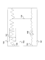
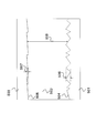
- FIG. 1 shows a sectional view of an example of a conventional gate insulating film.
- a commercial product of a silicon wafer provided with a semiconductor layer 101 made of silicon (Si) having a surface with a (100) plane orientation was prepared.
- the surface of the semiconductor layer 101 of the silicon wafer as it was purchased was cleaned by a normal semiconductor cleaning method, and then the surface of the semiconductor layer 1 cleaned at 400 ° C. was subjected to radical oxidation (by radical oxygen formed in plasma).
- the gate insulating film 102 having an average thickness of 6 nm was formed by oxidation by directly oxidizing the silicon surface.
- an electrode 103 was formed on the gate insulating film 102 by an electrode forming technique used in a normal semiconductor field.
- the interface 104 between the semiconductor layer 101 and the gate insulating film 102 is referred to as “semiconductor layer side interface 104”, and the interface 105 between the gate insulating film 102 and electrode 103 is referred to as “electrode side interface”. 105 ".
- the sizes of the unevenness 106 on the semiconductor layer side interface 104 and the unevenness 107 on the electrode side interface 105 were measured.
- the maximum value of the unevenness in an arbitrary region having a length (L) of 1 ⁇ m along the extending direction of the insulating film 102 (left and right direction of the paper surface) is displayed as a peak-to-valley.
- the unevenness 106 of the semiconductor layer side interface 104 was 0.9 nm
- the unevenness 107 of the electrode side interface 105 was 1.2 nm.
- the present inventors obtained the following new knowledge. According to the knowledge, the size of the unevenness on the surface of the semiconductor layer before oxidation appears almost as it is as the size of the unevenness of the interface 105 between the oxide film (insulating film) 102 and the electrode 103.
- the size of the irregularities at the interface 104 between the semiconductor layer 101 and the oxide film 102 becomes smaller than the size of the irregularities on the surface of the semiconductor layer before oxidation, and the degree of the irregularities is relaxed.
- the size of the unevenness 107 on the electrode side interface 105 substantially reflects the size of the unevenness on the surface of the semiconductor layer 101 before oxidation, and the unevenness 106 on the semiconductor layer side interface 104 undergoes a radical oxidation process. As a result, the original size is relaxed to form small irregularities as shown in the figure.
- this effect can also be obtained by thermal oxidation. That is, if the surface flatness (average roughness) Ra of the original semiconductor layer is greater than 0.1 nm, the unevenness tends to be reduced even by thermal oxidation. However, in radical oxidation, the tendency for the size of the concavities and convexities to be smaller is more pronounced than in thermal oxidation.
- the interface unevenness is larger than the original unevenness in the thermal oxidation, but the radical oxidation does not substantially change.
- the (average) film of the gate insulating film 102 If the thickness 118 is 6 nm, the size of the interface irregularity occupies a ratio of 15% to 20% of the (average) film thickness 118 of the gate insulating film 102.
- the film thickness of the gate insulating film is being reduced to improve the low-voltage driving and the switching speed of the formed transistor at present, and this trend is said to continue in the future.
- a MOS transistor having a gate insulating film having a thickness of 2 nm has also been proposed.
- the size of the interface unevenness reaches 45% to 60% of the thickness of the gate insulating film.
- the reason why the film thickness of the film thickness 118 is described as “average film thickness” is that the semiconductor layer side interface 104 and the electrode side interface 105 of the gate insulating film 102 are irregularly uneven. Since the measured value of the film thickness is location-dependent, the average value of a plurality of measured values within the range of the length (L) of the gate insulating film 102 is handled as the film thickness of the gate insulating film 102 for convenience in the present invention. Because.
- the aerial surface on the semiconductor layer 1 side of the gate insulating film 102 expressed by the average film thickness is denoted as “first principal surface”, and the aerial surface on the electrode 103 side is denoted as “second principal surface”.
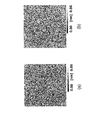
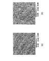
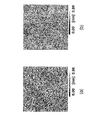
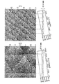
- 2 (a) and 2 (b) show examples of atomic force microscope images (examples of FIG. 1) of the electrode side interface and the semiconductor layer side interface, respectively.
- the electrode side interface is 0.09 nm and the semiconductor layer side interface is 0.12 nm.
- Z (x, y), ZAve, and A indicate the height, average height, and number of measurement points at position (x, y), respectively.
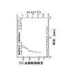
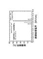
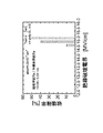
- 3 and 4 show the relationship between the breakdown electric field and the breakdown probability of the gate insulating film made of a silicon oxide film having a thickness of 6 nm formed by radical oxidation using oxygen radicals at 400 ° C., and the gate insulating film.
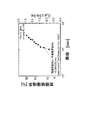
- An example of the cumulative probability of lifetime when applying a constant current stress of +0.1 A / cm 2 (example of the gate insulating film in FIG. 1) is shown.
- the present inventors have found that the breakdown electric field strength of the gate insulating film is low, the lifetime of the gate insulating film when a constant current stress is applied is short, or that the experimental values vary. We believe that this is due to the above. According to the data shown in FIG. 3, 30% of the gate insulating film breaks when the dielectric breakdown electric field is 13.5 MV / cm or less.
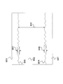
- FIG. 5 shows a schematic cross-sectional view of another example of a conventional gate insulating film.
- the surface of the semiconductor layer 501 made of Si having a (100) plane orientation is annealed at a high temperature in an Ar atmosphere at a high temperature to flatten the surface to the minimum level difference between atoms, and then heat is applied.
- a thickness of 6 nm was formed by oxidation (moisture oxidation).
- the insulating film 502 has a semiconductor layer side interface 504 between the semiconductor layer 501 and an electrode side interface 505 between the semiconductor layer 501 and the gate electrode 503 on the side opposite to the semiconductor layer 501.
- the size of the unevenness 506 of the semiconductor layer side interface 504 and the size of the unevenness 507 of the electrode side interface 505 are 0.8 nm and 0.14 nm, respectively, in the region of 1 ⁇ m length according to the above definition.
- the unevenness 507 of the electrode-side interface 505 remains the smallest step between Si atoms, reflecting the flatness of the silicon surface before oxidation (the original surface of the semiconductor layer 502).
- the irregularities 506 of the semiconductor layer side interface 504 are enlarged by thermal oxidation.
- the average film thickness 518 of the gate insulating film 502 is 6 nm
- the size of the unevenness 506 of the semiconductor layer side interface 504 is 13.3% of the average film thickness 518 of the gate insulating film.
- the size of the unevenness 507 on the electrode-side interface 505 is the size of the smallest step between Si atoms whose plane orientation is the (100) plane, which is 2.3% of the average film thickness 518 of the gate insulating film 502. is there.
- FIGS. 6A and 6B show another example of atomic force microscope images of the electrode side interface and the semiconductor layer side interface, respectively.
- the average roughness Ra is 0.08 nm and 0.04 nm at the electrode side interface and the semiconductor layer side interface, respectively.
- the lower limit value of the average roughness Ra measured with an atomic force microscope is determined by the noise signal intensity of the measuring instrument, and the value is currently about 0.04 nm. That is, in practice, even if an interface having an average roughness Ra of less than 0.04 nm is measured, Ra measured by an atomic force microscope is about 0.04 nm.
- FIG. 7 and 8 show the relationship between the breakdown electric field and the breakdown probability of the gate insulating film made of a silicon oxide film having a thickness of 6 nm formed by moisture oxidation at 750 ° C., and +0.1 A / cm for the gate insulating film.
- Another example of the cumulative probability of life when a constant current stress of 2 is applied (example of the gate insulating film shown in FIG. 5) is shown.
- the size of the unevenness 507 of the tail electrode side interface 505 is the size of the smallest step between the silicon (Si) atoms when the surface orientation of the surface of the semiconductor layer 501 is the (100) plane.
- the size of the unevenness 506 of the semiconductor side interface 504 is larger than 10% of the film thickness of the insulating film 502, electric field concentration occurs locally due to the size of the unevenness 506 of the semiconductor layer side interface 504, and the electric field strength. It seems that there is a place where becomes locally high.
- the breakdown electric field strength of the gate insulating film is low, the life of the gate insulating film when a constant current stress is applied is short, or the measured values vary. It is done.
- the present invention has been made in view of the findings of the review as described above.
- One of the main requirements of the present invention is that the size of the irregularities at both interfaces of the gate insulating film of an electronic element such as a transistor is 10% or less of the thickness of the gate insulating film.
- the gate insulating film to be formed is defined by the length (left and right direction of the paper surface in the example of FIG. 1) and the width (depth direction of the paper surface in the example of FIG. 1).
- the size of all irregularities in the surface (electrode side interface) of the gate insulating film and the size of all irregularities in the back surface (semiconductor layer side interface) are 10% or less of the average thickness of the gate insulating film. This is a feature of the present invention.
- the size of the unevenness at both interfaces is the size of the minimum step between atoms in the plane orientation of the semiconductor layer.
- FIG. 21 shows the measurement results of the average roughness Ra of the Si semiconductor layer surface before oxidation and the average roughness Ra of the insulating film / semiconductor layer interface (semiconductor layer side interface) described above.
- the average roughness Ra of the surface of the Si semiconductor layer before oxidation is substantially equal to the average roughness Ra at the interface between the insulating film and the electrode (electrode-side interface) as described above.
- FIG. 21 shows a case where an insulating film having a thickness of 6 nm in terms of a silicon oxide film is formed by oxygen radical oxidation and a case where it is formed by moisture oxidation (thermal oxidation using moisture). ing. In these oxidation examples, both were performed at 400 ° C. and 750 ° C.
- the average roughness Ra of the surface of the Si semiconductor layer before oxidation exceeds 0.10 nm
- the average roughness Ra of the insulating film / Si semiconductor layer interface semiconductor layer side interface
- the average roughness Ra of the semiconductor layer surface is considerably relaxed.
- the insulating film / Si semiconductor layer interface (semiconductor layer) It can be seen that the average roughness Ra of the side interface is rougher than the average roughness Ra of the surface of the original Si semiconductor layer before oxidation.
- the average roughness Ra of the insulating film / Si semiconductor layer interface is the average of the surface of the original Si semiconductor layer before oxidation. It turns out that it is relieved rather than roughness Ra.
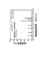
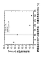
- FIG. 22 shows the relationship between the dielectric breakdown electric field (MV / cm) and the ratio (%) of the unevenness at the electrode side interface and the size of the unevenness at the semiconductor layer side interface to the film thickness of the insulating film.
- the ratio (%) of the unevenness at the semiconductor side interface and the unevenness at the electrode side interface to the film thickness of the gate insulating film exceeds 10% and reaches 20%, the minimum value of the dielectric breakdown electric field is reached. Is 12.5 MV / cm. When it becomes 30%, it is 12.5 MV / cm or less.
- the minimum value of the dielectric breakdown electric field is from 14.25 MV / cm to 14.4 MV / cm. It has reached 75 MV / cm (high withstand voltage). From this point, it can be seen that the dielectric breakdown electric field value changes significantly significantly when the ratio (%) of the unevenness at the semiconductor side interface and the unevenness at the electrode side interface to the film thickness of the gate insulating film is 10%.
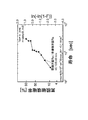
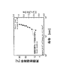
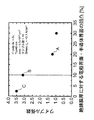
- FIG. 23 shows the ratio (%) of the unevenness at the semiconductor side interface and the unevenness at the electrode side interface to the film thickness of the gate insulating film (insulating film area is 4.0 ⁇ 10 ⁇ 2 cm 2 ), and the constant of the gate insulating film.
- the relationship with the Weibull coefficient extracted from the range in which the cumulative probability of life when applying stress current +0.1 A / cm 2 is 40% or less is shown.
- the Weibull coefficient is an index indicating the variation in life to dielectric breakdown, and the smaller the value, the higher the probability of failure in the range where the variation is large and the lifetime to dielectric breakdown is short.
- the Weibull coefficient of the example shown in FIG. 4 is indicated by a point A
- the Weibull coefficient of the example shown in FIG. 12 is indicated by a point B
- the example of FIG. The Weibull coefficient is indicated by point C.
- the Weibull coefficient is as low as about 1 or less.
- the Weibull coefficient rapidly increases to 3 or more.
- the semiconductor layer may be any of single crystal, polycrystal, and amorphous, and its constituent materials are Si (silicon), SiGe x (silicon germanium) (0 ⁇ x ⁇ 1), Ge (germanium). , GaAs (gallium arsenide), GaN (gallium nitride), SiC (silicon carbide), InP (indium phosphorus), and other semiconductor materials.
- the method for manufacturing a gate insulating film according to the present invention is a method for manufacturing a gate insulating film in which an insulating film that contacts the semiconductor layer is formed on the semiconductor layer, and an electrode layer is formed by directly contacting the semiconductor layer.
- the manufacturing process includes at least one planarization treatment step for reducing the thickness of the semiconductor layer surface to 10% or less of the thickness of the insulating film forming the unevenness.
- the surface of the semiconductor layer is oxidized, oxynitrided or nitrided so that the size of the irregularities at the semiconductor layer side interface to be formed is 10% or less of the thickness of the insulating film to be formed.
- An insulating film is formed on the substrate.
- an insulating film (insulating oxide film) is formed by oxidizing the surface of the semiconductor layer in moisture or oxygen at a temperature of 900 ° C. or higher, or in a mixed atmosphere of moisture and oxygen, and then the insulating film A step of removing a portion unnecessary for the electronic element formed by using a chemical solution containing hydrofluoric acid may be included.
- the atmosphere is any one of Ar (argon), H 2 (hydrogen), and Ar / H 2 (argon / hydrogen) at 800 ° C. or higher.
- Ar argon
- H 2 hydrogen
- Ar / H 2 argon / hydrogen
- the insulating film forming step is preferably an isotropic oxidation, oxynitridation or nitriding treatment step in which the film formation rate does not depend on a difference in plane orientation of the semiconductor layer, for example, an oxidation treatment step using oxygen radicals, a nitrogen radical It is preferable to include a nitriding treatment process using oxynitriding or an oxynitriding treatment process using a mixed radical of oxygen radicals and nitrogen radicals or NH radicals.
- the insulating film forming step includes any one of Hf (hafnium), La (lanthanum), Ti (titanium), Al (aluminum), O (oxygen), Si (silicon), Pr (praseodymium), and N (nitrogen).
- a film forming step of depositing an insulating film including the above may be included.
- the MOS transistor according to the present invention includes a semiconductor layer, a gate insulating film provided directly on the semiconductor layer, and a gate electrode layer provided directly on the insulating film, and the semiconductor layer and the gate insulating film
- the size of all irregularities at the interface with the film and the size of all irregularities at the interface between the gate insulating film and the gate electrode layer are the length in a direction parallel to the extending direction of the gate insulating film. In the length of 1 ⁇ m in an arbitrary region, the smaller the film thickness of the gate insulating film is, the smaller it is depending on the thickness.
- the channel polarity may be n-type or p-type.
- All the MOS transistors in the CMOS circuit according to the present invention have the same configuration as the above MOS transistors.
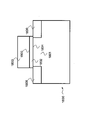
- FIG. 9 shows a schematic sectional view of a gate insulating film according to a first embodiment of the present invention.
- FIGS. 10A and 10B show atomic force microscope images of the semiconductor layer side interface of the gate insulating film and the surface of the gate insulating film (surface opposite to the semiconductor layer side interface).
- FIG. 10 shows the average roughness Ra
- FIG. 11 shows the relationship between the breakdown electric field strength and the breakdown probability of the gate insulating film whose gate insulating film area (stacked surface area) is 4.0 ⁇ 10 ⁇ 2 cm 2. It is.
- FIG. 12 shows the cumulative probability of life when a constant stress current +0.1 A / cm 2 is applied to a gate insulating film whose gate insulating film area is 4.0 ⁇ 10 ⁇ 2 cm 2 .
- a semiconductor substrate having an Si semiconductor layer 901 was prepared.
- silicon (Si) is used as the semiconductor layer 901.
- a semiconductor layer 901 is formed on the surface of a Si wafer by an epitaxial method, and the surface orientation of the surface of the semiconductor layer 901 is a (100) plane.
- the semiconductor layer 901 was n-type and had a resistivity of 10 ⁇ ⁇ cm.
- the resistivity of the semiconductor layer 901 is preferably 8 to 12 ⁇ ⁇ cm.
- the substrate provided with the semiconductor layer 901 was also n-type, and its resistivity was 0.01 ⁇ ⁇ cm.
- the resistivity of the substrate is desirably 0.008 to 0.012 ⁇ ⁇ cm.
- the polarity of the semiconductor layer 901 may be p-type, or may be manufactured by the Cz method or the FZ method. Further, the plane orientation of the semiconductor layer 901 is not limited to the (100) plane.
- an oxide film having a thickness of 1 ⁇ m was formed on the surface of the semiconductor layer 901 at a temperature of 1000 ° C. in a mixed atmosphere of moisture and oxygen.
- the formed oxide film was removed using a mixed chemical solution of hydrochloric acid and hydrofluoric acid.
- the (100) surface of the semiconductor layer 901 has an average roughness of 0.06 nm.
- the maximum size of the irregularities in the region having a length of 1 ⁇ m in the direction parallel to the surface was 0.6 nm.
- the planarization treatment as a part of the planarization treatment, it is preferable to use a method of immersing a semiconductor substrate in a dilute hydrofluoric acid chemical solution in an environment where light is blocked and the dissolved oxygen concentration of the chemical solution is 1 ppb or less. It is an aspect.
- the surface of the semiconductor layer 901 having an average roughness of 0.06 nm formed as described above was oxidized by an oxygen radical method to form a gate insulating film 902.
- the gate insulating film 902 was formed using an oxidation method using oxygen radicals as oxidizing species using a microwave-excited high-density plasma apparatus.
- the formed gate insulating film 902 has a thickness of 6.0 nm.
- the largest unevenness in the unevenness 906 of the semiconductor layer side interface 904 was 10% of the average film thickness of the gate insulating film 902.
- a gate electrode 903 was formed on the surface of the gate insulating film 902 as follows.
- an amorphous Si film doped with about 3 ⁇ 10 20 cm ⁇ 3 of P (phosphorus) to a thickness of 150 nm is formed on the gate insulating film 902 by using a low pressure chemical vapor deposition method.
- P (phosphorus) was activated and the amorphous Si film could be converted into n + type polycrystalline Si.
- n + type polycrystalline Si film In the present invention, after forming a non-doped amorphous Si film, P (phosphorus) ions are implanted into the amorphous Si film, and then the P (phosphorus) ions are activated to form an n + type polycrystalline Si film. May be used. In this way, a gate electrode 903 of n + type polycrystalline Si was formed.
- the polarity of the gate electrode is not limited to n + type, but may be p + type.
- the gate electrode 903 may be made of a metal such as Ti (titanium), Ta (tantalum), W (tungsten), Al (aluminum), or a conductive nitride such as TiN (titanium nitride) or TaN (tantalum nitride). Good.
- the gate electrode 903 was patterned so that the surface thereof had an area of 4.0 ⁇ 10 ⁇ 2 cm 2 .
- the breakdown voltage characteristics of the gate insulating film 903 thus prepared were measured.
- FIG. 11 shows the relationship between the breakdown electric field strength and the breakdown probability at that time. According to FIG. 11, it can be seen that the breakdown probability is small (zero) in the range where the dielectric breakdown electric field strength is small (that is, the range of 14.0 MV / cm or less).
- FIG. 12 shows the cumulative probability of life when a constant stress current + 0.1 A / cm 2 is applied.
- the range life is small (i.e., less than the range of 10 3 seconds) it can be seen cumulative fracture probability is small.
- FIG. 13 shows a schematic cross-sectional view of a gate insulating film according to a second embodiment of the present invention.
- 14A and 14B show an atomic force microscope image and a surface height profile of the surface of the semiconductor layer after the planarization step.
- FIG. 15A shows an atomic force microscope image and average roughness Ra of the gate insulating film on the semiconductor layer side interface
- FIG. 15B shows an atomic force microscope image of the surface of the gate insulating film. And the average roughness Ra is indicated.
- FIG. 16 shows the relationship between the breakdown field strength of the formed gate insulating film and the breakdown probability.
- FIG. 17 shows the cumulative probability of life when a constant stress current +0.1 A / cm 2 is applied to the formed gate insulating film.
- the same semiconductor substrate as that in the first embodiment was used.
- the semiconductor layer was n-type and had a resistivity of 10 ⁇ ⁇ cm.
- the substrate on which the n-type semiconductor layer was formed was an n-type Si substrate, and its resistivity was 0.01 ⁇ ⁇ cm.
- a surface flattening process was performed to make the unevenness of the Si semiconductor layer surface preferably the size of the minimum step between atoms in the plane orientation (100) plane of the surface of the Si substrate.
- the natural oxide film on the surface of the Si semiconductor layer was removed with a dilute hydrofluoric acid chemical solution, and then heat treatment was performed in a high-clean Ar atmosphere under atmospheric pressure to flatten the surface of the Si semiconductor layer.
- the heat treatment condition was 900 ° C. for 1 hour.
- the atmosphere during the heat treatment during the planarization treatment may be H 2 (hydrogen) or Ar / H 2 (argon / hydrogen). Further, the pressure during the heat treatment may be lower than the atmospheric pressure.
- the surface of the (100) plane of the Si semiconductor layer is planarized at the atomic level.
- the average roughness Ra measured by the atomic force microscope is 0.04 nm, which is the measurement noise level of the atomic force microscope as described above.
- the unevenness in the region having a length of 1 ⁇ m in the direction parallel to the surface is the size of the smallest step between atoms on the Si semiconductor layer (100) surface, as is apparent from FIGS. 14 (a) and 14 (b). It is 0.14 nm.
- an oxide insulating film is formed on the Si semiconductor layer whose surface is planarized at the atomic level as described above, using an oxidation method using oxygen radicals as an oxidizing species using a microwave-excited high-density plasma apparatus. Then, a gate insulating film was formed. At this time, the thickness of the gate insulating film was 6 nm.
- the size of the unevenness at the interface between the Si semiconductor layer and the formed gate insulating film (see FIG. 15A) and the average roughness Ra when the surface of the formed gate insulating film is observed with an atomic force microscope are: It was confirmed that it was maintained at 0.04 nm (see FIG. 15B).
- FIG. 16 shows the relationship between the breakdown field strength of the patterned gate insulating film and the breakdown probability. As shown in FIG. 16, it can be seen that the breakdown probability is low (zero) in a range where the breakdown electric field strength is small (ie, a range of 14.5 MV / cm or less).
- FIG. 17 shows the cumulative probability of the lifetime of the patterned gate insulating film when a constant stress current + 0.1 A / cm 2 is applied. According to FIG. 17, it can be seen that the cumulative failure probability in the range where the lifetime is small (the range of 2 ⁇ 10 3 seconds or less) is small.
- FIG. 18 shows a cross-sectional structure of a MOS transistor according to a third embodiment of the present invention.
- the n-type channel MOS transistor including the gate insulating film described in the first or second embodiment is described, but a p-type channel MOS transistor may be used.
- B boron
- a gate electrode 1803 is formed over the gate insulating film 1802, and an interface 1805 is formed between the gate insulating film 1802 and the gate electrode 1803.
- the average roughness of the interface 1804 between the semiconductor layer 1801 and the gate insulating film 1802 is directly reflected in the average roughness on the surface of the gate insulating film 1802. .
- ion implantation of As (arsenic) ions was performed under the conditions of 20 keV and 2 ⁇ 10 15 cm ⁇ 2 in order to form the source region 1808 and the drain region 1809. Thereafter, annealing was performed at a temperature of 1000 ° C. for 5 seconds to activate As (arsenic) ions.
- the ion implantation conditions may be adjusted in order to make the depths of the n + layers of the source region and drain region to be created a target depth.
- the ion species to be implanted may be cluster ions including As (arsenic). Further, the ion species to be implanted may be P (phosphorus) ions.
- the MOS transistor according to the present embodiment had the same effects as those of the first or second embodiment with respect to the dielectric breakdown electric field and life of the gate insulating film.
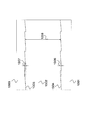
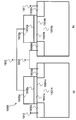
- FIG. 19 shows a schematic sectional view of a CMOS circuit according to a fourth embodiment of the present invention.
- a CMOS circuit 1900 shown in FIG. 19 includes an n-type channel MOS transistor (left side transistor: “FIG. 19A”) and a p-type channel MOS transistor (right side transistor: “(b) in FIG. 19” described in the third embodiment. ) ”) CMOS inverter circuit consisting of series connection.
- the source region 1908a of the n-type MOS transistor (a) is connected to the ground terminal 1910.
- the source region 1908b of the p-type MOS transistor (b) is connected to the power supply terminal 1911b.
- the gate and electrode 1903a of the p-type MOS transistor (a) and the gate electrode 1903b of the p-type MOS transistor (b) are both connected to the input terminal 1912.
- the drain regions 1909a and 1909b are both connected to the output terminal 1913.
- the gate insulating film 1902a of the n-type MOS transistor, the gate insulating film 1902b of the p-type MOS transistor, and the interfaces 1904a, 1904b, 1905a, and 1905b were formed in the same manner as in the third embodiment.
- the CMOS circuit according to the present embodiment had the same effects as those of the first or second embodiment with respect to the dielectric breakdown electric field and the lifetime of the gate insulating film.
- FIG. 20 shows a schematic sectional view of a semiconductor memory composed of a floating gate type transistor according to a fifth embodiment of the present invention.
- the configuration of the gate insulating film 2002 and the floating gate electrode 2014 is the same as that of the n-type channel MOS transistor described in the third embodiment.
- the semiconductor memory 2000 has a structure in which an interelectrode insulating film 2015 and a control gate electrode 2016 are sequentially stacked on a floating gate electrode 2014. Further, a source region 2008 and a drain region 2009 are also provided.
- the semiconductor memory 2000 according to the present embodiment had the same effects as those of the first or second embodiment with respect to the dielectric breakdown electric field and the lifetime of the gate insulating film.
- the variation in current flowing from the source region 2008 to the drain region 2009 via the gate insulating film 2002 during writing was suppressed.
- the reason is considered to be that variation in the electric field applied to the gate insulating film 2002 is suppressed.
- the semiconductor memory 2000 floating gate type transistor
- the semiconductor memory 2000 floating gate type transistor according to the fifth embodiment is a highly reliable semiconductor memory in which writing failures and reading failures are suppressed.
- the present invention can be applied to an insulating film, a MOS capacitor, a MOS transistor, a CMOS circuit or a semiconductor memory circuit employing at least one of these, and a manufacturing method thereof.
Landscapes
- Insulated Gate Type Field-Effect Transistor (AREA)
- Formation Of Insulating Films (AREA)
- Electrodes Of Semiconductors (AREA)
- Non-Volatile Memory (AREA)
- Chemical & Material Sciences (AREA)
- Chemical Kinetics & Catalysis (AREA)
- General Chemical & Material Sciences (AREA)
Abstract
Description
前記半導体層と界面で形成して接触する絶縁膜と、
前記絶縁膜と前記半導体層とは反対側で界面を形成して接触する電極層とを有し、
前記半導体層と前記絶縁膜の界面における凹凸が、前記絶縁膜と前記電極層との界面における凹凸にそのまま反映されるように、前記絶縁膜の厚さ及び前記両界面の凹凸が形成されていることを特徴とする半導体装置にある。

本発明は上記のような見直しによる知見に鑑みてなされたものである。
これらの酸化の例では、何れも400℃と750℃で行った。
絶縁破壊電圧値は測定したものの中の最小値のものを採用した。
本発明の第1実施形態に係るゲート絶縁膜の模式的断面図を図9に示す。
ここでは、シリコン(Si)を半導体層901として用いた。この半導体基板は、Siウエファーの表面にエピタキシャル法によって半導体層901が形成されたもので、半導体層901表面の面方位は(100)面である。
半導体層901はn型で抵抗率は、10Ω・cmであった。
また、半導体層901の面方位は(100)面に限らない。
次いで、半導体層901の表面を酸化処理して絶縁性酸化膜を形成した。
この様にして、n+型多結晶Siのゲート電極903を形成した。
このようにして作成したゲート絶縁膜903の耐圧特性を測定した。
本発明の第2実施形態に係るゲート絶縁膜の模式的断面図を図13に示す。
半導体層はn型でその抵抗率は10 Ω・cmであった。
熱処理条件は、900℃で1時間であった。
また、熱処理中の圧力は、大気圧よりも低圧としてもよい。
この際のゲート絶縁膜の膜厚は6nmであった。
パターニングされたゲート絶縁膜の絶縁破壊電界強度と破壊確率との関係を図16に示す。図16に示されているように、絶縁破壊電界強度が小さい範囲(即ち、14.5MV/cm以下の範囲)における破壊確率が小さい(ゼロである)ことが分かる。
本発明の第3実施形態に係るMOSトランジスタの断面構造図を図18に示す。ここでは、第1あるいは第2実施形態で説明したゲート絶縁膜を備えているn型チャネルMOSトランジスタについて記載するが、p型チャネルMOSトランジスタであってもよい。
本発明の第4実施形態に係るCMOS回路の模式的断面構造図を図19に示す。
本発明の第5実施形態に係るフローティングゲート型トランジスタからなる半導体メモリの模式的断面図を図20に示す。
更にソース領域2008、ドレイン領域2009をも備えている。
102,502,902,1302,1802,1902a,1902b・・・ゲート絶縁膜
103,503,903,1303,1803,1903a,1903b・・・ゲート電極
104,504,904,1304,1804,1904a,1904b・・・半導体層側界面
105,505,905,1305,1805,1905a,1905b・・・電極側界面
106,506,906,1306・・・・・・半導体層側界面の凹凸
107,507,907,1307・・・・・・電極側界面の凹凸
118,518,918,1318・・・・・・ゲート絶縁膜の膜厚
1800・・・・・・n型チャネルMOSトランジスタ
1808・・・・・・ソース領域
1809・・・・・・ドレイン領域
1900・・・・・・CMOSインバーター回路
1910・・・・・・グラウンド端子
1911・・・・・・電源端子
1912・・・・・・入力端子
1913・・・・・・出力端子
2000・・・・・・半導体メモリ
2014・・・・・・フローティングゲート電極
2015・・・・・・電極間絶縁膜
2016・・・・・・制御ゲート電極
Claims (8)
- 半導体層と、
前記半導体層と界面で形成して接触する絶縁膜と、
前記絶縁膜と前記半導体層とは反対側で界面を形成して接触する電極層と
を有し、
前記半導体層と前記絶縁膜との界面の凹凸の大きさと、前記絶縁膜と前記電極層との界面の凹凸の大きさとが、それぞれ、前記絶縁膜の延在する方向に平行な方向の長さ1μmの領域において、前記絶縁膜の厚さが小さいほどその小ささに対応した小ささであることを特徴とする半導体装置。 - 前記半導体層と前記絶縁膜との界面の凹凸の大きさが前記絶縁膜の厚さの10%以下で、かつ前記絶縁膜と前記電極層との界面の凹凸の大きさが前記絶縁膜の厚さの10%以下であることを特徴とする請求項1に記載の半導体装置。
- 前記両界面の凹凸が、それぞれ前記半導体層の面方位における原子間の最小の段差であることを特徴とする請求項1又は2に記載の半導体装置。
- 半導体層と、
該半導体層上に直に接触している絶縁膜と、
前記半導体層とは反対側で前記絶縁膜と直に接触している電極と、
を有する半導体装置の製造方法であって、
該製造方法の工程中に、
用意した半導体層の表面の凹凸の大きさを、形成される絶縁膜の厚さの10%以下にするための平坦化工程と、
前記半導体層と前記絶縁膜の接する界面の凹凸の大きさと絶縁膜の前記電極を設ける表面の凹凸の大きさがそれぞれ前記形成する絶縁膜の厚さの10%以下になるような酸化、酸窒化または窒化方法によって前記絶縁膜を形成する絶縁膜形成工程と、
を含むことを特徴とする半導体装置の製造方法。 - 前記平坦化工程が、
前記半導体層表面の凹凸を、前記半導体層の面方位における原子間の最小の段差にするための平坦化工程を含み、
前記絶縁膜形成工程が、
前記半導体層と前記絶縁膜の接する界面の凹凸の大きさと絶縁膜の前記電極を設ける表面の凹凸の大きさがそれぞれ前記段差の大きさと同等乃至は実質的に同等となるように、酸化、酸窒化または窒化方法によって絶縁膜を形成する工程を含む
請求項4に記載の半導体装置の製造方法。 - 前記平坦化工程は、
水分または酸素の雰囲気、または水分と酸素の混合した雰囲気下において900℃以上の温度で前記用意した半導体層上に酸化膜を形成し、該形成した酸化膜を、フッ酸を含む薬液を用いて除去する工程
を含む請求項4に記載の半導体装置の製造方法。 - 前記平坦化工程は、
前記用意した半導体層は、その表面の自然酸化膜を除去した後に、Ar,H2,Ar/H2のいずれかの雰囲気中において800℃以上の温度で熱処理する工程を含むこと請求項4に記載の半導体装置の製造方法。 - 半導体層と、
該半導体層と直に接触している絶縁膜と、
該絶縁膜と前記半導体層とは反対側で直に接触している電極とを有し、
前記半導体層と前記絶縁膜の界面の凹凸の大きさが、前記絶縁膜と前記電極との界面の凹凸の大きさに反映されるように、前記絶縁膜の厚さ及び前記両界面の凹凸が形成されていることを特徴とする半導体装置。
Priority Applications (2)
| Application Number | Priority Date | Filing Date | Title |
|---|---|---|---|
| KR1020147016106A KR20140090684A (ko) | 2011-11-17 | 2012-11-16 | 반도체 장치 및 그 제조 방법 |
| US14/356,666 US9153658B2 (en) | 2011-11-17 | 2012-11-16 | Semiconductor device and method of manufacturing the same |
Applications Claiming Priority (2)
| Application Number | Priority Date | Filing Date | Title |
|---|---|---|---|
| JP2011-251556 | 2011-11-17 | ||
| JP2011251556 | 2011-11-17 |
Publications (1)
| Publication Number | Publication Date |
|---|---|
| WO2013073671A1 true WO2013073671A1 (ja) | 2013-05-23 |
Family
ID=48429724
Family Applications (1)
| Application Number | Title | Priority Date | Filing Date |
|---|---|---|---|
| PCT/JP2012/079799 Ceased WO2013073671A1 (ja) | 2011-11-17 | 2012-11-16 | 半導体装置及びその製造方法 |
Country Status (4)
| Country | Link |
|---|---|
| US (1) | US9153658B2 (ja) |
| JP (1) | JPWO2013073671A1 (ja) |
| KR (1) | KR20140090684A (ja) |
| WO (1) | WO2013073671A1 (ja) |
Cited By (1)
| Publication number | Priority date | Publication date | Assignee | Title |
|---|---|---|---|---|
| JP2016058500A (ja) * | 2014-09-08 | 2016-04-21 | 国立大学法人東北大学 | 半導体素子の形成方法 |
Families Citing this family (2)
| Publication number | Priority date | Publication date | Assignee | Title |
|---|---|---|---|---|
| KR20140090684A (ko) * | 2011-11-17 | 2014-07-17 | 고쿠리츠다이가쿠호진 도호쿠다이가쿠 | 반도체 장치 및 그 제조 방법 |
| US9922161B2 (en) * | 2013-02-27 | 2018-03-20 | The Regents Of The University Of California | IC layout adjustment method and tool for improving dielectric reliability at interconnects |
Citations (5)
| Publication number | Priority date | Publication date | Assignee | Title |
|---|---|---|---|---|
| JPH11111674A (ja) * | 1997-09-30 | 1999-04-23 | Shin Etsu Handotai Co Ltd | シリコンウエーハの表面粗さを改善する方法および表面粗さを改善したシリコンウエーハ |
| JP2005093562A (ja) * | 2003-09-12 | 2005-04-07 | Tadahiro Omi | 半導体装置の製造方法 |
| JP2010045204A (ja) * | 2008-08-13 | 2010-02-25 | Hikari Kobayashi | 半導体基板、半導体装置およびその製造方法 |
| JP2010050230A (ja) * | 2008-08-20 | 2010-03-04 | Shin Etsu Handotai Co Ltd | シリコンウェーハの製造方法及びシリコンウェーハ |
| WO2011096417A1 (ja) * | 2010-02-04 | 2011-08-11 | 国立大学法人東北大学 | シリコンウェーハおよび半導体装置 |
Family Cites Families (14)
| Publication number | Priority date | Publication date | Assignee | Title |
|---|---|---|---|---|
| JP3981426B2 (ja) * | 1996-07-12 | 2007-09-26 | シャープ株式会社 | ゲート絶縁膜形成方法 |
| US8026161B2 (en) * | 2001-08-30 | 2011-09-27 | Micron Technology, Inc. | Highly reliable amorphous high-K gate oxide ZrO2 |
| US6953730B2 (en) * | 2001-12-20 | 2005-10-11 | Micron Technology, Inc. | Low-temperature grown high quality ultra-thin CoTiO3 gate dielectrics |
| US7179746B2 (en) * | 2002-12-02 | 2007-02-20 | Foundation fõr Advancement of Internati{dot over (o)}nal Science | Method of surface treatment for manufacturing semiconductor device |
| US6723666B1 (en) * | 2003-03-06 | 2004-04-20 | Advanced Micro Devices, Inc. | Method for reducing gate oxide surface irregularities |
| JP2004356114A (ja) * | 2003-05-26 | 2004-12-16 | Tadahiro Omi | Pチャネルパワーmis電界効果トランジスタおよびスイッチング回路 |
| CN100524822C (zh) * | 2004-04-09 | 2009-08-05 | 东京毅力科创株式会社 | 栅极绝缘膜的形成方法 |
| US7544596B2 (en) * | 2005-08-30 | 2009-06-09 | Micron Technology, Inc. | Atomic layer deposition of GdScO3 films as gate dielectrics |
| WO2008007748A1 (en) * | 2006-07-13 | 2008-01-17 | National University Corporation Tohoku University | Semiconductor device |
| US7601648B2 (en) * | 2006-07-31 | 2009-10-13 | Applied Materials, Inc. | Method for fabricating an integrated gate dielectric layer for field effect transistors |
| JP2008109014A (ja) * | 2006-10-27 | 2008-05-08 | Covalent Materials Corp | 半導体ウェーハおよびその製造方法 |
| US8445386B2 (en) * | 2010-05-27 | 2013-05-21 | Cree, Inc. | Smoothing method for semiconductor material and wafers produced by same |
| WO2012169462A1 (ja) * | 2011-06-07 | 2012-12-13 | 国立大学法人東北大学 | フォトダイオード及びその製造方法、フォトダイオードアレイ、分光光度計、並びに固体撮像装置 |
| KR20140090684A (ko) * | 2011-11-17 | 2014-07-17 | 고쿠리츠다이가쿠호진 도호쿠다이가쿠 | 반도체 장치 및 그 제조 방법 |
-
2012
- 2012-11-16 KR KR1020147016106A patent/KR20140090684A/ko not_active Withdrawn
- 2012-11-16 JP JP2013544342A patent/JPWO2013073671A1/ja active Pending
- 2012-11-16 US US14/356,666 patent/US9153658B2/en active Active
- 2012-11-16 WO PCT/JP2012/079799 patent/WO2013073671A1/ja not_active Ceased
Patent Citations (5)
| Publication number | Priority date | Publication date | Assignee | Title |
|---|---|---|---|---|
| JPH11111674A (ja) * | 1997-09-30 | 1999-04-23 | Shin Etsu Handotai Co Ltd | シリコンウエーハの表面粗さを改善する方法および表面粗さを改善したシリコンウエーハ |
| JP2005093562A (ja) * | 2003-09-12 | 2005-04-07 | Tadahiro Omi | 半導体装置の製造方法 |
| JP2010045204A (ja) * | 2008-08-13 | 2010-02-25 | Hikari Kobayashi | 半導体基板、半導体装置およびその製造方法 |
| JP2010050230A (ja) * | 2008-08-20 | 2010-03-04 | Shin Etsu Handotai Co Ltd | シリコンウェーハの製造方法及びシリコンウェーハ |
| WO2011096417A1 (ja) * | 2010-02-04 | 2011-08-11 | 国立大学法人東北大学 | シリコンウェーハおよび半導体装置 |
Cited By (1)
| Publication number | Priority date | Publication date | Assignee | Title |
|---|---|---|---|---|
| JP2016058500A (ja) * | 2014-09-08 | 2016-04-21 | 国立大学法人東北大学 | 半導体素子の形成方法 |
Also Published As
| Publication number | Publication date |
|---|---|
| JPWO2013073671A1 (ja) | 2015-04-02 |
| US20140312399A1 (en) | 2014-10-23 |
| KR20140090684A (ko) | 2014-07-17 |
| US9153658B2 (en) | 2015-10-06 |
Similar Documents
| Publication | Publication Date | Title |
|---|---|---|
| US8835295B2 (en) | Split gate memory device with gap spacer | |
| TW497120B (en) | Transistor, semiconductor device and manufacturing method of semiconductor device | |
| JP4002868B2 (ja) | デュアルゲート構造およびデュアルゲート構造を有する集積回路の製造方法 | |
| TW202114221A (zh) | 半導體裝置與其形成方法 | |
| TW202013519A (zh) | 半導體裝置與其形成方法 | |
| TWI588902B (zh) | 形成包含矽化及非矽化電路元件之半導體結構的方法 | |
| US20160240613A1 (en) | Iii-v semiconductor devices with selective oxidation | |
| US5296719A (en) | Quantum device and fabrication method thereof | |
| JP5224769B2 (ja) | 立体的形状の活性領域を含むcmos構造体 | |
| JP4003888B2 (ja) | 半導体装置およびその製造方法 | |
| JP2010045204A (ja) | 半導体基板、半導体装置およびその製造方法 | |
| TWI463657B (zh) | 使用局部離子佈植誘發閘極體積變化之通道應力工程 | |
| US20080079037A1 (en) | Field effect device including inverted v shaped channel region and method for fabrication thereof | |
| JP3148982B2 (ja) | 半導体装置及びその製造方法 | |
| JPWO2013073671A1 (ja) | 半導体装置及びその製造方法 | |
| JPWO1996039718A1 (ja) | 半導体装置およびその製造方法 | |
| US9373691B2 (en) | Transistor with bonded gate dielectric | |
| WO2014034748A1 (ja) | 半導体装置及びその製造方法 | |
| JP5507754B2 (ja) | 半導体装置の製造方法 | |
| JP6955748B2 (ja) | Mis型半導体装置およびその製造方法 | |
| US8362530B2 (en) | Semiconductor device including MISFET and its manufacture method | |
| TW200845390A (en) | Semiconductor structure including stepped source/drain region | |
| JP6941346B2 (ja) | Mis型半導体装置およびその製造方法 | |
| CN100442445C (zh) | 制作栅极与蚀刻导电层的方法 | |
| US20190148546A1 (en) | Semiconductor device and method of manufacturing semiconductor device |
Legal Events
| Date | Code | Title | Description |
|---|---|---|---|
| 121 | Ep: the epo has been informed by wipo that ep was designated in this application |
Ref document number: 12849245 Country of ref document: EP Kind code of ref document: A1 |
|
| ENP | Entry into the national phase |
Ref document number: 2013544342 Country of ref document: JP Kind code of ref document: A |
|
| WWE | Wipo information: entry into national phase |
Ref document number: 14356666 Country of ref document: US |
|
| NENP | Non-entry into the national phase |
Ref country code: DE |
|
| ENP | Entry into the national phase |
Ref document number: 20147016106 Country of ref document: KR Kind code of ref document: A |
|
| 122 | Ep: pct application non-entry in european phase |
Ref document number: 12849245 Country of ref document: EP Kind code of ref document: A1 |