WO2013073211A1 - 太陽電池及び太陽電池の製造方法 - Google Patents
太陽電池及び太陽電池の製造方法 Download PDFInfo
- Publication number
- WO2013073211A1 WO2013073211A1 PCT/JP2012/057709 JP2012057709W WO2013073211A1 WO 2013073211 A1 WO2013073211 A1 WO 2013073211A1 JP 2012057709 W JP2012057709 W JP 2012057709W WO 2013073211 A1 WO2013073211 A1 WO 2013073211A1
- Authority
- WO
- WIPO (PCT)
- Prior art keywords
- layer
- transparent conductive
- solar cell
- photoelectric conversion
- columnar crystal
- Prior art date
- Legal status (The legal status is an assumption and is not a legal conclusion. Google has not performed a legal analysis and makes no representation as to the accuracy of the status listed.)
- Ceased
Links
Images




Classifications
-
- H—ELECTRICITY
- H10—SEMICONDUCTOR DEVICES; ELECTRIC SOLID-STATE DEVICES NOT OTHERWISE PROVIDED FOR
- H10F—INORGANIC SEMICONDUCTOR DEVICES SENSITIVE TO INFRARED RADIATION, LIGHT, ELECTROMAGNETIC RADIATION OF SHORTER WAVELENGTH OR CORPUSCULAR RADIATION
- H10F77/00—Constructional details of devices covered by this subclass
- H10F77/20—Electrodes
- H10F77/206—Electrodes for devices having potential barriers
- H10F77/211—Electrodes for devices having potential barriers for photovoltaic cells
-
- H—ELECTRICITY
- H10—SEMICONDUCTOR DEVICES; ELECTRIC SOLID-STATE DEVICES NOT OTHERWISE PROVIDED FOR
- H10F—INORGANIC SEMICONDUCTOR DEVICES SENSITIVE TO INFRARED RADIATION, LIGHT, ELECTROMAGNETIC RADIATION OF SHORTER WAVELENGTH OR CORPUSCULAR RADIATION
- H10F71/00—Manufacture or treatment of devices covered by this subclass
- H10F71/138—Manufacture of transparent electrodes, e.g. transparent conductive oxides [TCO] or indium tin oxide [ITO] electrodes
-
- H—ELECTRICITY
- H10—SEMICONDUCTOR DEVICES; ELECTRIC SOLID-STATE DEVICES NOT OTHERWISE PROVIDED FOR
- H10F—INORGANIC SEMICONDUCTOR DEVICES SENSITIVE TO INFRARED RADIATION, LIGHT, ELECTROMAGNETIC RADIATION OF SHORTER WAVELENGTH OR CORPUSCULAR RADIATION
- H10F77/00—Constructional details of devices covered by this subclass
- H10F77/20—Electrodes
- H10F77/206—Electrodes for devices having potential barriers
- H10F77/211—Electrodes for devices having potential barriers for photovoltaic cells
- H10F77/215—Geometries of grid contacts
-
- H—ELECTRICITY
- H10—SEMICONDUCTOR DEVICES; ELECTRIC SOLID-STATE DEVICES NOT OTHERWISE PROVIDED FOR
- H10F—INORGANIC SEMICONDUCTOR DEVICES SENSITIVE TO INFRARED RADIATION, LIGHT, ELECTROMAGNETIC RADIATION OF SHORTER WAVELENGTH OR CORPUSCULAR RADIATION
- H10F77/00—Constructional details of devices covered by this subclass
- H10F77/20—Electrodes
- H10F77/244—Electrodes made of transparent conductive layers, e.g. transparent conductive oxide [TCO] layers
-
- Y—GENERAL TAGGING OF NEW TECHNOLOGICAL DEVELOPMENTS; GENERAL TAGGING OF CROSS-SECTIONAL TECHNOLOGIES SPANNING OVER SEVERAL SECTIONS OF THE IPC; TECHNICAL SUBJECTS COVERED BY FORMER USPC CROSS-REFERENCE ART COLLECTIONS [XRACs] AND DIGESTS
- Y02—TECHNOLOGIES OR APPLICATIONS FOR MITIGATION OR ADAPTATION AGAINST CLIMATE CHANGE
- Y02E—REDUCTION OF GREENHOUSE GAS [GHG] EMISSIONS, RELATED TO ENERGY GENERATION, TRANSMISSION OR DISTRIBUTION
- Y02E10/00—Energy generation through renewable energy sources
- Y02E10/50—Photovoltaic [PV] energy
Definitions
- the present invention relates to a solar cell and a method for manufacturing a solar cell.
- the solar cell includes a transparent conductive layer formed on the main surface of the photoelectric conversion unit, and a collector electrode formed on the transparent conductive layer (see Patent Document 1).
- Patent Document 1 discloses a solar cell in which a portion of a transparent conductive layer in contact with a collecting electrode is a low resistance region.
- a solar cell includes a photoelectric conversion unit, a transparent conductive layer formed on a main surface of the photoelectric conversion unit, and a collector electrode formed on the transparent conductive layer, , Having particles on its surface.
- mode of this invention is equipped with the photoelectric conversion part and the electrode formed on the main surface of a photoelectric conversion part, and an electrode is the transparent electroconductivity formed on the main surface of a photoelectric conversion part.
- mode of this invention is equipped with the photoelectric conversion part and the electrode formed on the main surface of a photoelectric conversion part, and an electrode is the transparent electroconductivity formed on the main surface of a photoelectric conversion part.
- the manufacturing method of the solar cell which concerns on 1 aspect of this invention forms the transparent conductive layer comprised from a transparent conductive oxide on the main surface of a photoelectric conversion part, and forms a collector electrode among the surfaces of a transparent conductive layer. After the transparent conductive oxide in the part is reduced to form particles, a collecting electrode is formed on the part.
- the manufacturing method of the solar cell which concerns on the other one aspect
- mode of this invention forms the transparent conductive layer comprised from a transparent conductive oxide on the main surface of a photoelectric conversion part, and uses a collector electrode among the surfaces of a transparent conductive layer.
- the method includes a step of forming a collector electrode on the portion, and in this step, before or after the formation of the non-columnar crystal layer, The transparent conductive oxide is heat-treated to form a columnar crystal layer in a portion other than the non-columnar crystal layer.
- the manufacturing method of the solar cell which concerns on the other one aspect
- mode of this invention forms the transparent conductive layer comprised from a transparent conductive oxide on the main surface of a photoelectric conversion part, and uses a collector electrode among the surfaces of a transparent conductive layer.
- the method includes a step of forming a collecting electrode on the portion, and in this step, the transparent conductive oxide is formed before or after the formation of the low-density layer.
- the high-density layer having a higher density than the low-density layer is formed in a portion other than the low-density layer by heat-treating the conductive oxide.
- the adhesion between the transparent conductive film and the collector electrode can be improved.
- a second object for example, a transparent conductive layer
- a first object for example, a main surface of a photoelectric conversion unit
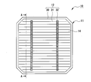
- FIG.1 and FIG.2 it demonstrates in full detail about the structure of the solar cell 10 which is 1st Embodiment.
- FIG. 1 is a plan view of the solar cell 10 as viewed from the light receiving surface side.
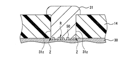
- FIG. 2 is a diagram showing a part of the AA line cross section of FIG. 1, and shows a cross section of the solar cell 10 cut in the thickness direction along a direction orthogonal to the finger portions 31.
- the solar cell 10 is formed on the photoelectric conversion unit 11 that generates carriers by receiving sunlight, the light receiving surface electrode 12 formed on the light receiving surface of the photoelectric conversion unit 11, and the back surface of the photoelectric conversion unit 11.
- the back electrode 13 is provided. In the solar cell 10, carriers generated by the photoelectric conversion unit 11 are collected by the light receiving surface electrode 12 and the back surface electrode 13.
- the “light-receiving surface” means a main surface on which sunlight mainly enters from the outside of the solar cell 10. For example, more than 50% to 100% of the sunlight incident on the solar cell 10 enters from the light receiving surface side.
- the “back surface” means a main surface opposite to the light receiving surface. Note that a surface along the thickness direction of the solar cell 10 and perpendicular to the main surface is a side surface.
- the photoelectric conversion unit 11 includes, for example, a semiconductor substrate 20, an amorphous semiconductor layer 21 formed on the light receiving surface side of the substrate 20, and an amorphous semiconductor layer 22 formed on the back surface side of the substrate 20.
- the amorphous semiconductor layers 21 and 22 respectively cover the entire light receiving surface and back surface of the substrate 20 (including a state that can be regarded as substantially the entire region, for example, a state in which 95% of the light receiving surface is covered. The same applies hereinafter). .
- the substrate 20 include an n-type single crystal silicon substrate.
- the amorphous semiconductor layer 21 has a layer structure in which, for example, an i-type amorphous silicon layer and a p-type amorphous silicon layer are sequentially formed.
- the amorphous semiconductor layer 22 has a layer structure in which, for example, an i-type amorphous silicon layer and an n-type amorphous silicon layer are sequentially formed.
- the photoelectric conversion unit 11 has an i-type amorphous silicon layer and an n-type amorphous silicon layer sequentially formed on the light-receiving surface of the n-type single crystal silicon substrate.
- a structure in which an i-type amorphous silicon layer and a p-type amorphous silicon layer are formed in order may be employed.
- the light receiving surface and the back surface of the substrate 20 have a texture structure (not shown).
- the texture structure is a surface uneven structure that suppresses surface reflection and increases the light absorption amount of the photoelectric conversion unit 11.
- the uneven height of the texture structure is about 1 ⁇ m to 15 ⁇ m. Since the thicknesses of the amorphous semiconductor layers 21 and 22 and the transparent conductive layers 30 and 40 described later are about several nanometers to several hundreds of nanometers, irregularities of the texture structure also appear on the transparent conductive layers 30 and 40.
- the light receiving surface electrode 12 includes a transparent conductive layer 30 formed on the light receiving surface of the photoelectric conversion unit 11.
- the transparent conductive layer 30 (the same applies to the transparent conductive layer 40) is obtained by doping metal oxide such as indium oxide (In 2 O 3 ) or zinc oxide (ZnO) with tin (Sn), antimony (Sb), or the like. It is comprised from a transparent conductive oxide (henceforth "TCO").
- the transparent conductive layer 30 (the same applies to the transparent conductive layer 40) may cover the entire area on the amorphous semiconductor layer 21, but in the form shown in FIG. The whole area except for is covered.
- the thickness of the transparent conductive layers 30 and 40 is preferably about 30 nm to 500 nm, and particularly preferably about 50 nm to 200 nm.
- the light-receiving surface electrode 12 includes a plurality of (for example, 50) finger portions 31 formed on the transparent conductive layer 30 as a collecting electrode for collecting carriers through the transparent conductive layer 30.
- the present embodiment further includes a plurality of (for example, two) bus bar portions 32 that are formed on the transparent conductive layer 30 so as to extend in a direction intersecting the finger portions 31.
- the finger part 31 is a thin wire electrode formed over a wide area on the transparent conductive layer 30.
- the bus bar part 32 is an electrode that collects carriers from the finger part 31, and is an electrode to which a wiring material is connected when the solar cell 10 is modularized, for example.
- the finger part 31 and the bus bar part 32 are plating electrodes formed by an electrolytic plating method.
- the finger part 31 and the bus bar part 32 may be collectively referred to as “collecting electrode” or “plating electrode”.
- the plating electrode is formed on the transparent conductive layer 30 where the coating layer 14 is not formed.
- the plating electrode is made of, for example, a metal such as nickel (Ni), copper (Cu), silver (Ag), etc., and a laminated structure of a nickel plating layer and a copper plating layer is suitable.
- An insulating coating layer 14 is formed on the transparent conductive layer 30.
- the coating layer 14 is preferably formed over the entire light receiving surface except for the region where the plating electrode is formed. In this embodiment, the coating layer 14 is also formed on the edge of the amorphous semiconductor layer 21. Yes.
- the thickness of the coating layer 14 is 20 ⁇ m to 30 ⁇ m, for example, and is slightly thinner than the thickness of the plating electrode.
- the material constituting the coating layer 14 is preferably a photocurable resin containing an epoxy resin or the like from the viewpoints of productivity, insulation, adhesion to the module filler, and the like.
- the back electrode 13 includes a transparent conductive layer 40 formed on the amorphous semiconductor layer 22, a metal layer 41 formed over the entire area of the transparent conductive layer 40, and a plurality of bus bar portions formed on the metal layer 41. 42 is preferable.
- the metal layer 41 is a thin film made of a metal material such as silver (Ag) having high light reflectivity and high conductivity.
- the thickness of the metal layer 41 is, for example, about 0.1 ⁇ m to 5 ⁇ m.
- the back surface electrode 13 may change the metal layer 41 into a finger part, and may form the said finger part and the bus-bar part 42 by electrolytic plating.
- the configuration of the transparent conductive layer 30 will be further described in detail with reference to FIGS. 3 and 4.
- FIG. 3 is an enlarged view showing a section in the vicinity of the surface of the transparent conductive layer 30 (an enlarged view of a portion B in FIG. 2)
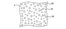
- FIG. 4 is a plan view showing a bonding surface R of the transparent conductive layer 30.
- the transparent conductive layer 30 has a plurality of particles 50 on its surface (see FIG. 3).
- the particles 50 are preferably selectively present on the bonding surface R, which is a bonding portion with the collector electrode, of the surface of the transparent conductive layer 30.
- the particles 50 protrude from the surface of the transparent conductive layer 30.
- the particles 50 have a curved shape such as a dome shape, a hemispherical shape, a spherical shape, or a spindle shape, and there are particularly many hemispherical or spherical shapes.
- the particles 50 can be formed by reducing TCO constituting the transparent conductive layer 30. That is, in this embodiment, the particle 50 is composed of a part of the transparent conductive layer 30 and can be said to be a granular protrusion.
- the composition of the particles 50 is a reduced product of TCO.
- TCO is a metal oxide containing indium oxide (In 2 O 3 ) as a main component
- the composition of the particles 50 is In rich compared to In 2 O 3 constituting the portion other than the bonding surface R. Indium oxide or In.
- the particle diameter D of the particles 50 is preferably 10 nm to 200 nm, and at least the average particle diameter of the particles 50 is preferably 10 nm to 200 nm.
- the particle diameter D is measured using a scanning electron microscope (SEM) or a transmission electron microscope (TEM).
- SEM scanning electron microscope
- TEM transmission electron microscope
- the major axis is the particle size D.
- the major axis of the particle 50 is defined as the long side of the circumscribed rectangle of the particle 50 defined in the two-dimensional microscope image (the short side of the circumscribed rectangle is defined as the minor axis of the particle 50).
- the average particle diameter is an average value of the particle diameter D and corresponds to a so-called number average diameter.
- the average particle diameter is an average value of the particle diameters D of all the particles 50 existing in the range of 10 ⁇ m ⁇ 10 ⁇ m on the bonding surface R.
- the particles 50 are present uniformly over the entire bonding surface R (see FIG. 4).
- the bonding surface R does not include a portion where the number of the particles 50 is extremely large or small, and the particles 50 are present uniformly at random.
- the density K of the particles 50 is the same (substantially equivalent) over the entire bonding surface R, for example, a two-dimensional microscopic image of the bonding surface R is divided into a plurality of sections having the same area. In some cases, the difference in the density K of each section includes a state within 5%.
- the density K is preferably 10% to 100%, more preferably 20% to 80%, and particularly preferably 25% to 75%. Further, from the relationship between the density K and the number average particle diameter Dn, it is possible to sufficiently improve the adhesion between the transparent conductive layer 30 and the collector electrode while suppressing a significant increase in sheet resistance.
- the thickness of the portion corresponding to the bonding surface R where the particles 50 are present is thinner than the thickness of the other portions.
- the transparent conductive layer 30 has a thinned portion where the TCO reduction treatment has been performed.
- the sheet resistance of the bonding surface R is higher than the sheet resistance of other portions.
- the sheet resistance of the bonding surface R is, for example, about 1.05 to 5 times higher than the sheet resistance of other portions.
- the sheet resistance of the bonding surface R tends to increase as the density K increases or as the number average particle diameter Dn increases.
- the sheet resistance can be measured by a known method (for example, a four probe method).
- the sheet resistance directly under the collector electrode, that is, the bonding surface R may be high. This is because the carriers flowing through the collector electrode can be collected from a region Z (also referred to as a boundary region between the bonding surface R and the other portion) of the transparent conductive layer 30 directly below the side surface 31z of the collector electrode.
- Particles may be provided on the surface of the transparent conductive layer 40. Since the metal layer 41 is formed over the entire area of the transparent conductive layer 40, for example, particles are provided over the entire surface of the transparent conductive layer 40 to improve the adhesion between the transparent conductive layer 40 and the metal layer 41. Can do.
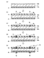
- FIG. 5 is a diagram illustrating an example of a manufacturing process of the solar cell 10.
- the portion where the particles 50 are formed is indicated by mesh hatching.
- the collector electrode is formed by two electrolytic plating processes including a nickel plating process and a copper plating process using the coating layer 14 as a mask, and the bus bar portion 42 is formed by a screen printing method using a conductive paste. .
- the photoelectric conversion unit 11 is manufactured by a known method (a detailed description of the manufacturing process of the photoelectric conversion unit 11 is omitted).
- the photoelectric conversion unit 11 is prepared, the light receiving surface electrode 12 is formed on the light receiving surface of the photoelectric conversion unit 11, and the back electrode 13 is formed on the back surface of the photoelectric conversion unit 11.
- transparent conductive layers 30 a and 40 a that are precursors of the transparent conductive layers 30 and 40 are formed on the light receiving surface and the back surface of the photoelectric conversion unit 11, respectively, and then on the transparent conductive layer 40 a.
- a metal layer 41 is formed on the substrate (FIG. 5A).
- the transparent conductive layers 30a and 40a and the metal layer 41 can be formed using, for example, a sputtering method.
- FIGS. 5B to 5D show a mask forming process, a particle forming process, and an electrolytic plating process, respectively.
- the coating layer 14 made of a photocurable resin is formed as a mask on the transparent conductive layer 30a.
- the patterned coating layer 14 is formed over the entire area on the light receiving surface.
- the patterned coating layer 14 can be formed by a known method. For example, after a thin film layer made of a photocurable resin is formed on the light receiving surface by spin coating, spraying, or the like, the coating layer 14 patterned by a photolithography process is formed. Further, the patterned coating layer 14 may be formed by using a printing method such as screen printing.
- the coating layer 14 is patterned so as to expose a surface Ra (a surface Ra serving as the bonding surface R), which is a portion for forming a collector electrode, of the surface of the transparent conductive layer 30a. That is, an opening 33 corresponding to the bonding surface R is formed in the coating layer 14.
- the coating layer 14 also functions as a mask in the particle forming process.
- a particle forming process is provided between the mask forming process and the electrolytic plating process.
- the particle forming step is a step of forming the particles 50 by reducing TCO on the surface Ra exposed from the openings 33.
- TCO is reduced, the amount of oxygen in TCO decreases and sheet resistance decreases at the initial stage of reduction, but in this step, the reduction is further advanced. Thereby, sheet resistance becomes higher than before reduction
- TCO is indium oxide (In 2 O 3 )
- the method for the reduction treatment is not particularly limited as long as the method can selectively reduce TCO on the surface Ra to precipitate the particles 50.
- reduction by hydrogen plasma treatment or electrolytic reduction can be mentioned.
- the former is a gas phase reduction method and the latter is a liquid phase reduction method.
- electrolytic reduction for example, an aqueous ammonium sulfate solution is used as the electrolyte solution, and the photoelectric conversion unit 11 on which the coating layer 14 is formed is used as a cathode and the platinum plate is used as an anode. And the photoelectric conversion part 11 and a platinum plate are immersed in an electrolyte solution, and an electric current is applied between both.
- the negative pole of the power supply device is connected to the photoelectric conversion unit 11 at a part on the surface Ra exposed from the opening 33.
- the particle size D and density K of the particles 50 can be adjusted by, for example, the amount of current applied (current ⁇ time). As the amount of current increases, the particle diameter D usually increases and the density K increases.
- electrolytic plating is performed using the photoelectric conversion portion 11 on which the coating layer 14 is formed as a cathode and the nickel plate as an anode.
- the negative pole of the power supply device is connected to the photoelectric conversion unit 11 at a part on the surface Rb exposed from the opening 33.
- Electrolytic plating is in a state where an insulating coating is formed on the back surface so as not to deposit a metal plating layer on the back surface of the photoelectric conversion unit 11 (for example, an insulating resin layer covering the back surface is formed and removed after the electrolytic plating step).
- the photoelectric conversion unit 11 and the nickel plate are immersed in a plating solution, and a current is applied between them.
- the plating solution a known nickel plating solution containing nickel sulfate or nickel chloride can be used. In this way, a nickel plating layer is formed on the surface Rb exposed from the opening 33 and on which a large number of particles 50 are formed.
- electrolytic plating is performed using a copper plate as an anode and a known copper plating solution containing copper sulfate or copper cyanide.
- a copper plating layer is formed on the nickel plating layer formed previously, and the finger part 31 and the bus-bar part 32 comprised from a nickel plating layer and a copper plating layer are formed.
- the thickness of the metal plating layer is, for example, about 30 ⁇ m to 50 ⁇ m, and can be adjusted by the amount of current applied (current ⁇ time).
- a bus bar portion 42 is formed on the metal layer 41 by screen printing (FIG. 5E).
- conductive printing for example, silver paste
- the solvent contained in the paste is volatilized to form the bus bar portion 42.
- the conductive paste include a thermosetting binder resin such as an epoxy resin, a conductive filler such as silver or carbon dispersed in the binder resin, and a solvent such as butyl carbitol acetate (BCA). That is, the bus bar portion 42 is made of a binder resin in which a conductive filler is dispersed.
- this heat treatment step is a step for removing the solvent of the conductive paste to thermally cure the binder resin, and an annealing step for crystallizing TCO.
- a large number of particles 50 can be provided on the surface R of the transparent conductive layer 30 on the bonding surface R with the collector electrode. That is, irregularities of the order of several tens to several hundreds of nanometers are formed on the bonding surface R, and the surface area of the bonding surface R is greatly increased. For this reason, the contact area between the transparent conductive layer 30 and the collector electrode is greatly increased, and the adhesion between them can be improved.
- the particles 50 are selectively provided only on the bonding surface R due to the presence of the coating layer 14, it is possible to prevent light reception loss due to the particles 50.
- the solar cell 10 forms a collector electrode by an electrolytic plating method, it can be manufactured at a lower cost than other methods (for example, a sputtering method or a screen printing method).
- the plating electrode is generally inferior in adhesion to the transparent conductive layer as compared with electrodes formed by other methods, according to the solar cell 10, the adhesion between the plating electrode and the transparent conductive layer 30 is improved. Thus, peeling of the plating electrode can be sufficiently suppressed.
- the particles 50 exist with a uniform density K over the entire bonding surface R, the adhesion between the plating electrode and the transparent conductive layer 30 can be dramatically improved. As described above, this form can be formed by reducing the amorphous TCO to precipitate the particles 50 and then crystallizing the TCO.
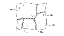
- FIG. 6 is a plan view showing the bonding surface Rx of the transparent conductive layer 30x
- FIG. 7 is a diagram showing an example of the manufacturing process of the solar cell 10x.
- the portion where the particles 50x are formed is indicated by mesh hatching.
- the solar cell 10x has the same configuration as the solar cell 10 except for the transparent conductive layer 30x.
- the difference (transparent conductive layer 30x) from the solar cell 10 will be described in detail, and the same components as those of the solar cell 10 are denoted by the same reference numerals, and redundant description will be omitted.
- the manufacturing process of the solar cell 10x differs from the case of the solar cell 10, the processing method in each process is the same as that of the solar cell 10.
- particles 50x are present at a higher density in the portion where the TCO crystal grain boundary 51 constituting the transparent conductive layer 30x is formed in the bonding surface Rx (see FIG. 6).
- the crystal grain boundary 51 is formed in a mesh shape over the entire transparent conductive layer 30x.
- most of the particles 50 x exist in a line along the crystal grain boundary 51, and a small number of particles 50 x exist in a part away from the crystal grain boundary 51.
- the particles 50 x existing along the crystal grain boundary 51 tend to have a larger particle diameter Dx than the particles 50 x existing away from the crystal grain boundary 51.
- the solar cell 10x having the above-described configuration can be manufactured by annealing TCO and then reducing the crystallized TCO to precipitate particles 50x (see FIG. 7).
- the TCO is crystallized by a heat treatment process in the process of forming the bus bar portion 42 (FIG. 7B).
- the coating layer 14 is formed on the crystallized TCO as a mask, and the surface Rxa that becomes the bonding surface Rx is selectively reduced until the particles 50x are deposited (FIG. 7C). d)).
- the crystallized TCO is subjected to reduction treatment, particles 50x are selectively deposited at the crystal grain boundaries 51. In other words, it is difficult for TCO to be reduced at portions other than the crystal grain boundaries 51.
- the transparent conductive layer 30x in which the particles 50x are collected at the crystal grain boundary 51 is obtained.
- the surface area of the bonding surface Rx is increased by the particles 50x, and the adhesion between the transparent conductive layer 30x and the collector electrode can be improved.
- the solar cell 60 according to the second embodiment will be described in detail with reference to FIGS.
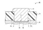
- FIG. 8 is a view showing a cross section of the transparent conductive layer 61 and the vicinity thereof
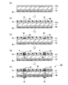
- FIG. 9 is a view showing an example of the manufacturing process of the solar cell 60.
- the solar cell 60 has the same configuration as the solar cell 10 except for the transparent conductive layer 61.
- the transparent conductive layer 61 will be described in detail, and the same components as those of the solar cell 10 will be denoted by the same reference numerals and redundant description will be omitted (in FIGS. 1 and 2, the reference numeral “30” is changed to “61”). If it changes, it will become the figure which shows the solar cell 60).
- the light-receiving surface electrode 12 includes a transparent conductive columnar crystal layer 62 formed on the light-receiving surface of the photoelectric conversion unit 11 and a transparent conductive non-columnar crystal layer formed on the columnar crystal layer 62. 63, and a finger part 31 and a bus bar part 32 which are collector electrodes formed on the non-columnar crystal layer 63.
- the columnar crystal layer 62 and the non-columnar crystal layer 63 are collectively referred to as a transparent conductive layer 61.
- the back electrode 13 includes the transparent conductive layer 40, but instead of this, a columnar crystal layer and a non-columnar crystal layer similar to those of the light receiving surface electrode 12 may be provided.
- the columnar crystal layer 62 is a layer in which crystal grain boundaries oriented in the same direction by cross-sectional observation using an SEM can be confirmed in almost the entire area of the observation cross-section.
- the “substantially entire area” includes a range that can be regarded as substantially the entire area, and means, for example, 95% or more of the observation cross section.
- contrast contrast is repeated in one direction, and a plurality of columns appear to be arranged in one direction. Or it looks striped. Such a contrasting light and dark boundary indicates a grain boundary.
- the non-columnar crystal layer 63 is a layer having a higher proportion of crystal grain boundaries oriented in different directions than crystal grain boundaries oriented in the same direction by cross-sectional observation using SEM.
- the portion where the contrast is repeated in one direction is less than 50%, and in some cases, the portion where the contrast is repeated regularly cannot be confirmed.
- the columnar crystal layer 62 is a layer in which all crystal grain boundaries are in the same orientation, and is on the photoelectric conversion unit 11 side when the photoelectric conversion unit 11 and the light receiving surface electrode 12 are compared.
- the non-columnar crystal layer 63 is a layer in which at least one crystal grain boundary is in the same orientation and all crystal grain boundaries are not in the same orientation, and the photoelectric conversion unit 11 and the light receiving surface electrode 12 are compared. At the light receiving surface electrode 12 side.
- the columnar crystal layer 62 is provided in a wider range than the non-columnar crystal layer 63.
- the non-columnar crystal layer 63 is selectively provided on the surface of the transparent conductive layer 61 on the bonding surface R, which is a bonding portion with the collector electrode, and a region immediately below the bonding surface R (hereinafter sometimes referred to as “bonding surface region”). It is preferred that And it is suitable not to provide the non-columnar crystal layer 63 in the part which receives sunlight other than a joining surface area
- the transparent conductive layer 61 in the bonding surface region has a stacked structure of the columnar crystal layer 62 and the non-columnar crystal layer 63, and the other part of the transparent conductive layer 61 is a single layer composed only of the columnar crystal layer 62. It has a layer structure.
- the composition of the columnar crystal layer 62 is crystallized TCO
- the composition of the non-columnar crystal layer 63 is a reduced product of TCO.
- TCO is a metal oxide containing indium oxide (In 2 O 3 ) as a main component
- the composition of the non-columnar crystal layer 63 is in comparison with In 2 O 3 constituting a portion other than the junction surface region. In-rich indium oxide or In.
- the thickness of the transparent conductive layer 61 is preferably about 30 nm to 500 nm, and particularly preferably about 50 nm to 200 nm.
- the non-columnar crystal layer 63 is preferably thinner than the columnar crystal layer 62.
- the ratio of the thickness of the non-columnar crystal layer 63 to the thickness of the columnar crystal layer 62 is preferably about 0.2 to 0.8, A range of about 0.3 to 0.6 is particularly preferable.
- the thickness of the columnar crystal layer 62 is 80 nm
- the thickness of the non-columnar crystal layer 63 is 20 nm.
- this thickness is an average value of the length along the thickness direction measured by cross-sectional observation using SEM.
- the thickness of the portion where the non-columnar crystal layer 63 is formed is thinner than the thickness of other portions.
- the transparent conductive layer 61 has a thinned portion where the TCO reduction process has been performed.
- the non-columnar crystal layer 63 may exist over substantially the entire bonding surface R, or may exist in a part thereof.
- the area of the non-columnar crystal layer 63 is equal to the bonding surface. It is preferably 20% to 80% of the area of R, particularly preferably 25% to 75%.
- the non-columnar crystal layer 63 exists uniformly on the bonding surface R.
- the sheet resistance of the non-columnar crystal layer 63 is higher than the sheet resistance of the columnar crystal layer 62.
- the sheet resistance of the non-columnar crystal layer 63 is, for example, about 1.05 to 5 times higher than the sheet resistance of the columnar crystal layer 62.
- the sheet resistance can be measured by a known method (for example, a four probe method).
- the sheet resistance of the bonding surface region may be high. This is because the carriers flowing through the collector electrode can be collected from the region Z immediately below the side surface 31z of the collector electrode in the transparent conductive layer 61.
- FIG. 9 is a diagram illustrating an example of a manufacturing process of the solar cell 60.
- the collector electrode is formed by two electrolytic plating processes including a nickel plating process and a copper plating process using the coating layer 14 as a mask, and the bus bar portion 42 is formed by a screen printing method using a conductive paste. .
- the columnar crystal layer 62 is formed when the TCO layer is formed.
- the method for forming the columnar crystal layer 62 and the non-columnar crystal layer 63 is not limited to this.
- the columnar crystal layer 62 may be formed by heat-treating the TCO layer having the non-columnar crystal layer 63 after the non-columnar crystal layer 63 is formed.
- the photoelectric conversion unit 11 is manufactured by a known method (a detailed description of the manufacturing process of the photoelectric conversion unit 11 is omitted).
- the photoelectric conversion unit 11 is prepared, the light receiving surface electrode 12 is formed on the light receiving surface of the photoelectric conversion unit 11, and the back electrode 13 is formed on the back surface of the photoelectric conversion unit 11.
- the transparent conductive layer 61 a that is a precursor of the transparent conductive layer 61 is formed on the light receiving surface of the photoelectric conversion unit 11, and the transparent conductive layer 40 is formed on the back surface of the photoelectric conversion unit 11.
- a metal layer 41 is formed on the transparent conductive layer 40 (FIG. 9A).
- the transparent conductive layers 61a and 40 can be formed using, for example, chemical vapor deposition (CVD). Film formation by the CVD method is preferably performed under a temperature condition of about 200 ° C. to 300 ° C. TCO is crystallized by such heat to form the columnar crystal layer 62.
- the metal layer 41 can be formed using, for example, a sputtering method.
- FIGS. 9B to 9D show a mask forming process, a non-columnar crystal layer forming process, and an electrolytic plating process, respectively.
- the coating layer 14 made of a photocurable resin is formed as a mask on the transparent conductive layer 61a.
- the patterned coating layer 14 is formed over the entire area on the light receiving surface.
- the patterned coating layer 14 can be formed by a known method. For example, after a thin film layer made of a photocurable resin is formed on the light receiving surface by spin coating, spraying, or the like, the coating layer 14 patterned by a photolithography process is formed. Further, the patterned coating layer 14 may be formed by using a printing method such as screen printing.
- the coating layer 14 is patterned so as to expose the surface Ra (surface Ra serving as the bonding surface R), which is a portion for forming the collector electrode, of the surface of the transparent conductive layer 61a. That is, an opening 33 corresponding to the bonding surface R is formed in the coating layer 14.
- the coating layer 14 also functions as a mask in the non-columnar crystal layer forming step.
- a non-columnar crystal layer forming step is provided between the mask forming step and the electrolytic plating step.
- the non-columnar crystal layer forming step is a step of forming the non-columnar crystal layer 63 by reducing TCO on the surface Ra of the transparent conductive layer 61 a composed of the columnar crystal layer 62 exposed from the opening 33.
- TCO When TCO is reduced, the amount of oxygen in TCO decreases and sheet resistance decreases at the initial stage of reduction, but in this step, the reduction is further advanced. As a result, the sheet resistance becomes higher than before reduction, and the non-columnar crystal layer 63 is formed in the surface Ra and the region immediately below the surface Ra.
- the non-columnar crystal layer 63 having a high indium (In) ratio is formed.
- the transparent conductive layer 61 having the columnar crystal layer 62 and the non-columnar crystal layer 63 is formed.
- the method of the reduction treatment is not particularly limited as long as the TCO on the surface Ra can be selectively reduced to form the non-columnar crystal layer 63.
- reduction by hydrogen plasma treatment or electrolytic reduction can be mentioned.
- the former is a gas phase reduction method and the latter is a liquid phase reduction method.
- electrolytic reduction for example, an aqueous ammonium sulfate solution is used as the electrolyte solution, and the photoelectric conversion unit 11 on which the coating layer 14 is formed is used as a cathode and the platinum plate is used as an anode. And the photoelectric conversion part 11 and a platinum plate are immersed in an electrolyte solution, and an electric current is applied between both.
- the negative pole of the power supply device is connected to the photoelectric conversion unit 11 at a part on the surface Ra exposed from the opening 33.
- the thickness of the non-columnar crystal layer 63 and the area on the bonding surface R can be adjusted by, for example, the amount of current to be applied (current ⁇ time). As the amount of current increases, the thickness of the non-columnar crystal layer 63 and the area on the bonding surface R generally increase.
- electrolytic plating is performed using the photoelectric conversion portion 11 on which the coating layer 14 is formed as a cathode and the nickel plate as an anode.
- the negative pole of the power supply device is connected to the photoelectric conversion unit 11 on a part of the surface Rb of the transparent conductive layer 61 exposed from the opening 33.
- Electrolytic plating is in a state where an insulating coating is formed on the back surface so as not to deposit a metal plating layer on the back surface of the photoelectric conversion unit 11 (for example, an insulating resin layer covering the back surface is formed and removed after the electrolytic plating step).
- the photoelectric conversion unit 11 and the nickel plate are immersed in a plating solution, and a current is applied between them.
- the plating solution a known nickel plating solution containing nickel sulfate or nickel chloride can be used.
- a nickel plating layer is formed on the surface Rb exposed from the opening 33 and having the non-columnar crystal layer 63 formed thereon.
- electrolytic plating is performed using a copper plate as an anode and a known copper plating solution containing copper sulfate or copper cyanide.
- a copper plating layer is formed on the nickel plating layer formed previously, and the finger part 31 and the bus-bar part 32 comprised from a nickel plating layer and a copper plating layer are formed.
- the thickness of the metal plating layer is, for example, about 30 ⁇ m to 50 ⁇ m, and can be adjusted by the amount of current applied (current ⁇ time).
- a bus bar portion 42 is formed on the metal layer 41 by screen printing (FIG. 9E).
- conductive printing for example, silver paste
- the solvent contained in the paste is volatilized to form the bus bar portion 42.
- the conductive paste include a thermosetting binder resin such as an epoxy resin, a conductive filler such as silver or carbon dispersed in the binder resin, and a solvent such as butyl carbitol acetate (BCA). That is, the bus bar portion 42 is made of a binder resin in which a conductive filler is dispersed.
- heat treatment is performed under conditions of 200 ° C. ⁇ 60 minutes.
- the columnar crystal layer 62 can also be formed by a heat treatment when forming the bus bar portion 42. For example, after forming the TCO layer by sputtering (non-heating conditions) and forming the non-columnar crystal layer 63 as described above, in this heat treatment step, the portion other than the non-columnar crystal layer 63 is crystallized to crystallize the columnar crystal layer. 62 can be formed.
- the non-columnar crystal layer 63 is provided on the bonding surface R of the transparent conductive layer 61 and the region immediately below the bonding surface R, and a stacked structure of the columnar crystal layer 62 and the non-columnar crystal layer 63 can be obtained. Since the adhesive force between the non-columnar crystal layer 63 and the collector electrode is larger than the adhesive force between the columnar crystal layer 62 and the collector electrode, the transparent conductive layer according to the solar cell 60 having the non-columnar crystal layer 63 on the bonding surface R. The adhesion between 61 and the collector electrode can be improved.
- the non-columnar crystal layer 63 is less transparent than the columnar crystal layer 62, but is selectively provided only on the bonding surface R due to the presence of the coating layer 14. Can be prevented.
- the solar cell 60 forms a collector electrode by an electrolytic plating method, it can be manufactured at a lower cost than other methods (for example, a sputtering method or a screen printing method).
- the plating electrode is generally inferior in adhesion to the transparent conductive layer as compared with electrodes formed by other methods, the solar cell 60 improves the adhesion between the plating electrode and the transparent conductive layer 61. Thus, peeling of the plating electrode can be sufficiently suppressed.
- FIG.10 and FIG.11 it demonstrates in full detail about the solar cell 70 which is 3rd Embodiment.
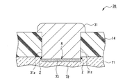
- FIG. 10 is a view showing a cross section of the transparent conductive layer 71 and the vicinity thereof
- FIG. 11 is a view showing an example of a manufacturing process of the solar cell 70.
- the solar cell 70 has the same configuration as the solar cell 10 except for the transparent conductive layer 71.
- the transparent conductive layer 71 will be described in detail, and the same components as those of the solar cell 10 will be denoted by the same reference numerals, and redundant description will be omitted (in FIG. 1 and FIG. If it changes, it will become the figure which shows the solar cell 70).
- the light receiving surface electrode 12 has a density higher than that of the transparent conductive high density layer 72 formed on the light receiving surface of the photoelectric conversion unit 11 and the high density layer 72 formed on the high density layer 72.
- the transparent conductive low density layer 73 having a low thickness, and the finger part 31 and the bus bar part 32 which are collector electrodes formed on the low density layer 73.
- the high density layer 72 and the low density layer 73 are collectively referred to as a transparent conductive layer 71.
- the back surface electrode 13 has the transparent conductive layer 40, it may replace with this and may provide the high density layer and low density layer similar to the light-receiving surface electrode 12.
- the high density layer 72 is a layer in which a darker and darker image than the low density layer 73 is obtained in a cross-sectional observation image using an SEM. That is, in the SEM image, the degree of scattering and absorption of the electron beam is different in proportion to the difference in density, and the portion having a high density becomes dark because the transmittance of the electron beam is small.
- the contrast density is repeated in one direction in almost the entire area of the observation cross section, and appears to be striped. Such a contrasting light and dark boundary indicates a grain boundary.
- the portion where the contrast density is repeated in one direction is less than 50%, and in some cases, the portion where the contrast density is regularly repeated cannot be confirmed.
- the high density layer 72 is provided in a wider range than the low density layer 73.
- the high-density layer 72 is selectively provided on the bonding surface R, which is a bonding portion with the collector electrode, of the surface of the transparent conductive layer 71 and a region immediately below the bonding surface R (hereinafter sometimes referred to as “bonding surface region”). Is preferred. And it is suitable not to provide the high-density layer 72 in the part which receives sunlight other than a joining surface area
- the transparent conductive layer 71 in the bonding surface region has a laminated structure of the high-density layer 72 and the low-density layer 73, and the other part of the transparent conductive layer 71 is a single layer composed only of the high-density layer 72. It has a structure.
- the composition of the high density layer 72 is crystallized TCO
- the composition of the low density layer 73 is a reduced product of TCO.
- the TCO is a metal oxide containing indium oxide (In 2 O 3 ) as a main component
- the composition of the low density layer 73 is In compared with In 2 O 3 constituting a portion other than the junction surface region. Rich indium oxide or In.
- the thickness of the transparent conductive layer 71 is preferably about 30 nm to 500 nm, and particularly preferably about 50 nm to 200 nm.
- the thickness of the low density layer 73 is preferably thinner than the thickness of the high density layer 72.
- the ratio of the thickness of the low density layer 73 to the thickness of the high density layer 72 is preferably about 0.2 to 0.8.
- a range of about 3 to 0.6 is particularly preferable.
- the thickness of the high density layer 72 is 80 nm, and the thickness of the low density layer 73 is 20 nm.
- this thickness is an average value of the length along the thickness direction measured by cross-sectional observation using SEM.
- the thickness of the portion where the low density layer 73 is formed is thinner than the thickness of the other portions.
- the transparent conductive layer 71 has a thinned portion where the TCO reduction process has been performed.
- the low density layer 73 may exist over substantially the entire bonding surface R, or may exist in a part thereof.
- the area of the low density layer 73 is the area of the bonding surface R. It is preferably 20% to 80%, particularly preferably 25% to 75%. Moreover, it is preferable that the low-density layer 73 exists uniformly on the bonding surface R.
- the sheet resistance of the low density layer 73 is higher than the sheet resistance of the high density layer 72.
- the sheet resistance of the low density layer 73 is, for example, about 1.05 to 5 times higher than the sheet resistance of the high density layer 72.
- the sheet resistance can be measured by a known method (for example, a four probe method).
- the sheet resistance of the bonding surface region may be high. This is because the carriers flowing through the collector electrode can be collected from the region Z immediately below the side surface 31z of the collector electrode in the transparent conductive layer 71.
- FIG. 11 is a diagram illustrating an example of a manufacturing process of the solar cell 70.
- the collector electrode is formed by two electrolytic plating processes including a nickel plating process and a copper plating process using the coating layer 14 as a mask, and the bus bar portion 42 is formed by a screen printing method using a conductive paste. .
- the high density layer 72 is formed when the TCO layer is formed.
- the formation method of the high density layer 72 and the low density layer 73 is not limited to this.
- the high density layer 72 may be formed by heat-treating the TCO layer having the high density layer 72 after the low density layer 73 is formed.
- the photoelectric conversion unit 11 is manufactured by a known method (a detailed description of the manufacturing process of the photoelectric conversion unit 11 is omitted).
- the photoelectric conversion unit 11 is prepared, the light receiving surface electrode 12 is formed on the light receiving surface of the photoelectric conversion unit 11, and the back electrode 13 is formed on the back surface of the photoelectric conversion unit 11.
- the transparent conductive layer 71 a that is a precursor of the transparent conductive layer 71 is formed on the light receiving surface of the photoelectric conversion unit 11, and the transparent conductive layer 40 is formed on the back surface of the photoelectric conversion unit 11.
- a metal layer 41 is formed on the transparent conductive layer 40 (FIG. 11A).
- the transparent conductive layers 71a and 40 can be formed using, for example, chemical vapor deposition (CVD). Film formation by the CVD method is preferably performed under a temperature condition of about 200 ° C. to 300 ° C. The TCO is crystallized by such heat to form the high-density layer 72.
- the metal layer 41 can be formed using, for example, a sputtering method.
- FIGS. 11B to 11D show a mask forming process, a low density layer forming process, and an electrolytic plating process, respectively.
- the coating layer 14 made of a photocurable resin is formed as a mask on the transparent conductive layer 71a.
- the patterned coating layer 14 is formed over the entire area on the light receiving surface.
- the patterned coating layer 14 can be formed by a known method. For example, after a thin film layer made of a photocurable resin is formed on the light receiving surface by spin coating, spraying, or the like, the coating layer 14 patterned by a photolithography process is formed. Further, the patterned coating layer 14 may be formed by using a printing method such as screen printing.
- the coating layer 14 is patterned so as to expose the surface Ra (surface Ra serving as the bonding surface R), which is a portion of the surface of the transparent conductive layer 71a where the collector electrode is formed. That is, an opening 33 corresponding to the bonding surface R is formed in the coating layer 14.
- the coating layer 14 also functions as a mask in the low density layer forming process.
- a low density layer forming step is provided between the mask forming step and the electrolytic plating step.
- the low density layer forming step is a step of forming the low density layer 73 by reducing TCO on the surface Ra of the transparent conductive layer 71 a composed of the high density layer 72 exposed from the opening 33.
- TCO is reduced, the amount of oxygen in TCO decreases and sheet resistance decreases at the initial stage of reduction, but in this step, the reduction is further advanced.
- the sheet resistance is higher than before reduction, and the low density layer 73 is formed on the surface Ra and the region immediately below the surface Ra.
- the TCO is indium oxide (In 2 O 3 )
- the low density layer 73 with a high indium (In) ratio is formed.
- the transparent conductive layer 71 having the high density layer 72 and the low density layer 73 is formed.
- the method of the reduction treatment is not particularly limited as long as the method can selectively reduce TCO on the surface Ra to form the low density layer 73.
- reduction by hydrogen plasma treatment or electrolytic reduction can be mentioned.
- the former is a gas phase reduction method and the latter is a liquid phase reduction method.
- electrolytic reduction for example, an aqueous ammonium sulfate solution is used as the electrolyte solution, and the photoelectric conversion unit 11 on which the coating layer 14 is formed is used as a cathode and the platinum plate is used as an anode. And the photoelectric conversion part 11 and a platinum plate are immersed in an electrolyte solution, and an electric current is applied between both.
- the negative pole of the power supply device is connected to the photoelectric conversion unit 11 at a part on the surface Ra exposed from the opening 33.
- the thickness of the low-density layer 73 and the area on the bonding surface R can be adjusted by, for example, the amount of current to be applied (current ⁇ time). As the amount of current increases, the thickness of the low-density layer 73 and the area on the bonding surface R usually increase.
- electrolytic plating is performed using the photoelectric conversion portion 11 on which the coating layer 14 is formed as a cathode and the nickel plate as an anode.
- the negative pole of the power supply device is connected to the photoelectric conversion unit 11 at a part on the surface Rb of the transparent conductive layer 71 exposed from the opening 33.
- Electrolytic plating is in a state where an insulating coating is formed on the back surface so as not to deposit a metal plating layer on the back surface of the photoelectric conversion unit 11 (for example, an insulating resin layer covering the back surface is formed and removed after the electrolytic plating step).
- the photoelectric conversion unit 11 and the nickel plate are immersed in a plating solution, and a current is applied between them.
- the plating solution a known nickel plating solution containing nickel sulfate or nickel chloride can be used.
- a nickel plating layer is formed on the surface Rb exposed from the opening 33 and on which the low density layer 73 is formed.
- electrolytic plating is performed using a copper plate as an anode and a known copper plating solution containing copper sulfate or copper cyanide.
- a copper plating layer is formed on the nickel plating layer formed previously, and the finger part 31 and the bus-bar part 32 comprised from a nickel plating layer and a copper plating layer are formed.
- the thickness of the metal plating layer is, for example, about 30 ⁇ m to 50 ⁇ m, and can be adjusted by the amount of current applied (current ⁇ time).
- a bus bar portion 42 is formed on the metal layer 41 by screen printing (FIG. 9E).
- conductive printing for example, silver paste
- the solvent contained in the paste is volatilized to form the bus bar portion 42.
- the conductive paste include a thermosetting binder resin such as an epoxy resin, a conductive filler such as silver or carbon dispersed in the binder resin, and a solvent such as butyl carbitol acetate (BCA). That is, the bus bar portion 42 is made of a binder resin in which a conductive filler is dispersed.
- heat treatment is performed under conditions of 200 ° C. ⁇ 60 minutes.
- the high-density layer 72 can also be formed by heat treatment when the bus bar portion 42 is formed. For example, after forming the TCO layer by sputtering (non-heating conditions) and forming the low-density layer 73 as described above, the high-density layer 72 is formed by crystallizing portions other than the low-density layer 73 in this heat treatment step. Can be formed.
- the laminated structure of the high-density layer 72 and the low-density layer 73 can be obtained by providing the low-density layer 73 on the bonding surface R of the transparent conductive layer 71 and the region immediately below the bonding surface R. Since the adhesion between the low density layer 73 and the collector electrode is greater than the adhesion between the high density layer 72 and the collector electrode, according to the solar cell 70 having the low density layer 73 on the bonding surface R, the transparent conductive layer 71 and The adhesion with the collector electrode can be improved.
- the low-density layer 73 is less transparent than the high-density layer 72, but is selectively provided only on the bonding surface R due to the presence of the coating layer 14. Can be prevented.
- the solar cell 70 forms a collector electrode by an electrolytic plating method, it can be manufactured at a lower cost than other methods (for example, a sputtering method or a screen printing method).
- the plating electrode is generally inferior in adhesion to the transparent conductive layer as compared with electrodes formed by other methods, the solar cell 70 improves the adhesion between the plating electrode and the transparent conductive layer 71. Thus, peeling of the plating electrode can be sufficiently suppressed.
- the particles 50 and 50x are precipitated by TCO reduction treatment
- particles may be added on the transparent conductive layer.
- conductive nanoparticles such as silver and nickel as the particles.
- a dispersion in which nanoparticles are dispersed can be applied on the transparent conductive layer to obtain a structure in which the nanoparticles are adhered on the transparent conductive layer.
- the finger part 31 and the bus bar part 32 are described as plating electrodes formed by an electrolytic plating method.
- electrodes formed by a sputtering method or a screen printing method may be used.
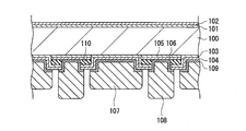
- the photoelectric conversion unit 11 can be appropriately changed in addition to the structure described above.
- an i-type amorphous silicon layer 101 and an n-type amorphous silicon film 102 are formed on the surface side of the n-type single crystal silicon substrate 100.
- a p-type region composed of an i-type amorphous silicon layer 103 and a p-type amorphous silicon layer 104, an i-type amorphous silicon layer 105, and an n-type amorphous silicon layer 106 It may be configured from the configured n-type region.
- an electrode is provided only on the back side of n-type single crystal silicon substrate 100.
- the electrode includes a p-side collector electrode 107 formed on the p-type region and an n-side collector electrode 108 formed on the n-type region.
- a transparent conductive layer 109 is formed between the p-type region and the p-side collector electrode 107 and between the n-type region and the n-side collector electrode 108.
- An insulating layer 110 is provided between the p-type region and the n-type region.
- a p-type polycrystalline silicon substrate 120 As shown in FIG. 13, a p-type polycrystalline silicon substrate 120, an n-type diffusion layer 121 formed on the front surface side of the p-type polycrystalline silicon substrate 120, and a back surface of the p-type polycrystalline silicon substrate 120. And an aluminum metal film 122 formed on the substrate.
Landscapes
- Photovoltaic Devices (AREA)
- Life Sciences & Earth Sciences (AREA)
- Engineering & Computer Science (AREA)
- Sustainable Development (AREA)
- Sustainable Energy (AREA)
Abstract
Description
Claims (19)
- 光電変換部と、
前記光電変換部の主面上に形成された透明導電層と、
前記透明導電層上に形成された集電極と、
を備え、
前記透明導電層は、その表面に粒子を有する太陽電池。 - 前記透明導電層は、透明導電性酸化物から構成され、
前記粒子の組成は、前記透明導電性酸化物の還元物である請求項1記載の太陽電池。 - 前記粒子の粒径は、10nm以上200nm以下である請求項1又は2記載の太陽電池。
- 前記粒子は、前記透明導電層の前記表面のうち前記集電極との接合部分に選択的に存在する請求項1~3のいずれか1項に記載の太陽電池。
- 前記粒子は、前記接合部分の全体に亘って一様に存在する請求項4記載の太陽電池。
- 前記粒子は、前記透明導電層の前記表面のうち前記透明導電性酸化物の結晶粒界が形成される部分において、その他の部分よりも高密度で存在する請求項1~5のいずれか1項に記載の太陽電池。
- 光電変換部と、
前記光電変換部の主面上に形成された電極と、
を備え、
前記電極は、
前記光電変換部の主面上に形成された透明導電性の柱状結晶層と、
前記柱状結晶層上に形成された透明導電性の非柱状結晶層と、
前記非柱状結晶層上に形成された集電極と、
を有する太陽電池。 - 前記柱状結晶層及び前記非柱状結晶層は、透明導電性酸化物から構成され、
前記非柱状結晶層の組成は、前記透明導電性酸化物の還元物である請求項7記載の太陽電池。 - 前記非柱状結晶層は、前記集電極との接合部分に選択的に存在する請求項7又は8記載の太陽電池。
- 光電変換部と、
前記光電変換部の主面上に形成された電極と、
を備え、
前記電極は、
前記光電変換部の主面上に形成された透明導電性の高密度層と、
前記高密度層上に形成され、前記高密度層よりも密度が低い透明導電性の低密度層と、
前記低密度層上に形成された集電極と、
を有する太陽電池。 - 前記高密度層及び前記低密度層は、透明導電性酸化物から構成され、
前記低密度層の組成は、前記透明導電性酸化物の還元物である請求項10記載の太陽電池。 - 前記低密度層は、前記集電極との接合部分に選択的に存在する請求項10又は11記載の太陽電池。
- 前記集電極は、金属めっき電極である請求項1~12のいずれか1項に記載の太陽電池。
- 光電変換部の主面上に透明導電性酸化物から構成される透明導電層を形成し、前記透明導電層の表面のうち集電極を形成する部分における前記透明導電性酸化物を還元して粒子を形成した後、当該部分上に前記集電極を形成する太陽電池の製造方法。
- 前記粒子の形成後に、前記透明導電性酸化物を熱処理して結晶化させる請求項14記載の太陽電池の製造方法。
- 前記透明導電性酸化物を熱処理して結晶化させた後、当該透明導電性酸化物を還元して前記粒子を形成する請求項14記載の太陽電池の製造方法。
- 光電変換部の主面上に透明導電性酸化物から構成される透明導電層を形成し、前記透明導電層の表面のうち集電極を形成する部分における前記透明導電性酸化物を還元して非柱状結晶層を形成した後、当該部分上に前記集電極を形成する工程を備え、
前記工程では、前記非柱状結晶層の形成前又は形成後に、前記透明導電性酸化物を熱処理して前記非柱状結晶層以外の部分に柱状結晶層を形成する太陽電池の製造方法。 - 光電変換部の主面上に透明導電性酸化物から構成される透明導電層を形成し、前記透明導電層の表面のうち集電極を形成する部分における前記透明導電性酸化物を還元して低密度層を形成した後、当該部分上に前記集電極を形成する工程を備え、
前記工程では、前記低密度層の形成前又は形成後に、前記透明導電性酸化物を熱処理して前記低密度層以外の部分に前記低密度層よりも密度が高い高密度層を形成する太陽電池の製造方法。 - 金属めっきにより前記集電極を形成する請求項14~18のいずれか1項に記載の太陽電池の製造方法。
Priority Applications (3)
| Application Number | Priority Date | Filing Date | Title |
|---|---|---|---|
| JP2013544145A JP5971634B2 (ja) | 2011-11-18 | 2012-03-26 | 太陽電池及び太陽電池の製造方法 |
| DE112012004806.7T DE112012004806B4 (de) | 2011-11-18 | 2012-03-26 | Solarzelle und Fertigungsverfahren für Solarzelle |
| US14/200,866 US20140182675A1 (en) | 2011-11-18 | 2014-03-07 | Solar cell and production method for solar cell |
Applications Claiming Priority (2)
| Application Number | Priority Date | Filing Date | Title |
|---|---|---|---|
| PCT/JP2011/076623 WO2013073045A1 (ja) | 2011-11-18 | 2011-11-18 | 太陽電池及び太陽電池の製造方法 |
| JPPCT/JP2011/076623 | 2011-11-18 |
Related Child Applications (1)
| Application Number | Title | Priority Date | Filing Date |
|---|---|---|---|
| US14/200,866 Continuation US20140182675A1 (en) | 2011-11-18 | 2014-03-07 | Solar cell and production method for solar cell |
Publications (1)
| Publication Number | Publication Date |
|---|---|
| WO2013073211A1 true WO2013073211A1 (ja) | 2013-05-23 |
Family
ID=48429155
Family Applications (2)
| Application Number | Title | Priority Date | Filing Date |
|---|---|---|---|
| PCT/JP2011/076623 Ceased WO2013073045A1 (ja) | 2011-11-18 | 2011-11-18 | 太陽電池及び太陽電池の製造方法 |
| PCT/JP2012/057709 Ceased WO2013073211A1 (ja) | 2011-11-18 | 2012-03-26 | 太陽電池及び太陽電池の製造方法 |
Family Applications Before (1)
| Application Number | Title | Priority Date | Filing Date |
|---|---|---|---|
| PCT/JP2011/076623 Ceased WO2013073045A1 (ja) | 2011-11-18 | 2011-11-18 | 太陽電池及び太陽電池の製造方法 |
Country Status (4)
| Country | Link |
|---|---|
| US (1) | US20140182675A1 (ja) |
| JP (1) | JP5971634B2 (ja) |
| DE (1) | DE112012004806B4 (ja) |
| WO (2) | WO2013073045A1 (ja) |
Cited By (4)
| Publication number | Priority date | Publication date | Assignee | Title |
|---|---|---|---|---|
| JP2015198141A (ja) * | 2014-03-31 | 2015-11-09 | 株式会社カネカ | 太陽電池の製造方法 |
| TWI611589B (zh) * | 2013-06-07 | 2018-01-11 | 信越化學工業股份有限公司 | 太陽電池及太陽電池模組 |
| JP2018082178A (ja) * | 2016-11-17 | 2018-05-24 | エルジー エレクトロニクス インコーポレイティド | 太陽電池パネル |
| JP2019512868A (ja) * | 2016-02-25 | 2019-05-16 | ニューサウス イノベーションズ ピーティーワイ リミテッド | 半導体デバイスにおけるtco材料の表面を処理するための方法および装置 |
Families Citing this family (11)
| Publication number | Priority date | Publication date | Assignee | Title |
|---|---|---|---|---|
| JP6284740B2 (ja) * | 2013-10-23 | 2018-02-28 | 株式会社カネカ | 太陽電池の製造方法 |
| JP2015159198A (ja) * | 2014-02-24 | 2015-09-03 | 三菱電機株式会社 | 光起電力素子、その製造方法およびその製造装置 |
| WO2016111339A1 (ja) | 2015-01-07 | 2016-07-14 | 株式会社カネカ | 太陽電池およびその製造方法、ならびに太陽電池モジュール |
| JP6624930B2 (ja) * | 2015-12-26 | 2019-12-25 | 日亜化学工業株式会社 | 発光素子及びその製造方法 |
| WO2017168474A1 (ja) * | 2016-03-30 | 2017-10-05 | パナソニックIpマネジメント株式会社 | 太陽電池セル、太陽電池モジュール、太陽電池セルの製造方法 |
| JP7073341B2 (ja) * | 2017-03-29 | 2022-05-23 | 株式会社カネカ | 光起電装置及び光起電装置の製造方法 |
| CN110137278A (zh) * | 2019-04-11 | 2019-08-16 | 西南石油大学 | 原位还原制备电镀种子层的异质结太阳电池及其制备方法 |
| DE102021000956A1 (de) * | 2021-02-23 | 2022-08-25 | Forschungszentrum Jülich GmbH | Verfahren zur Metallisierung eines Bauelements sowie auf diese Weise hergestellte Bauelemente |
| FR3142632B1 (fr) | 2022-11-30 | 2025-12-26 | Commissariat Energie Atomique | Ensemble pour module photovoltaïque, module photovoltaïque et procédé de fabrication de l’ensemble et du module |
| CN115842064B (zh) * | 2023-02-07 | 2026-05-12 | 苏州迈为科技股份有限公司 | Hjt太阳能电池及其制备方法 |
| CN121126867A (zh) * | 2025-11-10 | 2025-12-12 | 通威太阳能(成都)有限公司 | 背接触晶体硅太阳电池及背接触光伏组件 |
Citations (4)
| Publication number | Priority date | Publication date | Assignee | Title |
|---|---|---|---|---|
| JPH0779003A (ja) * | 1993-06-30 | 1995-03-20 | Kyocera Corp | 半導体素子の製法 |
| JPH07106614A (ja) * | 1993-09-30 | 1995-04-21 | Kyocera Corp | 半導体素子の製法 |
| JP2006286822A (ja) * | 2005-03-31 | 2006-10-19 | Sanyo Electric Co Ltd | 光起電力素子及びその製造方法 |
| JP2010508636A (ja) * | 2006-11-01 | 2010-03-18 | バリラン ユニバーシティ | 集電体及び導電性配線としてのニッケル−コバルト合金、並びに透明導電性酸化物上へのこれらの堆積 |
Family Cites Families (10)
| Publication number | Priority date | Publication date | Assignee | Title |
|---|---|---|---|---|
| US4675468A (en) * | 1985-12-20 | 1987-06-23 | The Standard Oil Company | Stable contact between current collector grid and transparent conductive layer |
| US5415700A (en) | 1993-12-10 | 1995-05-16 | State Of Oregon, Acting By And Through The State Board Of Higher Education On Behalf Of Oregon State University | Concrete solar cell |
| JPH09116179A (ja) * | 1995-10-20 | 1997-05-02 | Sanyo Electric Co Ltd | 光起電力素子 |
| JP3619681B2 (ja) | 1998-08-03 | 2005-02-09 | 三洋電機株式会社 | 太陽電池及びその製造方法 |
| TWI234885B (en) * | 2002-03-26 | 2005-06-21 | Fujikura Ltd | Electroconductive glass and photovoltaic cell using the same |
| WO2007040065A1 (ja) * | 2005-09-30 | 2007-04-12 | Sanyo Electric Co., Ltd. | 太陽電池及び太陽電池モジュール |
| FR2910711B1 (fr) * | 2006-12-20 | 2018-06-29 | Centre Nat Rech Scient | Heterojonction a interface intrinsequement amorphe |
| US20100243042A1 (en) * | 2009-03-24 | 2010-09-30 | JA Development Co., Ltd. | High-efficiency photovoltaic cells |
| TWI381537B (zh) * | 2009-05-13 | 2013-01-01 | Ind Tech Res Inst | 太陽能電池裝置及其製造方法 |
| US20120285501A1 (en) * | 2010-12-29 | 2012-11-15 | E.I. Du Pont De Nemours And Company | Integrated back-sheet for back contact photovoltaic module |
-
2011
- 2011-11-18 WO PCT/JP2011/076623 patent/WO2013073045A1/ja not_active Ceased
-
2012
- 2012-03-26 JP JP2013544145A patent/JP5971634B2/ja not_active Expired - Fee Related
- 2012-03-26 WO PCT/JP2012/057709 patent/WO2013073211A1/ja not_active Ceased
- 2012-03-26 DE DE112012004806.7T patent/DE112012004806B4/de not_active Expired - Fee Related
-
2014
- 2014-03-07 US US14/200,866 patent/US20140182675A1/en not_active Abandoned
Patent Citations (4)
| Publication number | Priority date | Publication date | Assignee | Title |
|---|---|---|---|---|
| JPH0779003A (ja) * | 1993-06-30 | 1995-03-20 | Kyocera Corp | 半導体素子の製法 |
| JPH07106614A (ja) * | 1993-09-30 | 1995-04-21 | Kyocera Corp | 半導体素子の製法 |
| JP2006286822A (ja) * | 2005-03-31 | 2006-10-19 | Sanyo Electric Co Ltd | 光起電力素子及びその製造方法 |
| JP2010508636A (ja) * | 2006-11-01 | 2010-03-18 | バリラン ユニバーシティ | 集電体及び導電性配線としてのニッケル−コバルト合金、並びに透明導電性酸化物上へのこれらの堆積 |
Cited By (5)
| Publication number | Priority date | Publication date | Assignee | Title |
|---|---|---|---|---|
| TWI611589B (zh) * | 2013-06-07 | 2018-01-11 | 信越化學工業股份有限公司 | 太陽電池及太陽電池模組 |
| JP2015198141A (ja) * | 2014-03-31 | 2015-11-09 | 株式会社カネカ | 太陽電池の製造方法 |
| JP2019512868A (ja) * | 2016-02-25 | 2019-05-16 | ニューサウス イノベーションズ ピーティーワイ リミテッド | 半導体デバイスにおけるtco材料の表面を処理するための方法および装置 |
| JP2018082178A (ja) * | 2016-11-17 | 2018-05-24 | エルジー エレクトロニクス インコーポレイティド | 太陽電池パネル |
| US11757058B2 (en) | 2016-11-17 | 2023-09-12 | Shangrao Jinko Solar Technology Development Co Ltd | Solar cell panel |
Also Published As
| Publication number | Publication date |
|---|---|
| DE112012004806T5 (de) | 2014-08-28 |
| DE112012004806B4 (de) | 2019-02-28 |
| WO2013073045A1 (ja) | 2013-05-23 |
| JP5971634B2 (ja) | 2016-08-17 |
| US20140182675A1 (en) | 2014-07-03 |
| JPWO2013073211A1 (ja) | 2015-04-02 |
Similar Documents
| Publication | Publication Date | Title |
|---|---|---|
| JP5971634B2 (ja) | 太陽電池及び太陽電池の製造方法 | |
| JP6065009B2 (ja) | 太陽電池モジュール | |
| JP5624623B2 (ja) | 電気接点およびその製造工程を含むデバイス | |
| JP5891418B2 (ja) | 太陽電池及び太陽電池の製造方法 | |
| CN105830227B (zh) | 太阳能电池及其制造方法 | |
| US9496440B2 (en) | Solar cell module | |
| CN103296093B (zh) | 太阳能电池及其制造方法 | |
| CN109148616B (zh) | 硅异质结太阳电池及其制备方法 | |
| WO2012105155A1 (ja) | 光電変換装置及びその製造方法 | |
| TWI402992B (zh) | 太陽能電池及其製造方法 | |
| US20130112269A1 (en) | Solar cell and method for manufacturing same | |
| JP6438980B2 (ja) | 太陽電池およびその製造方法、ならびに太陽電池モジュール | |
| TWI472046B (zh) | Solar cells and their manufacturing methods, with solar modules | |
| JP6096054B2 (ja) | 太陽電池の製造方法 | |
| JP2014229712A (ja) | 太陽電池およびその製造方法、ならびに太陽電池モジュール | |
| WO2019003818A1 (ja) | 太陽電池およびその製造方法、ならびに太陽電池モジュール | |
| JP2007149633A (ja) | 透光性導電膜基板の製造方法 | |
| CN104011876A (zh) | 太阳能电池装置及其制造方法 | |
| JP2014123587A (ja) | 太陽電池およびその製造方法、ならびに太陽電池モジュール | |
| JP2018190819A (ja) | 光発電素子及びその製造方法 | |
| CN117810314A (zh) | 太阳能电池及其制备方法、光伏组件和光伏系统 | |
| US20130068293A1 (en) | Substrate geometry for three dimensional photovoltaics fabrication | |
| KR20140047257A (ko) | 태양전지 및 이의 제조 방법 |
Legal Events
| Date | Code | Title | Description |
|---|---|---|---|
| 121 | Ep: the epo has been informed by wipo that ep was designated in this application |
Ref document number: 12850176 Country of ref document: EP Kind code of ref document: A1 |
|
| ENP | Entry into the national phase |
Ref document number: 2013544145 Country of ref document: JP Kind code of ref document: A |
|
| WWE | Wipo information: entry into national phase |
Ref document number: 1120120048067 Country of ref document: DE Ref document number: 112012004806 Country of ref document: DE |
|
| 122 | Ep: pct application non-entry in european phase |
Ref document number: 12850176 Country of ref document: EP Kind code of ref document: A1 |