WO2013057771A1 - 薄膜トランジスタの製造方法 - Google Patents
薄膜トランジスタの製造方法 Download PDFInfo
- Publication number
- WO2013057771A1 WO2013057771A1 PCT/JP2011/005908 JP2011005908W WO2013057771A1 WO 2013057771 A1 WO2013057771 A1 WO 2013057771A1 JP 2011005908 W JP2011005908 W JP 2011005908W WO 2013057771 A1 WO2013057771 A1 WO 2013057771A1
- Authority
- WO
- WIPO (PCT)
- Prior art keywords
- layer
- stamp
- conductive layer
- film transistor
- substrate
- Prior art date
- Legal status (The legal status is an assumption and is not a legal conclusion. Google has not performed a legal analysis and makes no representation as to the accuracy of the status listed.)
- Ceased
Links
Images






Classifications
-
- H—ELECTRICITY
- H10—SEMICONDUCTOR DEVICES; ELECTRIC SOLID-STATE DEVICES NOT OTHERWISE PROVIDED FOR
- H10D—INORGANIC ELECTRIC SEMICONDUCTOR DEVICES
- H10D86/00—Integrated devices formed in or on insulating or conducting substrates, e.g. formed in silicon-on-insulator [SOI] substrates or on stainless steel or glass substrates
- H10D86/01—Manufacture or treatment
- H10D86/021—Manufacture or treatment of multiple TFTs
- H10D86/0214—Manufacture or treatment of multiple TFTs using temporary substrates
-
- H—ELECTRICITY
- H10—SEMICONDUCTOR DEVICES; ELECTRIC SOLID-STATE DEVICES NOT OTHERWISE PROVIDED FOR
- H10D—INORGANIC ELECTRIC SEMICONDUCTOR DEVICES
- H10D86/00—Integrated devices formed in or on insulating or conducting substrates, e.g. formed in silicon-on-insulator [SOI] substrates or on stainless steel or glass substrates
- H10D86/01—Manufacture or treatment
- H10D86/021—Manufacture or treatment of multiple TFTs
- H10D86/0241—Manufacture or treatment of multiple TFTs using liquid deposition, e.g. printing
Definitions
- the present invention is provided in a flat panel type radiation detector that detects a thin display (for example, a liquid crystal display) used for an output device of a computer, a television, or the like, or radiation (for example, light such as X-rays, ⁇ -rays, or infrared rays).
- a thin display for example, a liquid crystal display
- radiation for example, light such as X-rays, ⁇ -rays, or infrared rays.
- the present invention relates to a method of manufacturing a thin film transistor formed in an array.
- a thin display or a flat panel radiation detector is provided with a capacitor and a thin film transistor for each pixel in a two-dimensional array (two-dimensional matrix).
- the thin film transistor is hereinafter abbreviated as “TFT” as appropriate.
- TFT the configuration and operation will be described by taking a flat panel radiation detector as an example.
- the capacitor 101 accumulates charges according to the intensity of the radiation by the conversion layer 102 that converts the incident radiation into charges.
- the gate electrode of the TFT 103 is connected to the gate line 104 for each column in the horizontal direction, and the gate line 104 is connected to the gate drive circuit 105.
- a data line 106 is connected to each column in the vertical direction on the opposite terminal connected to the capacitor 101 of the TFT 103.
- the gate drive circuit 105 sequentially transmits drive signals to the gate lines 104, whereby the gates of the TFTs 103 are turned on for each horizontal column of the two-dimensional array of pixels. Thereby, the electric charge accumulated in the capacitor 101 is read out. That is, the charge (detection signal) of each pixel is read and an image is acquired.
- a gate electrode 112 is formed on a substrate 111, and an uncured adhesive film (insulating film) 113 is formed. To do. Then, the semiconductor layer 115 and the insulating layer 116 are formed on the concave / convex pattern surface of the stamp 114, and the semiconductor layer 115 and the insulating layer 116 are transferred onto the uncured adhesive film 113 to cure the adhesive film 113. . Thereafter, as shown in FIG. 16, a process for reducing the resistance of the semiconductor layer 115 is performed using the resist film 117 as a mask.
- an unprocessed semiconductor layer portion is denoted by reference numeral 115a
- a semiconductor layer portion having a reduced resistance is denoted by reference numeral 115b.
- a source electrode 118 and a drain electrode 119 are formed over the semiconductor layer portion 115b with reduced resistance.
- the TFT 103 is formed in a bottom gate type (see, for example, Patent Document 1).
- a transfer material is connected to the stamp.
- the transfer material is brought into contact with an uncured liquid resin film (adhesive film) to cure the resin film.
- the transfer material is peeled off from the stamp. Thereby, the transfer material is transferred onto the substrate using the stamp.
- the thickness of the cured resin film becomes non-uniform. This is because the film thickness of the resin film becomes non-uniform depending on the degree to which the transfer material connected to the stamp sinks in the liquid resin film. In this state, since the resin film is cured, it is difficult to control the film thickness of the cured resin film.
- the thickness of the gate insulating film varies among the thin film transistors.
- the film thickness of the gate insulating film is not uniform, there is a problem in that the gate capacitance of the thin film transistor is varied and the ON / OFF characteristic of the thin film transistor is varied.
- An adhesive film 113 is formed on the substrate 111 and cured. Further, argon plasma treatment or oxygen plasma treatment is performed on the cured adhesive film 113.
- the semiconductor layer 115 and the insulating layer 116 are formed on the uneven pattern surface of the stamp 114, and the insulating layer 116 is subjected to argon plasma treatment or oxygen plasma treatment.
- the adhesive film 113 and the insulating layer 117 are brought into contact with each other, and the adhesive film 113 and the insulating layer 117 are joined by a dehydration condensation reaction that occurs at the contact surface between the adhesive film 113 and the insulating layer 117.
- the semiconductor layer 115 and the insulating layer 116 formed on the stamp 114 are transferred to the adhesive film 113 on the substrate 111. Since the adhesive film 113 is cured, unevenness of the film thickness of the adhesive film 113 can be reduced.
- the method for manufacturing such a thin film transistor has the following problems. That is, as shown in FIGS. 15 and 16, the thin film transistor is a bottom gate type. Therefore, when the semiconductor layer 115 and the insulating layer 116 formed on the concave / convex pattern side of the stamp 114 are brought into contact with each other for transfer onto the gate electrode 112 on the substrate 111, the convex portion of the stamp 114 is formed on the gate electrode 112. Must be accurately aligned. As a result, the transfer apparatus has to be expensive with an alignment function.
- the present invention has been made in view of such circumstances, and an object thereof is to provide a method of manufacturing a thin film transistor that does not require accurate alignment at the time of transfer using a stamp.
- the thin film transistor manufacturing method of the present invention includes a step of forming a laminated film in the order of a semiconductor layer and an insulating layer on a concavo-convex pattern surface of a stamp on which a concavo-convex pattern is formed, and a step of forming a laminated film on the stamp.
- a laminated film is formed in the order of the semiconductor layer and the insulating layer on the concavo-convex pattern surface of the stamp on which the concavo-convex pattern is formed, and the first conductive layer is formed on the uppermost layer of the laminated film.
- the first conductive layer is formed on the uppermost layer of the laminated film.
- a second conductive layer is formed on the entire surface of the substrate.
- the stamp is pressed from the surface opposite to the concavo-convex pattern surface to bond the first conductive film formed on the stamp and the second conductive layer formed on the substrate. Let Thereby, the laminated film is transferred to the substrate.
- the second conductive layer is formed on the entire surface of the substrate, when the stamp is placed on the substrate, the first conductive layer formed on the stamp and the second conductive layer formed on the substrate are The first conductive layer and the second conductive layer are joined at an arbitrary position in contact.
- the stacked film including the semiconductor layer and the insulating film is transferred to the substrate. Accordingly, it is possible to eliminate the need for accurate alignment during transfer using the stamp.
- the transferring step pressurizes the stamp with a gas.
- a gas for example, when pressing is performed by pressing a member from the surface (rear surface) opposite to the concave / convex pattern surface of the stamp, pressure variation occurs in the contact surface between the member and the stamp due to the surface shape of the member. .
- pressurizing the back surface of the stamp with gas for example, a plurality of laminated films formed on the convex portions arranged in an array of stamps and the substrate can be uniformly pressed within the contact surface.
- the transferring step pressurizes the stamp at room temperature.
- the stamp reaches a high temperature, it deforms due to thermal expansion.
- pressure at room temperature By applying pressure at room temperature, deterioration of dimensional accuracy due to deformation of the stamp can be suppressed.
- the laminated film is formed in the order of the barrier metal layer, the semiconductor layer, and the insulating layer on the uneven pattern surface of the stamp.
- Forming the barrier metal layer and the semiconductor layer in this order, that is, forming the barrier metal layer in contact with the semiconductor layer has the following effects.
- the barrier metal layer can improve the adhesion and conductivity between the semiconductor layer and the conductive layer, compared to the case where the conductive layer is formed directly on the semiconductor layer. It also has the effect of preventing metal diffusion and preventing mutual reaction.
- the method for manufacturing a thin film transistor of the present invention includes a step of forming a third conductive layer in the lowermost layer of the laminated film formed on the stamp.
- the third conductive layer in the lowermost layer of the laminated film, the releasability between the stamp and the laminated film can be improved.
- the thin film transistor manufacturing method of the present invention preferably includes a step of forming a ground layer on the entire surface of the substrate before forming the second conductive layer.
- the ground layer is formed in a layer having the same height as the gate line.
- the resistance of the ground layer increases and noise is generated. For this reason, artifacts are generated in the acquired image.
- the resistance can be lowered and noise can be suppressed. Thereby, an artifact can be suppressed.
- the thin film transistor manufacturing method of the present invention preferably includes a step of forming a source electrode and a drain electrode on the laminated film by a printing method after the transferring step.
- the source electrode and the drain electrode can be easily formed on the laminated film.
- the thin film transistor manufacturing method of the present invention includes a step of etching at least one of the second conductive layer, the third conductive layer, and the barrier metal layer using the source electrode and the drain electrode as a mask. It is preferable. Since etching can be performed using the source electrode and the drain electrode as a mask, for example, a resist film need not be formed, and the manufacture of the thin film transistor can be facilitated.
- the method for manufacturing a thin film transistor of the present invention includes a step of forming the gate insulating film and the gate electrode on the semiconductor layer in the order of the gate insulating film and the gate electrode by a printing method after the transferring step. It is preferable. Thus, a top gate type thin film transistor can be manufactured.
- the gate electrode since the gate electrode is formed after the laminated film is transferred, the gate electrode can be formed in accordance with the laminated film transferred by being misaligned even if the laminated film is misaligned and transferred. Therefore, it is possible to suppress a decrease in yield of the thin film transistor due to stamp transfer.
- a laminated film is formed in the order of the semiconductor layer and the insulating layer on the concavo-convex pattern surface of the stamp on which the concavo-convex pattern is formed, and the first conductive layer is formed on the uppermost layer of the laminated film.
- the first conductive layer is formed on the uppermost layer of the laminated film.
- a second conductive layer is formed on the entire surface of the substrate.
- the stamp is pressed from the surface opposite to the concavo-convex pattern surface to bond the first conductive film formed on the stamp and the second conductive layer formed on the substrate. Let Thereby, the laminated film is transferred to the substrate.
- the second conductive layer is formed on the entire surface of the substrate, when the stamp is placed on the substrate, the first conductive layer formed on the stamp and the second conductive layer formed on the substrate are The first conductive layer and the second conductive layer are joined at an arbitrary position in contact.
- the stacked film including the semiconductor layer and the insulating film is transferred to the substrate. Accordingly, it is possible to eliminate the need for accurate alignment during transfer using the stamp.
- (A) is a longitudinal cross-sectional view which shows the stamp formed in the original plate
- (b) is a longitudinal cross-sectional view which shows the stamp peeled from the original plate.
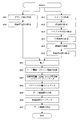
- FIG. 1 is a flowchart illustrating a manufacturing process of a thin film transistor according to an embodiment.
- 2 to 13 are diagrams showing a manufacturing process of the thin film transistor and a diagram for explaining the manufacturing process.
- Steps S01 and S02 are steps on the substrate side
- steps S11 to S16 are steps for forming a laminated film on the stamp side.
- the process on the substrate side and the process on the stamp side merge at the transfer process in step S21.
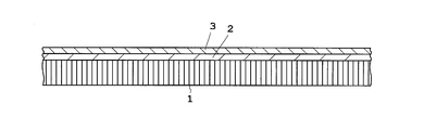
- a ground layer 2 is formed on almost the entire surface of the substrate 1.
- Al is used as the material of the ground layer 2.
- the ground layer 2 is not limited to Al, and may be a conductive material such as Ni (nickel) or ITO (indium tin oxide).
- the ground layer 2 is formed by a sputtering method, a vacuum deposition method, an ion plating method, a PECVD method, a printing method, or the like. Note that “substantially the entire surface” means that, for example, the ground layer 2 may not be formed on a part of the outer peripheral portion of the substrate 1.
- the material of the substrate glass, synthetic resin, Al (aluminum), SUS (stainless steel), graphite, or the like is used.
- PI polyimide
- PEN polyethylene naphthalate
- PES polyether sulfone
- PET polyethylene terephthalate
- the ground layer 2 may be omitted.
- connection conductive layer (metal layer) 3 is formed on almost the entire surface of the substrate 1. That is, the connection conductive layer 3 is formed on almost the entire surface of the substrate 1 on which the ground layer 2 is formed.
- Au gold
- the material of the connection conductive layer 3 is not limited to Au, and may be a conductive material such as Ag (silver).
- the connection conductive layer 3 is formed by a sputtering method, a vacuum deposition method, an ion plating method, a PECVD method, a printing method, or the like. “Substantially the entire surface” means that, for example, the connection conductive layer 3 may not be formed in a part of the outer peripheral portion of the substrate 1.
- the connection conductive layer 3 corresponds to the second conductive layer of the present invention.
- stamp 4 for transfer printing is formed.
- the stamp 4 is made of a flexible material having a good surface releasability, for example, a silicone resin such as PDMS (Polydimethylsiloxane).
- a silicone resin such as PDMS (Polydimethylsiloxane).
- the stamp 4 is manufactured by coating the original plate 5 having a concavo-convex pattern with a silicone resin and curing it, and then removing it from the original plate 5 as shown in FIG. 3B.
- the stamp 4 has a thickness of about 100 ⁇ m and an area on the front or back side of about A4 size.
- the height of the concavo-convex portion is about 1 ⁇ m to 10 ⁇ m.
- Step S12 Formation of Conductive Layer
- a conductive layer (metal layer) 6 is formed on the uneven pattern surface 4a of the stamp 4 on which the uneven pattern is formed.
- the conductive layer 6 is formed in contact with the lowermost layer of the laminated film 11 formed in steps S12 to S16, that is, the stamp 4. Thereby, it is possible to easily release the laminated film 11 from the stamp 4 during the transfer in step S21.
- Au is used as the material of the conductive layer 6. Further, the conductive layer 6 is not limited to Au, and other conductive materials may be used as long as the releasability from the stamp 4 is good.
- the conductive layer 6 may be omitted.
- the conductive layer 6 is formed by sputtering, vacuum deposition, ion plating, PECVD, or the like.
- the barrier metal layer 7, the semiconductor layer 8, the insulating film layer 9, and the connection conductive layer formed in steps S13 to S16 are similarly formed by sputtering, vacuum deposition, ion plating, PECVD, or the like.
- the conductive layer 6 corresponds to the third conductive layer of the present invention.
- Step S13 Formation of Barrier Metal Layer
- a barrier metal layer 7 is formed on the conductive layer 6 formed on the concavo-convex pattern surface 4a of the stamp 4.
- the barrier metal layer 7 is provided to improve the adhesion and conductivity between the semiconductor layer 8 and the conductive layer 6 formed in step S14. Further, the barrier metal layer 7 has an effect of preventing metal diffusion and mutual reaction depending on the material of the semiconductor layer 8 and the conductive layer 6.
- Mo mobdenum
- the material of the barrier metal layer 7 is not limited to Mo, and Ti (titanium), W (tungsten), or the like, or a compound containing them may be used. Further, when the semiconductor layer 8 described later is other than IGZO, the barrier metal layer 7 may not be formed as necessary.
- Step S14 Formation of Semiconductor Layer
- a semiconductor layer 8 is formed on the barrier metal layer 7 formed on the uneven pattern surface 4a of the stamp 4.
- an oxide semiconductor having at least one of In (indium), Ga (gallium), and Zn (zinc), for example, IGZO (InGaZnO 4 ) is used.
- the material of the semiconductor layer 8 may be ZnO (zinc oxide) other than IGZO as an oxide semiconductor.
- the material of the semiconductor layer 8 may be an organic semiconductor such as pentacene, a Si-based semiconductor such as a-Si (amorphous silicon), or a carbon nanotube.
- insulating layer 9 is formed on the semiconductor layer 8 formed on the uneven pattern surface 4a of the stamp 4.
- SiO 2 silicon dioxide
- the material of the insulating layer 9 is not limited to SiO 2, and may be SiN (silicon nitride), TiO 2 (titanium oxide), Al 2 O 3 (alumina), or PI (polyimide).
- an organic insulating layer 9 such as acrylic resin may be used.
- connection Conductive Layer 10 is formed on the insulating layer 9 formed on the uneven pattern surface 4a of the stamp 4.
- the connection conductive layer 10 is formed on the uppermost layer of the laminated film 11 formed in steps S12 to S16.
- Au is used as the material of the connection conductive layer 10.
- the material of the connection conductive layer 10 is not limited to Au, and may be a conductive material such as Ag.
- the connection conductive layer 10 corresponds to the first conductive layer of the present invention.
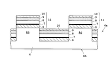
- the laminated film 11 is formed on the concave / convex pattern surface 4a of the stamp 4 in the order of the conductive layer 6, the barrier metal layer 7, the semiconductor layer 8, the insulating layer 9, and the connection conductive layer 10.
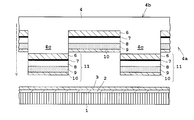
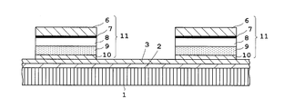
- Step S21 Transfer Before forming the gate electrode 31 in Step S27, which will be described later, on the substrate 1, by pressing the stamp 4 with gas from the opposite surface (back surface) 4b of the concavo-convex pattern surface 4a, The laminated film 11 of the stamp 4 is transferred to the substrate 1. Joining is performed by cold welding. As shown in FIG. 5, the uppermost connection conductive layer 10 of the laminated film 11 formed on the stamp 4 is opposed to the connection conductive layer 3 formed on the substrate 1. Next, the stamp 4 is placed on the substrate 1. Thereby, the connection conductive layer 10 of the stamp 4 and the connection conductive layer 3 of the substrate 1 come into contact with each other.
- connection conductive layer 3 is formed on almost the entire surface of the substrate 1, it is not necessary to accurately position the laminated film 11 formed on the convex portion 4 c of the stamp 4. That is, as shown in FIG. 15, it is not necessary to accurately position the semiconductor layer 115 and the insulating layer 116 formed on the stamp 114 on the gate electrode 112 formed on the substrate 111.
- the back surface 4b of the stamp 4 is pressurized with compressed air (gas).
- compressed air gas
- the substrate 1 is supported on a support base 15 in the chamber 13, and the stamp 4 is placed on the substrate 1 with the uneven pattern surface 4 a of the stamp 4 facing the substrate 1.
- the compressed air is compressed by power such as a pump (not shown) and supplied from a supply port 17 provided in the chamber 13.
- the compressed air in the chamber 13 is exhausted from the exhaust port 19.
- the compressed air is air or an inert gas such as N 2 (nitrogen) or Ar (argon).
- the pressurization causes the space 21 in the chamber 13 to be, for example, 0.4 MPa (4 atm).
- the pressure in the space 23 surrounded by the stamp 4 and the substrate 1 is, for example, 0.1 MPa (1 atm).
- the space 23 is sealed with the stamp 4 and the substrate 1. That is, the stamp 4 is pressed against the substrate 1 by the pressure difference between the space 21 and the space 23.
- the inside of the chamber 13 is, for example, normal temperature (20 ⁇ 15 ° C.).
- the state where the connection conductive layer 10 of the stamp 4 and the connection conductive layer 3 of the substrate 1 are in contact, that is, the pressurized state is continued for 6 to 12 hours.
- the pressurization time depends on the pressure and temperature in the chamber 13.
- connection conductive layer 10 of the stamp 4 and the connection conductive layer 3 of the substrate 1 are both made of Au.
- the Au layer and the Au layer are naturally fused and joined (cold-welding) by a preset pressure (for example, 0.4 MPa). Then, after the pressurizing time has elapsed, the laminated film 11 is peeled from the stamp 4 by separating the stamp 4 from the substrate 1 (FIG. 7). Note that the surfaces of the connection conductive layer 10 of the stamp 4 and the connection conductive layer 3 of the substrate 1 may be cleaned by Ar plasma treatment or UV irradiation before transfer.
- the source electrode 25 and the drain electrode 27 are formed on the laminated film 11 by a printing method.
- the source electrode 25 and the drain electrode 27 are formed by printing metal ink such as Ag or Cu (copper) with an ink jet printer (ink jet method).
- the printing method is not limited to the ink jet method, and a relief printing method, an intaglio printing method such as gravure printing, a lithographic printing method such as offset printing, a screen printing method, or the like may be used.
- the metal ink is cured by standing at room temperature, heating, or UV irradiation.
- Au may be used as the material for the source electrode 25 and the drain electrode 27.
- connection Conductive Layer (Substrate) and Conductive Layer (Stamp) Referring to FIG.
- the connection conductive layer 3 and the conductive layer 6 are wet etched using the source electrode 25 and the drain electrode 27 as a mask.
- an iodine-based gold etching solution for example, AURUM, manufactured by Kanto Chemical Co., Inc.
- the source electrode 25 and the drain electrode 27 serve as a mask, and Au of the connection conductive layer 3 and the conductive layer 6 other than the portion covered with the source electrode 25 and the drain electrode 27 is removed.
- connection conductive layer 3 when the connection conductive layer 3 is made of Ag and the conductive layer 6 is made of Au, the connection conductive layer 3 may be removed using the conductive layer 6, the source electrode 25, and the drain electrode 27 as a mask. In this case, it is preferable that the connection conductive layer 3 is made of a material different from that of the conductive layer 6, the source electrode 25, and the drain electrode 27. That is, in this step, the conductive layer 6 other than the portions covered with the source electrode 25 and the drain electrode 27 is removed, and the connection conductive layer 3 portion not bonded to the laminated film 11 is removed.
- Step S24 Etching of Barrier Metal Layer
- the barrier metal layer 7 is wet etched using the source electrode 25 and the drain electrode 27 as a mask.
- the barrier metal layer 7 is made of Mo
- hydrogen peroxide water (H 2 O 2 ) is used for the etching.
- the etching removes the barrier metal layer 7 other than the portion covered with the source electrode 25 and the drain electrode 27.
- a gate insulating film 29 is formed on the semiconductor layer 8 by a printing method.
- the gate insulating film 29 is formed by an ink jet printer (ink jet method).
- the printing method is not limited to the ink jet method, and a relief printing method, an intaglio printing method such as gravure printing, a lithographic printing method such as offset printing, a screen printing method, or the like may be used.
- the gate insulating film 29 is cured by standing at room temperature, heating, or UV irradiation.
- the gate insulating film 29 may be formed by SAM (Self-Assembled Monolayer).
- the substrate 1 obtained in the steps up to step S24 described above is immersed in a solution of organic molecules having an affinity for the semiconductor layer 8. Then, organic molecules are chemisorbed on the surface of the semiconductor layer 8 to form an organic thin film (that is, the gate insulating film 29).
- Step S26 Etching of Semiconductor Layer
- the semiconductor layer 8 is wet-etched using the source electrode 25, the drain electrode 27, and the gate insulating film 29 as a mask.
- etching for example, when the semiconductor layer 8 is made of IGZO, hydrochloric acid (HCl) is used.
- HCl hydrochloric acid
- Step S27 Formation of Gate Electrode A gate electrode 31 is formed on the gate insulating film 29.
- the gate electrode 31 is formed by printing a metal ink such as Au, Ag, or Cu with an ink jet printer (ink jet method).
- the printing method is not limited to the ink jet method, and a relief printing method, an intaglio printing method such as gravure printing, a lithographic printing method such as offset printing, a screen printing method, or the like may be used.
- the metal ink is cured by standing at room temperature, heating, or UV irradiation.
- the TFT 33 is formed by the above manufacturing method. As shown in FIG. 13, for example, an insulating film 35 of PI is formed between the plurality of TFTs 33. On the insulating film 35, a gate line (not shown) for transmitting a signal to the gate electrode 31 and a data line (not shown) for reading data are formed. A capacitor (not shown) is formed for each TFT 33. Note that the gate line, the data line, and the capacitor correspond to the gate line 104, the data line 106, and the capacitor 101 shown in FIG.
- the laminated film 11 is formed in the order of the semiconductor layer 8 and the insulating layer 9 on the concavo-convex pattern surface 4a of the stamp 4 on which the concavo-convex pattern is formed.
- a connection conductive layer 10 is formed on the uppermost layer of the film 11.
- the connection conductive layer 3 is formed on almost the entire surface of the substrate 1.
- the stamp 4 is pressed from the surface 4 b on the opposite side of the concavo-convex pattern surface 4 a to form the connection conductive layer 10 formed on the stamp 4 and the substrate 1.
- the connection conductive layer 3 is joined.
- connection conductive layer 3 is formed on almost the entire surface of the substrate 1, when the stamp 4 is placed on the substrate 1, the connection conductive layer 10 formed on the stamp 4 and the substrate 1 are formed. The connection conductive layer 10 and the connection conductive layer 3 are joined at an arbitrary position where the connection conductive layer 3 is in contact. Further, before forming the gate electrode 31 on the substrate 1, the laminated film 11 including the semiconductor layer 8 and the insulating film 9 is transferred to the substrate 1. Accordingly, it is possible to eliminate the need for accurate alignment at the time of transfer using the stamp 4.
- connection conductive layer 10 and the connection conductive layer 3 are formed on the bonding surface. If the connection conductive layer 10 and the connection conductive layer 3 are made of a noble metal such as Au, contamination is hardly attached essentially. Even if contamination adheres, it is possible to bond even under atmospheric pressure (outside the vacuum chamber) by cleaning with UV ozone irradiation method before bonding. That is, transfer can be easily performed without using an expensive vacuum apparatus. Moreover, since the laminated film 11 is sandwiched between the conductive layer 6 and the connection conductive layer 10, the semiconductor film 8 can be prevented from being contaminated.
- the stamp 4 when a member is pressed from the surface (back surface) 4b opposite to the concave / convex pattern surface 4a of the stamp 4, pressure is applied within the contact surface between the member and the stamp 4 depending on the surface shape of the member. Variation will occur.
- the back surface 4b of the stamp 4 with gas, for example, the plurality of laminated films 11 formed on the convex portions 4c arranged in an array of the stamp 4 and the substrate 1 can be uniformly pressed within the contact surface. it can.
- the stamp when the stamp becomes high temperature, it deforms due to thermal expansion. However, deterioration of dimensional accuracy due to deformation of the stamp can be suppressed by applying pressure at low temperature welding (cold welding), for example, at room temperature.
- cold welding low temperature welding
- the barrier metal layer 7 can improve the adhesion and conductivity between the semiconductor layer 8 and the connection conductive layer 6 as compared with the case where the connection conductive layer 6 is formed directly on the semiconductor layer 8. It also has the effect of preventing metal diffusion and preventing mutual reaction. By forming the connection conductive layer 6 in the lowermost layer of the laminated film 11, the releasability between the stamp 4 and the laminated film 11 can be improved.
- the ground layer is formed in the same height as the gate line.
- the resistance of the ground layer becomes high, and the ground layer itself becomes a source of thermal noise and is easily affected by external noise. For this reason, artifacts are generated in the acquired image.
- the resistance can be lowered and noise can be suppressed. Thereby, an artifact can be suppressed.
- the pixel area pixel pitch
- the ground layer 2 can shield the back gate of the TFT 33 from external noise (electromagnetic waves). The ground layer 2 can prevent water vapor and oxygen from passing therethrough.
- the source electrode 25 and the drain electrode 27 can be easily formed on the laminated film 11 by a printing method. Further, since etching can be performed using the source electrode 25 and the drain electrode 27 as a mask, it is not necessary to form a resist film, for example, and the manufacture of the TFT 33 can be facilitated.
- the gate insulating film 29 and the gate electrode 31 are formed in this order on the semiconductor layer 8 by the printing method. Thereby, a top gate type TFT 33 can be manufactured.
- the gate electrode 31 is formed after the laminated film 11 is transferred, the gate electrode 31 is formed in accordance with the laminated film 11 that has been misaligned and transferred even if the laminated film 11 is misaligned and transferred. can do.
- the semiconductor layer and the insulating layer of the stamp are transferred in precise alignment with the gate electrode.
- the stamp 4 is made of a soft material, misalignment occurs in other parts even if the part 4 is accurately aligned.
- the gate electrode 31 since the gate electrode 31 is formed after the semiconductor layer 8 and the insulating layer 9 are transferred, it is possible to suppress a decrease in the yield of the TFT 33 due to the transfer of the stamp 4.
- the present invention is not limited to the above embodiment, and can be modified as follows.
- the convex portion 4c of the stamp 4 may be formed in a one-dimensional or two-dimensional array.
- the thin film transistor (TFT) 31 is formed in a one-dimensional or two-dimensional array.
- connection conductive layer 10 made of Au of the stamp 4 and the connection conductive layer 3 made of Au of the substrate 1 are joined by low-temperature welding. That is, the Au layer and the Au layer are joined.
- the Ag layer and the Ag layer may be joined, or the Au layer and the Ag layer, or the Ag layer and the Au layer may be joined.
- the barrier metal layer 7, the semiconductor layer 8, and the insulating layer 9 may be composed of multiple layers.
Landscapes
- Thin Film Transistor (AREA)
- Electrodes Of Semiconductors (AREA)
Abstract
薄膜トランジスタ(TFT)の製造方法は、基板1上の全面に接続導電層3を形成しているので、スタンプ4を基板1上に載置した際に、スタンプ4に形成された接続導電層10と、基板1上に形成された接続導電層3とが接触した任意の位置で、接続導電層10と接続導電層3とが接合される。また、基板1にゲート電極を形成する前に、基板1に半導体層8および絶縁膜9を含む積層膜11が転写される。したがって、スタンプ4による転写時における正確な位置合わせを不要とすることができる。
Description
本発明は、コンピュータの出力装置やテレビなどに用いられる薄型ディスプレイ(例えば液晶ディスプレイ)や、放射線(例えばX線やγ線や赤外線等の光)を検出するフラットパネル型放射線検出器に設けられる、アレイ状に形成される薄膜トランジスタの製造方法に関する。
従来、薄型ディスプレイやフラットパネル型放射線検出器には、二次元アレイ状(二次元マトリクス状)の画素ごとにコンデンサと薄膜トランジスタ(thin film transistor)が設けられている。なお、薄膜トランジスタは、以下適宜「TFT」と略される。例えば、フラットパネル型放射線検出器を一例に構成および動作を説明する。
図14を参照する。まず、コンデンサ101には、入射した放射線を電荷に変換する変換層102により、放射線の強度に応じた電荷が蓄積される。TFT103のゲート電極は、水平方向の列ごとにゲート線104が接続され、ゲート線104は、ゲート駆動回路105に接続されている。また、TFT103のコンデンサ101と接続される反対側の端子には、垂直方向の列ごとにデータ線106が接続されている。ゲート駆動回路105は、ゲート線104に順次、駆動信号を発信することにより、二次元アレイ状の画素の水平方向の列ごとにTFT103のゲートがON状態になる。これにより、コンデンサ101に蓄積された電荷が読み出される。すなわち各画素の電荷(検出信号)を読み出して、画像を取得している。
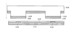
このような二次元アレイ状に形成されるTFT103の製造方法は、図15に示すように、まず、基板111上にゲート電極112を形成し、硬化されていない接着膜(絶縁膜)113を形成する。そして、スタンプ114の凹凸パターン面には、半導体層115と絶縁層116とが形成され、硬化されていない接着膜113上に半導体層115と絶縁層116とを転写させ、接着膜113を硬化させる。この後、図16に示すように、レジスト膜117をマスクとして半導体層115を低抵抗化させる処理を行う。なお、未処理の半導体層部分を符号115aで示し、低抵抗化された半導体層部分を符号115bで示す。低抵抗化された半導体層部分115b上にソース電極118とドレイン電極119とを形成する。このようにして、TFT103をボトムゲート型に形成している(例えば特許文献1参照)。
なお、引用文献2には、次の方法が開示されている。まず、スタンプに転写材料を接続させる。次に、その転写材料を硬化されていない液体状の樹脂膜(接着膜)に接触させ、樹脂膜を硬化させる。そして、転写材料をスタンプから剥離する。これにより、スタンプを用いて基板上に転写材料を転写させている。
特開2010-267719号公報
特表2009-508322号公報
しかしながら、硬化させる前の液体状の樹脂膜に転写材料を接触させ、接触後に樹脂膜を硬化させる場合、硬化した樹脂膜の膜厚が不均一になる。これは、スタンプに接続された転写材料が、液体状の樹脂膜中に沈む程度により、樹脂膜の膜厚が不均一になるからである。この状態で、樹脂膜を硬化させるので、硬化後の樹脂膜に対する膜厚の制御は困難なものとなる。
さらに硬化した樹脂膜をゲート絶縁膜として利用する場合、薄膜トランジスタごとにゲート絶縁膜の膜厚にバラツキが生じる。ゲート絶縁膜の膜厚が不均一になると、薄膜トランジスタのゲート容量にバラツキを発生させ、薄膜トランジスタのON/OFF特性のバラツキの原因となる問題が生じる。
この問題に対して本出願人は、特願2010-171978号により次のような方法を提案している。図15を参照する。基板111上に接着膜113を形成し、硬化させる。また、硬化させた接着膜113に対してアルゴンプラズマ処理または酸素プラズマ処理を実施する。一方、スタンプ114の凹凸パターン面に半導体層115と絶縁層116を形成し、絶縁層116に対してアルゴンプラズマ処理または酸素プラズマ処理を実施する。そして、接着膜113と絶縁層117とを接触させ、接着膜113と絶縁層117との接触面において生じる脱水縮合反応により、接着膜113と絶縁層117とを接合させている。これにより、スタンプ114に形成された半導体層115と絶縁層116を、基板111上の接着膜113に転写させている。接着膜113は硬化されているので、接着膜113の膜厚の不均一を低減させることができる。
しかしながら、このような薄膜トランジスタの製造方法には、さらに次のような問題がある。すなわち、図15および図16に示すように、薄膜トランジスタは、ボトムゲート型である。そのため、スタンプ114の凹凸パターン側に形成された半導体層115および絶縁層116を、基板111上のゲート電極112上に転写するために接触させる際に、スタンプ114の凸部を、ゲート電極112上に正確に位置合わせする必要がある。結果として、転写するための装置が位置合わせ機能を備えた高額なものにならざるを得なかった。
本発明は、このような事情に鑑みてなされたものであって、スタンプによる転写時における正確な位置合わせを不要とした薄膜トランジスタの製造方法を提供することを目的とする。
本発明は、このような目的を達成するために、次のような構成をとる。すなわち、本発明の薄膜トランジスタの製造方法は、凹凸パターンが形成されたスタンプの凹凸パターン面に半導体層、絶縁層の順番で積層膜を形成する工程と、前記スタンプに形成される前記積層膜の最上層に第1導電層を形成する工程と、基板上の全面に第2導電層を形成する工程と、前記基板にゲート電極を形成する前に、前記凹凸パターン面の反対側の面から前記スタンプを加圧して前記第1導電層と前記第2導電層とを接合させることにより、前記基板に前記スタンプの積層膜を転写する工程と、を備えているものである。
本発明に係る薄膜トランジスタの製造方法によれば、凹凸パターンが形成されたスタンプの凹凸パターン面に、半導体層、絶縁層の順番で積層膜を形成し、その積層膜の最上層に、第1導電層を形成する。一方、基板上の全面に第2導電層を形成する。そして、基板にゲート電極を形成する前に、凹凸パターン面の反対側の面からスタンプを加圧して、スタンプに形成された第1導電膜と、基板に形成された第2導電層とを接合させる。これにより、基板に積層膜が転写される。基板上の全面に第2導電層を形成しているので、スタンプを基板上に載置した際に、スタンプに形成された第1導電層と、基板上に形成された第2導電層とが接触した任意の位置で、第1電導層と第2電導層とが接合される。また、基板にゲート電極を形成する前に、基板に半導体層および絶縁膜を含む積層膜が転写される。したがって、スタンプによる転写時における正確な位置合わせを不要とすることができる。
また、本発明の薄膜トランジスタの製造方法は、前記転写する工程は、前記スタンプを気体で加圧することが好ましい。例えば、スタンプの凹凸パターン面と反対側の面(背面)から部材を押し当てて加圧する場合、その部材の表面形状等により、部材とスタンプとの接触面内で加圧にばらつきが生じてしまう。スタンプの背面を気体で加圧することにより、例えば、スタンプのアレイ状に配置した凸部に形成された複数の積層膜と基板とを接触面内で均一に加圧することができる。
また、本発明の薄膜トランジスタの製造方法において、前記転写する工程は、前記スタンプを常温で加圧することが好ましい。スタンプが高温になると熱膨張により変形するが、常温で加圧することにより、スタンプの変形による寸法精度の悪化を抑えることができる。
また、本発明の薄膜トランジスタの製造方法において、前記積層膜は、前記スタンプの凹凸パターン面にバリアメタル層、半導体層、絶縁層の順番で形成されていることが好ましい。バリアメタル層、半導体層の順番に形成すること、すなわち、バリアメタル層を半導体層に接して形成することにより次の効果を有する。バリアメタル層は、半導体層に直接、導電性の層を形成する場合よりも、半導体層と導電性の層における密着性および導電率を良くすることができる。また、金属拡散防止や相互反応防止の効果も有する。
また、本発明の薄膜トランジスタの製造方法は、前記スタンプに形成される前記積層膜の最下層に第3導電層を形成する工程を備えていることが好ましい。積層膜の最下層に第3導電層を形成することにより、スタンプと積層膜との離型性を良くすることができる。
また、本発明の薄膜トランジスタの製造方法は、前記第2導電層を形成する前に、前記基板上の全面にグランド層を形成する工程を備えていることが好ましい。ボトムゲートの薄膜トランジスタの構成では、グランド層は、ゲート線と同じ高さの層に形成される。グランド層が線として細く形成される場合、グランド層の抵抗が高くなり、ノイズが生じる。そのため、取得される画像にアーチファクトを生じさせていた。しかしながら、基板上の全面にグランド層を形成することで、抵抗を低くすることができ、ノイズを抑えることができる。これにより、アーチファクトを抑えることができる。
また、本発明の薄膜トランジスタの製造方法は、前記転写する工程の後に、前記積層膜上にソース電極およびドレイン電極を印刷法により形成する工程を備えていることが好ましい。これにより、積層膜上にソース電極およびドレイン電極を容易に形成することができる。
また、本発明の薄膜トランジスタの製造方法は、前記ソース電極および前記ドレイン電極をマスクとして前記第2導電層、前記第3導電層および前記バリアメタル層の少なくとも1つの層をエッチングする工程を備えていることが好ましい。ソース電極およびドレイン電極をマスクとしてエッチングすることができるので、例えばレジスト膜を形成しなくてもよく、薄膜トランジスタの製造を容易にすることができる。
また、本発明の薄膜トランジスタの製造方法は、前記転写する工程の後に、前記半導体層上にゲート絶縁膜、前記ゲート電極の順番で前記ゲート絶縁膜および前記ゲート電極を印刷法により形成する工程を備えていることが好ましい。これにより、トップゲート型の薄膜トランジスタを製造することができる。また、積層膜を転写した後にゲート電極を形成しているので、積層膜が位置ズレして転写されても、位置ズレして転写された積層膜に合わせてゲート電極を形成することができる。そのため、スタンプの転写による薄膜トランジスタの歩留まりの低下を抑えることができる。
本発明に係る薄膜トランジスタの製造方法によれば、凹凸パターンが形成されたスタンプの凹凸パターン面に、半導体層、絶縁層の順番で積層膜を形成し、その積層膜の最上層に、第1導電層を形成する。一方、基板上の全面に第2導電層を形成する。そして、基板にゲート電極を形成する前に、凹凸パターン面の反対側の面からスタンプを加圧して、スタンプに形成された第1導電膜と、基板に形成された第2導電層とを接合させる。これにより、基板に積層膜が転写される。基板上の全面に第2導電層を形成しているので、スタンプを基板上に載置した際に、スタンプに形成された第1導電層と、基板上に形成された第2導電層とが接触した任意の位置で、第1電導層と第2電導層とが接合される。また、基板にゲート電極を形成する前に、基板に半導体層および絶縁膜を含む積層膜が転写される。したがって、スタンプによる転写時における正確な位置合わせを不要とすることができる。
1 … 基板
2 … グランド層
3 … 接続電導層
4 … スタンプ
6 … 導電層
7 … バリアメタル層
8 … 半導体層
9 … 絶縁層
10 … 接続導電層
11 … 積層膜
13 … チャンバ
15 … 支持台
17 … 供給口
25 … ソース電極
27 … ドレイン電極
29 … ゲート絶縁膜
31 … ゲート電極
33 … 薄膜トランジスタ(TFT)
2 … グランド層
3 … 接続電導層
4 … スタンプ
6 … 導電層
7 … バリアメタル層
8 … 半導体層
9 … 絶縁層
10 … 接続導電層
11 … 積層膜
13 … チャンバ
15 … 支持台
17 … 供給口
25 … ソース電極
27 … ドレイン電極
29 … ゲート絶縁膜
31 … ゲート電極
33 … 薄膜トランジスタ(TFT)
以下、図面を参照して本発明の実施例を説明する。図1は、実施例に係る薄膜トランジスタの製造工程を示すフローチャートである。図2~図13は、薄膜トランジスタの製造工程を示す図、および製造工程の説明に供する図である。
まず、図1のフローチャートに沿って薄膜トランジスタ(TFT)の製造方法を説明する。図1を参照する。ステップS01,S02は基板側の工程であり、ステップS11~S16はスタンプ側の積層膜を形成する工程である。基板側の工程およびスタンプ側の工程は、ステップS21の転写の工程で合流する。
〔ステップS01〕グランド層の形成
図2を参照する。基板1上のほぼ全面にグランド層2を形成する。グランド層2の材料は、Alが用いられる。また、グランド層2は、Alに限定されず、Ni(ニッケル)やITO(酸化インジウムスズ)等の導電性材料であってもよい。グランド層2は、スパッタリング法、真空蒸着法、イオンプレーティング法、PECVD法、印刷法等で形成される。なお、「ほぼ全面」とは、例えば、基板1の外周部の一部でグランド層2が形成されていなくてもよい。
図2を参照する。基板1上のほぼ全面にグランド層2を形成する。グランド層2の材料は、Alが用いられる。また、グランド層2は、Alに限定されず、Ni(ニッケル)やITO(酸化インジウムスズ)等の導電性材料であってもよい。グランド層2は、スパッタリング法、真空蒸着法、イオンプレーティング法、PECVD法、印刷法等で形成される。なお、「ほぼ全面」とは、例えば、基板1の外周部の一部でグランド層2が形成されていなくてもよい。
また、基板1の材料は、ガラス、合成樹脂、Al(アルミニウム)、SUS(ステンレス)およびグラファイト等が用いられる。合成樹脂の場合は、PI(ポリイミド)、PEN(ポリエチレンナフタレート)、PES(ポリエーテルスルホン)、PET(ポリエチレンテレフタレート)等が用いられる。なお、例えばAl、SUSやグラファイト等の導電性材料で基板1が構成される場合は、グランド層2を省略してもよい。
〔ステップS02〕接続導電層の形成
基板1上のほぼ全面に接続電導層(金属層)3を形成する。すなわち、グランド層2が形成された基板1上のほぼ全面に接続導電層3を形成する。接続導電層3の材料は、Au(金)が用いられる。また、接続導電層3の材料は、Auに限定されず、Ag(銀)等の導電性材料であってもよい。接続導電層3は、スパッタリング法、真空蒸着法、イオンプレーティング法、PECVD法、印刷法等で形成される。「ほぼ全面」とは、例えば、基板1の外周部の一部で接続導電層3が形成されていなくてもよい。接続導電層3は、本発明の第2導電層に相当する。
基板1上のほぼ全面に接続電導層(金属層)3を形成する。すなわち、グランド層2が形成された基板1上のほぼ全面に接続導電層3を形成する。接続導電層3の材料は、Au(金)が用いられる。また、接続導電層3の材料は、Auに限定されず、Ag(銀)等の導電性材料であってもよい。接続導電層3は、スパッタリング法、真空蒸着法、イオンプレーティング法、PECVD法、印刷法等で形成される。「ほぼ全面」とは、例えば、基板1の外周部の一部で接続導電層3が形成されていなくてもよい。接続導電層3は、本発明の第2導電層に相当する。
〔ステップS11〕スタンプの形成
転写印刷用のスタンプ4を形成する。スタンプ4は、柔軟性があり表面の離型性のよい材料、例えばPDMS(Polydimethylsiloxane)などのシリコーン樹脂で構成される。スタンプ4は、図3(a)に示すように、凹凸パターンを有する原版5にシリコーン樹脂をコーティングして硬化させ、図3(b)に示すように、原版5から剥離することで作製される。スタンプ4は、例えば、厚みが100μm程で、前面または背面側の面積がA4サイズ程度の大きさである。また凹凸部の高さは、約1μm~10μm程である。
転写印刷用のスタンプ4を形成する。スタンプ4は、柔軟性があり表面の離型性のよい材料、例えばPDMS(Polydimethylsiloxane)などのシリコーン樹脂で構成される。スタンプ4は、図3(a)に示すように、凹凸パターンを有する原版5にシリコーン樹脂をコーティングして硬化させ、図3(b)に示すように、原版5から剥離することで作製される。スタンプ4は、例えば、厚みが100μm程で、前面または背面側の面積がA4サイズ程度の大きさである。また凹凸部の高さは、約1μm~10μm程である。
〔ステップS12〕導電層の形成
図4を参照する。凹凸パターンが形成されたスタンプ4の凹凸パターン面4aに導電層(金属層)6を形成する。ステップS12~S16で形成される積層膜11の最下層、すなわち、スタンプ4に接して導電層6を形成する。これにより、ステップS21の転写時の際に、スタンプ4から積層膜11を離型させ易くすることができる。導電層6の材料は、Auが用いられる。また、導電層6は、Auに限定されず、スタンプ4との離型性が良ければ他の導電性材料を用いてもよい。また、例えば、ステップS13で形成されるバリアメタル層7がスタンプ4との離型性が良いときは、導電層6を省略してもよい。導電層6は、スパッタリング法、真空蒸着法、イオンプレーティング法、PECVD法等で形成される。なお、ステップS13~S16で形成されるバリアメタル層7、半導体層8、絶縁膜層9、接続導電層も同様に、スパッタリング法、真空蒸着法、イオンプレーティング法、PECVD法等で形成される。また、導電層6は、本発明の第3導電層に相当する。
図4を参照する。凹凸パターンが形成されたスタンプ4の凹凸パターン面4aに導電層(金属層)6を形成する。ステップS12~S16で形成される積層膜11の最下層、すなわち、スタンプ4に接して導電層6を形成する。これにより、ステップS21の転写時の際に、スタンプ4から積層膜11を離型させ易くすることができる。導電層6の材料は、Auが用いられる。また、導電層6は、Auに限定されず、スタンプ4との離型性が良ければ他の導電性材料を用いてもよい。また、例えば、ステップS13で形成されるバリアメタル層7がスタンプ4との離型性が良いときは、導電層6を省略してもよい。導電層6は、スパッタリング法、真空蒸着法、イオンプレーティング法、PECVD法等で形成される。なお、ステップS13~S16で形成されるバリアメタル層7、半導体層8、絶縁膜層9、接続導電層も同様に、スパッタリング法、真空蒸着法、イオンプレーティング法、PECVD法等で形成される。また、導電層6は、本発明の第3導電層に相当する。
〔ステップS13〕バリアメタル層の形成
スタンプ4の凹凸パターン面4aに形成された導電層6上にバリアメタル層7を形成する。バリアメタル層7は、ステップS14で形成される半導体層8と導電層6との間における密着性および導電率を良くするために設けられる。さらにバリアメタル層7は、半導体層8や導電層6の材料により、金属拡散防止や相互反応防止の効果を有する。バリアメタル層7の材料は、後述する半導体層8がIGZOの場合、Mo(モリブデン)が用いられる。また、バリアメタル層7の材料は、Moに限定されず、Ti(チタン)、W(タングステン)等、またはそれらを含む化合物であってもよい。また、後述する半導体層8がIGZO以外の場合は、必要に応じてバリアメタル層7を形成しなくともよい。
スタンプ4の凹凸パターン面4aに形成された導電層6上にバリアメタル層7を形成する。バリアメタル層7は、ステップS14で形成される半導体層8と導電層6との間における密着性および導電率を良くするために設けられる。さらにバリアメタル層7は、半導体層8や導電層6の材料により、金属拡散防止や相互反応防止の効果を有する。バリアメタル層7の材料は、後述する半導体層8がIGZOの場合、Mo(モリブデン)が用いられる。また、バリアメタル層7の材料は、Moに限定されず、Ti(チタン)、W(タングステン)等、またはそれらを含む化合物であってもよい。また、後述する半導体層8がIGZO以外の場合は、必要に応じてバリアメタル層7を形成しなくともよい。
〔ステップS14〕半導体層の形成
スタンプ4の凹凸パターン面4aに形成されたバリアメタル層7上に半導体層8を形成する。半導体層8の材料は、In(インジウム)、Ga(ガリウム)、Zn(亜鉛)を少なくとも1つを有する酸化物半導体、例えばIGZO(InGaZnO4)が用いられる。また、半導体層8の材料は、酸化物半導体としてIGZO以外にも、ZnO(酸化亜鉛)であってもよい。また、半導体層8の材料は、ペンタセン等の有機半導体、a-Si(アモルファスシリコン)等のSi系の半導体、あるいはカーボンナノチューブであってもよい。
スタンプ4の凹凸パターン面4aに形成されたバリアメタル層7上に半導体層8を形成する。半導体層8の材料は、In(インジウム)、Ga(ガリウム)、Zn(亜鉛)を少なくとも1つを有する酸化物半導体、例えばIGZO(InGaZnO4)が用いられる。また、半導体層8の材料は、酸化物半導体としてIGZO以外にも、ZnO(酸化亜鉛)であってもよい。また、半導体層8の材料は、ペンタセン等の有機半導体、a-Si(アモルファスシリコン)等のSi系の半導体、あるいはカーボンナノチューブであってもよい。
〔ステップS15〕絶縁層の形成
スタンプ4の凹凸パターン面4aに形成された半導体層8上に絶縁層9を形成する。絶縁層9の材料は、SiO2(二酸化ケイ素)が用いられる。また、絶縁層9の材料は、SiO2に限定されず、SiN(窒化シリコン)や、TiO2(酸化チタン)、Al2O3(アルミナ)、であってもよく、また、PI(ポリイミド)やアクリル系樹脂等の有機系の絶縁層9であってもよい。
スタンプ4の凹凸パターン面4aに形成された半導体層8上に絶縁層9を形成する。絶縁層9の材料は、SiO2(二酸化ケイ素)が用いられる。また、絶縁層9の材料は、SiO2に限定されず、SiN(窒化シリコン)や、TiO2(酸化チタン)、Al2O3(アルミナ)、であってもよく、また、PI(ポリイミド)やアクリル系樹脂等の有機系の絶縁層9であってもよい。
〔ステップS16〕接続導電層の形成
スタンプ4の凹凸パターン面4aに形成された絶縁層9上に接続導電層(金属層)10を形成する。ステップS12~S16で形成される積層膜11の最上層に接続導電層10を形成する。接続導電層10の材料は、Auが用いられる。また、接続導電層10の材料は、Auに限定されず、Ag等の導電性材料であってもよい。なお、接続導電層10は、本発明の第1導電層に相当する。
スタンプ4の凹凸パターン面4aに形成された絶縁層9上に接続導電層(金属層)10を形成する。ステップS12~S16で形成される積層膜11の最上層に接続導電層10を形成する。接続導電層10の材料は、Auが用いられる。また、接続導電層10の材料は、Auに限定されず、Ag等の導電性材料であってもよい。なお、接続導電層10は、本発明の第1導電層に相当する。
ステップS12~S16により、スタンプ4の凹凸パターン面4aには、導電層6、バリアメタル層7、半導体層8、絶縁層9、接続導電層10の順番で積層膜11が形成される。
〔ステップS21〕転写
後述するステップS27のゲート電極31を基板1に形成する前に、前記凹凸パターン面4aの反対側の面(背面)4bからスタンプ4を気体で加圧して接合させることにより、基板1にスタンプ4の積層膜11を転写する。接合は低温溶接(cold welding)で行われる。図5に示すように、スタンプ4に形成された積層膜11の最上層の接続導電層10と、基板1に形成された接続導電層3とが対向する状態とする。次に、スタンプ4を基板1に載置させる。これにより、スタンプ4の接続導電層10と基板1の接続導電層3とが接触する。このとき、接続導電層3は、基板1のほぼ全面に形成されているので、スタンプ4の凸部4cに形成された積層膜11の正確な位置決めを必要としなくてもよい。すなわち、図15に示すように、スタンプ114に形成された半導体層115および絶縁層116を、基板111に形成されたゲート電極112上に正確に位置決めすることを必要としない。
後述するステップS27のゲート電極31を基板1に形成する前に、前記凹凸パターン面4aの反対側の面(背面)4bからスタンプ4を気体で加圧して接合させることにより、基板1にスタンプ4の積層膜11を転写する。接合は低温溶接(cold welding)で行われる。図5に示すように、スタンプ4に形成された積層膜11の最上層の接続導電層10と、基板1に形成された接続導電層3とが対向する状態とする。次に、スタンプ4を基板1に載置させる。これにより、スタンプ4の接続導電層10と基板1の接続導電層3とが接触する。このとき、接続導電層3は、基板1のほぼ全面に形成されているので、スタンプ4の凸部4cに形成された積層膜11の正確な位置決めを必要としなくてもよい。すなわち、図15に示すように、スタンプ114に形成された半導体層115および絶縁層116を、基板111に形成されたゲート電極112上に正確に位置決めすることを必要としない。
スタンプ4を基板1に載置した後、図6に示すように、圧縮空気(気体)によりスタンプ4の背面4bを加圧する。具体的には、基板1は、チャンバ13内の支持台15に支持しておき、スタンプ4の凹凸パターン面4aを基板1に対向した状態で、スタンプ4が基板1に載置されている。圧縮空気は、図示しないポンプ等の動力により圧縮されて、チャンバ13内に設けられた供給口17から供給される。なお、チャンバ13内の圧縮空気は、排気口19から排気するようになっている。圧縮空気は、大気あるいは、N2(窒素)やAr(アルゴン)等の不活性ガスが用いられる。加圧は、チャンバ13内の空間21を、例えば0.4MPa(4気圧)にする。一方、スタンプ4と基板1とで囲まれた空間23の圧力が、例えば0.1MPa(1気圧)であるとする。なお、空間23は、スタンプ4と基板1とで密閉されている。すなわち、これら空間21と空間23との圧力差によりスタンプ4が基板1に加圧される。チャンバ13内は、例えば常温(20±15℃)である。スタンプ4の接続導電層10と基板1の接続導電層3とが接触した状態、すなわち加圧した状態は、6~12時間継続される。加圧時間は、チャンバ13内の圧力と温度に依存する。
スタンプ4の接続導電層10と基板1の接続導電層3は、共にAuで構成されていることが好ましい。Au層とAu層は、予め設定された圧力(例えば0.4MPa)により、自然に融合して接合される(cold welding)。そして、上述の加圧時間が経過した後、スタンプ4を基板1から離すことで、スタンプ4から積層膜11が剥離される(図7)。なお、転写前に、スタンプ4の接続導電層10と基板1の接続導電層3の表面を、Arプラズマ処理やUV照射でクリーニングしてもよい。
〔ステップS22〕ソース電極・ドレイン電極の形成
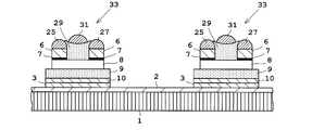
図8を参照する。ステップS21の転写する工程の後に、積層膜11上にソース電極25およびドレイン電極27を印刷法により形成する。ソース電極25およびドレイン電極27の材料は、AgまたはCu(銅)等が用いられる。ソース電極25およびドレイン電極27は、AgまたはCu(銅)等の金属インクをインクジェットプリンタ(インクジェット法)で印刷することにより形成される。また、印刷法は、インクジェット法に限定されず、凸版印刷法や、グラビア印刷等の凹版印刷法、オフセット印刷等の平版印刷法、スクリーン印刷法等を用いてもよい。金属インクは、常温放置、加熱またはUV照射により硬化される。なお、積層膜11において導電層6がAu以外で構成される場合は、ソース電極25およびドレイン電極27の材料にAuを用いてもよい。
図8を参照する。ステップS21の転写する工程の後に、積層膜11上にソース電極25およびドレイン電極27を印刷法により形成する。ソース電極25およびドレイン電極27の材料は、AgまたはCu(銅)等が用いられる。ソース電極25およびドレイン電極27は、AgまたはCu(銅)等の金属インクをインクジェットプリンタ(インクジェット法)で印刷することにより形成される。また、印刷法は、インクジェット法に限定されず、凸版印刷法や、グラビア印刷等の凹版印刷法、オフセット印刷等の平版印刷法、スクリーン印刷法等を用いてもよい。金属インクは、常温放置、加熱またはUV照射により硬化される。なお、積層膜11において導電層6がAu以外で構成される場合は、ソース電極25およびドレイン電極27の材料にAuを用いてもよい。
〔ステップS23〕接続導電層(基板)および導電層(スタンプ)のエッチング
図9を参照する。ソース電極25およびドレイン電極27をマスクとして接続導電層3および導電層6をウエットエッチングする。エッチングは、例えば接続導電層3および導電層6がAuで構成されている場合、ヨウ素系の金エッチング液(例えば、関東化学株式会社製、AURUM)が用いられる。ソース電極25およびドレイン電極27はマスクとなり、ソース電極25およびドレイン電極27で覆われた部分以外の接続導電層3および導電層6のAuが除去される。なお、例えば接続導電層3がAgで構成され、導電層6がAuで構成される場合は、導電層6、ソース電極25およびドレイン電極27をマスクとして接続導電層3を除去してもよい。この場合、接続導電層3は、導電層6、ソース電極25およびドレイン電極27に対して異なる材料で構成されていることが好ましい。すなわち、このステップでは、ソース電極25およびドレイン電極27で覆われた部分以外の導電層6を除去し、積層膜11と接合していない接続導電層3部分を除去する。
図9を参照する。ソース電極25およびドレイン電極27をマスクとして接続導電層3および導電層6をウエットエッチングする。エッチングは、例えば接続導電層3および導電層6がAuで構成されている場合、ヨウ素系の金エッチング液(例えば、関東化学株式会社製、AURUM)が用いられる。ソース電極25およびドレイン電極27はマスクとなり、ソース電極25およびドレイン電極27で覆われた部分以外の接続導電層3および導電層6のAuが除去される。なお、例えば接続導電層3がAgで構成され、導電層6がAuで構成される場合は、導電層6、ソース電極25およびドレイン電極27をマスクとして接続導電層3を除去してもよい。この場合、接続導電層3は、導電層6、ソース電極25およびドレイン電極27に対して異なる材料で構成されていることが好ましい。すなわち、このステップでは、ソース電極25およびドレイン電極27で覆われた部分以外の導電層6を除去し、積層膜11と接合していない接続導電層3部分を除去する。
〔ステップS24〕バリアメタル層のエッチング
図10を参照する。ソース電極25およびドレイン電極27をマスクとしてバリアメタル層7をウエットエッチングする。エッチングは、例えばバリアメタル層7がMoで構成されている場合、過酸化水素水(H2O2)が用いられる。エッチングは、同様に、ソース電極25およびドレイン電極27で覆われた部分以外のバリアメタル層7が除去される。
図10を参照する。ソース電極25およびドレイン電極27をマスクとしてバリアメタル層7をウエットエッチングする。エッチングは、例えばバリアメタル層7がMoで構成されている場合、過酸化水素水(H2O2)が用いられる。エッチングは、同様に、ソース電極25およびドレイン電極27で覆われた部分以外のバリアメタル層7が除去される。
〔ステップS25〕ゲート絶縁膜の形成
図11を参照する。半導体層8上にゲート絶縁膜29を印刷法により形成する。ゲート絶縁膜29の材料は、PIやフッ素系樹脂が用いられる。ゲート絶縁膜29は、インクジェットプリンタ(インクジェット法)により形成される。また、印刷法は、インクジェット法に限定されず、凸版印刷法や、グラビア印刷等の凹版印刷法、オフセット印刷等の平版印刷法、スクリーン印刷法等を用いてもよい。ゲート絶縁膜29は、常温放置、加熱またはUV照射により硬化される。また、ゲート絶縁膜29は、SAM(Self-Assembled Monolayer)によって形成されてもよい。半導体層8に親和性のある有機分子の溶液に、上述のステップS24までの工程で得られた基板1を浸漬させる。すると、有機分子が半導体層8の表面に化学吸着し有機薄膜(すなわち、ゲート絶縁膜29)が形成される。
図11を参照する。半導体層8上にゲート絶縁膜29を印刷法により形成する。ゲート絶縁膜29の材料は、PIやフッ素系樹脂が用いられる。ゲート絶縁膜29は、インクジェットプリンタ(インクジェット法)により形成される。また、印刷法は、インクジェット法に限定されず、凸版印刷法や、グラビア印刷等の凹版印刷法、オフセット印刷等の平版印刷法、スクリーン印刷法等を用いてもよい。ゲート絶縁膜29は、常温放置、加熱またはUV照射により硬化される。また、ゲート絶縁膜29は、SAM(Self-Assembled Monolayer)によって形成されてもよい。半導体層8に親和性のある有機分子の溶液に、上述のステップS24までの工程で得られた基板1を浸漬させる。すると、有機分子が半導体層8の表面に化学吸着し有機薄膜(すなわち、ゲート絶縁膜29)が形成される。
〔ステップS26〕半導体層のエッチング
図12を参照する。ソース電極25、ドレイン電極27およびゲート絶縁膜29をマスクとして半導体層8をウエットエッチングする。エッチングは、例えば半導体層8がIGZOで構成されている場合、塩酸(HCl)が用いられる。エッチングにより、ソース電極25、ドレイン電極27およびゲート絶縁膜29で覆われた部分以外の半導体層8が除去される。
図12を参照する。ソース電極25、ドレイン電極27およびゲート絶縁膜29をマスクとして半導体層8をウエットエッチングする。エッチングは、例えば半導体層8がIGZOで構成されている場合、塩酸(HCl)が用いられる。エッチングにより、ソース電極25、ドレイン電極27およびゲート絶縁膜29で覆われた部分以外の半導体層8が除去される。
〔ステップS27〕ゲート電極の形成
ゲート絶縁膜29上にゲート電極31を形成する。ゲート電極31の材料は、Au、Ag、Cu等が用いられる。ゲート電極31は、Au、Ag、Cu等の金属インクをインクジェットプリンタ(インクジェット法)で印刷することにより形成される。また、印刷法は、インクジェット法に限定されず、凸版印刷法や、グラビア印刷等の凹版印刷法、オフセット印刷等の平版印刷法、スクリーン印刷法等を用いてもよい。金属インクは、常温放置、加熱またはUV照射により硬化される。
ゲート絶縁膜29上にゲート電極31を形成する。ゲート電極31の材料は、Au、Ag、Cu等が用いられる。ゲート電極31は、Au、Ag、Cu等の金属インクをインクジェットプリンタ(インクジェット法)で印刷することにより形成される。また、印刷法は、インクジェット法に限定されず、凸版印刷法や、グラビア印刷等の凹版印刷法、オフセット印刷等の平版印刷法、スクリーン印刷法等を用いてもよい。金属インクは、常温放置、加熱またはUV照射により硬化される。
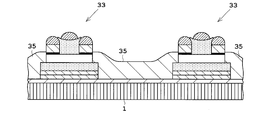
以上の製造方法よりTFT33が形成される。なお、図13に示すように、複数のTFT33の間は、例えばPIの絶縁膜35が形成される。絶縁膜35上に、ゲート電極31に信号を送信するためのゲート線(図示しない)や、データを読み出すためのデータ線(図示しない)が形成される。また、TFT33ごとにコンデンサ(図示しない)が形成される。なお、ゲート線、データ線およびコンデンサは、図14に示すゲート線104、データ線106およびコンデンサ101に対応する。
実施例に係る薄膜トランジスタ(TFT)33の製造方法によれば、凹凸パターンが形成されたスタンプ4の凹凸パターン面4aに、半導体層8、絶縁層9の順番で積層膜11を形成し、その積層膜11の最上層に、接続導電層10を形成する。一方、基板1上のほぼ全面に接続導電層3を形成する。そして、基板1にゲート電極31を形成する前に、凹凸パターン面4aの反対側の面4bからスタンプ4を加圧して、スタンプ4に形成された接続導電層10と、基板1に形成された接続導電層3とを接合させる。これにより、基板1に積層膜11が転写される。基板1上のほぼ全面に接続導電層3を形成しているので、スタンプ4を基板1上に載置した際に、スタンプ4に形成された接続導電層10と、基板1上に形成された接続導電層3とが接触した任意の位置で、接続導電層10と接続導電層3とが接合される。また、基板1にゲート電極31を形成する前に、基板1に半導体層8および絶縁膜9を含む積層膜11が転写される。したがって、スタンプ4による転写時における正確な位置合わせを不要とすることができる。
また、通常、転写は、大気中に浮遊する有機物が付着などすると接合しにくくなるので、真空中で行われる。しかしながら、本実施例では、接合面に接続導電層10と接続導電層3とを形成している。接続導電層10と接続導電層3をAu等の貴金属で構成すれば本質的に汚染が付着しにくくなる。もし汚染が付着しても接合前にUVオゾン照射法などでクリーニングすることで、大気圧中(真空チャンバ外)でも接合させることが可能となる。すなわち、高価な真空装置を使うことなく転写を容易に行うことができる。また、積層膜11は、導電層6と接続導電層10とで挟まれた構成になっているので、半導体膜8を汚染から防ぐことができる。
また、例えば、スタンプ4の凹凸パターン面4aと反対側の面(背面)4bから部材を押し当てて加圧する場合、その部材の表面形状等により、部材とスタンプ4との接触面内で加圧にばらつきが生じてしまう。スタンプ4の背面4bを気体で加圧することにより、例えば、スタンプ4のアレイ状に配置した凸部4cに形成された複数の積層膜11と基板1とを接触面内で均一に加圧することができる。
また、スタンプが高温になると熱膨張により変形するが、低温溶接(cold welding)で例えば常温で加圧することにより、スタンプの変形による寸法精度の悪化を抑えることができる。
バリアメタル層7は、半導体層8に直接、接続導電層6を形成する場合よりも、半導体層8と接続導電層6における密着性および導電率を良くすることができる。また、金属拡散防止や相互反応防止の効果も有する。積層膜11の最下層に接続導電層6を形成することにより、スタンプ4と積層膜11の離型性を良くすることができる。
従来のボトムゲートのTFTの構成では、グランド層は、ゲート線と同じ高さの層に形成される。グランド層が線として細く形成される場合、グランド層の抵抗が高くなり、それ自体が熱雑音の発生源となると共に、外来ノイズの影響も受けやすくなる。そのため、取得される画像にアーチファクトを生じさせていた。しかしながら、基板1上のほぼ全面にグランド層2を形成することで、抵抗を低くすることができ、ノイズを抑えることができる。これにより、アーチファクトを抑えることができる。また、従来、ゲート線およびデータ線と共に形成していたグランド線を形成しなくてもよいので、画素面積(画素ピッチ)を小さくすることができ、検出器等の解像度を上げることができる。グランド層2は、TFT33のバックゲートを外来ノイズ(電磁波)からシールドすることができる。グランド層2は、水蒸気や酸素を透過させないようにすることができる。
印刷法により積層膜11上にソース電極25およびドレイン電極27を容易に形成することができる。また、ソース電極25およびドレイン電極27をマスクとしてエッチングすることができるので、例えばレジスト膜を形成することをしなくてもよく、TFT33の製造を容易にすることができる。
半導体層8上にゲート絶縁膜29、ゲート電極31の順番でゲート絶縁膜29およびゲート電極31を印刷法により形成している。これにより、トップゲート型のTFT33を製造することができる。また、積層膜11を転写した後にゲート電極31を形成しているので、積層膜11が位置ズレして転写されても、位置ズレして転写された積層膜11に合わせてゲート電極31を形成することができる。すなわち、従来のボトムゲート型のTFTでは、ゲート電極に正確に位置合わせして、スタンプの半導体層と絶縁層を転写させていた。しかしながら、スタンプ4を柔らかい材料で構成しているので、一部で正確に位置合わせしても他部で位置ズレが生じていた。本実施例では、ゲート電極31が半導体層8と絶縁層9の転写後に形成されるので、スタンプ4の転写によるTFT33の歩留まりの低下を抑えることができる。
本発明は、上記実施形態に限られることはなく、下記のように変形実施することができる。
(1)上述した実施例において、スタンプ4の凸部4cは、1次元または2次元アレイ状に形成してもよい。これにより、薄膜トランジスタ(TFT)31は、1次元または2次元のアレイ状に形成される。
(2)上述した実施例において、スタンプ4のAuで構成される接続導電層10と、基板1のAuで構成される接続導電層3とを、低温溶接(cold welding)で接合させていた。すなわち、Au層とAu層で接合させていた。しかしながら、例えば、Ag層とAg層とで接合させてもよく、Au層とAg層またはAg層とAu層で接合させてもよい。
(3)上述した実施例において、バリアメタル層7、半導体層8および絶縁層9は、多層で構成されていてもよい。
Claims (9)
- 凹凸パターンが形成されたスタンプの凹凸パターン面に半導体層、絶縁層の順番で積層膜を形成する工程と、
前記スタンプに形成される前記積層膜の最上層に第1導電層を形成する工程と、
基板上の全面に第2導電層を形成する工程と、
前記基板にゲート電極を形成する前に、前記凹凸パターン面の反対側の面から前記スタンプを加圧して前記第1導電層と前記第2導電層とを接合させることにより、前記基板に前記スタンプの積層膜を転写する工程と、
を備えていることを特徴とする薄膜トランジスタの製造方法。 - 請求項1に記載された薄膜トランジスタの製造方法において、
前記転写する工程は、前記スタンプを気体で加圧することを特徴とする薄膜トランジスタの製造方法。 - 請求項1または2に記載された薄膜トランジスタの製造方法において、
前記転写する工程は、前記スタンプを常温で加圧することを特徴とする薄膜トランジスタの製造方法。 - 請求項1から3のいずれかに記載された薄膜トランジスタの製造方法において、
前記積層膜は、前記スタンプの凹凸パターン面にバリアメタル層、半導体層、絶縁層の順番で形成されていることを特徴とする薄膜トランジスタの製造方法。 - 請求項1から4のいずれかに記載された薄膜トランジスタの製造方法において、
前記スタンプに形成される前記積層膜の最下層に第3導電層を形成する工程を備えていることを特徴とする薄膜トランジスタの製造方法。 - 請求項1から5のいずれかに記載された薄膜トランジスタの製造方法において、
前記第2導電層を形成する前に、前記基板上の全面にグランド層を形成する工程を備えていることを特徴とする薄膜トランジスタの製造方法。 - 請求項1から6のいずれかに記載された薄膜トランジスタの製造方法において、
前記転写する工程の後に、前記積層膜上にソース電極およびドレイン電極を印刷法により形成する工程を備えていることを特徴とする薄膜トランジスタの製造方法。 - 請求項7に記載された薄膜トランジスタの製造方法において、
前記ソース電極および前記ドレイン電極をマスクとして前記第2導電層、前記第3導電層および前記バリアメタル層の少なくとも1つの層をエッチングする工程を備えていることを特徴とする薄膜トランジスタの製造方法。 - 請求項1から8のいずれかに記載された薄膜トランジスタの製造方法において、
前記転写する工程の後に、前記半導体層上にゲート絶縁膜、前記ゲート電極の順番で前記ゲート絶縁膜および前記ゲート電極を印刷法により形成する工程を備えていることを特徴とする薄膜トランジスタの製造方法。
Priority Applications (1)
| Application Number | Priority Date | Filing Date | Title |
|---|---|---|---|
| PCT/JP2011/005908 WO2013057771A1 (ja) | 2011-10-21 | 2011-10-21 | 薄膜トランジスタの製造方法 |
Applications Claiming Priority (1)
| Application Number | Priority Date | Filing Date | Title |
|---|---|---|---|
| PCT/JP2011/005908 WO2013057771A1 (ja) | 2011-10-21 | 2011-10-21 | 薄膜トランジスタの製造方法 |
Publications (1)
| Publication Number | Publication Date |
|---|---|
| WO2013057771A1 true WO2013057771A1 (ja) | 2013-04-25 |
Family
ID=48140451
Family Applications (1)
| Application Number | Title | Priority Date | Filing Date |
|---|---|---|---|
| PCT/JP2011/005908 Ceased WO2013057771A1 (ja) | 2011-10-21 | 2011-10-21 | 薄膜トランジスタの製造方法 |
Country Status (1)
| Country | Link |
|---|---|
| WO (1) | WO2013057771A1 (ja) |
Citations (6)
| Publication number | Priority date | Publication date | Assignee | Title |
|---|---|---|---|---|
| JP2009076729A (ja) * | 2007-09-21 | 2009-04-09 | Semiconductor Energy Lab Co Ltd | 半導体装置の作製方法 |
| JP2009088497A (ja) * | 2007-09-14 | 2009-04-23 | Semiconductor Energy Lab Co Ltd | 半導体装置及び電子機器 |
| JP2009533838A (ja) * | 2006-03-31 | 2009-09-17 | ソニー ドイチュラント ゲゼルシャフト ミット ベシュレンクテル ハフツング | 基板上への金属、金属酸化物および/または半導体材料のパターンの形成方法 |
| JP2010239123A (ja) * | 2009-03-12 | 2010-10-21 | Semiconductor Energy Lab Co Ltd | 半導体装置及びその作製方法 |
| JP2011009723A (ja) * | 2009-05-26 | 2011-01-13 | Semiconductor Energy Lab Co Ltd | Soi基板の作製方法 |
| WO2011058611A1 (ja) * | 2009-11-13 | 2011-05-19 | 株式会社島津製作所 | 薄膜トランジスタの製造方法 |
-
2011
- 2011-10-21 WO PCT/JP2011/005908 patent/WO2013057771A1/ja not_active Ceased
Patent Citations (6)
| Publication number | Priority date | Publication date | Assignee | Title |
|---|---|---|---|---|
| JP2009533838A (ja) * | 2006-03-31 | 2009-09-17 | ソニー ドイチュラント ゲゼルシャフト ミット ベシュレンクテル ハフツング | 基板上への金属、金属酸化物および/または半導体材料のパターンの形成方法 |
| JP2009088497A (ja) * | 2007-09-14 | 2009-04-23 | Semiconductor Energy Lab Co Ltd | 半導体装置及び電子機器 |
| JP2009076729A (ja) * | 2007-09-21 | 2009-04-09 | Semiconductor Energy Lab Co Ltd | 半導体装置の作製方法 |
| JP2010239123A (ja) * | 2009-03-12 | 2010-10-21 | Semiconductor Energy Lab Co Ltd | 半導体装置及びその作製方法 |
| JP2011009723A (ja) * | 2009-05-26 | 2011-01-13 | Semiconductor Energy Lab Co Ltd | Soi基板の作製方法 |
| WO2011058611A1 (ja) * | 2009-11-13 | 2011-05-19 | 株式会社島津製作所 | 薄膜トランジスタの製造方法 |
Similar Documents
| Publication | Publication Date | Title |
|---|---|---|
| TWI510145B (zh) | 電子裝置及其製造方法 | |
| US10723112B2 (en) | Method of transferring thin film | |
| JP2011142168A (ja) | 電子デバイスの製造方法および該電子デバイスに用いられる基板 | |
| TW201332768A (zh) | 電子裝置之製造方法 | |
| WO2011142089A1 (ja) | フレキシブル半導体装置およびその製造方法ならびに画像表示装置 | |
| TW201315593A (zh) | 電子裝置之製造方法、附樹脂層之載體基板之製造方法 | |
| TW201432971A (zh) | 電子裝置之製造方法及玻璃積層體之製造方法 | |
| CN102257617B (zh) | 光矩阵器件的制造方法 | |
| WO2009147769A1 (ja) | 表示装置の製造方法及び表示装置 | |
| JP5445590B2 (ja) | 薄膜トランジスタの製造方法 | |
| JP4205134B2 (ja) | 二次元画像検出器 | |
| JP2012138547A (ja) | フレキシブル電子デバイスの製造方法および樹脂層付積層基板、ならびにフレキシブル電子デバイス製造部材 | |
| JP5299190B2 (ja) | 光マトリックスデバイスの製造方法 | |
| WO2013057771A1 (ja) | 薄膜トランジスタの製造方法 | |
| JPWO2013057771A1 (ja) | 薄膜トランジスタの製造方法 | |
| JP2009130327A (ja) | 半導体装置の製造方法、電子機器の製造方法、半導体装置および電子機器 | |
| JP2014138179A (ja) | 薄膜トランジスタアレイ基板及び表示装置 | |
| JP5516196B2 (ja) | 薄膜トランジスタの製造方法 | |
| JP5960626B2 (ja) | 薄膜トランジスタを備えた半導体装置の製造方法 | |
| JP3670161B2 (ja) | 二次元画像検出器 | |
| JP4202315B2 (ja) | 二次元画像検出器 | |
| JP2014082386A (ja) | 有機トランジスタ及びその製造方法 | |
| JP2010267719A (ja) | 薄膜電子素子の製造方法 | |
| JP2010258348A (ja) | 光マトリックスデバイスの製造方法 | |
| JP2015023127A (ja) | 電子デバイスの製造方法 |
Legal Events
| Date | Code | Title | Description |
|---|---|---|---|
| 121 | Ep: the epo has been informed by wipo that ep was designated in this application |
Ref document number: 11874390 Country of ref document: EP Kind code of ref document: A1 |
|
| ENP | Entry into the national phase |
Ref document number: 2013539419 Country of ref document: JP Kind code of ref document: A |
|
| NENP | Non-entry into the national phase |
Ref country code: DE |
|
| 122 | Ep: pct application non-entry in european phase |
Ref document number: 11874390 Country of ref document: EP Kind code of ref document: A1 |